US5855268A - Optical sensor system for a bill validator - Google Patents
Optical sensor system for a bill validatorDownload PDFInfo
- Publication number
- US5855268A US5855268AUS08/941,400US94140097AUS5855268AUS 5855268 AUS5855268 AUS 5855268AUS 94140097 AUS94140097 AUS 94140097AUS 5855268 AUS5855268 AUS 5855268A
- Authority
- US
- United States
- Prior art keywords
- microcontroller
- variable gain
- gain amplifier
- optical sensor
- sensor system
- Prior art date
- Legal status (The legal status is an assumption and is not a legal conclusion. Google has not performed a legal analysis and makes no representation as to the accuracy of the status listed.)
- Expired - Lifetime
Links
Images


Classifications
- H—ELECTRICITY
- H03—ELECTRONIC CIRCUITRY
- H03G—CONTROL OF AMPLIFICATION
- H03G3/00—Gain control in amplifiers or frequency changers
- H03G3/20—Automatic control
- H03G3/30—Automatic control in amplifiers having semiconductor devices
- H03G3/3084—Automatic control in amplifiers having semiconductor devices in receivers or transmitters for electromagnetic waves other than radiowaves, e.g. lightwaves
- G—PHYSICS
- G07—CHECKING-DEVICES
- G07D—HANDLING OF COINS OR VALUABLE PAPERS, e.g. TESTING, SORTING BY DENOMINATIONS, COUNTING, DISPENSING, CHANGING OR DEPOSITING
- G07D7/00—Testing specially adapted to determine the identity or genuineness of valuable papers or for segregating those which are unacceptable, e.g. banknotes that are alien to a currency
- G07D7/06—Testing specially adapted to determine the identity or genuineness of valuable papers or for segregating those which are unacceptable, e.g. banknotes that are alien to a currency using wave or particle radiation
- G07D7/12—Visible light, infrared or ultraviolet radiation
- G07D7/121—Apparatus characterised by sensor details
- H—ELECTRICITY
- H03—ELECTRONIC CIRCUITRY
- H03G—CONTROL OF AMPLIFICATION
- H03G1/00—Details of arrangements for controlling amplification
- H03G1/0005—Circuits characterised by the type of controlling devices operated by a controlling current or voltage signal
- H03G1/0017—Circuits characterised by the type of controlling devices operated by a controlling current or voltage signal the device being at least one of the amplifying solid-state elements
- H03G1/0023—Circuits characterised by the type of controlling devices operated by a controlling current or voltage signal the device being at least one of the amplifying solid-state elements in emitter-coupled or cascode amplifiers
Definitions
- the present inventionpertains to a device and technique for providing a stable optical sensor system.
- the inventionconcerns a variable gain amplifier circuit for controlling leakage current in an optical sensor system of a bill validator, and a method for obtaining light measurements.
- Bill validators used in vending machines and the liketypically utilize optical, magnetic and other sensors to obtain measurements from an inserted bill to determine authenticity and denomination.
- the billis transported past a plurality of photosensors, typically made up of light-emitting diodes (LEDs) and phototransistors, and a plurality of signals are generated corresponding to measurements taken from different areas of the bill.
- the LED drive signalsare typically multiplexed between two or more LEDs to emit light at a number of wavelengths in a short period of time to ensure high security against fraud. The signals are then processed to validate and authenticate the bill.
- the output power of an LEDcan degrade on the order of fifty percent with aging, inserted bills are of differing quality, and bill path cleanliness may vary. Further, some bill validator applications require undiminished performance under harsh outdoor conditions such as extreme cold or heat, and such temperature changes can cause wildly varying gain characteristics in LED-receiver pairs resulting in erroneous sensor readings. In addition, there are normal production variations in LED optical power output and receiver sensitivity, which can lead to units having varying current and voltage requirements in order to operate effectively. In order to compensate for such phenomena, optical sensor measurements were taken over a large dynamic range.
- the inventionfeatures an improved optical sensor system for use in a currency validator.
- the optical sensor systemincludes a microcontroller, a plurality of light transmitters, a plurality of light receivers for producing signals, and a variable gain amplifier circuit connected to the receivers and to the microcontroller.
- the microcontrollercontrols the gain of the variable gain amplifier based on predetermined measurements of each light transmitter, and the variable gain amplifier includes dual transconductance amplifiers having an input signal applied to a bias current input and having their differential inputs inversely connected together to compensate for leakage current over a wide range of temperatures.
- the optical sensor systemmay also include one or more of the following features.
- a twelve-bit digital-to-analog convertermay be connected between the microcontroller and the plurality of light transmitters.
- a memory connected to the microcontrollermay be included for storing predetermined light transmitter and receiver circuit values.
- At least one of the light transmittersmay be an optical package containing at least two LEDs, wherein each LED transmits light of a different wavelength.
- a twelve-bit analog-to-digital convertermay be connected between the variable gain amplifier and the microcontroller, a gain digital-to-analog converter may be connected between the microcontroller and the variable gain amplifier, and a multiplexer may be connected between the receivers and the variable gain amplifier, and having an input connected to the microcontroller.
- a motor drive circuitmay be included for controlling a transport motor and a stacker motor.
- An operational transconductance amplifier circuithas dual transconductance amplifiers having an input signal applied to a bias current input, and having their differential inputs inversely connected together.
- variable gain amplifier circuitmay also include one or more of the following features.
- a transconductance amplifier circuitfor converting a voltage signal into a current signal output, wherein the output may be connected to the bias current input of the dual transconductance amplifiers.
- a variable transistormay be connected to the transconductance amplifier circuit for selecting the transconductance.
- An overcurrent protection circuitmay be connected between the transconductance amplifier and the operational transconductance amplifier circuit.
- a bill validatorincludes a variable gain amplifier with a continually adjustable gain driven by a twelve-bit gain DAC.
- a microprocessoruses a twelve-bit LED DAC for making LED current adjustments.
- the enhanced adjustability provided by this circuitryensures adequate signal levels for reliable LED and receiver pair operation over the validator's lifetime.
- such a designpermits using LED components with a wider distribution of characteristics, thus avoiding a costly sorting process during manufacturing to find LEDs that are within acceptable tolerance levels.
- the inventionalso provides low offsets across an extended temperature range through the use of leakage current compensation in the transconductance amplifiers of the variable gain amplifier circuitry. The result is consistent performance and security across the product's usable temperature range.
- the inventionprovides a stable, variable gain amplifier for use with an optical sensor system.
- the variable gain amplifieramplifies low level, medium bandwidth sensor signals at a continuously variable range of gains while maintaining low offsets over a wide temperature range.
- FIG. 1is a perspective view of a currency validator and transport unit
- FIG. 2Ais an enlarged side view of the interior of the bill validator and transport system of FIG. 1;
- FIG. 2Bis a simplified top view schematic diagram of the positions of some of LEDs in the bill validator and transport unit of FIG. 2A;
- FIG. 3is a simplified validator block diagram according to the invention.
- FIG. 4Ais a simplified circuit diagram of an embodiment of the LED circuitry of FIG. 3;
- FIG. 4Bis a circuit diagram of an embodiment of the receiver circuitry of FIG. 3.
- FIG. 5is a circuit diagram of variable gain amplifier circuitry according to the invention.
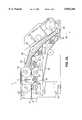
- FIG. 1is a perspective view of a currency validator and transport unit 1 connected to a bill stacker 2 and currency container or cashbox 4.
- currency used hereinmeans any paper currency, bill, banknote or other security document which may be used to pay for goods or services.
- the bill validator and transport unitmay have a bezel 6 designed to fit through an aperture in the front panel of a vending machine, gaming machine such as a slot machine, and the like.
- a bill entryway 8is incorporated in the bezel for the insertion of currency.
- FIG. 2Ais an enlarged side view of the interior of the bill validator and transport system 1.
- the bill entryway 8leads to a bill passageway 9.
- the beginning of the bill passagewayis defined by an upper housing 5 and a lower housing 7.
- Disposed on the bottom of the bill passagewayis a set of continuous belts 10 (one on each side of the bill passageway) which fit through openings (not shown) in the lower housing 7 to contact a bill.
- the belts 10are connected to a drive wheel 12, a pulley wheel 14 and various other tensioning wheels 16.
- a reversible transport motor 18is connected via a series of gears (not shown) to the drive wheels 12.
- Pulley wheels 20, 22are located on the top of the bill passageway which fit through openings in the upper housing 5 and are opposite the drive wheel and pulley wheel 14.
- a pair of continuous transport belts 24are connected to tensioning wheels 26 on the top of the bill passageway.
- the transport motor 18When a banknote is inserted into the currency validator and transport unit 1, one or more sensors cause the transport motor 18 to start.
- the billis gripped between the belts 10 and wheels 20 and advanced through the bill passageway 9 (from left to right in FIG. 2A) to encounter a plurality of optical and other sensors. If the information gathered by the sensors at any given point indicates that the bill is not genuine, then the transport motor 18 is reversed and the bill is rejected. Data collection continues until an escrow sensor (not shown) indicates that the bill transport should be stopped, at which time a braking signal is applied to the motor.
- the banknoteis then validated and denominated, and the vending machine checked to see if the proper merchandise is available.
- a currency validatorcontains a plurality of optical sensors located along the bill passageway 9 to generate electrical signals in response to features of a bill.
- FIG. 2Bis a simplified top view diagram 27 of the positions of the LEDs of the front optical sensors in the embodiment of FIG. 2A.
- These front optical sensorsare comprised of transmitters (for example, light emitting diodes or LEDs) and receivers (such as phototransistors) positioned in the upper housing 5 and lower housing 7 on opposite sides of the bill passageway 9 near the bill entryway 8.
- a bill 29would be inserted in the direction of arrow 28 to be transported between the front optical sensors.
- An optical escrow sensor(not shown) is also used to sense when the trailing edge of a bill has passed, and may be located in a position in the upper and lower housings in between the pulley wheels 20 and 22 (see FIG. 2A).
- the optical sensors used in the validator apparatusare encased in the upper and lower housings to prevent dirt and other foreign matter from adhering to the sensors, and to prevent tampering.
- at least one front optical sensortransmits and receives infra-red wavelength signals. Consequently, the upper and lower housings are preferably made of transparent plastic, in particular a red transparent plastic material having optical characteristics which permit the unobstructed transmission of infra-red waves.
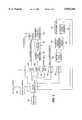
- FIG. 3is a simplified validator block diagram.
- a microcontroller 32is connected to an EEPROM 34, which stores predetermined values for use when processing signals from each of the optical transmitters (LEDs).
- the microcontrollerperforms all processing of signals to validate and denominate an inserted banknote, and transmits information such as credit data, hardware error messages, in-service and out-of-service messages and the like to the host system through host interface 36.
- the microcontrollercontrols each LED in the LED circuitry 38 through latch 37, and provides drive current through LED digital-to-analog converter (DAC) 40.
- DACdigital-to-analog converter
- a corresponding receiverWhen an LED is selected and energized, a corresponding receiver (one of the phototransistors in the receiver circuitry 42) generates a signal which is received by the microcontroller through multiplexer 44, variable gain amplifier 46, and a twelve-bit receiver analog-to-digital converter (ADC) 48.
- the microcontrolleralso controls the gain of the variable gain amplifier 46 through gain digital to analog converter (DAC) 50 for the particular receiver.
- DACdigital to analog converter
- the microcontrollerselects the receiver of interest by specifying an address through latch 52 to multiplexer 44.
- the microcontroller 32is also connected to the transport motor 18 and stacker motor 56 through a latch 53 and a motor drive circuit 54.
- the transport motorhas an associated tachometer 57 for accurately monitoring the position of a banknote in the banknote passageway 9, and the stacker motor has an associated stacker home sensor 58 for monitoring the home position of the bill stacker.
- the escrow sensor, tachometer 57 and stacker home sensor 58provide accurate information regarding bill position in the device.
- the LED DAC 40 and gain DAC 50are preset to appropriate settings during calibration of the bill validator optical sensors. Calibration occurs when the validator is placed in calibration mode and white paper having transmissivity and diffusion characteristics similar to a banknote is inserted.
- the validatorsets the gain DAC to an arbitrary number (for example, 1400 out of a full scale of 4095), and adjusts the LED DAC setting for each LED until the ADC 48 reading for that LED is equal to the arbitrary number (e.g. 1400).
- the setting value of the LED DAC for each LEDcan then be permanently stored in EEPROM 34, so that any time a given LED is turned ON its corresponding LED DAC setting is recalled and used. Alternately, the settings for the LED DAC and gain DAC can be calculated as the bill validator is used by the microcontroller.
- the microcontroller 32directs transport drive motor 18 to drive the banknote between the LED circuits 38 and receivers 42 to obtain measurements of the light transmitted through the banknote.
- measurements of the light transmission characteristics of the banknoteare utilized to authenticate the bill, and these bill validation measurements are taken until the bill clears the front optical sensors.
- FIG. 4Ais a simplified circuit diagram of an embodiment of the LED circuitry 38.
- the cross channel (CC) LED 60the start right (SR) LED 61, the start left (SL) LED 62, and recognition LED group one 64 and recognition LED group two 65.
- the recognition LED groupsmay contain two or more LEDs, wherein each LED in a recognition group may be of a different wavelength than the other LED(S) in that group.
- one LED in the recognition group 64 and one LED in recognition group 65may transmit light of Xnm wavelength, while another LED in each may transmit light of Ynm wavelength.
- a third wavelength light of Znmcould also be present.
- the microcontrollerselects which LEDs to turn ON in which recognition unit via the select lines A, B and C respectively labelled 67, 68 and 69.
- FIG. 4Bis a circuit diagram of the receiver circuitry 42 of FIG. 3 connected to a multiplexer 44. As shown, an escrow position phototransistor 80, a left start phototransistor 81, a right start phototransistor 82 and a cross-channel phototransistor are connected directly to the multiplexer 44. Also connected to the multiplexer through amplifier circuitry are recognition receivers A, B, C and D, or phototransistors 84, 85, 86 and 87, respectively. The microcontroller 32 selects the appropriate receiver or phototransistor by sending the select signals on select lines 67, 68 and 69. The output of the multiplexer 44 is then sent to the variable gain amplifier 46.
- FIG. 5is a circuit diagram of the variable gain amplifier 46 of FIG. 3.
- a transconductance amplifier 90is comprised of an operational amplifier 91, transistors 92 and 93 and resistors R1, R2 and R3.
- the transconductance amplifier 90has a gain proportional to the input signal on line 94, and takes the input voltage from one of the receiver phototransistors chosen in multiplexer 44 and converts it to a current flowing into the collector of transistor 92.
- the transconductance of this stageis selectable via transistor 93 and the values of R2 and R3 to either 303 uA/V or 13.6 uA/V.
- R1serves to limit the maximum current flowing through the transistor 92.
- the current in transistor 92is mirrored by transistors Q2-Q4 so that the current flowing out of the collector of Q4 is roughly equal to the current flowing into the collector of the transistor 92.
- the combination of Q6 and R4form an overcurrent protect circuit 95 for the bias current input (pin 1) of U2A.
- An operational transconductance amplifier circuit 100is formed of dual transconductance amplifiers U2A 96 and U2B 97, and functions as a variable gain block. The gain is controlled by a 0-4 volt signal applied at the gain control input line 98 at resistor R6.
- the operational transconductance amplifiercomprising amplifiers 96 and 97 (such as an LM13600 manufactured by National Semiconductor of California) has linearizing diodes that are used to convert the voltage across R6 into a linear bias for the differential inputs of U2A 96 and U2B 97.
- the input signalis fed (as a current) into the bias current input (pin 1) of U2A.
- This inputis conventionally used as a gain control input in operational transconductance amplifiers, with the amplified signal fed to the differential inputs.
- the input signal to the bias current inputmuch lower offsets are achieved, with the prime source of offsets being leakage currents in the current mirror at the bias current input rather than poor transistor matching in the input differential pair.
- the maximum bias current leakage specification for the LM13600is 100 nA at a temperature of 25° C., which would result in a 10 mV offset across resistor R9. This offset increases by about a decade for every 40° C., so if the transconductance amplifiers U2A and U2B (96 and 97) were connected in a conventional manner, at a temperature of 65° C. the offset could grow to an objectionable 100 mV. To compensate for these temperature induced offsets, the differential inputs of U2B 96 are inversely connected to the differential inputs of U2A 97 as shown in FIG. 6, such that the gain of U2B is -1 times the gain of U2A.
- the bias current input of U2Bis connected to a -5V source, so that the only current flowing into the output (pin 12) is due to leakage current.
- This output pinis tied to the output of U2A (pin 5) such that the leakage current contribution of the signal current flowing out of pin 5 is compensated by the leakage current signal flowing into pin 12. In this manner offsets are compensated across a very wide range of temperatures to provide a stable variable gain amplifier circuit.
- the voltage at the output 99 of the transconductance amplifier circuit 100is limited by diode D1 and buffered by operational amplifier U1B, which acts as a typical voltage follower.
Landscapes
- Health & Medical Sciences (AREA)
- General Health & Medical Sciences (AREA)
- Toxicology (AREA)
- Physics & Mathematics (AREA)
- General Physics & Mathematics (AREA)
- Electromagnetism (AREA)
- Inspection Of Paper Currency And Valuable Securities (AREA)
- Photometry And Measurement Of Optical Pulse Characteristics (AREA)
- Amplifiers (AREA)
Abstract
Description
Claims (12)
Priority Applications (8)
| Application Number | Priority Date | Filing Date | Title |
|---|---|---|---|
| US08/941,400US5855268A (en) | 1997-10-01 | 1997-10-01 | Optical sensor system for a bill validator |
| EP98951988AEP0954823B1 (en) | 1997-10-01 | 1998-09-30 | Variable gain amplifier and optical sensor system for a bill validator |
| AU97799/98AAU751013B2 (en) | 1997-10-01 | 1998-09-30 | Optical sensor system for a bill validator |
| DE69830230TDE69830230T2 (en) | 1997-10-01 | 1998-09-30 | AMPLIFIER WITH VARIABLE AMPLIFICATION AND OPTICAL SENSOR SYSTEM FOR MONITORING INSPECTION |
| CA002271746ACA2271746A1 (en) | 1997-10-01 | 1998-09-30 | Optical sensor system for a bill validator |
| BR9806260-3ABR9806260A (en) | 1997-10-01 | 1998-09-30 | Optical sensor system for banknote validator. |
| ES98951988TES2241171T3 (en) | 1997-10-01 | 1998-09-30 | VARIABLE GAIN AMPLIFIER AND OPTICAL SENSOR SYSTEM FOR A MONEY CHECK. |
| PCT/US1998/020418WO1999017248A1 (en) | 1997-10-01 | 1998-09-30 | Optical sensor system for a bill validator |
Applications Claiming Priority (1)
| Application Number | Priority Date | Filing Date | Title |
|---|---|---|---|
| US08/941,400US5855268A (en) | 1997-10-01 | 1997-10-01 | Optical sensor system for a bill validator |
Publications (1)
| Publication Number | Publication Date |
|---|---|
| US5855268Atrue US5855268A (en) | 1999-01-05 |
Family
ID=25476404
Family Applications (1)
| Application Number | Title | Priority Date | Filing Date |
|---|---|---|---|
| US08/941,400Expired - LifetimeUS5855268A (en) | 1997-10-01 | 1997-10-01 | Optical sensor system for a bill validator |
Country Status (8)
| Country | Link |
|---|---|
| US (1) | US5855268A (en) |
| EP (1) | EP0954823B1 (en) |
| AU (1) | AU751013B2 (en) |
| BR (1) | BR9806260A (en) |
| CA (1) | CA2271746A1 (en) |
| DE (1) | DE69830230T2 (en) |
| ES (1) | ES2241171T3 (en) |
| WO (1) | WO1999017248A1 (en) |
Cited By (20)
| Publication number | Priority date | Publication date | Assignee | Title |
|---|---|---|---|---|
| US5999052A (en)* | 1998-04-28 | 1999-12-07 | Lucent Technologies Inc. | High speed, fine-resolution gain programmable amplifier |
| US6193392B1 (en) | 1999-05-27 | 2001-02-27 | Pervaiz Lodhie | Led array with a multi-directional, multi-functional light reflector |
| US6292579B1 (en)* | 1998-02-09 | 2001-09-18 | Mars Incorporated | Document validator having an inductive sensor |
| US6473165B1 (en) | 2000-01-21 | 2002-10-29 | Flex Products, Inc. | Automated verification systems and methods for use with optical interference devices |
| US6677818B2 (en)* | 2000-08-03 | 2004-01-13 | Broadcom Corporation | Method and circuit for a dual supply amplifier |
| US20040199468A1 (en)* | 2003-03-14 | 2004-10-07 | Muneharu Nakabayashi | Sheet handling apparatus |
| US20040217536A1 (en)* | 2001-09-28 | 2004-11-04 | Atsushi Isobe | Paper sheet handling apparatus |
| US6970236B1 (en) | 2002-08-19 | 2005-11-29 | Jds Uniphase Corporation | Methods and systems for verification of interference devices |
| US7289149B1 (en) | 2002-03-29 | 2007-10-30 | Sensata Technologies, Inc. | Operational transconductance amplifier for high-speed, low-power imaging applications |
| USD580580S1 (en) | 2008-01-11 | 2008-11-11 | Pervaiz Lodhie | Circular light structure |
| US20090109676A1 (en)* | 2007-10-30 | 2009-04-30 | Pervaiz Lodhie | Loop led light |
| US20090109674A1 (en)* | 2007-10-25 | 2009-04-30 | Pervaiz Lodhie | Led light |
| USD613886S1 (en) | 2008-06-10 | 2010-04-13 | Pervaiz Lodhie | LED light module with cutouts |
| USD613885S1 (en) | 2008-06-10 | 2010-04-13 | Pervaiz Lodhie | Two-stage LED light module |
| USD614318S1 (en) | 2008-06-10 | 2010-04-20 | Pervaiz Lodhie | LED light module |
| US20100259749A1 (en)* | 2006-08-22 | 2010-10-14 | Mei, Inc | Optical detector arrangement for document acceptor |
| USD631567S1 (en) | 2008-01-11 | 2011-01-25 | Pervaiz Lodhie | LED bulb |
| US20110264261A1 (en)* | 2008-01-29 | 2011-10-27 | Intelligent Currency Solutions | System and Method for Independent Verification of Circulating Bank Notes |
| US20130328689A1 (en)* | 2012-06-11 | 2013-12-12 | Oki Electric Industry Co., Ltd. | Medium processor notifying when servicing is required |
| US10325436B2 (en) | 2015-12-31 | 2019-06-18 | Hand Held Products, Inc. | Devices, systems, and methods for optical validation |
Families Citing this family (1)
| Publication number | Priority date | Publication date | Assignee | Title |
|---|---|---|---|---|
| US6671676B1 (en) | 2000-05-04 | 2003-12-30 | Metreo Markets, Inc. | Method and apparatus for analyzing and allocating resources of time-varying value using recursive lookahead |
Citations (12)
| Publication number | Priority date | Publication date | Assignee | Title |
|---|---|---|---|---|
| EP0078708A2 (en)* | 1981-11-03 | 1983-05-11 | De La Rue Systems Limited | Apparatus for sorting sheets according to their patterns |
| US4406996A (en)* | 1980-06-27 | 1983-09-27 | Laurel Bank Machine Co., Ltd. | Intensity compensator circuit for optical sensor in bank note machine |
| US4628194A (en)* | 1984-10-10 | 1986-12-09 | Mars, Inc. | Method and apparatus for currency validation |
| US4651292A (en)* | 1982-04-05 | 1987-03-17 | Robert Bosch Gmbh | Temperature compensation of a linear sensor |
| US4769532A (en)* | 1986-07-11 | 1988-09-06 | Laurel Bank Machines Co., Ltd. | Apparatus for adjusting optical sensors with threshold memory |
| GB2219855A (en)* | 1988-05-31 | 1989-12-20 | Laurel Bank Machine Co | Bill discriminating apparatus |
| US4947441A (en)* | 1988-05-20 | 1990-08-07 | Laurel Bank Machine Co., Ltd. | Bill discriminating apparatus |
| US5027415A (en)* | 1988-05-31 | 1991-06-25 | Laurel Bank Machines Co., Ltd. | Bill discriminating apparatus |
| US5167313A (en)* | 1990-10-10 | 1992-12-01 | Mars Incorporated | Method and apparatus for improved coin, bill and other currency acceptance and slug or counterfeit rejection |
| US5465821A (en)* | 1993-02-18 | 1995-11-14 | Laurel Bank Machine Co., Ltd. | Sheet discriminating apparatus |
| US5682119A (en)* | 1995-03-01 | 1997-10-28 | Nec Corporation | Variable gain circuit |
| US5709293A (en)* | 1994-03-10 | 1998-01-20 | Kabushiki Kaisha Nippon Conlux | Bill processing device |
- 1997
- 1997-10-01USUS08/941,400patent/US5855268A/ennot_activeExpired - Lifetime
- 1998
- 1998-09-30EPEP98951988Apatent/EP0954823B1/ennot_activeExpired - Lifetime
- 1998-09-30ESES98951988Tpatent/ES2241171T3/ennot_activeExpired - Lifetime
- 1998-09-30WOPCT/US1998/020418patent/WO1999017248A1/enactiveIP Right Grant
- 1998-09-30BRBR9806260-3Apatent/BR9806260A/ennot_activeIP Right Cessation
- 1998-09-30DEDE69830230Tpatent/DE69830230T2/ennot_activeExpired - Lifetime
- 1998-09-30AUAU97799/98Apatent/AU751013B2/ennot_activeCeased
- 1998-09-30CACA002271746Apatent/CA2271746A1/ennot_activeAbandoned
Patent Citations (15)
| Publication number | Priority date | Publication date | Assignee | Title |
|---|---|---|---|---|
| US4406996A (en)* | 1980-06-27 | 1983-09-27 | Laurel Bank Machine Co., Ltd. | Intensity compensator circuit for optical sensor in bank note machine |
| EP0078708A2 (en)* | 1981-11-03 | 1983-05-11 | De La Rue Systems Limited | Apparatus for sorting sheets according to their patterns |
| US4651292A (en)* | 1982-04-05 | 1987-03-17 | Robert Bosch Gmbh | Temperature compensation of a linear sensor |
| US4628194A (en)* | 1984-10-10 | 1986-12-09 | Mars, Inc. | Method and apparatus for currency validation |
| US4769532A (en)* | 1986-07-11 | 1988-09-06 | Laurel Bank Machines Co., Ltd. | Apparatus for adjusting optical sensors with threshold memory |
| US4947441A (en)* | 1988-05-20 | 1990-08-07 | Laurel Bank Machine Co., Ltd. | Bill discriminating apparatus |
| GB2219855A (en)* | 1988-05-31 | 1989-12-20 | Laurel Bank Machine Co | Bill discriminating apparatus |
| US5027415A (en)* | 1988-05-31 | 1991-06-25 | Laurel Bank Machines Co., Ltd. | Bill discriminating apparatus |
| US5167313A (en)* | 1990-10-10 | 1992-12-01 | Mars Incorporated | Method and apparatus for improved coin, bill and other currency acceptance and slug or counterfeit rejection |
| US5330041A (en)* | 1990-10-10 | 1994-07-19 | Mars Incorporated | Method and apparatus for improved coin, bill and other currency acceptance and slug or counterfeit rejection |
| US5443144A (en)* | 1990-10-10 | 1995-08-22 | Mars Incorporated | Method and apparatus for improved coin, bill and other currency acceptance and slug or counterfeit rejection |
| US5564548A (en)* | 1990-10-10 | 1996-10-15 | Mars Incorporated | Method and apparatus for currency acceptance and slug or counterfeit rejection |
| US5465821A (en)* | 1993-02-18 | 1995-11-14 | Laurel Bank Machine Co., Ltd. | Sheet discriminating apparatus |
| US5709293A (en)* | 1994-03-10 | 1998-01-20 | Kabushiki Kaisha Nippon Conlux | Bill processing device |
| US5682119A (en)* | 1995-03-01 | 1997-10-28 | Nec Corporation | Variable gain circuit |
Cited By (44)
| Publication number | Priority date | Publication date | Assignee | Title |
|---|---|---|---|---|
| US6292579B1 (en)* | 1998-02-09 | 2001-09-18 | Mars Incorporated | Document validator having an inductive sensor |
| US5999052A (en)* | 1998-04-28 | 1999-12-07 | Lucent Technologies Inc. | High speed, fine-resolution gain programmable amplifier |
| US6193392B1 (en) | 1999-05-27 | 2001-02-27 | Pervaiz Lodhie | Led array with a multi-directional, multi-functional light reflector |
| US20050217969A1 (en)* | 2000-01-21 | 2005-10-06 | Jds Uniphase Corporation | Automated verification systems and method for use with optical interference devices |
| US6473165B1 (en) | 2000-01-21 | 2002-10-29 | Flex Products, Inc. | Automated verification systems and methods for use with optical interference devices |
| US7184133B2 (en) | 2000-01-21 | 2007-02-27 | Jds Uniphase Corporation | Automated verification systems and method for use with optical interference devices |
| US7006204B2 (en) | 2000-01-21 | 2006-02-28 | Flex Products, Inc. | Automated verification systems and methods for use with optical interference devices |
| US6677818B2 (en)* | 2000-08-03 | 2004-01-13 | Broadcom Corporation | Method and circuit for a dual supply amplifier |
| US6828854B2 (en) | 2000-08-03 | 2004-12-07 | Broadcom Corporation | Method and circuit for a dual supply amplifier |
| US20050083126A1 (en)* | 2000-08-03 | 2005-04-21 | Broadcom Corporation | Method and circuit for a dual supply amplifier |
| US7012464B2 (en) | 2000-08-03 | 2006-03-14 | Broadcom Corporation | Method and circuit for a dual supply amplifier |
| US20040135638A1 (en)* | 2000-08-03 | 2004-07-15 | Broadcom Corporation | Method and circuit for a dual supply amplifier |
| US20040217536A1 (en)* | 2001-09-28 | 2004-11-04 | Atsushi Isobe | Paper sheet handling apparatus |
| US7841459B2 (en)* | 2001-09-28 | 2010-11-30 | Japan Cash Machine Co., Ltd. | Paper sheet handling apparatus |
| US7289149B1 (en) | 2002-03-29 | 2007-10-30 | Sensata Technologies, Inc. | Operational transconductance amplifier for high-speed, low-power imaging applications |
| US6970236B1 (en) | 2002-08-19 | 2005-11-29 | Jds Uniphase Corporation | Methods and systems for verification of interference devices |
| US20040199468A1 (en)* | 2003-03-14 | 2004-10-07 | Muneharu Nakabayashi | Sheet handling apparatus |
| US8836926B2 (en) | 2006-08-22 | 2014-09-16 | Mei, Inc. | Optical detector arrangement for document acceptor |
| US20100259749A1 (en)* | 2006-08-22 | 2010-10-14 | Mei, Inc | Optical detector arrangement for document acceptor |
| US20110122622A1 (en)* | 2007-10-25 | 2011-05-26 | Pervaiz Lodhie | LED Light |
| US7862204B2 (en) | 2007-10-25 | 2011-01-04 | Pervaiz Lodhie | LED light |
| US8157416B2 (en) | 2007-10-25 | 2012-04-17 | Pervaiz Lodhie | LED light |
| US8128258B2 (en) | 2007-10-25 | 2012-03-06 | Pervaiz Lodhie | LED light |
| US20110128736A1 (en)* | 2007-10-25 | 2011-06-02 | Pervaiz Lodhie | LED Light |
| US20090109674A1 (en)* | 2007-10-25 | 2009-04-30 | Pervaiz Lodhie | Led light |
| US7784967B2 (en) | 2007-10-30 | 2010-08-31 | Pervaiz Lodhie | Loop LED light |
| US20090109676A1 (en)* | 2007-10-30 | 2009-04-30 | Pervaiz Lodhie | Loop led light |
| US20110002121A1 (en)* | 2007-10-30 | 2011-01-06 | Pervaiz Lodhie | Loop LED Light |
| USD631567S1 (en) | 2008-01-11 | 2011-01-25 | Pervaiz Lodhie | LED bulb |
| USD599496S1 (en) | 2008-01-11 | 2009-09-01 | Pervaiz Lodhie | Circular light structure |
| USD580580S1 (en) | 2008-01-11 | 2008-11-11 | Pervaiz Lodhie | Circular light structure |
| USD595886S1 (en) | 2008-01-11 | 2009-07-07 | Pervaiz Lodhie | Circular light structure |
| US20110264261A1 (en)* | 2008-01-29 | 2011-10-27 | Intelligent Currency Solutions | System and Method for Independent Verification of Circulating Bank Notes |
| US8322604B2 (en)* | 2008-01-29 | 2012-12-04 | Intelligent Currency Solutions | System and method for independent verification of circulating bank notes |
| USD631601S1 (en) | 2008-06-10 | 2011-01-25 | Pervaiz Lodhie | LED light module with cutouts |
| USD614318S1 (en) | 2008-06-10 | 2010-04-20 | Pervaiz Lodhie | LED light module |
| USD630372S1 (en) | 2008-06-10 | 2011-01-04 | Pervaiz Lodhie | Two-stage LED light module |
| USD613885S1 (en) | 2008-06-10 | 2010-04-13 | Pervaiz Lodhie | Two-stage LED light module |
| USD613886S1 (en) | 2008-06-10 | 2010-04-13 | Pervaiz Lodhie | LED light module with cutouts |
| USD629957S1 (en) | 2008-06-10 | 2010-12-28 | Pervaiz Lodhie | LED light module |
| US20130328689A1 (en)* | 2012-06-11 | 2013-12-12 | Oki Electric Industry Co., Ltd. | Medium processor notifying when servicing is required |
| US10325436B2 (en) | 2015-12-31 | 2019-06-18 | Hand Held Products, Inc. | Devices, systems, and methods for optical validation |
| US11282323B2 (en) | 2015-12-31 | 2022-03-22 | Hand Held Products, Inc. | Devices, systems, and methods for optical validation |
| US11854333B2 (en) | 2015-12-31 | 2023-12-26 | Hand Held Products, Inc. | Devices, systems, and methods for optical validation |
Also Published As
| Publication number | Publication date |
|---|---|
| BR9806260A (en) | 2000-01-25 |
| ES2241171T3 (en) | 2005-10-16 |
| EP0954823A4 (en) | 2000-11-15 |
| EP0954823B1 (en) | 2005-05-18 |
| DE69830230T2 (en) | 2006-02-02 |
| WO1999017248A8 (en) | 1999-06-10 |
| DE69830230D1 (en) | 2005-06-23 |
| AU751013B2 (en) | 2002-08-08 |
| EP0954823A1 (en) | 1999-11-10 |
| CA2271746A1 (en) | 1999-04-08 |
| AU9779998A (en) | 1999-04-23 |
| WO1999017248A1 (en) | 1999-04-08 |
Similar Documents
| Publication | Publication Date | Title |
|---|---|---|
| US5855268A (en) | Optical sensor system for a bill validator | |
| US5027415A (en) | Bill discriminating apparatus | |
| US6223876B1 (en) | Bank note validator | |
| US5476169A (en) | Bill discriminating apparatus for bill handling machine | |
| US5301786A (en) | Method and apparatus for validating a paper-like piece | |
| US4875589A (en) | Monitoring system | |
| US6677603B2 (en) | Paper sheet discriminating device | |
| EP2099704A1 (en) | Method of monitoring a sequence of documents | |
| KR101046247B1 (en) | Banknote Detection Unit for Banknote Discrimination Device | |
| GB2444966A (en) | Validating sheet objects with a barcode and money value | |
| MXPA99004978A (en) | Optical sensor system for a bill validator | |
| JP3642577B2 (en) | Bill discrimination device | |
| US7049572B2 (en) | Optical sensor and method of operation thereof | |
| JP3720995B2 (en) | Medium number detection method and apparatus | |
| JPH0814859B2 (en) | Paper discrimination device | |
| US7910903B2 (en) | Optical sensor with a counter for counting items and controlling a light source | |
| KR101072766B1 (en) | Method for correcting the result of paper money thickness measurement | |
| JP3332956B2 (en) | Banknote recognition device | |
| JPH1173532A (en) | Paper form identification device | |
| EP1675071A1 (en) | Sensor temperature control | |
| JP2001126108A (en) | Banknote recognition device | |
| MXPA98010172A (en) | Validator of bancar documents |
Legal Events
| Date | Code | Title | Description |
|---|---|---|---|
| AS | Assignment | Owner name:MARS INCORPORATED, VIRGINIA Free format text:ASSIGNMENT OF ASSIGNORS INTEREST;ASSIGNOR:ZOLADZ, EDWARD M. JR.;REEL/FRAME:008893/0267 Effective date:19971229 | |
| STCF | Information on status: patent grant | Free format text:PATENTED CASE | |
| CC | Certificate of correction | ||
| FPAY | Fee payment | Year of fee payment:4 | |
| FPAY | Fee payment | Year of fee payment:8 | |
| AS | Assignment | Owner name:CITIBANK, N.A., TOKYO BRANCH,JAPAN Free format text:SECURITY AGREEMENT;ASSIGNOR:MEI, INC.;REEL/FRAME:017811/0716 Effective date:20060619 Owner name:CITIBANK, N.A., TOKYO BRANCH, JAPAN Free format text:SECURITY AGREEMENT;ASSIGNOR:MEI, INC.;REEL/FRAME:017811/0716 Effective date:20060619 | |
| AS | Assignment | Owner name:MEI, INC.,PENNSYLVANIA Free format text:ASSIGNMENT OF ASSIGNORS INTEREST;ASSIGNOR:MARS, INCORPORATED;REEL/FRAME:017882/0715 Effective date:20060619 Owner name:MEI, INC., PENNSYLVANIA Free format text:ASSIGNMENT OF ASSIGNORS INTEREST;ASSIGNOR:MARS, INCORPORATED;REEL/FRAME:017882/0715 Effective date:20060619 | |
| AS | Assignment | Owner name:CITIBANK JAPAN LTD., JAPAN Free format text:CHANGE OF SECURITY AGENT;ASSIGNOR:CITIBANK, N.A.., TOKYO BRANCH;REEL/FRAME:019699/0342 Effective date:20070701 Owner name:CITIBANK JAPAN LTD.,JAPAN Free format text:CHANGE OF SECURITY AGENT;ASSIGNOR:CITIBANK, N.A.., TOKYO BRANCH;REEL/FRAME:019699/0342 Effective date:20070701 | |
| FPAY | Fee payment | Year of fee payment:12 | |
| AS | Assignment | Owner name:MEI, INC., PENNSYLVANIA Free format text:RELEASE BY SECURED PARTY;ASSIGNOR:CITIBANK JAPAN LTD.;REEL/FRAME:031074/0602 Effective date:20130823 | |
| AS | Assignment | Owner name:GOLDMAN SACHS BANK USA, AS COLLATERAL AGENT, NEW Y Free format text:SECURITY AGREEMENT;ASSIGNOR:MEI, INC.;REEL/FRAME:031095/0513 Effective date:20130822 | |
| AS | Assignment | Owner name:MEI, INC., PENNSYLVANIA Free format text:RELEASE OF SECURITY INTEREST IN INTELLECTUAL PROPERTY COLLATERAL RECORDED AT REEL/FRAME 031095/0513;ASSIGNOR:GOLDMAN SACHS BANK USA, AS COLLATERAL AGENT;REEL/FRAME:031796/0123 Effective date:20131211 | |
| AS | Assignment | Owner name:CRANE PAYMENT INNOVATIONS, INC., PENNSYLVANIA Free format text:CHANGE OF NAME;ASSIGNOR:MEI, INC.;REEL/FRAME:036981/0237 Effective date:20150122 |