US5854918A - Apparatus and method for self-timed algorithmic execution - Google Patents
Apparatus and method for self-timed algorithmic executionDownload PDFInfo
- Publication number
- US5854918A US5854918AUS08/590,499US59049996AUS5854918AUS 5854918 AUS5854918 AUS 5854918AUS 59049996 AUS59049996 AUS 59049996AUS 5854918 AUS5854918 AUS 5854918A
- Authority
- US
- United States
- Prior art keywords
- pulse
- logic
- self
- timed
- rate
- Prior art date
- Legal status (The legal status is an assumption and is not a legal conclusion. Google has not performed a legal analysis and makes no representation as to the accuracy of the status listed.)
- Expired - Lifetime
Links
Images


Classifications
- G—PHYSICS
- G06—COMPUTING OR CALCULATING; COUNTING
- G06F—ELECTRIC DIGITAL DATA PROCESSING
- G06F7/00—Methods or arrangements for processing data by operating upon the order or content of the data handled
Definitions
- the present inventionrelates generally to apparatus and methods for generating internal timing signals for high-speed computer systems. More particularly, the present invention is an apparatus and method for self-timed algorithmic execution, which is not rigidly synchronized to a master time base.
- one unitary clock signalis rebuffered through several clock amplifiers to act as the lone source of timing synchronization for all of the memory devices employed in the system.
- several additional differently phased clock signalsmay be used to drive separate sets of memory devices, yet all are conventionally synchronized to the master time base in the system.
- the different memory devicestoggle or change state with data streams or instruction sequences at relatively different rates.
- Such multiply clocked circuitsare often designed such that functional logic between the memory devices may cycle, at it's fastest possible rate.
- the functional logicis apportioned among the memory devices so that a system-design constraint of a target minimum execution time is maintained without a co-constraining increase in the number of functional logic or memory device elements.
- a superharmonic clockis used to pace the internal ranks of certain pipelined functional units at a faster rate while the input-output boundaries of the functional unit are paced at a slower rate compatible with the rest of the pipelined functional units in the system.
- This prior art methodis known as "micropipelining" and involves apparatus in which the inner memory devices of a pipelined functional unit have a strictly synchronous superharmonic clock signal that interleaves the microoperations of the pipeline synchronism with the slower stream rate experienced at the input-ports and output-ports of the pipeline.
- micropipelining's drawbacksinclude requiring several clock amplifiers in a low-skew tree organization, to ensure a lowest possible skew in the triggering signal actually received by each of the memory devices, and requiring a unitized timing interval.
- sets of logic elements within a micropipeline that do not have propagation delays short enough to operate within the unitized timing intervalare difficult to accommodate.
- micropipelining conceptsare particularly difficult to implement using reconfigurable logic devices (RLDs), such as Field Programmable Gate Arrays (FPGAs), since the propagation delays within an RLD vary from functional unit to functional unit making it difficult to have a semi-global micropipeline clock.
- RLDsreconfigurable logic devices
- FPGAsField Programmable Gate Arrays
- RLDRegister Transfer Language
- Such a paradigmrelies heavily on the existence of separate master time base clocks for driving the functional logic and memory devices within the RLD.
- Such a paradigmalso ignores the effects that the physical implementation of the logic design within the RLD will have on the logic design's overall timing performance and silicon resource requirements.
- RLD tool manufacturersoften claim that an "advantage" of their logic design paradigm is that it is not tailored to the RLD's physical characteristics.
- the present inventionis an apparatus and method for self-timed algorithmic execution.
- the apparatus of the present inventionpreferably comprises a functional logic set, a reference clock input and a pulse sequencer.
- the functional logic setreceives input data in synchrony with a reference clock received at the reference clock input; performs algorithmic computations on the input data at a maximal-rate determined by the pulse sequencer in accordance with the physical characteristics of the functional logic set; generates output data; and transmits the output data in synchrony with the reference clock.
- the maximal-rate set by the pulse sequenceris independent of the reference clock.
- the method of the present inventionpreferably comprises the steps of: transferring input data to a functional logic set in synchrony with a reference clock; generating a maximal-rate pulse sequence, for driving the functional logic set at a rate dependent upon an algorithm execution time for the functional logic set but independent of the reference clock; generating output data from the functional logic set in response to the maximal-rate pulse sequence; and transferring the output data from the functional logic in synchrony with the reference clock.
- FIG. 1is a block diagram of a preferred embodiment of an apparatus for self-timed algorithmic execution
- FIG. 2Ais a block diagram of a preferred embodiment of a pulse sequencer of the present invention.
- FIG. 2Bis a block diagram of a preferred embodiment of start logic within the pulse sequencer
- FIG. 2Cis a block diagram of a preferred embodiment of a delay unit within the pulse sequencer
- FIG. 2Dis a block diagram of a preferred embodiment of a pulse counter within the pulse sequencer
- FIG. 2Eis a block diagram of a preferred embodiment of sequence gate logic within the pulse sequencer
- FIG. 3is a block diagram of a preferred embodiment of functional logic of the present invention.
- FIG. 4is a block diagram of a preferred embodiment of a multiplexor within the functional logic
- FIG. 5is a block diagram of a preferred embodiment of a partial product generator within the functional logic
- FIG. 6is a block diagram of a preferred embodiment of a partial product summer within the functional logic
- FIG. 7is a block diagram of a preferred embodiment of a product accumulator within the functional logic
- FIG. 8is a preferred timing diagram showing the operation of the present invention.
- FIG. 9Ais a matrix showing preferred partial product additions for a 16-bit by 16-bit multiplication of the present invention.
- FIG. 9Bis a matrix showing preferred partial product additions for an 8-bit by 8-bit multiplication of the present invention.
- FIG. 10is a flowchart of a preferred method for self-timed algorithmic execution
- FIG. 11is a flowchart of a preferred method for generating a pulse sequence.
- FIG. 12is a flowchart of a preferred method for generating output data in response to the pulse sequence.
- the present inventionis an apparatus and method for self-timed algorithmic execution.
- the present inventionexecutes the selected algorithm at its fastest possible speed independent of any reference clocks which drive other functional logic sets.
- timing characteristics of any functional logic set which implements the algorithmneed not be either constrained by or dependent upon a reference clock's speed.
- the present invention: first, accepts data from other functional logic sets; second, operates upon the data at a self-timed rate based upon a functional logic set which implements the algorithm in response to the generation of a set of self-timed pulses; and third, outputs data by a specific known time to be accepted by the other functional logic sets.
- the apparatus and method of the present inventionis particularly advantageous over the prior art because it enables one functional logic set to operate at a speed independent of the operational speed of other functional logic sets or reference clocks, thus simplifying hardware design while maintaining the fastest possible algorithmic execution speeds.
- the present inventionachieves these advantages by viewing functional logic sets in terms of their most fundamental physical structures.
- the present inventiondoes not rely upon a Register Transfer Logic (RTL) paradigm. Rather, the present invention tailors a unique timing circuit to a functional logic set which implements an algorithm so that the functional logic set may operate at its fastest possible rate.
- RTLRegister Transfer Logic
- the present inventiondefines a new paradigm for implementing logic designs within silicon resources by viewing the silicon resources as incremental arbiters not only of algorithmic execution but also of timing rates.
- the present inventionis preferably embodied in a Reconfigurable Logic Device (RLD), such as a Xilinx XC4000 series (Xilinx, San Jose, Calif.) Field Programmable Gate Array (FPGA).
- RLDsare comprised of a set of Configurable Logic Blocks (CLBs).
- CLBsConfigurable Logic Blocks
- Each CLBpreferably includes at least one function generator, as well as one or more carry logic elements.
- the FPGA's internal structureis dynamically reconfigurable through the use of a configuration data set, or configuration bit-stream.
- particular logic functionsare generated via the function generators, in accordance with the configuration bit-stream.
- Each function generatorhas a characteristic, stable signal propagation delay.
- a first and second function generator(types “F” and “G”) each have a propagation delay of approximately 4.5 nanoseconds (ns); and a third function generator (type “H”) has a propagation delay of approximately 2.5 ns.
- the carry logic elementstypically comprise carry-propagate logic designed to have very small, stable propagation delays.
- the carry-propagate logic within a Xilinx XC4000 series FPGAhas a propagation delay of 1.5 ns.
- the present inventioncreates multiple levels of feedback by selectively combining resources within the RLD to produce various internal propagation delays.
- This feedbackis used to create individual timing circuits for driving one or more functional logic sets within the RLD.
- the present inventionutilizes "inertial" delays rather than solely relying upon "pure” delays.
- An inertial delayis defined as a delay for which propagation requires a minimum pulse width, while a pure delay is one for which delay propagation is essentially pulse width independent.
- inertial delaysare stable, well-controlled delays.
- FIGS. 3 through 7 belowshow the details of an exemplary 16-bit by 16-bit multiplication yielding a 32-bit product.
- the present inventionmay be used to implement multiplications of greater or less than 16-bits.
- the signals and bits described belowpreferably have only two states, logic "1" and logic "0.” While the elements of the present invention will be described as responding only to rising edge of a state transition (i.e. a logic "0" to logic "1" transition), those skilled in the art will recognize that the RLD may be configured to respond to either only falling edge or both rising and falling edge state transitions.
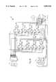
- the apparatus 20comprises an input buffer 22, functional logic 24, an output buffer 26, a synchronous state machine 30, and a pulse sequencer 34.
- the input buffer 22is a conventionally known device that loads either an X-bit multiplicand or a Y-bit multiplier received over line 19 from external circuitry (not shown) each time the external circuitry holds an input enable signal on line 29 in a logic "1" state while receiving a reference clock signal on line 28.
- the reference clockis preferably implemented using a clocking mechanism described in U.S. patent application Ser. No. 08/501,970, entitled System and Method for Phase-Synchronous, Flexible-Frequency Clocking and Messaging. Those skilled in the art will recognize that any conventionally known clock generation means may instead provide the reference clock.
- the input buffer 22outputs the X-bit multiplicand over line 21 and the Y-bit multiplier over line 23 to the functional logic 24.
- the functional logic 24receives the multiplicand and multiplier and multiplies them according to a multiplication algorithm, at a timing rate dependent upon the pulse sequencer 34 but independent of the reference clock.
- the time required by the functional logic 24 to perform the multiplication algorithmis its algorithm execution time.
- the propagation delays within the functional logic 24determine its algorithm execution time and are conventionally calculated based on a set of logic devices of which it is comprised.
- the functional logic 24outputs a P-bit product over line 25 to the output buffer 26. Details on the functional logic 24 are provided below with reference to FIG. 3.
- the output buffer 26is of a type conventionally known, which loads and then outputs the P-bit product to the external circuitry over line 27 each time the external circuitry holds an output enable on line 31 in a logic "1" state while receiving the reference clock on line 28.
- the synchronous state machine 30is of a type known in the art which transitions a start signal 90 (ref. FIG. 8) to logic "1" on line 32 after the reference clock on line 28 has toggled twice and the external circuitry has simultaneously held the input enable on line 29 in a logic "1" state.
- the synchronous state machine 30waits for two reference clock toggles before setting the start signal 90 to logic "1" so that the input buffer 22 can sequentially receive both the X-bit multiplicand and the Y-bit multiplier from the external circuitry.
- the pulse sequencer 34monitors the start signal 90 on line 32 from the synchronous state machine 30, and in turn generates and sends a set of signals over line 33 to the functional logic 24 when the start signal 90 transitions to logic "1." Details of the pulse sequencer's 34 operation and the set of signals it outputs are described below with reference to FIG. 2A.
- the pulse sequencer 34comprises start logic 36, a delay unit 38, a pulse counter 40, and sequence gate logic 42.
- the pulse sequencer's 34 pulse rate, pulse duration and pulse periodicity (if any)are preferably optimized for the functional logic 24 which it drives.
- the pulse sequencer 34is also preferably implemented using logic devices proximate to the functional logic 24 so as to similarly respond to temperature and aging effects, as discussed above. While only one pulse sequencer 34 is described below as driving the entire set of functional logic 24, alternatively, multiple pulse sequencers 34 could be designed to drive specific subsets of the functional logic 24 at different rates and at different times during the functional logic's 24 operation. In such an alternative embodiment, each of the multiple pulse sequencers 34 would preferably receive the start pulse 104.
- the start logic 36When the start signal 90 transitions to logic "1" on line 32, the start logic 36 generates a Reset(1) pulse 105 (ref. FIG. 8) on line 43 and a start pulse on line 35.
- the Reset(1) pulse 105initializes the pulse counter 40. Details of the start logic 36 are provided below with reference to FIG. 2B.
- the delay unit 38receives the start pulse, and after a first known delay generates a delay unit output signal 133 (ref. FIG. 8) on line 39. After a second known delay, the delay unit 38 generates a feedback signal 132 (ref. FIG. 8) on line 37. Details of the delay unit 38 are provided below with reference to FIG. 2C.
- the start logic 36receives the feedback signal 132 via line 37, and in turn generates a next start pulse on line 35, thus creating a self-timed oscillation.
- the period of this self-timed oscillationis defined by the propagation delays associated with the start logic 36, the delay unit 38, and line 37.
- the start logic 36 and the delay unit 38are physically placed within an RLD such that the propagation delay associated with line 37 is minimized.
- the delay associated with line 37ranges between 1.7 and 2.2 ns when conventional placement directives are used to define CLB placements.
- the pulse counter 40receives the delay unit output signal 133 on line 39 and in response generates a pulse count on line 44, and the halt signal on line 41.
- the pulse countis reset over line 43 to an initial pulse count (preferably one) and increments each time the delay unit output signal 133 toggles. Once the pulse count reaches a largest pulse count, the pulse counter 40 generates the halt signal on line 41.
- Line 44is comprised of a number of binary bit lines sufficient to transmit the largest pulse count. For example, in a 16-bit by 16-bit multiplication the pulse count requires eight states for reasons to be described below.
- line 44must be comprised of at least three binary bit lines, defined herein as MUX(0) 92 (the Least Significant Bit (LSB)), MUX(1) 94, and MUX(2) 96 (the Most Significant Bit (MSB)) (ref. FIG. 8). Details on the pulse counter 40 are provided below with reference to FIG. 2D.
- MUX(0) 92the Least Significant Bit (LSB)
- MUX(1) 94the Least Significant Bit
- MSBMost Significant Bit
- the sequence gate logic 42receives the pulse count over line 44 and the delay unit output signal 133 over line 39. In response, the sequence gate logic 42 generates a Reset(2) signal 97 (ref. FIG. 8) on line 45, a partial product summer clock signal (PPS-CLK) 98 (ref. FIG. 8), a product accumulator clock(1) signal (PA-CLK(1)) 99 (ref. FIG. 8) on line 47, a PA-CLK(2) 100 (ref. FIG. 8) on line 48, and a PA-CLK(3) 101 (ref. FIG. 8) on line 49.
- Each CLK 98, 99, 100, 101is preferably a square wave signal derived from the pulse count and the delay unit output signal 133.
- the pulse count signal 44, the Reset(2) signal 97, the PPS-CLK 46, and the PA-CLKs 47, 48, 49together function as the set of signals output on line 33 to the functional logic 24, as shown in FIG. 1.
- the set of signals output on line 33are purposely synchronized to the reference clock on line 28. Details on the sequence gate logic 42 are provided below with reference to FIG. 2E.
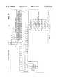
- start logic 36comprises a set of logic devices operationally coupled as shown in FIG. 2B.
- the start logic 36comprises conventional Xilinx library elements FDS, AND2B1, AND2B0 and OR2B1.
- the delay unit 38is preferably embodied within an RLD and is comprised of carry logic elements within a set of "n" CLBs 138, 144, 150, 154, where n is an integer.
- each carry logic elementcomprises high-speed carry-propagate circuitry.
- the delay unit 38additionally comprises a subset of the function generators within this set of n CLBs, to facilitate signal routing between the delay unit 38 and logic external to the delay unit 38, namely, the start logic 36, the pulse counter 40, and the sequence gate logic 42.
- the delay unit 38is implemented in a Xilinx XC4000 series FPGA through the use of "EXAMINE CI” and "FORCE CI” directives, corresponding to examining and forcing a carry-in signal, respectively.
- each CLB 138, 144, 150, 154adds a known delay (1.5 ns for a Xilinx XC4000 carry logic element and 4.5 ns for a Xilinx XC4000 F-type function generator) to the delay unit 38.
- the delay unit's 38 frequency of operationis preferably varied by either increasing or decreasing the number of carry logic elements connected in series. In the preferred embodiment, a maximal rate self-timed pulse sequencer 34 is desired.
- the number of CLBs 138, 144, 150, 154 comprising the delay unit 38is therefore dependent upon a slowest portion of the functional logic 24.
- n CLBs having a total delay equal to one-half "t" nspreferably comprises the delay unit 38.
- the delay of the delay unit 38may be dynamically varied during the course of the functional logic's 24 processing operations. This enables a first set of functional logic 24 operations to be performed at a first self-timed rate, a second set of functional logic 24 other operations to be performed at a second self-timed rate, and so on.
- function generator (1) 140receives the start pulse on line 35, and passes the pulse to carry logic element (1) 139. Carry logic element (1) 139 then passes the pulse over carry-out line 142 to a second CLB 144. Within the second CLB 144, carry logic element (2) 145 receives the pulse and passes it to function generator (2) 146, and also transfers the pulse over carry-out line 148 to a third CLB 150. Passing the pulse to function generator (2) 146 enables the pulse to be "tapped" from the delay unit 38 at that point so as to become the delay unit output signal 133 on line 39.
- a "tap"is defined as a coupling within the delay unit 38 that facilitates signal routing external to the delay unit 38.
- This "tapping"may alternatively occur at a different location within the delay unit 38 or may occur in several places, depending upon the set of functional logic 24 being implemented.
- the exact position within the delay unit 38 where line 39 is tappedis preferably chosen such that the signals generated on line 33 by the pulse sequencer are phase-aligned with respect to the external circuitry (not shown) that initiates the operation of the apparatus 20, as discussed with reference to FIG. 1.
- carry logic element (3) 151receives the pulse and passes it to a carry logic element within a next CLB, and so on until the pulse is passed to carry logic element (n) within an "nth" CLB 154.
- Any CLBs between the third CLB 150 and the "nth" CLB 154are preferably of the same construction and have preferably the same interface as the third CLB 150.
- function generator (3) 152is not required for the operation of the delay unit 38 because the third CLB 151 is not being tapped to route the pulse to a destination external to the delay unit 38. Thus, function generator (3) 152 may be advantageously used to implement part of the functional logic's 24 operations.
- carry logic element (n) 155receives the pulse and passes it to function generator (n) 156, which inverts the pulse and outputs the inverted pulse on line 37 as the feedback signal 132. It is via this pulse inversion that the self-timed oscillator transitions between logic "1" and logic "0.” Those skilled in the art will recognized that the pulse could have been inverted by function generator (1) 140 instead.
- the delay unit's 38 frequency of operationmay be varied by increasing or decreasing the number of carry logic elements coupled in series (i.e. by varying the value of "n"). In an alternate embodiment "n" could be zero, resulting in the start pulse, the feedback signal 132 and the delay unit output signal 133 becoming the same signal. In yet another alternate embodiment, the delay unit's 38 frequency of operation could be varied by additional signal routing through one or more function generators. In still another alternate embodiment, the delay unit's 38 frequency of operation could be modified or adjusted using signal routing resources within the RLD that have well-defined delay characteristics. Those skilled in the art will recognize that the delay unit 38 may be embodied in non-reconfigurable devices, using logic in which individual elements have a known maximum signal propagation delay.
- the pulse counter 40is comprised of a set of logic devices 160, 162, 164 (preferably created in a Xilinx XC4000 series FPGA using the library elements ROM16x1, FDR, and AND3B3) operationally coupled as shown in FIG. 2D.
- the ROMs 160are joined together with flip-flops 162 to implement the pulse count.
- a present state code Q3, Q2, Q1, Q0 of the flip-flops 162is used to produce the pulse count, with one present state code corresponding to the halt signal 134.
- the pulse counter 40increments until the Reset (1) pulse 105 is received on line 43.
- the codes to be stored in the ROM's 160are generated from the following present-state/next-state table:
- sequence gate logic 42is comprised of a set of logic devices (preferably partially created in a Xilinx XC4000 series FPGA using the library elements D3 -- 8E, AND2B1, FD, FD -- 1, NOR2, OR8, and OR7) operationally coupled as shown in FIG. 2E.
- the sequence gate logic 42decodes eight states using a set of glitch guardian circuits 170, as shown in FIG. 2E.
- the decodingis temporally in order of the pulse count on line 44.
- the last pulse count statei.e. (0, 0, 0) is decoded exactly one time.
- the CLKs 46, 47, 48, 48are generated by "ORing" the outputs of the set of glitch guardian circuits 170.
- sequence gate logic 42replaces the wired-ORs with wired-ANDs gates by using a DeMorganization of the local state decoders.
- the preferred sequence gate logic 42includes an even number of negative-edge triggered flip-flops and positive-edge triggered flip-flops, affording a highly efficient dual flip-flop per CLB packaging strategy, where like-clocked flip-flops are conjoined.
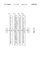
- the functional logic 24comprises a multiplexor (MUX) 50, a partial product generator (PPG) 52, a partial product summer (PPS) 54 and a product accumulator (PA) 56.
- the MUX 50receives the X-bit multiplicand on line 21 and outputs an S-bit multiplicand subset in response to the pulse count on line 44, as described in detail with reference to FIG. 4 below.
- the PPG 52multiplies the Y-bit multiplier on line 23 with the S-bit multiplicand subset and outputs a set of partial products to the PPS 54, as described in detail with reference to FIG. 5 below.
- the PPS 54combines the set of partial products and outputs a partial product sum to the PA 56 in response to the PPS-CLK 98 on line 46, as described in detail with reference to FIG. 6 below.
- the PA 56receives a Reset(2) pulse 107 (ref. FIG. 8) on line 45 from the start logic 36, and in response resets its internal flip-flops (FFs) to zero. Prior to the receipt of this Reset(2) pulse 107, a previous P-bit product remains on line 25.
- the PA 56generates a product accumulation by adding the partial product sum to a subset of the product accumulation's bits and outputs a P-bit product on line 25 in response to the PA-CLK(1, 2, 3) 99, 100, 101 (ref. FIG.
- a complete X-bit by Y-bit multiplicationis performed by the functional logic 24 after each S-bit multiplicand subset has been multiplied by the Y-bit multiplier and accumulated by the PA 56.
- the MUX 50is comprised of a first MUX 58 and a second MUX 60.
- Each MUX 58, 60is coupled to the input buffer 22 via line 21, such that each receives half of the X-bit multiplicand.
- the first MUX 58receives the even multiplicand bits (i.e. 2 0 , 2 2 , . . . 2 14 for a 16-bit multiplicand), while, the second MUX 60 receives the odd multiplicand bits (i.e. 2 1 , 2 3 , . . . 2 15 for a 16-bit multiplicand).
- Each MUX 58, 60receives the pulse count over line 44.
- the pulse countis incremented from the initial pulse count up to and including the largest pulse count.
- the initial pulse countpreferably corresponds to (0, 0, 1) on the line 44, where "1" is the LSB, and the largest pulse count preferably corresponds to (0, 0, 0).
- the pulse countthus preferably transitions from (0, 0, 1) to (0, 1, 0), (0, 1, 1), (1, 0, 0), (1, 0, 1), (1, 1, 0), (1, 1, 1), and then (0, 0, 0).
- the first and second MUX's 58, 60output an S-bit multiplicand subset to the PPG 52.
- a 2-bit multiplicand subset(2 i and 2 i+1 ) is sent to the PPG 52, where bit 2 i is selected from the first MUX 58 and bit 2 i+1 is selected from the second MUX 60.
- "S"equals "2" and "i” is an integer which preferably ranges from zero to fourteen as the pulse count ranges from (0, 0, 1) to (0, 0, 0).
- the PPG 52is comprised of a first set of partial product multipliers (PPMs) 51 and a second set of PPMs 53 whose inputs are coupled to receive the S-bit multiplicand subset from the first and second MUXs 58, 60 and the Y-bit multiplier on line 23. Outputs from the first and second set of PPMs 51, 53 are coupled to the PPS 54. For a 16-bit by 16-bit multiplication, each set of PPMs 51, 53 comprises four 2-bit by 2-bit PPMs operating in parallel, resulting in a total of 32-bits being sent to the PPS 54 after each multiplication operation.
- PPMspartial product multipliers
- Each 2-bit multiplier pair from the 16-bit multiplier on line 23is routed to one of the eight PPMs and is held constant during each partial product multiplication operation.
- one 2-bit multiplicand subseti.e. 2 i and 2 i+1
- bit 2 0is the least significant bit (LSB) and bit 2 17 is the most significant bit (MSB).
- the PPS 54comprises a PPS-adder 64, a PPS-incrementer 66, and a set of PPS-flip-flops 68.
- the PPS 54is coupled to receive the two partial products generated by the PPG 52.
- the PPS 54adds the two partial products and generates a partial product sum.
- the two LSBs (2 0 -2 1 ) from the first set of PPMs 51are received directly by the PPS-flip-flops 68; the PPS-adder 64 adds 14 bits (2 2 -2 15 ) from both the first and second set of PPMs 51, 53; the PPS-incrementer 66 accepts the two MSBs (2 16 -2 17 ) from the second set of PPMs 53 and a carry-out from the 14-bit PPS-adder 64; and an 18-bit partial product sum (2 0 -2 17 ) is generated and output.
- the partial product sum resulting from the additionis stored within the PPS-flip-flops 68 in response to a PPS-CLK 98 toggle on line 46.
- the PA 56comprises a PA-adder 70 coupled to receive the partial product sum from the PPS 54 and perform accumulations, a PA-incrementer 71, and a set of PA-flip-flops 72, 74, 76, 78, 80, 82, 84, 86, 88 for eventually storing the P-bit product.
- the PA-adder 70is a 16-bit adder
- the PA-incrementer 71is a 2-bit incrementer
- the set of PA-flip-flops 72, 74, 76, 78, 80, 82, 84, 86, 88comprise a first flip-flop set 72, a second flip-flop set 74, a third flip-flop set 76, a fourth flip-flop set 78, a fifth flip-flop set 80, a sixth flip-flop set 82, a seventh flip-flop set 84, an eighth flip-flop set 86, and a ninth flip-flop set 88 for storing a 32-bit product (p 0 -p 31 , where p 0 is the LSB and p 31 is the MSB).
- the two LSBs (2 0 -2 1 ) from a first partial product sum received from the PPS 54are stored in the second flip-flop set 74 in response to the rising edge of PA-CLK(1) 99 on line 47, thus becoming the 32-bit product's two LSBs (p 0 -p 1 ).
- a 16-bit product accumulation subset(bits 2 2 through 2 17 from the output of the 16-bit adder 70 and the 2-bit incrementer 71) is stored in the first flip-flop set 72 in response to the rising edge of PA-CLK(2) 100 on line 48.
- the 16-bit adder 70adds bits 2 0 through 2 15 of each partial product sum received from the PPS 54 to the 16-bit product accumulation subset to produce a product accumulation (bits 2 0 through 2 17 from the output of the 16-bit adder 70 and the 2-bit incrementer 71). Bits 2 2 through 2 17 of each product accumulation then become the product accumulation subset which is fed-back to the first flip-flop set 72, while product accumulation bits 2 0 and 2 1 are sequentially shifted after each product accumulation through the third through ninth flip flop sets 76, 78, 80, 82, 84, 86, 88 in response to a rising edge of the PA-CLK(3) 101 on line 49.
- bits p 0 and p 1are stored in the second flip-flop set 74; after eight PA-CLK(2) 100 toggles, bits p 16 through p 31 are stored in the first flip-flop set 72; and after seven PA-CLK(3) 101 toggles, bits p 2 and p 3 are stored in the ninth flip-flop set 88, bits p 4 and p 5 are stored in the eighth flip-flop set 86, bits p 6 and p 7 are stored in the seventh flip-flop set 84, bits p 8 and p 9 are stored in the sixth flip-flop set 82, bits p 10 and p 11 are stored in the fifth flip-flop set 80, bits p 12 and p 13 are stored in the fourth flip-flop set 78, and bits p 14 and p 15 are stored in the third flip-flop set 76.
- the 32-bit product(bits p 0 through p 31 ) is then sent to the output buffer 26 over line 25.
- the timing diagram 89is comprised of a start signal 90, a QStart signal 128, a Start Pulse signal 130, a Feedback signal 132, a delay unit output signal 133, a halt signal 134, a RESET(1) signal 91, a MUX(0) signal 92, a MUX(1) signal 94, a MUX(2) signal 96, a PPS-CLK signal 98, a RESET(2) signal 97, a PA-CLK(1) signal 99, a PA-CLK(2) signal 100, a PA-CLK(3) signal 101, a product signal 102, a first start signal 104, a next start signal 106, a first PPS-CLK signal 108, a first PA-CLK(1) signal 109, a first PA-CLK(2)
- the first start signal 104is received by the pulse sequencer 34 over line 32 as was shown in FIG. 2A.
- the start logic 36initializes the MUX(0) 92 (the LSB), MUX(1) 94 and MUX(2) 96 (the MSB) signals respectively to (0, 0, 1) by sending the Reset(1) pulse 105 over line 43 and sending the MUX(0) 92, MUX(1) 94 and MUX(2) signals to the MUX 50 over line 44.
- the MUX 50selects the first 2-bit multiplicand pair (2 0 -2 1 ) for a 16-bit by 16-bit multiplication, as is discussed above.
- the sequence gate logic 42delays sending out the first PPS-CLK signal 108 to the PPS 54 until a first 18-bit partial product sum is present at the PPS-flip-flops' 68 inputs. After the first 18-bit partial product sum has been stored in the PPS-flip-flops 68, the MUX(0) 92, MUX(1) 94 and MUX(2) signals are incremented to a next state (i.e. (0, 1, 0)) in preparation for a next 18-bit partial product sum. The sequence gate logic 42 also delays sending out the first PA-CLK(1) signal 109 over line 47 until the first 18-bit partial product sum is present at the second flip-flop set's 74 inputs.
- the start logic 36Just before the PA-CLK(1) pulse 109 is sent over line 47, the start logic 36 generates the Reset(2) pulse 107 over line 45 to clear out the previous P-bit PRODUCT 102.
- the PA-CLK(1) 99is toggled once per each complete 16-bit by 16-bit multiplication operation.
- the first PA-CLK(2) signal 110 over line 48is generated only after a first 16-bit product accumulation subset is present at the first flip-flop set's 72 inputs, after which the PA-CLK(2) 100 is toggled each time a next 16-bit product accumulation subset is present at the first flip-flop set's 72 inputs.
- the PA-CLK(2) 100is toggled eight times per each complete 16-bit by 16-bit multiplication operation.
- the first PA-CLK(3) signal 112 over line 49is generated only after a second 18-bit product accumulation is present at the third flip-flop set's 76 inputs, after which the PA-CLK(3) 101 is toggled each time a next 18-bit product accumulation is present at the third flip-flop set's 72 inputs.
- the PA-CLK(3) 101is toggled seven times per each complete 16-bit by 16-bit multiplication operation. Due to the known propagation delays present in a physical device embodying the present invention, the PRODUCT 102 will be known to be calculated within the product calculation time 114. As a result, an earliest time after the first start signal 104 that the second start signal 106 may be sent to the pulse sequencer 34 is after the PRODUCT signal 102 has stabilized. While only a 16-bit by 16-bit multiplication has been described, those skilled in the art will recognize that an X-bit by Y-bit multiplication may be effected in a similar manner.
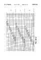
- FIG. 9Aa matrix of preferred partial product additions for a 16-bit by 16-bit multiplication performed by the present invention is shown.
- the PPS 54goes through eight summations and the PA 56 goes through seven accumulations, finally resulting in a 32-bit product output over line 25 to the output buffer 26, as discussed above.
- the LSBbeing 2 0 and the MSB being 2 31 .
- the portions of the matrix labeled "I, II, III, IV, V, VI, VII" and "VIII”an alignment of the eight partial product multipliers 62 within the PPG 52 is shown.
- portion "I" bits 2 0 and 2 1 of the 16-bit multiplicandare multiplied with the 16-bit multiplier; in portion “II” bits 2 2 and 2 3 of the 16-bit multiplicand are multiplied with the 16-bit multiplier; and so on until in portion "VIII" bits 2 14 and 2 15 of the 16-bit multiplicand are multiplied with the 16-bit multiplier.
- the PA 56adds all eight portions in the manner indicated within the matrix, resulting in the 32-bit product.
- FIG. 9Ba matrix of preferred partial product additions for an 8-bit by 8-bit multiplication performed in accordance with the present invention is shown.
- the PPS 54would be designed to go through four summations and the PA 56 through three accumulations, finally resulting in a 16-bit product output over line 25 to the output buffer 26, as discussed above.
- the LSBbeing 2 0
- the MSBbeing 2 15 .
- an alignment of the now four partial product multipliers 62 within the PPG 52is shown.
- portion "I" bits 2 0 and 2 1 of the 8-bit multiplicandare multiplied with the 8-bit multiplier; in portion “II” bits 2 2 and 2 3 of the 8-bit multiplicand are multiplied with the 8-bit multiplier; and so on until in portion "IV" bits 2 6 and 2 7 of the 8-bit multiplicand are multiplied with the 8-bit multiplier.
- the PA 56adds four portions in the manner indicated within the matrix, resulting in the 16-bit product.
- step 200a toggle from the reference clock while the input enable on line 29 is set to logic "1" causes the input buffer 22 to transfer the input data over lines 21 and 23 to the functional logic 24 inputs in synchrony with the reference clock toggle, in the manner described above.
- step 202and in response to the START signal's 90 transition from logic "0" to logic "1" on line 32, the pulse sequencer 34 generates a maximal-rate pulse sequence over line 33, for driving the functional logic 24 at a rate dependent upon an algorithm execution time for the functional logic 24 but independent of the reference clock on line 28.
- Step 202is described in detail in FIG. 11.
- step 204the functional logic 24 generates output data on line 25 in response to the maximal-rate pulse sequence on line 33. Step 204 is described in detail in FIG. 12.
- step 206the output data is transferred from the functional logic 24 over line 25 and into the output buffer 26 in synchrony with and in response to a toggle from the reference clock on line 28, while the output enable on line 31 is set to logic "1," as is described above. After step 206, the preferred method ends.
- step 250a flowchart of a preferred method for generating a pulse sequence (step 202 of FIG. 10) is shown.
- the preferred methodbegins in step 250 with the start logic 36 monitoring the state of the start signal 90 on line 32 and the halt signal on line 41.
- step 252if the start signal 90 transitions to logic "1" while the halt signal remains set to logic "0", then the method proceeds to step 254, else the method returns to step 250.
- the start logic 36initializes the pulse counter 40, as discussed above.
- step 255the start logic 36 transmits a start pulse to the delay unit 38, as described above.
- step 256the pulse counter 40 increments the pulse count signal (i.e.
- step 258the sequence gate logic 42 generates the PPS-CLK signal 98 and the PA-CLK signals 99, 100, 101 in response to the pulse count signal, in the manner described above.
- step 260if the pulse count signal is equal to a largest pulse count signal, then the method proceeds to step 262, else the method returns to step 256.
- step 262the pulse counter 40 stops transmitting start pulses to the delay unit 38 by setting the halt signal on line 41 to logic "1.” After step 262, the preferred method ends.
- step 300a flowchart of a preferred method for generating output data in response to the pulse sequence (step 204 of FIG. 12) is shown.
- the preferred methodbegins in step 300 with the MUX 50 inputting the X-bit multiplicand, the PPG 52 inputting the Y-bit multiplier, and the start logic 36 initializing the partial product sum and the product accumulation to zero, as described above.
- the MUX 50selects a next S-bit multiplicand subset, in the manner described above.
- step 304the PPG 52 multiplies a current S-bit multiplicand subset (i.e.
- the current subsetis the next subset that was selected in step 302) by the Y-bit multiplier to generate the partial products sent to the PPS 54 as described above.
- the PPS 54generates the partial product sum and sends it to the PA 56 in the manner described above.
- the PA 56adds the partial product sum to the product accumulation as described above.
- step 310if a next S-Bit Multiplicand Subset has yet to be multiplied with the Y-bit multiplier, the method returns to step 302, else the method proceeds to step 312.
- the PA 56outputs a P-bit product to the output buffer 26. After step 312, the preferred method ends.
- the present inventionis preferably used within the context of a computing system.
- circuits designed to provide high-speed implementations of particular algorithmsare constructed of multiple circuitry layers. Each circuitry layer receives a set of signals, performs a particular set of operations, and outputs a set of results in synchrony with a reference clock. Signals are transferred from one circuitry layer to another.
- Such prior art circuit designsoften require many circuitry layers, undesirably necessitating the use of a large number of hardware resources.
- the present inventionimplements an algorithm by reusing a minimal number of hardware resources over and over at a maximal, self-timed rate to generate a result.
- the present inventionprovides a means for implementing an algorithm using significantly fewer hardware resources than required by prior art high-speed circuits, without suffering from any significant result-generation rate penalty. This is particularly advantageous when implementing one or more versions of the present invention in an RLD.
- the present inventionis particularly advantageous in view of current asynchronous logic designs.
- the present inventiondoes not require the generation of "completion signals" upon completing operational tasks; has known and predictable completion times; does not require external clocking elements but instead has its own integral pulse sequencer timing element; has completion times which are data independent; may synchronously interface with external circuitry; can coherently phase data exchanges with external circuitry; only adds additional localized circuit complexity when delay is added to its timing elements; is very easy to encapsulate within synchronous external circuitry; and affects the performance of only a localized set of circuitry instead of an entire system of external circuitry.
- the delay unit 38could be designed to continuously recycle a pulse following RLD configuration, thereby eliminating the start logic 36.
- an RS flip-flopcould enable a multiplexor to pass the delay unit output signal to the pulse counter 40 and sequence gate logic 42 in response to the start signal.
- the functional logicis not limited to the case of a self-timed multiplier.
- the functional logiccould be modified to provide functions including, but not limited to, a self-timed divider, a self-timed convolver, or a self-timed signal processor. Variations upon and modifications to the preferred embodiments are provided for by the present invention, which is limited only by the following claims.
Landscapes
- Engineering & Computer Science (AREA)
- Theoretical Computer Science (AREA)
- Physics & Mathematics (AREA)
- General Engineering & Computer Science (AREA)
- General Physics & Mathematics (AREA)
- Logic Circuits (AREA)
- Advance Control (AREA)
- Data Exchanges In Wide-Area Networks (AREA)
- Tests Of Electronic Circuits (AREA)
- Pulse Circuits (AREA)
Abstract
Description
______________________________________ Present-State Next-State Q3 Q2 Q1 Q0 RD3 RD2 RD1 RD0 ______________________________________ 0 0 0 0 0 0 0 1 0 0 0 1 0 0 1 0 0 0 1 0 0 0 1 1 0 0 1 1 0 1 0 0 0 1 0 0 0 1 0 1 0 1 0 1 0 1 1 0 0 1 1 0 0 1 1 1 0 1 1 1 1 0 0 0 1 0 0 0 1 0 0 0 1 0 0 1 1 0 0 0 1 0 1 0 1 0 0 0 1 0 1 1 1 0 0 0 1 1 0 0 1 0 0 0 1 1 0 1 1 0 0 0 1 1 1 0 1 0 0 0 1 1 1 1 1 0 0 0 ______________________________________
Claims (21)
Priority Applications (4)
| Application Number | Priority Date | Filing Date | Title |
|---|---|---|---|
| US08/590,499US5854918A (en) | 1996-01-24 | 1996-01-24 | Apparatus and method for self-timed algorithmic execution |
| JP32321396AJP3784476B2 (en) | 1996-01-24 | 1996-12-03 | Timing signal generation method and apparatus |
| CN97102100.7ACN1103951C (en) | 1996-01-24 | 1997-01-23 | Device for executing self-timing algorithm and method thereof |
| DE19702326ADE19702326B4 (en) | 1996-01-24 | 1997-01-23 | Device and method for a self-timed algorithmic execution |
Applications Claiming Priority (1)
| Application Number | Priority Date | Filing Date | Title |
|---|---|---|---|
| US08/590,499US5854918A (en) | 1996-01-24 | 1996-01-24 | Apparatus and method for self-timed algorithmic execution |
Publications (1)
| Publication Number | Publication Date |
|---|---|
| US5854918Atrue US5854918A (en) | 1998-12-29 |
Family
ID=24362511
Family Applications (1)
| Application Number | Title | Priority Date | Filing Date |
|---|---|---|---|
| US08/590,499Expired - LifetimeUS5854918A (en) | 1996-01-24 | 1996-01-24 | Apparatus and method for self-timed algorithmic execution |
Country Status (4)
| Country | Link |
|---|---|
| US (1) | US5854918A (en) |
| JP (1) | JP3784476B2 (en) |
| CN (1) | CN1103951C (en) |
| DE (1) | DE19702326B4 (en) |
Cited By (59)
| Publication number | Priority date | Publication date | Assignee | Title |
|---|---|---|---|---|
| US6317842B1 (en)* | 1999-02-16 | 2001-11-13 | Qlogic Corporation | Method and circuit for receiving dual edge clocked data |
| US6526520B1 (en)* | 1997-02-08 | 2003-02-25 | Pact Gmbh | Method of self-synchronization of configurable elements of a programmable unit |
| US6542998B1 (en) | 1997-02-08 | 2003-04-01 | Pact Gmbh | Method of self-synchronization of configurable elements of a programmable module |
| US6675306B1 (en) | 2000-03-10 | 2004-01-06 | Ricoh Company Ltd. | Method and apparatus for phase-lock in a field programmable gate array (FPGA) |
| US6990555B2 (en) | 2001-01-09 | 2006-01-24 | Pact Xpp Technologies Ag | Method of hierarchical caching of configuration data having dataflow processors and modules having two- or multidimensional programmable cell structure (FPGAs, DPGAs, etc.) |
| US7003660B2 (en) | 2000-06-13 | 2006-02-21 | Pact Xpp Technologies Ag | Pipeline configuration unit protocols and communication |
| US7007114B1 (en) | 2003-01-31 | 2006-02-28 | Qlogic Corporation | System and method for padding data blocks and/or removing padding from data blocks in storage controllers |
| US7010667B2 (en) | 1997-02-11 | 2006-03-07 | Pact Xpp Technologies Ag | Internal bus system for DFPS and units with two- or multi-dimensional programmable cell architectures, for managing large volumes of data with a high interconnection complexity |
| US7028107B2 (en) | 1996-12-27 | 2006-04-11 | Pact Xpp Technologies Ag | Process for automatic dynamic reloading of data flow processors (DFPS) and units with two- or three- dimensional programmable cell architectures (FPGAS, DPGAS, and the like) |
| US7039771B1 (en) | 2003-03-10 | 2006-05-02 | Marvell International Ltd. | Method and system for supporting multiple external serial port devices using a serial port controller in embedded disk controllers |
| US7064915B1 (en) | 2003-03-10 | 2006-06-20 | Marvell International Ltd. | Method and system for collecting servo field data from programmable devices in embedded disk controllers |
| US7080188B2 (en) | 2003-03-10 | 2006-07-18 | Marvell International Ltd. | Method and system for embedded disk controllers |
| US7111228B1 (en) | 2002-05-07 | 2006-09-19 | Marvell International Ltd. | System and method for performing parity checks in disk storage system |
| US7120084B2 (en) | 2004-06-14 | 2006-10-10 | Marvell International Ltd. | Integrated memory controller |
| US7139150B2 (en) | 2004-02-10 | 2006-11-21 | Marvell International Ltd. | Method and system for head position control in embedded disk drive controllers |
| US7174443B1 (en) | 1996-12-20 | 2007-02-06 | Pact Xpp Technologies Ag | Run-time reconfiguration method for programmable units |
| US7210129B2 (en) | 2001-08-16 | 2007-04-24 | Pact Xpp Technologies Ag | Method for translating programs for reconfigurable architectures |
| US7237087B2 (en) | 1996-12-09 | 2007-06-26 | Pact Xpp Technologies Ag | Reconfigurable multidimensional array processor allowing runtime reconfiguration of selected individual array cells |
| US7240267B2 (en) | 2004-11-08 | 2007-07-03 | Marvell International Ltd. | System and method for conducting BIST operations |
| US7266725B2 (en) | 2001-09-03 | 2007-09-04 | Pact Xpp Technologies Ag | Method for debugging reconfigurable architectures |
| US7287102B1 (en) | 2003-01-31 | 2007-10-23 | Marvell International Ltd. | System and method for concatenating data |
| US7386661B2 (en) | 2004-10-13 | 2008-06-10 | Marvell International Ltd. | Power save module for storage controllers |
| US7394284B2 (en) | 2002-09-06 | 2008-07-01 | Pact Xpp Technologies Ag | Reconfigurable sequencer structure |
| US7434191B2 (en) | 2001-09-03 | 2008-10-07 | Pact Xpp Technologies Ag | Router |
| US7444531B2 (en) | 2001-03-05 | 2008-10-28 | Pact Xpp Technologies Ag | Methods and devices for treating and processing data |
| US7492545B1 (en) | 2003-03-10 | 2009-02-17 | Marvell International Ltd. | Method and system for automatic time base adjustment for disk drive servo controllers |
| US7526691B1 (en) | 2003-10-15 | 2009-04-28 | Marvell International Ltd. | System and method for using TAP controllers |
| US7577822B2 (en) | 2001-12-14 | 2009-08-18 | Pact Xpp Technologies Ag | Parallel task operation in processor and reconfigurable coprocessor configured based on information in link list including termination information for synchronization |
| US7581076B2 (en) | 2001-03-05 | 2009-08-25 | Pact Xpp Technologies Ag | Methods and devices for treating and/or processing data |
| US7595659B2 (en) | 2000-10-09 | 2009-09-29 | Pact Xpp Technologies Ag | Logic cell array and bus system |
| US7609468B2 (en) | 2005-04-06 | 2009-10-27 | Marvell International Ltd. | Method and system for read gate timing control for storage controllers |
| US7650448B2 (en) | 1996-12-20 | 2010-01-19 | Pact Xpp Technologies Ag | I/O and memory bus system for DFPS and units with two- or multi-dimensional programmable cell architectures |
| US7657861B2 (en) | 2002-08-07 | 2010-02-02 | Pact Xpp Technologies Ag | Method and device for processing data |
| US7657877B2 (en) | 2001-06-20 | 2010-02-02 | Pact Xpp Technologies Ag | Method for processing data |
| US7757009B2 (en) | 2004-07-19 | 2010-07-13 | Marvell International Ltd. | Storage controllers with dynamic WWN storage modules and methods for managing data and connections between a host and a storage device |
| US7802026B2 (en) | 2004-11-15 | 2010-09-21 | Marvell International Ltd. | Method and system for processing frames in storage controllers |
| US7822881B2 (en) | 1996-12-27 | 2010-10-26 | Martin Vorbach | Process for automatic dynamic reloading of data flow processors (DFPs) and units with two- or three-dimensional programmable cell architectures (FPGAs, DPGAs, and the like) |
| US7844796B2 (en) | 2001-03-05 | 2010-11-30 | Martin Vorbach | Data processing device and method |
| US7870346B2 (en) | 2003-03-10 | 2011-01-11 | Marvell International Ltd. | Servo controller interface module for embedded disk controllers |
| US7996827B2 (en) | 2001-08-16 | 2011-08-09 | Martin Vorbach | Method for the translation of programs for reconfigurable architectures |
| US8032674B2 (en) | 2004-07-19 | 2011-10-04 | Marvell International Ltd. | System and method for controlling buffer memory overflow and underflow conditions in storage controllers |
| US8058899B2 (en) | 2000-10-06 | 2011-11-15 | Martin Vorbach | Logic cell array and bus system |
| US8127061B2 (en) | 2002-02-18 | 2012-02-28 | Martin Vorbach | Bus systems and reconfiguration methods |
| US8156284B2 (en) | 2002-08-07 | 2012-04-10 | Martin Vorbach | Data processing method and device |
| US8166217B2 (en) | 2004-06-28 | 2012-04-24 | Marvell International Ltd. | System and method for reading and writing data using storage controllers |
| US8230411B1 (en) | 1999-06-10 | 2012-07-24 | Martin Vorbach | Method for interleaving a program over a plurality of cells |
| US8250503B2 (en) | 2006-01-18 | 2012-08-21 | Martin Vorbach | Hardware definition method including determining whether to implement a function as hardware or software |
| US8281108B2 (en) | 2002-01-19 | 2012-10-02 | Martin Vorbach | Reconfigurable general purpose processor having time restricted configurations |
| US8473911B1 (en) | 2010-07-23 | 2013-06-25 | Xilinx, Inc. | Documentation generation from a computer readable symbolic representation |
| US8686549B2 (en) | 2001-09-03 | 2014-04-01 | Martin Vorbach | Reconfigurable elements |
| US8686475B2 (en) | 2001-09-19 | 2014-04-01 | Pact Xpp Technologies Ag | Reconfigurable elements |
| US8812820B2 (en) | 2003-08-28 | 2014-08-19 | Pact Xpp Technologies Ag | Data processing device and method |
| US8819505B2 (en) | 1997-12-22 | 2014-08-26 | Pact Xpp Technologies Ag | Data processor having disabled cores |
| US8914590B2 (en) | 2002-08-07 | 2014-12-16 | Pact Xpp Technologies Ag | Data processing method and device |
| US9037807B2 (en) | 2001-03-05 | 2015-05-19 | Pact Xpp Technologies Ag | Processor arrangement on a chip including data processing, memory, and interface elements |
| US9201599B2 (en) | 2004-07-19 | 2015-12-01 | Marvell International Ltd. | System and method for transmitting data in storage controllers |
| US20170366177A1 (en)* | 2014-09-25 | 2017-12-21 | Taiwan Semiconductor Manufacturing Company, Ltd. | Integrated circuit and method of testing |
| US20190205236A1 (en)* | 2017-12-29 | 2019-07-04 | Intel Corporation | Device, system and method for identifying a source of latency in pipeline circuitry |
| US10950299B1 (en) | 2014-03-11 | 2021-03-16 | SeeQC, Inc. | System and method for cryogenic hybrid technology computing and memory |
Citations (30)
| Publication number | Priority date | Publication date | Assignee | Title |
|---|---|---|---|---|
| US3222536A (en)* | 1961-02-02 | 1965-12-07 | Burroughs Corp | Time-controlled logical circuit |
| US3358128A (en)* | 1964-08-31 | 1967-12-12 | Burroughs Corp | Delay line arithmetic circuit |
| US3553446A (en)* | 1966-08-04 | 1971-01-05 | Honeywell Inc | Carry determination logic |
| US4322643A (en)* | 1980-04-28 | 1982-03-30 | Rca Corporation | Digital phase comparator with improved sensitivity for small phase differences |
| US4682303A (en)* | 1983-09-05 | 1987-07-21 | Matsushita Electric Industrial Co., Ltd. | Parallel binary adder |
| US4707800A (en)* | 1985-03-04 | 1987-11-17 | Raytheon Company | Adder/substractor for variable length numbers |
| US4737926A (en)* | 1986-01-21 | 1988-04-12 | Intel Corporation | Optimally partitioned regenerative carry lookahead adder |
| US4841468A (en)* | 1987-03-20 | 1989-06-20 | Bipolar Integrated Technology, Inc. | High-speed digital multiplier architecture |
| US4876660A (en)* | 1987-03-20 | 1989-10-24 | Bipolar Integrated Technology, Inc. | Fixed-point multiplier-accumulator architecture |
| US4972362A (en)* | 1988-06-17 | 1990-11-20 | Bipolar Integrated Technology, Inc. | Method and apparatus for implementing binary multiplication using booth type multiplication |
| US4982352A (en)* | 1988-06-17 | 1991-01-01 | Bipolar Integrated Technology, Inc. | Methods and apparatus for determining the absolute value of the difference between binary operands |
| US5018093A (en)* | 1990-01-02 | 1991-05-21 | Ibm Corporation | High performance self-checking adder having small circuit area |
| US5038117A (en)* | 1990-01-23 | 1991-08-06 | Hewlett-Packard Company | Multiple-modulator fractional-N divider |
| US5047975A (en)* | 1987-11-16 | 1991-09-10 | Intel Corporation | Dual mode adder circuitry with overflow detection and substitution enabled for a particular mode |
| US5109394A (en)* | 1990-12-24 | 1992-04-28 | Ncr Corporation | All digital phase locked loop |
| US5117386A (en)* | 1984-04-24 | 1992-05-26 | U.S. Philips Corporation | Full adder circuit |
| US5153848A (en)* | 1988-06-17 | 1992-10-06 | Bipolar Integrated Technology, Inc. | Floating point processor with internal free-running clock |
| US5173617A (en)* | 1988-06-27 | 1992-12-22 | Motorola, Inc. | Digital phase lock clock generator without local oscillator |
| US5175453A (en)* | 1990-08-15 | 1992-12-29 | Lsi Logic Corporation | Configurable pulse generator, especially for implementing signal delays in semiconductor devices |
| US5450607A (en)* | 1993-05-17 | 1995-09-12 | Mips Technologies Inc. | Unified floating point and integer datapath for a RISC processor |
| US5483478A (en)* | 1992-10-16 | 1996-01-09 | Xilinx, Inc. | Method and structure for reducing carry delay for a programmable carry chain |
| US5502403A (en)* | 1994-12-20 | 1996-03-26 | Cypress Semiconductor Corp. | High speed configuration independent programmable macrocell |
| US5509040A (en)* | 1993-07-23 | 1996-04-16 | Mitsubishi Denki Kabushiki Kaisha | Frequency divider |
| US5511181A (en)* | 1993-04-26 | 1996-04-23 | Apple Computer, Inc. | Polycyclic timing system and apparatus for pipelined computer operation |
| US5511173A (en)* | 1989-11-08 | 1996-04-23 | Ricoh Co., Ltd. | Programmable logic array and data processing unit using the same |
| US5553276A (en)* | 1993-06-30 | 1996-09-03 | International Business Machines Corporation | Self-time processor with dynamic clock generator having plurality of tracking elements for outputting sequencing signals to functional units |
| US5566079A (en)* | 1992-11-12 | 1996-10-15 | Vlsi Technology, Inc. | Parameterized generic multiplier complier |
| US5566123A (en)* | 1995-02-10 | 1996-10-15 | Xilinx, Inc. | Synchronous dual port ram |
| US5576982A (en)* | 1994-10-17 | 1996-11-19 | Unisys Corporation | Fast significant bit calculator and its application to integer multiplication and division |
| US5710910A (en)* | 1994-09-30 | 1998-01-20 | University Of Washington | Asynchronous self-tuning clock domains and method for transferring data among domains |
- 1996
- 1996-01-24USUS08/590,499patent/US5854918A/ennot_activeExpired - Lifetime
- 1996-12-03JPJP32321396Apatent/JP3784476B2/ennot_activeExpired - Fee Related
- 1997
- 1997-01-23DEDE19702326Apatent/DE19702326B4/ennot_activeExpired - Fee Related
- 1997-01-23CNCN97102100.7Apatent/CN1103951C/ennot_activeExpired - Fee Related
Patent Citations (30)
| Publication number | Priority date | Publication date | Assignee | Title |
|---|---|---|---|---|
| US3222536A (en)* | 1961-02-02 | 1965-12-07 | Burroughs Corp | Time-controlled logical circuit |
| US3358128A (en)* | 1964-08-31 | 1967-12-12 | Burroughs Corp | Delay line arithmetic circuit |
| US3553446A (en)* | 1966-08-04 | 1971-01-05 | Honeywell Inc | Carry determination logic |
| US4322643A (en)* | 1980-04-28 | 1982-03-30 | Rca Corporation | Digital phase comparator with improved sensitivity for small phase differences |
| US4682303A (en)* | 1983-09-05 | 1987-07-21 | Matsushita Electric Industrial Co., Ltd. | Parallel binary adder |
| US5117386A (en)* | 1984-04-24 | 1992-05-26 | U.S. Philips Corporation | Full adder circuit |
| US4707800A (en)* | 1985-03-04 | 1987-11-17 | Raytheon Company | Adder/substractor for variable length numbers |
| US4737926A (en)* | 1986-01-21 | 1988-04-12 | Intel Corporation | Optimally partitioned regenerative carry lookahead adder |
| US4876660A (en)* | 1987-03-20 | 1989-10-24 | Bipolar Integrated Technology, Inc. | Fixed-point multiplier-accumulator architecture |
| US4841468A (en)* | 1987-03-20 | 1989-06-20 | Bipolar Integrated Technology, Inc. | High-speed digital multiplier architecture |
| US5047975A (en)* | 1987-11-16 | 1991-09-10 | Intel Corporation | Dual mode adder circuitry with overflow detection and substitution enabled for a particular mode |
| US4972362A (en)* | 1988-06-17 | 1990-11-20 | Bipolar Integrated Technology, Inc. | Method and apparatus for implementing binary multiplication using booth type multiplication |
| US4982352A (en)* | 1988-06-17 | 1991-01-01 | Bipolar Integrated Technology, Inc. | Methods and apparatus for determining the absolute value of the difference between binary operands |
| US5153848A (en)* | 1988-06-17 | 1992-10-06 | Bipolar Integrated Technology, Inc. | Floating point processor with internal free-running clock |
| US5173617A (en)* | 1988-06-27 | 1992-12-22 | Motorola, Inc. | Digital phase lock clock generator without local oscillator |
| US5511173A (en)* | 1989-11-08 | 1996-04-23 | Ricoh Co., Ltd. | Programmable logic array and data processing unit using the same |
| US5018093A (en)* | 1990-01-02 | 1991-05-21 | Ibm Corporation | High performance self-checking adder having small circuit area |
| US5038117A (en)* | 1990-01-23 | 1991-08-06 | Hewlett-Packard Company | Multiple-modulator fractional-N divider |
| US5175453A (en)* | 1990-08-15 | 1992-12-29 | Lsi Logic Corporation | Configurable pulse generator, especially for implementing signal delays in semiconductor devices |
| US5109394A (en)* | 1990-12-24 | 1992-04-28 | Ncr Corporation | All digital phase locked loop |
| US5483478A (en)* | 1992-10-16 | 1996-01-09 | Xilinx, Inc. | Method and structure for reducing carry delay for a programmable carry chain |
| US5566079A (en)* | 1992-11-12 | 1996-10-15 | Vlsi Technology, Inc. | Parameterized generic multiplier complier |
| US5511181A (en)* | 1993-04-26 | 1996-04-23 | Apple Computer, Inc. | Polycyclic timing system and apparatus for pipelined computer operation |
| US5450607A (en)* | 1993-05-17 | 1995-09-12 | Mips Technologies Inc. | Unified floating point and integer datapath for a RISC processor |
| US5553276A (en)* | 1993-06-30 | 1996-09-03 | International Business Machines Corporation | Self-time processor with dynamic clock generator having plurality of tracking elements for outputting sequencing signals to functional units |
| US5509040A (en)* | 1993-07-23 | 1996-04-16 | Mitsubishi Denki Kabushiki Kaisha | Frequency divider |
| US5710910A (en)* | 1994-09-30 | 1998-01-20 | University Of Washington | Asynchronous self-tuning clock domains and method for transferring data among domains |
| US5576982A (en)* | 1994-10-17 | 1996-11-19 | Unisys Corporation | Fast significant bit calculator and its application to integer multiplication and division |
| US5502403A (en)* | 1994-12-20 | 1996-03-26 | Cypress Semiconductor Corp. | High speed configuration independent programmable macrocell |
| US5566123A (en)* | 1995-02-10 | 1996-10-15 | Xilinx, Inc. | Synchronous dual port ram |
Non-Patent Citations (52)
| Title |
|---|
| Abstracts on Automatic layout synthesis of leaf cells, High performance disk I/O in a bus based system, Access graph: a model for investigating memory consistency, Probe acquisition for the MSPARC hybrid monitor, An adaptive and fault tolerant wormhole routing strategy for k ary n cubes & A performance monitor for the MSPARC multicomputer.* |
| Abstracts on Automatic layout synthesis of leaf cells, High-performance disk I/O in a bus-based system, Access graph: a model for investigating memory consistency, Probe acquisition for the MSPARC hybrid monitor, An adaptive and fault tolerant wormhole routing strategy for k-ary n-cubes & A performance monitor for the MSPARC multicomputer. |
| Brown, Chappell, "Fourier transform ported to PFGAs" Electronic Engineering Times, Nov. 13, 1995 pp. 53-54. |
| Brown, Chappell, Fourier transform ported to PFGAs Electronic Engineering Times, Nov. 13, 1995 pp. 53 54.* |
| Calvo,J. Acha J.I. and Valencia M, "Asynchronous Modular Arbiter" IEEE Transactions on Computers, vol. C-35, No. 1, Jan. 1986 pp. 67-70. |
| Calvo,J. Acha J.I. and Valencia M, Asynchronous Modular Arbiter IEEE Transactions on Computers, vol. C 35, No. 1, Jan. 1986 pp. 67 70.* |
| Chapiro, Daniel M, "Reliable High-Speed Arbitration and Synchronization" IEEE Transactions of Computers, vol. C-36, No. 10, Oct. 1987 pp. 1251-1255. |
| Chapiro, Daniel M, Reliable High Speed Arbitration and Synchronization IEEE Transactions of Computers, vol. C 36, No. 10, Oct. 1987 pp. 1251 1255.* |
| E Mail Correspondence, M. Baxter eworld.com Wed Oct 18 22:13:15 1995.* |
| Efendovich, Avner et al., "Multi-Frequency Zero-Jitter Delay-Locked Loop", IEEE 1993 Custom Integrated Circuits Conference, 1993, pp. 27.1.1-27.1.4. |
| Efendovich, Avner et al., Multi Frequency Zero Jitter Delay Locked Loop , IEEE 1993 Custom Integrated Circuits Conference, 1993, pp. 27.1.1 27.1.4.* |
| E-Mail Correspondence, M. Baxter@eworld.com Wed Oct 18 22:13:15 1995. |
| Guibaly, Fayez El "Design and Analysis of Arbitration Protocols" IEEE Trasactions on Computers, vol. 38, No. 2, Feb. 1989 pp. 161-171. |
| Guibaly, Fayez El Design and Analysis of Arbitration Protocols IEEE Trasactions on Computers, vol. 38, No. 2, Feb. 1989 pp. 161 171.* |
| Horowitz, Mark et al., "TP 10.5 PLL Design for a 500 MB/s Interface", 1993 IEEE International Solid-State Circuite Conference/Digest of Technical Papers, 1993, pp. 160 & 161. |
| Horowitz, Mark et al., TP 10.5 PLL Design for a 500 MB/s Interface , 1993 IEEE International Solid State Circuite Conference/Digest of Technical Papers, 1993, pp. 160 & 161.* |
| IEEE Computer Society Technical Committee on Computer Architecture Newsletter, Oct. 1995. Special issue on Asynchronous Computer Architecture pp. 1 44.* |
| IEEE Computer Society Technical Committee on Computer Architecture Newsletter, Oct. 1995. Special issue on Asynchronous Computer Architecture pp. 1-44. |
| Internet Search on Term: "Asynchronous Systems Research Group" Feb. 1, 1996, pp. 1-3. |
| Internet Search on Term: Asynchronous Systems Research Group Feb. 1, 1996, pp. 1 3.* |
| Johnson, Mark, G. and Hudson, Edwin L., "A Variable Delay Line PLL for CPU-Coprocessor Synchronization", IEEE Journal Of Solid-State Circuits, vol. 23, No. 5 Oct. 1988, pp. 1218-1223. |
| Johnson, Mark, G. and Hudson, Edwin L., A Variable Delay Line PLL for CPU Coprocessor Synchronization , IEEE Journal Of Solid State Circuits, vol. 23, No. 5 Oct. 1988, pp. 1218 1223.* |
| Lee, Thomas, H. et al., "a 2.5 V CMOS Delay-Locked Loop for an 18 Mbit, 500 Megabyte/s DRAM", IEEE Journal of Solid-State Circuits, vol. 29, No. 12, Dec. 1994, pp. 1491-1496. |
| Lee, Thomas, H. et al., a 2.5 V CMOS Delay Locked Loop for an 18 Mbit, 500 Megabyte/s DRAM , IEEE Journal of Solid State Circuits, vol. 29, No. 12, Dec. 1994, pp. 1491 1496.* |
| Linder, Daniel, H., "Phase Logic: Supporting the Synchronous Design Paradigm with Delay-Insensitive Circuitry". |
| Linder, Daniel, H., Phase Logic: Supporting the Synchronous Design Paradigm with Delay Insensitive Circuitry .* |
| Listing of miscellaneous reference text.* |
| Mahewsaran, Kapilan, "Implementing Self-Timed Circuits in Field Programmable Gate Arrays" Thesis for Master of Science in Electrical and Computer Engineering, Office of Graduate Studies, University of California, Davis. 1995 pp. 1-80. |
| Mahewsaran, Kapilan, Implementing Self Timed Circuits in Field Programmable Gate Arrays Thesis for Master of Science in Electrical and Computer Engineering, Office of Graduate Studies, University of California, Davis. 1995 pp. 1 80.* |
| McConnel, Stephen R. And Sieworek, Daniel P., "Synchronizationand Voting" IEEE Transactions on Computers, vol. C-30, No. 2, Feb. 1981 pp. 161-164. |
| McConnel, Stephen R. And Sieworek, Daniel P., Synchronizationand Voting IEEE Transactions on Computers, vol. C 30, No. 2, Feb. 1981 pp. 161 164.* |
| Meng, Teresa H., Synchronization Design for Digital Systems pp. 92 118.* |
| Meng, Teresa H., Synchronization Design for Digital Systems pp. 92-118. |
| Novak, Joe H. and Brunvand, Erik, "Using FPGAs to Prototype a Self-Timed Floating Point Co-Processor," 1994 IEEE Custom Integrated Circuits Conference, pp. 85-88. |
| Novak, Joe H. and Brunvand, Erik, Using FPGAs to Prototype a Self Timed Floating Point Co Processor, 1994 IEEE Custom Integrated Circuits Conference, pp. 85 88.* |
| Payne, Rob, Dept. Of Computer Science, University of Edinburgh, "Self-Timed FPGA Systems" pp. 1-12. |
| Payne, Rob, Dept. Of Computer Science, University of Edinburgh, Self Timed FPGA Systems pp. 1 12.* |
| Pechoucek,Miroslav "Anamalous Response Times of Input Synchronizers" IEEE Transactions on Computers, vol. C-25, No. 2, Feb. 1976 pp. 133-139. |
| Pechoucek,Miroslav Anamalous Response Times of Input Synchronizers IEEE Transactions on Computers, vol. C 25, No. 2, Feb. 1976 pp. 133 139.* |
| Professor Vankatesh Akella, "Asynchronous Systems Research Group", Department of Electrical and Computer Engineering, University of California, Davis, akella@ece.ucdavis.edu. |
| Professor Vankatesh Akella, Asynchronous Systems Research Group , Department of Electrical and Computer Engineering, University of California, Davis, akella ece.ucdavis.edu.* |
| Rosenberger, Fred, "Q-Modules: Internally Clocked Delay-Insensitive Modules" IEEE Transactions on Computers, vol. 37, No. 9, Sep. 1988 pp. 1005-1017. |
| Rosenberger, Fred, Q Modules: Internally Clocked Delay Insensitive Modules IEEE Transactions on Computers , vol. 37, No. 9, Sep. 1988 pp. 1005 1017.* |
| Unger, Stephen H., "Asynchronous Sequential Switching Circuits", Krieger Publishing Co. Inc. 1983, pp. 118-253. |
| Unger, Stephen H., Asynchronous Sequential Switching Circuits , Krieger Publishing Co. Inc. 1983, pp. 118 253.* |
| Waizman, Alex, "FA18.5: A Delay Line Loop for Frequency Synthesis of De-Skewed Clock", 1994 IEEE International Solid-State Circuite Conference/Digest of Technical Papers, 1994, pp. 298 & 299. |
| Waizman, Alex, FA18.5: A Delay Line Loop for Frequency Synthesis of De Skewed Clock , 1994 IEEE International Solid State Circuite Conference/Digest of Technical Papers, 1994, pp. 298 & 299.* |
| Wilkinson, Barry "Comments on Design and Analysis of Arbitration Protocols" IEEE Transactions on Computers vol. 41, No. 3, Mar. 1992 pp. 348-351. |
| Wilkinson, Barry Comments on Design and Analysis of Arbitration Protocols IEEE Transactions on Computers vol. 41, No. 3, Mar. 1992 pp. 348 351.* |
| Xilinx, application Note by Greg Goslin & Bruce Newgard. 16 Tap, 8 Bit FIR Filter Applications Guide Nov. 21, 1994.* |
| Xilinx, application Note by Greg Goslin & Bruce Newgard."16 Tap, 8-Bit FIR Filter Applications Guide" Nov. 21, 1994. |
| Xilinx, Field Programmable Gate Array Family XC4000E, Jul. 27, 1995 (Version 0.9).* |
Cited By (118)
| Publication number | Priority date | Publication date | Assignee | Title |
|---|---|---|---|---|
| US7565525B2 (en) | 1996-12-09 | 2009-07-21 | Pact Xpp Technologies Ag | Runtime configurable arithmetic and logic cell |
| US7822968B2 (en) | 1996-12-09 | 2010-10-26 | Martin Vorbach | Circuit having a multidimensional structure of configurable cells that include multi-bit-wide inputs and outputs |
| US7237087B2 (en) | 1996-12-09 | 2007-06-26 | Pact Xpp Technologies Ag | Reconfigurable multidimensional array processor allowing runtime reconfiguration of selected individual array cells |
| US8156312B2 (en) | 1996-12-09 | 2012-04-10 | Martin Vorbach | Processor chip for reconfigurable data processing, for processing numeric and logic operations and including function and interconnection control units |
| US8195856B2 (en) | 1996-12-20 | 2012-06-05 | Martin Vorbach | I/O and memory bus system for DFPS and units with two- or multi-dimensional programmable cell architectures |
| US7174443B1 (en) | 1996-12-20 | 2007-02-06 | Pact Xpp Technologies Ag | Run-time reconfiguration method for programmable units |
| US7650448B2 (en) | 1996-12-20 | 2010-01-19 | Pact Xpp Technologies Ag | I/O and memory bus system for DFPS and units with two- or multi-dimensional programmable cell architectures |
| US7899962B2 (en) | 1996-12-20 | 2011-03-01 | Martin Vorbach | I/O and memory bus system for DFPs and units with two- or multi-dimensional programmable cell architectures |
| US7822881B2 (en) | 1996-12-27 | 2010-10-26 | Martin Vorbach | Process for automatic dynamic reloading of data flow processors (DFPs) and units with two- or three-dimensional programmable cell architectures (FPGAs, DPGAs, and the like) |
| US7028107B2 (en) | 1996-12-27 | 2006-04-11 | Pact Xpp Technologies Ag | Process for automatic dynamic reloading of data flow processors (DFPS) and units with two- or three- dimensional programmable cell architectures (FPGAS, DPGAS, and the like) |
| USRE45109E1 (en) | 1997-02-08 | 2014-09-02 | Pact Xpp Technologies Ag | Method of self-synchronization of configurable elements of a programmable module |
| USRE44365E1 (en) | 1997-02-08 | 2013-07-09 | Martin Vorbach | Method of self-synchronization of configurable elements of a programmable module |
| US6526520B1 (en)* | 1997-02-08 | 2003-02-25 | Pact Gmbh | Method of self-synchronization of configurable elements of a programmable unit |
| US6968452B2 (en) | 1997-02-08 | 2005-11-22 | Pact Xpp Technologies Ag | Method of self-synchronization of configurable elements of a programmable unit |
| USRE45223E1 (en) | 1997-02-08 | 2014-10-28 | Pact Xpp Technologies Ag | Method of self-synchronization of configurable elements of a programmable module |
| US7036036B2 (en) | 1997-02-08 | 2006-04-25 | Pact Xpp Technologies Ag | Method of self-synchronization of configurable elements of a programmable module |
| US6542998B1 (en) | 1997-02-08 | 2003-04-01 | Pact Gmbh | Method of self-synchronization of configurable elements of a programmable module |
| USRE44383E1 (en) | 1997-02-08 | 2013-07-16 | Martin Vorbach | Method of self-synchronization of configurable elements of a programmable module |
| US7010667B2 (en) | 1997-02-11 | 2006-03-07 | Pact Xpp Technologies Ag | Internal bus system for DFPS and units with two- or multi-dimensional programmable cell architectures, for managing large volumes of data with a high interconnection complexity |
| US8819505B2 (en) | 1997-12-22 | 2014-08-26 | Pact Xpp Technologies Ag | Data processor having disabled cores |
| US6317842B1 (en)* | 1999-02-16 | 2001-11-13 | Qlogic Corporation | Method and circuit for receiving dual edge clocked data |
| US8468329B2 (en) | 1999-02-25 | 2013-06-18 | Martin Vorbach | Pipeline configuration protocol and configuration unit communication |
| US8726250B2 (en) | 1999-06-10 | 2014-05-13 | Pact Xpp Technologies Ag | Configurable logic integrated circuit having a multidimensional structure of configurable elements |
| US8230411B1 (en) | 1999-06-10 | 2012-07-24 | Martin Vorbach | Method for interleaving a program over a plurality of cells |
| US8312200B2 (en) | 1999-06-10 | 2012-11-13 | Martin Vorbach | Processor chip including a plurality of cache elements connected to a plurality of processor cores |
| US6675306B1 (en) | 2000-03-10 | 2004-01-06 | Ricoh Company Ltd. | Method and apparatus for phase-lock in a field programmable gate array (FPGA) |
| US7003660B2 (en) | 2000-06-13 | 2006-02-21 | Pact Xpp Technologies Ag | Pipeline configuration unit protocols and communication |
| US8301872B2 (en) | 2000-06-13 | 2012-10-30 | Martin Vorbach | Pipeline configuration protocol and configuration unit communication |
| US9047440B2 (en) | 2000-10-06 | 2015-06-02 | Pact Xpp Technologies Ag | Logical cell array and bus system |
| US8058899B2 (en) | 2000-10-06 | 2011-11-15 | Martin Vorbach | Logic cell array and bus system |
| US8471593B2 (en) | 2000-10-06 | 2013-06-25 | Martin Vorbach | Logic cell array and bus system |
| US7595659B2 (en) | 2000-10-09 | 2009-09-29 | Pact Xpp Technologies Ag | Logic cell array and bus system |
| US6990555B2 (en) | 2001-01-09 | 2006-01-24 | Pact Xpp Technologies Ag | Method of hierarchical caching of configuration data having dataflow processors and modules having two- or multidimensional programmable cell structure (FPGAs, DPGAs, etc.) |
| US7844796B2 (en) | 2001-03-05 | 2010-11-30 | Martin Vorbach | Data processing device and method |
| US8099618B2 (en) | 2001-03-05 | 2012-01-17 | Martin Vorbach | Methods and devices for treating and processing data |
| US8145881B2 (en) | 2001-03-05 | 2012-03-27 | Martin Vorbach | Data processing device and method |
| US9037807B2 (en) | 2001-03-05 | 2015-05-19 | Pact Xpp Technologies Ag | Processor arrangement on a chip including data processing, memory, and interface elements |
| US7581076B2 (en) | 2001-03-05 | 2009-08-25 | Pact Xpp Technologies Ag | Methods and devices for treating and/or processing data |
| US7444531B2 (en) | 2001-03-05 | 2008-10-28 | Pact Xpp Technologies Ag | Methods and devices for treating and processing data |
| US9075605B2 (en) | 2001-03-05 | 2015-07-07 | Pact Xpp Technologies Ag | Methods and devices for treating and processing data |
| US8312301B2 (en) | 2001-03-05 | 2012-11-13 | Martin Vorbach | Methods and devices for treating and processing data |
| US7657877B2 (en) | 2001-06-20 | 2010-02-02 | Pact Xpp Technologies Ag | Method for processing data |
| US7996827B2 (en) | 2001-08-16 | 2011-08-09 | Martin Vorbach | Method for the translation of programs for reconfigurable architectures |
| US8869121B2 (en) | 2001-08-16 | 2014-10-21 | Pact Xpp Technologies Ag | Method for the translation of programs for reconfigurable architectures |
| US7210129B2 (en) | 2001-08-16 | 2007-04-24 | Pact Xpp Technologies Ag | Method for translating programs for reconfigurable architectures |
| US8429385B2 (en) | 2001-09-03 | 2013-04-23 | Martin Vorbach | Device including a field having function cells and information providing cells controlled by the function cells |
| US8209653B2 (en) | 2001-09-03 | 2012-06-26 | Martin Vorbach | Router |
| US8407525B2 (en) | 2001-09-03 | 2013-03-26 | Pact Xpp Technologies Ag | Method for debugging reconfigurable architectures |
| US7266725B2 (en) | 2001-09-03 | 2007-09-04 | Pact Xpp Technologies Ag | Method for debugging reconfigurable architectures |
| US7434191B2 (en) | 2001-09-03 | 2008-10-07 | Pact Xpp Technologies Ag | Router |
| US8686549B2 (en) | 2001-09-03 | 2014-04-01 | Martin Vorbach | Reconfigurable elements |
| US7480825B2 (en) | 2001-09-03 | 2009-01-20 | Pact Xpp Technologies Ag | Method for debugging reconfigurable architectures |
| US7840842B2 (en) | 2001-09-03 | 2010-11-23 | Martin Vorbach | Method for debugging reconfigurable architectures |
| US8069373B2 (en) | 2001-09-03 | 2011-11-29 | Martin Vorbach | Method for debugging reconfigurable architectures |
| US8686475B2 (en) | 2001-09-19 | 2014-04-01 | Pact Xpp Technologies Ag | Reconfigurable elements |
| US7577822B2 (en) | 2001-12-14 | 2009-08-18 | Pact Xpp Technologies Ag | Parallel task operation in processor and reconfigurable coprocessor configured based on information in link list including termination information for synchronization |
| US8281108B2 (en) | 2002-01-19 | 2012-10-02 | Martin Vorbach | Reconfigurable general purpose processor having time restricted configurations |
| US8127061B2 (en) | 2002-02-18 | 2012-02-28 | Martin Vorbach | Bus systems and reconfiguration methods |
| US7559009B1 (en) | 2002-05-07 | 2009-07-07 | Marvell International, Ltd. | System and method for performing parity checks in disk storage systems |
| US7111228B1 (en) | 2002-05-07 | 2006-09-19 | Marvell International Ltd. | System and method for performing parity checks in disk storage system |
| US8914590B2 (en) | 2002-08-07 | 2014-12-16 | Pact Xpp Technologies Ag | Data processing method and device |
| US7657861B2 (en) | 2002-08-07 | 2010-02-02 | Pact Xpp Technologies Ag | Method and device for processing data |
| US8281265B2 (en) | 2002-08-07 | 2012-10-02 | Martin Vorbach | Method and device for processing data |
| US8156284B2 (en) | 2002-08-07 | 2012-04-10 | Martin Vorbach | Data processing method and device |
| US7394284B2 (en) | 2002-09-06 | 2008-07-01 | Pact Xpp Technologies Ag | Reconfigurable sequencer structure |
| US7782087B2 (en) | 2002-09-06 | 2010-08-24 | Martin Vorbach | Reconfigurable sequencer structure |
| US8310274B2 (en) | 2002-09-06 | 2012-11-13 | Martin Vorbach | Reconfigurable sequencer structure |
| US8803552B2 (en) | 2002-09-06 | 2014-08-12 | Pact Xpp Technologies Ag | Reconfigurable sequencer structure |
| US7928763B2 (en) | 2002-09-06 | 2011-04-19 | Martin Vorbach | Multi-core processing system |
| US7602214B2 (en) | 2002-09-06 | 2009-10-13 | Pact Xpp Technologies Ag | Reconfigurable sequencer structure |
| US8713224B2 (en) | 2003-01-31 | 2014-04-29 | Marvell International Ltd. | System and method for transferring data in storage controllers |
| US7287102B1 (en) | 2003-01-31 | 2007-10-23 | Marvell International Ltd. | System and method for concatenating data |
| US7007114B1 (en) | 2003-01-31 | 2006-02-28 | Qlogic Corporation | System and method for padding data blocks and/or removing padding from data blocks in storage controllers |
| US7492545B1 (en) | 2003-03-10 | 2009-02-17 | Marvell International Ltd. | Method and system for automatic time base adjustment for disk drive servo controllers |
| US7080188B2 (en) | 2003-03-10 | 2006-07-18 | Marvell International Ltd. | Method and system for embedded disk controllers |
| US7853747B2 (en) | 2003-03-10 | 2010-12-14 | Marvell International Ltd. | Method and system for using an external bus controller in embedded disk controllers |
| US7336435B1 (en) | 2003-03-10 | 2008-02-26 | Marvell International, Ltd. | Method and system for collecting servo field data from programmable devices in embedded disk controllers |
| US7457903B2 (en) | 2003-03-10 | 2008-11-25 | Marvell International Ltd. | Interrupt controller for processing fast and regular interrupts |
| US7064915B1 (en) | 2003-03-10 | 2006-06-20 | Marvell International Ltd. | Method and system for collecting servo field data from programmable devices in embedded disk controllers |
| US7219182B2 (en) | 2003-03-10 | 2007-05-15 | Marvell International Ltd. | Method and system for using an external bus controller in embedded disk controllers |
| US7870320B1 (en) | 2003-03-10 | 2011-01-11 | Marvell International Ltd. | Interrupt controller for prioritizing interrupt requests in an embedded disk controller |
| US7039771B1 (en) | 2003-03-10 | 2006-05-02 | Marvell International Ltd. | Method and system for supporting multiple external serial port devices using a serial port controller in embedded disk controllers |
| US7870346B2 (en) | 2003-03-10 | 2011-01-11 | Marvell International Ltd. | Servo controller interface module for embedded disk controllers |
| US8189285B1 (en) | 2003-03-10 | 2012-05-29 | Marvell International Ltd. | Method and system for automatic time base adjustment for disk drive servo controllers |
| US7975110B1 (en) | 2003-03-10 | 2011-07-05 | Marvell International Ltd. | Method and system for supporting multiple external serial port devices using a serial port controller in embedded disk controllers |
| US8812820B2 (en) | 2003-08-28 | 2014-08-19 | Pact Xpp Technologies Ag | Data processing device and method |
| US7526691B1 (en) | 2003-10-15 | 2009-04-28 | Marvell International Ltd. | System and method for using TAP controllers |
| US7139150B2 (en) | 2004-02-10 | 2006-11-21 | Marvell International Ltd. | Method and system for head position control in embedded disk drive controllers |
| US7471485B2 (en) | 2004-02-10 | 2008-12-30 | Marvell International Ltd. | Method and system for head position control in embedded disk drive controllers |
| US8116026B2 (en) | 2004-02-10 | 2012-02-14 | Marvell International Ltd. | Method and system for head position control in embedded disk drive controllers |
| US7535791B1 (en) | 2004-06-14 | 2009-05-19 | Marvell International Ltd. | Integrated memory controller |
| US7286441B1 (en) | 2004-06-14 | 2007-10-23 | Marvell International Ltd. | Integrated memory controller |
| US7120084B2 (en) | 2004-06-14 | 2006-10-10 | Marvell International Ltd. | Integrated memory controller |
| US7596053B1 (en) | 2004-06-14 | 2009-09-29 | Marvell International Ltd. | Integrated memory controller |
| US8166217B2 (en) | 2004-06-28 | 2012-04-24 | Marvell International Ltd. | System and method for reading and writing data using storage controllers |
| US7757009B2 (en) | 2004-07-19 | 2010-07-13 | Marvell International Ltd. | Storage controllers with dynamic WWN storage modules and methods for managing data and connections between a host and a storage device |
| US7984252B2 (en) | 2004-07-19 | 2011-07-19 | Marvell International Ltd. | Storage controllers with dynamic WWN storage modules and methods for managing data and connections between a host and a storage device |
| US9201599B2 (en) | 2004-07-19 | 2015-12-01 | Marvell International Ltd. | System and method for transmitting data in storage controllers |
| US8032674B2 (en) | 2004-07-19 | 2011-10-04 | Marvell International Ltd. | System and method for controlling buffer memory overflow and underflow conditions in storage controllers |
| US7386661B2 (en) | 2004-10-13 | 2008-06-10 | Marvell International Ltd. | Power save module for storage controllers |
| US8417900B1 (en) | 2004-10-13 | 2013-04-09 | Marvell International Ltd. | Power save module for storage controllers |
| US8015448B2 (en) | 2004-11-08 | 2011-09-06 | Marvell International Ltd. | System and method for conducting BIST operations |
| US7240267B2 (en) | 2004-11-08 | 2007-07-03 | Marvell International Ltd. | System and method for conducting BIST operations |
| US7802026B2 (en) | 2004-11-15 | 2010-09-21 | Marvell International Ltd. | Method and system for processing frames in storage controllers |
| US8370541B2 (en) | 2004-11-15 | 2013-02-05 | Marvell International Ltd. | Method and system for processing frames in storage controllers |
| US7609468B2 (en) | 2005-04-06 | 2009-10-27 | Marvell International Ltd. | Method and system for read gate timing control for storage controllers |
| US8023217B1 (en) | 2005-04-06 | 2011-09-20 | Marvell International Ltd. | Method and system for read gate timing control for storage controllers |
| US8250503B2 (en) | 2006-01-18 | 2012-08-21 | Martin Vorbach | Hardware definition method including determining whether to implement a function as hardware or software |
| US8473911B1 (en) | 2010-07-23 | 2013-06-25 | Xilinx, Inc. | Documentation generation from a computer readable symbolic representation |
| US10950299B1 (en) | 2014-03-11 | 2021-03-16 | SeeQC, Inc. | System and method for cryogenic hybrid technology computing and memory |
| US11717475B1 (en) | 2014-03-11 | 2023-08-08 | SeeQC, Inc. | System and method for cryogenic hybrid technology computing and memory |
| US11406583B1 (en) | 2014-03-11 | 2022-08-09 | SeeQC, Inc. | System and method for cryogenic hybrid technology computing and memory |
| US11374561B2 (en) | 2014-09-25 | 2022-06-28 | Taiwan Semiconductor Manufacturing Company, Ltd. | Integrated circuit and method of testing |
| US10707853B2 (en)* | 2014-09-25 | 2020-07-07 | Taiwan Semiconductor Manufacturing Company, Ltd. | Integrated circuit and method of testing |
| US20170366177A1 (en)* | 2014-09-25 | 2017-12-21 | Taiwan Semiconductor Manufacturing Company, Ltd. | Integrated circuit and method of testing |
| US10579492B2 (en)* | 2017-12-29 | 2020-03-03 | Intel Corporation | Device, system and method for identifying a source of latency in pipeline circuitry |
| US20190205236A1 (en)* | 2017-12-29 | 2019-07-04 | Intel Corporation | Device, system and method for identifying a source of latency in pipeline circuitry |
| US12229034B2 (en) | 2017-12-29 | 2025-02-18 | Intel Corporation | Device, system and method for identifying a source of latency in pipeline circuitry |
Also Published As
| Publication number | Publication date |
|---|---|
| CN1162153A (en) | 1997-10-15 |
| DE19702326A1 (en) | 1997-07-31 |
| DE19702326B4 (en) | 2005-02-24 |
| CN1103951C (en) | 2003-03-26 |
| JPH09204236A (en) | 1997-08-05 |
| JP3784476B2 (en) | 2006-06-14 |
Similar Documents
| Publication | Publication Date | Title |
|---|---|---|
| US5854918A (en) | Apparatus and method for self-timed algorithmic execution | |
| EP1166210B1 (en) | Elastic interface apparatus and method therefor | |
| US5625806A (en) | Self configuring speed path in a microprocessor with multiple clock option | |
| US5268656A (en) | Programmable clock skew adjustment circuit | |
| US5513132A (en) | Zero latency overhead self-timed iterative logic structure and method | |
| EP2762990B1 (en) | Clock selection circuit and method | |
| US5511181A (en) | Polycyclic timing system and apparatus for pipelined computer operation | |
| US6065126A (en) | Method and apparatus for executing plurality of operations per clock cycle in a single processing unit with a self-timed and self-enabled distributed clock | |
| US20180246819A1 (en) | Asynchronous finite state machines | |
| EP0924859A1 (en) | Self-clocked logic circuit and methodology | |
| US6542999B1 (en) | System for latching first and second data on opposite edges of a first clock and outputting both data in response to a second clock | |
| CN117581195A (en) | Programmable linear feedback shift register system and method | |
| US5005149A (en) | Digital computation integrated circuit for convolution type computations | |
| KR20010027051A (en) | High speed pipe line apparatus and method for generating control signal thereof | |
| US6571346B1 (en) | Elastic interface for master-slave communication | |
| CZ197694A3 (en) | Method of phase shift and apparatus for making the same | |
| US7603541B2 (en) | Array synchronization with counters | |
| Akhila et al. | Streamlined Synchronous Binary Counter with Minimized Clock Period | |
| US8150949B2 (en) | Computing apparatus | |
| US20030101363A1 (en) | Method and system for minimizing power consumption in embedded systems with clock enable control | |
| Garnica et al. | Fine-grain asynchronous circuits for low-power high performance DSP implementations | |
| Karmazin et al. | Clock Generator with Clock Domain Crossing | |
| US5889691A (en) | Apparatus and method for a multiplier unit with high component utilization | |
| KR100355759B1 (en) | Device for multiplying the n-th power of 2 clock frequency | |
| US7519090B2 (en) | Very high speed arbitrary number of multiple signal multiplexer |
Legal Events
| Date | Code | Title | Description |
|---|---|---|---|
| AS | Assignment | Owner name:RICOH COMPANY LTD., JAPAN Free format text:ASSIGNMENT OF ASSIGNORS INTEREST;ASSIGNOR:BAXTER, MICHAEL A.;REEL/FRAME:009517/0145 Effective date:19981001 | |
| AS | Assignment | Owner name:RICOH CORPORATION, CALIFORNIA Free format text:ASSIGNMENT OF ASSIGNORS INTEREST;ASSIGNOR:BAXTER, MICHAEL A.;REEL/FRAME:009581/0242 Effective date:19960124 Owner name:RICOH COMPANY, LTD., JAPAN Free format text:ASSIGNMENT OF ASSIGNORS INTEREST;ASSIGNOR:BAXTER, MICHAEL A.;REEL/FRAME:009581/0242 Effective date:19960124 | |
| FEPP | Fee payment procedure | Free format text:PAYOR NUMBER ASSIGNED (ORIGINAL EVENT CODE: ASPN); ENTITY STATUS OF PATENT OWNER: LARGE ENTITY | |
| STCF | Information on status: patent grant | Free format text:PATENTED CASE | |
| FPAY | Fee payment | Year of fee payment:4 | |
| FPAY | Fee payment | Year of fee payment:8 | |
| FEPP | Fee payment procedure | Free format text:PAYOR NUMBER ASSIGNED (ORIGINAL EVENT CODE: ASPN); ENTITY STATUS OF PATENT OWNER: LARGE ENTITY | |
| FPAY | Fee payment | Year of fee payment:12 |