US5852480A - LCD panel having a plurality of shunt buses - Google Patents
LCD panel having a plurality of shunt busesDownload PDFInfo
- Publication number
- US5852480A US5852480AUS08/411,273US41127395AUS5852480AUS 5852480 AUS5852480 AUS 5852480AUS 41127395 AUS41127395 AUS 41127395AUS 5852480 AUS5852480 AUS 5852480A
- Authority
- US
- United States
- Prior art keywords
- shunt bus
- lines
- scan signal
- signal lines
- storage
- Prior art date
- Legal status (The legal status is an assumption and is not a legal conclusion. Google has not performed a legal analysis and makes no representation as to the accuracy of the status listed.)
- Expired - Lifetime
Links
Images


Classifications
- G—PHYSICS
- G02—OPTICS
- G02F—OPTICAL DEVICES OR ARRANGEMENTS FOR THE CONTROL OF LIGHT BY MODIFICATION OF THE OPTICAL PROPERTIES OF THE MEDIA OF THE ELEMENTS INVOLVED THEREIN; NON-LINEAR OPTICS; FREQUENCY-CHANGING OF LIGHT; OPTICAL LOGIC ELEMENTS; OPTICAL ANALOGUE/DIGITAL CONVERTERS
- G02F1/00—Devices or arrangements for the control of the intensity, colour, phase, polarisation or direction of light arriving from an independent light source, e.g. switching, gating or modulating; Non-linear optics
- G02F1/01—Devices or arrangements for the control of the intensity, colour, phase, polarisation or direction of light arriving from an independent light source, e.g. switching, gating or modulating; Non-linear optics for the control of the intensity, phase, polarisation or colour
- G02F1/13—Devices or arrangements for the control of the intensity, colour, phase, polarisation or direction of light arriving from an independent light source, e.g. switching, gating or modulating; Non-linear optics for the control of the intensity, phase, polarisation or colour based on liquid crystals, e.g. single liquid crystal display cells
- G02F1/133—Constructional arrangements; Operation of liquid crystal cells; Circuit arrangements
- G02F1/136—Liquid crystal cells structurally associated with a semi-conducting layer or substrate, e.g. cells forming part of an integrated circuit
- G02F1/1362—Active matrix addressed cells
- G02F1/136204—Arrangements to prevent high voltage or static electricity failures
Definitions
- the present inventionrelates to a liquid crystal display (LCD) panel and, more particularly, to an improvement in an active matrix type LCD panel.
- LCDliquid crystal display
- An active matrix type LCD panelincludes a number of thin film transistors (TFT's) arranged in rows and columns, a plurality of scan signal lines and a plurality of data lines.
- the gates of the TFT's arranged in the same lineare connected in common to an associated one of the scan signal lines and the drains (sources) of the TFT's arranged in the same column are connected in common to an associated one of the data lines.
- a source (drain) of each of the TFTsis connected to a transparent electrode made of, for example, an indium tin oxide (ITO) film provided as a pixel electrode.
- ITOindium tin oxide
- Each TFTis the same in basic device structure as an MOS transistor and fabricated by depositing and then selectively etching respective conductive and semiconductor layers. In the respective steps or after the fabrication, therefore, the TFT may be destroyed due to an electro-static charge applied thereto. It is therefore requested to protect each TFT against the electrostatic charge.
- a shunt bus structureis employed as disclosed by, for example, Japanese Patent Laid-open Publication Sho 63-106788.
- FIG. 3there is shown an LCD panel disclosed in the above publication.
- This panelincludes a number of pixels 4 arranged in a matrix and each having a TFT, a pixel electrode and a storage capacitor.
- scan signal lines 1there are further provided scan signal lines 1, the data lines 3 and a storage line 2.
- a shunt bus line 5is further provided and connected in common to all of the signal lines 1 and the data lines 3. This bus 5 is grounded.
- the storage wiring 2is connected a pad 6. It is to be noted that the portion encircled by dotted line segments A, B, C and D is cut away later as a final LCD panel.
- each TFTcan be protected against a surge voltage such as an electrostatic charge.
- the LCDhas been also required to enhance its resolution.
- the respective signal lines 1 to 3are formed with reduced width in a fine pitch.
- the adjacent ones of the lines 1-3tend to be short-circuited or some signal lines may be subjected to the breaking down.
- two signal lines which must cross to each other in isolationmay be short-circuited.
- the shunt bus 5is formed continuously with all the signal lines 1 and 3. For this reason, it is impossible to detect undesired short-circuited states among the lines in each level.
- An LCD panelcomprises an active matrix portion having a plurality of scan signal lines, a plurality of data lines and a plurality of TFT's each connected to one of the scan signal lines and one of the data lines, and a shunt bus forming portion provided around the active matrix portion and having first and second shunt buses formed independently of each other, the first shunt bus being connected to the scan signal lines and the second shunt bus being connected to the data lines.
- the first and second shunt busesare provided independently of each other, and hence it is possible to test undesired short-circuited state among the scan signal lines and those among the data lines individually. Further, with this shunt bus construction, any damage of TFT's due to electrostatic charge can be prevented. In order to facilitate the check of electrical conductivity in this case, it is preferable to ground the respective shunt buses through an associated resistor having predetermined resistance values.
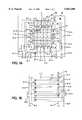
- FIG. 1(a)is a plan view illustrative of an LCD panel according to a first embodiment of the present invention
- FIG. 1(b)is a plan view of the panel shown in FIG. 1(a) except for a part of wirings;
- FIG. 2(a)is a plan view illustrative of an LCD panel according to a second embodiment of the present invention.
- FIG. 2(b)is a plan view of the panel shown in FIG. 2(a) except for a part of wirings;
- FIG. 3is a plan view illustrative of an LCD panel according to the prior art, schematically.
- an LCD panel 100is formed on a transparent insulating substrate 40 such as a glass substrate.
- This substrate 40has on a surface thereof an active matrix portion 50 surrounded by a broken line 51 and a shunt bus forming portion 60 around the matrix portion 50.
- the active matrix portion 50including a plurality of scan signal lines 1 arranged in rows, a plurality of data lines 3 arranged in columns, and a plurality of pixels 4 each connected to one of the scan signal lines 1 and one of the data lines 3, each of the pixels 4 being composed of a TFT, a pixel electrode and a storage capacitor, similarly to that shown in FIG. 3.
- the respective one ends of the storage capacitors of the pixels 4are connected in common to storage wiring 2.
- the shunt bus forming region 60includes four shunt buses 9-1 to 9-4 which are formed independently of one another in accordance with the present invention. Unlike the LCD panel shown in FIG. 3, the shunt buses 9-1 to 9-4 are grounded through respective resistors 8-1 to 8-3 and 8-5.
- the shunt bus 9-2is further connected to the odd-numbered scan signal lines 1-1, 1-3, . . . , and the shunt bus line 9-4 are connected to the even-numbered scan signal lines 1-2, 1-4, . . .
- the buses 9-2 and 9-4are provided respectively on the left and right sides of the active matrix portion 50.
- the shunt bus 9-1are connected the odd-numbered data lines 3-1, 3-3, . . .
- the shunt bus line 9-3are connected to the even-numbered data lines 3-2, 3-4, . . .
- These buses 9-1 and 9-3are provided respectively on the upper and lower sides of the active matrix portion 50.
- Pads 10-1 to 10-4are provided for the respective shunt buses 9-1 to 9-4.
- the resistors 8exists, the shunt buses 9 are grounded, and, therefore, the electrostatic charge, which may be occur during its manufacturing process, is discharged there-through. The TFT's are thereby protected against the electrostatic charge.
- the storage wiring 2 connected to the storage capacitors of the respective pixels 4is formed as a single wiring line in a meandering shape along the respective scan signal lines 1, as shown in FIG. 1(a).
- One end of the storage wiring 2is connected to a testing/measuring pad 12 and the other end is grounded through a resistor 8-4.
- discharge diodes 7are provided, as also shown in FIG. 1.
- test or check for a short-circuitis carried out as follows:
- a film of metal of such as Cris formed on a whole surface of the transparent insulating substrate 40 by a sputtering method.
- the metal film thus formedis selectively etched to form the scan signal lines 1, a part of the storage wiring 2-1, the shunt bus lines 9-2 and 9-4 and the resistors 8-2, 8-4 and 8-5, as shown in FIG. 1(b).
- the storage line 2consists of a plurality of horizontal segments 2-1 and a plurality of vertical segments 2-2.
- Each of the resistors 8-2, 8-4 and 8-5is formed of the same metal material as that of the shunt bus lines 9-2 and 9-4, but its width and length are made small and large, respectively, to provide a required resistance value. If desired, the resistors 8-2, 8-4 and 8-5 can have different values from each other.
- the respective segments 2-1 of the storage wiring 2are in floating condition.
- the short-circuit conditionis tested in this stage by contacting the probes between the pads 10-2 and 10-4. If any short-circuit is detected, it is understood that there is at least one residual metal layer connecting the adjacent wirings 1.
- the residual metal layeris, therefore, searched and then cut by using, for example, a laser. Repairing is thus performed.
- the wiringsare open electrically, it means that there is a portion of the wirings 1 or 2 in which it is physically cut. Therefore, it is also possible to repair it or reform.
- a gate insulating filmsuch as silicon oxide or a silicon nitride film is formed on the whole surface of the substrate and then a semiconductor film of such as amorphous silicon is selectively formed as channel regions of the TFT's. Further, through-holes are selectively formed in the gate insulating film. Thereafter, a film of metal such as Cr is again formed on the whole surface of the substrate and the data lines 3, the shunt bus lines 9-1 and 9-3 and the resistors 8-1 and 8-3 are selectively formed by selectively etching the metal film. In this case, the remaining segments 2-2 of the storage wiring 2 are formed as shown in FIG. 1(b) and connected to the portions 2-2 through the through-holes of the gate insulating film.
- the single meandering storage wiring 2is formed.
- Crossing portions 13 of the scan signal lines 1 and the storage wiring 2 and crossing points between the scan signal lines 1 and the data lines 3 shown in FIG. 1(a)are, of course, insulated by the insulating film.
- a portion of the scan signal line 1becomes as a gate electrode of the TFT and a portion of the data line 3 becomes a drain (source) of the TFT.
- the source (drain) electrodes of the TFT'sare formed simultaneously with the formation of the data lines 3.
- any short-circuit which may occur in a crossing point between wirings to be insulated from each otherby measuring a potential between the desired pads. Further, by measuring a potential between the pads 10-1 and 10-3, any short-circuit between two adjacent data lines 3 can be checked. If there is a short-circuit, it may be repaired depending upon a location thereof.
- pixel electrodesare formed by selectively providing transparent electrodes of material such as ITO, and, after covering the whole surface of the substrate by a protective insulating film, a panel assembling work is performed.
- the segments 2-1 of the storage wiring 2are in the floating state in the first step as mentioned previously. Therefore, the electro-static charge generated during the same step or during transportation of the substrate 40 to the subsequent step may destory the wiring segments 2-1.
- FIG. 2An LCD panel having a structure for further solving this problem is shown in FIG. 2 as a second embodiment of the present invention, in which the same constituents as those shown in FIG. 1 are depicted by the same reference numerals to omit further detailed description thereof.
- the whole storage line 2 and the associated resistor 8-4are formed simultaneously. Specifically, a film of metal such as Cr is formed on a whole surface of the transparent insulating substrate 40 and then selectively etched to form the scan signal lines 1, shunt buses 9-2 and 9-4 and resistors 8-2 and 8-5, etc. Simultaneously therewith, a meandering storage wiring 2, the grounding resistor 8-4 and the pad 12 are formed. With this construction, it is possible to prevent the storage wiring 2 from being damaged by the electrostatic charges. Further, since there is no crossing portion between the scan signal lines 1 and the storage wiring 2, there is no possibility of short-circuit between them.
- a shunt bus structurefor which a test for short-circuit between wirings can be performed easily while realizing a protection against damage due to electrostatic charge.
Landscapes
- Physics & Mathematics (AREA)
- Nonlinear Science (AREA)
- Engineering & Computer Science (AREA)
- Microelectronics & Electronic Packaging (AREA)
- Mathematical Physics (AREA)
- Chemical & Material Sciences (AREA)
- Crystallography & Structural Chemistry (AREA)
- General Physics & Mathematics (AREA)
- Optics & Photonics (AREA)
- Liquid Crystal (AREA)
Abstract
Description
Claims (12)
Applications Claiming Priority (2)
| Application Number | Priority Date | Filing Date | Title |
|---|---|---|---|
| JP6173694 | 1994-03-30 | ||
| JP6-061736 | 1994-03-30 |
Publications (1)
| Publication Number | Publication Date |
|---|---|
| US5852480Atrue US5852480A (en) | 1998-12-22 |
Family
ID=13179786
Family Applications (1)
| Application Number | Title | Priority Date | Filing Date |
|---|---|---|---|
| US08/411,273Expired - LifetimeUS5852480A (en) | 1994-03-30 | 1995-03-27 | LCD panel having a plurality of shunt buses |
Country Status (3)
| Country | Link |
|---|---|
| US (1) | US5852480A (en) |
| KR (1) | KR100192193B1 (en) |
| TW (1) | TW365425U (en) |
Cited By (39)
| Publication number | Priority date | Publication date | Assignee | Title |
|---|---|---|---|---|
| FR2758402A1 (en)* | 1997-01-10 | 1998-07-17 | Lg Electronics Inc | THIN LAYER TRANSISTOR MATRIX PRESENTING A CIRCUIT AGAINST STATIC ELECTRICITY |
| US5936687A (en)* | 1997-09-25 | 1999-08-10 | Samsung Electronics Co., Ltd. | Liquid crystal display having an electrostatic discharge protection circuit and a method for testing display quality using the circuit |
| US6043971A (en)* | 1998-11-04 | 2000-03-28 | L.G. Philips Lcd Co., Ltd. | Electrostatic discharge protection device for liquid crystal display using a COG package |
| US6049368A (en)* | 1997-09-12 | 2000-04-11 | Lg Lcd Inc. | Liquid crystal display having only one common line extending along the edge of substrate without connection pads |
| US6088073A (en)* | 1997-04-14 | 2000-07-11 | Casio Computer Co., Ltd. | Display device with destaticizing elements and an electrostatic pulse delaying element connected to each of the destaticizing elements |
| US6122030A (en)* | 1996-11-28 | 2000-09-19 | Sharp Kabushiki Kaisha | Insulating-film layer and sealant arrangement for protective circuit devices in a liquid crystal display device |
| US6184948B1 (en)* | 1997-02-11 | 2001-02-06 | Lg Electronics Inc. | Liquid crystal display device having a plurality of error detecting shorting bars and a method of manufacturing the same |
| US6288765B1 (en)* | 1998-10-01 | 2001-09-11 | Sharp Kabushiki Kaisha | Liquid crystal display device having improved thickness uniformity |
| US6304305B1 (en)* | 1997-10-20 | 2001-10-16 | Nec Corporation | Active matrix liquid crystal display |
| US6370965B1 (en)* | 1999-09-24 | 2002-04-16 | U.S. Philips Corporation | Capacitive sensing array devices |
| US20020044228A1 (en)* | 2000-10-11 | 2002-04-18 | Sang-Hun Oh | Array substrate for a liquid crystal display and method for fabricating thereof |
| US20020085169A1 (en)* | 2000-12-30 | 2002-07-04 | Choi Gyo Un | Liquid crystal display for testing defects of wiring in panel |
| US6570630B2 (en)* | 1997-03-26 | 2003-05-27 | Sharp Kabushiki Kaisha | Display panel |
| US20030133054A1 (en)* | 2002-01-04 | 2003-07-17 | Fujitsu Display Technologies Corporation | Substrate for display device and display device equipped therewith |
| US6636279B2 (en)* | 2000-07-24 | 2003-10-21 | International Business Machines Corporation | Display device and method of manufacturing the same |
| US20040169778A1 (en)* | 1998-06-29 | 2004-09-02 | Nobuyuki Suzuki | Liquid crystal display device |
| US20040232939A1 (en)* | 2003-05-20 | 2004-11-25 | Panelvision Technology, A California Corporation | Testing flat panel display plates using high frequency AC signals |
| KR100496283B1 (en)* | 2000-04-28 | 2005-06-17 | 삼성에스디아이 주식회사 | Plasma display panel |
| US20050162581A1 (en)* | 2003-12-18 | 2005-07-28 | Samsung Electronics Co., Ltd. | Thin film transistor array panel for a display |
| US20050180072A1 (en)* | 2004-02-16 | 2005-08-18 | Han-Chung Lai | Electrostatic discharge guide and liquid crystal display utilizing same |
| US20050225709A1 (en)* | 2001-09-28 | 2005-10-13 | Hitachi, Ltd. | Display device |
| EP1426914A4 (en)* | 2001-09-13 | 2005-11-23 | Seiko Epson Corp | ELECTRONIC DEVICE, METHOD FOR PRODUCING THE SAME, AND ELECTRONIC APPARATUS |
| US20060181500A1 (en)* | 2005-02-17 | 2006-08-17 | Seiko Epson Corporation | Electro-optical device, method of manufacturing electro-optical device, and electronic apparatus |
| US20070046316A1 (en)* | 2005-08-26 | 2007-03-01 | Guo-Feng Uei | Test circuit for flat panel display device |
| US20070097308A1 (en)* | 2005-10-31 | 2007-05-03 | Wen-Hsiung Liu | Thin film transistor array substrate and liquid crystal display |
| US20070109237A1 (en)* | 2005-11-14 | 2007-05-17 | Samsung Electronics Co., Ltd. | Display device |
| US20070109011A1 (en)* | 2005-11-15 | 2007-05-17 | Photon Dynamics, Inc. | Array Test Using The Shorting Bar And High Frequency Clock Signal For The Inspection Of TFT-LCD With Integrated Driver IC |
| US20090256153A1 (en)* | 1995-05-31 | 2009-10-15 | Sharp Kabushiki Kaisha | Thin film transistor matrix device and method for fabricating the same |
| US20100060815A1 (en)* | 2008-09-11 | 2010-03-11 | Hitachi Displays, Ltd. | Liquid crystal display device |
| CN1731205B (en)* | 2005-08-31 | 2010-06-09 | 友达光电股份有限公司 | Test circuit of flat display device |
| CN102981340A (en)* | 2012-12-11 | 2013-03-20 | 京东方科技集团股份有限公司 | Array substrate of liquid crystal display and manufacturing method |
| US20140185169A1 (en)* | 2012-12-28 | 2014-07-03 | Lg Display Co., Ltd. | Display device |
| US20160013264A1 (en)* | 2013-03-06 | 2016-01-14 | Seiko Epson Corporation | Electro-optical device, electronic apparatus, and drive circuit |
| US9267979B2 (en)* | 2013-12-31 | 2016-02-23 | Shenzhen China Star Optoelectronics Technology Co., Ltd | Line testing device for array substrate having dense number of wires and method for testing line of the array substrate having the dense number of wires |
| US20170269398A1 (en)* | 2016-03-21 | 2017-09-21 | Samsung Display Co., Ltd. | Display device and short circuit test method |
| US9966033B2 (en)* | 2016-04-13 | 2018-05-08 | Shenzhen China Star Optoelectronics Technology Co., Ltd. | Detection device for display panel |
| US10482837B2 (en)* | 2016-12-05 | 2019-11-19 | Mitsubishi Electric Corporation | Liquid crystal display and method of driving liquid crystal display |
| US11108028B2 (en) | 2017-04-25 | 2021-08-31 | Sumitomo Chemical Company, Limited | Manufacturing method for organic electronic device |
| US11121350B2 (en) | 2017-04-26 | 2021-09-14 | Sumitomo Chemical Company, Limited | Electrode-attached substrate, laminated substrate, and organic device manufacturing method |
Families Citing this family (1)
| Publication number | Priority date | Publication date | Assignee | Title |
|---|---|---|---|---|
| KR100467515B1 (en)* | 1997-10-07 | 2005-05-19 | 삼성전자주식회사 | Pattern generator for thin film transistor substrate test |
Citations (7)
| Publication number | Priority date | Publication date | Assignee | Title |
|---|---|---|---|---|
| JPS63106788A (en)* | 1986-10-24 | 1988-05-11 | 松下電器産業株式会社 | Manufacture of active matrix driven-type device |
| US5162901A (en)* | 1989-05-26 | 1992-11-10 | Sharp Kabushiki Kaisha | Active-matrix display device with added capacitance electrode wire and secondary wire connected thereto |
| US5235272A (en)* | 1991-06-17 | 1993-08-10 | Photon Dynamics, Inc. | Method and apparatus for automatically inspecting and repairing an active matrix LCD panel |
| US5373377A (en)* | 1992-02-21 | 1994-12-13 | Kabushiki Kaisha Toshiba | Liquid crystal device with shorting ring and transistors for electrostatic discharge protection |
| US5377030A (en)* | 1992-03-30 | 1994-12-27 | Sony Corporation | Method for testing active matrix liquid crystal by measuring voltage due to charge in a supplemental capacitor |
| US5504601A (en)* | 1992-07-15 | 1996-04-02 | Kabushiki Kaisha Toshiba | Liquid crystal dispaly apparatus with gap adjusting layers located between the display region and driver circuits |
| US5504348A (en)* | 1992-08-13 | 1996-04-02 | Casio Computer Co., Ltd. | Thin-film transistor array and liquid crystal display device using the thin-film transistor array |
- 1995
- 1995-03-27USUS08/411,273patent/US5852480A/ennot_activeExpired - Lifetime
- 1995-03-28TWTW086221301Upatent/TW365425U/enunknown
- 1995-03-30KRKR1019950007008Apatent/KR100192193B1/ennot_activeExpired - Lifetime
Patent Citations (7)
| Publication number | Priority date | Publication date | Assignee | Title |
|---|---|---|---|---|
| JPS63106788A (en)* | 1986-10-24 | 1988-05-11 | 松下電器産業株式会社 | Manufacture of active matrix driven-type device |
| US5162901A (en)* | 1989-05-26 | 1992-11-10 | Sharp Kabushiki Kaisha | Active-matrix display device with added capacitance electrode wire and secondary wire connected thereto |
| US5235272A (en)* | 1991-06-17 | 1993-08-10 | Photon Dynamics, Inc. | Method and apparatus for automatically inspecting and repairing an active matrix LCD panel |
| US5373377A (en)* | 1992-02-21 | 1994-12-13 | Kabushiki Kaisha Toshiba | Liquid crystal device with shorting ring and transistors for electrostatic discharge protection |
| US5377030A (en)* | 1992-03-30 | 1994-12-27 | Sony Corporation | Method for testing active matrix liquid crystal by measuring voltage due to charge in a supplemental capacitor |
| US5504601A (en)* | 1992-07-15 | 1996-04-02 | Kabushiki Kaisha Toshiba | Liquid crystal dispaly apparatus with gap adjusting layers located between the display region and driver circuits |
| US5504348A (en)* | 1992-08-13 | 1996-04-02 | Casio Computer Co., Ltd. | Thin-film transistor array and liquid crystal display device using the thin-film transistor array |
Cited By (88)
| Publication number | Priority date | Publication date | Assignee | Title |
|---|---|---|---|---|
| US8592816B2 (en)* | 1995-05-31 | 2013-11-26 | Sharp Kabushiki Kaisha | Thin film transistor matrix device including first and second connection lines |
| US20090256153A1 (en)* | 1995-05-31 | 2009-10-15 | Sharp Kabushiki Kaisha | Thin film transistor matrix device and method for fabricating the same |
| US20100117087A1 (en)* | 1995-05-31 | 2010-05-13 | Sharp Kabushiki Kaisha | Thin film transistor matrix device and method for fabricating the same |
| US20100214202A1 (en)* | 1995-05-31 | 2010-08-26 | Sharp Kabushiki Kaisha | Thin film transistor matrix device and method for fabricating the same |
| US7947983B2 (en) | 1995-05-31 | 2011-05-24 | Sharp Kabushiki Kaisha | Thin film transistor matrix device including first and second conducting connections formed outside an image display region |
| US7947982B2 (en) | 1995-05-31 | 2011-05-24 | Sharp Kabushiki Kaisha | Thin film transistor matrix device including a plurality of thin film transistors arranged on the substrate |
| US8258513B2 (en)* | 1995-05-31 | 2012-09-04 | Sharp Kabushiki Kaisha | Thin film transistor matrix device including first and second connection lines |
| US20130015451A1 (en)* | 1995-05-31 | 2013-01-17 | Sharp Kabushiki Kaisha | Thin film transistor matrix device and method for fabricating the same |
| US6122030A (en)* | 1996-11-28 | 2000-09-19 | Sharp Kabushiki Kaisha | Insulating-film layer and sealant arrangement for protective circuit devices in a liquid crystal display device |
| FR2758402A1 (en)* | 1997-01-10 | 1998-07-17 | Lg Electronics Inc | THIN LAYER TRANSISTOR MATRIX PRESENTING A CIRCUIT AGAINST STATIC ELECTRICITY |
| US6184948B1 (en)* | 1997-02-11 | 2001-02-06 | Lg Electronics Inc. | Liquid crystal display device having a plurality of error detecting shorting bars and a method of manufacturing the same |
| US6765630B2 (en) | 1997-03-26 | 2004-07-20 | Sharp Kabushiki Kaisha | Display panel |
| US6570630B2 (en)* | 1997-03-26 | 2003-05-27 | Sharp Kabushiki Kaisha | Display panel |
| US20030112402A1 (en)* | 1997-03-26 | 2003-06-19 | Sharp Kabushiki Kaisha | Display panel |
| US20030117537A1 (en)* | 1997-03-26 | 2003-06-26 | Sharp Kabushiki Kaisha | Display panel |
| US6088073A (en)* | 1997-04-14 | 2000-07-11 | Casio Computer Co., Ltd. | Display device with destaticizing elements and an electrostatic pulse delaying element connected to each of the destaticizing elements |
| US6049368A (en)* | 1997-09-12 | 2000-04-11 | Lg Lcd Inc. | Liquid crystal display having only one common line extending along the edge of substrate without connection pads |
| US6252643B1 (en)* | 1997-09-12 | 2001-06-26 | Lg Lcd Inc. | Liquid crystal display having only one common line extending along substrate edge |
| US5936687A (en)* | 1997-09-25 | 1999-08-10 | Samsung Electronics Co., Ltd. | Liquid crystal display having an electrostatic discharge protection circuit and a method for testing display quality using the circuit |
| US6304305B1 (en)* | 1997-10-20 | 2001-10-16 | Nec Corporation | Active matrix liquid crystal display |
| US20050185106A1 (en)* | 1998-06-29 | 2005-08-25 | Nobuyuki Suzuki | Liquid crystal display device |
| US20040169778A1 (en)* | 1998-06-29 | 2004-09-02 | Nobuyuki Suzuki | Liquid crystal display device |
| US6888584B2 (en)* | 1998-06-29 | 2005-05-03 | Hitachi, Ltd. | Liquid crystal display device |
| US7129999B2 (en) | 1998-06-29 | 2006-10-31 | Hitachi, Ltd. | Liquid crystal display device |
| US6288765B1 (en)* | 1998-10-01 | 2001-09-11 | Sharp Kabushiki Kaisha | Liquid crystal display device having improved thickness uniformity |
| US6043971A (en)* | 1998-11-04 | 2000-03-28 | L.G. Philips Lcd Co., Ltd. | Electrostatic discharge protection device for liquid crystal display using a COG package |
| US6370965B1 (en)* | 1999-09-24 | 2002-04-16 | U.S. Philips Corporation | Capacitive sensing array devices |
| KR100496283B1 (en)* | 2000-04-28 | 2005-06-17 | 삼성에스디아이 주식회사 | Plasma display panel |
| US6636279B2 (en)* | 2000-07-24 | 2003-10-21 | International Business Machines Corporation | Display device and method of manufacturing the same |
| US6930732B2 (en)* | 2000-10-11 | 2005-08-16 | Lg.Philips Lcd Co., Ltd. | Array substrate for a liquid crystal display |
| US6924179B2 (en) | 2000-10-11 | 2005-08-02 | Lg.Philips Lcd Co., Ltd. | Array substrate for a liquid crystal display and method for fabricating thereof |
| US20040149990A1 (en)* | 2000-10-11 | 2004-08-05 | Sung-Hun Oh | Array substrate for a liquid crystal display and method for fabricating thereof |
| US20020044228A1 (en)* | 2000-10-11 | 2002-04-18 | Sang-Hun Oh | Array substrate for a liquid crystal display and method for fabricating thereof |
| US6999153B2 (en)* | 2000-12-30 | 2006-02-14 | Boe-Hydis Technology Co., Ltd. | Liquid crystal display for testing defects of wiring in panel |
| US20020085169A1 (en)* | 2000-12-30 | 2002-07-04 | Choi Gyo Un | Liquid crystal display for testing defects of wiring in panel |
| EP1426914A4 (en)* | 2001-09-13 | 2005-11-23 | Seiko Epson Corp | ELECTRONIC DEVICE, METHOD FOR PRODUCING THE SAME, AND ELECTRONIC APPARATUS |
| US20090079889A1 (en)* | 2001-09-28 | 2009-03-26 | Hitachi, Ltd. | Display device |
| US7002658B2 (en) | 2001-09-28 | 2006-02-21 | Hitachi, Ltd. | Display device |
| US7821584B2 (en) | 2001-09-28 | 2010-10-26 | Hitachi, Ltd. | Display device |
| US7164453B2 (en) | 2001-09-28 | 2007-01-16 | Hitachi, Ltd. | Display device |
| US20050225709A1 (en)* | 2001-09-28 | 2005-10-13 | Hitachi, Ltd. | Display device |
| US20060152642A1 (en)* | 2001-09-28 | 2006-07-13 | Hitachi, Ltd. | Display device |
| US20050231678A1 (en)* | 2001-09-28 | 2005-10-20 | Hitachi, Ltd. | Display device |
| US7471349B2 (en) | 2001-09-28 | 2008-12-30 | Hitachi, Ltd. | Display device |
| US20060187370A1 (en)* | 2002-01-04 | 2006-08-24 | Atuyuki Hoshino | Substrate for display device and display device equipped therewith |
| US7061553B2 (en)* | 2002-01-04 | 2006-06-13 | Sharp Kabushiki Kaisha | Substrate for display device and display device equipped therewith |
| US20030133054A1 (en)* | 2002-01-04 | 2003-07-17 | Fujitsu Display Technologies Corporation | Substrate for display device and display device equipped therewith |
| US7626646B2 (en) | 2002-01-04 | 2009-12-01 | Sharp Kabushiki Kaisha | Substrate for display device and display device equipped therewith |
| US20060061380A1 (en)* | 2003-05-20 | 2006-03-23 | Panelvision Technology, A California Corporation | Testing flat panel display plates using high frequency AC signals |
| US20040232939A1 (en)* | 2003-05-20 | 2004-11-25 | Panelvision Technology, A California Corporation | Testing flat panel display plates using high frequency AC signals |
| US6987400B2 (en) | 2003-05-20 | 2006-01-17 | Panelvision Technologies | Testing flat panel display plates using high frequency AC signals |
| US7297979B2 (en)* | 2003-12-18 | 2007-11-20 | Samsung Electronics Co., Ltd. | Thin film transistor array panel for a display |
| US20080029784A1 (en)* | 2003-12-18 | 2008-02-07 | Do-Gi Lim | Thin film transistor array panel for a display |
| CN100444006C (en)* | 2003-12-18 | 2008-12-17 | 三星电子株式会社 | Thin film transistor array panel for display |
| US7746417B2 (en) | 2003-12-18 | 2010-06-29 | Samsung Electronics Co., Ltd. | Thin film transistor array panel for a display |
| US20050162581A1 (en)* | 2003-12-18 | 2005-07-28 | Samsung Electronics Co., Ltd. | Thin film transistor array panel for a display |
| US20050180072A1 (en)* | 2004-02-16 | 2005-08-18 | Han-Chung Lai | Electrostatic discharge guide and liquid crystal display utilizing same |
| US20080024947A1 (en)* | 2004-02-16 | 2008-01-31 | Au Optronics Corp. | Electrostatic discharge guide and liquid crystal display utilizing same |
| US7474516B2 (en) | 2004-02-16 | 2009-01-06 | Au Optronics Corp. | Electrostatic discharge guide and liquid crystal display utilizing same |
| US7317602B2 (en)* | 2004-02-16 | 2008-01-08 | Au Optronics Corp. | Electrostatic discharge guide and liquid crystal display utilizing same |
| US20060181500A1 (en)* | 2005-02-17 | 2006-08-17 | Seiko Epson Corporation | Electro-optical device, method of manufacturing electro-optical device, and electronic apparatus |
| US7903186B2 (en)* | 2005-02-17 | 2011-03-08 | Seiko Epson Corporation | Electro-optical device, method of manufacturing electro-optical device, and electronic apparatus |
| US20070046316A1 (en)* | 2005-08-26 | 2007-03-01 | Guo-Feng Uei | Test circuit for flat panel display device |
| US7336093B2 (en) | 2005-08-26 | 2008-02-26 | Au Optronics Corporation | Test circuit for flat panel display device |
| CN1731205B (en)* | 2005-08-31 | 2010-06-09 | 友达光电股份有限公司 | Test circuit of flat display device |
| US20070097308A1 (en)* | 2005-10-31 | 2007-05-03 | Wen-Hsiung Liu | Thin film transistor array substrate and liquid crystal display |
| TWI402795B (en)* | 2005-11-14 | 2013-07-21 | Samsung Display Co Ltd | Display device |
| US20070109237A1 (en)* | 2005-11-14 | 2007-05-17 | Samsung Electronics Co., Ltd. | Display device |
| US8411001B2 (en)* | 2005-11-14 | 2013-04-02 | Samsung Display Co., Ltd. | Display device with floating bar |
| WO2007059315A3 (en)* | 2005-11-15 | 2008-01-10 | Photon Dynamics Inc | Array test using the shorting bar and high frequency clock signal for the inspection of tft-lcd with integrated driver ic |
| US7714589B2 (en)* | 2005-11-15 | 2010-05-11 | Photon Dynamics, Inc. | Array test using the shorting bar and high frequency clock signal for the inspection of TFT-LCD with integrated driver IC |
| US20070109011A1 (en)* | 2005-11-15 | 2007-05-17 | Photon Dynamics, Inc. | Array Test Using The Shorting Bar And High Frequency Clock Signal For The Inspection Of TFT-LCD With Integrated Driver IC |
| US20100060815A1 (en)* | 2008-09-11 | 2010-03-11 | Hitachi Displays, Ltd. | Liquid crystal display device |
| TWI402587B (en)* | 2008-09-11 | 2013-07-21 | Hitachi Displays Ltd | Liquid crystal display device |
| CN102981340B (en)* | 2012-12-11 | 2015-11-25 | 京东方科技集团股份有限公司 | A kind of array base palte of liquid crystal display and manufacture method |
| CN102981340A (en)* | 2012-12-11 | 2013-03-20 | 京东方科技集团股份有限公司 | Array substrate of liquid crystal display and manufacturing method |
| US9153192B2 (en)* | 2012-12-28 | 2015-10-06 | Lg Display Co., Ltd | Display device |
| US20140185169A1 (en)* | 2012-12-28 | 2014-07-03 | Lg Display Co., Ltd. | Display device |
| US20160013264A1 (en)* | 2013-03-06 | 2016-01-14 | Seiko Epson Corporation | Electro-optical device, electronic apparatus, and drive circuit |
| US9267979B2 (en)* | 2013-12-31 | 2016-02-23 | Shenzhen China Star Optoelectronics Technology Co., Ltd | Line testing device for array substrate having dense number of wires and method for testing line of the array substrate having the dense number of wires |
| US10444554B2 (en)* | 2016-03-21 | 2019-10-15 | Samsung Display Co., Ltd. | Display device and short circuit test method |
| US20170269398A1 (en)* | 2016-03-21 | 2017-09-21 | Samsung Display Co., Ltd. | Display device and short circuit test method |
| US10018858B2 (en)* | 2016-03-21 | 2018-07-10 | Samsung Display Co., Ltd. | Display device and short circuit test method |
| US9966033B2 (en)* | 2016-04-13 | 2018-05-08 | Shenzhen China Star Optoelectronics Technology Co., Ltd. | Detection device for display panel |
| US10482837B2 (en)* | 2016-12-05 | 2019-11-19 | Mitsubishi Electric Corporation | Liquid crystal display and method of driving liquid crystal display |
| US10643564B2 (en) | 2016-12-05 | 2020-05-05 | Mitsubishi Electric Corporation | Liquid crystal display and method of driving liquid crystal display |
| US11108028B2 (en) | 2017-04-25 | 2021-08-31 | Sumitomo Chemical Company, Limited | Manufacturing method for organic electronic device |
| US11121350B2 (en) | 2017-04-26 | 2021-09-14 | Sumitomo Chemical Company, Limited | Electrode-attached substrate, laminated substrate, and organic device manufacturing method |
Also Published As
| Publication number | Publication date |
|---|---|
| TW365425U (en) | 1999-07-21 |
| KR100192193B1 (en) | 1999-06-15 |
Similar Documents
| Publication | Publication Date | Title |
|---|---|---|
| US5852480A (en) | LCD panel having a plurality of shunt buses | |
| US7139044B2 (en) | Thin film transistor array panel | |
| JP3029531B2 (en) | Liquid crystal display | |
| EP0842536B1 (en) | Semiconductor switch array with electrostatic discharge protection and method of fabricating | |
| JP2715936B2 (en) | Thin film transistor type liquid crystal display device and manufacturing method thereof | |
| US8072034B2 (en) | Array substrate and method of manufacturing the same | |
| US7888680B2 (en) | Semiconductor device | |
| US20130294003A1 (en) | Substrate for display and liquid crystal display utilizing the same | |
| EP0369828A2 (en) | Active matrix liquid crystal display panel with an electrostatic protection circuit | |
| JP5613291B2 (en) | Substrate for liquid crystal display device, liquid crystal display device and method for manufacturing the same | |
| JP3006584B2 (en) | Thin film transistor array | |
| JP4516638B2 (en) | Substrate for liquid crystal display device, liquid crystal display device and method for manufacturing the same | |
| JP2713211B2 (en) | LCD panel | |
| KR100490040B1 (en) | Liquid crystal display device with two or more shorting bars and method for manufacturing same | |
| KR100576629B1 (en) | TFT array board of liquid crystal display and inspection method | |
| KR100299686B1 (en) | Liquid crystal display device having static electricity preventing function and manufacturing method thereof | |
| JP3162526B2 (en) | Method for manufacturing active matrix type liquid crystal display element | |
| JPH11150275A (en) | Thin film transistor array substrate | |
| KR19990066081A (en) | Wiring structure including electrostatic protection element and method for manufacturing same | |
| KR100670057B1 (en) | Thin film transistor substrate for liquid crystal display |
Legal Events
| Date | Code | Title | Description |
|---|---|---|---|
| AS | Assignment | Owner name:NEC CORPORATION Free format text:ASSIGNMENT OF ASSIGNORS INTEREST;ASSIGNORS:YAJIMA, AKIHIRO;NAKASHIMA, KOHJI;REEL/FRAME:007416/0269 Effective date:19950322 | |
| STCF | Information on status: patent grant | Free format text:PATENTED CASE | |
| FPAY | Fee payment | Year of fee payment:4 | |
| AS | Assignment | Owner name:NEC LCD TECHNOLOGIES, LTD., JAPAN Free format text:ASSIGNMENT OF ASSIGNORS INTEREST;ASSIGNOR:NEC CORPORATION;REEL/FRAME:014108/0248 Effective date:20030401 | |
| FPAY | Fee payment | Year of fee payment:8 | |
| FPAY | Fee payment | Year of fee payment:12 | |
| AS | Assignment | Owner name:NEC CORPORATION,JAPAN Free format text:ASSIGNMENT OF ASSIGNORS INTEREST;ASSIGNOR:NEC LCD TECHNOLOGIES, LTD.;REEL/FRAME:024492/0176 Effective date:20100301 Owner name:NEC CORPORATION, JAPAN Free format text:ASSIGNMENT OF ASSIGNORS INTEREST;ASSIGNOR:NEC LCD TECHNOLOGIES, LTD.;REEL/FRAME:024492/0176 Effective date:20100301 | |
| FEPP | Fee payment procedure | Free format text:PAYOR NUMBER ASSIGNED (ORIGINAL EVENT CODE: ASPN); ENTITY STATUS OF PATENT OWNER: LARGE ENTITY | |
| AS | Assignment | Owner name:GETNER FOUNDATION LLC, DELAWARE Free format text:ASSIGNMENT OF ASSIGNORS INTEREST;ASSIGNOR:NEC CORPORATION;REEL/FRAME:026254/0381 Effective date:20110418 | |
| AS | Assignment | Owner name:VISTA PEAK VENTURES, LLC, TEXAS Free format text:ASSIGNMENT OF ASSIGNORS INTEREST;ASSIGNOR:GETNER FOUNDATION LLC;REEL/FRAME:045469/0164 Effective date:20180213 |