US5847781A - Liquid crystal display device comprises a light-blocking layer and a plurality of data lines which have a width that is larger than the width of a semiconductor layer - Google Patents
Liquid crystal display device comprises a light-blocking layer and a plurality of data lines which have a width that is larger than the width of a semiconductor layerDownload PDFInfo
- Publication number
- US5847781A US5847781AUS08/683,408US68340896AUS5847781AUS 5847781 AUS5847781 AUS 5847781AUS 68340896 AUS68340896 AUS 68340896AUS 5847781 AUS5847781 AUS 5847781A
- Authority
- US
- United States
- Prior art keywords
- data lines
- pixel electrodes
- insulating film
- scanning signal
- semiconductor layer
- Prior art date
- Legal status (The legal status is an assumption and is not a legal conclusion. Google has not performed a legal analysis and makes no representation as to the accuracy of the status listed.)
- Expired - Lifetime
Links
Images


Classifications
- G—PHYSICS
- G02—OPTICS
- G02F—OPTICAL DEVICES OR ARRANGEMENTS FOR THE CONTROL OF LIGHT BY MODIFICATION OF THE OPTICAL PROPERTIES OF THE MEDIA OF THE ELEMENTS INVOLVED THEREIN; NON-LINEAR OPTICS; FREQUENCY-CHANGING OF LIGHT; OPTICAL LOGIC ELEMENTS; OPTICAL ANALOGUE/DIGITAL CONVERTERS
- G02F1/00—Devices or arrangements for the control of the intensity, colour, phase, polarisation or direction of light arriving from an independent light source, e.g. switching, gating or modulating; Non-linear optics
- G02F1/01—Devices or arrangements for the control of the intensity, colour, phase, polarisation or direction of light arriving from an independent light source, e.g. switching, gating or modulating; Non-linear optics for the control of the intensity, phase, polarisation or colour
- G02F1/13—Devices or arrangements for the control of the intensity, colour, phase, polarisation or direction of light arriving from an independent light source, e.g. switching, gating or modulating; Non-linear optics for the control of the intensity, phase, polarisation or colour based on liquid crystals, e.g. single liquid crystal display cells
- G02F1/133—Constructional arrangements; Operation of liquid crystal cells; Circuit arrangements
- G02F1/136—Liquid crystal cells structurally associated with a semi-conducting layer or substrate, e.g. cells forming part of an integrated circuit
- G—PHYSICS
- G02—OPTICS
- G02F—OPTICAL DEVICES OR ARRANGEMENTS FOR THE CONTROL OF LIGHT BY MODIFICATION OF THE OPTICAL PROPERTIES OF THE MEDIA OF THE ELEMENTS INVOLVED THEREIN; NON-LINEAR OPTICS; FREQUENCY-CHANGING OF LIGHT; OPTICAL LOGIC ELEMENTS; OPTICAL ANALOGUE/DIGITAL CONVERTERS
- G02F1/00—Devices or arrangements for the control of the intensity, colour, phase, polarisation or direction of light arriving from an independent light source, e.g. switching, gating or modulating; Non-linear optics
- G02F1/01—Devices or arrangements for the control of the intensity, colour, phase, polarisation or direction of light arriving from an independent light source, e.g. switching, gating or modulating; Non-linear optics for the control of the intensity, phase, polarisation or colour
- G02F1/13—Devices or arrangements for the control of the intensity, colour, phase, polarisation or direction of light arriving from an independent light source, e.g. switching, gating or modulating; Non-linear optics for the control of the intensity, phase, polarisation or colour based on liquid crystals, e.g. single liquid crystal display cells
- G02F1/133—Constructional arrangements; Operation of liquid crystal cells; Circuit arrangements
- G02F1/1333—Constructional arrangements; Manufacturing methods
- G02F1/1345—Conductors connecting electrodes to cell terminals
- G02F1/13458—Terminal pads
- G—PHYSICS
- G02—OPTICS
- G02F—OPTICAL DEVICES OR ARRANGEMENTS FOR THE CONTROL OF LIGHT BY MODIFICATION OF THE OPTICAL PROPERTIES OF THE MEDIA OF THE ELEMENTS INVOLVED THEREIN; NON-LINEAR OPTICS; FREQUENCY-CHANGING OF LIGHT; OPTICAL LOGIC ELEMENTS; OPTICAL ANALOGUE/DIGITAL CONVERTERS
- G02F1/00—Devices or arrangements for the control of the intensity, colour, phase, polarisation or direction of light arriving from an independent light source, e.g. switching, gating or modulating; Non-linear optics
- G02F1/01—Devices or arrangements for the control of the intensity, colour, phase, polarisation or direction of light arriving from an independent light source, e.g. switching, gating or modulating; Non-linear optics for the control of the intensity, phase, polarisation or colour
- G02F1/13—Devices or arrangements for the control of the intensity, colour, phase, polarisation or direction of light arriving from an independent light source, e.g. switching, gating or modulating; Non-linear optics for the control of the intensity, phase, polarisation or colour based on liquid crystals, e.g. single liquid crystal display cells
- G02F1/133—Constructional arrangements; Operation of liquid crystal cells; Circuit arrangements
- G02F1/1333—Constructional arrangements; Manufacturing methods
- G02F1/1343—Electrodes
- G—PHYSICS
- G02—OPTICS
- G02F—OPTICAL DEVICES OR ARRANGEMENTS FOR THE CONTROL OF LIGHT BY MODIFICATION OF THE OPTICAL PROPERTIES OF THE MEDIA OF THE ELEMENTS INVOLVED THEREIN; NON-LINEAR OPTICS; FREQUENCY-CHANGING OF LIGHT; OPTICAL LOGIC ELEMENTS; OPTICAL ANALOGUE/DIGITAL CONVERTERS
- G02F1/00—Devices or arrangements for the control of the intensity, colour, phase, polarisation or direction of light arriving from an independent light source, e.g. switching, gating or modulating; Non-linear optics
- G02F1/01—Devices or arrangements for the control of the intensity, colour, phase, polarisation or direction of light arriving from an independent light source, e.g. switching, gating or modulating; Non-linear optics for the control of the intensity, phase, polarisation or colour
- G02F1/13—Devices or arrangements for the control of the intensity, colour, phase, polarisation or direction of light arriving from an independent light source, e.g. switching, gating or modulating; Non-linear optics for the control of the intensity, phase, polarisation or colour based on liquid crystals, e.g. single liquid crystal display cells
- G02F1/133—Constructional arrangements; Operation of liquid crystal cells; Circuit arrangements
- G02F1/136—Liquid crystal cells structurally associated with a semi-conducting layer or substrate, e.g. cells forming part of an integrated circuit
- G02F1/1362—Active matrix addressed cells
- G02F1/136209—Light shielding layers, e.g. black matrix, incorporated in the active matrix substrate, e.g. structurally associated with the switching element
- G—PHYSICS
- G02—OPTICS
- G02F—OPTICAL DEVICES OR ARRANGEMENTS FOR THE CONTROL OF LIGHT BY MODIFICATION OF THE OPTICAL PROPERTIES OF THE MEDIA OF THE ELEMENTS INVOLVED THEREIN; NON-LINEAR OPTICS; FREQUENCY-CHANGING OF LIGHT; OPTICAL LOGIC ELEMENTS; OPTICAL ANALOGUE/DIGITAL CONVERTERS
- G02F1/00—Devices or arrangements for the control of the intensity, colour, phase, polarisation or direction of light arriving from an independent light source, e.g. switching, gating or modulating; Non-linear optics
- G02F1/01—Devices or arrangements for the control of the intensity, colour, phase, polarisation or direction of light arriving from an independent light source, e.g. switching, gating or modulating; Non-linear optics for the control of the intensity, phase, polarisation or colour
- G02F1/13—Devices or arrangements for the control of the intensity, colour, phase, polarisation or direction of light arriving from an independent light source, e.g. switching, gating or modulating; Non-linear optics for the control of the intensity, phase, polarisation or colour based on liquid crystals, e.g. single liquid crystal display cells
- G02F1/133—Constructional arrangements; Operation of liquid crystal cells; Circuit arrangements
- G02F1/136—Liquid crystal cells structurally associated with a semi-conducting layer or substrate, e.g. cells forming part of an integrated circuit
- G02F1/1362—Active matrix addressed cells
- G02F1/136227—Through-hole connection of the pixel electrode to the active element through an insulation layer
- G—PHYSICS
- G02—OPTICS
- G02F—OPTICAL DEVICES OR ARRANGEMENTS FOR THE CONTROL OF LIGHT BY MODIFICATION OF THE OPTICAL PROPERTIES OF THE MEDIA OF THE ELEMENTS INVOLVED THEREIN; NON-LINEAR OPTICS; FREQUENCY-CHANGING OF LIGHT; OPTICAL LOGIC ELEMENTS; OPTICAL ANALOGUE/DIGITAL CONVERTERS
- G02F1/00—Devices or arrangements for the control of the intensity, colour, phase, polarisation or direction of light arriving from an independent light source, e.g. switching, gating or modulating; Non-linear optics
- G02F1/01—Devices or arrangements for the control of the intensity, colour, phase, polarisation or direction of light arriving from an independent light source, e.g. switching, gating or modulating; Non-linear optics for the control of the intensity, phase, polarisation or colour
- G02F1/13—Devices or arrangements for the control of the intensity, colour, phase, polarisation or direction of light arriving from an independent light source, e.g. switching, gating or modulating; Non-linear optics for the control of the intensity, phase, polarisation or colour based on liquid crystals, e.g. single liquid crystal display cells
- G02F1/133—Constructional arrangements; Operation of liquid crystal cells; Circuit arrangements
- G02F1/136—Liquid crystal cells structurally associated with a semi-conducting layer or substrate, e.g. cells forming part of an integrated circuit
- G02F1/1362—Active matrix addressed cells
- G02F1/136286—Wiring, e.g. gate line, drain line
- H—ELECTRICITY
- H10—SEMICONDUCTOR DEVICES; ELECTRIC SOLID-STATE DEVICES NOT OTHERWISE PROVIDED FOR
- H10D—INORGANIC ELECTRIC SEMICONDUCTOR DEVICES
- H10D30/00—Field-effect transistors [FET]
- H10D30/60—Insulated-gate field-effect transistors [IGFET]
- H10D30/67—Thin-film transistors [TFT]
- H10D30/6704—Thin-film transistors [TFT] having supplementary regions or layers in the thin films or in the insulated bulk substrates for controlling properties of the device
- H10D30/6713—Thin-film transistors [TFT] having supplementary regions or layers in the thin films or in the insulated bulk substrates for controlling properties of the device characterised by the properties of the source or drain regions, e.g. compositions or sectional shapes
- H—ELECTRICITY
- H10—SEMICONDUCTOR DEVICES; ELECTRIC SOLID-STATE DEVICES NOT OTHERWISE PROVIDED FOR
- H10D—INORGANIC ELECTRIC SEMICONDUCTOR DEVICES
- H10D30/00—Field-effect transistors [FET]
- H10D30/60—Insulated-gate field-effect transistors [IGFET]
- H10D30/67—Thin-film transistors [TFT]
- H10D30/6729—Thin-film transistors [TFT] characterised by the electrodes
- H10D30/673—Thin-film transistors [TFT] characterised by the electrodes characterised by the shapes, relative sizes or dispositions of the gate electrodes
- H10D30/6732—Bottom-gate only TFTs
- H—ELECTRICITY
- H10—SEMICONDUCTOR DEVICES; ELECTRIC SOLID-STATE DEVICES NOT OTHERWISE PROVIDED FOR
- H10D—INORGANIC ELECTRIC SEMICONDUCTOR DEVICES
- H10D30/00—Field-effect transistors [FET]
- H10D30/60—Insulated-gate field-effect transistors [IGFET]
- H10D30/67—Thin-film transistors [TFT]
- H10D30/674—Thin-film transistors [TFT] characterised by the active materials
- H10D30/6741—Group IV materials, e.g. germanium or silicon carbide
- H10D30/6743—Silicon
- H10D30/6746—Amorphous silicon
- H—ELECTRICITY
- H10—SEMICONDUCTOR DEVICES; ELECTRIC SOLID-STATE DEVICES NOT OTHERWISE PROVIDED FOR
- H10D—INORGANIC ELECTRIC SEMICONDUCTOR DEVICES
- H10D86/00—Integrated devices formed in or on insulating or conducting substrates, e.g. formed in silicon-on-insulator [SOI] substrates or on stainless steel or glass substrates
- H10D86/40—Integrated devices formed in or on insulating or conducting substrates, e.g. formed in silicon-on-insulator [SOI] substrates or on stainless steel or glass substrates characterised by multiple TFTs
- H10D86/441—Interconnections, e.g. scanning lines
- H—ELECTRICITY
- H10—SEMICONDUCTOR DEVICES; ELECTRIC SOLID-STATE DEVICES NOT OTHERWISE PROVIDED FOR
- H10D—INORGANIC ELECTRIC SEMICONDUCTOR DEVICES
- H10D86/00—Integrated devices formed in or on insulating or conducting substrates, e.g. formed in silicon-on-insulator [SOI] substrates or on stainless steel or glass substrates
- H10D86/40—Integrated devices formed in or on insulating or conducting substrates, e.g. formed in silicon-on-insulator [SOI] substrates or on stainless steel or glass substrates characterised by multiple TFTs
- H10D86/60—Integrated devices formed in or on insulating or conducting substrates, e.g. formed in silicon-on-insulator [SOI] substrates or on stainless steel or glass substrates characterised by multiple TFTs wherein the TFTs are in active matrices
- G—PHYSICS
- G02—OPTICS
- G02F—OPTICAL DEVICES OR ARRANGEMENTS FOR THE CONTROL OF LIGHT BY MODIFICATION OF THE OPTICAL PROPERTIES OF THE MEDIA OF THE ELEMENTS INVOLVED THEREIN; NON-LINEAR OPTICS; FREQUENCY-CHANGING OF LIGHT; OPTICAL LOGIC ELEMENTS; OPTICAL ANALOGUE/DIGITAL CONVERTERS
- G02F1/00—Devices or arrangements for the control of the intensity, colour, phase, polarisation or direction of light arriving from an independent light source, e.g. switching, gating or modulating; Non-linear optics
- G02F1/01—Devices or arrangements for the control of the intensity, colour, phase, polarisation or direction of light arriving from an independent light source, e.g. switching, gating or modulating; Non-linear optics for the control of the intensity, phase, polarisation or colour
- G02F1/13—Devices or arrangements for the control of the intensity, colour, phase, polarisation or direction of light arriving from an independent light source, e.g. switching, gating or modulating; Non-linear optics for the control of the intensity, phase, polarisation or colour based on liquid crystals, e.g. single liquid crystal display cells
- G02F1/133—Constructional arrangements; Operation of liquid crystal cells; Circuit arrangements
- G02F1/1333—Constructional arrangements; Manufacturing methods
- G02F1/1345—Conductors connecting electrodes to cell terminals
- G02F1/13452—Conductors connecting driver circuitry and terminals of panels
- G—PHYSICS
- G02—OPTICS
- G02F—OPTICAL DEVICES OR ARRANGEMENTS FOR THE CONTROL OF LIGHT BY MODIFICATION OF THE OPTICAL PROPERTIES OF THE MEDIA OF THE ELEMENTS INVOLVED THEREIN; NON-LINEAR OPTICS; FREQUENCY-CHANGING OF LIGHT; OPTICAL LOGIC ELEMENTS; OPTICAL ANALOGUE/DIGITAL CONVERTERS
- G02F1/00—Devices or arrangements for the control of the intensity, colour, phase, polarisation or direction of light arriving from an independent light source, e.g. switching, gating or modulating; Non-linear optics
- G02F1/01—Devices or arrangements for the control of the intensity, colour, phase, polarisation or direction of light arriving from an independent light source, e.g. switching, gating or modulating; Non-linear optics for the control of the intensity, phase, polarisation or colour
- G02F1/13—Devices or arrangements for the control of the intensity, colour, phase, polarisation or direction of light arriving from an independent light source, e.g. switching, gating or modulating; Non-linear optics for the control of the intensity, phase, polarisation or colour based on liquid crystals, e.g. single liquid crystal display cells
- G02F1/133—Constructional arrangements; Operation of liquid crystal cells; Circuit arrangements
- G02F1/136—Liquid crystal cells structurally associated with a semi-conducting layer or substrate, e.g. cells forming part of an integrated circuit
- G02F1/1362—Active matrix addressed cells
- G02F1/136218—Shield electrodes
Definitions
- the present inventionrelates to an active matrix addressing type liquid crystal display device using thin film transistors (TFTs) and a method of manufacturing the same.
- TFTsthin film transistors
- An active matrix addressing type liquid crystal display deviceincludes switching elements each being provided correspondingly to one of a plurality of pixel electrodes arranged in a matrix.
- the active matrix addressing type displayhas a feature that liquid crystal at each pixel is theoretically driven at all times and accordingly it is higher in contrast than a simple matrix type adopting time-multiplexed driving.
- Such an active matrix addressing type displayhas become essential, particularly for color display.
- a TFT arrangement used for a conventional active matrix addressing type liquid crystal display deviceincludes a scanning signal line (gate line) formed on a transparent insulating substrate; a gate insulator formed on the scanning signal line; a semiconductor layer formed on the gate insulator; and a drain electrode (data line) and a source electrode formed on the semiconductor film, wherein the source electrode is connected to a transparent pixel electrode and the drain electrode (data line) is supplied with a video signal voltage.
- a TFT structure of a type in which a gate electrode is formed directly on a substrateis generally called an inverted staggered structure. Such a TFT is known from Japanese Patent Laid-open No. Sho 61-161764.
- the liquid crystal display device using TFTsenables active addressing and thereby it exhibits high contrast; however, it is complicated in formation of TFTs on a substrate and also requires six or more photolithography steps. This is disadvantageous in terms of increasing a manufacturing cost of a TFT substrate and decreasing a processing yield with the increased number of manufacturing steps due to dust or dirt.
- a method for simplifying manufacturing stepshas been proposed, wherein a gate insulator, a semiconductor layer, and a metal film (for drain and source electrodes) are formed; the semiconductor layer is processed using the metal film as a mask; and a transparent electrode is formed.
- This prior artis disadvantageous in that in the case where the metal film forming the source electrode is smaller in etching rate than the semiconductor film, the source electrode overhangs and increases open line defect probabilities for the transparent electrode due to the presence of a step at the overhang. In other words, in the above prior art the manufacturing yield has never been considered sufficiently.
- An object of the present inventionis to provide an active matrix addressing type liquid crystal display device capable of obtaining a display screen of high contrast and low cross talk.
- Another object of the present inventionis to provide a method of making an active matrix addressing type liquid crystal display device, which is capable of reducing the number of manufacturing steps and increasing a manufacturing yield.
- a liquid crystal display deviceincluding a plurality of transparent pixel electrodes disposed at intersections of a plurality of scanning signal lines and a plurality of data lines; and a plurality of thin film transistors each associated with one of the pixel electrodes, an output electrode thereof being connected to one of the pixel electrodes, a control electrode thereof being connected to one of the scanning signal lines, and an input electrode thereof being connected to one of the data lines; wherein a light-blocking member made of a metal is disposed between the substrate and the first insulating film in such a manner as to cover spacing between the pixel electrodes and the data lines adjacent thereto; and a semiconductor layer is interposed between the first insulating film and a portion of the data lines overlying the light-blocking member.
- a method of making the liquid crystal display deviceincluding a plurality of transparent pixel electrodes disposed at intersections of a plurality of scanning signal lines and a plurality of data lines; and a plurality of thin film transistors associated with one of the pixel electrodes, an output electrode thereof being connected to one of the pixel electrodes, a control electrode thereof being connected to one of the scanning signal lines, and an input electrode thereof being connected to one of the data lines; wherein a light-blocking member made of a metal is disposed between the substrate and the first insulating film in such a manner as to cover spacing between the pixel electrodes and the data lines adjacent thereto; and a semiconductor layer is interposed between the first insulating film and a portion of the data lines overlying the light-blocking member, the method including the steps of etching a transistor semiconductor layer underlying the output electrode in the thin film transistors using a photoresist mask formed on the transistor semiconductor layer such that an etched end of the transistor semiconductor layer on
- FIG. 1is a plan view showing a pattern of each layer of one pixel and its neighborhood on a TFT substrate according to a first embodiment of the present invention
- FIG. 2is a sectional view taken on line II--II of FIG. 1;
- FIG. 3is a sectional view taken on line III--III of FIG. 1 showing a thin film transistor and a portion in the vicinity of a pixel electrode on a thin film transistor substrate in the embodiment,
- FIG. 4is a plan view showing a connection portion of a gate terminal GTM and a gate line GL according to one embodiment of the present invention
- FIG. 5is a sectional view showing a connection portion of a gate terminal GTM and a gate line GL according to the embodiment shown in FIG. 4;
- FIG. 6is a plan view showing a connection portion of a drain terminal DTM and a data line DL according to one embodiment of the present invention
- FIG. 7is a sectional view showing a connection portion of a data terminal DTM and a data line DL according to the embodiment shown in FIG. 6;
- FIG. 8is a plan view illustrating the configuration of a peripheral portion of a matrix of a display panel according to one embodiment of the present invention.
- FIG. 9is a flow chart showing a method of making a TFT substrate TFTSUB of a liquid crystal display device according to the first embodiment
- FIG. 10is a sectional view of a liquid crystal display device corresponding to a step A in FIG. 9;
- FIG. 11is a sectional view of a liquid crystal display device corresponding to a step B in FIG. 9;
- FIG. 12is a sectional view of a liquid crystal display device corresponding to a step C in FIG. 9;
- FIG. 13is a sectional view of a liquid crystal display device corresponding to a step D in FIG. 9;
- FIG. 14is a sectional view of a liquid crystal display device corresponding to a step E in FIG. 9.
- FIG. 15is a sectional view of a liquid crystal display device corresponding to a step F in FIG. 9.
- liquid crystal display deviceand a method of making the same according to the present invention will be described by way of preferred embodiments.
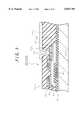
- FIG. 2shows a sectional structure of a matrix portion (display portion) in an active matrix addressing type liquid crystal display device according to a preferred embodiment of the present invention.
- a display panelincludes a TFT substrate TFTSUB composed of a transparent glass substrate SUB1 having one surface on which thin film transistors, pixel electrodes ITO1 and various interconnections are formed; a counter substrate OPSUB composed of a transparent glass substrate SUB2 having one surface on which a common electrode ITO2 and color filters FIL are formed; and a liquid crystal layer LC filled in a gap between the opposed substrates TFTSUB and OPSUB.
- a back light sourceis provided outside the counter substrate OPSUB or the TFT substrate TFTSUB of the liquid crystal panel for permitting a light passing through a pixel portion of the liquid crystal panel to be observed from the side opposite the back light source.
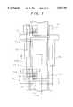
- FIG. 1is a plan view of a pattern of each layer constituting the TFT substrate TFTSUB, showing one pixel and its neighborhood;
- FIG. 2is a sectional view of the display panel, taken on line II--II of FIG. 1; and
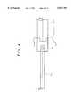
- FIG. 3is a sectional view taken on line III--III of FIG. 1.
- a plurality of parallel gate lines (scanning signal lines or horizontal signal lines) GL and a plurality of parallel data lines (video signal lines or vertical signal lines) DL intersecting a plurality of gate linesare provided on the surface of the TFT substrate.
- a pixel electrode regionis defined by the two adjacent gate lines GL and the two adjacent data lines DL, and a pixel electrode ITO1 is formed over substantially the entire surface of this region.
- a thin film transistor (a region shown by a broken line in FIG. 1) serving as a switching elementis formed in a protruding portion (upward protruding portion in FIG.
- the gate line GLis formed of a conductive film on the transparent glass substrate SUB1, and an insulating film and semiconductor layers are formed thereon to form a thin film transistor TFT (described in detail later).
- a gate voltageis applied to the gate line GL, a channel resistance between a source and a drain (data line DL) in the TFT becomes small.
- the gate voltageis reduced to zero, the channel resistance becomes large.
- a gate insulator GI made of silicon nitrideis provided on the gate electrode constituting a portion of the gate line GL, and an i-type (intrinsic type) semiconductor layer AS made of amorphous silicon doped with no intentional impurity and an n-type semiconductor layer d0 made of amorphous silicon doped with an impurity are formed on the gate insulator GI.
- the i-type semiconductor layer ASfunctions as an active layer of the thin film transistor.
- the source electrode SD1 and a drain electrodeare formed thereon, thus forming a thin film transistor. It is to be noted that a portion of the data line constitutes the drain electrode in this embodiment and the drain electrode is hereinafter referred to as the data line DL unless otherwise specified.
- the gate insulator GIis formed of silicon nitride to a thickness of from 2000 to 5000 ⁇ (about 3500 ⁇ in this embodiment) by, for example, plasma CVD.
- the i-type semiconductor layer ASis formed in thickness of from 500 to 2500 ⁇ (2000 ⁇ in this embodiment).
- the thin n-type semiconductor layer d0is formed of amorphous silicon doped with phosphor (P) in thin thickness of 500 ⁇ or less so as to form an ohmic contact with the i-type semiconductor layer AS.
- each of source and drain electrodesis essentially determined in accordance with a polarity of a voltage applied between the source and drain electrodes.
- the source and drain electrodes in the liquid crystal display device of the present inventionalternate with each other because the polarities are reversed during operation; however, in the following description, one is fixedly called a source electrode and the other is fixedly called the drain electrode for convenience.
- the source electrode SD1is formed of chromium (Cr) on the n-type semiconductor layer d0 in thickness of from 600 to 2000 ⁇ (about 1800 ⁇ in this embodiment).
- the source electrode SD1may be formed of one kind selected from a group consisting of various refractory metals (Ti, Ta, W, Mo) other than Cr and alloys thereof.
- the source electrode SD1is formed on the i-type semiconductor layer AS and the n-type semiconductor layer d0 formed within one pixel region in such a manner that the end portion of the i-type semiconductor layer As extends beyond the end portion of the source electrode SD1 at least in the channel length direction.
- the pixel electrode ITO1is formed of a conductive film on a protective insulating film PSV1 and is connected to the source electrode SD1 through an opening portion (hereinafter, referred to as a contact hole) CN formed in the protective insulating film PSV1.
- the transparent conductive film ITO1can be formed in such a manner as to easily traverse a step formed by the underlying source electrode SD1 without open line defects at the step (described in detail later).
- Such an effectis conspicuous in the case where the pixel electrode ITO1 is made of ITO (indium-tin-oxide) as in this embodiment.
- the etching rate of ITOis larger in grain boundaries than in crystal grains because ITO has a large crystal grain size. Accordingly, the pixel electrode ITO1 tends to be easily broken at a step of the underlying layer unless the cross-section of the underlying layer is smoothed.
- the etching of a semiconductor film using as a mask a metal film on the semiconductor film as described in the Japanese Patent Laid-open No. Sho 61-161764is disadvantageous in that the metal film overhangs in cross-section because it is smaller in etching rate than the semiconductor film, with a result that a transparent conductive film tends to be easily broken at such an overhang.
- a transparent conductive filmtends to be easily broken at such an overhang.
- open line defect probabilities for the pixel electrode ITO1is greatly reduced.
- the pixel electrodeis formed of the transparent conductive film ITO1 made of ITO. This is connected to the source electrode SD1 of the thin film transistor.
- the transparent conductive film ITO1is formed of sputtered ITO in thickness of from 300 to 3000 ⁇ (about 1400 ⁇ in this embodiment).
- the gate line GLis formed of a single layer conductive film.
- the conductive filmis formed of chromium (Cr) by sputtering in thickness of from 600 to 2000 ⁇ (about 1800 ⁇ in this embodiment).
- the gate line GLmay be made from one kind selected from a group consisting of other refractory metals and alloys thereof, like the source electrode SD1.
- the data line DLwhich is the same conductive film as that of the source electrode SD1 is formed on the gate insulator GI and the semiconductor layers As, d0 sequentially formed on the transparent glass substrate SUB1.
- the data line DL and the semiconductor layers As, d0form a stacked structure in cross-section.
- the reason why each layer in the stacked structure has approximately the same patternis due to processing of the i-type semiconductor layer AS using the data line DL as a mask (described later in the paragraph of the manufacturing method).
- the layer mainly contributing to electric conduction and signal transmissionis the conductive layer DL.
- a storage capacity Caddis a capacity formed in a region where a pixel electrode ITO1 of a TFT is overlapped on the gate line GL preceding by one scanning line the gate line GL connected to the TFT with a laminated film of the gate insulator GI and the protective insulating film PSVI interposed therebetween.
- the storage capacity Caddfunctions to reduce the discharge of charges in the capacity of the liquid crystal LC and a decay in its voltage when the TFT is in the OFF state.
- a parasitic capacity Cgsis a capacity in a region where a pixel electrode of a TFT is overlapped on the gate line GL connected to the TFT with a laminated film of the gate insulator GI and the protective insulating film PSVI interposed therebetween. As shown in FIG. 2, the transparent conductive films ITO1 adjacent to each other over the gate line GL are spaced from each other.
- the inventive structure provided with the parasitic capacity Cgseliminates the necessity of covering a gap between the gate line GL and the pixel electrode ITO1 with a black matrix BM otherwise formed on the counter substrate OPSUB, and thereby increasing the aperture ratio of the pixel electrode.
- a light-blocking film SKDwhich is the same conductive film as that of the gate line GL, is formed on the transparent glass substrate SUB1 of the TFT substrate TFTSUB.
- the light-blocking film SKDis overlapped on the pixel electrode ITO1 along the data line DL and further extends under the data line DL, as shown by its layer pattern in FIG. 1.
- the light-blocking film SKDis insulated from the data line DL by the gate insulator GI and the semiconductor layers AS, d0 as shown by the sectional view in FIG. 2, to thereby prevent short-circuit between the light-blocking film SKD and the data line DL.
- the light-blocking film SKDis also insulated from the pixel electrode ITO1 by the gate insulator GI and the protective insulating film PSV1.
- the semiconductor layers AS, d0 interposed, in addition to the gate insulator GI between the light-blocking film SKD and the data line DLare shielded from light illumination and function as insulators, increase a distance between the light-blocking film SKD and the data line DL, and an electrostatic coupling between the light-blocking film SKD and the data line DL is reduced, so that an electrostatic coupling between the data line DL and the pixel electrode ITO1 by way of the light-blocking film SKD is decreased, resulting in reduced cross talk.
- the light-blocking film SKDhas a function to increase an area of a light-transmitting portion, that is, the aperture ratio of a pixel electrode and increase brightness of display as described in detail later.
- a light-transmitting portionthat is, the aperture ratio of a pixel electrode and increase brightness of display as described in detail later.
- the back light source(not shown) is set outside the TFT substrate TFTSUB and an image is observed from the counter substrate OPSUB side
- an illuminating lightpasses through the glass substrate SUB1 and enters the liquid crystal layer LC through a portion on which an interconnection line of sputtered Cr is not formed on one surface of the glass substrate SUB1.
- the transmission of the lightis controlled by a voltage applied between a transparent common electrode ITO2 formed on the counter substrate OPSUB and the pixel electrode ITO1 formed on the TFT substrate TFTSUB.
- the display panelis configured to operate in the normally white mode and is not provided with the light-blocking film SKD and the parasitic capacity Cgs, unlike this embodiment, a wide black matrix is necessary on the counter substrate OPSUB. If the black matrix is not formed in the above case, the area between the pixel electrode ITO1 and the data line DL or the gate line GL transmits the leakage light not controllable by the voltage applied, thus reducing the contrast ratio of the display. Moreover, the counter substrate OPSUB and the TFT substrate TFTSUB are secured together with the liquid crystal therebetween, the large tolerance is necessary in registration of the two substrates and this reduces the aperture ratio as compared with this embodiment in which light-blocking is performed only on the TFT substrate TFTSUB.
- the displaybecomes brighter than the brightness determined by the aperture ratio.
- the semiconductor layers AS and d0are formed under the data line DL, since the semiconductor layers exhibit a light absorbing function, without the light blocking film SKD in back of the semiconductor layers under the data line DL, reflection of light decrease, resulting in dark display.
- the semiconductor layers under the data line DLare processed using the data line DL as a mask, and the conductive film constituting the data line DL does not traverse a step of the semiconductor layer AS, thus reducing open line defect probabilities. Accordingly, the combination of the light-blocking film SKD and the data line DL exhibits a new effect in addition to a bright display.
- the Cr film formed by sputteringis used as the gate line GL and the light-blocking film SKD in this embodiment; however, a multi-layered light-blocking structure with reduced reflection may be used, for which chromium oxide is initially formed on the substrate and then the Cr film is formed by consecutive sputtering.
- the surface of the TFT substrate TFTSUB on the side where the thin film transistor TFT is formedis covered with the protective film PSV1 excluding a contact hole CN for connecting the source electrode SD1 to the pixel electrode ITO1 and a gate terminal portion and a drain terminal portion provided on a peripheral portion of the TFT substrate (described later).
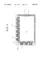
- FIG. 4is a plan view showing a portion ranging from the vicinity of the end of the gate line GL to a gate terminal GTM to be connected to an external drive circuit on the TFT substrate TFTSUB; and FIG. 5 is a sectional view taken on line V--V of FIG. 4.
- the gate terminal GTM formed of the transparent conductive film ITOis exposed to the outside.
- the conductive film of the gate terminal GTMis formed simultaneously with the transparent conductive film ITO1 of the pixel electrode.
- the gate terminal GTMhas a pattern wider than that of the gate line GL for preventing the gate line GL made of chromium from being corroded by permeation of chemicals, water and the like.
- ITOindium-tin-oxide
- ITOindium-tin-oxide
- the use of the gate terminal GTM made of ITO in the liquid crystal display device using TFTsthus makes it possible to ensure a high manufacturing yield and a high reliability.
- FIG. 6is a plan view showing a portion ranging from the vicinity of the end of the data line DL to a drain terminal DTM to be connected to an external drive circuit on the TFT substrate; and FIG. 7 is a sectional view taken on line VII--VII of FIG. 6.
- the drain terminal DTMis formed of the transparent conductive film ITO, like the gate terminal GTM.
- the drain terminal DTMhas a pattern wider than that of the data line DL.
- the protective film PSV1is removed from the drain terminal DTM for connection with an external drive circuit.
- the i-type semiconducting later ASextends longer than the data line DL at the end portion of the data line DL. This is effective to reduce the open line defect probabilities of the drain terminal DTM at the end portion of the data line DL.
- FIG. 8is a plan view showing a schematic structure of a peripheral portion of the display panel PNL.
- a plurality of the gate terminals GTMare arranged correspondingly to a plurality of the gate lines GL, to form a gate terminal group Tg while a plurality of the drain terminals DTM are arranged correspondingly to a plurality of the data lines DL, to form a drain terminal group Td.
- character INJ in FIG. 8designates a portion where a seal pattern SL for securing the TFT substrate TFTSUB and the counter substrate OPSUB together is not provided. After both substrates are secured together, liquid crystal is injected through the portion INJ.
- color filters FIL for red, green and blue, a protective film PSV2, the transparent common electrode ITO2 and an orienting film ORI2are sequentially formed on one surface of the transparent glass substrate SUB2.
- a polarizer POL2is attached on the other surface of the transparent glass substrate SUB2, and with a polarizer POL1 is attached on the surface of the TFT substrate TFTSUB on the side where the TFTs are not formed, for polarizing and analyzing a light, respectively.
- a light-blocking black matrix BMis not formed on the glass substrate SUB2 shown in FIG. 2, in actual practice there is a black matrix formed of a sputtered Cr film, a stacked layer of Cr oxide and Cr, or a resin film disposed at a position corresponding to the TFT portion in FIG. 1.
- FIG. 9is a flow chart showing the flow of steps (A) to (F) for making the TFT substrate TFTSUB; and FIGS. 10 to 15 show sectional structures of the liquid crystal display device in the steps (A) to (F), respectively.
- FIG. 11shows the sectional structure directly after a thin film is etched in each step excluding the step (B), and a photoresist used as a mask is left on the thin film in each cross-section for convenience of explanation.
- Each figureis a sectional view of a portion in the vicinity of a connection portion of the thin film transistor and a pixel electrode on the TFT substrate TFTSUB (see the sectional view of FIG. 3).
- the sectional structure of the liquid crystal display device processed in the final step shown in FIG. 9corresponds to that shown in FIG. 3.
- Each of the steps (A), (C), (D), (E) and (F)includes a photolithograph processing.
- the photolithographic processing in the present inventionincludes a series of processes of coating photoresist, selective exposure using a mask and development. As can be seen from FIG. 9, the photolithographic processing is repeated five times until the TFT substrate is finished.
- a transparent glass substrate SUB1is prepared, and a Cr film is formed on one surface of the transparent glass substrate SUB1 by sputtering.
- a mask of a photoresist PRESis formed in a specified pattern on the Cr film by a first photolithography processing, and the Cr film is selectively etched using the mask, to obtain a conductive film having the specified pattern.
- This conductive filmforms a gate line GL or a light-blocking film SKD.
- a silicon nitride film GI, an i-type amorphous Si film AS and an n-type amorphous Si film d0are sequentially formed on the Cr film provided on the transparent glass substrate SUB1 by plasma CVD, and then a Cr film as a first conductive film d1 is formed thereon by sputtering.
- the semiconductor films AS, d0are consecutively formed without a photoresist step, to reduce surface oxidation of the semiconductor layers due to the resist. This is effective to lower a contact resistance between the n-type semiconductor layer d0 and the conductive film d1 and hence to increase electron mobility in the thin film transistor.
- a mask of the photoresist PRESis formed in a specified pattern on the Cr film (d1) by a second photolithography processing, and the Cr film is selectively etched, to form the specified pattern. Subsequently, the n-type semiconductor layer d0 in the opening is removed by dry etching using the photoresist PRES.
- the end portion of the Cr filmgenerally retracts by a value from of 0.5 to 1 ⁇ m from the end portion of the photoresist PRES. Also, due to anisotropic dry etching of the n-type semiconductor layer d0 and its very small thickness of 500 ⁇ or less as described above, the end portion of the n-type semiconductor layer d0 retracts only by about 0.3 ⁇ m from the end portion of the photoresist PRES. As a result, the layer underlying the source electrode SD1 is not etched, and thereby the SD1 does not overhang.
- a mask of another photoresist PRESis then formed in a specified pattern by a third photolithography processing, and the i-type semiconductor layer AS is selectively removed by etching on the gate insulator GI.
- the above photoresist PRESis patterned in such a manner as to be wider than that of the source electrode SD1 at its end portion for the etched i-type semiconductor layer AS to provide a stair case shape at a circled portion A in FIG. 13. This is effective to prevent open line defects of the transparent conductive film subsequently formed above the source electrode at its end portion.
- the photoresist PRESis not formed on most of the data line shown in FIG. 2, and the semiconductor layers underlying the data line are etched using as a mask the conductive film d1 of the data line DL.
- the i-type semiconductor layer ASdoes not protrude from under the data line near the data line having no photoresist PRES thereon. This enables high precision processing, and is effective to improve the aperture ratio, and to reduce a gate capacity to shorten a delay time caused by the gate line.
- the experiments by the present inventorshowed that in the case where the pattern of the photoresist PRES for etching the i-type semiconductor layer AS is not set to be wider than that of the source electrode SD1 and the i-type semiconductor layer AS is etched using as a mask the conductive film d1 of the source electrode, the underlying semiconductor layer retracts from the end portion of the source electrode SD1 and cause by overhangs because the thickness of the i-type semiconducting layer AS is larger than the n-type semiconductor layer d0, with a result that the pixel electrode ITO subsequently formed above the source electrode increases its open line defect probabilities greatly at a step caused by the overhang.
- the protective insulating film PSV1 made of silicon nitrideis formed by plasma CVD.
- a mask of another photoresist PRESis formed by a fourth photolithography processing, and the protective insulating film PSV1 is removed by etching at the contact hole CN and connection terminal portions.
- a second conductive film d2 made of ITOis formed by sputtering.
- a mask of another photoresist PRESis formed in a specified pattern on the second conductive film d2, and the second conductive film d2 is selectively etched to form a pattern of the pixel electrode ITO1 and the like.
- the semiconductor layers AS, d0, in addition to the gate insulator GI, interposed between the light-blocking film SKD and the data line DLare shielded from light illumination and function as insulators, and further increases a distance between the light-blocking film SKD and the data line DL, and an electrostatic coupling between the light-blocking film SKD and the data line DL is reduced, so that an electrostatic coupling between the data line DL and the pixel electrode ITO1 by way of the light-blocking film SKD is decreased, resulting in the reduced cross talk.
- the present inventionthus can provide a liquid crystal display device capable of a display of higher brightness due to higher aperture ratio, of high contrast and low cross talk.
- the present inventioncan provide an inexpensive liquid crystal display device in which a TFT substrate constituting a display panel can be made in a simple process including five photolithography process steps, and a method of making the same.
- the present inventioncan provide a liquid crystal display device capable of higher manufacturing yield by preventing open line defects of a conductive film made of ITO at a step caused by the underlying layer.
Landscapes
- Physics & Mathematics (AREA)
- Nonlinear Science (AREA)
- Mathematical Physics (AREA)
- Chemical & Material Sciences (AREA)
- Crystallography & Structural Chemistry (AREA)
- General Physics & Mathematics (AREA)
- Optics & Photonics (AREA)
- Engineering & Computer Science (AREA)
- Microelectronics & Electronic Packaging (AREA)
- Liquid Crystal (AREA)
- Thin Film Transistor (AREA)
Abstract
Description
Claims (5)
Priority Applications (14)
| Application Number | Priority Date | Filing Date | Title |
|---|---|---|---|
| US09/207,742US6377323B1 (en) | 1995-07-25 | 1998-12-08 | Liquid crystal display device and method of making same |
| US09/342,173US6275278B1 (en) | 1996-07-19 | 1999-06-29 | Liquid crystal display device and method of making same |
| US09/717,265US6424389B1 (en) | 1995-07-25 | 2000-11-22 | Fabrication method of liquid crystal display device |
| US10/118,081US6590623B2 (en) | 1995-07-25 | 2002-04-09 | Fabrication method of liquid crystal display device having a reduced number of process steps |
| US10/158,902US6667778B1 (en) | 1995-07-25 | 2002-06-03 | Liquid crystal display device having a transparent conductive film formed on an insulating film |
| US10/660,696US6839106B2 (en) | 1995-07-25 | 2003-09-12 | Liquid crystal display device and method of making same |
| US10/990,497US7271870B2 (en) | 1995-07-25 | 2004-11-18 | Liquid crystal display device and method of making same |
| US11/338,853US7375786B2 (en) | 1995-07-25 | 2006-01-25 | Liquid crystal display device and method of making same |
| US11/929,159US7535536B2 (en) | 1995-07-25 | 2007-10-30 | Display device |
| US11/929,085US7450192B2 (en) | 1995-07-25 | 2007-10-30 | Display device |
| US11/929,025US7605900B2 (en) | 1995-07-25 | 2007-10-30 | Liquid crystal display device |
| US12/562,636US7907225B2 (en) | 1995-07-25 | 2009-09-18 | Liquid crystal display device |
| US13/037,925US8107028B2 (en) | 1995-07-25 | 2011-03-01 | Display device having improved step coverage for thin film transistors |
| US13/308,684US8421943B2 (en) | 1995-07-25 | 2011-12-01 | Liquid crystal display device having a third electrode formed over a second insulating film and overlapped with a pair of gate lines |
Applications Claiming Priority (2)
| Application Number | Priority Date | Filing Date | Title |
|---|---|---|---|
| JP18878395AJP3866783B2 (en) | 1995-07-25 | 1995-07-25 | Liquid crystal display |
| JP7-188783 | 1995-07-25 |
Related Child Applications (1)
| Application Number | Title | Priority Date | Filing Date |
|---|---|---|---|
| US09/207,742ContinuationUS6377323B1 (en) | 1995-07-25 | 1998-12-08 | Liquid crystal display device and method of making same |
Publications (1)
| Publication Number | Publication Date |
|---|---|
| US5847781Atrue US5847781A (en) | 1998-12-08 |
Family
ID=16229721
Family Applications (14)
| Application Number | Title | Priority Date | Filing Date |
|---|---|---|---|
| US08/683,408Expired - LifetimeUS5847781A (en) | 1995-07-25 | 1996-07-19 | Liquid crystal display device comprises a light-blocking layer and a plurality of data lines which have a width that is larger than the width of a semiconductor layer |
| US09/207,742Expired - LifetimeUS6377323B1 (en) | 1995-07-25 | 1998-12-08 | Liquid crystal display device and method of making same |
| US09/717,265Expired - LifetimeUS6424389B1 (en) | 1995-07-25 | 2000-11-22 | Fabrication method of liquid crystal display device |
| US10/118,081Expired - LifetimeUS6590623B2 (en) | 1995-07-25 | 2002-04-09 | Fabrication method of liquid crystal display device having a reduced number of process steps |
| US10/158,902Expired - LifetimeUS6667778B1 (en) | 1995-07-25 | 2002-06-03 | Liquid crystal display device having a transparent conductive film formed on an insulating film |
| US10/660,696Expired - LifetimeUS6839106B2 (en) | 1995-07-25 | 2003-09-12 | Liquid crystal display device and method of making same |
| US10/990,497Expired - Fee RelatedUS7271870B2 (en) | 1995-07-25 | 2004-11-18 | Liquid crystal display device and method of making same |
| US11/338,853Expired - Fee RelatedUS7375786B2 (en) | 1995-07-25 | 2006-01-25 | Liquid crystal display device and method of making same |
| US11/929,025Expired - Fee RelatedUS7605900B2 (en) | 1995-07-25 | 2007-10-30 | Liquid crystal display device |
| US11/929,159Expired - Fee RelatedUS7535536B2 (en) | 1995-07-25 | 2007-10-30 | Display device |
| US11/929,085Expired - Fee RelatedUS7450192B2 (en) | 1995-07-25 | 2007-10-30 | Display device |
| US12/562,636Expired - Fee RelatedUS7907225B2 (en) | 1995-07-25 | 2009-09-18 | Liquid crystal display device |
| US13/037,925Expired - Fee RelatedUS8107028B2 (en) | 1995-07-25 | 2011-03-01 | Display device having improved step coverage for thin film transistors |
| US13/308,684Expired - Fee RelatedUS8421943B2 (en) | 1995-07-25 | 2011-12-01 | Liquid crystal display device having a third electrode formed over a second insulating film and overlapped with a pair of gate lines |
Family Applications After (13)
| Application Number | Title | Priority Date | Filing Date |
|---|---|---|---|
| US09/207,742Expired - LifetimeUS6377323B1 (en) | 1995-07-25 | 1998-12-08 | Liquid crystal display device and method of making same |
| US09/717,265Expired - LifetimeUS6424389B1 (en) | 1995-07-25 | 2000-11-22 | Fabrication method of liquid crystal display device |
| US10/118,081Expired - LifetimeUS6590623B2 (en) | 1995-07-25 | 2002-04-09 | Fabrication method of liquid crystal display device having a reduced number of process steps |
| US10/158,902Expired - LifetimeUS6667778B1 (en) | 1995-07-25 | 2002-06-03 | Liquid crystal display device having a transparent conductive film formed on an insulating film |
| US10/660,696Expired - LifetimeUS6839106B2 (en) | 1995-07-25 | 2003-09-12 | Liquid crystal display device and method of making same |
| US10/990,497Expired - Fee RelatedUS7271870B2 (en) | 1995-07-25 | 2004-11-18 | Liquid crystal display device and method of making same |
| US11/338,853Expired - Fee RelatedUS7375786B2 (en) | 1995-07-25 | 2006-01-25 | Liquid crystal display device and method of making same |
| US11/929,025Expired - Fee RelatedUS7605900B2 (en) | 1995-07-25 | 2007-10-30 | Liquid crystal display device |
| US11/929,159Expired - Fee RelatedUS7535536B2 (en) | 1995-07-25 | 2007-10-30 | Display device |
| US11/929,085Expired - Fee RelatedUS7450192B2 (en) | 1995-07-25 | 2007-10-30 | Display device |
| US12/562,636Expired - Fee RelatedUS7907225B2 (en) | 1995-07-25 | 2009-09-18 | Liquid crystal display device |
| US13/037,925Expired - Fee RelatedUS8107028B2 (en) | 1995-07-25 | 2011-03-01 | Display device having improved step coverage for thin film transistors |
| US13/308,684Expired - Fee RelatedUS8421943B2 (en) | 1995-07-25 | 2011-12-01 | Liquid crystal display device having a third electrode formed over a second insulating film and overlapped with a pair of gate lines |
Country Status (4)
| Country | Link |
|---|---|
| US (14) | US5847781A (en) |
| JP (1) | JP3866783B2 (en) |
| KR (2) | KR100245973B1 (en) |
| TW (1) | TW331598B (en) |
Cited By (89)
| Publication number | Priority date | Publication date | Assignee | Title |
|---|---|---|---|---|
| US6038003A (en)* | 1997-06-11 | 2000-03-14 | Lg. Philips Lcd Co., Ltd. | Liquid crystal display and method of manufacturing the same |
| US6057896A (en)* | 1996-11-26 | 2000-05-02 | Samsung Electronics Co., Ltd. | Liquid crystal displays using organic insulating material for a passivation layer and/or a gate insulating layer and manufacturing methods thereof |
| US6081315A (en)* | 1998-05-07 | 2000-06-27 | Nec Corporation | Liquid crystal display apparatus |
| US6177970B1 (en)* | 1997-09-25 | 2001-01-23 | Samsung Electronics Co., Ltd. | In-plane switching mode liquid crystal display and a method manufacturing the same |
| US6195140B1 (en)* | 1997-07-28 | 2001-02-27 | Sharp Kabushiki Kaisha | Liquid crystal display in which at least one pixel includes both a transmissive region and a reflective region |
| US6275278B1 (en) | 1996-07-19 | 2001-08-14 | Hitachi, Ltd. | Liquid crystal display device and method of making same |
| US6278503B1 (en)* | 1999-01-20 | 2001-08-21 | Sanyo Electric Co., Ltd. | Vertical orientation type liquid crystal display having conductive film reducing the influence of electrical field caused by the storage capacitor line on the liquid crystal |
| US6330047B1 (en) | 1997-07-28 | 2001-12-11 | Sharp Kabushiki Kaisha | Liquid crystal display device and method for fabricating the same |
| US6335772B1 (en)* | 1999-05-18 | 2002-01-01 | Sony Corporation | Apparatus and method for a liquid crystal display device having an electrically-conductive light-shading layer formed on a smoothed layer |
| US6373546B1 (en)* | 1997-03-03 | 2002-04-16 | Lg Philips Lcd Co., Ltd. | Structure of a liquid crystal display and the method of manufacturing the same |
| US6377323B1 (en)* | 1995-07-25 | 2002-04-23 | Hitachi, Ltd. | Liquid crystal display device and method of making same |
| US20020050967A1 (en)* | 2000-10-27 | 2002-05-02 | Hitachi, Ltd. | Liquid crystal display device |
| US6396554B1 (en)* | 1999-01-29 | 2002-05-28 | Sanyo Electric Co., Ltd. | Color liquid crystal display with reduced data line wiring |
| US20020080300A1 (en)* | 2000-12-23 | 2002-06-27 | Lee Joun Ho | Liquid crystal display and manufacturing method of the same |
| US6414730B1 (en)* | 1998-10-26 | 2002-07-02 | Sharp Kabushiki Kaisha | Liquid crystal display device and method for manufacturing the same |
| US6525788B1 (en)* | 1998-10-21 | 2003-02-25 | Advanced Display Inc. | Liquid crystal display device |
| US20030102424A1 (en)* | 1999-01-14 | 2003-06-05 | Sharp Kabushiki Kaisha. | Two-dimensional image detector, active-matrix substrate, and display device |
| US6697139B1 (en)* | 1999-03-25 | 2004-02-24 | Hitachi, Ltd. | Liquid crystal display device having particular stacked layered structure at peripheral portion |
| US20040046905A1 (en)* | 1999-09-30 | 2004-03-11 | Hong Mun-Pyo | Thin film transistor array panel for a liquid crystal display and methods for manufacturing the same |
| US20040066472A1 (en)* | 2002-10-05 | 2004-04-08 | Lg.Philips Lcd Co.Ltd. | Liquid crystal display panel and method of fabricating the same |
| US6741315B1 (en)* | 1999-08-27 | 2004-05-25 | Seiko Epson Corporation | Liquid crystal device and electronic apparatus |
| US20040105042A1 (en)* | 2002-10-01 | 2004-06-03 | Shui Huang | [pixel structure and fabricating method thereof] |
| US20040229393A1 (en)* | 2003-05-12 | 2004-11-18 | Han-Chung Lai | Flat panel display and fabrication method thereof |
| US20050174846A1 (en)* | 2003-12-03 | 2005-08-11 | Chul-Ho Kim | Thin film transistor array panel for display |
| US20050185109A1 (en)* | 1996-11-26 | 2005-08-25 | Soo-Guy Rho | Liquid crystal displays using organic insulating material and manufacturing methods thereof |
| US20050190315A1 (en)* | 2002-07-30 | 2005-09-01 | Hiroaki Asuma | Liquid crystal display device |
| US20050230719A1 (en)* | 2002-03-19 | 2005-10-20 | Advanced Display Inc. | Display apparatus |
| US20050263769A1 (en)* | 2004-05-27 | 2005-12-01 | Byung Chul Ahn | Liquid crystal display device and fabricating method thereof |
| US20050263768A1 (en)* | 2004-05-27 | 2005-12-01 | Lg. Philips Lcd Co., Ltd. | Liquid crystal display device and fabricating method thereof |
| US20050270450A1 (en)* | 2004-06-05 | 2005-12-08 | Ahn Byung C | Liquid crystal display device and fabricating method thereof |
| US20050270454A1 (en)* | 2004-06-05 | 2005-12-08 | Ahn Byung C | Liquid crystal display device and fabricating method thereof |
| US20050270453A1 (en)* | 2004-06-05 | 2005-12-08 | Lg. Philips Lcd Co., Ltd. | Liquid crystal display device and fabricating method thereof |
| US20050270451A1 (en)* | 2004-06-05 | 2005-12-08 | Ahn Byung C | Liquid crystal display device and fabricating method thereof |
| US20050270452A1 (en)* | 2004-06-05 | 2005-12-08 | Ahn Byung C | Liquid crystal display device and method of fabricating same |
| US20050270434A1 (en)* | 2004-06-05 | 2005-12-08 | Jung Tae Y | Liquid crystal display device and fabricating method thereof |
| US20050269638A1 (en)* | 2004-06-05 | 2005-12-08 | Jung Tae Y | Liquid crystal display device and fabricating method thereof |
| US20060001604A1 (en)* | 2003-01-03 | 2006-01-05 | Hee-Seob Kim | Thin film transistor panel for liquid crystal display |
| US20060017054A1 (en)* | 2004-06-24 | 2006-01-26 | Ahn Byung C | Liquid crystal display device and fabricating method thereof |
| US20060028494A1 (en)* | 2002-12-30 | 2006-02-09 | Koninklijke Philips Electronics N.V. | Optical display driving method |
| US20060119771A1 (en)* | 2004-12-04 | 2006-06-08 | Lim Joo S | Liquid crystal display device and fabricating method thereof |
| US20060138417A1 (en)* | 2004-12-24 | 2006-06-29 | Ahn Byung C | Liquid crystal display device and fabricating method thereof |
| US20060139504A1 (en)* | 2004-12-24 | 2006-06-29 | Ahn Byung C | Liquid crystal display device and fabricating method thereof |
| US20060139548A1 (en)* | 2004-12-24 | 2006-06-29 | Ahn Byung C | Liquid crystal display device and fabricating method thereof |
| US20060139554A1 (en)* | 2004-12-23 | 2006-06-29 | Park Jong W | Liquid crystal display panel and fabricating method thereof |
| US20060138428A1 (en)* | 2004-12-24 | 2006-06-29 | Ahn Byung C | Liquid crystal display device and fabricating method thereof, and thin film patterning method applied thereto |
| US20060139502A1 (en)* | 2004-12-24 | 2006-06-29 | Ahn Byung C | Liquid crystal display device and fabricating method thereof |
| US20060139556A1 (en)* | 2004-12-23 | 2006-06-29 | Ahn Byung C | Liquid crystal display panel and method of fabricating the same |
| US20060146216A1 (en)* | 2004-12-31 | 2006-07-06 | Ahn Byung C | Liquid crystal display device and fabricating method thereof |
| US20060146212A1 (en)* | 2004-12-31 | 2006-07-06 | Ahn Byung C | Liquid crystal display device and fabricating method thereof |
| US20060146217A1 (en)* | 2004-12-31 | 2006-07-06 | Ahn Byung C | Liquid crystal display device and fabricating method thereof |
| US20060146213A1 (en)* | 2004-12-31 | 2006-07-06 | Ahn Byung C | Liquid crystal display device and fabricating method thereof |
| US20060145161A1 (en)* | 2004-12-31 | 2006-07-06 | Ji No Lee | Liquid crystal display device and method for fabricating the same |
| US20060146245A1 (en)* | 2004-12-31 | 2006-07-06 | Ahn Byung C | Liquid crystal display device and fabricating method thereof |
| US20060290867A1 (en)* | 2005-06-27 | 2006-12-28 | Ahn Byung C | Liquid crystal display and fabricating method thereof |
| US20070000431A1 (en)* | 2005-06-30 | 2007-01-04 | Lg.Philips Lcd Co., Ltd. | Method of repairing a short defect and a method of fabricating a liquid crystal display device |
| US20070002249A1 (en)* | 2005-06-30 | 2007-01-04 | Yoo Soon S | Liquid crystal display device and fabricating method thereof |
| US20070001979A1 (en)* | 2005-06-30 | 2007-01-04 | Lg Philips Lcd Co., Ltd. | Method of forming fine pattern, liquid crystal display device having a fine pattern and fabricating method thereof |
| US20070008473A1 (en)* | 2002-10-16 | 2007-01-11 | Lg Philips Lcd Co., Ltd. | Liquid crystal display device |
| US20070024770A1 (en)* | 2002-12-23 | 2007-02-01 | Sang-Min Jang | Liquid crystal display device and method of fabricating the same |
| US20070109469A1 (en)* | 2005-11-11 | 2007-05-17 | Samsung Electronics Co., Ltd. | Liquid crystal display device and method of fabricating the same |
| US20070146606A1 (en)* | 2005-12-28 | 2007-06-28 | Lg.Philips Lcd Co., Ltd. | Liquid crystal display device and method of driving the same |
| US20070165175A1 (en)* | 2005-12-28 | 2007-07-19 | Nagayama Kazuyoshi | Liquid crystal display device |
| US20070165173A1 (en)* | 2005-12-28 | 2007-07-19 | Nagayama Kazuyoshi | Liquid crystal display device |
| US20070165174A1 (en)* | 2005-12-28 | 2007-07-19 | Nagayama Kazuyoshi | Liquid crystal display device and method of fabricating the same |
| US20070176872A1 (en)* | 2005-12-28 | 2007-08-02 | Lg.Philips Lcd Co.,Ltd. | Liquid crystal display device |
| US20070188691A1 (en)* | 2005-12-28 | 2007-08-16 | Lg.Philips Lcd Co., Ltd. | Liquid crystal display device and method of fabricating thereof |
| US7259806B1 (en)* | 1999-08-07 | 2007-08-21 | Lg.Philips Lcd Co., Ltd. | Liquid crystal display device with light absorbing layers |
| US20070200989A1 (en)* | 2005-12-28 | 2007-08-30 | Lg.Philips Lcd Co., Ltd. | Liquid crystal display device and the method thereof |
| US20080017886A1 (en)* | 2006-07-18 | 2008-01-24 | Samsung Electronics Co., Ltd. | Thin film transistor array panel |
| US20080017864A1 (en)* | 2006-07-21 | 2008-01-24 | Samsung Electronics Co., Ltd. | Display substrate, display device having the same and method of manufacturing the same |
| US20080030638A1 (en)* | 2002-06-03 | 2008-02-07 | Dong-Gyu Kim | Thin film transistor array panel for liquid crystal display having pixel electrode |
| US20080121415A1 (en)* | 2006-11-27 | 2008-05-29 | Lg.Philips Lcd Co., Ltd. | Method for manufacturing flexible display device and flexible display device |
| CN100410788C (en)* | 2005-01-19 | 2008-08-13 | 友达光电股份有限公司 | pixel structure |
| US20080309839A1 (en)* | 2004-02-06 | 2008-12-18 | Dong-Gyu Kim | Thin film transistor array panel and liquid crystal display including the panel |
| US20090166633A1 (en)* | 2007-12-28 | 2009-07-02 | Samsung Electronics Co., Ltd. | Array substrate and method for manufacturing the same |
| US7643122B2 (en) | 2004-06-30 | 2010-01-05 | Lg Display Co., Ltd. | LCD device having data line disposed within, and data link disposed outside liquid crystal region and crossing a sealant region and with gate insulating film in contact with upper surface of the data link |
| US20100019244A1 (en)* | 2006-09-11 | 2010-01-28 | Lg Display Co., Ltd. | Method for fabricating thin film pattern, liquid crystal display panel and method for fabricating thereof using the same |
| US20100214792A1 (en)* | 2007-03-13 | 2010-08-26 | Chen Chia-Li | Luminous pedal for a bicycle |
| US20100237348A1 (en)* | 2009-03-19 | 2010-09-23 | Au Optronics Corporation | Thin Film Transistor Array Substrate |
| US20100253605A1 (en)* | 2009-04-01 | 2010-10-07 | Tpo Displays Corp. | Display device |
| US7995172B2 (en) | 2006-05-31 | 2011-08-09 | Nec Lcd Technologies, Ltd. | Semitransparent liquid crystal display |
| US8064024B2 (en) | 2004-12-04 | 2011-11-22 | Lg Display Co., Ltd. | Transflective thin film transistor substrate of liquid crystal display device having a contact electrode connecting a data link to a data line |
| US20110292312A1 (en)* | 2010-05-28 | 2011-12-01 | Samsung Mobile Display Co., Ltd. | Liquid crystal display device and manufacturing method thereof |
| US8179505B2 (en) | 2004-12-23 | 2012-05-15 | Lg Display Co., Ltd. | Transflective type liquid crystal display device having a color layer in the transmissive region and a non-color layer in the reflective region and fabricating method thereof |
| US20150008436A1 (en)* | 2013-07-05 | 2015-01-08 | Samsung Display Co., Ltd. | Display substrate and method of manufacturing the same |
| US9099361B2 (en) | 2000-04-27 | 2015-08-04 | Semiconductor Energy Laboratory Co., Ltd. | Semiconductor device and method of fabricating the same |
| EP2947507A1 (en)* | 2014-05-21 | 2015-11-25 | InnoLux Corporation | Display device |
| US9494815B2 (en)* | 2012-12-24 | 2016-11-15 | Shanghai Tianma Micro-electronics Co., Ltd. | TN liquid crystal display device and touch control method thereof |
| US11977303B2 (en) | 2022-02-02 | 2024-05-07 | Japan Display Inc. | Display device |
Families Citing this family (49)
| Publication number | Priority date | Publication date | Assignee | Title |
|---|---|---|---|---|
| JP3208658B2 (en)* | 1997-03-27 | 2001-09-17 | 株式会社アドバンスト・ディスプレイ | Manufacturing method of electro-optical element |
| KR100477128B1 (en)* | 1997-08-25 | 2005-07-18 | 삼성전자주식회사 | Thin Film Transistor Board for Liquid Crystal Display with Light-Blocking Film |
| KR100537882B1 (en)* | 1997-08-25 | 2006-03-14 | 삼성전자주식회사 | LCD and its manufacturing method |
| JP5043072B2 (en)* | 1997-10-14 | 2012-10-10 | 三星電子株式会社 | Substrate for liquid crystal display device, liquid crystal display device and method for manufacturing the same |
| JP4643774B2 (en)* | 1997-10-18 | 2011-03-02 | 三星電子株式会社 | Liquid crystal display device and manufacturing method thereof |
| KR100528883B1 (en)* | 1998-06-13 | 2006-02-28 | 엘지.필립스 엘시디 주식회사 | Manufacturing method of liquid crystal display device |
| KR100303446B1 (en)* | 1998-10-29 | 2002-10-04 | 삼성전자 주식회사 | Manufacturing method of thin film transistor substrate for liquid crystal display device |
| US6900854B1 (en)* | 1998-11-26 | 2005-05-31 | Samsung Electronics Co., Ltd. | Thin film transistor array panel for a liquid crystal display |
| KR100474003B1 (en)* | 1998-11-27 | 2005-09-16 | 엘지.필립스 엘시디 주식회사 | Liquid crystal display device |
| US6657695B1 (en)* | 1999-06-30 | 2003-12-02 | Samsung Electronics Co., Ltd. | Liquid crystal display wherein pixel electrode having openings and protrusions in the same substrate |
| KR100351874B1 (en)* | 1999-09-14 | 2002-09-12 | 엘지.필립스 엘시디 주식회사 | Thin film transistor liquid crystal display device |
| KR100635943B1 (en)* | 1999-11-04 | 2006-10-18 | 삼성전자주식회사 | Thin film transistor substrate and manufacturing method thereof |
| KR100709704B1 (en)* | 2000-05-12 | 2007-04-19 | 삼성전자주식회사 | Thin film transistor substrate for liquid crystal display device and manufacturing method thereof |
| KR100695299B1 (en) | 2000-05-12 | 2007-03-14 | 삼성전자주식회사 | Thin film transistor substrate for liquid crystal display device and manufacturing method thereof |
| US6624856B2 (en)* | 2000-07-07 | 2003-09-23 | Casio Computer Co., Ltd. | Liquid crystal display device having thin film transistors for reducing leak current |
| JP2002107743A (en)* | 2000-09-25 | 2002-04-10 | Koninkl Philips Electronics Nv | Reflection type liquid crystal display device |
| KR100582598B1 (en) | 2000-10-25 | 2006-05-23 | 엘지.필립스 엘시디 주식회사 | LCD to prevent light leakage |
| KR100448043B1 (en)* | 2000-12-01 | 2004-09-10 | 비오이 하이디스 테크놀로지 주식회사 | Fringe field switching mode lcd removed light leakage |
| TW490857B (en)* | 2001-02-05 | 2002-06-11 | Samsung Electronics Co Ltd | Thin film transistor array substrate for liquid crystal display and method of fabricating same |
| US6833900B2 (en)* | 2001-02-16 | 2004-12-21 | Seiko Epson Corporation | Electro-optical device and electronic apparatus |
| KR100475636B1 (en)* | 2001-08-20 | 2005-03-10 | 엘지.필립스 엘시디 주식회사 | Method for fabricating of an array substrate for LCD |
| JP2003172919A (en)* | 2001-12-06 | 2003-06-20 | Matsushita Electric Ind Co Ltd | Liquid crystal display |
| KR100881358B1 (en)* | 2001-12-28 | 2009-02-04 | 엘지디스플레이 주식회사 | Liquid crystal display |
| JP2003280029A (en)* | 2002-03-25 | 2003-10-02 | Alps Electric Co Ltd | Liquid crystal display device |
| KR100480333B1 (en)* | 2002-04-08 | 2005-04-06 | 엘지.필립스 엘시디 주식회사 | Array substrate for a liquid crystal display device and Method for fabricating of the same |
| US7053971B2 (en)* | 2002-07-17 | 2006-05-30 | Citzen Watch Co., Ltd. | Liquid crystal display panel |
| KR100905472B1 (en) | 2002-12-17 | 2009-07-02 | 삼성전자주식회사 | Thin film transistor array substrate and liquid crystal display including the same |
| US20040174483A1 (en)* | 2003-03-07 | 2004-09-09 | Yayoi Nakamura | Liquid crystal display device having auxiliary capacitive electrode |
| JP2005091819A (en)* | 2003-09-18 | 2005-04-07 | Sharp Corp | Liquid crystal display |
| KR100796592B1 (en)* | 2005-08-26 | 2008-01-21 | 삼성에스디아이 주식회사 | Thin film transistor and its manufacturing method |
| US7821613B2 (en)* | 2005-12-28 | 2010-10-26 | Semiconductor Energy Laboratory Co., Ltd. | Display device and manufacturing method thereof |
| KR101229413B1 (en)* | 2006-04-18 | 2013-02-04 | 엘지디스플레이 주식회사 | An array substrate for In-Plane switching mode LCD and method of fabricating of the same |
| KR101373735B1 (en) | 2007-02-22 | 2014-03-14 | 삼성디스플레이 주식회사 | Method for manufacturing a aisnal line, thin film transistor array panel and method for manufacturing the same |
| JP2007193371A (en)* | 2007-04-26 | 2007-08-02 | Advanced Display Inc | Liquid crystal display device |
| US8101442B2 (en)* | 2008-03-05 | 2012-01-24 | Semiconductor Energy Laboratory Co., Ltd. | Method for manufacturing EL display device |
| US8841661B2 (en)* | 2009-02-25 | 2014-09-23 | Semiconductor Energy Laboratory Co., Ltd. | Staggered oxide semiconductor TFT semiconductor device and manufacturing method thereof |
| CN102156359B (en)* | 2010-06-13 | 2014-05-07 | 京东方科技集团股份有限公司 | Array base plate, liquid crystal panel, liquid crystal display and driving method |
| CN102446913A (en)* | 2010-09-30 | 2012-05-09 | 北京京东方光电科技有限公司 | Array baseplate and manufacturing method thereof and liquid crystal display |
| JP2012222261A (en)* | 2011-04-13 | 2012-11-12 | Mitsubishi Electric Corp | Transistor, manufacturing method of the same and display device |
| KR101798868B1 (en)* | 2011-06-24 | 2017-12-20 | 엘지디스플레이 주식회사 | Liquid crystal display device and method for manufacturing the same |
| JP5794013B2 (en)* | 2011-07-22 | 2015-10-14 | セイコーエプソン株式会社 | Electro-optical device and electronic apparatus |
| KR20130066247A (en) | 2011-12-12 | 2013-06-20 | 삼성디스플레이 주식회사 | Thin film transistor display panel and manufacturing method thereof |
| CN103576401B (en)* | 2012-08-10 | 2018-05-08 | 北京京东方光电科技有限公司 | A kind of array base palte and preparation method thereof, display device |
| CN103197478B (en)* | 2013-03-20 | 2015-11-25 | 合肥京东方光电科技有限公司 | A kind of array base palte and liquid crystal indicator |
| KR102198111B1 (en)* | 2013-11-04 | 2021-01-05 | 삼성디스플레이 주식회사 | Thin film transistor array panel and manufacturing method thereof |
| CN103676386B (en)* | 2013-12-27 | 2016-10-05 | 京东方科技集团股份有限公司 | A kind of display floater and display device |
| KR101556160B1 (en)* | 2015-01-07 | 2015-10-02 | 삼성디스플레이 주식회사 | Thin film transistor array panel |
| KR102345474B1 (en)* | 2015-05-11 | 2021-12-31 | 삼성디스플레이 주식회사 | Display device |
| KR102596770B1 (en)* | 2016-12-05 | 2023-11-01 | 삼성디스플레이 주식회사 | Liquid crystal display device |
Citations (7)
| Publication number | Priority date | Publication date | Assignee | Title |
|---|---|---|---|---|
| US4789223A (en)* | 1985-03-28 | 1988-12-06 | Kabushiki Kaisha Toshiba | Matrix-addressed liquid crystal display device with compensation for potential shift of pixel electrodes |
| US4984033A (en)* | 1986-04-02 | 1991-01-08 | Mitsubishi Denki Kabushiki Kaisha | Thin film semiconductor device with oxide film on insulating layer |
| US5047819A (en)* | 1988-02-26 | 1991-09-10 | Seikosha Co., Ltd. | Amorphous-silicon thin film transistor array substrate |
| US5055899A (en)* | 1987-09-09 | 1991-10-08 | Casio Computer Co., Ltd. | Thin film transistor |
| US5317433A (en)* | 1991-12-02 | 1994-05-31 | Canon Kabushiki Kaisha | Image display device with a transistor on one side of insulating layer and liquid crystal on the other side |
| US5414547A (en)* | 1991-11-29 | 1995-05-09 | Seiko Epson Corporation | Liquid crystal display device and manufacturing method therefor |
| US5610737A (en)* | 1994-03-07 | 1997-03-11 | Kabushiki Kaisha Toshiba | Thin film transistor with source and drain regions having two semiconductor layers, one being fine crystalline silicon |
Family Cites Families (64)
| Publication number | Priority date | Publication date | Assignee | Title |
|---|---|---|---|---|
| JPS5140095A (en)* | 1974-09-30 | 1976-04-03 | Sharp Kk | |
| JPS5863150A (en) | 1981-10-12 | 1983-04-14 | Oki Electric Ind Co Ltd | Manufacture of semiconductor device |
| JPS62106666A (en) | 1985-11-05 | 1987-05-18 | Canon Inc | Insulated gate transistor |
| JPH0618215B2 (en) | 1985-12-03 | 1994-03-09 | セイコー電子工業株式会社 | Method of manufacturing thin film transistor |
| JPS62131587A (en) | 1985-12-04 | 1987-06-13 | Hitachi Ltd | optoelectronic device |
| JPH07116876B2 (en) | 1985-12-18 | 1995-12-18 | 有限会社同栄企画センター | Locking / unlocking method and locking / unlocking device for automobile door |
| JPS62210494A (en) | 1986-03-12 | 1987-09-16 | 株式会社日立製作所 | active matrix board |
| JPH0812353B2 (en) | 1986-08-27 | 1996-02-07 | 株式会社精工舎 | Liquid crystal display manufacturing method |
| US5007819A (en)* | 1988-04-12 | 1991-04-16 | Anderson Edward M | Dough dispenser |
| JP2771820B2 (en)* | 1988-07-08 | 1998-07-02 | 株式会社日立製作所 | Active matrix panel and manufacturing method thereof |
| CA1313563C (en)* | 1988-10-26 | 1993-02-09 | Makoto Sasaki | Thin film transistor panel |
| US5187604A (en)* | 1989-01-18 | 1993-02-16 | Hitachi, Ltd. | Multi-layer external terminals of liquid crystal displays with thin-film transistors |
| US5247375A (en)* | 1990-03-09 | 1993-09-21 | Hitachi, Ltd. | Display device, manufacturing method thereof and display panel |
| JPH041725A (en) | 1990-04-19 | 1992-01-07 | Matsushita Electric Ind Co Ltd | liquid crystal display device |
| JPH0465168A (en)* | 1990-07-05 | 1992-03-02 | Hitachi Ltd | thin film transistor |
| JPH0480721A (en) | 1990-07-23 | 1992-03-13 | Hitachi Ltd | active matrix liquid crystal display |
| JP2871818B2 (en) | 1990-07-27 | 1999-03-17 | 株式会社日立製作所 | Liquid crystal display |
| JPH04100022A (en) | 1990-08-20 | 1992-04-02 | Hitachi Ltd | Liquid crystal display device and its driving method |
| US5198694A (en)* | 1990-10-05 | 1993-03-30 | General Electric Company | Thin film transistor structure with improved source/drain contacts |
| JPH04267344A (en) | 1991-02-22 | 1992-09-22 | Oki Electric Ind Co Ltd | Manufacture of thin film transistor array substrate |
| JPH04318522A (en) | 1991-04-17 | 1992-11-10 | Oki Electric Ind Co Ltd | Thin film transistor type liquid crystal display device |
| JPH0553148A (en) | 1991-08-23 | 1993-03-05 | Nec Corp | Active matrix liquid crystal panel |
| JP2742163B2 (en) | 1991-10-29 | 1998-04-22 | シャープ株式会社 | Liquid crystal display |
| JPH05142570A (en) | 1991-11-20 | 1993-06-11 | Sharp Corp | Active matrix substrate |
| JPH0626822A (en) | 1992-07-10 | 1994-02-04 | Fujitsu Ltd | Pattern inspection method |
| JPH06132531A (en) | 1992-10-20 | 1994-05-13 | Fujitsu Ltd | Method of manufacturing thin film transistor matrix |
| JPH06160901A (en) | 1992-11-20 | 1994-06-07 | Sanyo Electric Co Ltd | Liquid crystal display device |
| JPH06168970A (en)* | 1992-11-27 | 1994-06-14 | Fuji Xerox Co Ltd | Method for manufacturing semiconductor device |
| JP3098345B2 (en) | 1992-12-28 | 2000-10-16 | 富士通株式会社 | Thin film transistor matrix device and method of manufacturing the same |
| JPH06291318A (en) | 1993-02-02 | 1994-10-18 | Fujitsu Ltd | Thin film transistor matrix device and manufacturing method thereof |
| JPH06250210A (en) | 1993-02-23 | 1994-09-09 | Hitachi Ltd | Liquid crystal display device and manufacturing method thereof |
| JPH06250510A (en) | 1993-03-02 | 1994-09-09 | Fujitsu Ltd | Image forming device |
| JP3529153B2 (en) | 1993-03-04 | 2004-05-24 | 三星電子株式会社 | Liquid crystal display device and method of manufacturing the same |
| JPH07175084A (en)* | 1993-12-21 | 1995-07-14 | Hitachi Ltd | Liquid crystal display device and manufacturing method thereof |
| JPH06281956A (en)* | 1993-03-29 | 1994-10-07 | Sharp Corp | Active matrix wiring board |
| KR0139346B1 (en) | 1994-03-03 | 1998-06-15 | 김광호 | Manufacturing method of tft lcd |
| US5640216A (en)* | 1994-04-13 | 1997-06-17 | Hitachi, Ltd. | Liquid crystal display device having video signal driving circuit mounted on one side and housing |
| US5682211A (en) | 1994-04-28 | 1997-10-28 | Xerox Corporation | Integrated dark matrix for an active matrix liquid crystal display with pixel electrodes overlapping gate data lines |
| JPH07311389A (en)* | 1994-05-18 | 1995-11-28 | Casio Comput Co Ltd | Active matrix liquid crystal display |
| JP2755376B2 (en)* | 1994-06-03 | 1998-05-20 | 株式会社フロンテック | Manufacturing method of electro-optical element |
| EP0793135B1 (en)* | 1994-11-08 | 2002-02-20 | Citizen Watch Co. Ltd. | Liquid crystal display |
| KR0145899B1 (en) | 1995-02-11 | 1998-09-15 | 김광호 | Manufacturing method of thin film transistor for self aligned type liquid crystal |
| KR0169386B1 (en)* | 1995-05-31 | 1999-03-20 | 김광호 | Liquid Crystal Display and Thin Film Transistor Substrate Used Therein |
| US6372534B1 (en)* | 1995-06-06 | 2002-04-16 | Lg. Philips Lcd Co., Ltd | Method of making a TFT array with photo-imageable insulating layer over address lines |
| US5648674A (en)* | 1995-06-07 | 1997-07-15 | Xerox Corporation | Array circuitry with conductive lines, contact leads, and storage capacitor electrode all formed in layer that includes highly conductive metal |
| JP3688786B2 (en) | 1995-07-24 | 2005-08-31 | 富士通ディスプレイテクノロジーズ株式会社 | Transistor matrix device |
| JP3866783B2 (en)* | 1995-07-25 | 2007-01-10 | 株式会社 日立ディスプレイズ | Liquid crystal display |
| JP3464570B2 (en) | 1995-08-21 | 2003-11-10 | 株式会社 日立ディスプレイズ | Color liquid crystal display device |
| US5835177A (en)* | 1995-10-05 | 1998-11-10 | Kabushiki Kaisha Toshiba | Array substrate with bus lines takeout/terminal sections having multiple conductive layers |
| EP0775931B1 (en)* | 1995-11-21 | 2005-10-05 | Samsung Electronics Co., Ltd. | Method of manufacturing a liquid crystal display |
| JP3625598B2 (en)* | 1995-12-30 | 2005-03-02 | 三星電子株式会社 | Manufacturing method of liquid crystal display device |
| JPH10133216A (en)* | 1996-11-01 | 1998-05-22 | Hitachi Ltd | Active matrix type liquid crystal display |
| KR100223899B1 (en)* | 1996-01-15 | 1999-10-15 | 구자홍 | Structure and manufacturing method of liquid crystal display device |
| JPH09265113A (en) | 1996-03-28 | 1997-10-07 | Nec Corp | Active matrix type liquid crystal display device and its production |
| US6275278B1 (en)* | 1996-07-19 | 2001-08-14 | Hitachi, Ltd. | Liquid crystal display device and method of making same |
| KR100241287B1 (en)* | 1996-09-10 | 2000-02-01 | 구본준 | A method for fabricating liquid crystal display device |
| KR100255592B1 (en)* | 1997-03-19 | 2000-05-01 | 구본준 | Liquid crystal display device and its manufacturing method |
| US5990986A (en) | 1997-05-30 | 1999-11-23 | Samsung Electronics Co., Ltd. | Thin film transistor substrate for a liquid crystal display having buffer layers and a manufacturing method thereof |
| KR100243914B1 (en)* | 1997-07-29 | 2000-02-01 | 구본준 | The structure of tap-pad part and its manufacturing method of lcd panel |
| JP2002182243A (en)* | 2000-12-15 | 2002-06-26 | Nec Corp | Transistor substrate for liquid crystal display and method for manufacturing the same |
| KR100737896B1 (en)* | 2001-02-07 | 2007-07-10 | 삼성전자주식회사 | Array substrate, liquid crystal display device and manufacturing method thereof |
| KR100480333B1 (en)* | 2002-04-08 | 2005-04-06 | 엘지.필립스 엘시디 주식회사 | Array substrate for a liquid crystal display device and Method for fabricating of the same |
| US6897099B2 (en)* | 2002-07-23 | 2005-05-24 | Lg. Philips Lcd Co., Ltd. | Method for fabricating liquid crystal display panel |
| JP3964337B2 (en)* | 2003-03-07 | 2007-08-22 | 三菱電機株式会社 | Image display device |
- 1995
- 1995-07-25JPJP18878395Apatent/JP3866783B2/ennot_activeExpired - Lifetime
- 1996
- 1996-07-18TWTW085108740Apatent/TW331598B/ennot_activeIP Right Cessation
- 1996-07-19USUS08/683,408patent/US5847781A/ennot_activeExpired - Lifetime
- 1996-07-25KRKR1019960030214Apatent/KR100245973B1/ennot_activeExpired - Lifetime
- 1998
- 1998-12-08USUS09/207,742patent/US6377323B1/ennot_activeExpired - Lifetime
- 1999
- 1999-08-31KRKR1019990036764Apatent/KR100393878B1/ennot_activeExpired - Lifetime
- 2000
- 2000-11-22USUS09/717,265patent/US6424389B1/ennot_activeExpired - Lifetime
- 2002
- 2002-04-09USUS10/118,081patent/US6590623B2/ennot_activeExpired - Lifetime
- 2002-06-03USUS10/158,902patent/US6667778B1/ennot_activeExpired - Lifetime
- 2003
- 2003-09-12USUS10/660,696patent/US6839106B2/ennot_activeExpired - Lifetime
- 2004
- 2004-11-18USUS10/990,497patent/US7271870B2/ennot_activeExpired - Fee Related
- 2006
- 2006-01-25USUS11/338,853patent/US7375786B2/ennot_activeExpired - Fee Related
- 2007
- 2007-10-30USUS11/929,025patent/US7605900B2/ennot_activeExpired - Fee Related
- 2007-10-30USUS11/929,159patent/US7535536B2/ennot_activeExpired - Fee Related
- 2007-10-30USUS11/929,085patent/US7450192B2/ennot_activeExpired - Fee Related
- 2009
- 2009-09-18USUS12/562,636patent/US7907225B2/ennot_activeExpired - Fee Related
- 2011
- 2011-03-01USUS13/037,925patent/US8107028B2/ennot_activeExpired - Fee Related
- 2011-12-01USUS13/308,684patent/US8421943B2/ennot_activeExpired - Fee Related
Patent Citations (7)
| Publication number | Priority date | Publication date | Assignee | Title |
|---|---|---|---|---|
| US4789223A (en)* | 1985-03-28 | 1988-12-06 | Kabushiki Kaisha Toshiba | Matrix-addressed liquid crystal display device with compensation for potential shift of pixel electrodes |
| US4984033A (en)* | 1986-04-02 | 1991-01-08 | Mitsubishi Denki Kabushiki Kaisha | Thin film semiconductor device with oxide film on insulating layer |
| US5055899A (en)* | 1987-09-09 | 1991-10-08 | Casio Computer Co., Ltd. | Thin film transistor |
| US5047819A (en)* | 1988-02-26 | 1991-09-10 | Seikosha Co., Ltd. | Amorphous-silicon thin film transistor array substrate |
| US5414547A (en)* | 1991-11-29 | 1995-05-09 | Seiko Epson Corporation | Liquid crystal display device and manufacturing method therefor |
| US5317433A (en)* | 1991-12-02 | 1994-05-31 | Canon Kabushiki Kaisha | Image display device with a transistor on one side of insulating layer and liquid crystal on the other side |
| US5610737A (en)* | 1994-03-07 | 1997-03-11 | Kabushiki Kaisha Toshiba | Thin film transistor with source and drain regions having two semiconductor layers, one being fine crystalline silicon |
Cited By (227)
| Publication number | Priority date | Publication date | Assignee | Title |
|---|---|---|---|---|
| US6377323B1 (en)* | 1995-07-25 | 2002-04-23 | Hitachi, Ltd. | Liquid crystal display device and method of making same |
| US6839106B2 (en) | 1995-07-25 | 2005-01-04 | Hitachi, Ltd. | Liquid crystal display device and method of making same |
| US6667778B1 (en) | 1995-07-25 | 2003-12-23 | Hitachi, Ltd. | Liquid crystal display device having a transparent conductive film formed on an insulating film |
| US6590623B2 (en) | 1995-07-25 | 2003-07-08 | Hitachi, Ltd. | Fabrication method of liquid crystal display device having a reduced number of process steps |
| US6424389B1 (en) | 1995-07-25 | 2002-07-23 | Hitachi, Ltd. | Fabrication method of liquid crystal display device |
| US7271870B2 (en) | 1995-07-25 | 2007-09-18 | Hitachi, Ltd. | Liquid crystal display device and method of making same |
| US20040046904A1 (en)* | 1995-07-25 | 2004-03-11 | Kikuo Ono | Liquid crystal display device and method of making same |
| US6275278B1 (en) | 1996-07-19 | 2001-08-14 | Hitachi, Ltd. | Liquid crystal display device and method of making same |
| US6862050B2 (en) | 1996-11-26 | 2005-03-01 | Samsung Electronics Co., Ltd. | Liquid crystal displays using organic insulating material for a gate insulating layer and/or having photolithographic formed spacers |
| US6057896A (en)* | 1996-11-26 | 2000-05-02 | Samsung Electronics Co., Ltd. | Liquid crystal displays using organic insulating material for a passivation layer and/or a gate insulating layer and manufacturing methods thereof |
| US20050185109A1 (en)* | 1996-11-26 | 2005-08-25 | Soo-Guy Rho | Liquid crystal displays using organic insulating material and manufacturing methods thereof |
| US6940566B1 (en) | 1996-11-26 | 2005-09-06 | Samsung Electronics Co., Ltd. | Liquid crystal displays including organic passivation layer contacting a portion of the semiconductor layer between source and drain regions |
| US6243146B1 (en) | 1996-11-26 | 2001-06-05 | Samsung Electronics Co., Ltd. | Liquid crystal displays using organic insulating material and manufacturing methods thereof |
| US7973905B2 (en) | 1996-11-26 | 2011-07-05 | Samsung Electronics Co., Ltd. | Liquid crystal displays using organic insulating material and manufacturing methods thereof |
| US6597415B2 (en) | 1996-11-26 | 2003-07-22 | Samsung Electronics Co., Ltd. | Thin film transistor substrates for liquid crystal displays including thinner passivation layer on storage capacitor electrode than other regions |
| US6373546B1 (en)* | 1997-03-03 | 2002-04-16 | Lg Philips Lcd Co., Ltd. | Structure of a liquid crystal display and the method of manufacturing the same |
| US6614500B2 (en) | 1997-03-03 | 2003-09-02 | Lg Philips Lcd Co., Ltd. | Liquid crystal display having a dummy source pad and method for manufacturing the same |
| US6038003A (en)* | 1997-06-11 | 2000-03-14 | Lg. Philips Lcd Co., Ltd. | Liquid crystal display and method of manufacturing the same |
| US6567150B1 (en) | 1997-06-11 | 2003-05-20 | Lg. Philips Lcd Co., Ltd. | Liquid crystal display and method of manufacturing the same |
| US6452654B2 (en) | 1997-07-28 | 2002-09-17 | Sharp Kabushiki Kaisha | Liquid crystal display in which at least one pixel includes both a transmissive region and a reflective region |
| US6330047B1 (en) | 1997-07-28 | 2001-12-11 | Sharp Kabushiki Kaisha | Liquid crystal display device and method for fabricating the same |
| US6195140B1 (en)* | 1997-07-28 | 2001-02-27 | Sharp Kabushiki Kaisha | Liquid crystal display in which at least one pixel includes both a transmissive region and a reflective region |
| US6177970B1 (en)* | 1997-09-25 | 2001-01-23 | Samsung Electronics Co., Ltd. | In-plane switching mode liquid crystal display and a method manufacturing the same |
| US6081315A (en)* | 1998-05-07 | 2000-06-27 | Nec Corporation | Liquid crystal display apparatus |
| US6525788B1 (en)* | 1998-10-21 | 2003-02-25 | Advanced Display Inc. | Liquid crystal display device |
| US6414730B1 (en)* | 1998-10-26 | 2002-07-02 | Sharp Kabushiki Kaisha | Liquid crystal display device and method for manufacturing the same |
| US20030102424A1 (en)* | 1999-01-14 | 2003-06-05 | Sharp Kabushiki Kaisha. | Two-dimensional image detector, active-matrix substrate, and display device |
| US6781109B2 (en)* | 1999-01-14 | 2004-08-24 | Sharp Kabushiki Kaisha | Active matrix substrate having transparent connecting terminals |
| US6278503B1 (en)* | 1999-01-20 | 2001-08-21 | Sanyo Electric Co., Ltd. | Vertical orientation type liquid crystal display having conductive film reducing the influence of electrical field caused by the storage capacitor line on the liquid crystal |
| US6396554B1 (en)* | 1999-01-29 | 2002-05-28 | Sanyo Electric Co., Ltd. | Color liquid crystal display with reduced data line wiring |
| US6697139B1 (en)* | 1999-03-25 | 2004-02-24 | Hitachi, Ltd. | Liquid crystal display device having particular stacked layered structure at peripheral portion |
| US6989881B2 (en)* | 1999-03-25 | 2006-01-24 | Hitachi, Ltd. | Display device with signal line extended from display area to peripheral area being covered in peripheral area |
| US20040160565A1 (en)* | 1999-03-25 | 2004-08-19 | Tetsuya Kawamura | Liquid crystal display device |
| US6335772B1 (en)* | 1999-05-18 | 2002-01-01 | Sony Corporation | Apparatus and method for a liquid crystal display device having an electrically-conductive light-shading layer formed on a smoothed layer |
| US7259806B1 (en)* | 1999-08-07 | 2007-08-21 | Lg.Philips Lcd Co., Ltd. | Liquid crystal display device with light absorbing layers |
| US6741315B1 (en)* | 1999-08-27 | 2004-05-25 | Seiko Epson Corporation | Liquid crystal device and electronic apparatus |
| US7675062B2 (en) | 1999-09-30 | 2010-03-09 | Samsung Electronics Co., Ltd. | Thin film transistor array panel for liquid crystal display |
| US20040046905A1 (en)* | 1999-09-30 | 2004-03-11 | Hong Mun-Pyo | Thin film transistor array panel for a liquid crystal display and methods for manufacturing the same |
| US7220991B2 (en) | 1999-09-30 | 2007-05-22 | Samsung Electronics Co., Ltd. | Thin film transistor array panel for liquid crystal display |
| US20060231846A1 (en)* | 1999-09-30 | 2006-10-19 | Samsung Electronics Co., Ltd. | Thin film transistor array panel for liquid crystal display |
| US7190421B2 (en)* | 1999-09-30 | 2007-03-13 | Samsung Electronics, Co., Ltd | Thin film transistor array panel for a liquid crystal display and methods for manufacturing the same |
| US20040051103A1 (en)* | 1999-09-30 | 2004-03-18 | Hong Mun-Pyo | Thin film transistor array panel for liquid crystal display |
| US9419026B2 (en) | 2000-04-27 | 2016-08-16 | Semiconductor Energy Laboratory Co., Ltd. | Semiconductor device and method of fabricating the same |
| US9780124B2 (en) | 2000-04-27 | 2017-10-03 | Semiconductor Energy Laboratory Co., Ltd. | Display device including pixel comprising first transistor second transistor and light-emitting element |
| US9099361B2 (en) | 2000-04-27 | 2015-08-04 | Semiconductor Energy Laboratory Co., Ltd. | Semiconductor device and method of fabricating the same |
| US7339564B2 (en) | 2000-10-27 | 2008-03-04 | Hitachi, Ltd. | Liquid crystal display device |
| US20020050967A1 (en)* | 2000-10-27 | 2002-05-02 | Hitachi, Ltd. | Liquid crystal display device |
| US20080117149A1 (en)* | 2000-10-27 | 2008-05-22 | Hitachi, Ltd. | Liquid crystal display device |
| US20060033130A1 (en)* | 2000-10-27 | 2006-02-16 | Hitachi, Ltd. | Liquid crystal display device |
| US6975295B2 (en) | 2000-11-27 | 2005-12-13 | Hitachi, Ltd. | Liquid crystal display device |
| US7986289B2 (en) | 2000-11-27 | 2011-07-26 | Hitachi, Ltd. | Liquid crystal display device |
| US8059221B2 (en)* | 2000-12-23 | 2011-11-15 | Lg Display Co., Ltd. | Liquid crystal display and manufacturing method of the same |
| US7242023B2 (en)* | 2000-12-23 | 2007-07-10 | Lg.Philips Lcd Co., Ltd. | Liquid crystal display with light transmission adjusting layer and manufacturing method of the same |
| US20050117080A1 (en)* | 2000-12-23 | 2005-06-02 | Lee Joun H. | Liquid crystal display and manufacturing method of the same |
| US20020080300A1 (en)* | 2000-12-23 | 2002-06-27 | Lee Joun Ho | Liquid crystal display and manufacturing method of the same |
| US7348196B2 (en) | 2000-12-23 | 2008-03-25 | Lg.Philips Lcd Co., Ltd. | Liquid crystal display and manufacturing method of the same |
| US20070242013A1 (en)* | 2000-12-23 | 2007-10-18 | Lee Joun H | Liquid crystal display and manufacturing method of the same |
| US20050230719A1 (en)* | 2002-03-19 | 2005-10-20 | Advanced Display Inc. | Display apparatus |
| US7405783B2 (en)* | 2002-03-19 | 2008-07-29 | Mitsubishi Electric Corporation | Display apparatus comprising a light shielding pattern formed in an area below a connecting pattern of the drain electrode |
| US20100012941A1 (en)* | 2002-06-03 | 2010-01-21 | Dong-Gyu Kim | Thin film transistor array panel for liquid crystal display having pixel electrode |
| US8355088B2 (en) | 2002-06-03 | 2013-01-15 | Samsung Display Co., Ltd. | Thin film transistor array panel for liquid crystal display having pixel electrode overlaping data and gate lines with different widths and areas |
| US20080030638A1 (en)* | 2002-06-03 | 2008-02-07 | Dong-Gyu Kim | Thin film transistor array panel for liquid crystal display having pixel electrode |
| US7646444B2 (en)* | 2002-06-03 | 2010-01-12 | Samsung Electronics Co., Ltd. | Thin film transistor array panel for liquid crystal display having pixel electrode |
| US8130357B2 (en) | 2002-06-03 | 2012-03-06 | Samsung Electronics Co, Ltd. | Thin film transistor array panel for liquid crystal display having pixel electrode that overlaps gate or data lines with different widths |
| US20050190315A1 (en)* | 2002-07-30 | 2005-09-01 | Hiroaki Asuma | Liquid crystal display device |
| US7110068B2 (en) | 2002-07-30 | 2006-09-19 | Hitachi Displays, Ltd. | Liquid crystal display device |
| US20040105042A1 (en)* | 2002-10-01 | 2004-06-03 | Shui Huang | [pixel structure and fabricating method thereof] |
| US6975367B2 (en)* | 2002-10-05 | 2005-12-13 | Lg.Philips Lcd Co., Ltd. | Liquid crystal display panel and method of fabricating the same |
| US20040066472A1 (en)* | 2002-10-05 | 2004-04-08 | Lg.Philips Lcd Co.Ltd. | Liquid crystal display panel and method of fabricating the same |
| US20070008473A1 (en)* | 2002-10-16 | 2007-01-11 | Lg Philips Lcd Co., Ltd. | Liquid crystal display device |
| US7583344B2 (en)* | 2002-10-16 | 2009-09-01 | Lg Display Co., Ltd. | Liquid crystal display device |
| US7671931B2 (en)* | 2002-12-23 | 2010-03-02 | Lg Display Co., Ltd. | Liquid crystal display device and method of fabricating the same |
| US20070024770A1 (en)* | 2002-12-23 | 2007-02-01 | Sang-Min Jang | Liquid crystal display device and method of fabricating the same |
| US20060028494A1 (en)* | 2002-12-30 | 2006-02-09 | Koninklijke Philips Electronics N.V. | Optical display driving method |
| US20060001604A1 (en)* | 2003-01-03 | 2006-01-05 | Hee-Seob Kim | Thin film transistor panel for liquid crystal display |
| US7427972B2 (en)* | 2003-01-03 | 2008-09-23 | Samsung Electronics Co., Ltd. | Thin film transistor panel for liquid crystal display |
| USRE44166E1 (en) | 2003-01-03 | 2013-04-23 | Samsung Display Co., Ltd. | Thin film transistor panel for liquid crystal display |
| US20070082435A1 (en)* | 2003-05-12 | 2007-04-12 | Au Optronics Corp. | Flat panel display and fabrication method thereof |
| US20040229393A1 (en)* | 2003-05-12 | 2004-11-18 | Han-Chung Lai | Flat panel display and fabrication method thereof |
| US7507612B2 (en) | 2003-05-12 | 2009-03-24 | Au Optronics Corp. | Flat panel display and fabrication method thereof |
| US7170092B2 (en)* | 2003-05-12 | 2007-01-30 | Au Optronics Corp. | Flat panel display and fabrication method thereof |
| US20050174846A1 (en)* | 2003-12-03 | 2005-08-11 | Chul-Ho Kim | Thin film transistor array panel for display |
| US7148509B2 (en)* | 2003-12-03 | 2006-12-12 | Samsung Electronics Co., Ltd. | Thin film transistor array panel for display |
| US20080309839A1 (en)* | 2004-02-06 | 2008-12-18 | Dong-Gyu Kim | Thin film transistor array panel and liquid crystal display including the panel |
| US7872699B2 (en)* | 2004-02-06 | 2011-01-18 | Samsung Electronics Co., Ltd. | Thin film transistor array panel and liquid crystal display including the panel |
| US7351623B2 (en) | 2004-05-27 | 2008-04-01 | Lg.Philips Lcd Co., Ltd. | Liquid crystal display device and fabricating method thereof |
| US8017462B2 (en) | 2004-05-27 | 2011-09-13 | Lg Display Co., Ltd. | Method of making a liquid crystal display device capable of increasing capacitance of storage capacitor |
| US8045072B2 (en) | 2004-05-27 | 2011-10-25 | Lg Display Co., Ltd. | Liquid crystal display device |
| US20050263769A1 (en)* | 2004-05-27 | 2005-12-01 | Byung Chul Ahn | Liquid crystal display device and fabricating method thereof |
| US7468527B2 (en) | 2004-05-27 | 2008-12-23 | Lg Display Co., Ltd. | Liquid crystal display device and fabricating method thereof |
| US20090085040A1 (en)* | 2004-05-27 | 2009-04-02 | Byung Chul Ahn | Liquid crystal display device and fabricating method thereof |
| US20050263768A1 (en)* | 2004-05-27 | 2005-12-01 | Lg. Philips Lcd Co., Ltd. | Liquid crystal display device and fabricating method thereof |
| US7817230B2 (en) | 2004-06-05 | 2010-10-19 | Lg Display Co., Ltd. | Liquid crystal display device and fabricating method thereof |
| US20050269638A1 (en)* | 2004-06-05 | 2005-12-08 | Jung Tae Y | Liquid crystal display device and fabricating method thereof |
| US20050270450A1 (en)* | 2004-06-05 | 2005-12-08 | Ahn Byung C | Liquid crystal display device and fabricating method thereof |
| US20050270454A1 (en)* | 2004-06-05 | 2005-12-08 | Ahn Byung C | Liquid crystal display device and fabricating method thereof |
| US20050270453A1 (en)* | 2004-06-05 | 2005-12-08 | Lg. Philips Lcd Co., Ltd. | Liquid crystal display device and fabricating method thereof |
| US7528909B2 (en) | 2004-06-05 | 2009-05-05 | Lg Display Co., Ltd. | Liquid crystal display device and fabricating method having reflective electrode connecting pixel electrode with drain and upper storage capacitor electrodes at edge of transmission hole |
| US20050270451A1 (en)* | 2004-06-05 | 2005-12-08 | Ahn Byung C | Liquid crystal display device and fabricating method thereof |
| US7817231B2 (en) | 2004-06-05 | 2010-10-19 | Lg Display Co., Ltd. | Liquid crystal display device and method of fabricating same |
| US7312843B2 (en) | 2004-06-05 | 2007-12-25 | Lg.Philips Lcd Co., Ltd. | Liquid crystal display device and fabricating method thereof |
| US20050270434A1 (en)* | 2004-06-05 | 2005-12-08 | Jung Tae Y | Liquid crystal display device and fabricating method thereof |
| US20050270452A1 (en)* | 2004-06-05 | 2005-12-08 | Ahn Byung C | Liquid crystal display device and method of fabricating same |
| US7439586B2 (en) | 2004-06-05 | 2008-10-21 | Lg Display Co., Ltd. | Liquid crystal display device and fabricating method thereof |
| US7760309B2 (en) | 2004-06-05 | 2010-07-20 | Lg Display Co., Ltd. | Transflective liquid crystal display device and fabricating method thereof |
| US7518666B2 (en) | 2004-06-05 | 2009-04-14 | Lg Display Co., Ltd. | Liquid crystal display device and fabricating method thereof |
| US8115893B2 (en) | 2004-06-05 | 2012-02-14 | Lg Display Co., Ltd. | Liquid crystal display device with reflection and transmission regions |
| US7583336B2 (en) | 2004-06-05 | 2009-09-01 | Lg Display Co., Ltd. | Liquid crystal display device and fabricating method thereof |
| US7583337B2 (en) | 2004-06-05 | 2009-09-01 | Lg Display Co., Ltd. | Liquid crystal display device and method of fabricating same |
| US20080094534A1 (en)* | 2004-06-05 | 2008-04-24 | Lg Philips Lcd Co., Ltd. | Liquid crystal display device and fabricating method thereof |
| US8072565B2 (en) | 2004-06-05 | 2011-12-06 | Lg Display Co., Ltd. | Transflective liquid crystal display device |
| US20090290084A1 (en)* | 2004-06-05 | 2009-11-26 | Byung Chul Ahn | Liquid crystal display device and method of fabricating same |
| US20090291517A1 (en)* | 2004-06-05 | 2009-11-26 | Byung Chul Ahn | Liquid crystal display device and fabricating method thereof |
| US20080073651A1 (en)* | 2004-06-24 | 2008-03-27 | Ahn Byung C | Liquid crystal display device |
| US20060017054A1 (en)* | 2004-06-24 | 2006-01-26 | Ahn Byung C | Liquid crystal display device and fabricating method thereof |
| US7316944B2 (en) | 2004-06-24 | 2008-01-08 | Lg.Philips Lcd Co., Ltd. | Fabricating method of a liquid crystal display device |
| US7858984B2 (en) | 2004-06-24 | 2010-12-28 | Lg Display Co., Ltd. | Liquid crystal display device having a double layered structure and a single layered structure on the same layer |
| US7643122B2 (en) | 2004-06-30 | 2010-01-05 | Lg Display Co., Ltd. | LCD device having data line disposed within, and data link disposed outside liquid crystal region and crossing a sealant region and with gate insulating film in contact with upper surface of the data link |
| US8068205B2 (en) | 2004-06-30 | 2011-11-29 | Lg Display Co., Ltd. | Method of fabricating a liquid crystal display device using gate and common links to link gate and common lines to gate and common pads |
| US20100073622A1 (en)* | 2004-06-30 | 2010-03-25 | Byung Chul Ahn | Method of fabricating liquid crystal display device |
| US20090275155A1 (en)* | 2004-12-04 | 2009-11-05 | Joo Soo Lim | Method of fabrication a liquid crystal display device |
| US7626669B2 (en) | 2004-12-04 | 2009-12-01 | Lg Display Co., Ltd. | LCD device with data/gate line pad electrodes and contact electrode including both a transparent conductive film and a metal layer interconnecting data link and data line through respective contact holes |
| US8294855B2 (en) | 2004-12-04 | 2012-10-23 | Lg Display Co., Ltd. | Method of fabricating a liquid crystal display device |
| US8064024B2 (en) | 2004-12-04 | 2011-11-22 | Lg Display Co., Ltd. | Transflective thin film transistor substrate of liquid crystal display device having a contact electrode connecting a data link to a data line |
| US20060119771A1 (en)* | 2004-12-04 | 2006-06-08 | Lim Joo S | Liquid crystal display device and fabricating method thereof |
| US7796227B2 (en) | 2004-12-23 | 2010-09-14 | Lg Display Co., Ltd. | Liquid crystal display panel and fabricating method thereof |
| US20060139556A1 (en)* | 2004-12-23 | 2006-06-29 | Ahn Byung C | Liquid crystal display panel and method of fabricating the same |
| US8179505B2 (en) | 2004-12-23 | 2012-05-15 | Lg Display Co., Ltd. | Transflective type liquid crystal display device having a color layer in the transmissive region and a non-color layer in the reflective region and fabricating method thereof |
| US7528921B2 (en) | 2004-12-23 | 2009-05-05 | Lg Display Co., Ltd. | Liquid crystal display panel and method of fabricating the same |
| US20060139554A1 (en)* | 2004-12-23 | 2006-06-29 | Park Jong W | Liquid crystal display panel and fabricating method thereof |
| US20060139504A1 (en)* | 2004-12-24 | 2006-06-29 | Ahn Byung C | Liquid crystal display device and fabricating method thereof |
| US7751011B2 (en) | 2004-12-24 | 2010-07-06 | Lg Display Co., Ltd. | Method of fabricating a liquid crystal display device, comprising forming a protective film so that one end of the protective film is contacted with one end of the transparent conductive pattern. |
| US20100231820A1 (en)* | 2004-12-24 | 2010-09-16 | Byung Chul Ahn | Liquid crystal display device and fabricating method thereof |
| US20110063556A1 (en)* | 2004-12-24 | 2011-03-17 | Byung Chul Ahn | Liquid crystal display device and fabricating method thereof |
| US7425508B2 (en) | 2004-12-24 | 2008-09-16 | Lg Display Co., Ltd. | Liquid crystal display device and fabricating method thereof, and thin film patterning method applied thereto |
| US20060138417A1 (en)* | 2004-12-24 | 2006-06-29 | Ahn Byung C | Liquid crystal display device and fabricating method thereof |
| US7859639B2 (en) | 2004-12-24 | 2010-12-28 | Lg Display Co., Ltd. | Liquid crystal display device and fabricating method thereof using three mask process |
| US8013969B2 (en) | 2004-12-24 | 2011-09-06 | Lg Display Co., Ltd. | Liquid crystal display device comprising a protective film so that the protective film borders with one end of a transparent conductive pattern |
| US7626206B2 (en) | 2004-12-24 | 2009-12-01 | Lg Display Co., Ltd. | Liquid crystal display device and fabricating method thereof |
| US20070205422A1 (en)* | 2004-12-24 | 2007-09-06 | Ahn Byung C | Liquid crystal display device and fabricating method thereof |
| US7489379B2 (en) | 2004-12-24 | 2009-02-10 | Lg Display Co., Ltd. | Liquid crystal display device and fabricating method thereof |
| US7220612B2 (en) | 2004-12-24 | 2007-05-22 | Lg.Philips Lcd Co., Ltd. | Liquid crystal display device and fabricating method thereof |
| US20060138428A1 (en)* | 2004-12-24 | 2006-06-29 | Ahn Byung C | Liquid crystal display device and fabricating method thereof, and thin film patterning method applied thereto |
| US20060139548A1 (en)* | 2004-12-24 | 2006-06-29 | Ahn Byung C | Liquid crystal display device and fabricating method thereof |
| US20060139502A1 (en)* | 2004-12-24 | 2006-06-29 | Ahn Byung C | Liquid crystal display device and fabricating method thereof |
| US8111363B2 (en) | 2004-12-24 | 2012-02-07 | Lg Display Co., Ltd. | Liquid crystal display device and fabricating method thereof |
| US7616284B2 (en) | 2004-12-31 | 2009-11-10 | Lg Display Co., Ltd. | Liquid crystal display device and fabricating method thereof |
| US20060146245A1 (en)* | 2004-12-31 | 2006-07-06 | Ahn Byung C | Liquid crystal display device and fabricating method thereof |
| US20060146217A1 (en)* | 2004-12-31 | 2006-07-06 | Ahn Byung C | Liquid crystal display device and fabricating method thereof |
| US20100015740A1 (en)* | 2004-12-31 | 2010-01-21 | Byung Chul Ahn | Liquid crystal display device and fabricating method thereof |
| US20060145161A1 (en)* | 2004-12-31 | 2006-07-06 | Ji No Lee | Liquid crystal display device and method for fabricating the same |
| US7679699B2 (en) | 2004-12-31 | 2010-03-16 | Lg Display Co., Ltd. | Liquid crystal display device and fabricating method thereof |
| US8179510B2 (en) | 2004-12-31 | 2012-05-15 | Lg Display Co., Ltd. | Liquid crystal display device and fabricating method thereof |
| US20060146216A1 (en)* | 2004-12-31 | 2006-07-06 | Ahn Byung C | Liquid crystal display device and fabricating method thereof |
| US7859605B2 (en) | 2004-12-31 | 2010-12-28 | Lg Display Co., Ltd. | Thin film transistor substrate and fabricating method thereof, liquid crystal display panel using the same and fabricating method thereof |
| US20060146212A1 (en)* | 2004-12-31 | 2006-07-06 | Ahn Byung C | Liquid crystal display device and fabricating method thereof |
| US7580106B2 (en) | 2004-12-31 | 2009-08-25 | Lg Display Co., Ltd. | Liquid crystal display device and fabricating method thereof |
| US7760276B2 (en) | 2004-12-31 | 2010-07-20 | Lg Display Co., Ltd. | Liquid crystal display device and fabricating method thereof |
| US8189162B2 (en) | 2004-12-31 | 2012-05-29 | Lg Display Co., Ltd. | Liquid crystal display device and fabricating method thereof |
| US7408597B2 (en) | 2004-12-31 | 2008-08-05 | Lg Display Co., Ltd. | Liquid crystal display device and method for fabricating the same |
| US20090284676A1 (en)* | 2004-12-31 | 2009-11-19 | Byung Chul Ahn | Thin film transistor substrate and fabricating method thereof, liquid crystal display panel using the same and fabricating method thereof |
| US7999906B2 (en) | 2004-12-31 | 2011-08-16 | Lg Display Co., Ltd. | Liquid crystal display device and fabricating method thereof |
| US20060146213A1 (en)* | 2004-12-31 | 2006-07-06 | Ahn Byung C | Liquid crystal display device and fabricating method thereof |
| US20100237349A1 (en)* | 2004-12-31 | 2010-09-23 | Byung Chul Ahn | Liquid crystal display device and fabricating method thereof |
| CN100410788C (en)* | 2005-01-19 | 2008-08-13 | 友达光电股份有限公司 | pixel structure |
| US20100225869A1 (en)* | 2005-06-27 | 2010-09-09 | Byung Chul Ahn | Liquid crystal display and fabricating method thereof |
| US7751021B2 (en) | 2005-06-27 | 2010-07-06 | Lg Display Co., Ltd. | Liquid crystal display and fabricating method thereof |
| US20060290867A1 (en)* | 2005-06-27 | 2006-12-28 | Ahn Byung C | Liquid crystal display and fabricating method thereof |
| US7889304B2 (en) | 2005-06-27 | 2011-02-15 | Lg Display Co., Ltd. | Liquid crystal display and fabricating method thereof |
| US20070001979A1 (en)* | 2005-06-30 | 2007-01-04 | Lg Philips Lcd Co., Ltd. | Method of forming fine pattern, liquid crystal display device having a fine pattern and fabricating method thereof |
| US8411244B2 (en) | 2005-06-30 | 2013-04-02 | Lg Display Co., Ltd. | Liquid crystal display device and fabricating method thereof with a simplified mask process |
| US20070000431A1 (en)* | 2005-06-30 | 2007-01-04 | Lg.Philips Lcd Co., Ltd. | Method of repairing a short defect and a method of fabricating a liquid crystal display device |
| US7738071B2 (en) | 2005-06-30 | 2010-06-15 | Lg. Display Co., Ltd. | Method of forming fine pattern, liquid crystal device having a fine pattern and fabricating method thereof |
| US7649609B2 (en) | 2005-06-30 | 2010-01-19 | Lg Display Co., Ltd. | Method of fabricating and repairing a short defect in LCD device having a residue pattern of a predetermined line width removed after forming photo-resist pattern through rear exposure |
| US20070002249A1 (en)* | 2005-06-30 | 2007-01-04 | Yoo Soon S | Liquid crystal display device and fabricating method thereof |
| US20070109469A1 (en)* | 2005-11-11 | 2007-05-17 | Samsung Electronics Co., Ltd. | Liquid crystal display device and method of fabricating the same |
| US7554641B2 (en) | 2005-12-28 | 2009-06-30 | Lg Display Co., Ltd. | Liquid crystal display device and method of fabricating thereof |
| US8233124B2 (en) | 2005-12-28 | 2012-07-31 | Lg Display Co., Ltd. | Liquid crystal display device |
| US7852447B2 (en) | 2005-12-28 | 2010-12-14 | Lg Display Co., Ltd. | Liquid crystal display device including a pixel electrode having a plurality of pixel holes with concentric structure |
| US20070188691A1 (en)* | 2005-12-28 | 2007-08-16 | Lg.Philips Lcd Co., Ltd. | Liquid crystal display device and method of fabricating thereof |
| US7821608B2 (en) | 2005-12-28 | 2010-10-26 | Lg Display Co., Ltd. | Liquid crystal display device and the method thereof |
| US20070176872A1 (en)* | 2005-12-28 | 2007-08-02 | Lg.Philips Lcd Co.,Ltd. | Liquid crystal display device |
| US20070165174A1 (en)* | 2005-12-28 | 2007-07-19 | Nagayama Kazuyoshi | Liquid crystal display device and method of fabricating the same |
| US20070165175A1 (en)* | 2005-12-28 | 2007-07-19 | Nagayama Kazuyoshi | Liquid crystal display device |
| US20070200989A1 (en)* | 2005-12-28 | 2007-08-30 | Lg.Philips Lcd Co., Ltd. | Liquid crystal display device and the method thereof |
| US7932981B2 (en) | 2005-12-28 | 2011-04-26 | Lg Display Co., Ltd. | FFS mode liquid crystal display device with viewing angle control region and method of fabricating the same |
| US20100112738A1 (en)* | 2005-12-28 | 2010-05-06 | Lg Display Co., Ltd. | Ffs mode liquid crystal display device and method of fabricating the same |
| US7667808B2 (en) | 2005-12-28 | 2010-02-23 | Lg Display Co., Ltd. | Liquid crystal display device and method of driving the same |
| US7667809B2 (en) | 2005-12-28 | 2010-02-23 | Lg. Display Co., Ltd. | FFS mode liquid crystal display device and method of fabricating the same |
| US8144298B2 (en) | 2005-12-28 | 2012-03-27 | Lg Display Co., Ltd. | FFS mode liquid crystal display device with viewing angle control region and display control region and method of fabricating the same |
| US7656488B2 (en) | 2005-12-28 | 2010-02-02 | Lg. Display Co., Ltd. | Liquid crystal display device |
| US20070146606A1 (en)* | 2005-12-28 | 2007-06-28 | Lg.Philips Lcd Co., Ltd. | Liquid crystal display device and method of driving the same |
| US20070165173A1 (en)* | 2005-12-28 | 2007-07-19 | Nagayama Kazuyoshi | Liquid crystal display device |
| US7995172B2 (en) | 2006-05-31 | 2011-08-09 | Nec Lcd Technologies, Ltd. | Semitransparent liquid crystal display |
| US9312288B2 (en) | 2006-07-18 | 2016-04-12 | Samsung Display Co., Ltd. | Thin film transistor array panel with overlapping floating electrodes and pixel electrodes |
| US8618548B2 (en) | 2006-07-18 | 2013-12-31 | Samsung Display Co., Ltd. | Thin film transistor array panel with overlapping floating electrodes and pixel electrodes |
| US20080017886A1 (en)* | 2006-07-18 | 2008-01-24 | Samsung Electronics Co., Ltd. | Thin film transistor array panel |
| US8299469B2 (en)* | 2006-07-18 | 2012-10-30 | Samsung Display Co., Ltd. | Thin film transistor array panel with overlapping floating electrodes and pixel electrodes |
| US7563656B2 (en)* | 2006-07-21 | 2009-07-21 | Samsung Electronics Co., Ltd. | Method of manufacturing display substrate having improved contact with pixel electrode |
| US8093594B2 (en) | 2006-07-21 | 2012-01-10 | Samsung Electronics Co., Ltd. | Display substrate, display device having the same and method of manufacturing the same |
| US20100182525A1 (en)* | 2006-07-21 | 2010-07-22 | Samsung Electronics Co., Ltd. | Display substrate, display device having the same and method of manufacturing the same |
| US20080017864A1 (en)* | 2006-07-21 | 2008-01-24 | Samsung Electronics Co., Ltd. | Display substrate, display device having the same and method of manufacturing the same |
| US20100019244A1 (en)* | 2006-09-11 | 2010-01-28 | Lg Display Co., Ltd. | Method for fabricating thin film pattern, liquid crystal display panel and method for fabricating thereof using the same |
| US8842245B2 (en)* | 2006-09-11 | 2014-09-23 | Lg Display Co., Ltd. | Method for fabricating thin film pattern having an organic pattern, liquid crystal display panel and method for fabricating thereof using the same |
| US8257129B2 (en) | 2006-11-27 | 2012-09-04 | Lg Display Co., Ltd. | Method for manufacturing flexible display device having an insulative overcoat and flexible display device having the same |
| US8258694B2 (en) | 2006-11-27 | 2012-09-04 | Lg Display Co., Ltd. | Method for manufacturing flexible display device having an insulative overcoat and flexible display device having the same |
| US20080121415A1 (en)* | 2006-11-27 | 2008-05-29 | Lg.Philips Lcd Co., Ltd. | Method for manufacturing flexible display device and flexible display device |
| US20110163067A1 (en)* | 2006-11-27 | 2011-07-07 | Eui Yeol Oh | Method for manufacturing flexible display device and flexible display device |
| US20100214792A1 (en)* | 2007-03-13 | 2010-08-26 | Chen Chia-Li | Luminous pedal for a bicycle |
| US8350975B2 (en)* | 2007-12-28 | 2013-01-08 | Samsung Display Co., Ltd. | Array substrate and method for manufacturing the same |
| US20090166633A1 (en)* | 2007-12-28 | 2009-07-02 | Samsung Electronics Co., Ltd. | Array substrate and method for manufacturing the same |
| US8730418B2 (en) | 2007-12-28 | 2014-05-20 | Samsung Display Co., Ltd. | Array substrate and method for manufacturing the same |
| US8455877B2 (en) | 2009-03-19 | 2013-06-04 | Au Optronics Corporation | Thin film transistor array substrate |
| US20100237348A1 (en)* | 2009-03-19 | 2010-09-23 | Au Optronics Corporation | Thin Film Transistor Array Substrate |
| US20100253605A1 (en)* | 2009-04-01 | 2010-10-07 | Tpo Displays Corp. | Display device |
| US8520173B2 (en)* | 2009-04-01 | 2013-08-27 | Chimei Innolux Corporation | Display device |
| US20110292312A1 (en)* | 2010-05-28 | 2011-12-01 | Samsung Mobile Display Co., Ltd. | Liquid crystal display device and manufacturing method thereof |
| US8587738B2 (en)* | 2010-05-28 | 2013-11-19 | Samsung Display Co., Ltd. | Liquid crystal display device and manufacturing method thereof |
| KR101739801B1 (en) | 2010-05-28 | 2017-05-26 | 삼성디스플레이 주식회사 | Liquid Crystal Display Device and Manufacturing Method of the same |
| US9494815B2 (en)* | 2012-12-24 | 2016-11-15 | Shanghai Tianma Micro-electronics Co., Ltd. | TN liquid crystal display device and touch control method thereof |
| US20150008436A1 (en)* | 2013-07-05 | 2015-01-08 | Samsung Display Co., Ltd. | Display substrate and method of manufacturing the same |
| US9117911B2 (en)* | 2013-07-05 | 2015-08-25 | Samsung Display Co., Ltd. | Display substrate and method of manufacturing the same |
| EP2947507A1 (en)* | 2014-05-21 | 2015-11-25 | InnoLux Corporation | Display device |
| US20150338711A1 (en)* | 2014-05-21 | 2015-11-26 | Innolux Corporation | Display device |
| US9684214B2 (en)* | 2014-05-21 | 2017-06-20 | Innolux Corporation | Display device |
| US9978880B2 (en) | 2014-05-21 | 2018-05-22 | Innolux Corporation | Display device |
| US11977303B2 (en) | 2022-02-02 | 2024-05-07 | Japan Display Inc. | Display device |
Also Published As
| Publication number | Publication date |
|---|---|
| US7535536B2 (en) | 2009-05-19 |
| US8107028B2 (en) | 2012-01-31 |
| US20080266478A1 (en) | 2008-10-30 |
| US6377323B1 (en) | 2002-04-23 |
| US6839106B2 (en) | 2005-01-04 |
| KR100393878B1 (en) | 2003-08-06 |
| US7605900B2 (en) | 2009-10-20 |
| KR100245973B1 (en) | 2000-03-02 |
| US20110149188A1 (en) | 2011-06-23 |
| JP3866783B2 (en) | 2007-01-10 |
| KR970007457A (en) | 1997-02-21 |
| US20120140137A1 (en) | 2012-06-07 |
| TW331598B (en) | 1998-05-11 |
| US6590623B2 (en) | 2003-07-08 |
| US20060012727A1 (en) | 2006-01-19 |
| US7271870B2 (en) | 2007-09-18 |
| JPH0933951A (en) | 1997-02-07 |
| US6424389B1 (en) | 2002-07-23 |
| US6667778B1 (en) | 2003-12-23 |
| US7450192B2 (en) | 2008-11-11 |
| US20020109801A1 (en) | 2002-08-15 |
| US20040046904A1 (en) | 2004-03-11 |
| US8421943B2 (en) | 2013-04-16 |
| US7907225B2 (en) | 2011-03-15 |
| US20080067513A1 (en) | 2008-03-20 |
| US20060132680A1 (en) | 2006-06-22 |
| US20100073588A1 (en) | 2010-03-25 |
| US20080068526A1 (en) | 2008-03-20 |
| US7375786B2 (en) | 2008-05-20 |
Similar Documents
| Publication | Publication Date | Title |
|---|---|---|
| US5847781A (en) | Liquid crystal display device comprises a light-blocking layer and a plurality of data lines which have a width that is larger than the width of a semiconductor layer | |
| US6850292B1 (en) | Electric-optic device, method of fabricating the same, and electronic apparatus | |
| KR100291228B1 (en) | A liquid-crystal panel | |
| US20030155588A1 (en) | Electro-optical device and electronic equipment | |
| US6275278B1 (en) | Liquid crystal display device and method of making same | |
| US7936424B2 (en) | Liquid crystal display panel with light leakage prevention film and method for manufacturing the same | |
| JP3524162B2 (en) | Liquid crystal display | |
| JP2002149089A (en) | Electro-optical device and projection display device | |
| JP2784027B2 (en) | Liquid crystal display | |
| JP2851310B2 (en) | Liquid crystal display | |
| KR100919634B1 (en) | Method for fabricating a Transflective liquid crystal display device and the same | |
| JP2791084B2 (en) | Liquid crystal display | |
| JP2004070331A (en) | Manufacturing method of liquid crystal display device | |
| JP2004104096A (en) | Liquid crystal display | |
| JP2000155323A (en) | Liquid crystal display | |
| JPH1115019A (en) | Liquid crystal display device and manufacturing method thereof | |
| JP2006343780A (en) | Liquid crystal display | |
| JP2003140166A (en) | Liquid crystal display |
Legal Events
| Date | Code | Title | Description |
|---|---|---|---|
| AS | Assignment | Owner name:HITACHI, LTD., JAPAN Free format text:ASSIGNMENT OF ASSIGNORS INTEREST;ASSIGNORS:ONO, KIKUO;TANAKA, MASAHIRO;NAKAYOSHI, YOSHIAKI;AND OTHERS;REEL/FRAME:008105/0578 Effective date:19960719 | |
| STCF | Information on status: patent grant | Free format text:PATENTED CASE | |
| FPAY | Fee payment | Year of fee payment:4 | |
| FEPP | Fee payment procedure | Free format text:PAYOR NUMBER ASSIGNED (ORIGINAL EVENT CODE: ASPN); ENTITY STATUS OF PATENT OWNER: LARGE ENTITY | |
| FPAY | Fee payment | Year of fee payment:8 | |
| FPAY | Fee payment | Year of fee payment:12 | |
| AS | Assignment | Owner name:PANASONIC LIQUID CRYSTAL DISPLAY CO., LTD., JAPAN Free format text:MERGER/CHANGE OF NAME;ASSIGNOR:IPS ALPHA SUPPORT CO., LTD.;REEL/FRAME:027363/0315 Effective date:20101001 Owner name:IPS ALPHA SUPPORT CO., LTD., JAPAN Free format text:COMPANY SPLIT PLAN TRANSFERRING FIFTY (50) PERCENT SHARE OF PATENTS AND PATENT APPLICATIONS;ASSIGNOR:HITACHI DISPLAYS, LTD.;REEL/FRAME:027362/0466 Effective date:20100630 Owner name:HITACHI DISPLAYS, LTD., JAPAN Free format text:COMPANY SPLIT PLAN TRANSFERRING ONE HUNDRED (100) PERCENT SHARE OF PATENT AND PATENT APPLICATIONS;ASSIGNOR:HITACHI, LTD.;REEL/FRAME:027362/0612 Effective date:20021001 |