US5846332A - Thermally floating pedestal collar in a chemical vapor deposition chamber - Google Patents
Thermally floating pedestal collar in a chemical vapor deposition chamberDownload PDFInfo
- Publication number
- US5846332A US5846332AUS08/680,724US68072496AUS5846332AUS 5846332 AUS5846332 AUS 5846332AUS 68072496 AUS68072496 AUS 68072496AUS 5846332 AUS5846332 AUS 5846332A
- Authority
- US
- United States
- Prior art keywords
- pedestal
- reactor
- peripheral member
- chamber
- substrate
- Prior art date
- Legal status (The legal status is an assumption and is not a legal conclusion. Google has not performed a legal analysis and makes no representation as to the accuracy of the status listed.)
- Expired - Lifetime
Links
Images


Classifications
- C—CHEMISTRY; METALLURGY
- C23—COATING METALLIC MATERIAL; COATING MATERIAL WITH METALLIC MATERIAL; CHEMICAL SURFACE TREATMENT; DIFFUSION TREATMENT OF METALLIC MATERIAL; COATING BY VACUUM EVAPORATION, BY SPUTTERING, BY ION IMPLANTATION OR BY CHEMICAL VAPOUR DEPOSITION, IN GENERAL; INHIBITING CORROSION OF METALLIC MATERIAL OR INCRUSTATION IN GENERAL
- C23C—COATING METALLIC MATERIAL; COATING MATERIAL WITH METALLIC MATERIAL; SURFACE TREATMENT OF METALLIC MATERIAL BY DIFFUSION INTO THE SURFACE, BY CHEMICAL CONVERSION OR SUBSTITUTION; COATING BY VACUUM EVAPORATION, BY SPUTTERING, BY ION IMPLANTATION OR BY CHEMICAL VAPOUR DEPOSITION, IN GENERAL
- C23C16/00—Chemical coating by decomposition of gaseous compounds, without leaving reaction products of surface material in the coating, i.e. chemical vapour deposition [CVD] processes
- C23C16/44—Chemical coating by decomposition of gaseous compounds, without leaving reaction products of surface material in the coating, i.e. chemical vapour deposition [CVD] processes characterised by the method of coating
- C23C16/455—Chemical coating by decomposition of gaseous compounds, without leaving reaction products of surface material in the coating, i.e. chemical vapour deposition [CVD] processes characterised by the method of coating characterised by the method used for introducing gases into reaction chamber or for modifying gas flows in reaction chamber
- C23C16/45502—Flow conditions in reaction chamber
- C23C16/45508—Radial flow
- C—CHEMISTRY; METALLURGY
- C23—COATING METALLIC MATERIAL; COATING MATERIAL WITH METALLIC MATERIAL; CHEMICAL SURFACE TREATMENT; DIFFUSION TREATMENT OF METALLIC MATERIAL; COATING BY VACUUM EVAPORATION, BY SPUTTERING, BY ION IMPLANTATION OR BY CHEMICAL VAPOUR DEPOSITION, IN GENERAL; INHIBITING CORROSION OF METALLIC MATERIAL OR INCRUSTATION IN GENERAL
- C23C—COATING METALLIC MATERIAL; COATING MATERIAL WITH METALLIC MATERIAL; SURFACE TREATMENT OF METALLIC MATERIAL BY DIFFUSION INTO THE SURFACE, BY CHEMICAL CONVERSION OR SUBSTITUTION; COATING BY VACUUM EVAPORATION, BY SPUTTERING, BY ION IMPLANTATION OR BY CHEMICAL VAPOUR DEPOSITION, IN GENERAL
- C23C16/00—Chemical coating by decomposition of gaseous compounds, without leaving reaction products of surface material in the coating, i.e. chemical vapour deposition [CVD] processes
- C23C16/44—Chemical coating by decomposition of gaseous compounds, without leaving reaction products of surface material in the coating, i.e. chemical vapour deposition [CVD] processes characterised by the method of coating
- C23C16/4411—Cooling of the reaction chamber walls
- C—CHEMISTRY; METALLURGY
- C23—COATING METALLIC MATERIAL; COATING MATERIAL WITH METALLIC MATERIAL; CHEMICAL SURFACE TREATMENT; DIFFUSION TREATMENT OF METALLIC MATERIAL; COATING BY VACUUM EVAPORATION, BY SPUTTERING, BY ION IMPLANTATION OR BY CHEMICAL VAPOUR DEPOSITION, IN GENERAL; INHIBITING CORROSION OF METALLIC MATERIAL OR INCRUSTATION IN GENERAL
- C23C—COATING METALLIC MATERIAL; COATING MATERIAL WITH METALLIC MATERIAL; SURFACE TREATMENT OF METALLIC MATERIAL BY DIFFUSION INTO THE SURFACE, BY CHEMICAL CONVERSION OR SUBSTITUTION; COATING BY VACUUM EVAPORATION, BY SPUTTERING, BY ION IMPLANTATION OR BY CHEMICAL VAPOUR DEPOSITION, IN GENERAL
- C23C16/00—Chemical coating by decomposition of gaseous compounds, without leaving reaction products of surface material in the coating, i.e. chemical vapour deposition [CVD] processes
- C23C16/44—Chemical coating by decomposition of gaseous compounds, without leaving reaction products of surface material in the coating, i.e. chemical vapour deposition [CVD] processes characterised by the method of coating
- C23C16/4412—Details relating to the exhausts, e.g. pumps, filters, scrubbers, particle traps
- C—CHEMISTRY; METALLURGY
- C23—COATING METALLIC MATERIAL; COATING MATERIAL WITH METALLIC MATERIAL; CHEMICAL SURFACE TREATMENT; DIFFUSION TREATMENT OF METALLIC MATERIAL; COATING BY VACUUM EVAPORATION, BY SPUTTERING, BY ION IMPLANTATION OR BY CHEMICAL VAPOUR DEPOSITION, IN GENERAL; INHIBITING CORROSION OF METALLIC MATERIAL OR INCRUSTATION IN GENERAL
- C23C—COATING METALLIC MATERIAL; COATING MATERIAL WITH METALLIC MATERIAL; SURFACE TREATMENT OF METALLIC MATERIAL BY DIFFUSION INTO THE SURFACE, BY CHEMICAL CONVERSION OR SUBSTITUTION; COATING BY VACUUM EVAPORATION, BY SPUTTERING, BY ION IMPLANTATION OR BY CHEMICAL VAPOUR DEPOSITION, IN GENERAL
- C23C16/00—Chemical coating by decomposition of gaseous compounds, without leaving reaction products of surface material in the coating, i.e. chemical vapour deposition [CVD] processes
- C23C16/44—Chemical coating by decomposition of gaseous compounds, without leaving reaction products of surface material in the coating, i.e. chemical vapour deposition [CVD] processes characterised by the method of coating
- C23C16/458—Chemical coating by decomposition of gaseous compounds, without leaving reaction products of surface material in the coating, i.e. chemical vapour deposition [CVD] processes characterised by the method of coating characterised by the method used for supporting substrates in the reaction chamber
- C23C16/4582—Rigid and flat substrates, e.g. plates or discs
- C23C16/4583—Rigid and flat substrates, e.g. plates or discs the substrate being supported substantially horizontally
- C23C16/4585—Devices at or outside the perimeter of the substrate support, e.g. clamping rings, shrouds
- C—CHEMISTRY; METALLURGY
- C23—COATING METALLIC MATERIAL; COATING MATERIAL WITH METALLIC MATERIAL; CHEMICAL SURFACE TREATMENT; DIFFUSION TREATMENT OF METALLIC MATERIAL; COATING BY VACUUM EVAPORATION, BY SPUTTERING, BY ION IMPLANTATION OR BY CHEMICAL VAPOUR DEPOSITION, IN GENERAL; INHIBITING CORROSION OF METALLIC MATERIAL OR INCRUSTATION IN GENERAL
- C23C—COATING METALLIC MATERIAL; COATING MATERIAL WITH METALLIC MATERIAL; SURFACE TREATMENT OF METALLIC MATERIAL BY DIFFUSION INTO THE SURFACE, BY CHEMICAL CONVERSION OR SUBSTITUTION; COATING BY VACUUM EVAPORATION, BY SPUTTERING, BY ION IMPLANTATION OR BY CHEMICAL VAPOUR DEPOSITION, IN GENERAL
- C23C16/00—Chemical coating by decomposition of gaseous compounds, without leaving reaction products of surface material in the coating, i.e. chemical vapour deposition [CVD] processes
- C23C16/44—Chemical coating by decomposition of gaseous compounds, without leaving reaction products of surface material in the coating, i.e. chemical vapour deposition [CVD] processes characterised by the method of coating
- C23C16/46—Chemical coating by decomposition of gaseous compounds, without leaving reaction products of surface material in the coating, i.e. chemical vapour deposition [CVD] processes characterised by the method of coating characterised by the method used for heating the substrate
- C—CHEMISTRY; METALLURGY
- C23—COATING METALLIC MATERIAL; COATING MATERIAL WITH METALLIC MATERIAL; CHEMICAL SURFACE TREATMENT; DIFFUSION TREATMENT OF METALLIC MATERIAL; COATING BY VACUUM EVAPORATION, BY SPUTTERING, BY ION IMPLANTATION OR BY CHEMICAL VAPOUR DEPOSITION, IN GENERAL; INHIBITING CORROSION OF METALLIC MATERIAL OR INCRUSTATION IN GENERAL
- C23C—COATING METALLIC MATERIAL; COATING MATERIAL WITH METALLIC MATERIAL; SURFACE TREATMENT OF METALLIC MATERIAL BY DIFFUSION INTO THE SURFACE, BY CHEMICAL CONVERSION OR SUBSTITUTION; COATING BY VACUUM EVAPORATION, BY SPUTTERING, BY ION IMPLANTATION OR BY CHEMICAL VAPOUR DEPOSITION, IN GENERAL
- C23C16/00—Chemical coating by decomposition of gaseous compounds, without leaving reaction products of surface material in the coating, i.e. chemical vapour deposition [CVD] processes
- C23C16/44—Chemical coating by decomposition of gaseous compounds, without leaving reaction products of surface material in the coating, i.e. chemical vapour deposition [CVD] processes characterised by the method of coating
- C23C16/50—Chemical coating by decomposition of gaseous compounds, without leaving reaction products of surface material in the coating, i.e. chemical vapour deposition [CVD] processes characterised by the method of coating using electric discharges
- C23C16/505—Chemical coating by decomposition of gaseous compounds, without leaving reaction products of surface material in the coating, i.e. chemical vapour deposition [CVD] processes characterised by the method of coating using electric discharges using radio frequency discharges
- C23C16/509—Chemical coating by decomposition of gaseous compounds, without leaving reaction products of surface material in the coating, i.e. chemical vapour deposition [CVD] processes characterised by the method of coating using electric discharges using radio frequency discharges using internal electrodes
- C23C16/5096—Flat-bed apparatus
- C—CHEMISTRY; METALLURGY
- C23—COATING METALLIC MATERIAL; COATING MATERIAL WITH METALLIC MATERIAL; CHEMICAL SURFACE TREATMENT; DIFFUSION TREATMENT OF METALLIC MATERIAL; COATING BY VACUUM EVAPORATION, BY SPUTTERING, BY ION IMPLANTATION OR BY CHEMICAL VAPOUR DEPOSITION, IN GENERAL; INHIBITING CORROSION OF METALLIC MATERIAL OR INCRUSTATION IN GENERAL
- C23C—COATING METALLIC MATERIAL; COATING MATERIAL WITH METALLIC MATERIAL; SURFACE TREATMENT OF METALLIC MATERIAL BY DIFFUSION INTO THE SURFACE, BY CHEMICAL CONVERSION OR SUBSTITUTION; COATING BY VACUUM EVAPORATION, BY SPUTTERING, BY ION IMPLANTATION OR BY CHEMICAL VAPOUR DEPOSITION, IN GENERAL
- C23C16/00—Chemical coating by decomposition of gaseous compounds, without leaving reaction products of surface material in the coating, i.e. chemical vapour deposition [CVD] processes
- C23C16/44—Chemical coating by decomposition of gaseous compounds, without leaving reaction products of surface material in the coating, i.e. chemical vapour deposition [CVD] processes characterised by the method of coating
- C23C16/54—Apparatus specially adapted for continuous coating
- H—ELECTRICITY
- H01—ELECTRIC ELEMENTS
- H01J—ELECTRIC DISCHARGE TUBES OR DISCHARGE LAMPS
- H01J37/00—Discharge tubes with provision for introducing objects or material to be exposed to the discharge, e.g. for the purpose of examination or processing thereof
- H01J37/32—Gas-filled discharge tubes
- H01J37/32431—Constructional details of the reactor
- H01J37/3244—Gas supply means
- H—ELECTRICITY
- H01—ELECTRIC ELEMENTS
- H01J—ELECTRIC DISCHARGE TUBES OR DISCHARGE LAMPS
- H01J37/00—Discharge tubes with provision for introducing objects or material to be exposed to the discharge, e.g. for the purpose of examination or processing thereof
- H01J37/32—Gas-filled discharge tubes
- H01J37/32431—Constructional details of the reactor
- H01J37/32458—Vessel
- H01J37/32477—Vessel characterised by the means for protecting vessels or internal parts, e.g. coatings
- H—ELECTRICITY
- H01—ELECTRIC ELEMENTS
- H01J—ELECTRIC DISCHARGE TUBES OR DISCHARGE LAMPS
- H01J37/00—Discharge tubes with provision for introducing objects or material to be exposed to the discharge, e.g. for the purpose of examination or processing thereof
- H01J37/32—Gas-filled discharge tubes
- H01J37/32431—Constructional details of the reactor
- H01J37/32798—Further details of plasma apparatus not provided for in groups H01J37/3244 - H01J37/32788; special provisions for cleaning or maintenance of the apparatus
- H01J37/32816—Pressure
- H01J37/32834—Exhausting
- H—ELECTRICITY
- H01—ELECTRIC ELEMENTS
- H01J—ELECTRIC DISCHARGE TUBES OR DISCHARGE LAMPS
- H01J2237/00—Discharge tubes exposing object to beam, e.g. for analysis treatment, etching, imaging
- H01J2237/20—Positioning, supporting, modifying or maintaining the physical state of objects being observed or treated
- H01J2237/2001—Maintaining constant desired temperature
Definitions
- This inventionrelates to semiconductor fabrication equipment.
- the inventionrelates to components used in a plasma reactor for chemical vapor deposition (CVD) pertaining to gas flow through and out of the reactor chamber.
- CVDchemical vapor deposition
- Semiconductor integrated circuitsare fabricated with multiple layers, some of them patterned, of semiconductive, insulating, and conductive materials, as well as additional layers providing functions such as bonding, a migration barrier, and an ohmic contacts. Thin films of these various materials are deposited or formed in a number of ways, the most important of which in modern processing are physical vapor deposition (PVD), also known as sputtering, and chemical vapor deposition (CVD).
- PVDphysical vapor deposition
- CVDchemical vapor deposition
- a substratefor example, a silicon wafer, which may already have patterned layers of silicon or other materials formed thereon, is exposed to a precursor gas which reacts at the surface of the substrate and deposits a product of the reaction on the substrate to thereby grow a film thereon.
- a precursor gaswhich reacts at the surface of the substrate and deposits a product of the reaction on the substrate to thereby grow a film thereon.
- a simple exampleincludes the use of silane (SiH 4 ) to deposit silicon with the hydrogen forming a gaseous byproduct which is evacuated from the chamber.
- SiH 4silane
- the present applicationis directed more to CVD of a conductive material such as TiN.
- This surface reactioncan be activated in at least two different ways.
- a thermal processthe substrate is heated to a sufficiently high temperature to provide the activation energy for molecules of the precursor gas adjacent to the substrate to react there and deposit a layer upon the substrate.
- a plasma-enhanced CVD processPECVD
- the precursor gasis subjected to a sufficiently high field that it forms a plasma.
- the precursor gasis excited into energetic states, such as ions or radicals, which readily react on the substrate surface to form the desired layered material.
- Zhao et al.describe an example of a CVD deposition chamber in U.S. patent application Ser. No. 08/348,273 filed on Nov. 30, 1994, now issued as U.S. Pat. No. 5,558,717 expressly incorporated herein by reference, and which is assigned to a common assignee.
- This type of CVD chamberis available from Applied Materials, Inc. of Santa Clara, Calif. as the CVD DxZ chamber.
- a CVD reactor chamber 30includes a pedestal 32 supporting on a supporting surface 34 a wafer 36 to be deposited by CVD with a layer of material.
- Lift pins 38are slidable within the pedestal 32 but are kept from falling out by conical heads on their upper ends. The lower ends of the lift pins 38 are engageable with a vertically movable lifting ring 39 and thus can be lifted above the pedestal's surface 34.
- the pedestal 32is also vertically movable, and in cooperation with the lift pins 38 and the lifting ring 39, an unillustrated robot blade transfers a wafer into chamber 30, the lift pins 38 raise the wafer 36 off the robot blade, and then the pedestal 32 rises to raise the wafer 36 off the lift pins 38 and onto its supporting surface 34.
- the pedestal 32then further raises the wafer 36 into close opposition to a gas distribution faceplate 40, often referred to as a showerhead, which includes a large number of passageways 42 for jetting the process gas to the opposed wafer 36. That is, the passageways 42 guide the process gas into a processing space 56 towards the wafer 36.
- the process gasis injected into the reactor chamber 30 through a central gas inlet 44 in a gasfeed cover plate 46 to a first disk-shaped manifold 48 and from thence through passageways 50 in a baffle plate 52 to a second disk-shaped manifold 54 in back of the showerhead 40.
- the pumping channel 60is generally closed but on the receiving end includes an annular choke aperture 62 between the pumping channel 60 and the processing space 56 over the wafer 36.
- the choke aperture 62is formed between an isolator 64, to be described later, set in a lid rim 66 and an insulating annular chamber insert 68 resting on a ledge 70 on the inside of the main chamber body 72.
- the choke aperture 62is formed between the main chamber and a removable lid attached to the chamber so that a fully annular choke aperture 62 can be achieved.
- the choke aperture 62has a substantially smaller width than the depth of the processing space 56 between the showerhead 40 and the wafer 36 and is substantially smaller than the minimum lateral dimensions of the circumferential pumping channel 60, for example by at least a factor of five.
- the width of the choke aperture 62is made small enough and its length long enough so as to create sufficient aerodynamic resistance at the operating pressure and gas flow so that the pressure drop across the choke aperture 62 is substantially larger than any pressure drops across the radius of the wafer 36 or around the circumference of the annular pumping channel 60.
- the choke aperture 62introduces enough aerodynamic impedance that the pressure drop from the middle of the wafer 36 to within the pumping channel 60 is no more than 10% of the circumferential pressure drop within the pumping channel 60.
- the pumping channel 60is connected through a constricted exhaust aperture 74 to a pumping plenum 76, and a valve 78 gates the exhaust through an exhaust vent 80 to a vacuum pump 82.
- the constricted exhaust aperture 74performs a function similar to that of the choke aperture 62 in introducing an aerodynamic impedance such that the pressure within the pump channel 60 is substantially constant.
- the restricted choke and exhaust apertures 62, 74create a nearly uniform pressure around the circumferential pumping channel 60.
- the resultant gas distribution flow pattern across the wafer 36is shown in arrowed lines 84 in FIG. 2.
- the process gas and its reaction byproductsflow from the center of the showerhead 40 across the wafer 36 and the periphery of the pedestal 32 along radial paths 84 and then through the choke aperture 62 to the pumping channel 60.
- the gasthen flows circumferentially along paths 86 in the pumping channel 60 to the exhaust aperture 74 and then through the exhaust plenum 76 and the exhaust vent 80 to the vacuum pump 82. Because of the restrictions 62, 74, the radial flow 84 across the wafer 36 is nearly uniform in the azimuthal direction.
- the ledge 70 in the chamber body 72supports the chamber shield liner 68, which forms the bottom of the pumping channel 60.
- the chamber lid rim 66forms the top and part of the outside wall of the pumping channel 60 along with part of the chamber body 72.
- the inside upper edge of the pumping channel 60is formed by the isolator ring 64, which is made of a ceramic or other electrically insulating material which insulates the metallic showerhead 40 from the chamber body 72.
- the CVD reactor chamber 30 of FIG.1can be operated in two modes, thermal and plasma-enhanced.
- an electrical power source 90supplies power to a resistive heater 92 at the top of the pedestal 32 to thereby heat the pedestal 32 and thus the wafer 36 to an elevated temperature sufficient to thermally activate the CVD deposition reaction.
- an RF electrical source 94is passed by a switch 96 to the metallic showerhead 40, which thus acts as an electrode.
- the showerhead 40is electrically insulated from the lid rim 66 and the main chamber body 72 by the annular isolator ring 64, typically formed of an electrically non-conductive ceramic.
- the pedestal 32is connected to a biasing element 98 associated with the RF source 94 so that RF power is split between the showerhead 40 and the pedestal 32. Sufficient voltage and power is applied by the RF source 94 to cause the process gas in the processing space 56 between the showerhead 40 and the pedestal 32 to discharge and to form a plasma.
- Titanium nitrideis a moderately good electrical conductor, but in semiconductor processing it is used primarily to function as a barrier layer and to assist titanium as a glue layer.
- This processis often applied to the contact structure illustrated in the cross-sectional view of FIG. 4 in which an oxide layer 100, typically SiO 2 , is deposited to a thickness of about 1 ⁇ m over a substrate 102 having a surface of crystalline silicon or polysilicon.
- the oxide layer 100acts as an inter-level dielectric, but to provide electrical contact between levels a contact hole 104 is etched through the oxide layer 100 to be filled with a metal such as aluminum.
- the contact hole 104is narrow, often less than 0.35 ⁇ m, and has an aspect ratio of 3 or more.
- the hole 104is first conformally coated with a titanium layer 106, and the titanium layer 106 is then conformally coated with a titanium nitride layer 108. Thereafter, an aluminum layer 110 is deposited, usually by physical vapor deposition, to fill the contact hole 104 and to provide electrical interconnection lines on the upper level.
- the Ti layer 106provides a glue layer to both the underlying silicon and the oxide on the sidewalls. Also, it can be silicided with the underlying silicon to form an ohmic contact.
- the TiN layer 108bonds well to the Ti layer 106, and the aluminum layer 110 wets well to the TiN so that the aluminum can better fill the contact hole 104 without forming an included void. Also, the TiN layer 108 acts as a barrier to prevent the aluminum 110 from migrating into the silicon 102 and affecting its conductivity. In a via structure in which the substrate 102 includes an aluminum surface feature, the Ti layer 106 may not be needed. Even though the electrical conductivities of titanium and titanium nitride are not nearly as high as that of aluminum, they are sufficiently conductive in thin layers to provide a good electrical contact.
- Titanium and titanium nitridecan be deposited by either CVD or PVD, but CVD enjoys the advantage of more easily forming conformal layers in a hole having a high aspect ratio.
- the thermal TDMAT processis such a CVD process for conformally coating TiN in a narrow hole.
- TDMATTDMAT
- a precursor gas of tetrakis-dimethylamido-titanium, Ti(N(CH 4 ) 2 ) 4is injected into the chamber through the showerhead 40 at a pressure of about 1 to 9Torr while the pedestal 32 holds the substrate 36 at an elevated temperature of about 360° C. or higher.
- a conductive and conformal TiN layeris deposited on the substrate 36 in a CVD process.
- the TDMAT processis a thermal process not usually relying upon plasma excitation of the precursor gas.
- the TiN layer initially formed by the TDMAT processincludes an excessive amount of carbon in the form of included polymers which degrade its conductivity.
- the TDMAT depositionis usually followed by a second step of plasma treating the deposited TiN layer.
- the TDMAT gas in the chamberis replaced by a gas mixture of H 2 and N 2 in about a 50:50 ratio at a pressure of 0.5 to 10 Torr, and the RF power source 94 is switched on to create electric fields between the showerhead 40 and the pedestal 32 sufficient to discharge the H 2 :N 2 gas to form a plasma.
- the hydrogen and nitrogen species in the plasmareduce the carbonaceous polymer to volatile byproducts which are exhausted from the system.
- the plasma treatmentthereby removes the carbon to improve the quality of the TiN film.
- the plasma treatment processwhen performed in the same chamber as the thermal CVD deposition, has demonstrated some problems with uniformity and reproducibility. We believe that the problems originate from extraneous metal depositions on reactor surfaces affecting the plasma and producing excess particles within the chamber. We also believe that the depositions occur in two different areas, an area at the top of the pedestal 32 outside of the wafer 36 and an area in and around the pumping channel 60.
- a first problemrelates to extraneous metal deposition on the pedestal 32 because exposed portions of the pedestal 32 are at a temperature equal to and often much greater than that of the wafer 36. As shown in the cross-sectional view of FIG. 3, the portion of the pedestal 32 which extends beyond the outside edge of the wafer 36 is subject to a buildup b 120 of deposited material from the following mechanism.
- the heater 92shown in FIG. 1, installed in the pedestal 32 heats the pedestal 32, and the heat is transferred thence to the wafer 36.
- the showerhead 40operates at a much lower temperature, typically around 100° C. to readily sink heat from opposed elements.
- the wafer 36is incompletely heat sunk on the pedestal 32 and transmits heat conducted to it from the pedestal 32 more poorly than does the directly radiating and more highly thermally conductive pedestal 32.
- the duty cycle for the high-temperature operationis relatively low and it is necessary to heat the wafer 36 to the required high processing temperatures.
- the temperature of the pedestal 32is raised to a higher temperature than that of the wafer 36.
- the processing temperature of the wafer 36may be set to 360° C. while the exposed portion of the pedestal tends to be at a significantly higher temperature of 425°C.
- the rate of deposition on a surfaceis proportional to the temperature of the surface (the higher the temperature the more rapid the deposition), the higher temperature of the exposed outer edge of the pedestal 32 causes, as illustrated in FIG. 3, a rapid buildup 120 of deposited film.
- the buildup of film thickness at the edgemay create an artificial perimeter rim which prevents the wafer 36 from being in full contact with the surface of the pedestal 32, as required for efficient processing.
- the buildup 120has developed past some film thickness of the film, successively deposited film layers do not completely adhere to the underlying layers. Portions of the film can then form particles or flakes that separate from the pedestal and float onto the wafer 36 being processed. The particles can create defects on the processed wafer.
- FIG. 5shows an example of the buildup of a metal film 124 over and around the isolator ring 64 that can cause an electrical short between the electrically biased showerhead 40 and the grounded lid rim 66.
- FIG. 5shows only an exaggerated film buildup 124 on the upper surface of the chamber. In reality, the film builds up on all surfaces, but the other buildup is not shown for clarity.
- extraneous film depositionillustrated in FIG. 6 is the buildup of a conductive film 128 over the insulating alumina chamber insert 68 to the point that it extends across the pumping channel 60 and contacts the electrically grounded main chamber body 72.
- This extraneous deposition 128thus extends the ground potential associated with the chamber body 72 and the lid rim 66 to the inner, upper edge of the insulating annular insert 68 closely adjacent the upper peripheral edge of the pedestal 32.
- the location and quality of plasma in the processing space 56depends on the distance between the powered plasma source electrodes and surrounding surfaces and the difference between their respective electrical potentials.
- the chamber insert 68When, during a long process run, the chamber insert 68 effectively changes from being disposed as a insulator between the chamber body 72 and the plasma to being a grounded conductor, the location and quality of the plasma will be affected, particularly around the edges of the substrate 36.
- the distortion of the plasma due to the proximity of a closely adjacent electrical groundcauses non-uniformity in the plasma, which affects the thickness of the film deposition and its surface properties.
- a third problem related to extraneous metal depositionarises in that some electrically floating elements which are exposed to the plasma will accumulate a charge from the plasma. In the instance where these charged pieces are close to a grounded or electrically powered part, there is always a chance of arcing between the floating part and a ground or the electrode. In the instance when the wafer is supported on the pedestal, the wafer may act as a floating element which can become charged to cause arcing. Arcing creates particles and defects in the substrate. Therefore arcing to the wafer should be avoided and the uniformity of the envelope for the plasma treating the surface of the substrate should be held as uniform as possible.
- the buildup of unwanted film thickness on either the perimeter of the susceptor or across insulating members in the chamberrequires they be periodically cleaned to prevent short-circuiting or unacceptable variations in the plasma treatment.
- the buildup of a thickness of an unwanted filmcreates a risk of short-circuiting by causing variations in the intensity and location of the electrical fields exciting the gas to a plasma state.
- a cleaning or maintenance cycleis initiated to restore the original distribution of the electrical field.
- Other consumable or maintainable componentsalso require replacement or cleaning at certain intervals.
- the risk of conductance and arcingsets the cleaning/maintenance interval. The mean number of wafers between cleans could be increased dramatically if the problem of film thickness adherence and conductivity across insulating members to grounded members, as described above, could be reduced or eliminated.
- a CVD chamberschematically illustrated in FIG. 7, is similar to that of FIG. 1 except that it is radiantly, not resistively, heated. It has been applied to the deposition of conductive materials and where plasma treatment of one sort or another was performed in the chamber.
- an argon treatment sputtering gaswas energized into a plasma 130 between a pedestal electrode 132 and a counter electrode 134.
- An RF power source 136provide RF power to energize the plasma. It was found, however, that, if the plasma was to be well confined in the processing space above the wafer, it was necessary to feed the RF power to a matching network 138 that selectably split the power between the pedestal electrode 132 and the counter electrode 134.
- the matching network 138allowed the RF power split to the pedestal electrode 132 to be the fraction of 30%, 50%, or 70% of the total power.
- this chamberbe improved to alleviate the problems of plasma instability and arcing. It is flier desired that the frequency for routine maintenance and cleaning be reduced.
- This inventionextends the mean number of wafers between cleans by improving the performance of a semiconductor substrate processing chamber, for example, a chamber for depositing titanium nitride.
- the performanceis improved by reducing the tendency of the deposition gas to form an excessive buildup on the portion of the susceptor extending beyond the edge of the substrate being processed. Reducing the temperature of a peripheral ring surrounding the outer edge of the substrate being processed reduces the buildup.
- the inventionincludes a peripheral ring on the substrate support pedestal which is thermally isolated from the pedestal and the substrate being processed.
- the peripheral ringincludes centering bosses extending above the ring which assist in centering the substrate as it is lowered to the surface of the support pedestal.
- the centering bossesprovide a series of protruding features extending inward from the inside perimeter edge of the ring facing the substrate. These protrusions potentially are the only part of the peripheral ring in contact with the substrate, thereby providing a minimum of surface contact (and potential for conductive heat transfer) between the substrate and the peripheral centering ring.
- the peripheral centering ringis thermally isolated from the pedestal by being supported on pins at only three locations around the periphery thereby reducing the conductive heat transfer from the pedestal to the peripheral centering ring.
- the thermal isolation from the pedestalis further achieved by providing a series of isolator rings or radiation shields (for example, two) which are attached to the bottom side of the peripheral ring.
- the radiation shieldsact as barriers to prevent the direct transmission of thermal radiation from the pedestal to the peripheral centering ring.
- the lower temperature of the peripheral ring as a result of this thermal isolationcauses a lower rate of vapor film deposition on its surface and increases the mean number of wafers between cleaning cycles for the processing chamber.
- the separate peripheral ringcan easily be removed and replaced during a maintenance cycle of the processing chamber.
- the peripheral ring being thermally isolated from the pedestalis subject to a buildup of static charge which can result in arcing to and from the wafer and/or other adjacent surfaces.
- the inventionincludes a grounding strap between the peripheral ring and the pedestal to eliminate arcing between the peripheral ring and the substrate or other adjacent surfaces.
- the ground strapis flexible and is mounted in a recessed slot on the perimeter of the susceptor such that the ground strap does not provide a protrusion which extends beyond the normal nominal perimeter of the susceptor.
- Performanceis also improved by reducing and nearly eliminating the likelihood that a continuous conductive film will be formed across insulating elements within the chamber.
- a continuous choke gapis created in and between adjacent elements having different electrical potentials across which a conductive film might create a change in insulating properties.
- An isolating member (ring) in the lid of the processing chamberincludes a series of continuous choke gap surface features (grooves) which prevent the formation of continuous conductive film on the surface of the isolation member.
- the film formed on the surfaceis not continuous and therefore does not provide a conductive path from the gas distribution faceplate/electrode to ground. Electrical or charge conduction and/or leakage to ground will eliminate or reduce the electrical field needed to form a uniform plasma and to provide uniform processing of substrates through consecutive processing cycles.
- a (second) continuous choke gapis created around the processing chamber between a second shield element and the chamber body. While the gas is still susceptible to having conductive films being formed therein, the width and depth of the gap prevents the surface film from forming a conductive bridge or connection across the gap or within the gap.
- Performanceis further improved by providing an electrically floating conductive element surrounding the plasma location to stabilize the edge of the plasma envelope.
- a metal shieldwhich is electrically floating, lines a portion of a wall of the substrate processing chamber. The shield becomes coated during vapor deposition, but process stability is maintained because the shield is electrically isolated from surrounding conductive elements. The shield provides a barrier to passage of the plasma. The static charge on the conductive (metal) shield is uniformly distributed across it and as a result the edge of the plasma envelope is stabilized.
- Another improvementinvolves using RF power provided exclusively to the upper electrode (the gas distribution plate) while the lower electrode (susceptor) is grounded. This 100% to 0% power splitting proves an improvement in the uniform properties of film in a chamber performing a TiN film deposition.
- the inventionincludes a method of isolating a peripheral ring in a susceptor extending beyond the edge of the substrate, including steps of providing a series of support point features from the top of the susceptor and providing a radiation shield ring shielding a portion of the peripheral ring from direct exposure to the susceptor. Another method includes the steps of providing a grounding strap that is electrically connected to the peripheral ring and removably attaching a portion of the grounding strap to the susceptor.
- Another method of the inventionincludes the steps of providing an isolator ring exposed at least on one side to the atmosphere of the processing chamber between an RF powered electrode and an electrically conductive element having an electrical potential different from the RF powered electrode, and providing a continuous choke gap in the surface of the isolator member facing the atmosphere of the processing chamber.
- Another feature of the inventionincludes a method including the steps of providing a shield supported by an insulating member within the process chamber and providing a clearance between the inner shield member and a grounded surface such that a film forming on the surface will not bridge the gap to provide conductivity.
- the inventionalso includes a method of providing power to a TiN vapor deposition chamber including the steps of connecting an electrode gas distribution plate to a power source and connecting a susceptor opposite the electrode gas distribution plate to the electrode to a ground potential.
- This inventionprovides improvements which reduce the chance of arcing between floating charged elements in the processing chamber adjacent to the location where plasma is formed, reduce the temperature of the peripheral ring to avoid excessive deposition on the part of the susceptor outside the substrate, provides a constant potential across the substrate to eliminate arcing between its peripheral/centering ring and the susceptor and eliminates or substantially reduces the likelihood that any film formed by the vapor deposition on the chamber walls will result in a short circuit connection between the RF electrode and a chamber body or lid.
- the inventionalso includes the positioning of a metal (uniform electrical potential distribution ring) around the region of the plasma to contain the plasma and help keep it stable with a relatively constant ion potential across the wafer.
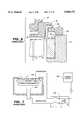
- FIG. 1is a cross-sectional view of a prior-art CVD processing chamber.
- FIG. 2is a cross-sectional view of FIG. 1 taken at 2--2 showing the gas flow distribution across the substrate being processed and the gas flow in the pumping channel.
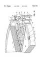
- FIG. 3is an schematical closeup view of the upper right hand comer of the chamber as shown in FIG. 1.
- FIG. 4is a cross-sectional view of an integrated-circuit structure which the apparatus of the invention can be used to make.
- FIG. 5is a copy of FIG. 3 showing a conductive film formed on the upper surfaces of the chamber.
- FIG. 7shows the power splitting energization for prior art TiN chambers.
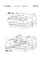
- FIG. 8is a cross-sectional of a processing chamber according to the invention.
- FIG. 9is a schematical cross section of the processing chamber of FIG. 8 showing the interrelationship between the electrical potentials of the structures according to the invention and emphasizing other features.
- FIG. 10is an enlarged view of the upper right hand comer of FIGS. 8 and 9.
- FIG. 11is a perspective cutaway view of the cross section of FIG. 8 showing the interrelationship of various structures of the invention.
- FIG. 12copies FIG. 10 and shows the buildup of a conductive film around a pumping channel liner of the invention.
- FIG. 13copies FIG. 10 and shows the buildup of a conductive film on the novel isolator ring of the invention as would occur from gas traveling from the gas distribution faceplate to the vacuum evacuation system through the pumping channel.
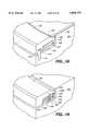
- FIG. 14is a top view of a circular substrate located in a centering ring of a susceptor according to the invention.
- FIG. 15shows a partially sectioned perspective view of a centering boss as part of the centering ring according to the invention.
- FIG. 16shows a closeup plan view of a section of the centering ring with a substrate in position taken at the closeup identified as 16--16 in FIG. 14.
- FIG. 17is similar to FIG. 15 but shows a wafer which has been centered by the boss on the centering ring.
- FIG. 18is a partially sectioned perspective view showing the centering ring, its pin support, and its thermally insulating rings taken at 18--18 in FIG. 14.
- FIG. 19a partially sectioned perspective view of the centering ring (without the substrate present) showing the fastener for the thermally insulating rings taken at 19--19 of FIG. 14.
- FIG. 20is a partially sectioned exploded perspective view of FIG. 14 taken at 20--20 showing the grounding strap of the centering ring with the centering ring shown separated from the pedestal.
- FIG. 21shows a schematic diagram of an RF power supply to generate plasma in the processing chamber according to the invention.
- FIG. 8shows a cross section of a processing chamber according to a first aspect of the invention.
- a pedestal 140supports a wafer 142 on its upper surface 144.
- Gas entering the process gas inlet 44is distributed in the lower manifold 54 and passes into the processing region chamber through the nozzles 42 in the showerhead 40.
- the process gasthen flows as shown in FIG. 2 radially outwardly with respect to a central axis 141, across the edge of the wafer 142, across a peripheral centering ring 146, shown in FIG. 8, disposed in an annular ledge 148 recessed in the upper periphery of the pedestal 140.
- the process gasflows through a choke aperture 150 formed between the bottom of a modified annular isolator 152 and the top of a modified chamber wall insert 154 and into a modified pumping channel 160.
- the chamber wall insert 154is shown to have a sealable passageway 156 through it and through the main chamber body 72 for an unillustrated robot blade to transfer wafers into and out of the reactor.
- the gasonce it enters the pumping channel 160, is routed around the perimeter of the process chamber, similarly to the prior-art pumping channel 60 as shown in FIGS. 1 and 2, to be evacuated by the vacuum pumping system 82 connected to the process chamber.
- FIG. 9The same general chamber is illustrated in FIG. 9 with different aspects of the invention being emphasized.
- the blown up cross section of FIG. 10includes inventive aspects of both FIGS. 8 and 9.
- the generally illustrated chamber insert 154includes an L-shaped insulating ceramic ring 164 resting on the inside ledge 70 of the main chamber body 72 and also includes an annular or band shield 166 resting on an inside ledge 168 of the L-shaped ring 164 and spaced from the pedestal 140 and the centering ring 146 by a small gap.
- Ceramic chamber liners of themselvesare well known, for example, as described by Robertson et al. in U.S. Pat. No. 5,366,585.
- the band shield 166is preferably made of a metal, such as aluminum, and extends vertically upwardly substantially above the top of the L-shaped ceramic ring 164 and to a lesser extent above the supporting surface 144 of the pedestal 140.
- the annular pumping channel 160has sides generally defined by the band shield 166, the L-shaped ring 164, liners 170, 172 placed in front of the main chamber body 72 and the lid rim 66, and the isolator 152, with the choke aperture 150 being formed between the isolator 152 and the band shield 166.
- the lid liner 170is placed on the side of the pumping channel 160 facing the lid rim 66 and conforms to its shape.
- the chamber liner 172is placed on the side of the pumping channel 160 facing the main chamber body 72.
- Both liners 170, 172are preferably made of a metal, such as aluminum, and are bead blasted to increase the adhesion of any film deposited thereon.
- the lid liner 170is detachably fixed to the lid rim 66 by a number of pins 174 and is electrically grounded to the lid rim 66.
- the chamber liner 172is supported on a ledge 176 formed on the outer top of the L-shaped ceramic ring 164 and is precisely formed to have a diameter such that a radial gap 178 is formed between the chamber liner 172 and the main chamber body 72, and an axial gap 180 is formed between the lid and chamber liners 170, 172. That is, the chamber liner 172 is electrically floating.
- the band shield 166 and the lid and chamber liners 170, 172are sized as a set.
- the band shield 166is annular having a major diameter d 1 about the center of pedestal 140.
- the chamber liner 172is also annular and in the shape of a band extending axially along the centerline of the pedestal 140 and with a major diameter d 2 greater than d 1 .
- the lid liner 170is also annular and has an L-shape with the long leg extending radially from d 1 to d 2 and a short leg extending axially at d 2 .
- FIG. 11A partially sectioned, perspective view is given in FIG. 11 of the pedestal 140, centering ring 146, and the liners 170, 172 and shields 152, 166 surrounding the pumping channel 160.
- This figureclearly shows the flow of processing gas out of the nozzles 42 of the showerhead 40 towards the wafer 142 and the subsequent radially outward flow 84 over the wafer 142 and then the centering ring 146. Thereafter, the gas flow is deflected upwardly over the top of the band shield 166 into the pumping channel 160, and in the pumping channel 160 it flows along a circumferential path 86 towards the vacuum pump.
- the pumping channel 160 and its componentsare designed to minimize the effect of any deposited conductive film upon the excitation of a plasma in and near the processing space 56.
- the band shield 166rises above the level of the wafer 142 and of most of the gas flowing over it, a dead space 184 is created in the flow pattern at the bottom of the pumping channel 160 adjacent to a top 186 of the L-shaped ring 164 where it meets the band shield 166.
- the dead space 184ensures that a significant thickness of metal will not deposit around the backside of the band shield 166, and in particular an insufficient amount of metal will deposit to bridge a gap 188 formed between the band shield 166 and the top 186 of the L-shaped insulating ring 164.
- the band shield 166even though conducting, remains electrically floating with respect to the pedestal 140 and the main chamber body 72.
- the band shield 166has rounded ends 167 to reduce the possibility of arcing.
- an extraneous conductive film 120 deposited on the insulating ceramic isolator 152 on surfaces in and near the pumping channel 160has the potential of extending the grounding plane of the lid rim 66 to the area adjacent to the biased showerhead 40 to significantly perturb the plasma electric fields and perhaps even to short the biased showerhead 40 across the isolator 152 to the chamber lid rim 66.
- the L-shaped isolator 152is formed on the outer side of the lower part of its depending inner skirt 203 with two deep annular grooves 205, 207 having widths sufficient to ensure that the deposited film 120 will not bridge the grooves 205, 207.
- the grooves 205, 207are deep enough that a dead space occurs at their bottom so that, even though some deposition is inevitable, it does not form a continuous film on the interior surfaces of the grooves 205, 207.
- the openings of the grooves 205, 207 into the pumping channel 160are generally rounded to prevent arcing from any built up conductive film.
- the grooves 205, 207may have a width of 40 to 80 mils (1-2 mm) and a depth of 100 to 175 mils (2.5-4.6 mm) in the case that the isolator 152 has a width in the skirt 203 of 200 to 400 mils (5-1 mm). With this structure, even if the extraneous film 120, as illustrated in FIG. 13, does deposit on the isolator 152, it does not form a continuous conductive film. Thereby, neither is the showerhead 40 shorted out nor is an extraneous grounding plane established adjacent to the showerhead 40.
- the lid liner 170is metallic and is both thermally and electrically connected to the lid rim 66, effectively forming an extension of it, and because of its remote location does not easily affect the plasma in the processing region 56. Any metal depositing on the lid liner 170 will not further affect the plasma as long as the metal does not extend over the isolator ring 152. In any case, the lid liner 170 is easily removed by means of the fastener 174 when it becomes excessively coated.
- the centering ring 146performs two functions. It acts to precisely center the wafer 142 on the pedestal 140, the wafer 142 having been transferred into the chamber and onto the pedestal 140 by a robot blade moving through the access passageway 156 of FIG. 8. This function blends with a retaining function in which the peripheral ring 146 acts as a retaining ring to hold the wafer 142 within its opening. Additionally, the centering ring 146 acts as a thermal blanket for the portion of the pedestal 140 exposed outside of the wafer 142.
- the centering ring 146thermally floats relative to the heated pedestal 140 and remains relatively cool compared to the wafer 142 and significantly cooler than the underlying pedestal 140, and thus little material is deposited on it during thermal CVD processing.
- the centering ring 146as illustrated in plan view in FIG. 14 and in a sectioned perspective view in FIG. 15, includes a flat annular upper surface 190 and inside and below this surface 190 an annular ledge 192, which is sized so as to closely face the wafer 142 with a thin gap between it and the wafer 142 so as to provide thermal insulation but to nonetheless create a barrier to gas flow.
- the wafer 142 shown in FIG. 14is substantially circular, as is the centering ring 146. However, if the wafer is formed with a large alignment flat on one edge, the inside of the centering ring 146 should be shaped to conform to the flat. As shown in FIG.
- a step wall 194rises from the ledge 192 to the flat upper surface 190 of the centering ring 146.
- the height of the step wall 194equals or is somewhat more than the thickness of the wafer 142 so that the top surface of the wafer 142 supported on or cantilevered slightly above the surface of the ledge 192 is even with the upper surface 190 of the centering ring.
- a series of six centering bosses 200are equally distributed at 60° intervals about the centering ring 146 with respect to a center 201 of the pedestal 140 to which the centering ring 146 is also concentric.
- the centering bosses 200rise from the ledge 192 but only partially protrude from the step wall 194.
- the bossesinclude a cylindrical base 202 and a truncated cone 204 above it, the separation line being somewhat below the planar upper surface 190 of the centering ring so that the truncated cone 204 projects above the planar upper surface 190.
- both the convex and concave comers of the boss 200are smoothed to reduce any arcing or chipping of the wafer.
- Related centering pins though mounted in the pedestalhave been disclosed by Lei et al. in U.S. Pat. No. 5,516,367.
- the centering ring 146is supported on the pedestal 140 by mechanical means to be described later.
- both the pedestal 140 and the lift ring 39 of FIGS. 1 and 8are lowered out of the way.
- the lift ring 39then rises to raise the lift pins 38 out of the pedestal 140 to a sufficient height that their conical heads slightly lift the wafer 142 off the robot blade.
- the robot bladeis then withdrawn, and the pedestal 140 and attached centering ring 146 are raised so that the lift pins 38 supporting the wafer 142 effectively retract toward the supporting surface 144 of the pedestal 140.
- the wafer 142is not precisely centered with respect to the pedestal center 201, as it approaches the pedestal 140 it will first encounter one or two of the centering bosses 200 on their conical tops 204.
- the tapered surfaces of the conical tops 204will exert sufficient lateral force on the wafer 142 that will slide towards the center 201 of the pedestal 140, thus centering the wafer 142.
- the wafer 142upon being further lowered relative to the pedestal 140 will be located, as illustrated in the partially sectioned perspective view of FIG. 17, in a centered position inside the cylindrical bases 202 of all the centering bosses 200.
- the wafer 142is thermally isolated from the centering ring 146 as much as possible. Because the cylindrical bases 202 of the bosses 200 only partially protrude into the area of the ledge 192, a gap 206, shown in FIG. 17, is formed between the beveled edge of the wafer 142 and the step wall 194 of the centering ring. Also, the locus of the extreme radially inward positions of the cylindrical bases 202 of the bosses 200 is sized to be slightly larger than the diameter of the wafer 142, such that a thin gap 208 is designed to exist between the wafer edge and the cylindrical bases 202. However, because of the centering action for a misaligned wafer, the wafer 142 may contact one or two of the centering bosses 200. Nonetheless, any resultant contact is a thin vertical line where the cylindrical wafer 142 contacts the cylindrical boss base 202 so as to minimize conductive heat transfer.
- the wafer 142 during CVD processingis gravitationally supported on the pedestal 140, but the height of the upper surface of the ledge 194 of the centering ring 146 is tightly controlled so that it is slightly below the effective supporting surface 144 of the pedestal 140 and the wafer edge is cantilevered over the upper surface of the ledge 192 with a thin gap between.
- the gap between the wafer edge and the ledge 192is large enough at the operational deposition pressures to provide good thermal isolation, but is small enough and long enough to present sufficient aerodynamic resistance to prevent flow of deposition gas to the backside of the wafer. Also, the gap is thin enough to prevent a plasma from entering the gap and producing arcing.
- the centering ring 146is not only thermally isolated from the wafer 142 but is also thermally isolated from the pedestal 140.
- the centering ringis preferably composed of aluminum or nickel-coated stainless steel. As best shown in the perspective view of FIG. 18, the centering ring 146 is supported above the peripheral ledge 148 of the pedestal 140 by three evenly spaced support pins 210 fixed into the ledge 148 of the pedestal 140 and projecting upwardly therefrom by a precise height.
- the support pins 210effectively present point contacts between the pedestal 140 and the centering ring 146 because of their very small cross section compared to the area of the centering ring 146.
- the support pins 210are preferably made of ceramic or a metal having a low thermal conductivity, such as stainless steel.
- the support pins 210loosely fit into respective radial slots 212 extending from a bottom of an outer annular base 214 of the centering ring 146 and support the centering ring 146 at a precisely set height above the pedestal's ledge 148.
- the radially elongated shape of the slots 212allows for differential thermal expansion between the centering ring 146 and the pedestal 140.
- thermally insulating rings 216, 218Radiative and convective thermal transfer between the bottom of the centering ring 142 and the pedestal is minimized by a stack of thermally insulating rings 216, 218 spaced between a bottom surface of an inwardly projecting rim 220 of the centering ring 146 and the ledge 148 of the pedestal 140.
- the thermally insulating rings 216, 218are preferably formed of ceramic or other material of low thermal conductivity, such as stainless steel, to reduce the conductive transfer of heat therethrough.
- the thermally insulating rings 216, 218are fixed to the bottom of the projecting rim 220 of the centering ring 146 by a series of fasteners 224, such as screws or rivets, arranged on the centering ring 146, as shown in the plan view of FIG. 14.
- the fasteners 224are positioned so that gaps are formed between the pair of rings 216, 218 and both the base 214 of the centering ring 146 and the ledge 148 of the pedestal 140.
- Conical heads 225 of the screw fasteners 224are recessed in counter sinks 226 at the bottom of the bottom ring 218 so as to present a smooth surface.
- the two rings 216, 218are separated from each other and from the projecting rim 220 of the centering ring 146 by either thermally insulating spacers 227 or by spacing bumps 228, shown in FIG. 20, to form a gap 229 between the rings 216, 218 as well as a gap 229A between the rings and the projection 220 of the centering ring 146. These various gaps further cause the rings 216, 218 to thermally float so as to more effectively thermally separate the centering ring 146 from the pedestal 140. Two such rings have been shown to reduce the radiative thermal transfer by 65%; three rings, by 75%.
- the many means used to thermally isolate the centering ring 146also tend to electrically isolate it. As a result, it tends to become electrically charged in the presence of a plasma in the processing space 56. Such electrical charging needs to be avoided because it can produce arcing between the centering ring 146 and the wafer 142, causing direct damage to the wafer. Arcing to any other point produces particles which are apt to settle on the wafer and produce defects. Thus, it is desired that the centering ring 146 and the pedestal 142 be held to the same electrical potential.
- grounding strap 230is composed of a thin tab 232 of an electrically conductive and mechanically soft metal, such as aluminum, which is permanently joined to the base 214 of the centering ring 146 by a weld 234.
- the thickness of the metal tab 232is thin enough so that it conducts little heat and does not mechanically support the centering ring 146.
- the pedestal 140is formed on its periphery with a shallow, axially extending slot 236 with a deeper slot section 238 being formed at its bottom.
- the tab 232is bent at its bottom into a Z-shaped section 240 such that the upper part of the tab 232 fits into the shallow slot 236 and the Z-shaped section 240 fits into the deeper slot section 238.
- a hole 242 formed in the very bottom of the tab 232passes a screw 244, which is then threaded into a corresponding hole in the pedestal 140 within the deeper slot section 238, thus completing the electrical grounding.
- the shallow slot 236encompasses both the tab 232 and the head of the screw 244 so as to maintain a nominal perimeter outline 246 of the pedestal 140.
- the shallow slot 236 and the ground strap 230are configured such that any differential motion due to temperature differences between the pedestal 140 and the centering ring 146 are accommodated without interference between the pieces while electrical continuity is maintained between the centering ring 146 and the pedestal 140.
- FIG. 21shows a configuration according to the present invention of the RF power supply to be compared to that of FIG. 7.
- the pedestal electrode 132is maintained at a ground potential, and only the upper electrode 134 is powered by an RF generator 250 with a fixed matching circuit 252.
- the liners used in the pumping channel and the grounded centering ring of the inventionsufficiently stabilize the plasma 254 that the power splitting between the electrodes 132, 134 as required before is no longer necessary. It is preferred that no bias be applied to the pedestal 132 supporting the electrode since any RF bias tends to electrically charge the wafer and to induce it to discharge to adjacent points, thus causing direct damage or particles.
- the pumping chamber liners and the centering ring of the inventioncan be easily replaced with new or refurbished components whenever films, particularly conductive films, inevitably buildup on them.
- testing in a realistic operating environmenthas shown that even after 3000 wafers, the novel design has minimized the deposition to the point that they do not need to be replaced.
- the inventionis obviously applicable to any process in which the same chamber is used for a thermal metal deposition and another plasma process.
- the titanium layer 106can be deposited by a plasma process using TiCl 4 as the precursor and using the thermal TDMAT process for the TiN layer.
- the processcan be advantageously applied to CVD of conductive metal oxides, such as perovskites including lanthanum oxide.
- the combination of deposition of conductive metals and a plasma stepwould still present the potential problems of a thermal process depositing extraneous metal layers which could affect the plasma process.
- the inventionis of course applicable to many other types of metal CVD processes and should be useful in dielectric CVD and other plasma applications as well.
Landscapes
- Chemical & Material Sciences (AREA)
- Engineering & Computer Science (AREA)
- Chemical Kinetics & Catalysis (AREA)
- General Chemical & Material Sciences (AREA)
- Materials Engineering (AREA)
- Mechanical Engineering (AREA)
- Metallurgy (AREA)
- Organic Chemistry (AREA)
- Plasma & Fusion (AREA)
- Physics & Mathematics (AREA)
- Analytical Chemistry (AREA)
- Chemical Vapour Deposition (AREA)
- Electrodes Of Semiconductors (AREA)
Abstract
Description
This invention relates to semiconductor fabrication equipment. In particular, the invention relates to components used in a plasma reactor for chemical vapor deposition (CVD) pertaining to gas flow through and out of the reactor chamber.
Semiconductor integrated circuits are fabricated with multiple layers, some of them patterned, of semiconductive, insulating, and conductive materials, as well as additional layers providing functions such as bonding, a migration barrier, and an ohmic contacts. Thin films of these various materials are deposited or formed in a number of ways, the most important of which in modern processing are physical vapor deposition (PVD), also known as sputtering, and chemical vapor deposition (CVD).
In CVD, a substrate, for example, a silicon wafer, which may already have patterned layers of silicon or other materials formed thereon, is exposed to a precursor gas which reacts at the surface of the substrate and deposits a product of the reaction on the substrate to thereby grow a film thereon. A simple example includes the use of silane (SiH4) to deposit silicon with the hydrogen forming a gaseous byproduct which is evacuated from the chamber. However, the present application is directed more to CVD of a conductive material such as TiN.
This surface reaction can be activated in at least two different ways. In a thermal process, the substrate is heated to a sufficiently high temperature to provide the activation energy for molecules of the precursor gas adjacent to the substrate to react there and deposit a layer upon the substrate. In a plasma-enhanced CVD process (PECVD), the precursor gas is subjected to a sufficiently high field that it forms a plasma. As a result the precursor gas is excited into energetic states, such as ions or radicals, which readily react on the substrate surface to form the desired layered material.
Zhao et al. describe an example of a CVD deposition chamber in U.S. patent application Ser. No. 08/348,273 filed on Nov. 30, 1994, now issued as U.S. Pat. No. 5,558,717 expressly incorporated herein by reference, and which is assigned to a common assignee. This type of CVD chamber is available from Applied Materials, Inc. of Santa Clara, Calif. as the CVD DxZ chamber.
As described in this patent and as illustrated in the cross sectional side view of FIG. 1, aCVD reactor chamber 30 includes apedestal 32 supporting on a supporting surface 34 awafer 36 to be deposited by CVD with a layer of material.Lift pins 38 are slidable within thepedestal 32 but are kept from falling out by conical heads on their upper ends. The lower ends of thelift pins 38 are engageable with a verticallymovable lifting ring 39 and thus can be lifted above the pedestal'ssurface 34. Thepedestal 32 is also vertically movable, and in cooperation with thelift pins 38 and thelifting ring 39, an unillustrated robot blade transfers a wafer intochamber 30, thelift pins 38 raise thewafer 36 off the robot blade, and then thepedestal 32 rises to raise thewafer 36 off thelift pins 38 and onto its supportingsurface 34.
Thepedestal 32 then further raises thewafer 36 into close opposition to agas distribution faceplate 40, often referred to as a showerhead, which includes a large number ofpassageways 42 for jetting the process gas to theopposed wafer 36. That is, thepassageways 42 guide the process gas into aprocessing space 56 towards thewafer 36. The process gas is injected into thereactor chamber 30 through acentral gas inlet 44 in agasfeed cover plate 46 to a first disk-shaped manifold 48 and from thence throughpassageways 50 in abaffle plate 52 to a second disk-shaped manifold 54 in back of theshowerhead 40.
As indicated by the arrows, the process gas jets from theholes 42 in theshowerhead 40 into theprocessing space 56 between theshowerhead 40 andpedestal 32 so as to react at the surface of the closely spacedwafer 36. Unreacted process gas and reaction byproducts flow radially outwardly to anannular pumping channel 60 surrounding the upper periphery of thepedestal 32. Thepumping channel 60 is generally closed but on the receiving end includes anannular choke aperture 62 between thepumping channel 60 and theprocessing space 56 over thewafer 36. Thechoke aperture 62 is formed between anisolator 64, to be described later, set in alid rim 66 and an insulating annular chamber insert 68 resting on aledge 70 on the inside of themain chamber body 72. Thechoke aperture 62 is formed between the main chamber and a removable lid attached to the chamber so that a fullyannular choke aperture 62 can be achieved. Thechoke aperture 62 has a substantially smaller width than the depth of theprocessing space 56 between theshowerhead 40 and thewafer 36 and is substantially smaller than the minimum lateral dimensions of thecircumferential pumping channel 60, for example by at least a factor of five. The width of thechoke aperture 62 is made small enough and its length long enough so as to create sufficient aerodynamic resistance at the operating pressure and gas flow so that the pressure drop across thechoke aperture 62 is substantially larger than any pressure drops across the radius of thewafer 36 or around the circumference of theannular pumping channel 60. In practice, it is not untypical that thechoke aperture 62 introduces enough aerodynamic impedance that the pressure drop from the middle of thewafer 36 to within thepumping channel 60 is no more than 10% of the circumferential pressure drop within thepumping channel 60.
The pumpingchannel 60 is connected through aconstricted exhaust aperture 74 to a pumpingplenum 76, and avalve 78 gates the exhaust through anexhaust vent 80 to avacuum pump 82. Theconstricted exhaust aperture 74 performs a function similar to that of thechoke aperture 62 in introducing an aerodynamic impedance such that the pressure within thepump channel 60 is substantially constant.
The restricted choke andexhaust apertures circumferential pumping channel 60. The resultant gas distribution flow pattern across thewafer 36 is shown in arrowedlines 84 in FIG. 2. The process gas and its reaction byproducts flow from the center of theshowerhead 40 across thewafer 36 and the periphery of thepedestal 32 alongradial paths 84 and then through thechoke aperture 62 to thepumping channel 60. The gas then flows circumferentially alongpaths 86 in thepumping channel 60 to theexhaust aperture 74 and then through theexhaust plenum 76 and theexhaust vent 80 to thevacuum pump 82. Because of therestrictions radial flow 84 across thewafer 36 is nearly uniform in the azimuthal direction.
As shown in FIGS. 1 and 3 (FIG. 3 being a closeup view of the upper right corner of FIG. 1), theledge 70 in thechamber body 72 supports thechamber shield liner 68, which forms the bottom of thepumping channel 60. Thechamber lid rim 66 forms the top and part of the outside wall of the pumpingchannel 60 along with part of thechamber body 72. The inside upper edge of thepumping channel 60 is formed by theisolator ring 64, which is made of a ceramic or other electrically insulating material which insulates themetallic showerhead 40 from thechamber body 72.
The CVDreactor chamber 30 of FIG.1 can be operated in two modes, thermal and plasma-enhanced. In the thermal mode, anelectrical power source 90 supplies power to aresistive heater 92 at the top of thepedestal 32 to thereby heat thepedestal 32 and thus thewafer 36 to an elevated temperature sufficient to thermally activate the CVD deposition reaction. In the plasma-enhanced mode, an RFelectrical source 94 is passed by aswitch 96 to themetallic showerhead 40, which thus acts as an electrode. Theshowerhead 40 is electrically insulated from thelid rim 66 and themain chamber body 72 by theannular isolator ring 64, typically formed of an electrically non-conductive ceramic. Thepedestal 32 is connected to abiasing element 98 associated with theRF source 94 so that RF power is split between theshowerhead 40 and thepedestal 32. Sufficient voltage and power is applied by theRF source 94 to cause the process gas in theprocessing space 56 between theshowerhead 40 and thepedestal 32 to discharge and to form a plasma.
Only recently has it been attempted to use this general type of CVD reactor to deposit a film of a conductive material, such as titanium nitride (TiN), using the thermal TDMAT process described by Sandhu et al. in U.S. patent application, Ser. No. 07/898,059. A related plasma process is described by Sandhu et al. in U.S. Pat. 5,246,881. The deposition of a conductive material in this chamber has presented some problems that are addressed by this invention.
Titanium nitride is a moderately good electrical conductor, but in semiconductor processing it is used primarily to function as a barrier layer and to assist titanium as a glue layer. This process is often applied to the contact structure illustrated in the cross-sectional view of FIG. 4 in which anoxide layer 100, typically SiO2, is deposited to a thickness of about 1 μm over asubstrate 102 having a surface of crystalline silicon or polysilicon. Theoxide layer 100 acts as an inter-level dielectric, but to provide electrical contact between levels acontact hole 104 is etched through theoxide layer 100 to be filled with a metal such as aluminum. However, in advanced integrated circuits, thecontact hole 104 is narrow, often less than 0.35 μm, and has an aspect ratio of 3 or more. Filling such a hole is difficult, but a somewhat standard process has been developed in which thehole 104 is first conformally coated with atitanium layer 106, and thetitanium layer 106 is then conformally coated with atitanium nitride layer 108. Thereafter, analuminum layer 110 is deposited, usually by physical vapor deposition, to fill thecontact hole 104 and to provide electrical interconnection lines on the upper level. TheTi layer 106 provides a glue layer to both the underlying silicon and the oxide on the sidewalls. Also, it can be silicided with the underlying silicon to form an ohmic contact. TheTiN layer 108 bonds well to theTi layer 106, and thealuminum layer 110 wets well to the TiN so that the aluminum can better fill thecontact hole 104 without forming an included void. Also, theTiN layer 108 acts as a barrier to prevent thealuminum 110 from migrating into thesilicon 102 and affecting its conductivity. In a via structure in which thesubstrate 102 includes an aluminum surface feature, theTi layer 106 may not be needed. Even though the electrical conductivities of titanium and titanium nitride are not nearly as high as that of aluminum, they are sufficiently conductive in thin layers to provide a good electrical contact.
Titanium and titanium nitride can be deposited by either CVD or PVD, but CVD enjoys the advantage of more easily forming conformal layers in a hole having a high aspect ratio. The thermal TDMAT process is such a CVD process for conformally coating TiN in a narrow hole.
In the TDMAT process, a precursor gas of tetrakis-dimethylamido-titanium, Ti(N(CH4)2)4, is injected into the chamber through theshowerhead 40 at a pressure of about 1 to 9Torr while thepedestal 32 holds thesubstrate 36 at an elevated temperature of about 360° C. or higher. Thereby, a conductive and conformal TiN layer is deposited on thesubstrate 36 in a CVD process. The TDMAT process is a thermal process not usually relying upon plasma excitation of the precursor gas.
However, it has been found that the TiN layer initially formed by the TDMAT process includes an excessive amount of carbon in the form of included polymers which degrade its conductivity. Thus, the TDMAT deposition is usually followed by a second step of plasma treating the deposited TiN layer. The TDMAT gas in the chamber is replaced by a gas mixture of H2 and N2 in about a 50:50 ratio at a pressure of 0.5 to 10 Torr, and theRF power source 94 is switched on to create electric fields between theshowerhead 40 and thepedestal 32 sufficient to discharge the H2 :N2 gas to form a plasma. The hydrogen and nitrogen species in the plasma reduce the carbonaceous polymer to volatile byproducts which are exhausted from the system. The plasma treatment thereby removes the carbon to improve the quality of the TiN film.
The plasma treatment process, when performed in the same chamber as the thermal CVD deposition, has demonstrated some problems with uniformity and reproducibility. We believe that the problems originate from extraneous metal depositions on reactor surfaces affecting the plasma and producing excess particles within the chamber. We also believe that the depositions occur in two different areas, an area at the top of thepedestal 32 outside of thewafer 36 and an area in and around the pumpingchannel 60.
A first problem, we believe, relates to extraneous metal deposition on thepedestal 32 because exposed portions of thepedestal 32 are at a temperature equal to and often much greater than that of thewafer 36. As shown in the cross-sectional view of FIG. 3, the portion of thepedestal 32 which extends beyond the outside edge of thewafer 36 is subject to abuildup b 120 of deposited material from the following mechanism.
During the thermal phase of the TDMAT process during which the conductive TiN is deposited, theheater 92, shown in FIG. 1, installed in thepedestal 32 heats thepedestal 32, and the heat is transferred thence to thewafer 36. There are several reasons why the exposed portion of thepedestal 32 tends to be at a significantly higher temperature than that of thewafer 36. Theshowerhead 40 operates at a much lower temperature, typically around 100° C. to readily sink heat from opposed elements. On the other hand, thewafer 36 is incompletely heat sunk on thepedestal 32 and transmits heat conducted to it from thepedestal 32 more poorly than does the directly radiating and more highly thermallyconductive pedestal 32. Also, since the chamber is also used for the low-temperature plasma treating phase and additional time is consumed transferring wafers into and out of the chamber, the duty cycle for the high-temperature operation is relatively low and it is necessary to heat thewafer 36 to the required high processing temperatures. To quickly raise the temperature of thewafer 36 to its processing temperature, the temperature of thepedestal 32 is raised to a higher temperature than that of thewafer 36. For all these reasons, the processing temperature of thewafer 36 may be set to 360° C. while the exposed portion of the pedestal tends to be at a significantly higher temperature of 425°C.
Since the rate of deposition on a surface is proportional to the temperature of the surface (the higher the temperature the more rapid the deposition), the higher temperature of the exposed outer edge of thepedestal 32 causes, as illustrated in FIG. 3, arapid buildup 120 of deposited film. As the thickness of the deposited film increases over the processing cycles of many wafers, deleterious effects may occur. The buildup of film thickness at the edge may create an artificial perimeter rim which prevents thewafer 36 from being in full contact with the surface of thepedestal 32, as required for efficient processing. Similarly, once thebuildup 120 has developed past some film thickness of the film, successively deposited film layers do not completely adhere to the underlying layers. Portions of the film can then form particles or flakes that separate from the pedestal and float onto thewafer 36 being processed. The particles can create defects on the processed wafer.
A second problem related to extraneous metal deposition arises in that the conductive TiN film is also deposited, to a lesser extent because of lower surface temperatures, on other surfaces exposed to the process gas along its path from theshowerhead 40 to and through the pumpingchannel 60 on its way to thechamber vacuum system 82. FIG. 5 shows an example of the buildup of ametal film 124 over and around theisolator ring 64 that can cause an electrical short between the electrically biasedshowerhead 40 and the groundedlid rim 66. FIG. 5 shows only anexaggerated film buildup 124 on the upper surface of the chamber. In reality, the film builds up on all surfaces, but the other buildup is not shown for clarity.
Another example of extraneous film deposition illustrated in FIG. 6 is the buildup of aconductive film 128 over the insulatingalumina chamber insert 68 to the point that it extends across the pumpingchannel 60 and contacts the electrically groundedmain chamber body 72. Thisextraneous deposition 128 thus extends the ground potential associated with thechamber body 72 and thelid rim 66 to the inner, upper edge of the insulatingannular insert 68 closely adjacent the upper peripheral edge of thepedestal 32. The location and quality of plasma in theprocessing space 56 depends on the distance between the powered plasma source electrodes and surrounding surfaces and the difference between their respective electrical potentials. When, during a long process run, thechamber insert 68 effectively changes from being disposed as a insulator between thechamber body 72 and the plasma to being a grounded conductor, the location and quality of the plasma will be affected, particularly around the edges of thesubstrate 36. The distortion of the plasma due to the proximity of a closely adjacent electrical ground causes non-uniformity in the plasma, which affects the thickness of the film deposition and its surface properties.
During plasma processing, variations in uniformity of the plasma will affect the surface uniformity of the film produced. Therefore, variations in the intensity of the plasma will affect the uniformity of film properties. The conductivity, which is the inverse of the insulating quality, of the insulating members surrounding the location of the plasma changes as a conductive film is formed on their surfaces and as the conductive film forms a conductive path to adjacent conductive elements at different potentials. This variation in the conductive quality of the ostensibly insulating elements causes variations in the plasma which reduce the process repeatability.
A third problem related to extraneous metal deposition arises in that some electrically floating elements which are exposed to the plasma will accumulate a charge from the plasma. In the instance where these charged pieces are close to a grounded or electrically powered part, there is always a chance of arcing between the floating part and a ground or the electrode. In the instance when the wafer is supported on the pedestal, the wafer may act as a floating element which can become charged to cause arcing. Arcing creates particles and defects in the substrate. Therefore arcing to the wafer should be avoided and the uniformity of the envelope for the plasma treating the surface of the substrate should be held as uniform as possible.
To avoid these potentially deleterious effects, it is common practice to schedule a cleaning or maintenance cycle involving removal and replacement or cleaning of the pedestal before buildup of film can create undesired effects. However, this remedy is disadvantageous. Not only are pedestals expensive, but their replacement or cleaning involves a shut down of expensive equipment and additional operator time.
The buildup of unwanted film thickness on either the perimeter of the susceptor or across insulating members in the chamber requires they be periodically cleaned to prevent short-circuiting or unacceptable variations in the plasma treatment. The buildup of a thickness of an unwanted film creates a risk of short-circuiting by causing variations in the intensity and location of the electrical fields exciting the gas to a plasma state. Also, when the risk of conduction or arcing becomes high, a cleaning or maintenance cycle is initiated to restore the original distribution of the electrical field. Other consumable or maintainable components also require replacement or cleaning at certain intervals. Presently the risk of conductance and arcing sets the cleaning/maintenance interval. The mean number of wafers between cleans could be increased dramatically if the problem of film thickness adherence and conductivity across insulating members to grounded members, as described above, could be reduced or eliminated.
A CVD chamber, schematically illustrated in FIG. 7, is similar to that of FIG. 1 except that it is radiantly, not resistively, heated. It has been applied to the deposition of conductive materials and where plasma treatment of one sort or another was performed in the chamber. In this chamber, an argon treatment sputtering gas was energized into aplasma 130 between apedestal electrode 132 and acounter electrode 134. AnRF power source 136 provide RF power to energize the plasma. It was found, however, that, if the plasma was to be well confined in the processing space above the wafer, it was necessary to feed the RF power to amatching network 138 that selectably split the power between thepedestal electrode 132 and thecounter electrode 134. It is believed that thus splitting the RF power better confines the plasma because the plasma with a grounded electrode tends to spread outside of the area of the wafer and to be more affected by the extraneously deposited metal layers described above. Thematching network 138 allowed the RF power split to thepedestal electrode 132 to be the fraction of 30%, 50%, or 70% of the total power.
It is desired that CVD chambers of the type shown in FIG. 1, which were designed for deposition of dielectrics, be adapted to allow them to deposit metallic materials.
Therefore, it is desired that this chamber be improved to alleviate the problems of plasma instability and arcing. It is flier desired that the frequency for routine maintenance and cleaning be reduced.
This invention extends the mean number of wafers between cleans by improving the performance of a semiconductor substrate processing chamber, for example, a chamber for depositing titanium nitride.
The performance is improved by reducing the tendency of the deposition gas to form an excessive buildup on the portion of the susceptor extending beyond the edge of the substrate being processed. Reducing the temperature of a peripheral ring surrounding the outer edge of the substrate being processed reduces the buildup.
The invention includes a peripheral ring on the substrate support pedestal which is thermally isolated from the pedestal and the substrate being processed. The peripheral ring includes centering bosses extending above the ring which assist in centering the substrate as it is lowered to the surface of the support pedestal. The centering bosses provide a series of protruding features extending inward from the inside perimeter edge of the ring facing the substrate. These protrusions potentially are the only part of the peripheral ring in contact with the substrate, thereby providing a minimum of surface contact (and potential for conductive heat transfer) between the substrate and the peripheral centering ring.
The peripheral centering ring is thermally isolated from the pedestal by being supported on pins at only three locations around the periphery thereby reducing the conductive heat transfer from the pedestal to the peripheral centering ring. The thermal isolation from the pedestal is further achieved by providing a series of isolator rings or radiation shields (for example, two) which are attached to the bottom side of the peripheral ring. The radiation shields act as barriers to prevent the direct transmission of thermal radiation from the pedestal to the peripheral centering ring. The lower temperature of the peripheral ring as a result of this thermal isolation causes a lower rate of vapor film deposition on its surface and increases the mean number of wafers between cleaning cycles for the processing chamber. The separate peripheral ring can easily be removed and replaced during a maintenance cycle of the processing chamber.
The peripheral ring being thermally isolated from the pedestal is subject to a buildup of static charge which can result in arcing to and from the wafer and/or other adjacent surfaces. The invention includes a grounding strap between the peripheral ring and the pedestal to eliminate arcing between the peripheral ring and the substrate or other adjacent surfaces. The ground strap is flexible and is mounted in a recessed slot on the perimeter of the susceptor such that the ground strap does not provide a protrusion which extends beyond the normal nominal perimeter of the susceptor.
Performance is also improved by reducing and nearly eliminating the likelihood that a continuous conductive film will be formed across insulating elements within the chamber. A continuous choke gap is created in and between adjacent elements having different electrical potentials across which a conductive film might create a change in insulating properties.
An isolating member (ring) in the lid of the processing chamber, includes a series of continuous choke gap surface features (grooves) which prevent the formation of continuous conductive film on the surface of the isolation member. The film formed on the surface is not continuous and therefore does not provide a conductive path from the gas distribution faceplate/electrode to ground. Electrical or charge conduction and/or leakage to ground will eliminate or reduce the electrical field needed to form a uniform plasma and to provide uniform processing of substrates through consecutive processing cycles.
To reduce the possibility of grounding of the metal shield surrounding the plasma region, a (second) continuous choke gap is created around the processing chamber between a second shield element and the chamber body. While the gas is still susceptible to having conductive films being formed therein, the width and depth of the gap prevents the surface film from forming a conductive bridge or connection across the gap or within the gap.
Performance is further improved by providing an electrically floating conductive element surrounding the plasma location to stabilize the edge of the plasma envelope. In one instance a metal shield, which is electrically floating, lines a portion of a wall of the substrate processing chamber. The shield becomes coated during vapor deposition, but process stability is maintained because the shield is electrically isolated from surrounding conductive elements. The shield provides a barrier to passage of the plasma. The static charge on the conductive (metal) shield is uniformly distributed across it and as a result the edge of the plasma envelope is stabilized.
Another improvement involves using RF power provided exclusively to the upper electrode (the gas distribution plate) while the lower electrode (susceptor) is grounded. This 100% to 0% power splitting proves an improvement in the uniform properties of film in a chamber performing a TiN film deposition.
The invention includes a method of isolating a peripheral ring in a susceptor extending beyond the edge of the substrate, including steps of providing a series of support point features from the top of the susceptor and providing a radiation shield ring shielding a portion of the peripheral ring from direct exposure to the susceptor. Another method includes the steps of providing a grounding strap that is electrically connected to the peripheral ring and removably attaching a portion of the grounding strap to the susceptor. Another method of the invention includes the steps of providing an isolator ring exposed at least on one side to the atmosphere of the processing chamber between an RF powered electrode and an electrically conductive element having an electrical potential different from the RF powered electrode, and providing a continuous choke gap in the surface of the isolator member facing the atmosphere of the processing chamber. Another feature of the invention includes a method including the steps of providing a shield supported by an insulating member within the process chamber and providing a clearance between the inner shield member and a grounded surface such that a film forming on the surface will not bridge the gap to provide conductivity.
The invention also includes a method of providing power to a TiN vapor deposition chamber including the steps of connecting an electrode gas distribution plate to a power source and connecting a susceptor opposite the electrode gas distribution plate to the electrode to a ground potential.
This invention provides improvements which reduce the chance of arcing between floating charged elements in the processing chamber adjacent to the location where plasma is formed, reduce the temperature of the peripheral ring to avoid excessive deposition on the part of the susceptor outside the substrate, provides a constant potential across the substrate to eliminate arcing between its peripheral/centering ring and the susceptor and eliminates or substantially reduces the likelihood that any film formed by the vapor deposition on the chamber walls will result in a short circuit connection between the RF electrode and a chamber body or lid. The invention also includes the positioning of a metal (uniform electrical potential distribution ring) around the region of the plasma to contain the plasma and help keep it stable with a relatively constant ion potential across the wafer.
FIG. 1 is a cross-sectional view of a prior-art CVD processing chamber.
FIG. 2 is a cross-sectional view of FIG. 1 taken at 2--2 showing the gas flow distribution across the substrate being processed and the gas flow in the pumping channel.
FIG. 3 is an schematical closeup view of the upper right hand comer of the chamber as shown in FIG. 1.
FIG. 4 is a cross-sectional view of an integrated-circuit structure which the apparatus of the invention can be used to make.
FIG. 5 is a copy of FIG. 3 showing a conductive film formed on the upper surfaces of the chamber.
FIG. 6 is a copy of FIG. 3 showing a film deposited on the pumping channel protruding into the area exposed to plasma in the chambers.
FIG. 7 shows the power splitting energization for prior art TiN chambers.
FIG. 8 is a cross-sectional of a processing chamber according to the invention.
FIG. 9 is a schematical cross section of the processing chamber of FIG. 8 showing the interrelationship between the electrical potentials of the structures according to the invention and emphasizing other features.
FIG. 10 is an enlarged view of the upper right hand comer of FIGS. 8 and 9.
FIG. 11 is a perspective cutaway view of the cross section of FIG. 8 showing the interrelationship of various structures of the invention.
FIG. 12 copies FIG. 10 and shows the buildup of a conductive film around a pumping channel liner of the invention.
FIG. 13 copies FIG. 10 and shows the buildup of a conductive film on the novel isolator ring of the invention as would occur from gas traveling from the gas distribution faceplate to the vacuum evacuation system through the pumping channel.
FIG. 14 is a top view of a circular substrate located in a centering ring of a susceptor according to the invention.
FIG. 15 shows a partially sectioned perspective view of a centering boss as part of the centering ring according to the invention.
FIG. 16 shows a closeup plan view of a section of the centering ring with a substrate in position taken at the closeup identified as 16--16 in FIG. 14.
FIG. 17 is similar to FIG. 15 but shows a wafer which has been centered by the boss on the centering ring.
FIG. 18 is a partially sectioned perspective view showing the centering ring, its pin support, and its thermally insulating rings taken at 18--18 in FIG. 14.
FIG. 19 a partially sectioned perspective view of the centering ring (without the substrate present) showing the fastener for the thermally insulating rings taken at 19--19 of FIG. 14.
FIG. 20 is a partially sectioned exploded perspective view of FIG. 14 taken at 20--20 showing the grounding strap of the centering ring with the centering ring shown separated from the pedestal.
FIG. 21 shows a schematic diagram of an RF power supply to generate plasma in the processing chamber according to the invention.
FIG. 8 shows a cross section of a processing chamber according to a first aspect of the invention. Apedestal 140 supports awafer 142 on itsupper surface 144. Gas entering theprocess gas inlet 44 is distributed in thelower manifold 54 and passes into the processing region chamber through thenozzles 42 in theshowerhead 40. The process gas then flows as shown in FIG. 2 radially outwardly with respect to acentral axis 141, across the edge of thewafer 142, across a peripheral centeringring 146, shown in FIG. 8, disposed in anannular ledge 148 recessed in the upper periphery of thepedestal 140. From thence, the process gas flows through achoke aperture 150 formed between the bottom of a modifiedannular isolator 152 and the top of a modifiedchamber wall insert 154 and into a modifiedpumping channel 160. Thechamber wall insert 154 is shown to have asealable passageway 156 through it and through themain chamber body 72 for an unillustrated robot blade to transfer wafers into and out of the reactor.
The gas, once it enters the pumpingchannel 160, is routed around the perimeter of the process chamber, similarly to the prior-art pumping channel 60 as shown in FIGS. 1 and 2, to be evacuated by thevacuum pumping system 82 connected to the process chamber.
The same general chamber is illustrated in FIG. 9 with different aspects of the invention being emphasized. The blown up cross section of FIG. 10 includes inventive aspects of both FIGS. 8 and 9.
The generally illustratedchamber insert 154 includes an L-shaped insulatingceramic ring 164 resting on theinside ledge 70 of themain chamber body 72 and also includes an annular orband shield 166 resting on aninside ledge 168 of the L-shapedring 164 and spaced from thepedestal 140 and the centeringring 146 by a small gap. Ceramic chamber liners of themselves are well known, for example, as described by Robertson et al. in U.S. Pat. No. 5,366,585. Theband shield 166 is preferably made of a metal, such as aluminum, and extends vertically upwardly substantially above the top of the L-shapedceramic ring 164 and to a lesser extent above the supportingsurface 144 of thepedestal 140.
Theannular pumping channel 160 has sides generally defined by theband shield 166, the L-shapedring 164,liners main chamber body 72 and thelid rim 66, and theisolator 152, with thechoke aperture 150 being formed between the isolator 152 and theband shield 166. However, thelid liner 170 is placed on the side of the pumpingchannel 160 facing thelid rim 66 and conforms to its shape. Thechamber liner 172 is placed on the side of the pumpingchannel 160 facing themain chamber body 72. Bothliners lid liner 170 is detachably fixed to thelid rim 66 by a number ofpins 174 and is electrically grounded to thelid rim 66. However, thechamber liner 172 is supported on aledge 176 formed on the outer top of the L-shapedceramic ring 164 and is precisely formed to have a diameter such that aradial gap 178 is formed between thechamber liner 172 and themain chamber body 72, and anaxial gap 180 is formed between the lid andchamber liners chamber liner 172 is electrically floating.
Theband shield 166 and the lid andchamber liners band shield 166 is annular having a major diameter d1 about the center ofpedestal 140. Thechamber liner 172 is also annular and in the shape of a band extending axially along the centerline of thepedestal 140 and with a major diameter d2 greater than d1. Thelid liner 170 is also annular and has an L-shape with the long leg extending radially from d1 to d2 and a short leg extending axially at d2.
A partially sectioned, perspective view is given in FIG. 11 of thepedestal 140, centeringring 146, and theliners shields channel 160. This figure clearly shows the flow of processing gas out of thenozzles 42 of theshowerhead 40 towards thewafer 142 and the subsequent radially outward flow 84 over thewafer 142 and then the centeringring 146. Thereafter, the gas flow is deflected upwardly over the top of theband shield 166 into the pumpingchannel 160, and in thepumping channel 160 it flows along acircumferential path 86 towards the vacuum pump.
The discussion of the pumping channel will be completed before the centering ring is again discussed.
As most clearly shown in FIG. 10, the pumpingchannel 160 and its components are designed to minimize the effect of any deposited conductive film upon the excitation of a plasma in and near theprocessing space 56.
Since theband shield 166 rises above the level of thewafer 142 and of most of the gas flowing over it, adead space 184 is created in the flow pattern at the bottom of the pumpingchannel 160 adjacent to a top 186 of the L-shapedring 164 where it meets theband shield 166. As a result, even though metal may deposit on the upper portion of theband shield 166, thedead space 184 ensures that a significant thickness of metal will not deposit around the backside of theband shield 166, and in particular an insufficient amount of metal will deposit to bridge agap 188 formed between theband shield 166 and the top 186 of the L-shaped insulatingring 164. As a result, theband shield 166, even though conducting, remains electrically floating with respect to thepedestal 140 and themain chamber body 72. Theband shield 166 has rounded ends 167 to reduce the possibility of arcing.
As is shown in FIG. 12, it is possible for the process gas to flow along apath 181 in thepumping channel 160 through theaxial gap 180 at the top of thechamber liner 172 and then deposit aconductive film 182 in theaxial gap 180 and in theradial gap 178 on the backside of thechamber liner 172. Since bothgaps gap chamber liner 172. Another extraneous film in thepumping channel 160 would be required to bring the ground from themain chamber body 72 close enough to theprocessing space 56 to significantly affect the plasma fields. Very little, if any, gas will progress down to the bottom end of theradial gap 178 where deposition, if it occurs, might create a bridge between thechamber liner 172 and themain chamber body 72. However, because thechamber liner 172 is mounted on anoutside ledge 176 of the insulating L-shapedring 164, a conductive film would have to fill the gap between the L-shapedring 164 and the main thechamber body 72 for the ground of themain chamber body 72 to extend to theband shield 166.
As shown in FIG. 13, an extraneousconductive film 120 deposited on the insulatingceramic isolator 152 on surfaces in and near the pumpingchannel 160 has the potential of extending the grounding plane of thelid rim 66 to the area adjacent to thebiased showerhead 40 to significantly perturb the plasma electric fields and perhaps even to short thebiased showerhead 40 across theisolator 152 to thechamber lid rim 66. However, as shown more clearly in FIG. 10, the L-shapedisolator 152 is formed on the outer side of the lower part of its dependinginner skirt 203 with two deepannular grooves film 120 will not bridge thegrooves grooves grooves grooves channel 160 are generally rounded to prevent arcing from any built up conductive film. As exemplary dimensions, thegrooves isolator 152 has a width in theskirt 203 of 200 to 400 mils (5-1 mm). With this structure, even if theextraneous film 120, as illustrated in FIG. 13, does deposit on theisolator 152, it does not form a continuous conductive film. Thereby, neither is theshowerhead 40 shorted out nor is an extraneous grounding plane established adjacent to theshowerhead 40.
Thelid liner 170, as illustrated in FIG. 10, is metallic and is both thermally and electrically connected to thelid rim 66, effectively forming an extension of it, and because of its remote location does not easily affect the plasma in theprocessing region 56. Any metal depositing on thelid liner 170 will not further affect the plasma as long as the metal does not extend over theisolator ring 152. In any case, thelid liner 170 is easily removed by means of thefastener 174 when it becomes excessively coated.
The discussion will now turn to the centering ring.
The centeringring 146 performs two functions. It acts to precisely center thewafer 142 on thepedestal 140, thewafer 142 having been transferred into the chamber and onto thepedestal 140 by a robot blade moving through theaccess passageway 156 of FIG. 8. This function blends with a retaining function in which theperipheral ring 146 acts as a retaining ring to hold thewafer 142 within its opening. Additionally, the centeringring 146 acts as a thermal blanket for the portion of thepedestal 140 exposed outside of thewafer 142. Specifically, its thermal characteristics are designed in view of the intended process so that the centeringring 146 thermally floats relative to theheated pedestal 140 and remains relatively cool compared to thewafer 142 and significantly cooler than theunderlying pedestal 140, and thus little material is deposited on it during thermal CVD processing.
The centering function and the structure used to achieve it will be explained first.
The centeringring 146, as illustrated in plan view in FIG. 14 and in a sectioned perspective view in FIG. 15, includes a flat annularupper surface 190 and inside and below thissurface 190 anannular ledge 192, which is sized so as to closely face thewafer 142 with a thin gap between it and thewafer 142 so as to provide thermal insulation but to nonetheless create a barrier to gas flow. Thewafer 142 shown in FIG. 14 is substantially circular, as is the centeringring 146. However, if the wafer is formed with a large alignment flat on one edge, the inside of the centeringring 146 should be shaped to conform to the flat. As shown in FIG. 15, astep wall 194 rises from theledge 192 to the flatupper surface 190 of the centeringring 146. The height of thestep wall 194 equals or is somewhat more than the thickness of thewafer 142 so that the top surface of thewafer 142 supported on or cantilevered slightly above the surface of theledge 192 is even with theupper surface 190 of the centering ring.
A series of six centeringbosses 200, also shown in expanded plan view of FIG. 16, are equally distributed at 60° intervals about the centeringring 146 with respect to acenter 201 of thepedestal 140 to which the centeringring 146 is also concentric. The centeringbosses 200 rise from theledge 192 but only partially protrude from thestep wall 194. The bosses include acylindrical base 202 and atruncated cone 204 above it, the separation line being somewhat below the planarupper surface 190 of the centering ring so that thetruncated cone 204 projects above the planarupper surface 190. Even though the centering boss is defined in these simple geometric terms, both the convex and concave comers of theboss 200 are smoothed to reduce any arcing or chipping of the wafer. Related centering pins though mounted in the pedestal have been disclosed by Lei et al. in U.S. Pat. No. 5,516,367.
The centeringring 146 is supported on thepedestal 140 by mechanical means to be described later. When the robot blade transfers awafer 142 into the chamber, both thepedestal 140 and thelift ring 39 of FIGS. 1 and 8 are lowered out of the way. Thelift ring 39 then rises to raise the lift pins 38 out of thepedestal 140 to a sufficient height that their conical heads slightly lift thewafer 142 off the robot blade. The robot blade is then withdrawn, and thepedestal 140 and attached centeringring 146 are raised so that the lift pins 38 supporting thewafer 142 effectively retract toward the supportingsurface 144 of thepedestal 140.
However, if thewafer 142 is not precisely centered with respect to thepedestal center 201, as it approaches thepedestal 140 it will first encounter one or two of the centeringbosses 200 on their conical tops 204. The tapered surfaces of the conical tops 204 will exert sufficient lateral force on thewafer 142 that will slide towards thecenter 201 of thepedestal 140, thus centering thewafer 142. Thewafer 142, upon being further lowered relative to thepedestal 140 will be located, as illustrated in the partially sectioned perspective view of FIG. 17, in a centered position inside thecylindrical bases 202 of all the centeringbosses 200.
Thewafer 142 is thermally isolated from the centeringring 146 as much as possible. Because thecylindrical bases 202 of thebosses 200 only partially protrude into the area of theledge 192, agap 206, shown in FIG. 17, is formed between the beveled edge of thewafer 142 and thestep wall 194 of the centering ring. Also, the locus of the extreme radially inward positions of thecylindrical bases 202 of thebosses 200 is sized to be slightly larger than the diameter of thewafer 142, such that athin gap 208 is designed to exist between the wafer edge and thecylindrical bases 202. However, because of the centering action for a misaligned wafer, thewafer 142 may contact one or two of the centeringbosses 200. Nonetheless, any resultant contact is a thin vertical line where thecylindrical wafer 142 contacts thecylindrical boss base 202 so as to minimize conductive heat transfer.
Thewafer 142 during CVD processing is gravitationally supported on thepedestal 140, but the height of the upper surface of theledge 194 of the centeringring 146 is tightly controlled so that it is slightly below the effective supportingsurface 144 of thepedestal 140 and the wafer edge is cantilevered over the upper surface of theledge 192 with a thin gap between. The gap between the wafer edge and theledge 192 is large enough at the operational deposition pressures to provide good thermal isolation, but is small enough and long enough to present sufficient aerodynamic resistance to prevent flow of deposition gas to the backside of the wafer. Also, the gap is thin enough to prevent a plasma from entering the gap and producing arcing.
As a result of the following structure, the centeringring 146 is not only thermally isolated from thewafer 142 but is also thermally isolated from thepedestal 140.
Thermal isolation of the centeringring 146 from thepedestal 140 is achieved in two ways. The centering ring is preferably composed of aluminum or nickel-coated stainless steel. As best shown in the perspective view of FIG. 18, the centeringring 146 is supported above theperipheral ledge 148 of thepedestal 140 by three evenly spaced support pins 210 fixed into theledge 148 of thepedestal 140 and projecting upwardly therefrom by a precise height. The support pins 210 effectively present point contacts between thepedestal 140 and the centeringring 146 because of their very small cross section compared to the area of the centeringring 146. The support pins 210 are preferably made of ceramic or a metal having a low thermal conductivity, such as stainless steel. Both the small size of thesupport pines 210 and their low thermal conductivity minimize the conduction of heat between thepedestal 140 and the centeringring 146. The support pins 210 loosely fit into respectiveradial slots 212 extending from a bottom of an outerannular base 214 of the centeringring 146 and support the centeringring 146 at a precisely set height above the pedestal'sledge 148. The radially elongated shape of theslots 212 allows for differential thermal expansion between the centeringring 146 and thepedestal 140.
Radiative and convective thermal transfer between the bottom of the centeringring 142 and the pedestal is minimized by a stack of thermally insulatingrings rim 220 of the centeringring 146 and theledge 148 of thepedestal 140. The thermally insulatingrings
As illustrated in the cutaway perspective view of FIG. 19, the thermally insulatingrings rim 220 of the centeringring 146 by a series offasteners 224, such as screws or rivets, arranged on the centeringring 146, as shown in the plan view of FIG. 14. Thefasteners 224 are positioned so that gaps are formed between the pair ofrings base 214 of the centeringring 146 and theledge 148 of thepedestal 140. Conical heads 225 of thescrew fasteners 224 are recessed in counter sinks 226 at the bottom of thebottom ring 218 so as to present a smooth surface. The tworings rim 220 of the centeringring 146 by either thermally insulatingspacers 227 or by spacingbumps 228, shown in FIG. 20, to form agap 229 between therings gap 229A between the rings and theprojection 220 of the centeringring 146. These various gaps further cause therings ring 146 from thepedestal 140. Two such rings have been shown to reduce the radiative thermal transfer by 65%; three rings, by 75%.
These different thermal isolation means have been tested in a prototype reactor during normal CVD processing of the type described before. In these tests, the temperature of thepedestal 140 was measured to be 430° C., the temperature of thewafer 142 to be 360° C., but the temperature of the centeringring 146 to be only 290° C. At 360° C., satisfactory thermal deposition of TiN is achieved on thewafer 142, but at 290° C. little or none of the same material deposits on the centeringring 146. These temperature differentials are driven by ashowerhead 40 that remains at about 100° C. as well as by other thermal leakages to the side.
The many means used to thermally isolate the centeringring 146 also tend to electrically isolate it. As a result, it tends to become electrically charged in the presence of a plasma in theprocessing space 56. Such electrical charging needs to be avoided because it can produce arcing between the centeringring 146 and thewafer 142, causing direct damage to the wafer. Arcing to any other point produces particles which are apt to settle on the wafer and produce defects. Thus, it is desired that the centeringring 146 and thepedestal 142 be held to the same electrical potential.
One structure to fix the potential of the centeringring 146 to that ofpedestal 140 is a thin, solid,flexible grounding strap 230 illustrated in the cutaway perspective view of FIG. 20. The groundingstrap 230 is composed of athin tab 232 of an electrically conductive and mechanically soft metal, such as aluminum, which is permanently joined to thebase 214 of the centeringring 146 by aweld 234. The thickness of themetal tab 232 is thin enough so that it conducts little heat and does not mechanically support the centeringring 146.
Thepedestal 140 is formed on its periphery with a shallow, axially extendingslot 236 with adeeper slot section 238 being formed at its bottom. Thetab 232 is bent at its bottom into a Z-shapedsection 240 such that the upper part of thetab 232 fits into theshallow slot 236 and the Z-shapedsection 240 fits into thedeeper slot section 238. Ahole 242 formed in the very bottom of thetab 232 passes ascrew 244, which is then threaded into a corresponding hole in thepedestal 140 within thedeeper slot section 238, thus completing the electrical grounding. Theshallow slot 236 encompasses both thetab 232 and the head of thescrew 244 so as to maintain anominal perimeter outline 246 of thepedestal 140. Also, theshallow slot 236 and theground strap 230 are configured such that any differential motion due to temperature differences between thepedestal 140 and the centeringring 146 are accommodated without interference between the pieces while electrical continuity is maintained between the centeringring 146 and thepedestal 140.
FIG. 21 shows a configuration according to the present invention of the RF power supply to be compared to that of FIG. 7. Here, there is no power splitting during the plasma treatment used in conjunction with the thermal TDMAT deposition of TiN. Instead, thepedestal electrode 132 is maintained at a ground potential, and only theupper electrode 134 is powered by anRF generator 250 with afixed matching circuit 252. The liners used in the pumping channel and the grounded centering ring of the invention sufficiently stabilize theplasma 254 that the power splitting between theelectrodes pedestal 132 supporting the electrode since any RF bias tends to electrically charge the wafer and to induce it to discharge to adjacent points, thus causing direct damage or particles.
The pumping chamber liners and the centering ring of the invention can be easily replaced with new or refurbished components whenever films, particularly conductive films, inevitably buildup on them. However, testing in a realistic operating environment has shown that even after 3000 wafers, the novel design has minimized the deposition to the point that they do not need to be replaced. Thus, some relatively simple improvements to the equipment peripheral to the pedestal, all within the confines of the existing chamber of FIG. 1, substantially reduce downtime of the CVD system while providing superior plasma conditions.
Although the invention been described with respect to a thermal CVD of TiN followed by a plasma treatment, the invention is obviously applicable to any process in which the same chamber is used for a thermal metal deposition and another plasma process. For example, thetitanium layer 106 can be deposited by a plasma process using TiCl4 as the precursor and using the thermal TDMAT process for the TiN layer. Also, the process can be advantageously applied to CVD of conductive metal oxides, such as perovskites including lanthanum oxide. The combination of deposition of conductive metals and a plasma step would still present the potential problems of a thermal process depositing extraneous metal layers which could affect the plasma process. The invention is of course applicable to many other types of metal CVD processes and should be useful in dielectric CVD and other plasma applications as well.
While the invention has been described to specific embodiments, those skilled in the art will recognize that changes can be made in form and detail without departing from the sphere and scope of the invention.
Claims (22)
1. A substrate processing reactor, comprising:
a reaction chamber including therein a pedestal for supporting on a generally planar surface thereof a substrate to be processed;
a source of gas disposed over said pedestal;
an exhaust vent disposed around said pedestal on sides of said chamber; and
a peripheral member supported on said pedestal on a side thereof including said planar surface, separated from said pedestal by a space, and thermally floating from said pedestal.
2. The reactor of claim 1, wherein said peripheral member is supported on said pedestal by a number of point contacts.
3. The reactor of claim 2, wherein said number is three.
4. The reactor of claim 2, wherein said point contacts comprise pins fixed in said pedestal and floatingly supporting said peripheral member.
5. The reactor claim 4, wherein said pins provide point contacts between said pedestal and said peripheral member.
6. The reactor of claim 4, wherein said pins comprise a ceramic.
7. The reactor of claim 4, wherein said pins comprise a stainless steel.
8. The reactor of claim 1, wherein said peripheral member is supported in a peripheral recess in said pedestal.
9. The reactor of claim 1, further comprising at least one insulating member disposed between said peripheral member and said pedestal and having respective gaps formed between said insulating member and said peripheral member and between said insulating member and said pedestal.
10. The reactor of claim 9, comprising at least two of said insulating members having gaps formed between them and between a topmost of them and said peripheral.
11. The reactor of claim 1, wherein said peripheral member includes centering bosses for centering said substrate on said pedestal.
12. A substrate processing reactor, comprising:
a reaction chamber including therein a pedestal for supporting on a generally planar surface thereof a substrate to be processed and additionally including pins fixed to said pedestal;
a source of gas disposed over said pedestal;
an exhaust vent disposed around said pedestal on sides of said chamber; and
a peripheral member supported on said pedestal, thermally floating from said pedestal peripheral member, and including radial grooves formed on a bottom thereof for loosely fittingly receiving said pins.
13. A substrate processing reactor, comprising:
a reaction chamber including therein a pedestal for supporting a substrate to be processed;
a source of gas disposed over said pedestal;
an exhaust vent disposed around said pedestal on sides of said chamber;
a peripheral member supported on said pedestal and thermally floating from said pedestal; and
an electrical connector between said peripheral member and said pedestal.
14. The reactor of claim 13, wherein said electrical connector does not significantly support said peripheral member on said pedestal.
15. The reactor of claim 14, further comprising a fastener detachably connecting a bottom of said electrical connector to said pedestal.
16. The reactor of claim 15, wherein said fastener is disposed in an axial groove in said pedestal so as to maintain a nominal perimeter outline of said pedestal.
17. The reactor of claim 13, wherein said pedestal on a substantially planar surface thereof supports said substrate.
18. The reactor of claim 17, wherein said peripheral member is supported on said pedestal on a side thereof including said planar surface.
19. A substrate processing reactor, comprising:
a reaction chamber including an inlet and an outlet for a processing gas;
a pedestal disposed in said chamber for supporting on a top thereof a substrate to be processed, said pedestal including a peripheral recess;
a peripheral member; and
support pins supported on said pedestal and supporting said peripheral member in said recess;
wherein said supported peripheral member has a top surface that is substantially even with a top of said substrate supported on said pedestal.
20. The substrate processing reactor of claim 19, wherein said support pins provide a three-point support for said peripheral member.
21. The substrate processing reactor of claim 19, wherein said peripheral member
a radially inwardly extending ledge above which said supported substrate is disposed; and
a plurality of centering bosses extending over said ledge for centering said substrate on said pedestal.
22. The substrate processing reactor of claim 19, further comprising at least one insulating annular member fixed to a bottom of said peripheral member and having a gap formed between said insulating member and said peripheral member.
Priority Applications (11)
| Application Number | Priority Date | Filing Date | Title |
|---|---|---|---|
| US08/680,724US5846332A (en) | 1996-07-12 | 1996-07-12 | Thermally floating pedestal collar in a chemical vapor deposition chamber |
| US08/857,847US5964947A (en) | 1996-07-12 | 1997-05-16 | Removable pumping channel liners within a chemical vapor deposition chamber |
| TW086108109ATW359853B (en) | 1996-07-12 | 1997-06-12 | Components peripheral to the pedestal in the gas flow path within a chemical vapor deposition chamber |
| KR1019970032160AKR100522903B1 (en) | 1996-07-12 | 1997-07-11 | Components peripheral to the pedestal in the gas flow path within a chemical vapor deposition chamber |
| DE69710961TDE69710961T2 (en) | 1996-07-12 | 1997-07-11 | Components peripheral to the base by gas flow within a chamber for chemical vapor deposition |
| EP97305148AEP0818558B1 (en) | 1996-07-12 | 1997-07-11 | Components peripheral to the pedestal in the gas flow path within a chemical vapor deposition chamber |
| EP01118816AEP1172458A3 (en) | 1996-07-12 | 1997-07-11 | Components peripheral to the pedestal in the gas flow path within a chemical vapor deposition chamber |
| JP9188357AJPH1070088A (en) | 1996-07-12 | 1997-07-14 | Components around pedestal in gas flow path in chemical vapor deposition chamber |
| US08/936,285US5993916A (en) | 1996-07-12 | 1997-09-22 | Method for substrate processing with improved throughput and yield |
| US09/049,856US6270859B2 (en) | 1996-07-12 | 1998-03-27 | Plasma treatment of titanium nitride formed by chemical vapor deposition |
| US09/409,477US6129044A (en) | 1996-07-12 | 1999-10-06 | Apparatus for substrate processing with improved throughput and yield |
Applications Claiming Priority (1)
| Application Number | Priority Date | Filing Date | Title |
|---|---|---|---|
| US08/680,724US5846332A (en) | 1996-07-12 | 1996-07-12 | Thermally floating pedestal collar in a chemical vapor deposition chamber |
Related Child Applications (3)
| Application Number | Title | Priority Date | Filing Date |
|---|---|---|---|
| US08/857,847DivisionUS5964947A (en) | 1996-07-12 | 1997-05-16 | Removable pumping channel liners within a chemical vapor deposition chamber |
| US08/936,285Continuation-In-PartUS5993916A (en) | 1996-07-12 | 1997-09-22 | Method for substrate processing with improved throughput and yield |
| US09/049,856DivisionUS6270859B2 (en) | 1996-07-12 | 1998-03-27 | Plasma treatment of titanium nitride formed by chemical vapor deposition |
Publications (1)
| Publication Number | Publication Date |
|---|---|
| US5846332Atrue US5846332A (en) | 1998-12-08 |
Family
ID=24732256
Family Applications (3)
| Application Number | Title | Priority Date | Filing Date |
|---|---|---|---|
| US08/680,724Expired - LifetimeUS5846332A (en) | 1996-07-12 | 1996-07-12 | Thermally floating pedestal collar in a chemical vapor deposition chamber |
| US08/857,847Expired - LifetimeUS5964947A (en) | 1996-07-12 | 1997-05-16 | Removable pumping channel liners within a chemical vapor deposition chamber |
| US09/049,856Expired - LifetimeUS6270859B2 (en) | 1996-07-12 | 1998-03-27 | Plasma treatment of titanium nitride formed by chemical vapor deposition |
Family Applications After (2)
| Application Number | Title | Priority Date | Filing Date |
|---|---|---|---|
| US08/857,847Expired - LifetimeUS5964947A (en) | 1996-07-12 | 1997-05-16 | Removable pumping channel liners within a chemical vapor deposition chamber |
| US09/049,856Expired - LifetimeUS6270859B2 (en) | 1996-07-12 | 1998-03-27 | Plasma treatment of titanium nitride formed by chemical vapor deposition |
Country Status (6)
| Country | Link |
|---|---|
| US (3) | US5846332A (en) |
| EP (2) | EP1172458A3 (en) |
| JP (1) | JPH1070088A (en) |
| KR (1) | KR100522903B1 (en) |
| DE (1) | DE69710961T2 (en) |
| TW (1) | TW359853B (en) |
Cited By (602)
| Publication number | Priority date | Publication date | Assignee | Title |
|---|---|---|---|---|
| WO1999053116A1 (en)* | 1998-04-09 | 1999-10-21 | Tokyo Electron Arizona, Inc. | Stacked showerhead assembly for delivering gases and rf power to a reaction chamber |
| US6050216A (en)* | 1998-08-21 | 2000-04-18 | M.E.C. Technology, Inc. | Showerhead electrode for plasma processing |
| US6050506A (en)* | 1998-02-13 | 2000-04-18 | Applied Materials, Inc. | Pattern of apertures in a showerhead for chemical vapor deposition |
| US6055927A (en)* | 1997-01-14 | 2000-05-02 | Applied Komatsu Technology, Inc. | Apparatus and method for white powder reduction in silicon nitride deposition using remote plasma source cleaning technology |
| US6063441A (en)* | 1997-12-02 | 2000-05-16 | Applied Materials, Inc. | Processing chamber and method for confining plasma |
| US6092486A (en)* | 1996-05-27 | 2000-07-25 | Sumimoto Metal Indsutries, Ltd. | Plasma processing apparatus and plasma processing method |
| US6106625A (en)* | 1997-12-02 | 2000-08-22 | Applied Materials, Inc. | Reactor useful for chemical vapor deposition of titanium nitride |
| US6129044A (en)* | 1996-07-12 | 2000-10-10 | Applied Materials, Inc. | Apparatus for substrate processing with improved throughput and yield |
| US6170432B1 (en) | 2000-01-24 | 2001-01-09 | M.E.C. Technology, Inc. | Showerhead electrode assembly for plasma processing |
| US6189482B1 (en)* | 1997-02-12 | 2001-02-20 | Applied Materials, Inc. | High temperature, high flow rate chemical vapor deposition apparatus and related methods |
| US6192827B1 (en)* | 1998-07-03 | 2001-02-27 | Applied Materials, Inc. | Double slit-valve doors for plasma processing |
| US6237528B1 (en) | 2000-01-24 | 2001-05-29 | M.E.C. Technology, Inc. | Showerhead electrode assembly for plasma processing |
| US6364954B2 (en)* | 1998-12-14 | 2002-04-02 | Applied Materials, Inc. | High temperature chemical vapor deposition chamber |
| US20020038688A1 (en)* | 2000-08-11 | 2002-04-04 | Alps Electric Co., Ltd. And Tadahiro Ohmi | Plasma processing apparatus and system, performance validation system and inspection method therefor |
| US6368450B2 (en)* | 1997-05-20 | 2002-04-09 | Tokyo Electron Limited | Processing apparatus |
| US6375748B1 (en)* | 1999-09-01 | 2002-04-23 | Applied Materials, Inc. | Method and apparatus for preventing edge deposition |
| US20020060363A1 (en)* | 1997-05-14 | 2002-05-23 | Applied Materials, Inc. | Reliability barrier integration for Cu application |
| US6402847B1 (en) | 1998-11-27 | 2002-06-11 | Kabushiki Kaisha Toshiba | Dry processing apparatus and dry processing method |
| US20020127508A1 (en)* | 2000-07-21 | 2002-09-12 | Applied Materials, Inc. | Emissivity-change-free pumping plate kit in a single wafer chamber |
| US6466881B1 (en)* | 1999-04-22 | 2002-10-15 | Applied Materials Inc. | Method for monitoring the quality of a protective coating in a reactor chamber |
| US6477980B1 (en)* | 2000-01-20 | 2002-11-12 | Applied Materials, Inc. | Flexibly suspended gas distribution manifold for plasma chamber |
| US6485605B1 (en)* | 2000-04-20 | 2002-11-26 | Taiwan Semiconductor Manufacturing Co., Ltd | High temperature process chamber having improved heat endurance |
| US6498091B1 (en) | 2000-11-01 | 2002-12-24 | Applied Materials, Inc. | Method of using a barrier sputter reactor to remove an underlying barrier layer |
| US6499425B1 (en)* | 1999-01-22 | 2002-12-31 | Micron Technology, Inc. | Quasi-remote plasma processing method and apparatus |
| US6559061B2 (en) | 1998-07-31 | 2003-05-06 | Applied Materials, Inc. | Method and apparatus for forming improved metal interconnects |
| US20030087488A1 (en)* | 2001-11-07 | 2003-05-08 | Tokyo Electron Limited | Inductively coupled plasma source for improved process uniformity |
| US6562715B1 (en) | 2000-08-09 | 2003-05-13 | Applied Materials, Inc. | Barrier layer structure for copper metallization and method of forming the structure |
| US20030091753A1 (en)* | 2001-10-25 | 2003-05-15 | Han Jae-Jong | Plasma enhanced chemical vapor deposition apparatus and method for forming nitride layer using the same |
| US6582522B2 (en)* | 2000-07-21 | 2003-06-24 | Applied Materials, Inc. | Emissivity-change-free pumping plate kit in a single wafer chamber |
| US6589352B1 (en)* | 1999-12-10 | 2003-07-08 | Applied Materials, Inc. | Self aligning non contact shadow ring process kit |
| US6656831B1 (en) | 2000-01-26 | 2003-12-02 | Applied Materials, Inc. | Plasma-enhanced chemical vapor deposition of a metal nitride layer |
| US6719499B1 (en)* | 1999-01-13 | 2004-04-13 | Asm International N.V. | Device for positioning a wafer |
| US20040089235A1 (en)* | 2001-12-03 | 2004-05-13 | Takakazu Yamada | Mixer, and device and method for manufacturing thin-film |
| US20040094402A1 (en)* | 2002-08-01 | 2004-05-20 | Applied Materials, Inc. | Self-ionized and capacitively-coupled plasma for sputtering and resputtering |
| US6772827B2 (en) | 2000-01-20 | 2004-08-10 | Applied Materials, Inc. | Suspended gas distribution manifold for plasma chamber |
| US20040167494A1 (en)* | 2001-07-31 | 2004-08-26 | Toshifumi Otsubo | Pants-type disposable wearing article |
| US20040168642A1 (en)* | 1999-12-22 | 2004-09-02 | Kentaro Asakura | Film deposition system |
| US20040237891A1 (en)* | 2003-06-02 | 2004-12-02 | David Stacey | Lid liner for chemical vapor deposition chamber |
| US20050006222A1 (en)* | 1999-10-08 | 2005-01-13 | Peijun Ding | Self-ionized and inductively-coupled plasma for sputtering and resputtering |
| US20050079729A1 (en)* | 2003-10-08 | 2005-04-14 | Woo-Sung Jang | High density plasma oxide film deposition apparatus having a guide ring and a semiconductor device manufacturing method using the same |
| US20050183827A1 (en)* | 2004-02-24 | 2005-08-25 | Applied Materials, Inc. | Showerhead mounting to accommodate thermal expansion |
| US20050259716A1 (en)* | 2002-04-15 | 2005-11-24 | Masafumi Ito | Method and apparatus for measuring temperature of substrate |
| US20050269031A1 (en)* | 2002-04-19 | 2005-12-08 | Nordson Corporation | Plasma treatment system |
| US20060130971A1 (en)* | 2004-12-21 | 2006-06-22 | Applied Materials, Inc. | Apparatus for generating plasma by RF power |
| US20070044714A1 (en)* | 2005-08-31 | 2007-03-01 | Applied Materials, Inc. | Method and apparatus for maintaining a cross sectional shape of a diffuser during processing |
| US20080099146A1 (en)* | 2006-10-25 | 2008-05-01 | Applied Materials, Inc. | Suspension for showerhead in process chamber |
| US20080099145A1 (en)* | 2005-09-02 | 2008-05-01 | Applied Materials, Inc. | Gas sealing skirt for suspended showerhead in process chamber |
| US7402210B2 (en) | 2002-11-14 | 2008-07-22 | Applied Materials, Inc. | Apparatus and method for hybrid chemical processing |
| US20080187682A1 (en)* | 2006-12-20 | 2008-08-07 | Beom Soo Park | Prevention of film deposition on pecvd process chamber wall |
| US7429361B2 (en) | 2002-07-17 | 2008-09-30 | Applied Materials, Inc. | Method and apparatus for providing precursor gas to a processing chamber |
| US7429410B2 (en) | 2004-09-20 | 2008-09-30 | Applied Materials, Inc. | Diffuser gravity support |
| US7494908B2 (en) | 2001-09-26 | 2009-02-24 | Applied Materials, Inc. | Apparatus for integration of barrier layer and seed layer |
| US7514358B2 (en) | 2002-03-04 | 2009-04-07 | Applied Materials, Inc. | Sequential deposition of tantalum nitride using a tantalum-containing precursor and a nitrogen-containing precursor |
| US20090314208A1 (en)* | 2008-06-24 | 2009-12-24 | Applied Materials, Inc. | Pedestal heater for low temperature pecvd application |
| US7682946B2 (en) | 2005-11-04 | 2010-03-23 | Applied Materials, Inc. | Apparatus and process for plasma-enhanced atomic layer deposition |
| US7767024B2 (en) | 2004-02-26 | 2010-08-03 | Appplied Materials, Inc. | Method for front end of line fabrication |
| US7775508B2 (en) | 2006-10-31 | 2010-08-17 | Applied Materials, Inc. | Ampoule for liquid draw and vapor draw with a continuous level sensor |
| US7780793B2 (en) | 2004-02-26 | 2010-08-24 | Applied Materials, Inc. | Passivation layer formation by plasma clean process to reduce native oxide growth |
| US7780788B2 (en) | 2001-10-26 | 2010-08-24 | Applied Materials, Inc. | Gas delivery apparatus for atomic layer deposition |
| US7794544B2 (en) | 2004-05-12 | 2010-09-14 | Applied Materials, Inc. | Control of gas flow and delivery to suppress the formation of particles in an MOCVD/ALD system |
| US7798096B2 (en) | 2006-05-05 | 2010-09-21 | Applied Materials, Inc. | Plasma, UV and ion/neutral assisted ALD or CVD in a batch tool |
| US8074599B2 (en) | 2004-05-12 | 2011-12-13 | Applied Materials, Inc. | Plasma uniformity control by gas diffuser curvature |
| US8083853B2 (en) | 2004-05-12 | 2011-12-27 | Applied Materials, Inc. | Plasma uniformity control by gas diffuser hole design |
| US20120006488A1 (en)* | 2005-09-02 | 2012-01-12 | Tokyo Electron Limited | Ring-shaped component for use in a plasma processing, plasma processing apparatus and outer ring-shaped member |
| US8146896B2 (en) | 2008-10-31 | 2012-04-03 | Applied Materials, Inc. | Chemical precursor ampoule for vapor deposition processes |
| WO2011143062A3 (en)* | 2010-05-12 | 2012-05-10 | Applied Materials, Inc. | Confined process volume pecvd chamber |
| US20120146191A1 (en)* | 2009-08-31 | 2012-06-14 | Showa Denko K.K. | Apparatus and method for manufacturing compound semiconductor, and compound semiconductor manufactured thereby |
| US8328939B2 (en) | 2004-05-12 | 2012-12-11 | Applied Materials, Inc. | Diffuser plate with slit valve compensation |
| US8679982B2 (en) | 2011-08-26 | 2014-03-25 | Applied Materials, Inc. | Selective suppression of dry-etch rate of materials containing both silicon and oxygen |
| US8679983B2 (en) | 2011-09-01 | 2014-03-25 | Applied Materials, Inc. | Selective suppression of dry-etch rate of materials containing both silicon and nitrogen |
| US20140123900A1 (en)* | 2012-11-02 | 2014-05-08 | Industrial Technology Research Institute | Gas shower device having gas curtain and apparatus for depositing film using the same |
| US8765574B2 (en) | 2012-11-09 | 2014-07-01 | Applied Materials, Inc. | Dry etch process |
| US8771539B2 (en) | 2011-02-22 | 2014-07-08 | Applied Materials, Inc. | Remotely-excited fluorine and water vapor etch |
| US8801952B1 (en) | 2013-03-07 | 2014-08-12 | Applied Materials, Inc. | Conformal oxide dry etch |
| US8808563B2 (en) | 2011-10-07 | 2014-08-19 | Applied Materials, Inc. | Selective etch of silicon by way of metastable hydrogen termination |
| US8821637B2 (en) | 2007-01-29 | 2014-09-02 | Applied Materials, Inc. | Temperature controlled lid assembly for tungsten nitride deposition |
| US20140251207A1 (en)* | 2013-03-06 | 2014-09-11 | Applied Materials, Inc. | Substrate support with multi-piece sealing surface |
| US8895449B1 (en) | 2013-05-16 | 2014-11-25 | Applied Materials, Inc. | Delicate dry clean |
| US8921234B2 (en) | 2012-12-21 | 2014-12-30 | Applied Materials, Inc. | Selective titanium nitride etching |
| US8927390B2 (en) | 2011-09-26 | 2015-01-06 | Applied Materials, Inc. | Intrench profile |
| US8951429B1 (en) | 2013-10-29 | 2015-02-10 | Applied Materials, Inc. | Tungsten oxide processing |
| US8956980B1 (en) | 2013-09-16 | 2015-02-17 | Applied Materials, Inc. | Selective etch of silicon nitride |
| US8969212B2 (en) | 2012-11-20 | 2015-03-03 | Applied Materials, Inc. | Dry-etch selectivity |
| US8975152B2 (en) | 2011-11-08 | 2015-03-10 | Applied Materials, Inc. | Methods of reducing substrate dislocation during gapfill processing |
| US8980763B2 (en) | 2012-11-30 | 2015-03-17 | Applied Materials, Inc. | Dry-etch for selective tungsten removal |
| US8999856B2 (en) | 2011-03-14 | 2015-04-07 | Applied Materials, Inc. | Methods for etch of sin films |
| US9023732B2 (en) | 2013-03-15 | 2015-05-05 | Applied Materials, Inc. | Processing systems and methods for halide scavenging |
| US9023734B2 (en) | 2012-09-18 | 2015-05-05 | Applied Materials, Inc. | Radical-component oxide etch |
| US9034770B2 (en) | 2012-09-17 | 2015-05-19 | Applied Materials, Inc. | Differential silicon oxide etch |
| US9040422B2 (en) | 2013-03-05 | 2015-05-26 | Applied Materials, Inc. | Selective titanium nitride removal |
| US9040127B2 (en) | 2010-09-24 | 2015-05-26 | Applied Materials, Inc. | Low temperature silicon carbide deposition process |
| US9064816B2 (en) | 2012-11-30 | 2015-06-23 | Applied Materials, Inc. | Dry-etch for selective oxidation removal |
| US9064815B2 (en) | 2011-03-14 | 2015-06-23 | Applied Materials, Inc. | Methods for etch of metal and metal-oxide films |
| US9111877B2 (en) | 2012-12-18 | 2015-08-18 | Applied Materials, Inc. | Non-local plasma oxide etch |
| US9114438B2 (en) | 2013-05-21 | 2015-08-25 | Applied Materials, Inc. | Copper residue chamber clean |
| US9117855B2 (en) | 2013-12-04 | 2015-08-25 | Applied Materials, Inc. | Polarity control for remote plasma |
| US20150240359A1 (en)* | 2014-02-25 | 2015-08-27 | Asm Ip Holding B.V. | Gas Supply Manifold And Method Of Supplying Gases To Chamber Using Same |
| EP2913842A2 (en) | 2008-07-03 | 2015-09-02 | Applied Materials, Inc. | Apparatuses for atomic layer deposition |
| US9136273B1 (en) | 2014-03-21 | 2015-09-15 | Applied Materials, Inc. | Flash gate air gap |
| US9132436B2 (en) | 2012-09-21 | 2015-09-15 | Applied Materials, Inc. | Chemical control features in wafer process equipment |
| US9159606B1 (en) | 2014-07-31 | 2015-10-13 | Applied Materials, Inc. | Metal air gap |
| US9165786B1 (en) | 2014-08-05 | 2015-10-20 | Applied Materials, Inc. | Integrated oxide and nitride recess for better channel contact in 3D architectures |
| US9190293B2 (en) | 2013-12-18 | 2015-11-17 | Applied Materials, Inc. | Even tungsten etch for high aspect ratio trenches |
| US9236265B2 (en) | 2013-11-04 | 2016-01-12 | Applied Materials, Inc. | Silicon germanium processing |
| US9236266B2 (en) | 2011-08-01 | 2016-01-12 | Applied Materials, Inc. | Dry-etch for silicon-and-carbon-containing films |
| US9245762B2 (en) | 2013-12-02 | 2016-01-26 | Applied Materials, Inc. | Procedure for etch rate consistency |
| US20160024656A1 (en)* | 2014-07-28 | 2016-01-28 | Asm Ip Holding B.V. | Showerhead assembly and components thereof |
| US9263278B2 (en) | 2013-12-17 | 2016-02-16 | Applied Materials, Inc. | Dopant etch selectivity control |
| US9269590B2 (en) | 2014-04-07 | 2016-02-23 | Applied Materials, Inc. | Spacer formation |
| US9287095B2 (en) | 2013-12-17 | 2016-03-15 | Applied Materials, Inc. | Semiconductor system assemblies and methods of operation |
| US9287134B2 (en) | 2014-01-17 | 2016-03-15 | Applied Materials, Inc. | Titanium oxide etch |
| US9287152B2 (en) | 2009-12-10 | 2016-03-15 | Orbotech LT Solar, LLC. | Auto-sequencing multi-directional inline processing method |
| US9293568B2 (en) | 2014-01-27 | 2016-03-22 | Applied Materials, Inc. | Method of fin patterning |
| US9299583B1 (en) | 2014-12-05 | 2016-03-29 | Applied Materials, Inc. | Aluminum oxide selective etch |
| US9299538B2 (en) | 2014-03-20 | 2016-03-29 | Applied Materials, Inc. | Radial waveguide systems and methods for post-match control of microwaves |
| US9299537B2 (en) | 2014-03-20 | 2016-03-29 | Applied Materials, Inc. | Radial waveguide systems and methods for post-match control of microwaves |
| US9299582B2 (en) | 2013-11-12 | 2016-03-29 | Applied Materials, Inc. | Selective etch for metal-containing materials |
| US9299575B2 (en) | 2014-03-17 | 2016-03-29 | Applied Materials, Inc. | Gas-phase tungsten etch |
| US9309598B2 (en) | 2014-05-28 | 2016-04-12 | Applied Materials, Inc. | Oxide and metal removal |
| US9324576B2 (en) | 2010-05-27 | 2016-04-26 | Applied Materials, Inc. | Selective etch for silicon films |
| US9343272B1 (en) | 2015-01-08 | 2016-05-17 | Applied Materials, Inc. | Self-aligned process |
| US9349605B1 (en) | 2015-08-07 | 2016-05-24 | Applied Materials, Inc. | Oxide etch selectivity systems and methods |
| US9355856B2 (en) | 2014-09-12 | 2016-05-31 | Applied Materials, Inc. | V trench dry etch |
| US9355862B2 (en) | 2014-09-24 | 2016-05-31 | Applied Materials, Inc. | Fluorine-based hardmask removal |
| US9362130B2 (en) | 2013-03-01 | 2016-06-07 | Applied Materials, Inc. | Enhanced etching processes using remote plasma sources |
| US9368364B2 (en) | 2014-09-24 | 2016-06-14 | Applied Materials, Inc. | Silicon etch process with tunable selectivity to SiO2 and other materials |
| US9373522B1 (en) | 2015-01-22 | 2016-06-21 | Applied Mateials, Inc. | Titanium nitride removal |
| US9373517B2 (en) | 2012-08-02 | 2016-06-21 | Applied Materials, Inc. | Semiconductor processing with DC assisted RF power for improved control |
| US9378978B2 (en) | 2014-07-31 | 2016-06-28 | Applied Materials, Inc. | Integrated oxide recess and floating gate fin trimming |
| US9378969B2 (en) | 2014-06-19 | 2016-06-28 | Applied Materials, Inc. | Low temperature gas-phase carbon removal |
| US9385028B2 (en) | 2014-02-03 | 2016-07-05 | Applied Materials, Inc. | Air gap process |
| US9390937B2 (en) | 2012-09-20 | 2016-07-12 | Applied Materials, Inc. | Silicon-carbon-nitride selective etch |
| US9396989B2 (en) | 2014-01-27 | 2016-07-19 | Applied Materials, Inc. | Air gaps between copper lines |
| US9406523B2 (en) | 2014-06-19 | 2016-08-02 | Applied Materials, Inc. | Highly selective doped oxide removal method |
| US9425058B2 (en) | 2014-07-24 | 2016-08-23 | Applied Materials, Inc. | Simplified litho-etch-litho-etch process |
| US9449846B2 (en) | 2015-01-28 | 2016-09-20 | Applied Materials, Inc. | Vertical gate separation |
| US9462921B2 (en) | 2011-05-24 | 2016-10-11 | Orbotech LT Solar, LLC. | Broken wafer recovery system |
| US9478432B2 (en) | 2014-09-25 | 2016-10-25 | Applied Materials, Inc. | Silicon oxide selective removal |
| US9496167B2 (en) | 2014-07-31 | 2016-11-15 | Applied Materials, Inc. | Integrated bit-line airgap formation and gate stack post clean |
| US9493879B2 (en) | 2013-07-12 | 2016-11-15 | Applied Materials, Inc. | Selective sputtering for pattern transfer |
| US9502258B2 (en) | 2014-12-23 | 2016-11-22 | Applied Materials, Inc. | Anisotropic gap etch |
| US9499898B2 (en) | 2014-03-03 | 2016-11-22 | Applied Materials, Inc. | Layered thin film heater and method of fabrication |
| US9553102B2 (en) | 2014-08-19 | 2017-01-24 | Applied Materials, Inc. | Tungsten separation |
| US9576809B2 (en) | 2013-11-04 | 2017-02-21 | Applied Materials, Inc. | Etch suppression with germanium |
| US9580804B2 (en) | 2007-06-22 | 2017-02-28 | Applied Materials, Inc. | Diffuser support |
| US9659753B2 (en) | 2014-08-07 | 2017-05-23 | Applied Materials, Inc. | Grooved insulator to reduce leakage current |
| US9691645B2 (en) | 2015-08-06 | 2017-06-27 | Applied Materials, Inc. | Bolted wafer chuck thermal management systems and methods for wafer processing systems |
| US9721789B1 (en) | 2016-10-04 | 2017-08-01 | Applied Materials, Inc. | Saving ion-damaged spacers |
| US9728437B2 (en) | 2015-02-03 | 2017-08-08 | Applied Materials, Inc. | High temperature chuck for plasma processing systems |
| US9741593B2 (en) | 2015-08-06 | 2017-08-22 | Applied Materials, Inc. | Thermal management systems and methods for wafer processing systems |
| US9768034B1 (en) | 2016-11-11 | 2017-09-19 | Applied Materials, Inc. | Removal methods for high aspect ratio structures |
| US9773648B2 (en) | 2013-08-30 | 2017-09-26 | Applied Materials, Inc. | Dual discharge modes operation for remote plasma |
| US9827578B2 (en)* | 2010-05-21 | 2017-11-28 | Applied Materials, Inc. | Tightly fitted ceramic insulator on large area electrode |
| US9847289B2 (en) | 2014-05-30 | 2017-12-19 | Applied Materials, Inc. | Protective via cap for improved interconnect performance |
| US9865484B1 (en) | 2016-06-29 | 2018-01-09 | Applied Materials, Inc. | Selective etch using material modification and RF pulsing |
| US9881805B2 (en) | 2015-03-02 | 2018-01-30 | Applied Materials, Inc. | Silicon selective removal |
| US9885117B2 (en) | 2014-03-31 | 2018-02-06 | Applied Materials, Inc. | Conditioned semiconductor system parts |
| US9934942B1 (en) | 2016-10-04 | 2018-04-03 | Applied Materials, Inc. | Chamber with flow-through source |
| US9947549B1 (en) | 2016-10-10 | 2018-04-17 | Applied Materials, Inc. | Cobalt-containing material removal |
| US9991109B2 (en)* | 2006-05-03 | 2018-06-05 | Applied Materials, Inc. | Apparatus for etching high aspect ratio features |
| US10023960B2 (en) | 2012-09-12 | 2018-07-17 | Asm Ip Holdings B.V. | Process gas management for an inductively-coupled plasma deposition reactor |
| US10026621B2 (en) | 2016-11-14 | 2018-07-17 | Applied Materials, Inc. | SiN spacer profile patterning |
| US10043684B1 (en) | 2017-02-06 | 2018-08-07 | Applied Materials, Inc. | Self-limiting atomic thermal etching systems and methods |
| US10043674B1 (en) | 2017-08-04 | 2018-08-07 | Applied Materials, Inc. | Germanium etching systems and methods |
| US10049891B1 (en) | 2017-05-31 | 2018-08-14 | Applied Materials, Inc. | Selective in situ cobalt residue removal |
| US10047430B2 (en) | 1999-10-08 | 2018-08-14 | Applied Materials, Inc. | Self-ionized and inductively-coupled plasma for sputtering and resputtering |
| US10062579B2 (en) | 2016-10-07 | 2018-08-28 | Applied Materials, Inc. | Selective SiN lateral recess |
| US10062585B2 (en) | 2016-10-04 | 2018-08-28 | Applied Materials, Inc. | Oxygen compatible plasma source |
| US10062587B2 (en) | 2012-07-18 | 2018-08-28 | Applied Materials, Inc. | Pedestal with multi-zone temperature control and multiple purge capabilities |
| US10062575B2 (en) | 2016-09-09 | 2018-08-28 | Applied Materials, Inc. | Poly directional etch by oxidation |
| US10128086B1 (en) | 2017-10-24 | 2018-11-13 | Applied Materials, Inc. | Silicon pretreatment for nitride removal |
| US10134757B2 (en) | 2016-11-07 | 2018-11-20 | Asm Ip Holding B.V. | Method of processing a substrate and a device manufactured by using the method |
| US20180337075A1 (en)* | 2017-05-18 | 2018-11-22 | Applied Materials, Inc. | Thermal chamber with improved thermal uniformity |
| US10163696B2 (en) | 2016-11-11 | 2018-12-25 | Applied Materials, Inc. | Selective cobalt removal for bottom up gapfill |
| US10170336B1 (en) | 2017-08-04 | 2019-01-01 | Applied Materials, Inc. | Methods for anisotropic control of selective silicon removal |
| US10170282B2 (en) | 2013-03-08 | 2019-01-01 | Applied Materials, Inc. | Insulated semiconductor faceplate designs |
| US10224210B2 (en) | 2014-12-09 | 2019-03-05 | Applied Materials, Inc. | Plasma processing system with direct outlet toroidal plasma source |
| US10229833B2 (en) | 2016-11-01 | 2019-03-12 | Asm Ip Holding B.V. | Methods for forming a transition metal nitride film on a substrate by atomic layer deposition and related semiconductor device structures |
| US10236177B1 (en) | 2017-08-22 | 2019-03-19 | ASM IP Holding B.V.. | Methods for depositing a doped germanium tin semiconductor and related semiconductor device structures |
| US10233541B2 (en) | 2012-06-29 | 2019-03-19 | Applied Materials, Inc. | Deposition of films containing alkaline earth metals |
| US10242908B2 (en) | 2016-11-14 | 2019-03-26 | Applied Materials, Inc. | Airgap formation with damage-free copper |
| US10249577B2 (en) | 2016-05-17 | 2019-04-02 | Asm Ip Holding B.V. | Method of forming metal interconnection and method of fabricating semiconductor apparatus using the method |
| US10249524B2 (en) | 2017-08-09 | 2019-04-02 | Asm Ip Holding B.V. | Cassette holder assembly for a substrate cassette and holding member for use in such assembly |
| US10256112B1 (en) | 2017-12-08 | 2019-04-09 | Applied Materials, Inc. | Selective tungsten removal |
| US10256079B2 (en) | 2013-02-08 | 2019-04-09 | Applied Materials, Inc. | Semiconductor processing systems having multiple plasma configurations |
| US10262859B2 (en) | 2016-03-24 | 2019-04-16 | Asm Ip Holding B.V. | Process for forming a film on a substrate using multi-port injection assemblies |
| US10269558B2 (en) | 2016-12-22 | 2019-04-23 | Asm Ip Holding B.V. | Method of forming a structure on a substrate |
| US10276355B2 (en) | 2015-03-12 | 2019-04-30 | Asm Ip Holding B.V. | Multi-zone reactor, system including the reactor, and method of using the same |
| US10283353B2 (en) | 2017-03-29 | 2019-05-07 | Asm Ip Holding B.V. | Method of reforming insulating film deposited on substrate with recess pattern |
| US10283324B1 (en) | 2017-10-24 | 2019-05-07 | Applied Materials, Inc. | Oxygen treatment for nitride etching |
| US10283321B2 (en) | 2011-01-18 | 2019-05-07 | Applied Materials, Inc. | Semiconductor processing system and methods using capacitively coupled plasma |
| US10290508B1 (en) | 2017-12-05 | 2019-05-14 | Asm Ip Holding B.V. | Method for forming vertical spacers for spacer-defined patterning |
| US10297458B2 (en) | 2017-08-07 | 2019-05-21 | Applied Materials, Inc. | Process window widening using coated parts in plasma etch processes |
| US10312129B2 (en) | 2015-09-29 | 2019-06-04 | Asm Ip Holding B.V. | Variable adjustment for precise matching of multiple chamber cavity housings |
| US10312055B2 (en) | 2017-07-26 | 2019-06-04 | Asm Ip Holding B.V. | Method of depositing film by PEALD using negative bias |
| US10312076B2 (en) | 2017-03-10 | 2019-06-04 | Applied Materials, Inc. | Application of bottom purge to increase clean efficiency |
| US10319649B2 (en) | 2017-04-11 | 2019-06-11 | Applied Materials, Inc. | Optical emission spectroscopy (OES) for remote plasma monitoring |
| US10319588B2 (en) | 2017-10-10 | 2019-06-11 | Asm Ip Holding B.V. | Method for depositing a metal chalcogenide on a substrate by cyclical deposition |
| US10319739B2 (en) | 2017-02-08 | 2019-06-11 | Applied Materials, Inc. | Accommodating imperfectly aligned memory holes |
| US10319600B1 (en) | 2018-03-12 | 2019-06-11 | Applied Materials, Inc. | Thermal silicon etch |
| US10322384B2 (en) | 2015-11-09 | 2019-06-18 | Asm Ip Holding B.V. | Counter flow mixer for process chamber |
| US10340125B2 (en) | 2013-03-08 | 2019-07-02 | Asm Ip Holding B.V. | Pulsed remote plasma method and system |
| US10340135B2 (en) | 2016-11-28 | 2019-07-02 | Asm Ip Holding B.V. | Method of topologically restricted plasma-enhanced cyclic deposition of silicon or metal nitride |
| US10343920B2 (en) | 2016-03-18 | 2019-07-09 | Asm Ip Holding B.V. | Aligned carbon nanotubes |
| US10354889B2 (en) | 2017-07-17 | 2019-07-16 | Applied Materials, Inc. | Non-halogen etching of silicon-containing materials |
| US10361201B2 (en) | 2013-09-27 | 2019-07-23 | Asm Ip Holding B.V. | Semiconductor structure and device formed using selective epitaxial process |
| US10367080B2 (en) | 2016-05-02 | 2019-07-30 | Asm Ip Holding B.V. | Method of forming a germanium oxynitride film |
| US10366864B2 (en) | 2013-03-08 | 2019-07-30 | Asm Ip Holding B.V. | Method and system for in-situ formation of intermediate reactive species |
| US10364496B2 (en) | 2011-06-27 | 2019-07-30 | Asm Ip Holding B.V. | Dual section module having shared and unshared mass flow controllers |
| US10378106B2 (en) | 2008-11-14 | 2019-08-13 | Asm Ip Holding B.V. | Method of forming insulation film by modified PEALD |
| US10381226B2 (en) | 2016-07-27 | 2019-08-13 | Asm Ip Holding B.V. | Method of processing substrate |
| US10381219B1 (en) | 2018-10-25 | 2019-08-13 | Asm Ip Holding B.V. | Methods for forming a silicon nitride film |
| US10388513B1 (en) | 2018-07-03 | 2019-08-20 | Asm Ip Holding B.V. | Method for depositing silicon-free carbon-containing film as gap-fill layer by pulse plasma-assisted deposition |
| US10388509B2 (en) | 2016-06-28 | 2019-08-20 | Asm Ip Holding B.V. | Formation of epitaxial layers via dislocation filtering |
| US10395919B2 (en) | 2016-07-28 | 2019-08-27 | Asm Ip Holding B.V. | Method and apparatus for filling a gap |
| US10403504B2 (en) | 2017-10-05 | 2019-09-03 | Asm Ip Holding B.V. | Method for selectively depositing a metallic film on a substrate |
| US10403507B2 (en) | 2017-02-03 | 2019-09-03 | Applied Materials, Inc. | Shaped etch profile with oxidation |
| US10410943B2 (en) | 2016-10-13 | 2019-09-10 | Asm Ip Holding B.V. | Method for passivating a surface of a semiconductor and related systems |
| US10431429B2 (en) | 2017-02-03 | 2019-10-01 | Applied Materials, Inc. | Systems and methods for radial and azimuthal control of plasma uniformity |
| US10438965B2 (en) | 2014-12-22 | 2019-10-08 | Asm Ip Holding B.V. | Semiconductor device and manufacturing method thereof |
| US10435790B2 (en) | 2016-11-01 | 2019-10-08 | Asm Ip Holding B.V. | Method of subatmospheric plasma-enhanced ALD using capacitively coupled electrodes with narrow gap |
| US10446393B2 (en) | 2017-05-08 | 2019-10-15 | Asm Ip Holding B.V. | Methods for forming silicon-containing epitaxial layers and related semiconductor device structures |
| US10458018B2 (en) | 2015-06-26 | 2019-10-29 | Asm Ip Holding B.V. | Structures including metal carbide material, devices including the structures, and methods of forming same |
| US10468262B2 (en) | 2017-02-15 | 2019-11-05 | Asm Ip Holding B.V. | Methods for forming a metallic film on a substrate by a cyclical deposition and related semiconductor device structures |
| US10468251B2 (en) | 2016-02-19 | 2019-11-05 | Asm Ip Holding B.V. | Method for forming spacers using silicon nitride film for spacer-defined multiple patterning |
| US10468267B2 (en) | 2017-05-31 | 2019-11-05 | Applied Materials, Inc. | Water-free etching methods |
| US10480072B2 (en) | 2009-04-06 | 2019-11-19 | Asm Ip Holding B.V. | Semiconductor processing reactor and components thereof |
| US10483099B1 (en) | 2018-07-26 | 2019-11-19 | Asm Ip Holding B.V. | Method for forming thermally stable organosilicon polymer film |
| US10490406B2 (en) | 2018-04-10 | 2019-11-26 | Appled Materials, Inc. | Systems and methods for material breakthrough |
| US10490418B2 (en) | 2014-10-14 | 2019-11-26 | Applied Materials, Inc. | Systems and methods for internal surface conditioning assessment in plasma processing equipment |
| US10497573B2 (en) | 2018-03-13 | 2019-12-03 | Applied Materials, Inc. | Selective atomic layer etching of semiconductor materials |
| US10504700B2 (en) | 2015-08-27 | 2019-12-10 | Applied Materials, Inc. | Plasma etching systems and methods with secondary plasma injection |
| US10504742B2 (en) | 2017-05-31 | 2019-12-10 | Asm Ip Holding B.V. | Method of atomic layer etching using hydrogen plasma |
| US10501866B2 (en) | 2016-03-09 | 2019-12-10 | Asm Ip Holding B.V. | Gas distribution apparatus for improved film uniformity in an epitaxial system |
| US10504754B2 (en) | 2016-05-19 | 2019-12-10 | Applied Materials, Inc. | Systems and methods for improved semiconductor etching and component protection |
| US10510536B2 (en) | 2018-03-29 | 2019-12-17 | Asm Ip Holding B.V. | Method of depositing a co-doped polysilicon film on a surface of a substrate within a reaction chamber |
| US10522371B2 (en) | 2016-05-19 | 2019-12-31 | Applied Materials, Inc. | Systems and methods for improved semiconductor etching and component protection |
| US10529554B2 (en) | 2016-02-19 | 2020-01-07 | Asm Ip Holding B.V. | Method for forming silicon nitride film selectively on sidewalls or flat surfaces of trenches |
| US10529563B2 (en) | 2017-03-29 | 2020-01-07 | Asm Ip Holdings B.V. | Method for forming doped metal oxide films on a substrate by cyclical deposition and related semiconductor device structures |
| US10529542B2 (en) | 2015-03-11 | 2020-01-07 | Asm Ip Holdings B.V. | Cross-flow reactor and method |
| US10535516B2 (en) | 2018-02-01 | 2020-01-14 | Asm Ip Holdings B.V. | Method for depositing a semiconductor structure on a surface of a substrate and related semiconductor structures |
| US10541173B2 (en) | 2016-07-08 | 2020-01-21 | Asm Ip Holding B.V. | Selective deposition method to form air gaps |
| US10541333B2 (en) | 2017-07-19 | 2020-01-21 | Asm Ip Holding B.V. | Method for depositing a group IV semiconductor and related semiconductor device structures |
| US10541246B2 (en) | 2017-06-26 | 2020-01-21 | Applied Materials, Inc. | 3D flash memory cells which discourage cross-cell electrical tunneling |
| US10541184B2 (en) | 2017-07-11 | 2020-01-21 | Applied Materials, Inc. | Optical emission spectroscopic techniques for monitoring etching |
| US10546729B2 (en) | 2016-10-04 | 2020-01-28 | Applied Materials, Inc. | Dual-channel showerhead with improved profile |
| US10559458B1 (en) | 2018-11-26 | 2020-02-11 | Asm Ip Holding B.V. | Method of forming oxynitride film |
| US10566206B2 (en) | 2016-12-27 | 2020-02-18 | Applied Materials, Inc. | Systems and methods for anisotropic material breakthrough |
| US10566223B2 (en) | 2012-08-28 | 2020-02-18 | Asm Ip Holdings B.V. | Systems and methods for dynamic semiconductor process scheduling |
| US10561975B2 (en) | 2014-10-07 | 2020-02-18 | Asm Ip Holdings B.V. | Variable conductance gas distribution apparatus and method |
| US10573527B2 (en) | 2018-04-06 | 2020-02-25 | Applied Materials, Inc. | Gas-phase selective etching systems and methods |
| US10573496B2 (en) | 2014-12-09 | 2020-02-25 | Applied Materials, Inc. | Direct outlet toroidal plasma source |
| US10590535B2 (en) | 2017-07-26 | 2020-03-17 | Asm Ip Holdings B.V. | Chemical treatment, deposition and/or infiltration apparatus and method for using the same |
| US10593560B2 (en) | 2018-03-01 | 2020-03-17 | Applied Materials, Inc. | Magnetic induction plasma source for semiconductor processes and equipment |
| US10593523B2 (en) | 2014-10-14 | 2020-03-17 | Applied Materials, Inc. | Systems and methods for internal surface conditioning in plasma processing equipment |
| US10600624B2 (en) | 2017-03-10 | 2020-03-24 | Applied Materials, Inc. | System and method for substrate processing chambers |
| US10600673B2 (en) | 2015-07-07 | 2020-03-24 | Asm Ip Holding B.V. | Magnetic susceptor to baseplate seal |
| US10604847B2 (en) | 2014-03-18 | 2020-03-31 | Asm Ip Holding B.V. | Gas distribution system, reactor including the system, and methods of using the same |
| US10605530B2 (en) | 2017-07-26 | 2020-03-31 | Asm Ip Holding B.V. | Assembly of a liner and a flange for a vertical furnace as well as the liner and the vertical furnace |
| US10607895B2 (en) | 2017-09-18 | 2020-03-31 | Asm Ip Holdings B.V. | Method for forming a semiconductor device structure comprising a gate fill metal |
| US10615047B2 (en) | 2018-02-28 | 2020-04-07 | Applied Materials, Inc. | Systems and methods to form airgaps |
| US10612136B2 (en) | 2018-06-29 | 2020-04-07 | ASM IP Holding, B.V. | Temperature-controlled flange and reactor system including same |
| US10612137B2 (en) | 2016-07-08 | 2020-04-07 | Asm Ip Holdings B.V. | Organic reactants for atomic layer deposition |
| USD880437S1 (en) | 2018-02-01 | 2020-04-07 | Asm Ip Holding B.V. | Gas supply plate for semiconductor manufacturing apparatus |
| US10629473B2 (en) | 2016-09-09 | 2020-04-21 | Applied Materials, Inc. | Footing removal for nitride spacer |
| US10636628B2 (en) | 2017-09-11 | 2020-04-28 | Applied Materials, Inc. | Method for cleaning a process chamber |
| US10643904B2 (en) | 2016-11-01 | 2020-05-05 | Asm Ip Holdings B.V. | Methods for forming a semiconductor device and related semiconductor device structures |
| US10643826B2 (en) | 2016-10-26 | 2020-05-05 | Asm Ip Holdings B.V. | Methods for thermally calibrating reaction chambers |
| US10658205B2 (en) | 2017-09-28 | 2020-05-19 | Asm Ip Holdings B.V. | Chemical dispensing apparatus and methods for dispensing a chemical to a reaction chamber |
| US10658181B2 (en) | 2018-02-20 | 2020-05-19 | Asm Ip Holding B.V. | Method of spacer-defined direct patterning in semiconductor fabrication |
| US10655221B2 (en) | 2017-02-09 | 2020-05-19 | Asm Ip Holding B.V. | Method for depositing oxide film by thermal ALD and PEALD |
| US20200161093A1 (en)* | 2018-11-21 | 2020-05-21 | Applied Materials, Inc. | Device and method for tuning plasma distribution using phase control |
| US10665452B2 (en) | 2016-05-02 | 2020-05-26 | Asm Ip Holdings B.V. | Source/drain performance through conformal solid state doping |
| US10672642B2 (en) | 2018-07-24 | 2020-06-02 | Applied Materials, Inc. | Systems and methods for pedestal configuration |
| US10679870B2 (en) | 2018-02-15 | 2020-06-09 | Applied Materials, Inc. | Semiconductor processing chamber multistage mixing apparatus |
| US10685834B2 (en) | 2017-07-05 | 2020-06-16 | Asm Ip Holdings B.V. | Methods for forming a silicon germanium tin layer and related semiconductor device structures |
| US10692741B2 (en) | 2017-08-08 | 2020-06-23 | Asm Ip Holdings B.V. | Radiation shield |
| US10699879B2 (en) | 2018-04-17 | 2020-06-30 | Applied Materials, Inc. | Two piece electrode assembly with gap for plasma control |
| CN111364022A (en)* | 2020-03-10 | 2020-07-03 | 北京北方华创微电子装备有限公司 | Reaction chamber |
| US10707106B2 (en) | 2011-06-06 | 2020-07-07 | Asm Ip Holding B.V. | High-throughput semiconductor-processing apparatus equipped with multiple dual-chamber modules |
| US10714385B2 (en) | 2016-07-19 | 2020-07-14 | Asm Ip Holding B.V. | Selective deposition of tungsten |
| US10714350B2 (en) | 2016-11-01 | 2020-07-14 | ASM IP Holdings, B.V. | Methods for forming a transition metal niobium nitride film on a substrate by atomic layer deposition and related semiconductor device structures |
| US10714335B2 (en) | 2017-04-25 | 2020-07-14 | Asm Ip Holding B.V. | Method of depositing thin film and method of manufacturing semiconductor device |
| US10714315B2 (en) | 2012-10-12 | 2020-07-14 | Asm Ip Holdings B.V. | Semiconductor reaction chamber showerhead |
| CN111434799A (en)* | 2019-01-15 | 2020-07-21 | 应用材料公司 | Base for substrate processing chamber |
| US10727080B2 (en) | 2017-07-07 | 2020-07-28 | Applied Materials, Inc. | Tantalum-containing material removal |
| US10731249B2 (en) | 2018-02-15 | 2020-08-04 | Asm Ip Holding B.V. | Method of forming a transition metal containing film on a substrate by a cyclical deposition process, a method for supplying a transition metal halide compound to a reaction chamber, and related vapor deposition apparatus |
| US10734244B2 (en) | 2017-11-16 | 2020-08-04 | Asm Ip Holding B.V. | Method of processing a substrate and a device manufactured by the same |
| US10734497B2 (en) | 2017-07-18 | 2020-08-04 | Asm Ip Holding B.V. | Methods for forming a semiconductor device structure and related semiconductor device structures |
| US10741385B2 (en) | 2016-07-28 | 2020-08-11 | Asm Ip Holding B.V. | Method and apparatus for filling a gap |
| US10755941B2 (en) | 2018-07-06 | 2020-08-25 | Applied Materials, Inc. | Self-limiting selective etching systems and methods |
| US10755922B2 (en) | 2018-07-03 | 2020-08-25 | Asm Ip Holding B.V. | Method for depositing silicon-free carbon-containing film as gap-fill layer by pulse plasma-assisted deposition |
| US10770336B2 (en) | 2017-08-08 | 2020-09-08 | Asm Ip Holding B.V. | Substrate lift mechanism and reactor including same |
| US10770286B2 (en) | 2017-05-08 | 2020-09-08 | Asm Ip Holdings B.V. | Methods for selectively forming a silicon nitride film on a substrate and related semiconductor device structures |
| US10767789B2 (en) | 2018-07-16 | 2020-09-08 | Asm Ip Holding B.V. | Diaphragm valves, valve components, and methods for forming valve components |
| US10787741B2 (en) | 2014-08-21 | 2020-09-29 | Asm Ip Holding B.V. | Method and system for in situ formation of gas-phase compounds |
| US10797133B2 (en) | 2018-06-21 | 2020-10-06 | Asm Ip Holding B.V. | Method for depositing a phosphorus doped silicon arsenide film and related semiconductor device structures |
| US10804098B2 (en) | 2009-08-14 | 2020-10-13 | Asm Ip Holding B.V. | Systems and methods for thin-film deposition of metal oxides using excited nitrogen-oxygen species |
| US10811256B2 (en) | 2018-10-16 | 2020-10-20 | Asm Ip Holding B.V. | Method for etching a carbon-containing feature |
| US10818758B2 (en) | 2018-11-16 | 2020-10-27 | Asm Ip Holding B.V. | Methods for forming a metal silicate film on a substrate in a reaction chamber and related semiconductor device structures |
| USD900036S1 (en) | 2017-08-24 | 2020-10-27 | Asm Ip Holding B.V. | Heater electrical connector and adapter |
| US10832903B2 (en) | 2011-10-28 | 2020-11-10 | Asm Ip Holding B.V. | Process feed management for semiconductor substrate processing |
| US10829852B2 (en) | 2018-08-16 | 2020-11-10 | Asm Ip Holding B.V. | Gas distribution device for a wafer processing apparatus |
| US10844484B2 (en) | 2017-09-22 | 2020-11-24 | Asm Ip Holding B.V. | Apparatus for dispensing a vapor phase reactant to a reaction chamber and related methods |
| US10847366B2 (en) | 2018-11-16 | 2020-11-24 | Asm Ip Holding B.V. | Methods for depositing a transition metal chalcogenide film on a substrate by a cyclical deposition process |
| US10847365B2 (en) | 2018-10-11 | 2020-11-24 | Asm Ip Holding B.V. | Method of forming conformal silicon carbide film by cyclic CVD |
| US10847371B2 (en) | 2018-03-27 | 2020-11-24 | Asm Ip Holding B.V. | Method of forming an electrode on a substrate and a semiconductor device structure including an electrode |
| US10851456B2 (en) | 2016-04-21 | 2020-12-01 | Asm Ip Holding B.V. | Deposition of metal borides |
| US10854498B2 (en) | 2011-07-15 | 2020-12-01 | Asm Ip Holding B.V. | Wafer-supporting device and method for producing same |
| USD903477S1 (en) | 2018-01-24 | 2020-12-01 | Asm Ip Holdings B.V. | Metal clamp |
| US10854426B2 (en) | 2018-01-08 | 2020-12-01 | Applied Materials, Inc. | Metal recess for semiconductor structures |
| CN112074624A (en)* | 2018-05-04 | 2020-12-11 | 应用材料公司 | Pressure skew system for controlling center-to-edge pressure changes |
| US10867788B2 (en) | 2016-12-28 | 2020-12-15 | Asm Ip Holding B.V. | Method of forming a structure on a substrate |
| US10865475B2 (en) | 2016-04-21 | 2020-12-15 | Asm Ip Holding B.V. | Deposition of metal borides and silicides |
| US10867786B2 (en) | 2018-03-30 | 2020-12-15 | Asm Ip Holding B.V. | Substrate processing method |
| US10872771B2 (en) | 2018-01-16 | 2020-12-22 | Asm Ip Holding B. V. | Method for depositing a material film on a substrate within a reaction chamber by a cyclical deposition process and related device structures |
| US10872778B2 (en) | 2018-07-06 | 2020-12-22 | Applied Materials, Inc. | Systems and methods utilizing solid-phase etchants |
| US10883175B2 (en) | 2018-08-09 | 2021-01-05 | Asm Ip Holding B.V. | Vertical furnace for processing substrates and a liner for use therein |
| US10886123B2 (en) | 2017-06-02 | 2021-01-05 | Asm Ip Holding B.V. | Methods for forming low temperature semiconductor layers and related semiconductor device structures |
| US10886137B2 (en) | 2018-04-30 | 2021-01-05 | Applied Materials, Inc. | Selective nitride removal |
| US10892156B2 (en) | 2017-05-08 | 2021-01-12 | Asm Ip Holding B.V. | Methods for forming a silicon nitride film on a substrate and related semiconductor device structures |
| US10892198B2 (en) | 2018-09-14 | 2021-01-12 | Applied Materials, Inc. | Systems and methods for improved performance in semiconductor processing |
| US10896820B2 (en) | 2018-02-14 | 2021-01-19 | Asm Ip Holding B.V. | Method for depositing a ruthenium-containing film on a substrate by a cyclical deposition process |
| US10903054B2 (en) | 2017-12-19 | 2021-01-26 | Applied Materials, Inc. | Multi-zone gas distribution systems and methods |
| US10910262B2 (en) | 2017-11-16 | 2021-02-02 | Asm Ip Holding B.V. | Method of selectively depositing a capping layer structure on a semiconductor device structure |
| US10914004B2 (en) | 2018-06-29 | 2021-02-09 | Asm Ip Holding B.V. | Thin-film deposition method and manufacturing method of semiconductor device |
| US10920320B2 (en) | 2017-06-16 | 2021-02-16 | Applied Materials, Inc. | Plasma health determination in semiconductor substrate processing reactors |
| US10923344B2 (en) | 2017-10-30 | 2021-02-16 | Asm Ip Holding B.V. | Methods for forming a semiconductor structure and related semiconductor structures |
| US10920319B2 (en) | 2019-01-11 | 2021-02-16 | Applied Materials, Inc. | Ceramic showerheads with conductive electrodes |
| US10928731B2 (en) | 2017-09-21 | 2021-02-23 | Asm Ip Holding B.V. | Method of sequential infiltration synthesis treatment of infiltrateable material and structures and devices formed using same |
| US10934619B2 (en) | 2016-11-15 | 2021-03-02 | Asm Ip Holding B.V. | Gas supply unit and substrate processing apparatus including the gas supply unit |
| US10943834B2 (en) | 2017-03-13 | 2021-03-09 | Applied Materials, Inc. | Replacement contact process |
| US10941490B2 (en) | 2014-10-07 | 2021-03-09 | Asm Ip Holding B.V. | Multiple temperature range susceptor, assembly, reactor and system including the susceptor, and methods of using the same |
| US10964512B2 (en) | 2018-02-15 | 2021-03-30 | Applied Materials, Inc. | Semiconductor processing chamber multistage mixing apparatus and methods |
| US10975470B2 (en) | 2018-02-23 | 2021-04-13 | Asm Ip Holding B.V. | Apparatus for detecting or monitoring for a chemical precursor in a high temperature environment |
| US11001925B2 (en) | 2016-12-19 | 2021-05-11 | Asm Ip Holding B.V. | Substrate processing apparatus |
| US11018047B2 (en) | 2018-01-25 | 2021-05-25 | Asm Ip Holding B.V. | Hybrid lift pin |
| US11015245B2 (en) | 2014-03-19 | 2021-05-25 | Asm Ip Holding B.V. | Gas-phase reactor and system having exhaust plenum and components thereof |
| US11018002B2 (en) | 2017-07-19 | 2021-05-25 | Asm Ip Holding B.V. | Method for selectively depositing a Group IV semiconductor and related semiconductor device structures |
| US11024523B2 (en) | 2018-09-11 | 2021-06-01 | Asm Ip Holding B.V. | Substrate processing apparatus and method |
| US11022879B2 (en) | 2017-11-24 | 2021-06-01 | Asm Ip Holding B.V. | Method of forming an enhanced unexposed photoresist layer |
| US11031242B2 (en) | 2018-11-07 | 2021-06-08 | Asm Ip Holding B.V. | Methods for depositing a boron doped silicon germanium film |
| USD922229S1 (en) | 2019-06-05 | 2021-06-15 | Asm Ip Holding B.V. | Device for controlling a temperature of a gas supply unit |
| US11049751B2 (en) | 2018-09-14 | 2021-06-29 | Asm Ip Holding B.V. | Cassette supply system to store and handle cassettes and processing apparatus equipped therewith |
| US11049755B2 (en) | 2018-09-14 | 2021-06-29 | Applied Materials, Inc. | Semiconductor substrate supports with embedded RF shield |
| US11053591B2 (en) | 2018-08-06 | 2021-07-06 | Asm Ip Holding B.V. | Multi-port gas injection system and reactor system including same |
| US11056567B2 (en) | 2018-05-11 | 2021-07-06 | Asm Ip Holding B.V. | Method of forming a doped metal carbide film on a substrate and related semiconductor device structures |
| US11056344B2 (en) | 2017-08-30 | 2021-07-06 | Asm Ip Holding B.V. | Layer forming method |
| US11062887B2 (en) | 2018-09-17 | 2021-07-13 | Applied Materials, Inc. | High temperature RF heater pedestals |
| US11069510B2 (en) | 2017-08-30 | 2021-07-20 | Asm Ip Holding B.V. | Substrate processing apparatus |
| US11081345B2 (en) | 2018-02-06 | 2021-08-03 | Asm Ip Holding B.V. | Method of post-deposition treatment for silicon oxide film |
| US11088002B2 (en) | 2018-03-29 | 2021-08-10 | Asm Ip Holding B.V. | Substrate rack and a substrate processing system and method |
| US11087997B2 (en) | 2018-10-31 | 2021-08-10 | Asm Ip Holding B.V. | Substrate processing apparatus for processing substrates |
| US11114283B2 (en) | 2018-03-16 | 2021-09-07 | Asm Ip Holding B.V. | Reactor, system including the reactor, and methods of manufacturing and using same |
| US11114294B2 (en) | 2019-03-08 | 2021-09-07 | Asm Ip Holding B.V. | Structure including SiOC layer and method of forming same |
| CN113380599A (en)* | 2020-02-25 | 2021-09-10 | 东京毅力科创株式会社 | Plasma processing method |
| US11121002B2 (en) | 2018-10-24 | 2021-09-14 | Applied Materials, Inc. | Systems and methods for etching metals and metal derivatives |
| USD930782S1 (en) | 2019-08-22 | 2021-09-14 | Asm Ip Holding B.V. | Gas distributor |
| US11127589B2 (en) | 2019-02-01 | 2021-09-21 | Asm Ip Holding B.V. | Method of topology-selective film formation of silicon oxide |
| US11127617B2 (en) | 2017-11-27 | 2021-09-21 | Asm Ip Holding B.V. | Storage device for storing wafer cassettes for use with a batch furnace |
| USD931978S1 (en) | 2019-06-27 | 2021-09-28 | Asm Ip Holding B.V. | Showerhead vacuum transport |
| US11139308B2 (en) | 2015-12-29 | 2021-10-05 | Asm Ip Holding B.V. | Atomic layer deposition of III-V compounds to form V-NAND devices |
| US11139191B2 (en) | 2017-08-09 | 2021-10-05 | Asm Ip Holding B.V. | Storage apparatus for storing cassettes for substrates and processing apparatus equipped therewith |
| US11158513B2 (en) | 2018-12-13 | 2021-10-26 | Asm Ip Holding B.V. | Methods for forming a rhenium-containing film on a substrate by a cyclical deposition process and related semiconductor device structures |
| USD935572S1 (en) | 2019-05-24 | 2021-11-09 | Asm Ip Holding B.V. | Gas channel plate |
| US11171025B2 (en) | 2019-01-22 | 2021-11-09 | Asm Ip Holding B.V. | Substrate processing device |
| US11205585B2 (en) | 2016-07-28 | 2021-12-21 | Asm Ip Holding B.V. | Substrate processing apparatus and method of operating the same |
| US11217444B2 (en) | 2018-11-30 | 2022-01-04 | Asm Ip Holding B.V. | Method for forming an ultraviolet radiation responsive metal oxide-containing film |
| US20220005713A1 (en)* | 2020-07-06 | 2022-01-06 | Applied Materials, Inc. | Chamber matching and calibration |
| US11222772B2 (en) | 2016-12-14 | 2022-01-11 | Asm Ip Holding B.V. | Substrate processing apparatus |
| USD940837S1 (en) | 2019-08-22 | 2022-01-11 | Asm Ip Holding B.V. | Electrode |
| US11227782B2 (en) | 2019-07-31 | 2022-01-18 | Asm Ip Holding B.V. | Vertical batch furnace assembly |
| US11227789B2 (en) | 2019-02-20 | 2022-01-18 | Asm Ip Holding B.V. | Method and apparatus for filling a recess formed within a substrate surface |
| US11233133B2 (en) | 2015-10-21 | 2022-01-25 | Asm Ip Holding B.V. | NbMC layers |
| US11232963B2 (en) | 2018-10-03 | 2022-01-25 | Asm Ip Holding B.V. | Substrate processing apparatus and method |
| US11230766B2 (en) | 2018-03-29 | 2022-01-25 | Asm Ip Holding B.V. | Substrate processing apparatus and method |
| US11239061B2 (en) | 2014-11-26 | 2022-02-01 | Applied Materials, Inc. | Methods and systems to enhance process uniformity |
| US11251040B2 (en) | 2019-02-20 | 2022-02-15 | Asm Ip Holding B.V. | Cyclical deposition method including treatment step and apparatus for same |
| US11251068B2 (en) | 2018-10-19 | 2022-02-15 | Asm Ip Holding B.V. | Substrate processing apparatus and substrate processing method |
| US11257693B2 (en) | 2015-01-09 | 2022-02-22 | Applied Materials, Inc. | Methods and systems to improve pedestal temperature control |
| USD944946S1 (en) | 2019-06-14 | 2022-03-01 | Asm Ip Holding B.V. | Shower plate |
| US11270899B2 (en) | 2018-06-04 | 2022-03-08 | Asm Ip Holding B.V. | Wafer handling chamber with moisture reduction |
| US11276590B2 (en) | 2017-05-17 | 2022-03-15 | Applied Materials, Inc. | Multi-zone semiconductor substrate supports |
| US11276559B2 (en) | 2017-05-17 | 2022-03-15 | Applied Materials, Inc. | Semiconductor processing chamber for multiple precursor flow |
| US11274369B2 (en) | 2018-09-11 | 2022-03-15 | Asm Ip Holding B.V. | Thin film deposition method |
| US11282698B2 (en) | 2019-07-19 | 2022-03-22 | Asm Ip Holding B.V. | Method of forming topology-controlled amorphous carbon polymer film |
| US11286562B2 (en) | 2018-06-08 | 2022-03-29 | Asm Ip Holding B.V. | Gas-phase chemical reactor and method of using same |
| US11286558B2 (en) | 2019-08-23 | 2022-03-29 | Asm Ip Holding B.V. | Methods for depositing a molybdenum nitride film on a surface of a substrate by a cyclical deposition process and related semiconductor device structures including a molybdenum nitride film |
| US11289326B2 (en) | 2019-05-07 | 2022-03-29 | Asm Ip Holding B.V. | Method for reforming amorphous carbon polymer film |
| US11295980B2 (en) | 2017-08-30 | 2022-04-05 | Asm Ip Holding B.V. | Methods for depositing a molybdenum metal film over a dielectric surface of a substrate by a cyclical deposition process and related semiconductor device structures |
| USD947913S1 (en) | 2019-05-17 | 2022-04-05 | Asm Ip Holding B.V. | Susceptor shaft |
| USD948463S1 (en) | 2018-10-24 | 2022-04-12 | Asm Ip Holding B.V. | Susceptor for semiconductor substrate supporting apparatus |
| USD949319S1 (en) | 2019-08-22 | 2022-04-19 | Asm Ip Holding B.V. | Exhaust duct |
| US11306395B2 (en) | 2017-06-28 | 2022-04-19 | Asm Ip Holding B.V. | Methods for depositing a transition metal nitride film on a substrate by atomic layer deposition and related deposition apparatus |
| US11315794B2 (en) | 2019-10-21 | 2022-04-26 | Asm Ip Holding B.V. | Apparatus and methods for selectively etching films |
| US11328909B2 (en) | 2017-12-22 | 2022-05-10 | Applied Materials, Inc. | Chamber conditioning and removal processes |
| US11342216B2 (en) | 2019-02-20 | 2022-05-24 | Asm Ip Holding B.V. | Cyclical deposition method and apparatus for filling a recess formed within a substrate surface |
| US11339476B2 (en) | 2019-10-08 | 2022-05-24 | Asm Ip Holding B.V. | Substrate processing device having connection plates, substrate processing method |
| US11345999B2 (en) | 2019-06-06 | 2022-05-31 | Asm Ip Holding B.V. | Method of using a gas-phase reactor system including analyzing exhausted gas |
| US11355338B2 (en) | 2019-05-10 | 2022-06-07 | Asm Ip Holding B.V. | Method of depositing material onto a surface and structure formed according to the method |
| US11361990B2 (en) | 2018-05-28 | 2022-06-14 | Asm Ip Holding B.V. | Substrate processing method and device manufactured by using the same |
| US11374112B2 (en) | 2017-07-19 | 2022-06-28 | Asm Ip Holding B.V. | Method for depositing a group IV semiconductor and related semiconductor device structures |
| US11378337B2 (en) | 2019-03-28 | 2022-07-05 | Asm Ip Holding B.V. | Door opener and substrate processing apparatus provided therewith |
| US11390945B2 (en) | 2019-07-03 | 2022-07-19 | Asm Ip Holding B.V. | Temperature control assembly for substrate processing apparatus and method of using same |
| US11393690B2 (en) | 2018-01-19 | 2022-07-19 | Asm Ip Holding B.V. | Deposition method |
| US11390946B2 (en) | 2019-01-17 | 2022-07-19 | Asm Ip Holding B.V. | Methods of forming a transition metal containing film on a substrate by a cyclical deposition process |
| US11401608B2 (en)* | 2020-10-20 | 2022-08-02 | Sky Tech Inc. | Atomic layer deposition equipment and process method |
| US11401605B2 (en) | 2019-11-26 | 2022-08-02 | Asm Ip Holding B.V. | Substrate processing apparatus |
| US11417534B2 (en) | 2018-09-21 | 2022-08-16 | Applied Materials, Inc. | Selective material removal |
| US11414760B2 (en) | 2018-10-08 | 2022-08-16 | Asm Ip Holding B.V. | Substrate support unit, thin film deposition apparatus including the same, and substrate processing apparatus including the same |
| US11424119B2 (en) | 2019-03-08 | 2022-08-23 | Asm Ip Holding B.V. | Method for selective deposition of silicon nitride layer and structure including selectively-deposited silicon nitride layer |
| US11430640B2 (en) | 2019-07-30 | 2022-08-30 | Asm Ip Holding B.V. | Substrate processing apparatus |
| US11430674B2 (en) | 2018-08-22 | 2022-08-30 | Asm Ip Holding B.V. | Sensor array, apparatus for dispensing a vapor phase reactant to a reaction chamber and related methods |
| US11437241B2 (en) | 2020-04-08 | 2022-09-06 | Asm Ip Holding B.V. | Apparatus and methods for selectively etching silicon oxide films |
| US11437242B2 (en) | 2018-11-27 | 2022-09-06 | Applied Materials, Inc. | Selective removal of silicon-containing materials |
| US11443926B2 (en) | 2019-07-30 | 2022-09-13 | Asm Ip Holding B.V. | Substrate processing apparatus |
| US11447861B2 (en) | 2016-12-15 | 2022-09-20 | Asm Ip Holding B.V. | Sequential infiltration synthesis apparatus and a method of forming a patterned structure |
| US11447864B2 (en) | 2019-04-19 | 2022-09-20 | Asm Ip Holding B.V. | Layer forming method and apparatus |
| USD965044S1 (en) | 2019-08-19 | 2022-09-27 | Asm Ip Holding B.V. | Susceptor shaft |
| US11453943B2 (en) | 2016-05-25 | 2022-09-27 | Asm Ip Holding B.V. | Method for forming carbon-containing silicon/metal oxide or nitride film by ALD using silicon precursor and hydrocarbon precursor |
| USD965524S1 (en) | 2019-08-19 | 2022-10-04 | Asm Ip Holding B.V. | Susceptor support |
| US11469098B2 (en) | 2018-05-08 | 2022-10-11 | Asm Ip Holding B.V. | Methods for depositing an oxide film on a substrate by a cyclical deposition process and related device structures |
| US11473195B2 (en) | 2018-03-01 | 2022-10-18 | Asm Ip Holding B.V. | Semiconductor processing apparatus and a method for processing a substrate |
| US11476109B2 (en) | 2019-06-11 | 2022-10-18 | Asm Ip Holding B.V. | Method of forming an electronic structure using reforming gas, system for performing the method, and structure formed using the method |
| US11482412B2 (en) | 2018-01-19 | 2022-10-25 | Asm Ip Holding B.V. | Method for depositing a gap-fill layer by plasma-assisted deposition |
| US11482533B2 (en) | 2019-02-20 | 2022-10-25 | Asm Ip Holding B.V. | Apparatus and methods for plug fill deposition in 3-D NAND applications |
| US11482418B2 (en) | 2018-02-20 | 2022-10-25 | Asm Ip Holding B.V. | Substrate processing method and apparatus |
| US11488854B2 (en) | 2020-03-11 | 2022-11-01 | Asm Ip Holding B.V. | Substrate handling device with adjustable joints |
| US11488819B2 (en) | 2018-12-04 | 2022-11-01 | Asm Ip Holding B.V. | Method of cleaning substrate processing apparatus |
| US11495459B2 (en) | 2019-09-04 | 2022-11-08 | Asm Ip Holding B.V. | Methods for selective deposition using a sacrificial capping layer |
| US11492703B2 (en) | 2018-06-27 | 2022-11-08 | Asm Ip Holding B.V. | Cyclic deposition methods for forming metal-containing material and films and structures including the metal-containing material |
| US11501968B2 (en) | 2019-11-15 | 2022-11-15 | Asm Ip Holding B.V. | Method for providing a semiconductor device with silicon filled gaps |
| US11499226B2 (en) | 2018-11-02 | 2022-11-15 | Asm Ip Holding B.V. | Substrate supporting unit and a substrate processing device including the same |
| US11499222B2 (en) | 2018-06-27 | 2022-11-15 | Asm Ip Holding B.V. | Cyclic deposition methods for forming metal-containing material and films and structures including the metal-containing material |
| US11515188B2 (en) | 2019-05-16 | 2022-11-29 | Asm Ip Holding B.V. | Wafer boat handling device, vertical batch furnace and method |
| US11515187B2 (en) | 2020-05-01 | 2022-11-29 | Asm Ip Holding B.V. | Fast FOUP swapping with a FOUP handler |
| WO2022247621A1 (en)* | 2021-05-26 | 2022-12-01 | 北京北方华创微电子装备有限公司 | Lining device and semiconductor processing apparatus |
| US11521851B2 (en) | 2020-02-03 | 2022-12-06 | Asm Ip Holding B.V. | Method of forming structures including a vanadium or indium layer |
| US11527403B2 (en) | 2019-12-19 | 2022-12-13 | Asm Ip Holding B.V. | Methods for filling a gap feature on a substrate surface and related semiconductor structures |
| US11527400B2 (en) | 2019-08-23 | 2022-12-13 | Asm Ip Holding B.V. | Method for depositing silicon oxide film having improved quality by peald using bis(diethylamino)silane |
| US11532757B2 (en) | 2016-10-27 | 2022-12-20 | Asm Ip Holding B.V. | Deposition of charge trapping layers |
| US11530483B2 (en) | 2018-06-21 | 2022-12-20 | Asm Ip Holding B.V. | Substrate processing system |
| US11530876B2 (en) | 2020-04-24 | 2022-12-20 | Asm Ip Holding B.V. | Vertical batch furnace assembly comprising a cooling gas supply |
| US11551912B2 (en) | 2020-01-20 | 2023-01-10 | Asm Ip Holding B.V. | Method of forming thin film and method of modifying surface of thin film |
| US11551925B2 (en) | 2019-04-01 | 2023-01-10 | Asm Ip Holding B.V. | Method for manufacturing a semiconductor device |
| USD975665S1 (en) | 2019-05-17 | 2023-01-17 | Asm Ip Holding B.V. | Susceptor shaft |
| US11557474B2 (en) | 2019-07-29 | 2023-01-17 | Asm Ip Holding B.V. | Methods for selective deposition utilizing n-type dopants and/or alternative dopants to achieve high dopant incorporation |
| US20230019369A1 (en)* | 2021-07-07 | 2023-01-19 | Tokyo Electron Limited | Plasma processing apparatus |
| US20230013551A1 (en)* | 2021-07-16 | 2023-01-19 | Tokyo Electron Limited | Plasma processing apparatus and processing method |
| US11562901B2 (en) | 2019-09-25 | 2023-01-24 | Asm Ip Holding B.V. | Substrate processing method |
| US11572620B2 (en) | 2018-11-06 | 2023-02-07 | Asm Ip Holding B.V. | Methods for selectively depositing an amorphous silicon film on a substrate |
| US11581186B2 (en) | 2016-12-15 | 2023-02-14 | Asm Ip Holding B.V. | Sequential infiltration synthesis apparatus |
| US11587814B2 (en) | 2019-07-31 | 2023-02-21 | Asm Ip Holding B.V. | Vertical batch furnace assembly |
| US11587815B2 (en) | 2019-07-31 | 2023-02-21 | Asm Ip Holding B.V. | Vertical batch furnace assembly |
| US11594428B2 (en) | 2015-02-03 | 2023-02-28 | Applied Materials, Inc. | Low temperature chuck for plasma processing systems |
| US11594600B2 (en) | 2019-11-05 | 2023-02-28 | Asm Ip Holding B.V. | Structures with doped semiconductor layers and methods and systems for forming same |
| USD979506S1 (en) | 2019-08-22 | 2023-02-28 | Asm Ip Holding B.V. | Insulator |
| US11594450B2 (en) | 2019-08-22 | 2023-02-28 | Asm Ip Holding B.V. | Method for forming a structure with a hole |
| US20230069637A1 (en)* | 2021-09-01 | 2023-03-02 | Asm Ip Holding B.V. | Gas distribution assembly including positioning device |
| US11605528B2 (en) | 2019-07-09 | 2023-03-14 | Asm Ip Holding B.V. | Plasma device using coaxial waveguide, and substrate treatment method |
| USD980814S1 (en) | 2021-05-11 | 2023-03-14 | Asm Ip Holding B.V. | Gas distributor for substrate processing apparatus |
| USD980813S1 (en) | 2021-05-11 | 2023-03-14 | Asm Ip Holding B.V. | Gas flow control plate for substrate processing apparatus |
| US11610775B2 (en) | 2016-07-28 | 2023-03-21 | Asm Ip Holding B.V. | Method and apparatus for filling a gap |
| US11610774B2 (en) | 2019-10-02 | 2023-03-21 | Asm Ip Holding B.V. | Methods for forming a topographically selective silicon oxide film by a cyclical plasma-enhanced deposition process |
| USD981973S1 (en) | 2021-05-11 | 2023-03-28 | Asm Ip Holding B.V. | Reactor wall for substrate processing apparatus |
| US11615970B2 (en) | 2019-07-17 | 2023-03-28 | Asm Ip Holding B.V. | Radical assist ignition plasma system and method |
| US20230097346A1 (en)* | 2021-09-30 | 2023-03-30 | Applied Materials, Inc. | Flow guide apparatuses for flow uniformity control in process chambers |
| US11626316B2 (en) | 2019-11-20 | 2023-04-11 | Asm Ip Holding B.V. | Method of depositing carbon-containing material on a surface of a substrate, structure formed using the method, and system for forming the structure |
| US11626308B2 (en) | 2020-05-13 | 2023-04-11 | Asm Ip Holding B.V. | Laser alignment fixture for a reactor system |
| US11629406B2 (en) | 2018-03-09 | 2023-04-18 | Asm Ip Holding B.V. | Semiconductor processing apparatus comprising one or more pyrometers for measuring a temperature of a substrate during transfer of the substrate |
| US11629407B2 (en) | 2019-02-22 | 2023-04-18 | Asm Ip Holding B.V. | Substrate processing apparatus and method for processing substrates |
| US11637011B2 (en) | 2019-10-16 | 2023-04-25 | Asm Ip Holding B.V. | Method of topology-selective film formation of silicon oxide |
| US11637014B2 (en) | 2019-10-17 | 2023-04-25 | Asm Ip Holding B.V. | Methods for selective deposition of doped semiconductor material |
| US11639811B2 (en) | 2017-11-27 | 2023-05-02 | Asm Ip Holding B.V. | Apparatus including a clean mini environment |
| US11639548B2 (en) | 2019-08-21 | 2023-05-02 | Asm Ip Holding B.V. | Film-forming material mixed-gas forming device and film forming device |
| US11646204B2 (en) | 2020-06-24 | 2023-05-09 | Asm Ip Holding B.V. | Method for forming a layer provided with silicon |
| US11644758B2 (en) | 2020-07-17 | 2023-05-09 | Asm Ip Holding B.V. | Structures and methods for use in photolithography |
| US11646205B2 (en) | 2019-10-29 | 2023-05-09 | Asm Ip Holding B.V. | Methods of selectively forming n-type doped material on a surface, systems for selectively forming n-type doped material, and structures formed using same |
| US11646184B2 (en) | 2019-11-29 | 2023-05-09 | Asm Ip Holding B.V. | Substrate processing apparatus |
| US11643724B2 (en) | 2019-07-18 | 2023-05-09 | Asm Ip Holding B.V. | Method of forming structures using a neutral beam |
| US11658035B2 (en) | 2020-06-30 | 2023-05-23 | Asm Ip Holding B.V. | Substrate processing method |
| US11658029B2 (en) | 2018-12-14 | 2023-05-23 | Asm Ip Holding B.V. | Method of forming a device structure using selective deposition of gallium nitride and system for same |
| US11664245B2 (en) | 2019-07-16 | 2023-05-30 | Asm Ip Holding B.V. | Substrate processing device |
| US11664199B2 (en) | 2018-10-19 | 2023-05-30 | Asm Ip Holding B.V. | Substrate processing apparatus and substrate processing method |
| US11664267B2 (en) | 2019-07-10 | 2023-05-30 | Asm Ip Holding B.V. | Substrate support assembly and substrate processing device including the same |
| US11674220B2 (en) | 2020-07-20 | 2023-06-13 | Asm Ip Holding B.V. | Method for depositing molybdenum layers using an underlayer |
| US11682560B2 (en) | 2018-10-11 | 2023-06-20 | Applied Materials, Inc. | Systems and methods for hafnium-containing film removal |
| US11680839B2 (en) | 2019-08-05 | 2023-06-20 | Asm Ip Holding B.V. | Liquid level sensor for a chemical source vessel |
| USD990441S1 (en) | 2021-09-07 | 2023-06-27 | Asm Ip Holding B.V. | Gas flow control plate |
| US11688603B2 (en) | 2019-07-17 | 2023-06-27 | Asm Ip Holding B.V. | Methods of forming silicon germanium structures |
| USD990534S1 (en) | 2020-09-11 | 2023-06-27 | Asm Ip Holding B.V. | Weighted lift pin |
| US11685991B2 (en) | 2018-02-14 | 2023-06-27 | Asm Ip Holding B.V. | Method for depositing a ruthenium-containing film on a substrate by a cyclical deposition process |
| US11694911B2 (en)* | 2016-12-20 | 2023-07-04 | Lam Research Corporation | Systems and methods for metastable activated radical selective strip and etch using dual plenum showerhead |
| US11705333B2 (en) | 2020-05-21 | 2023-07-18 | Asm Ip Holding B.V. | Structures including multiple carbon layers and methods of forming and using same |
| US11721527B2 (en) | 2019-01-07 | 2023-08-08 | Applied Materials, Inc. | Processing chamber mixing systems |
| US11718913B2 (en) | 2018-06-04 | 2023-08-08 | Asm Ip Holding B.V. | Gas distribution system and reactor system including same |
| CN110544614B (en)* | 2018-05-29 | 2023-08-08 | 东京毅力科创株式会社 | Model generation device, model generation method, and recording medium |
| US11725280B2 (en) | 2020-08-26 | 2023-08-15 | Asm Ip Holding B.V. | Method for forming metal silicon oxide and metal silicon oxynitride layers |
| US11725277B2 (en) | 2011-07-20 | 2023-08-15 | Asm Ip Holding B.V. | Pressure transmitter for a semiconductor processing environment |
| US11735422B2 (en) | 2019-10-10 | 2023-08-22 | Asm Ip Holding B.V. | Method of forming a photoresist underlayer and structure including same |
| US11742198B2 (en) | 2019-03-08 | 2023-08-29 | Asm Ip Holding B.V. | Structure including SiOCN layer and method of forming same |
| US11767589B2 (en) | 2020-05-29 | 2023-09-26 | Asm Ip Holding B.V. | Substrate processing device |
| US11769682B2 (en) | 2017-08-09 | 2023-09-26 | Asm Ip Holding B.V. | Storage apparatus for storing cassettes for substrates and processing apparatus equipped therewith |
| US11776846B2 (en) | 2020-02-07 | 2023-10-03 | Asm Ip Holding B.V. | Methods for depositing gap filling fluids and related systems and devices |
| US11781221B2 (en) | 2019-05-07 | 2023-10-10 | Asm Ip Holding B.V. | Chemical source vessel with dip tube |
| US11781243B2 (en) | 2020-02-17 | 2023-10-10 | Asm Ip Holding B.V. | Method for depositing low temperature phosphorous-doped silicon |
| US11804364B2 (en) | 2020-05-19 | 2023-10-31 | Asm Ip Holding B.V. | Substrate processing apparatus |
| US11814747B2 (en) | 2019-04-24 | 2023-11-14 | Asm Ip Holding B.V. | Gas-phase reactor system-with a reaction chamber, a solid precursor source vessel, a gas distribution system, and a flange assembly |
| US11823866B2 (en) | 2020-04-02 | 2023-11-21 | Asm Ip Holding B.V. | Thin film forming method |
| US11823876B2 (en) | 2019-09-05 | 2023-11-21 | Asm Ip Holding B.V. | Substrate processing apparatus |
| US11821078B2 (en) | 2020-04-15 | 2023-11-21 | Asm Ip Holding B.V. | Method for forming precoat film and method for forming silicon-containing film |
| US11828707B2 (en) | 2020-02-04 | 2023-11-28 | Asm Ip Holding B.V. | Method and apparatus for transmittance measurements of large articles |
| US11830730B2 (en) | 2017-08-29 | 2023-11-28 | Asm Ip Holding B.V. | Layer forming method and apparatus |
| US11830738B2 (en) | 2020-04-03 | 2023-11-28 | Asm Ip Holding B.V. | Method for forming barrier layer and method for manufacturing semiconductor device |
| US11827981B2 (en) | 2020-10-14 | 2023-11-28 | Asm Ip Holding B.V. | Method of depositing material on stepped structure |
| US11840761B2 (en) | 2019-12-04 | 2023-12-12 | Asm Ip Holding B.V. | Substrate processing apparatus |
| US20230407473A1 (en)* | 2022-06-21 | 2023-12-21 | Applied Materials, Inc. | Pump liner for process chamber |
| US11876356B2 (en) | 2020-03-11 | 2024-01-16 | Asm Ip Holding B.V. | Lockout tagout assembly and system and method of using same |
| US11873557B2 (en) | 2020-10-22 | 2024-01-16 | Asm Ip Holding B.V. | Method of depositing vanadium metal |
| US11885023B2 (en) | 2018-10-01 | 2024-01-30 | Asm Ip Holding B.V. | Substrate retaining apparatus, system including the apparatus, and method of using same |
| US11885020B2 (en) | 2020-12-22 | 2024-01-30 | Asm Ip Holding B.V. | Transition metal deposition method |
| USD1012873S1 (en) | 2020-09-24 | 2024-01-30 | Asm Ip Holding B.V. | Electrode for semiconductor processing apparatus |
| US11887857B2 (en) | 2020-04-24 | 2024-01-30 | Asm Ip Holding B.V. | Methods and systems for depositing a layer comprising vanadium, nitrogen, and a further element |
| US11885013B2 (en) | 2019-12-17 | 2024-01-30 | Asm Ip Holding B.V. | Method of forming vanadium nitride layer and structure including the vanadium nitride layer |
| US11891696B2 (en) | 2020-11-30 | 2024-02-06 | Asm Ip Holding B.V. | Injector configured for arrangement within a reaction chamber of a substrate processing apparatus |
| US11898243B2 (en) | 2020-04-24 | 2024-02-13 | Asm Ip Holding B.V. | Method of forming vanadium nitride-containing layer |
| US11901179B2 (en) | 2020-10-28 | 2024-02-13 | Asm Ip Holding B.V. | Method and device for depositing silicon onto substrates |
| US11915929B2 (en) | 2019-11-26 | 2024-02-27 | Asm Ip Holding B.V. | Methods for selectively forming a target film on a substrate comprising a first dielectric surface and a second metallic surface |
| US11923181B2 (en) | 2019-11-29 | 2024-03-05 | Asm Ip Holding B.V. | Substrate processing apparatus for minimizing the effect of a filling gas during substrate processing |
| US11929251B2 (en) | 2019-12-02 | 2024-03-12 | Asm Ip Holding B.V. | Substrate processing apparatus having electrostatic chuck and substrate processing method |
| US11946137B2 (en) | 2020-12-16 | 2024-04-02 | Asm Ip Holding B.V. | Runout and wobble measurement fixtures |
| US11961741B2 (en) | 2020-03-12 | 2024-04-16 | Asm Ip Holding B.V. | Method for fabricating layer structure having target topological profile |
| US11959168B2 (en) | 2020-04-29 | 2024-04-16 | Asm Ip Holding B.V. | Solid source precursor vessel |
| US11967488B2 (en) | 2013-02-01 | 2024-04-23 | Asm Ip Holding B.V. | Method for treatment of deposition reactor |
| USD1023959S1 (en) | 2021-05-11 | 2024-04-23 | Asm Ip Holding B.V. | Electrode for substrate processing apparatus |
| US11976359B2 (en) | 2020-01-06 | 2024-05-07 | Asm Ip Holding B.V. | Gas supply assembly, components thereof, and reactor system including same |
| US11986868B2 (en) | 2020-02-28 | 2024-05-21 | Asm Ip Holding B.V. | System dedicated for parts cleaning |
| US11987881B2 (en) | 2020-05-22 | 2024-05-21 | Asm Ip Holding B.V. | Apparatus for depositing thin films using hydrogen peroxide |
| US11993843B2 (en) | 2017-08-31 | 2024-05-28 | Asm Ip Holding B.V. | Substrate processing apparatus |
| US11996292B2 (en) | 2019-10-25 | 2024-05-28 | Asm Ip Holding B.V. | Methods for filling a gap feature on a substrate surface and related semiconductor structures |
| US11996289B2 (en) | 2020-04-16 | 2024-05-28 | Asm Ip Holding B.V. | Methods of forming structures including silicon germanium and silicon layers, devices formed using the methods, and systems for performing the methods |
| US11993847B2 (en) | 2020-01-08 | 2024-05-28 | Asm Ip Holding B.V. | Injector |
| US11996309B2 (en) | 2019-05-16 | 2024-05-28 | Asm Ip Holding B.V. | Wafer boat handling device, vertical batch furnace and method |
| US12006572B2 (en) | 2019-10-08 | 2024-06-11 | Asm Ip Holding B.V. | Reactor system including a gas distribution assembly for use with activated species and method of using same |
| US12009241B2 (en) | 2019-10-14 | 2024-06-11 | Asm Ip Holding B.V. | Vertical batch furnace assembly with detector to detect cassette |
| US12009224B2 (en) | 2020-09-29 | 2024-06-11 | Asm Ip Holding B.V. | Apparatus and method for etching metal nitrides |
| US12020934B2 (en) | 2020-07-08 | 2024-06-25 | Asm Ip Holding B.V. | Substrate processing method |
| US12027365B2 (en) | 2020-11-24 | 2024-07-02 | Asm Ip Holding B.V. | Methods for filling a gap and related systems and devices |
| US12025484B2 (en) | 2018-05-08 | 2024-07-02 | Asm Ip Holding B.V. | Thin film forming method |
| US12033885B2 (en) | 2020-01-06 | 2024-07-09 | Asm Ip Holding B.V. | Channeled lift pin |
| US12040199B2 (en) | 2018-11-28 | 2024-07-16 | Asm Ip Holding B.V. | Substrate processing apparatus for processing substrates |
| US12040177B2 (en) | 2020-08-18 | 2024-07-16 | Asm Ip Holding B.V. | Methods for forming a laminate film by cyclical plasma-enhanced deposition processes |
| US12040200B2 (en) | 2017-06-20 | 2024-07-16 | Asm Ip Holding B.V. | Semiconductor processing apparatus and methods for calibrating a semiconductor processing apparatus |
| US12043899B2 (en) | 2017-01-10 | 2024-07-23 | Asm Ip Holding B.V. | Reactor system and method to reduce residue buildup during a film deposition process |
| US12051602B2 (en) | 2020-05-04 | 2024-07-30 | Asm Ip Holding B.V. | Substrate processing system for processing substrates with an electronics module located behind a door in a front wall of the substrate processing system |
| US12051567B2 (en) | 2020-10-07 | 2024-07-30 | Asm Ip Holding B.V. | Gas supply unit and substrate processing apparatus including gas supply unit |
| US12057314B2 (en) | 2020-05-15 | 2024-08-06 | Asm Ip Holding B.V. | Methods for silicon germanium uniformity control using multiple precursors |
| US12074022B2 (en) | 2020-08-27 | 2024-08-27 | Asm Ip Holding B.V. | Method and system for forming patterned structures using multiple patterning process |
| US12087586B2 (en) | 2020-04-15 | 2024-09-10 | Asm Ip Holding B.V. | Method of forming chromium nitride layer and structure including the chromium nitride layer |
| US12107005B2 (en) | 2020-10-06 | 2024-10-01 | Asm Ip Holding B.V. | Deposition method and an apparatus for depositing a silicon-containing material |
| US12106944B2 (en) | 2020-06-02 | 2024-10-01 | Asm Ip Holding B.V. | Rotating substrate support |
| US12112940B2 (en) | 2019-07-19 | 2024-10-08 | Asm Ip Holding B.V. | Method of forming topology-controlled amorphous carbon polymer film |
| US12125700B2 (en) | 2020-01-16 | 2024-10-22 | Asm Ip Holding B.V. | Method of forming high aspect ratio features |
| US12131885B2 (en) | 2020-12-22 | 2024-10-29 | Asm Ip Holding B.V. | Plasma treatment device having matching box |
| US12129545B2 (en) | 2020-12-22 | 2024-10-29 | Asm Ip Holding B.V. | Precursor capsule, a vessel and a method |
| US12148609B2 (en) | 2020-09-16 | 2024-11-19 | Asm Ip Holding B.V. | Silicon oxide deposition method |
| US12154824B2 (en) | 2020-08-14 | 2024-11-26 | Asm Ip Holding B.V. | Substrate processing method |
| US12159788B2 (en) | 2020-12-14 | 2024-12-03 | Asm Ip Holding B.V. | Method of forming structures for threshold voltage control |
| US12169361B2 (en) | 2019-07-30 | 2024-12-17 | Asm Ip Holding B.V. | Substrate processing apparatus and method |
| US12173404B2 (en) | 2020-03-17 | 2024-12-24 | Asm Ip Holding B.V. | Method of depositing epitaxial material, structure formed using the method, and system for performing the method |
| US12195852B2 (en) | 2020-11-23 | 2025-01-14 | Asm Ip Holding B.V. | Substrate processing apparatus with an injector |
| US12203166B2 (en) | 2020-05-07 | 2025-01-21 | Asm Ip Holding B.V. | Apparatus and methods for performing an in-situ etch of reaction chambers with fluorine-based radicals |
| US12209308B2 (en) | 2020-11-12 | 2025-01-28 | Asm Ip Holding B.V. | Reactor and related methods |
| US12211742B2 (en) | 2020-09-10 | 2025-01-28 | Asm Ip Holding B.V. | Methods for depositing gap filling fluid |
| US12218000B2 (en) | 2020-09-25 | 2025-02-04 | Asm Ip Holding B.V. | Semiconductor processing method |
| US12218269B2 (en) | 2020-02-13 | 2025-02-04 | Asm Ip Holding B.V. | Substrate processing apparatus including light receiving device and calibration method of light receiving device |
| US12217946B2 (en) | 2020-10-15 | 2025-02-04 | Asm Ip Holding B.V. | Method of manufacturing semiconductor device, and substrate treatment apparatus using ether-CAT |
| USD1060598S1 (en) | 2021-12-03 | 2025-02-04 | Asm Ip Holding B.V. | Split showerhead cover |
| US12217954B2 (en) | 2020-08-25 | 2025-02-04 | Asm Ip Holding B.V. | Method of cleaning a surface |
| US12221357B2 (en) | 2020-04-24 | 2025-02-11 | Asm Ip Holding B.V. | Methods and apparatus for stabilizing vanadium compounds |
| US12230531B2 (en) | 2018-04-09 | 2025-02-18 | Asm Ip Holding B.V. | Substrate supporting apparatus, substrate processing apparatus including the same, and substrate processing method |
| US12241158B2 (en) | 2020-07-20 | 2025-03-04 | Asm Ip Holding B.V. | Method for forming structures including transition metal layers |
| US12243757B2 (en) | 2020-05-21 | 2025-03-04 | Asm Ip Holding B.V. | Flange and apparatus for processing substrates |
| US12243742B2 (en) | 2020-04-21 | 2025-03-04 | Asm Ip Holding B.V. | Method for processing a substrate |
| US12243747B2 (en) | 2020-04-24 | 2025-03-04 | Asm Ip Holding B.V. | Methods of forming structures including vanadium boride and vanadium phosphide layers |
| US12247286B2 (en) | 2019-08-09 | 2025-03-11 | Asm Ip Holding B.V. | Heater assembly including cooling apparatus and method of using same |
| US12255053B2 (en) | 2020-12-10 | 2025-03-18 | Asm Ip Holding B.V. | Methods and systems for depositing a layer |
| US12252785B2 (en) | 2019-06-10 | 2025-03-18 | Asm Ip Holding B.V. | Method for cleaning quartz epitaxial chambers |
| US12266524B2 (en) | 2020-06-16 | 2025-04-01 | Asm Ip Holding B.V. | Method for depositing boron containing silicon germanium layers |
| US12272527B2 (en) | 2018-05-09 | 2025-04-08 | Asm Ip Holding B.V. | Apparatus for use with hydrogen radicals and method of using same |
| US12278129B2 (en) | 2020-03-04 | 2025-04-15 | Asm Ip Holding B.V. | Alignment fixture for a reactor system |
| US12276023B2 (en) | 2017-08-04 | 2025-04-15 | Asm Ip Holding B.V. | Showerhead assembly for distributing a gas within a reaction chamber |
| US12288710B2 (en) | 2020-12-18 | 2025-04-29 | Asm Ip Holding B.V. | Wafer processing apparatus with a rotatable table |
| US12322591B2 (en) | 2020-07-27 | 2025-06-03 | Asm Ip Holding B.V. | Thin film deposition process |
| US12340979B2 (en) | 2017-05-17 | 2025-06-24 | Applied Materials, Inc. | Semiconductor processing chamber for improved precursor flow |
| US12378665B2 (en) | 2018-10-26 | 2025-08-05 | Asm Ip Holding B.V. | High temperature coatings for a preclean and etch apparatus and related methods |
| US12406846B2 (en) | 2020-05-26 | 2025-09-02 | Asm Ip Holding B.V. | Method for depositing boron and gallium containing silicon germanium layers |
| US12410515B2 (en) | 2020-01-29 | 2025-09-09 | Asm Ip Holding B.V. | Contaminant trap system for a reactor system |
| US12428726B2 (en) | 2019-10-08 | 2025-09-30 | Asm Ip Holding B.V. | Gas injection system and reactor system including same |
| US12431334B2 (en) | 2020-02-13 | 2025-09-30 | Asm Ip Holding B.V. | Gas distribution assembly |
| US12431354B2 (en) | 2020-07-01 | 2025-09-30 | Asm Ip Holding B.V. | Silicon nitride and silicon oxide deposition methods using fluorine inhibitor |
| US12442082B2 (en) | 2021-05-04 | 2025-10-14 | Asm Ip Holding B.V. | Reactor system comprising a tuning circuit |
Families Citing this family (104)
| Publication number | Priority date | Publication date | Assignee | Title |
|---|---|---|---|---|
| US6113702A (en) | 1995-09-01 | 2000-09-05 | Asm America, Inc. | Wafer support system |
| JP3077623B2 (en)* | 1997-04-02 | 2000-08-14 | 日本電気株式会社 | Plasma chemical vapor deposition equipment |
| JP3801730B2 (en) | 1997-05-09 | 2006-07-26 | 株式会社半導体エネルギー研究所 | Plasma CVD apparatus and thin film forming method using the same |
| US6176929B1 (en)* | 1997-07-22 | 2001-01-23 | Ebara Corporation | Thin-film deposition apparatus |
| US6079356A (en)* | 1997-12-02 | 2000-06-27 | Applied Materials, Inc. | Reactor optimized for chemical vapor deposition of titanium |
| US6301270B1 (en) | 1998-03-02 | 2001-10-09 | Compaq Computer Corporation | Right to left matching of device address numbers with provided integrated services digital network destination numbers |
| US6117244A (en)* | 1998-03-24 | 2000-09-12 | Applied Materials, Inc. | Deposition resistant lining for CVD chamber |
| US6096135A (en)* | 1998-07-21 | 2000-08-01 | Applied Materials, Inc. | Method and apparatus for reducing contamination of a substrate in a substrate processing system |
| US6228208B1 (en)* | 1998-08-12 | 2001-05-08 | Applied Materials, Inc. | Plasma density and etch rate enhancing semiconductor processing chamber |
| US6406590B1 (en)* | 1998-09-08 | 2002-06-18 | Sharp Kaubushiki Kaisha | Method and apparatus for surface treatment using plasma |
| US6170429B1 (en)* | 1998-09-30 | 2001-01-09 | Lam Research Corporation | Chamber liner for semiconductor process chambers |
| US6177305B1 (en)* | 1998-12-17 | 2001-01-23 | Lsi Logic Corporation | Fabrication of metal-insulator-metal capacitive structures |
| US6159299A (en)* | 1999-02-09 | 2000-12-12 | Applied Materials, Inc. | Wafer pedestal with a purge ring |
| KR100629540B1 (en)* | 1999-02-09 | 2006-09-27 | 어플라이드 머티어리얼스, 인코포레이티드 | Method for performing metallo-organic chemical vapor deposition of titanium nitride at reduced temperature |
| US6451181B1 (en) | 1999-03-02 | 2002-09-17 | Motorola, Inc. | Method of forming a semiconductor device barrier layer |
| JP3109508B2 (en) | 1999-03-24 | 2000-11-20 | 日本電気株式会社 | Thin film forming equipment |
| US6173673B1 (en) | 1999-03-31 | 2001-01-16 | Tokyo Electron Limited | Method and apparatus for insulating a high power RF electrode through which plasma discharge gases are injected into a processing chamber |
| KR100583134B1 (en)* | 1999-11-16 | 2006-05-24 | 동경 엘렉트론 주식회사 | Substrate Processing Unit and Processing Method |
| US6221164B1 (en) | 2000-01-25 | 2001-04-24 | Advanced Micro Devices, Inc. | Method of in-situ cleaning for LPCVD teos pump |
| US6502530B1 (en) | 2000-04-26 | 2003-01-07 | Unaxis Balzers Aktiengesellschaft | Design of gas injection for the electrode in a capacitively coupled RF plasma reactor |
| US6779481B2 (en)* | 2000-04-27 | 2004-08-24 | Tokyo Electron Limited | Electrical coupling between chamber parts in electronic device processing equipment |
| US6461435B1 (en)* | 2000-06-22 | 2002-10-08 | Applied Materials, Inc. | Showerhead with reduced contact area |
| US20020144783A1 (en)* | 2001-04-05 | 2002-10-10 | Applied Materials, Inc. | Apparatus and method for accelerating process stability of high temperature vacuum processes after chamber cleaning |
| KR100765539B1 (en)* | 2001-05-18 | 2007-10-10 | 엘지.필립스 엘시디 주식회사 | Chemical Vapor Deposition Equipment |
| KR20020095324A (en)* | 2001-06-14 | 2002-12-26 | 삼성전자 주식회사 | semiconductor device fabricating equipment using radio frequency energy |
| KR100721504B1 (en)* | 2001-08-02 | 2007-05-23 | 에이에스엠지니텍코리아 주식회사 | Plasma Enhanced Atomic Layer Deposition Apparatus and Thin Film Formation Method Using The Same |
| JP2005527965A (en)* | 2001-08-28 | 2005-09-15 | ハイニックス セミコンダクター マニュファクチュアリング アメリカ インコーポレイテッド | Chamber shield for plasma chamber |
| US20030072884A1 (en)* | 2001-10-15 | 2003-04-17 | Applied Materials, Inc. | Method of titanium and titanium nitride layer deposition |
| WO2003081440A1 (en) | 2002-03-21 | 2003-10-02 | Snapp Robert F | Method and system for storing and retrieving data using hash-accessed multiple data stores |
| US6780787B2 (en)* | 2002-03-21 | 2004-08-24 | Lam Research Corporation | Low contamination components for semiconductor processing apparatus and methods for making components |
| US6960263B2 (en)* | 2002-04-25 | 2005-11-01 | Applied Materials, Inc. | Shadow frame with cross beam for semiconductor equipment |
| JP2005536042A (en)* | 2002-08-08 | 2005-11-24 | トリコン テクノロジーズ リミティド | Improved shower head |
| US7270713B2 (en)* | 2003-01-07 | 2007-09-18 | Applied Materials, Inc. | Tunable gas distribution plate assembly |
| US7381293B2 (en)* | 2003-01-09 | 2008-06-03 | Taiwan Semiconductor Manufacturing Co., Ltd. | Convex insert ring for etch chamber |
| KR100490049B1 (en)* | 2003-04-14 | 2005-05-17 | 삼성전자주식회사 | Chemical vapor deposition apparatus having a single body type diffuser frame |
| US20040256215A1 (en)* | 2003-04-14 | 2004-12-23 | David Stebbins | Sputtering chamber liner |
| US6942753B2 (en)* | 2003-04-16 | 2005-09-13 | Applied Materials, Inc. | Gas distribution plate assembly for large area plasma enhanced chemical vapor deposition |
| US7001491B2 (en)* | 2003-06-26 | 2006-02-21 | Tokyo Electron Limited | Vacuum-processing chamber-shield and multi-chamber pumping method |
| US7608300B2 (en)* | 2003-08-27 | 2009-10-27 | Applied Materials, Inc. | Methods and devices to reduce defects in dielectric stack structures |
| US7024105B2 (en)* | 2003-10-10 | 2006-04-04 | Applied Materials Inc. | Substrate heater assembly |
| DE20319104U1 (en)* | 2003-12-09 | 2004-04-08 | Infineon Technologies Ag | Arrangement for the heat treatment of silicon wafers in a process chamber |
| US7645341B2 (en)* | 2003-12-23 | 2010-01-12 | Lam Research Corporation | Showerhead electrode assembly for plasma processing apparatuses |
| US20050150452A1 (en)* | 2004-01-14 | 2005-07-14 | Soovo Sen | Process kit design for deposition chamber |
| US7501161B2 (en)* | 2004-06-01 | 2009-03-10 | Applied Materials, Inc. | Methods and apparatus for reducing arcing during plasma processing |
| US20060000802A1 (en)* | 2004-06-30 | 2006-01-05 | Ajay Kumar | Method and apparatus for photomask plasma etching |
| US20060021703A1 (en)* | 2004-07-29 | 2006-02-02 | Applied Materials, Inc. | Dual gas faceplate for a showerhead in a semiconductor wafer processing system |
| US7534301B2 (en)* | 2004-09-21 | 2009-05-19 | Applied Materials, Inc. | RF grounding of cathode in process chamber |
| US7430986B2 (en) | 2005-03-18 | 2008-10-07 | Lam Research Corporation | Plasma confinement ring assemblies having reduced polymer deposition characteristics |
| KR100672828B1 (en) | 2005-06-29 | 2007-01-22 | 삼성전자주식회사 | Chamber insert and substrate processing apparatus including the same |
| US8617672B2 (en) | 2005-07-13 | 2013-12-31 | Applied Materials, Inc. | Localized surface annealing of components for substrate processing chambers |
| US8317929B2 (en)* | 2005-09-16 | 2012-11-27 | Asml Netherlands B.V. | Lithographic apparatus comprising an electrical discharge generator and method for cleaning an element of a lithographic apparatus |
| DE102005056323A1 (en)* | 2005-11-25 | 2007-05-31 | Aixtron Ag | Device for simultaneously depositing layers on a number of substrates comprises process chambers arranged in a modular manner in a reactor housing |
| KR100867191B1 (en)* | 2006-11-02 | 2008-11-06 | 주식회사 유진테크 | Substrate Processing Apparatus and Substrate Processing Method |
| US7981262B2 (en) | 2007-01-29 | 2011-07-19 | Applied Materials, Inc. | Process kit for substrate processing chamber |
| US7942969B2 (en) | 2007-05-30 | 2011-05-17 | Applied Materials, Inc. | Substrate cleaning chamber and components |
| US9292850B2 (en) | 2007-09-10 | 2016-03-22 | Visa U.S.A. Inc. | Host capture |
| US8999106B2 (en) | 2007-12-19 | 2015-04-07 | Applied Materials, Inc. | Apparatus and method for controlling edge performance in an inductively coupled plasma chamber |
| US20100108263A1 (en)* | 2008-10-30 | 2010-05-06 | Applied Materials, Inc. | Extended chamber liner for improved mean time between cleanings of process chambers |
| US20100119734A1 (en)* | 2008-11-07 | 2010-05-13 | Applied Materials, Inc. | Laminar flow in a precursor source canister |
| TWI558843B (en)* | 2009-02-04 | 2016-11-21 | 應用材料股份有限公司 | Ground return for plasma processes |
| JP5698950B2 (en) | 2009-10-23 | 2015-04-08 | 株式会社半導体エネルギー研究所 | Method for manufacturing semiconductor device |
| JP5584517B2 (en)* | 2010-05-12 | 2014-09-03 | 東京エレクトロン株式会社 | Plasma processing apparatus and semiconductor device manufacturing method |
| US9171702B2 (en)* | 2010-06-30 | 2015-10-27 | Lam Research Corporation | Consumable isolation ring for movable substrate support assembly of a plasma processing chamber |
| US8895116B2 (en) | 2010-11-04 | 2014-11-25 | Semiconductor Energy Laboratory Co., Ltd. | Manufacturing method of crystalline semiconductor film and manufacturing method of semiconductor device |
| US8815635B2 (en) | 2010-11-05 | 2014-08-26 | Semiconductor Energy Laboratory Co., Ltd. | Manufacturing method of photoelectric conversion device |
| JP5343162B1 (en)* | 2012-10-26 | 2013-11-13 | エピクルー株式会社 | Epitaxial growth equipment |
| TWI689004B (en) | 2012-11-26 | 2020-03-21 | 美商應用材料股份有限公司 | Stiction-free drying process with contaminant removal for high-aspect-ratio semiconductor device structures |
| US9018108B2 (en) | 2013-01-25 | 2015-04-28 | Applied Materials, Inc. | Low shrinkage dielectric films |
| CN103132016B (en)* | 2013-02-22 | 2015-05-13 | 京东方科技集团股份有限公司 | Membrane edge adjusting device |
| CN206022311U (en) | 2013-11-06 | 2017-03-15 | 应用材料公司 | Process accessory for plasma process chamber |
| CN104637766B (en)* | 2013-11-14 | 2017-02-08 | 中微半导体设备(上海)有限公司 | Reaction cavity structure and semiconductor plasma processing system |
| US10283344B2 (en) | 2014-07-11 | 2019-05-07 | Applied Materials, Inc. | Supercritical carbon dioxide process for low-k thin films |
| KR102438139B1 (en) | 2014-12-22 | 2022-08-29 | 어플라이드 머티어리얼스, 인코포레이티드 | Process kit for a high throughput processing chamber |
| US9650713B2 (en) | 2015-03-12 | 2017-05-16 | Kennamtetal Inc. | PVD-coated cutting tools and method for making the same |
| JP2018513567A (en) | 2015-04-24 | 2018-05-24 | アプライド マテリアルズ インコーポレイテッドApplied Materials,Incorporated | Process kit including flow isolator ring |
| WO2016178754A1 (en)* | 2015-05-04 | 2016-11-10 | Applied Materials, Inc. | Process kit for a high throughput processing chamber |
| GB201513339D0 (en)* | 2015-07-29 | 2015-09-09 | Pilkington Group Ltd | Coating apparatus |
| WO2017062136A1 (en) | 2015-10-04 | 2017-04-13 | Applied Materials, Inc. | Reduced volume processing chamber |
| KR102054605B1 (en) | 2015-10-04 | 2019-12-10 | 어플라이드 머티어리얼스, 인코포레이티드 | Drying process for high aspect ratio features |
| WO2017062141A1 (en)* | 2015-10-04 | 2017-04-13 | Applied Materials, Inc. | Substrate support and baffle apparatus |
| KR102314667B1 (en) | 2015-10-04 | 2021-10-20 | 어플라이드 머티어리얼스, 인코포레이티드 | Small thermal mass pressurized chamber |
| WO2017165016A1 (en)* | 2016-03-25 | 2017-09-28 | Applied Materials, Inc. | Chamber liner for high temperature processing |
| US10559451B2 (en) | 2017-02-15 | 2020-02-11 | Applied Materials, Inc. | Apparatus with concentric pumping for multiple pressure regimes |
| USD842259S1 (en)* | 2017-04-28 | 2019-03-05 | Applied Materials, Inc. | Plasma chamber liner |
| USD838681S1 (en)* | 2017-04-28 | 2019-01-22 | Applied Materials, Inc. | Plasma chamber liner |
| USD837754S1 (en)* | 2017-04-28 | 2019-01-08 | Applied Materials, Inc. | Plasma chamber liner |
| KR102431354B1 (en) | 2017-07-11 | 2022-08-11 | 삼성디스플레이 주식회사 | Chemical vapor deposition device and method of manufacturing display device using the same |
| WO2019055162A1 (en)* | 2017-09-18 | 2019-03-21 | Mattson Technology, Inc. | Cooled focus ring for plasma processing apparatus |
| KR102470206B1 (en)* | 2017-10-13 | 2022-11-23 | 삼성디스플레이 주식회사 | Manufacturing method for metal oxide and display device comprising the metal oxide |
| WO2019117969A1 (en)* | 2017-12-15 | 2019-06-20 | Lam Research Corporation | Ring structures and systems for use in a plasma chamber |
| WO2019147493A1 (en)* | 2018-01-29 | 2019-08-01 | Applied Materials, Inc. | Process kit geometry for particle reduction in pvd processes |
| CN110660698B (en)* | 2018-06-28 | 2022-04-22 | 北京北方华创微电子装备有限公司 | Compression ring assembly, process chamber and semiconductor processing equipment |
| SG11202100703SA (en)* | 2018-07-30 | 2021-02-25 | Nordson Corp | Systems for workpiece processing with plasma |
| JP7477515B2 (en) | 2019-01-08 | 2024-05-01 | アプライド マテリアルズ インコーポレイテッド | Pumping apparatus and method for a substrate processing chamber - Patents.com |
| KR20220027973A (en) | 2019-07-04 | 2022-03-08 | 어플라이드 머티어리얼스, 인코포레이티드 | Isolator apparatus and methods for substrate processing chambers |
| US11532463B2 (en)* | 2019-07-29 | 2022-12-20 | Applied Materials, Inc. | Semiconductor processing chamber and methods for cleaning the same |
| US12054826B2 (en) | 2019-09-22 | 2024-08-06 | Applied Materials, Inc. | ALD cycle time reduction using process chamber lid with tunable pumping |
| TWI850452B (en) | 2019-09-22 | 2024-08-01 | 美商應用材料股份有限公司 | Ald cycle time reduction using process chamber lid with tunable pumping |
| US11236424B2 (en)* | 2019-11-01 | 2022-02-01 | Applied Materials, Inc. | Process kit for improving edge film thickness uniformity on a substrate |
| WO2022076227A1 (en)* | 2020-10-05 | 2022-04-14 | Lam Research Corporation | Moveable edge rings for plasma processing systems |
| US11643725B2 (en)* | 2021-03-26 | 2023-05-09 | Applied Materials, Inc. | Hardware to prevent bottom purge incursion in application volume and process gas diffusion below heater |
| US20230065818A1 (en)* | 2021-08-30 | 2023-03-02 | Taiwan Semiconductor Manufacturing Company, Ltd. | Semiconductor apparatus for deposition process |
| KR102794083B1 (en)* | 2022-12-21 | 2025-04-14 | 주식회사 테스 | Insulator ring assembly and Substrate processing apparatus |
| TW202507797A (en)* | 2023-05-03 | 2025-02-16 | 美商應用材料股份有限公司 | High-throughput plasma lid for semiconductor manufacturing processing chambers |
Citations (17)
| Publication number | Priority date | Publication date | Assignee | Title |
|---|---|---|---|---|
| US556476A (en)* | 1896-03-17 | David richardson | ||
| US4817558A (en)* | 1986-07-10 | 1989-04-04 | Kabushiki Kaisha Toshiba | Thin-film depositing apparatus |
| US4891087A (en)* | 1984-10-22 | 1990-01-02 | Texas Instruments Incorporated | Isolation substrate ring for plasma reactor |
| US4996942A (en)* | 1987-03-31 | 1991-03-05 | Epsilon Technology, Inc. | Rotatable substrate supporting susceptor with temperature sensors |
| JPH04211117A (en)* | 1990-03-19 | 1992-08-03 | Toshiba Corp | Vapor phase growth apparatus and method |
| US5238499A (en)* | 1990-07-16 | 1993-08-24 | Novellus Systems, Inc. | Gas-based substrate protection during processing |
| US5246881A (en)* | 1993-04-14 | 1993-09-21 | Micron Semiconductor, Inc. | Low-pressure chemical vapor deposition process for depositing high-density, highly-conformal, titanium nitride films of low bulk resistivity |
| US5292554A (en)* | 1992-11-12 | 1994-03-08 | Applied Materials, Inc. | Deposition apparatus using a perforated pumping plate |
| US5304248A (en)* | 1990-12-05 | 1994-04-19 | Applied Materials, Inc. | Passive shield for CVD wafer processing which provides frontside edge exclusion and prevents backside depositions |
| US5343938A (en)* | 1992-12-24 | 1994-09-06 | Vlsi Technology, Inc. | Method and apparatus for thermally insulating a wafer support |
| US5366585A (en)* | 1993-01-28 | 1994-11-22 | Applied Materials, Inc. | Method and apparatus for protection of conductive surfaces in a plasma processing reactor |
| US5366002A (en)* | 1993-05-05 | 1994-11-22 | Applied Materials, Inc. | Apparatus and method to ensure heat transfer to and from an entire substrate during semiconductor processing |
| US5372648A (en)* | 1992-04-30 | 1994-12-13 | Matsushita Electric Industrial Co., Ltd. | Plasma CVD system |
| US5474612A (en)* | 1990-03-19 | 1995-12-12 | Kabushiki Kaisha Toshiba | Vapor-phase deposition apparatus and vapor-phase deposition method |
| US5516367A (en)* | 1993-04-05 | 1996-05-14 | Applied Materials, Inc. | Chemical vapor deposition chamber with a purge guide |
| EP0714998A2 (en)* | 1994-11-30 | 1996-06-05 | Applied Materials, Inc. | CVD processing chamber |
| US5611865A (en)* | 1993-01-28 | 1997-03-18 | Applied Materials, Inc. | Alignment of a shadow frame and large flat substrates on a heated support |
Family Cites Families (12)
| Publication number | Priority date | Publication date | Assignee | Title |
|---|---|---|---|---|
| US5620525A (en)* | 1990-07-16 | 1997-04-15 | Novellus Systems, Inc. | Apparatus for supporting a substrate and introducing gas flow doximate to an edge of the substrate |
| US5192589A (en) | 1991-09-05 | 1993-03-09 | Micron Technology, Inc. | Low-pressure chemical vapor deposition process for depositing thin titanium nitride films having low and stable resistivity |
| JPH0697080A (en)* | 1992-09-10 | 1994-04-08 | Mitsubishi Electric Corp | Reaction chamber for chemical vapor deposition apparatus and chemical vapor deposition apparatus using the reaction chamber |
| JPH06188108A (en)* | 1992-12-21 | 1994-07-08 | Canon Inc | Manufacture of thin-film resistor, attachment-repellent plate for film deposition equipment and film deposition equipment |
| JP2662365B2 (en)* | 1993-01-28 | 1997-10-08 | アプライド マテリアルズ インコーポレイテッド | Single-substrate vacuum processing apparatus with improved discharge system |
| US5399379A (en) | 1993-04-14 | 1995-03-21 | Micron Semiconductor, Inc. | Low-pressure chemical vapor deposition process for depositing high-density, highly-conformal titanium nitride films of low bulk resistivity |
| US5975912A (en)* | 1994-06-03 | 1999-11-02 | Materials Research Corporation | Low temperature plasma-enhanced formation of integrated circuits |
| US5480684A (en) | 1994-09-01 | 1996-01-02 | Micron Technology, Inc. | Method of reducing carbon incorporation into films produced by chemical vapor deposition involving organometallic precursor compounds |
| US5576071A (en) | 1994-11-08 | 1996-11-19 | Micron Technology, Inc. | Method of reducing carbon incorporation into films produced by chemical vapor deposition involving organic precursor compounds |
| US5661115A (en)* | 1994-11-08 | 1997-08-26 | Micron Technology, Inc. | Method of reducing carbon incorporation into films produced by chemical vapor deposition involving organic precursor compounds |
| US5885356A (en)* | 1994-11-30 | 1999-03-23 | Applied Materials, Inc. | Method of reducing residue accumulation in CVD chamber using ceramic lining |
| US5882411A (en)* | 1996-10-21 | 1999-03-16 | Applied Materials, Inc. | Faceplate thermal choke in a CVD plasma reactor |
- 1996
- 1996-07-12USUS08/680,724patent/US5846332A/ennot_activeExpired - Lifetime
- 1997
- 1997-05-16USUS08/857,847patent/US5964947A/ennot_activeExpired - Lifetime
- 1997-06-12TWTW086108109Apatent/TW359853B/enactive
- 1997-07-11KRKR1019970032160Apatent/KR100522903B1/ennot_activeExpired - Lifetime
- 1997-07-11EPEP01118816Apatent/EP1172458A3/ennot_activeWithdrawn
- 1997-07-11EPEP97305148Apatent/EP0818558B1/ennot_activeExpired - Lifetime
- 1997-07-11DEDE69710961Tpatent/DE69710961T2/ennot_activeExpired - Fee Related
- 1997-07-14JPJP9188357Apatent/JPH1070088A/enactivePending
- 1998
- 1998-03-27USUS09/049,856patent/US6270859B2/ennot_activeExpired - Lifetime
Patent Citations (18)
| Publication number | Priority date | Publication date | Assignee | Title |
|---|---|---|---|---|
| US556476A (en)* | 1896-03-17 | David richardson | ||
| US4891087A (en)* | 1984-10-22 | 1990-01-02 | Texas Instruments Incorporated | Isolation substrate ring for plasma reactor |
| US4817558A (en)* | 1986-07-10 | 1989-04-04 | Kabushiki Kaisha Toshiba | Thin-film depositing apparatus |
| US4996942A (en)* | 1987-03-31 | 1991-03-05 | Epsilon Technology, Inc. | Rotatable substrate supporting susceptor with temperature sensors |
| JPH04211117A (en)* | 1990-03-19 | 1992-08-03 | Toshiba Corp | Vapor phase growth apparatus and method |
| US5474612A (en)* | 1990-03-19 | 1995-12-12 | Kabushiki Kaisha Toshiba | Vapor-phase deposition apparatus and vapor-phase deposition method |
| US5238499A (en)* | 1990-07-16 | 1993-08-24 | Novellus Systems, Inc. | Gas-based substrate protection during processing |
| US5304248A (en)* | 1990-12-05 | 1994-04-19 | Applied Materials, Inc. | Passive shield for CVD wafer processing which provides frontside edge exclusion and prevents backside depositions |
| US5372648A (en)* | 1992-04-30 | 1994-12-13 | Matsushita Electric Industrial Co., Ltd. | Plasma CVD system |
| US5292554A (en)* | 1992-11-12 | 1994-03-08 | Applied Materials, Inc. | Deposition apparatus using a perforated pumping plate |
| US5343938A (en)* | 1992-12-24 | 1994-09-06 | Vlsi Technology, Inc. | Method and apparatus for thermally insulating a wafer support |
| US5366585A (en)* | 1993-01-28 | 1994-11-22 | Applied Materials, Inc. | Method and apparatus for protection of conductive surfaces in a plasma processing reactor |
| US5611865A (en)* | 1993-01-28 | 1997-03-18 | Applied Materials, Inc. | Alignment of a shadow frame and large flat substrates on a heated support |
| US5516367A (en)* | 1993-04-05 | 1996-05-14 | Applied Materials, Inc. | Chemical vapor deposition chamber with a purge guide |
| US5246881A (en)* | 1993-04-14 | 1993-09-21 | Micron Semiconductor, Inc. | Low-pressure chemical vapor deposition process for depositing high-density, highly-conformal, titanium nitride films of low bulk resistivity |
| US5366002A (en)* | 1993-05-05 | 1994-11-22 | Applied Materials, Inc. | Apparatus and method to ensure heat transfer to and from an entire substrate during semiconductor processing |
| EP0714998A2 (en)* | 1994-11-30 | 1996-06-05 | Applied Materials, Inc. | CVD processing chamber |
| US5558717A (en)* | 1994-11-30 | 1996-09-24 | Applied Materials | CVD Processing chamber |
Cited By (851)
| Publication number | Priority date | Publication date | Assignee | Title |
|---|---|---|---|---|
| US6092486A (en)* | 1996-05-27 | 2000-07-25 | Sumimoto Metal Indsutries, Ltd. | Plasma processing apparatus and plasma processing method |
| US6129044A (en)* | 1996-07-12 | 2000-10-10 | Applied Materials, Inc. | Apparatus for substrate processing with improved throughput and yield |
| US6468601B1 (en) | 1997-01-14 | 2002-10-22 | Applied Komatsu Technology, Inc. | Apparatus and method for white powder reduction in silicon nitride deposition using remote plasma source cleaning technology |
| US6055927A (en)* | 1997-01-14 | 2000-05-02 | Applied Komatsu Technology, Inc. | Apparatus and method for white powder reduction in silicon nitride deposition using remote plasma source cleaning technology |
| US6189482B1 (en)* | 1997-02-12 | 2001-02-20 | Applied Materials, Inc. | High temperature, high flow rate chemical vapor deposition apparatus and related methods |
| US20040209460A1 (en)* | 1997-05-14 | 2004-10-21 | Ming Xi | Reliability barrier integration for Cu application |
| US20020060363A1 (en)* | 1997-05-14 | 2002-05-23 | Applied Materials, Inc. | Reliability barrier integration for Cu application |
| US20030013297A1 (en)* | 1997-05-14 | 2003-01-16 | Applied Materials, Inc. | Reliability barrier integration for Cu application |
| US20030017695A1 (en)* | 1997-05-14 | 2003-01-23 | Applied Materials, Inc. | Reliability barrier integration for Cu application |
| US6368450B2 (en)* | 1997-05-20 | 2002-04-09 | Tokyo Electron Limited | Processing apparatus |
| US6063441A (en)* | 1997-12-02 | 2000-05-16 | Applied Materials, Inc. | Processing chamber and method for confining plasma |
| US6106625A (en)* | 1997-12-02 | 2000-08-22 | Applied Materials, Inc. | Reactor useful for chemical vapor deposition of titanium nitride |
| US6050506A (en)* | 1998-02-13 | 2000-04-18 | Applied Materials, Inc. | Pattern of apertures in a showerhead for chemical vapor deposition |
| GB2339577A (en)* | 1998-04-09 | 2000-02-02 | Tokyo Electron Ltd | Stacked showerhead assembly for delivering gases and rf power to a reaction chamber |
| WO1999053116A1 (en)* | 1998-04-09 | 1999-10-21 | Tokyo Electron Arizona, Inc. | Stacked showerhead assembly for delivering gases and rf power to a reaction chamber |
| GB2339577B (en)* | 1998-04-09 | 2002-12-18 | Tokyo Electron Ltd | Stacked showerhead assembly for delivering gases and rf power to a reaction chamber |
| US5997649A (en)* | 1998-04-09 | 1999-12-07 | Tokyo Electron Limited | Stacked showerhead assembly for delivering gases and RF power to a reaction chamber |
| US6192827B1 (en)* | 1998-07-03 | 2001-02-27 | Applied Materials, Inc. | Double slit-valve doors for plasma processing |
| US6647918B1 (en) | 1998-07-03 | 2003-11-18 | Applied Materials, Inc | Double slit-valve doors for plasma processing |
| US6992012B2 (en) | 1998-07-31 | 2006-01-31 | Applied Materials, Inc. | Method and apparatus for forming improved metal interconnects |
| US20040152301A1 (en)* | 1998-07-31 | 2004-08-05 | Imran Hashim | Method and apparatus for forming improved metal interconnects |
| US6559061B2 (en) | 1998-07-31 | 2003-05-06 | Applied Materials, Inc. | Method and apparatus for forming improved metal interconnects |
| US6709987B2 (en) | 1998-07-31 | 2004-03-23 | Applied Materials, Inc. | Method and apparatus for forming improved metal interconnects |
| US6050216A (en)* | 1998-08-21 | 2000-04-18 | M.E.C. Technology, Inc. | Showerhead electrode for plasma processing |
| US6402847B1 (en) | 1998-11-27 | 2002-06-11 | Kabushiki Kaisha Toshiba | Dry processing apparatus and dry processing method |
| US6364954B2 (en)* | 1998-12-14 | 2002-04-02 | Applied Materials, Inc. | High temperature chemical vapor deposition chamber |
| US6719499B1 (en)* | 1999-01-13 | 2004-04-13 | Asm International N.V. | Device for positioning a wafer |
| US6499425B1 (en)* | 1999-01-22 | 2002-12-31 | Micron Technology, Inc. | Quasi-remote plasma processing method and apparatus |
| US6466881B1 (en)* | 1999-04-22 | 2002-10-15 | Applied Materials Inc. | Method for monitoring the quality of a protective coating in a reactor chamber |
| US6375748B1 (en)* | 1999-09-01 | 2002-04-23 | Applied Materials, Inc. | Method and apparatus for preventing edge deposition |
| US8696875B2 (en) | 1999-10-08 | 2014-04-15 | Applied Materials, Inc. | Self-ionized and inductively-coupled plasma for sputtering and resputtering |
| US10047430B2 (en) | 1999-10-08 | 2018-08-14 | Applied Materials, Inc. | Self-ionized and inductively-coupled plasma for sputtering and resputtering |
| US20050006222A1 (en)* | 1999-10-08 | 2005-01-13 | Peijun Ding | Self-ionized and inductively-coupled plasma for sputtering and resputtering |
| US20080110747A1 (en)* | 1999-10-08 | 2008-05-15 | Applied Materials, Inc. | Self-ionized and inductively-coupled plasma for sputtering and resputtering |
| US8668816B2 (en) | 1999-10-08 | 2014-03-11 | Applied Materials Inc. | Self-ionized and inductively-coupled plasma for sputtering and resputtering |
| US20080072823A1 (en)* | 1999-12-10 | 2008-03-27 | Joseph Yudovsky | Self aligning non contact shadow ring process kit |
| US20040003780A1 (en)* | 1999-12-10 | 2004-01-08 | Applied Materials, Inc. | Self aligning non contact shadow ring process kit |
| US6589352B1 (en)* | 1999-12-10 | 2003-07-08 | Applied Materials, Inc. | Self aligning non contact shadow ring process kit |
| US8342119B2 (en) | 1999-12-10 | 2013-01-01 | Applied Materials, Inc. | Self aligning non contact shadow ring process kit |
| US20040168642A1 (en)* | 1999-12-22 | 2004-09-02 | Kentaro Asakura | Film deposition system |
| US6477980B1 (en)* | 2000-01-20 | 2002-11-12 | Applied Materials, Inc. | Flexibly suspended gas distribution manifold for plasma chamber |
| US20030066607A1 (en)* | 2000-01-20 | 2003-04-10 | Applied Materials, Inc. | Flexibly suspended gas distribution manifold for plasma chamber |
| US20040118345A1 (en)* | 2000-01-20 | 2004-06-24 | Applied Materials, Inc. | Flexibly suspended gas distribution manifold for plasma chamber |
| US7017269B2 (en) | 2000-01-20 | 2006-03-28 | Applied Materials, Inc. | Suspended gas distribution plate |
| US6772827B2 (en) | 2000-01-20 | 2004-08-10 | Applied Materials, Inc. | Suspended gas distribution manifold for plasma chamber |
| US6823589B2 (en)* | 2000-01-20 | 2004-11-30 | Applied Materials, Inc. | Flexibly suspended gas distribution manifold for plasma chamber |
| US6237528B1 (en) | 2000-01-24 | 2001-05-29 | M.E.C. Technology, Inc. | Showerhead electrode assembly for plasma processing |
| US6170432B1 (en) | 2000-01-24 | 2001-01-09 | M.E.C. Technology, Inc. | Showerhead electrode assembly for plasma processing |
| US6656831B1 (en) | 2000-01-26 | 2003-12-02 | Applied Materials, Inc. | Plasma-enhanced chemical vapor deposition of a metal nitride layer |
| US6485605B1 (en)* | 2000-04-20 | 2002-11-26 | Taiwan Semiconductor Manufacturing Co., Ltd | High temperature process chamber having improved heat endurance |
| US6802906B2 (en)* | 2000-07-21 | 2004-10-12 | Applied Materials, Inc. | Emissivity-change-free pumping plate kit in a single wafer chamber |
| US20020127508A1 (en)* | 2000-07-21 | 2002-09-12 | Applied Materials, Inc. | Emissivity-change-free pumping plate kit in a single wafer chamber |
| US6582522B2 (en)* | 2000-07-21 | 2003-06-24 | Applied Materials, Inc. | Emissivity-change-free pumping plate kit in a single wafer chamber |
| US6562715B1 (en) | 2000-08-09 | 2003-05-13 | Applied Materials, Inc. | Barrier layer structure for copper metallization and method of forming the structure |
| US20020038688A1 (en)* | 2000-08-11 | 2002-04-04 | Alps Electric Co., Ltd. And Tadahiro Ohmi | Plasma processing apparatus and system, performance validation system and inspection method therefor |
| US20050061443A1 (en)* | 2000-08-11 | 2005-03-24 | Akira Nakano | Plasma processing apparatus and system, performance validation system and inspection method therefor |
| US7576002B2 (en) | 2000-11-01 | 2009-08-18 | Applied Materials, Inc. | Multi-step barrier deposition method |
| US20050255690A1 (en)* | 2000-11-01 | 2005-11-17 | Ling Chen | Multi-step barrier deposition method |
| US6660622B2 (en) | 2000-11-01 | 2003-12-09 | Applied Materials, Inc. | Process for removing an underlying layer and depositing a barrier layer in one reactor |
| US6953742B2 (en) | 2000-11-01 | 2005-10-11 | Applied Materials, Inc. | Tantalum barrier layer for copper metallization |
| US20050074968A1 (en)* | 2000-11-01 | 2005-04-07 | Ling Chen | Tantalum barrier layer for copper metallization |
| US6498091B1 (en) | 2000-11-01 | 2002-12-24 | Applied Materials, Inc. | Method of using a barrier sputter reactor to remove an underlying barrier layer |
| US20040167494A1 (en)* | 2001-07-31 | 2004-08-26 | Toshifumi Otsubo | Pants-type disposable wearing article |
| US7494908B2 (en) | 2001-09-26 | 2009-02-24 | Applied Materials, Inc. | Apparatus for integration of barrier layer and seed layer |
| US6828254B2 (en)* | 2001-10-25 | 2004-12-07 | Samsung Electronics Co., Ltd. | Plasma enhanced chemical vapor deposition apparatus and method for forming nitride layer using the same |
| US6815370B2 (en)* | 2001-10-25 | 2004-11-09 | Samsung Electronic Co., Ltd. | Plasma enhanced chemical vapor deposition apparatus and method for forming nitride layer using the same |
| US20030091753A1 (en)* | 2001-10-25 | 2003-05-15 | Han Jae-Jong | Plasma enhanced chemical vapor deposition apparatus and method for forming nitride layer using the same |
| US20040173157A1 (en)* | 2001-10-25 | 2004-09-09 | Samsung Electronics Co., Ltd. | Plasma enhanced chemical vapor deposition apparatus and method for forming nitride layer using the same |
| US8668776B2 (en) | 2001-10-26 | 2014-03-11 | Applied Materials, Inc. | Gas delivery apparatus and method for atomic layer deposition |
| US7780788B2 (en) | 2001-10-26 | 2010-08-24 | Applied Materials, Inc. | Gas delivery apparatus for atomic layer deposition |
| US20030087488A1 (en)* | 2001-11-07 | 2003-05-08 | Tokyo Electron Limited | Inductively coupled plasma source for improved process uniformity |
| US8118935B2 (en) | 2001-12-03 | 2012-02-21 | Ulvac, Inc. | Mixing box, and apparatus and method for producing films |
| US20040089235A1 (en)* | 2001-12-03 | 2004-05-13 | Takakazu Yamada | Mixer, and device and method for manufacturing thin-film |
| US6933010B2 (en)* | 2001-12-03 | 2005-08-23 | Ulvac, Inc | Mixer, and device and method for manufacturing thin-film |
| US20050211168A1 (en)* | 2001-12-03 | 2005-09-29 | Ulvac Inc. | Mixing box, and apparatus and method for producing films |
| US7867896B2 (en) | 2002-03-04 | 2011-01-11 | Applied Materials, Inc. | Sequential deposition of tantalum nitride using a tantalum-containing precursor and a nitrogen-containing precursor |
| US7514358B2 (en) | 2002-03-04 | 2009-04-07 | Applied Materials, Inc. | Sequential deposition of tantalum nitride using a tantalum-containing precursor and a nitrogen-containing precursor |
| US20050259716A1 (en)* | 2002-04-15 | 2005-11-24 | Masafumi Ito | Method and apparatus for measuring temperature of substrate |
| US20050269031A1 (en)* | 2002-04-19 | 2005-12-08 | Nordson Corporation | Plasma treatment system |
| US20100140223A1 (en)* | 2002-04-19 | 2010-06-10 | Nordson Corporation | Plasma Treatment System |
| US20120118857A1 (en)* | 2002-04-19 | 2012-05-17 | Nordson Corporation | Plasma Treatment System |
| US8480850B2 (en)* | 2002-04-19 | 2013-07-09 | Nordson Corporation | Plasma treatment system |
| US8613827B2 (en) | 2002-04-19 | 2013-12-24 | Nordson Corporation | Plasma treatment system |
| US8623471B2 (en)* | 2002-04-19 | 2014-01-07 | Nordson Corporation | Plasma treatment system |
| US7678194B2 (en) | 2002-07-17 | 2010-03-16 | Applied Materials, Inc. | Method for providing gas to a processing chamber |
| US7569191B2 (en) | 2002-07-17 | 2009-08-04 | Applied Materials, Inc. | Method and apparatus for providing precursor gas to a processing chamber |
| US7429361B2 (en) | 2002-07-17 | 2008-09-30 | Applied Materials, Inc. | Method and apparatus for providing precursor gas to a processing chamber |
| US7588736B2 (en) | 2002-07-17 | 2009-09-15 | Applied Materials, Inc. | Apparatus and method for generating a chemical precursor |
| US20040094402A1 (en)* | 2002-08-01 | 2004-05-20 | Applied Materials, Inc. | Self-ionized and capacitively-coupled plasma for sputtering and resputtering |
| US20080142359A1 (en)* | 2002-08-01 | 2008-06-19 | Applied Materials, Inc. | Self-ionized and capacitively-coupled plasma for sputtering and resputtering |
| US9062372B2 (en) | 2002-08-01 | 2015-06-23 | Applied Materials, Inc. | Self-ionized and capacitively-coupled plasma for sputtering and resputtering |
| US7504006B2 (en) | 2002-08-01 | 2009-03-17 | Applied Materials, Inc. | Self-ionized and capacitively-coupled plasma for sputtering and resputtering |
| US7591907B2 (en) | 2002-11-14 | 2009-09-22 | Applied Materials, Inc. | Apparatus for hybrid chemical processing |
| US7402210B2 (en) | 2002-11-14 | 2008-07-22 | Applied Materials, Inc. | Apparatus and method for hybrid chemical processing |
| US20040237891A1 (en)* | 2003-06-02 | 2004-12-02 | David Stacey | Lid liner for chemical vapor deposition chamber |
| US6911093B2 (en)* | 2003-06-02 | 2005-06-28 | Lsi Logic Corporation | Lid liner for chemical vapor deposition chamber |
| US20050079729A1 (en)* | 2003-10-08 | 2005-04-14 | Woo-Sung Jang | High density plasma oxide film deposition apparatus having a guide ring and a semiconductor device manufacturing method using the same |
| US20050183827A1 (en)* | 2004-02-24 | 2005-08-25 | Applied Materials, Inc. | Showerhead mounting to accommodate thermal expansion |
| US7722925B2 (en) | 2004-02-24 | 2010-05-25 | Applied Materials, Inc. | Showerhead mounting to accommodate thermal expansion |
| US8343307B2 (en) | 2004-02-26 | 2013-01-01 | Applied Materials, Inc. | Showerhead assembly |
| US7780793B2 (en) | 2004-02-26 | 2010-08-24 | Applied Materials, Inc. | Passivation layer formation by plasma clean process to reduce native oxide growth |
| US7767024B2 (en) | 2004-02-26 | 2010-08-03 | Appplied Materials, Inc. | Method for front end of line fabrication |
| US10593539B2 (en) | 2004-02-26 | 2020-03-17 | Applied Materials, Inc. | Support assembly |
| US8074599B2 (en) | 2004-05-12 | 2011-12-13 | Applied Materials, Inc. | Plasma uniformity control by gas diffuser curvature |
| US7794544B2 (en) | 2004-05-12 | 2010-09-14 | Applied Materials, Inc. | Control of gas flow and delivery to suppress the formation of particles in an MOCVD/ALD system |
| US8343279B2 (en) | 2004-05-12 | 2013-01-01 | Applied Materials, Inc. | Apparatuses for atomic layer deposition |
| US8083853B2 (en) | 2004-05-12 | 2011-12-27 | Applied Materials, Inc. | Plasma uniformity control by gas diffuser hole design |
| US10312058B2 (en) | 2004-05-12 | 2019-06-04 | Applied Materials, Inc. | Plasma uniformity control by gas diffuser hole design |
| US10262837B2 (en) | 2004-05-12 | 2019-04-16 | Applied Materials, Inc. | Plasma uniformity control by gas diffuser hole design |
| US8328939B2 (en) | 2004-05-12 | 2012-12-11 | Applied Materials, Inc. | Diffuser plate with slit valve compensation |
| US9200368B2 (en) | 2004-05-12 | 2015-12-01 | Applied Materials, Inc. | Plasma uniformity control by gas diffuser hole design |
| US8282992B2 (en) | 2004-05-12 | 2012-10-09 | Applied Materials, Inc. | Methods for atomic layer deposition of hafnium-containing high-K dielectric materials |
| US8075690B2 (en) | 2004-09-20 | 2011-12-13 | Applied Materials, Inc. | Diffuser gravity support |
| US7429410B2 (en) | 2004-09-20 | 2008-09-30 | Applied Materials, Inc. | Diffuser gravity support |
| US20060130971A1 (en)* | 2004-12-21 | 2006-06-22 | Applied Materials, Inc. | Apparatus for generating plasma by RF power |
| US20070044714A1 (en)* | 2005-08-31 | 2007-03-01 | Applied Materials, Inc. | Method and apparatus for maintaining a cross sectional shape of a diffuser during processing |
| US20120006488A1 (en)* | 2005-09-02 | 2012-01-12 | Tokyo Electron Limited | Ring-shaped component for use in a plasma processing, plasma processing apparatus and outer ring-shaped member |
| US20080099145A1 (en)* | 2005-09-02 | 2008-05-01 | Applied Materials, Inc. | Gas sealing skirt for suspended showerhead in process chamber |
| US8414735B2 (en)* | 2005-09-02 | 2013-04-09 | Tokyo Electron Limited | Ring-shaped component for use in a plasma processing, plasma processing apparatus and outer ring-shaped member |
| US7641762B2 (en) | 2005-09-02 | 2010-01-05 | Applied Materials, Inc. | Gas sealing skirt for suspended showerhead in process chamber |
| US9032906B2 (en) | 2005-11-04 | 2015-05-19 | Applied Materials, Inc. | Apparatus and process for plasma-enhanced atomic layer deposition |
| US7850779B2 (en) | 2005-11-04 | 2010-12-14 | Applied Materisals, Inc. | Apparatus and process for plasma-enhanced atomic layer deposition |
| US7682946B2 (en) | 2005-11-04 | 2010-03-23 | Applied Materials, Inc. | Apparatus and process for plasma-enhanced atomic layer deposition |
| US9991109B2 (en)* | 2006-05-03 | 2018-06-05 | Applied Materials, Inc. | Apparatus for etching high aspect ratio features |
| US7798096B2 (en) | 2006-05-05 | 2010-09-21 | Applied Materials, Inc. | Plasma, UV and ion/neutral assisted ALD or CVD in a batch tool |
| US20080099146A1 (en)* | 2006-10-25 | 2008-05-01 | Applied Materials, Inc. | Suspension for showerhead in process chamber |
| US7776178B2 (en) | 2006-10-25 | 2010-08-17 | Applied Materials, Inc. | Suspension for showerhead in process chamber |
| US7775508B2 (en) | 2006-10-31 | 2010-08-17 | Applied Materials, Inc. | Ampoule for liquid draw and vapor draw with a continuous level sensor |
| US8381677B2 (en) | 2006-12-20 | 2013-02-26 | Applied Materials, Inc. | Prevention of film deposition on PECVD process chamber wall |
| US20080187682A1 (en)* | 2006-12-20 | 2008-08-07 | Beom Soo Park | Prevention of film deposition on pecvd process chamber wall |
| US8821637B2 (en) | 2007-01-29 | 2014-09-02 | Applied Materials, Inc. | Temperature controlled lid assembly for tungsten nitride deposition |
| US9580804B2 (en) | 2007-06-22 | 2017-02-28 | Applied Materials, Inc. | Diffuser support |
| US20090314208A1 (en)* | 2008-06-24 | 2009-12-24 | Applied Materials, Inc. | Pedestal heater for low temperature pecvd application |
| EP2913842A2 (en) | 2008-07-03 | 2015-09-02 | Applied Materials, Inc. | Apparatuses for atomic layer deposition |
| US8146896B2 (en) | 2008-10-31 | 2012-04-03 | Applied Materials, Inc. | Chemical precursor ampoule for vapor deposition processes |
| US10378106B2 (en) | 2008-11-14 | 2019-08-13 | Asm Ip Holding B.V. | Method of forming insulation film by modified PEALD |
| US10480072B2 (en) | 2009-04-06 | 2019-11-19 | Asm Ip Holding B.V. | Semiconductor processing reactor and components thereof |
| US10844486B2 (en) | 2009-04-06 | 2020-11-24 | Asm Ip Holding B.V. | Semiconductor processing reactor and components thereof |
| US10804098B2 (en) | 2009-08-14 | 2020-10-13 | Asm Ip Holding B.V. | Systems and methods for thin-film deposition of metal oxides using excited nitrogen-oxygen species |
| US20120146191A1 (en)* | 2009-08-31 | 2012-06-14 | Showa Denko K.K. | Apparatus and method for manufacturing compound semiconductor, and compound semiconductor manufactured thereby |
| US8753448B2 (en)* | 2009-08-31 | 2014-06-17 | Toyoda Gosei Co., Ltd. | Apparatus and method for manufacturing compound semiconductor, and compound semiconductor manufactured thereby |
| US9287152B2 (en) | 2009-12-10 | 2016-03-15 | Orbotech LT Solar, LLC. | Auto-sequencing multi-directional inline processing method |
| WO2011143062A3 (en)* | 2010-05-12 | 2012-05-10 | Applied Materials, Inc. | Confined process volume pecvd chamber |
| CN102884610A (en)* | 2010-05-12 | 2013-01-16 | 应用材料公司 | PECVD chamber with limited process space |
| US9827578B2 (en)* | 2010-05-21 | 2017-11-28 | Applied Materials, Inc. | Tightly fitted ceramic insulator on large area electrode |
| US9754800B2 (en) | 2010-05-27 | 2017-09-05 | Applied Materials, Inc. | Selective etch for silicon films |
| US9324576B2 (en) | 2010-05-27 | 2016-04-26 | Applied Materials, Inc. | Selective etch for silicon films |
| US9040127B2 (en) | 2010-09-24 | 2015-05-26 | Applied Materials, Inc. | Low temperature silicon carbide deposition process |
| US10283321B2 (en) | 2011-01-18 | 2019-05-07 | Applied Materials, Inc. | Semiconductor processing system and methods using capacitively coupled plasma |
| US8771539B2 (en) | 2011-02-22 | 2014-07-08 | Applied Materials, Inc. | Remotely-excited fluorine and water vapor etch |
| US10062578B2 (en) | 2011-03-14 | 2018-08-28 | Applied Materials, Inc. | Methods for etch of metal and metal-oxide films |
| US9842744B2 (en) | 2011-03-14 | 2017-12-12 | Applied Materials, Inc. | Methods for etch of SiN films |
| US9064815B2 (en) | 2011-03-14 | 2015-06-23 | Applied Materials, Inc. | Methods for etch of metal and metal-oxide films |
| US8999856B2 (en) | 2011-03-14 | 2015-04-07 | Applied Materials, Inc. | Methods for etch of sin films |
| US9462921B2 (en) | 2011-05-24 | 2016-10-11 | Orbotech LT Solar, LLC. | Broken wafer recovery system |
| US10707106B2 (en) | 2011-06-06 | 2020-07-07 | Asm Ip Holding B.V. | High-throughput semiconductor-processing apparatus equipped with multiple dual-chamber modules |
| US10364496B2 (en) | 2011-06-27 | 2019-07-30 | Asm Ip Holding B.V. | Dual section module having shared and unshared mass flow controllers |
| US10854498B2 (en) | 2011-07-15 | 2020-12-01 | Asm Ip Holding B.V. | Wafer-supporting device and method for producing same |
| US11725277B2 (en) | 2011-07-20 | 2023-08-15 | Asm Ip Holding B.V. | Pressure transmitter for a semiconductor processing environment |
| US9236266B2 (en) | 2011-08-01 | 2016-01-12 | Applied Materials, Inc. | Dry-etch for silicon-and-carbon-containing films |
| US8679982B2 (en) | 2011-08-26 | 2014-03-25 | Applied Materials, Inc. | Selective suppression of dry-etch rate of materials containing both silicon and oxygen |
| US8679983B2 (en) | 2011-09-01 | 2014-03-25 | Applied Materials, Inc. | Selective suppression of dry-etch rate of materials containing both silicon and nitrogen |
| US9012302B2 (en) | 2011-09-26 | 2015-04-21 | Applied Materials, Inc. | Intrench profile |
| US8927390B2 (en) | 2011-09-26 | 2015-01-06 | Applied Materials, Inc. | Intrench profile |
| US8808563B2 (en) | 2011-10-07 | 2014-08-19 | Applied Materials, Inc. | Selective etch of silicon by way of metastable hydrogen termination |
| US9418858B2 (en) | 2011-10-07 | 2016-08-16 | Applied Materials, Inc. | Selective etch of silicon by way of metastable hydrogen termination |
| US10832903B2 (en) | 2011-10-28 | 2020-11-10 | Asm Ip Holding B.V. | Process feed management for semiconductor substrate processing |
| US8975152B2 (en) | 2011-11-08 | 2015-03-10 | Applied Materials, Inc. | Methods of reducing substrate dislocation during gapfill processing |
| US10233541B2 (en) | 2012-06-29 | 2019-03-19 | Applied Materials, Inc. | Deposition of films containing alkaline earth metals |
| US10062587B2 (en) | 2012-07-18 | 2018-08-28 | Applied Materials, Inc. | Pedestal with multi-zone temperature control and multiple purge capabilities |
| US10032606B2 (en) | 2012-08-02 | 2018-07-24 | Applied Materials, Inc. | Semiconductor processing with DC assisted RF power for improved control |
| US9373517B2 (en) | 2012-08-02 | 2016-06-21 | Applied Materials, Inc. | Semiconductor processing with DC assisted RF power for improved control |
| US10566223B2 (en) | 2012-08-28 | 2020-02-18 | Asm Ip Holdings B.V. | Systems and methods for dynamic semiconductor process scheduling |
| US10023960B2 (en) | 2012-09-12 | 2018-07-17 | Asm Ip Holdings B.V. | Process gas management for an inductively-coupled plasma deposition reactor |
| US9887096B2 (en) | 2012-09-17 | 2018-02-06 | Applied Materials, Inc. | Differential silicon oxide etch |
| US9034770B2 (en) | 2012-09-17 | 2015-05-19 | Applied Materials, Inc. | Differential silicon oxide etch |
| US9437451B2 (en) | 2012-09-18 | 2016-09-06 | Applied Materials, Inc. | Radical-component oxide etch |
| US9023734B2 (en) | 2012-09-18 | 2015-05-05 | Applied Materials, Inc. | Radical-component oxide etch |
| US9390937B2 (en) | 2012-09-20 | 2016-07-12 | Applied Materials, Inc. | Silicon-carbon-nitride selective etch |
| US11264213B2 (en) | 2012-09-21 | 2022-03-01 | Applied Materials, Inc. | Chemical control features in wafer process equipment |
| US9978564B2 (en) | 2012-09-21 | 2018-05-22 | Applied Materials, Inc. | Chemical control features in wafer process equipment |
| US9132436B2 (en) | 2012-09-21 | 2015-09-15 | Applied Materials, Inc. | Chemical control features in wafer process equipment |
| US10354843B2 (en) | 2012-09-21 | 2019-07-16 | Applied Materials, Inc. | Chemical control features in wafer process equipment |
| US11501956B2 (en) | 2012-10-12 | 2022-11-15 | Asm Ip Holding B.V. | Semiconductor reaction chamber showerhead |
| US10714315B2 (en) | 2012-10-12 | 2020-07-14 | Asm Ip Holdings B.V. | Semiconductor reaction chamber showerhead |
| US10458019B2 (en)* | 2012-11-02 | 2019-10-29 | Industrial Technology Research Institute | Film deposition apparatus having a peripheral spiral gas curtain |
| US20140123900A1 (en)* | 2012-11-02 | 2014-05-08 | Industrial Technology Research Institute | Gas shower device having gas curtain and apparatus for depositing film using the same |
| US8765574B2 (en) | 2012-11-09 | 2014-07-01 | Applied Materials, Inc. | Dry etch process |
| US8969212B2 (en) | 2012-11-20 | 2015-03-03 | Applied Materials, Inc. | Dry-etch selectivity |
| US9384997B2 (en) | 2012-11-20 | 2016-07-05 | Applied Materials, Inc. | Dry-etch selectivity |
| US9412608B2 (en) | 2012-11-30 | 2016-08-09 | Applied Materials, Inc. | Dry-etch for selective tungsten removal |
| US8980763B2 (en) | 2012-11-30 | 2015-03-17 | Applied Materials, Inc. | Dry-etch for selective tungsten removal |
| US9064816B2 (en) | 2012-11-30 | 2015-06-23 | Applied Materials, Inc. | Dry-etch for selective oxidation removal |
| US9355863B2 (en) | 2012-12-18 | 2016-05-31 | Applied Materials, Inc. | Non-local plasma oxide etch |
| US9111877B2 (en) | 2012-12-18 | 2015-08-18 | Applied Materials, Inc. | Non-local plasma oxide etch |
| US9449845B2 (en) | 2012-12-21 | 2016-09-20 | Applied Materials, Inc. | Selective titanium nitride etching |
| US8921234B2 (en) | 2012-12-21 | 2014-12-30 | Applied Materials, Inc. | Selective titanium nitride etching |
| US11967488B2 (en) | 2013-02-01 | 2024-04-23 | Asm Ip Holding B.V. | Method for treatment of deposition reactor |
| US10256079B2 (en) | 2013-02-08 | 2019-04-09 | Applied Materials, Inc. | Semiconductor processing systems having multiple plasma configurations |
| US11024486B2 (en) | 2013-02-08 | 2021-06-01 | Applied Materials, Inc. | Semiconductor processing systems having multiple plasma configurations |
| US10424485B2 (en) | 2013-03-01 | 2019-09-24 | Applied Materials, Inc. | Enhanced etching processes using remote plasma sources |
| US9362130B2 (en) | 2013-03-01 | 2016-06-07 | Applied Materials, Inc. | Enhanced etching processes using remote plasma sources |
| US9607856B2 (en) | 2013-03-05 | 2017-03-28 | Applied Materials, Inc. | Selective titanium nitride removal |
| US9040422B2 (en) | 2013-03-05 | 2015-05-26 | Applied Materials, Inc. | Selective titanium nitride removal |
| US20140251207A1 (en)* | 2013-03-06 | 2014-09-11 | Applied Materials, Inc. | Substrate support with multi-piece sealing surface |
| US9916994B2 (en)* | 2013-03-06 | 2018-03-13 | Applied Materials, Inc. | Substrate support with multi-piece sealing surface |
| US9093390B2 (en) | 2013-03-07 | 2015-07-28 | Applied Materials, Inc. | Conformal oxide dry etch |
| US8801952B1 (en) | 2013-03-07 | 2014-08-12 | Applied Materials, Inc. | Conformal oxide dry etch |
| US10366864B2 (en) | 2013-03-08 | 2019-07-30 | Asm Ip Holding B.V. | Method and system for in-situ formation of intermediate reactive species |
| US10170282B2 (en) | 2013-03-08 | 2019-01-01 | Applied Materials, Inc. | Insulated semiconductor faceplate designs |
| US10340125B2 (en) | 2013-03-08 | 2019-07-02 | Asm Ip Holding B.V. | Pulsed remote plasma method and system |
| US9153442B2 (en) | 2013-03-15 | 2015-10-06 | Applied Materials, Inc. | Processing systems and methods for halide scavenging |
| US9449850B2 (en) | 2013-03-15 | 2016-09-20 | Applied Materials, Inc. | Processing systems and methods for halide scavenging |
| US9093371B2 (en) | 2013-03-15 | 2015-07-28 | Applied Materials, Inc. | Processing systems and methods for halide scavenging |
| US9659792B2 (en) | 2013-03-15 | 2017-05-23 | Applied Materials, Inc. | Processing systems and methods for halide scavenging |
| US9991134B2 (en) | 2013-03-15 | 2018-06-05 | Applied Materials, Inc. | Processing systems and methods for halide scavenging |
| US9704723B2 (en) | 2013-03-15 | 2017-07-11 | Applied Materials, Inc. | Processing systems and methods for halide scavenging |
| US9184055B2 (en) | 2013-03-15 | 2015-11-10 | Applied Materials, Inc. | Processing systems and methods for halide scavenging |
| US9023732B2 (en) | 2013-03-15 | 2015-05-05 | Applied Materials, Inc. | Processing systems and methods for halide scavenging |
| US8895449B1 (en) | 2013-05-16 | 2014-11-25 | Applied Materials, Inc. | Delicate dry clean |
| US9114438B2 (en) | 2013-05-21 | 2015-08-25 | Applied Materials, Inc. | Copper residue chamber clean |
| US9493879B2 (en) | 2013-07-12 | 2016-11-15 | Applied Materials, Inc. | Selective sputtering for pattern transfer |
| US9773648B2 (en) | 2013-08-30 | 2017-09-26 | Applied Materials, Inc. | Dual discharge modes operation for remote plasma |
| US9209012B2 (en) | 2013-09-16 | 2015-12-08 | Applied Materials, Inc. | Selective etch of silicon nitride |
| US8956980B1 (en) | 2013-09-16 | 2015-02-17 | Applied Materials, Inc. | Selective etch of silicon nitride |
| US10361201B2 (en) | 2013-09-27 | 2019-07-23 | Asm Ip Holding B.V. | Semiconductor structure and device formed using selective epitaxial process |
| US8951429B1 (en) | 2013-10-29 | 2015-02-10 | Applied Materials, Inc. | Tungsten oxide processing |
| US9576809B2 (en) | 2013-11-04 | 2017-02-21 | Applied Materials, Inc. | Etch suppression with germanium |
| US9236265B2 (en) | 2013-11-04 | 2016-01-12 | Applied Materials, Inc. | Silicon germanium processing |
| US9520303B2 (en) | 2013-11-12 | 2016-12-13 | Applied Materials, Inc. | Aluminum selective etch |
| US9472417B2 (en) | 2013-11-12 | 2016-10-18 | Applied Materials, Inc. | Plasma-free metal etch |
| US9299582B2 (en) | 2013-11-12 | 2016-03-29 | Applied Materials, Inc. | Selective etch for metal-containing materials |
| US9711366B2 (en) | 2013-11-12 | 2017-07-18 | Applied Materials, Inc. | Selective etch for metal-containing materials |
| US9472412B2 (en) | 2013-12-02 | 2016-10-18 | Applied Materials, Inc. | Procedure for etch rate consistency |
| US9245762B2 (en) | 2013-12-02 | 2016-01-26 | Applied Materials, Inc. | Procedure for etch rate consistency |
| US9117855B2 (en) | 2013-12-04 | 2015-08-25 | Applied Materials, Inc. | Polarity control for remote plasma |
| US9263278B2 (en) | 2013-12-17 | 2016-02-16 | Applied Materials, Inc. | Dopant etch selectivity control |
| US9287095B2 (en) | 2013-12-17 | 2016-03-15 | Applied Materials, Inc. | Semiconductor system assemblies and methods of operation |
| US9190293B2 (en) | 2013-12-18 | 2015-11-17 | Applied Materials, Inc. | Even tungsten etch for high aspect ratio trenches |
| US9287134B2 (en) | 2014-01-17 | 2016-03-15 | Applied Materials, Inc. | Titanium oxide etch |
| US9293568B2 (en) | 2014-01-27 | 2016-03-22 | Applied Materials, Inc. | Method of fin patterning |
| US9396989B2 (en) | 2014-01-27 | 2016-07-19 | Applied Materials, Inc. | Air gaps between copper lines |
| US9385028B2 (en) | 2014-02-03 | 2016-07-05 | Applied Materials, Inc. | Air gap process |
| US20150240359A1 (en)* | 2014-02-25 | 2015-08-27 | Asm Ip Holding B.V. | Gas Supply Manifold And Method Of Supplying Gases To Chamber Using Same |
| US10683571B2 (en)* | 2014-02-25 | 2020-06-16 | Asm Ip Holding B.V. | Gas supply manifold and method of supplying gases to chamber using same |
| US9499898B2 (en) | 2014-03-03 | 2016-11-22 | Applied Materials, Inc. | Layered thin film heater and method of fabrication |
| US9299575B2 (en) | 2014-03-17 | 2016-03-29 | Applied Materials, Inc. | Gas-phase tungsten etch |
| US10604847B2 (en) | 2014-03-18 | 2020-03-31 | Asm Ip Holding B.V. | Gas distribution system, reactor including the system, and methods of using the same |
| US11015245B2 (en) | 2014-03-19 | 2021-05-25 | Asm Ip Holding B.V. | Gas-phase reactor and system having exhaust plenum and components thereof |
| US9564296B2 (en) | 2014-03-20 | 2017-02-07 | Applied Materials, Inc. | Radial waveguide systems and methods for post-match control of microwaves |
| US9299538B2 (en) | 2014-03-20 | 2016-03-29 | Applied Materials, Inc. | Radial waveguide systems and methods for post-match control of microwaves |
| US9837249B2 (en) | 2014-03-20 | 2017-12-05 | Applied Materials, Inc. | Radial waveguide systems and methods for post-match control of microwaves |
| US9299537B2 (en) | 2014-03-20 | 2016-03-29 | Applied Materials, Inc. | Radial waveguide systems and methods for post-match control of microwaves |
| US9136273B1 (en) | 2014-03-21 | 2015-09-15 | Applied Materials, Inc. | Flash gate air gap |
| US9885117B2 (en) | 2014-03-31 | 2018-02-06 | Applied Materials, Inc. | Conditioned semiconductor system parts |
| US9903020B2 (en) | 2014-03-31 | 2018-02-27 | Applied Materials, Inc. | Generation of compact alumina passivation layers on aluminum plasma equipment components |
| US9269590B2 (en) | 2014-04-07 | 2016-02-23 | Applied Materials, Inc. | Spacer formation |
| US10465294B2 (en) | 2014-05-28 | 2019-11-05 | Applied Materials, Inc. | Oxide and metal removal |
| US9309598B2 (en) | 2014-05-28 | 2016-04-12 | Applied Materials, Inc. | Oxide and metal removal |
| US9847289B2 (en) | 2014-05-30 | 2017-12-19 | Applied Materials, Inc. | Protective via cap for improved interconnect performance |
| US9406523B2 (en) | 2014-06-19 | 2016-08-02 | Applied Materials, Inc. | Highly selective doped oxide removal method |
| US9378969B2 (en) | 2014-06-19 | 2016-06-28 | Applied Materials, Inc. | Low temperature gas-phase carbon removal |
| US9425058B2 (en) | 2014-07-24 | 2016-08-23 | Applied Materials, Inc. | Simplified litho-etch-litho-etch process |
| US10858737B2 (en)* | 2014-07-28 | 2020-12-08 | Asm Ip Holding B.V. | Showerhead assembly and components thereof |
| US20160024656A1 (en)* | 2014-07-28 | 2016-01-28 | Asm Ip Holding B.V. | Showerhead assembly and components thereof |
| US9773695B2 (en) | 2014-07-31 | 2017-09-26 | Applied Materials, Inc. | Integrated bit-line airgap formation and gate stack post clean |
| US9378978B2 (en) | 2014-07-31 | 2016-06-28 | Applied Materials, Inc. | Integrated oxide recess and floating gate fin trimming |
| US9159606B1 (en) | 2014-07-31 | 2015-10-13 | Applied Materials, Inc. | Metal air gap |
| US9496167B2 (en) | 2014-07-31 | 2016-11-15 | Applied Materials, Inc. | Integrated bit-line airgap formation and gate stack post clean |
| US9165786B1 (en) | 2014-08-05 | 2015-10-20 | Applied Materials, Inc. | Integrated oxide and nitride recess for better channel contact in 3D architectures |
| US9659753B2 (en) | 2014-08-07 | 2017-05-23 | Applied Materials, Inc. | Grooved insulator to reduce leakage current |
| US9553102B2 (en) | 2014-08-19 | 2017-01-24 | Applied Materials, Inc. | Tungsten separation |
| US10787741B2 (en) | 2014-08-21 | 2020-09-29 | Asm Ip Holding B.V. | Method and system for in situ formation of gas-phase compounds |
| US9355856B2 (en) | 2014-09-12 | 2016-05-31 | Applied Materials, Inc. | V trench dry etch |
| US9355862B2 (en) | 2014-09-24 | 2016-05-31 | Applied Materials, Inc. | Fluorine-based hardmask removal |
| US9478434B2 (en) | 2014-09-24 | 2016-10-25 | Applied Materials, Inc. | Chlorine-based hardmask removal |
| US9368364B2 (en) | 2014-09-24 | 2016-06-14 | Applied Materials, Inc. | Silicon etch process with tunable selectivity to SiO2 and other materials |
| US9613822B2 (en) | 2014-09-25 | 2017-04-04 | Applied Materials, Inc. | Oxide etch selectivity enhancement |
| US9478432B2 (en) | 2014-09-25 | 2016-10-25 | Applied Materials, Inc. | Silicon oxide selective removal |
| US9837284B2 (en) | 2014-09-25 | 2017-12-05 | Applied Materials, Inc. | Oxide etch selectivity enhancement |
| US11795545B2 (en) | 2014-10-07 | 2023-10-24 | Asm Ip Holding B.V. | Multiple temperature range susceptor, assembly, reactor and system including the susceptor, and methods of using the same |
| US10561975B2 (en) | 2014-10-07 | 2020-02-18 | Asm Ip Holdings B.V. | Variable conductance gas distribution apparatus and method |
| US10941490B2 (en) | 2014-10-07 | 2021-03-09 | Asm Ip Holding B.V. | Multiple temperature range susceptor, assembly, reactor and system including the susceptor, and methods of using the same |
| US10707061B2 (en) | 2014-10-14 | 2020-07-07 | Applied Materials, Inc. | Systems and methods for internal surface conditioning in plasma processing equipment |
| US10796922B2 (en) | 2014-10-14 | 2020-10-06 | Applied Materials, Inc. | Systems and methods for internal surface conditioning assessment in plasma processing equipment |
| US10490418B2 (en) | 2014-10-14 | 2019-11-26 | Applied Materials, Inc. | Systems and methods for internal surface conditioning assessment in plasma processing equipment |
| US10593523B2 (en) | 2014-10-14 | 2020-03-17 | Applied Materials, Inc. | Systems and methods for internal surface conditioning in plasma processing equipment |
| US11239061B2 (en) | 2014-11-26 | 2022-02-01 | Applied Materials, Inc. | Methods and systems to enhance process uniformity |
| US11637002B2 (en) | 2014-11-26 | 2023-04-25 | Applied Materials, Inc. | Methods and systems to enhance process uniformity |
| US9299583B1 (en) | 2014-12-05 | 2016-03-29 | Applied Materials, Inc. | Aluminum oxide selective etch |
| US10224210B2 (en) | 2014-12-09 | 2019-03-05 | Applied Materials, Inc. | Plasma processing system with direct outlet toroidal plasma source |
| US10573496B2 (en) | 2014-12-09 | 2020-02-25 | Applied Materials, Inc. | Direct outlet toroidal plasma source |
| US10438965B2 (en) | 2014-12-22 | 2019-10-08 | Asm Ip Holding B.V. | Semiconductor device and manufacturing method thereof |
| US9502258B2 (en) | 2014-12-23 | 2016-11-22 | Applied Materials, Inc. | Anisotropic gap etch |
| US9343272B1 (en) | 2015-01-08 | 2016-05-17 | Applied Materials, Inc. | Self-aligned process |
| US11257693B2 (en) | 2015-01-09 | 2022-02-22 | Applied Materials, Inc. | Methods and systems to improve pedestal temperature control |
| US9373522B1 (en) | 2015-01-22 | 2016-06-21 | Applied Mateials, Inc. | Titanium nitride removal |
| US9449846B2 (en) | 2015-01-28 | 2016-09-20 | Applied Materials, Inc. | Vertical gate separation |
| US12009228B2 (en) | 2015-02-03 | 2024-06-11 | Applied Materials, Inc. | Low temperature chuck for plasma processing systems |
| US11594428B2 (en) | 2015-02-03 | 2023-02-28 | Applied Materials, Inc. | Low temperature chuck for plasma processing systems |
| US10468285B2 (en) | 2015-02-03 | 2019-11-05 | Applied Materials, Inc. | High temperature chuck for plasma processing systems |
| US9728437B2 (en) | 2015-02-03 | 2017-08-08 | Applied Materials, Inc. | High temperature chuck for plasma processing systems |
| US9881805B2 (en) | 2015-03-02 | 2018-01-30 | Applied Materials, Inc. | Silicon selective removal |
| US10529542B2 (en) | 2015-03-11 | 2020-01-07 | Asm Ip Holdings B.V. | Cross-flow reactor and method |
| US11742189B2 (en) | 2015-03-12 | 2023-08-29 | Asm Ip Holding B.V. | Multi-zone reactor, system including the reactor, and method of using the same |
| US10276355B2 (en) | 2015-03-12 | 2019-04-30 | Asm Ip Holding B.V. | Multi-zone reactor, system including the reactor, and method of using the same |
| US10458018B2 (en) | 2015-06-26 | 2019-10-29 | Asm Ip Holding B.V. | Structures including metal carbide material, devices including the structures, and methods of forming same |
| US11242598B2 (en) | 2015-06-26 | 2022-02-08 | Asm Ip Holding B.V. | Structures including metal carbide material, devices including the structures, and methods of forming same |
| US10600673B2 (en) | 2015-07-07 | 2020-03-24 | Asm Ip Holding B.V. | Magnetic susceptor to baseplate seal |
| US11158527B2 (en) | 2015-08-06 | 2021-10-26 | Applied Materials, Inc. | Thermal management systems and methods for wafer processing systems |
| US10147620B2 (en) | 2015-08-06 | 2018-12-04 | Applied Materials, Inc. | Bolted wafer chuck thermal management systems and methods for wafer processing systems |
| US9741593B2 (en) | 2015-08-06 | 2017-08-22 | Applied Materials, Inc. | Thermal management systems and methods for wafer processing systems |
| US10468276B2 (en) | 2015-08-06 | 2019-11-05 | Applied Materials, Inc. | Thermal management systems and methods for wafer processing systems |
| US9691645B2 (en) | 2015-08-06 | 2017-06-27 | Applied Materials, Inc. | Bolted wafer chuck thermal management systems and methods for wafer processing systems |
| US10607867B2 (en) | 2015-08-06 | 2020-03-31 | Applied Materials, Inc. | Bolted wafer chuck thermal management systems and methods for wafer processing systems |
| US9349605B1 (en) | 2015-08-07 | 2016-05-24 | Applied Materials, Inc. | Oxide etch selectivity systems and methods |
| US10424464B2 (en) | 2015-08-07 | 2019-09-24 | Applied Materials, Inc. | Oxide etch selectivity systems and methods |
| US10424463B2 (en) | 2015-08-07 | 2019-09-24 | Applied Materials, Inc. | Oxide etch selectivity systems and methods |
| US11476093B2 (en) | 2015-08-27 | 2022-10-18 | Applied Materials, Inc. | Plasma etching systems and methods with secondary plasma injection |
| US10504700B2 (en) | 2015-08-27 | 2019-12-10 | Applied Materials, Inc. | Plasma etching systems and methods with secondary plasma injection |
| US10312129B2 (en) | 2015-09-29 | 2019-06-04 | Asm Ip Holding B.V. | Variable adjustment for precise matching of multiple chamber cavity housings |
| US11233133B2 (en) | 2015-10-21 | 2022-01-25 | Asm Ip Holding B.V. | NbMC layers |
| US10322384B2 (en) | 2015-11-09 | 2019-06-18 | Asm Ip Holding B.V. | Counter flow mixer for process chamber |
| US11956977B2 (en) | 2015-12-29 | 2024-04-09 | Asm Ip Holding B.V. | Atomic layer deposition of III-V compounds to form V-NAND devices |
| US11139308B2 (en) | 2015-12-29 | 2021-10-05 | Asm Ip Holding B.V. | Atomic layer deposition of III-V compounds to form V-NAND devices |
| US11676812B2 (en) | 2016-02-19 | 2023-06-13 | Asm Ip Holding B.V. | Method for forming silicon nitride film selectively on top/bottom portions |
| US10529554B2 (en) | 2016-02-19 | 2020-01-07 | Asm Ip Holding B.V. | Method for forming silicon nitride film selectively on sidewalls or flat surfaces of trenches |
| US10720322B2 (en) | 2016-02-19 | 2020-07-21 | Asm Ip Holding B.V. | Method for forming silicon nitride film selectively on top surface |
| US10468251B2 (en) | 2016-02-19 | 2019-11-05 | Asm Ip Holding B.V. | Method for forming spacers using silicon nitride film for spacer-defined multiple patterning |
| US10501866B2 (en) | 2016-03-09 | 2019-12-10 | Asm Ip Holding B.V. | Gas distribution apparatus for improved film uniformity in an epitaxial system |
| US10343920B2 (en) | 2016-03-18 | 2019-07-09 | Asm Ip Holding B.V. | Aligned carbon nanotubes |
| US12240760B2 (en) | 2016-03-18 | 2025-03-04 | Asm Ip Holding B.V. | Aligned carbon nanotubes |
| US10262859B2 (en) | 2016-03-24 | 2019-04-16 | Asm Ip Holding B.V. | Process for forming a film on a substrate using multi-port injection assemblies |
| US10865475B2 (en) | 2016-04-21 | 2020-12-15 | Asm Ip Holding B.V. | Deposition of metal borides and silicides |
| US10851456B2 (en) | 2016-04-21 | 2020-12-01 | Asm Ip Holding B.V. | Deposition of metal borides |
| US10367080B2 (en) | 2016-05-02 | 2019-07-30 | Asm Ip Holding B.V. | Method of forming a germanium oxynitride film |
| US10665452B2 (en) | 2016-05-02 | 2020-05-26 | Asm Ip Holdings B.V. | Source/drain performance through conformal solid state doping |
| US11101370B2 (en) | 2016-05-02 | 2021-08-24 | Asm Ip Holding B.V. | Method of forming a germanium oxynitride film |
| US10249577B2 (en) | 2016-05-17 | 2019-04-02 | Asm Ip Holding B.V. | Method of forming metal interconnection and method of fabricating semiconductor apparatus using the method |
| US10522371B2 (en) | 2016-05-19 | 2019-12-31 | Applied Materials, Inc. | Systems and methods for improved semiconductor etching and component protection |
| US11735441B2 (en) | 2016-05-19 | 2023-08-22 | Applied Materials, Inc. | Systems and methods for improved semiconductor etching and component protection |
| US10504754B2 (en) | 2016-05-19 | 2019-12-10 | Applied Materials, Inc. | Systems and methods for improved semiconductor etching and component protection |
| US11453943B2 (en) | 2016-05-25 | 2022-09-27 | Asm Ip Holding B.V. | Method for forming carbon-containing silicon/metal oxide or nitride film by ALD using silicon precursor and hydrocarbon precursor |
| US10388509B2 (en) | 2016-06-28 | 2019-08-20 | Asm Ip Holding B.V. | Formation of epitaxial layers via dislocation filtering |
| US9865484B1 (en) | 2016-06-29 | 2018-01-09 | Applied Materials, Inc. | Selective etch using material modification and RF pulsing |
| US12057329B2 (en) | 2016-06-29 | 2024-08-06 | Applied Materials, Inc. | Selective etch using material modification and RF pulsing |
| US10541173B2 (en) | 2016-07-08 | 2020-01-21 | Asm Ip Holding B.V. | Selective deposition method to form air gaps |
| US11094582B2 (en) | 2016-07-08 | 2021-08-17 | Asm Ip Holding B.V. | Selective deposition method to form air gaps |
| US11649546B2 (en) | 2016-07-08 | 2023-05-16 | Asm Ip Holding B.V. | Organic reactants for atomic layer deposition |
| US11749562B2 (en) | 2016-07-08 | 2023-09-05 | Asm Ip Holding B.V. | Selective deposition method to form air gaps |
| US10612137B2 (en) | 2016-07-08 | 2020-04-07 | Asm Ip Holdings B.V. | Organic reactants for atomic layer deposition |
| US10714385B2 (en) | 2016-07-19 | 2020-07-14 | Asm Ip Holding B.V. | Selective deposition of tungsten |
| US10381226B2 (en) | 2016-07-27 | 2019-08-13 | Asm Ip Holding B.V. | Method of processing substrate |
| US11107676B2 (en) | 2016-07-28 | 2021-08-31 | Asm Ip Holding B.V. | Method and apparatus for filling a gap |
| US10741385B2 (en) | 2016-07-28 | 2020-08-11 | Asm Ip Holding B.V. | Method and apparatus for filling a gap |
| US11610775B2 (en) | 2016-07-28 | 2023-03-21 | Asm Ip Holding B.V. | Method and apparatus for filling a gap |
| US11694892B2 (en) | 2016-07-28 | 2023-07-04 | Asm Ip Holding B.V. | Method and apparatus for filling a gap |
| US10395919B2 (en) | 2016-07-28 | 2019-08-27 | Asm Ip Holding B.V. | Method and apparatus for filling a gap |
| US11205585B2 (en) | 2016-07-28 | 2021-12-21 | Asm Ip Holding B.V. | Substrate processing apparatus and method of operating the same |
| US10629473B2 (en) | 2016-09-09 | 2020-04-21 | Applied Materials, Inc. | Footing removal for nitride spacer |
| US10062575B2 (en) | 2016-09-09 | 2018-08-28 | Applied Materials, Inc. | Poly directional etch by oxidation |
| US10062585B2 (en) | 2016-10-04 | 2018-08-28 | Applied Materials, Inc. | Oxygen compatible plasma source |
| US10546729B2 (en) | 2016-10-04 | 2020-01-28 | Applied Materials, Inc. | Dual-channel showerhead with improved profile |
| US9721789B1 (en) | 2016-10-04 | 2017-08-01 | Applied Materials, Inc. | Saving ion-damaged spacers |
| US10541113B2 (en) | 2016-10-04 | 2020-01-21 | Applied Materials, Inc. | Chamber with flow-through source |
| US10224180B2 (en) | 2016-10-04 | 2019-03-05 | Applied Materials, Inc. | Chamber with flow-through source |
| US9934942B1 (en) | 2016-10-04 | 2018-04-03 | Applied Materials, Inc. | Chamber with flow-through source |
| US11049698B2 (en) | 2016-10-04 | 2021-06-29 | Applied Materials, Inc. | Dual-channel showerhead with improved profile |
| US10062579B2 (en) | 2016-10-07 | 2018-08-28 | Applied Materials, Inc. | Selective SiN lateral recess |
| US10319603B2 (en) | 2016-10-07 | 2019-06-11 | Applied Materials, Inc. | Selective SiN lateral recess |
| US9947549B1 (en) | 2016-10-10 | 2018-04-17 | Applied Materials, Inc. | Cobalt-containing material removal |
| US10410943B2 (en) | 2016-10-13 | 2019-09-10 | Asm Ip Holding B.V. | Method for passivating a surface of a semiconductor and related systems |
| US10943771B2 (en) | 2016-10-26 | 2021-03-09 | Asm Ip Holding B.V. | Methods for thermally calibrating reaction chambers |
| US10643826B2 (en) | 2016-10-26 | 2020-05-05 | Asm Ip Holdings B.V. | Methods for thermally calibrating reaction chambers |
| US11532757B2 (en) | 2016-10-27 | 2022-12-20 | Asm Ip Holding B.V. | Deposition of charge trapping layers |
| US10643904B2 (en) | 2016-11-01 | 2020-05-05 | Asm Ip Holdings B.V. | Methods for forming a semiconductor device and related semiconductor device structures |
| US11810788B2 (en) | 2016-11-01 | 2023-11-07 | Asm Ip Holding B.V. | Methods for forming a transition metal niobium nitride film on a substrate by atomic layer deposition and related semiconductor device structures |
| US10720331B2 (en) | 2016-11-01 | 2020-07-21 | ASM IP Holdings, B.V. | Methods for forming a transition metal nitride film on a substrate by atomic layer deposition and related semiconductor device structures |
| US10229833B2 (en) | 2016-11-01 | 2019-03-12 | Asm Ip Holding B.V. | Methods for forming a transition metal nitride film on a substrate by atomic layer deposition and related semiconductor device structures |
| US10714350B2 (en) | 2016-11-01 | 2020-07-14 | ASM IP Holdings, B.V. | Methods for forming a transition metal niobium nitride film on a substrate by atomic layer deposition and related semiconductor device structures |
| US10435790B2 (en) | 2016-11-01 | 2019-10-08 | Asm Ip Holding B.V. | Method of subatmospheric plasma-enhanced ALD using capacitively coupled electrodes with narrow gap |
| US10644025B2 (en) | 2016-11-07 | 2020-05-05 | Asm Ip Holding B.V. | Method of processing a substrate and a device manufactured by using the method |
| US10134757B2 (en) | 2016-11-07 | 2018-11-20 | Asm Ip Holding B.V. | Method of processing a substrate and a device manufactured by using the method |
| US10622375B2 (en) | 2016-11-07 | 2020-04-14 | Asm Ip Holding B.V. | Method of processing a substrate and a device manufactured by using the method |
| US9768034B1 (en) | 2016-11-11 | 2017-09-19 | Applied Materials, Inc. | Removal methods for high aspect ratio structures |
| US10770346B2 (en) | 2016-11-11 | 2020-09-08 | Applied Materials, Inc. | Selective cobalt removal for bottom up gapfill |
| US10186428B2 (en) | 2016-11-11 | 2019-01-22 | Applied Materials, Inc. | Removal methods for high aspect ratio structures |
| US10163696B2 (en) | 2016-11-11 | 2018-12-25 | Applied Materials, Inc. | Selective cobalt removal for bottom up gapfill |
| US10242908B2 (en) | 2016-11-14 | 2019-03-26 | Applied Materials, Inc. | Airgap formation with damage-free copper |
| US10026621B2 (en) | 2016-11-14 | 2018-07-17 | Applied Materials, Inc. | SiN spacer profile patterning |
| US10600639B2 (en) | 2016-11-14 | 2020-03-24 | Applied Materials, Inc. | SiN spacer profile patterning |
| US11396702B2 (en) | 2016-11-15 | 2022-07-26 | Asm Ip Holding B.V. | Gas supply unit and substrate processing apparatus including the gas supply unit |
| US10934619B2 (en) | 2016-11-15 | 2021-03-02 | Asm Ip Holding B.V. | Gas supply unit and substrate processing apparatus including the gas supply unit |
| US10340135B2 (en) | 2016-11-28 | 2019-07-02 | Asm Ip Holding B.V. | Method of topologically restricted plasma-enhanced cyclic deposition of silicon or metal nitride |
| US11222772B2 (en) | 2016-12-14 | 2022-01-11 | Asm Ip Holding B.V. | Substrate processing apparatus |
| US11851755B2 (en) | 2016-12-15 | 2023-12-26 | Asm Ip Holding B.V. | Sequential infiltration synthesis apparatus and a method of forming a patterned structure |
| US11447861B2 (en) | 2016-12-15 | 2022-09-20 | Asm Ip Holding B.V. | Sequential infiltration synthesis apparatus and a method of forming a patterned structure |
| US12000042B2 (en) | 2016-12-15 | 2024-06-04 | Asm Ip Holding B.V. | Sequential infiltration synthesis apparatus and a method of forming a patterned structure |
| US11581186B2 (en) | 2016-12-15 | 2023-02-14 | Asm Ip Holding B.V. | Sequential infiltration synthesis apparatus |
| US11970766B2 (en) | 2016-12-15 | 2024-04-30 | Asm Ip Holding B.V. | Sequential infiltration synthesis apparatus |
| US11001925B2 (en) | 2016-12-19 | 2021-05-11 | Asm Ip Holding B.V. | Substrate processing apparatus |
| US11694911B2 (en)* | 2016-12-20 | 2023-07-04 | Lam Research Corporation | Systems and methods for metastable activated radical selective strip and etch using dual plenum showerhead |
| US10269558B2 (en) | 2016-12-22 | 2019-04-23 | Asm Ip Holding B.V. | Method of forming a structure on a substrate |
| US10784102B2 (en) | 2016-12-22 | 2020-09-22 | Asm Ip Holding B.V. | Method of forming a structure on a substrate |
| US11251035B2 (en) | 2016-12-22 | 2022-02-15 | Asm Ip Holding B.V. | Method of forming a structure on a substrate |
| US10566206B2 (en) | 2016-12-27 | 2020-02-18 | Applied Materials, Inc. | Systems and methods for anisotropic material breakthrough |
| US10867788B2 (en) | 2016-12-28 | 2020-12-15 | Asm Ip Holding B.V. | Method of forming a structure on a substrate |
| US12043899B2 (en) | 2017-01-10 | 2024-07-23 | Asm Ip Holding B.V. | Reactor system and method to reduce residue buildup during a film deposition process |
| US10431429B2 (en) | 2017-02-03 | 2019-10-01 | Applied Materials, Inc. | Systems and methods for radial and azimuthal control of plasma uniformity |
| US10903052B2 (en) | 2017-02-03 | 2021-01-26 | Applied Materials, Inc. | Systems and methods for radial and azimuthal control of plasma uniformity |
| US10403507B2 (en) | 2017-02-03 | 2019-09-03 | Applied Materials, Inc. | Shaped etch profile with oxidation |
| US10043684B1 (en) | 2017-02-06 | 2018-08-07 | Applied Materials, Inc. | Self-limiting atomic thermal etching systems and methods |
| US10325923B2 (en) | 2017-02-08 | 2019-06-18 | Applied Materials, Inc. | Accommodating imperfectly aligned memory holes |
| US10529737B2 (en) | 2017-02-08 | 2020-01-07 | Applied Materials, Inc. | Accommodating imperfectly aligned memory holes |
| US10319739B2 (en) | 2017-02-08 | 2019-06-11 | Applied Materials, Inc. | Accommodating imperfectly aligned memory holes |
| US10655221B2 (en) | 2017-02-09 | 2020-05-19 | Asm Ip Holding B.V. | Method for depositing oxide film by thermal ALD and PEALD |
| US11410851B2 (en) | 2017-02-15 | 2022-08-09 | Asm Ip Holding B.V. | Methods for forming a metallic film on a substrate by cyclical deposition and related semiconductor device structures |
| US10468262B2 (en) | 2017-02-15 | 2019-11-05 | Asm Ip Holding B.V. | Methods for forming a metallic film on a substrate by a cyclical deposition and related semiconductor device structures |
| US10468261B2 (en) | 2017-02-15 | 2019-11-05 | Asm Ip Holding B.V. | Methods for forming a metallic film on a substrate by cyclical deposition and related semiconductor device structures |
| US12106965B2 (en) | 2017-02-15 | 2024-10-01 | Asm Ip Holding B.V. | Methods for forming a metallic film on a substrate by cyclical deposition and related semiconductor device structures |
| US10312076B2 (en) | 2017-03-10 | 2019-06-04 | Applied Materials, Inc. | Application of bottom purge to increase clean efficiency |
| US10600624B2 (en) | 2017-03-10 | 2020-03-24 | Applied Materials, Inc. | System and method for substrate processing chambers |
| US10943834B2 (en) | 2017-03-13 | 2021-03-09 | Applied Materials, Inc. | Replacement contact process |
| US10529563B2 (en) | 2017-03-29 | 2020-01-07 | Asm Ip Holdings B.V. | Method for forming doped metal oxide films on a substrate by cyclical deposition and related semiconductor device structures |
| US11658030B2 (en) | 2017-03-29 | 2023-05-23 | Asm Ip Holding B.V. | Method for forming doped metal oxide films on a substrate by cyclical deposition and related semiconductor device structures |
| US10283353B2 (en) | 2017-03-29 | 2019-05-07 | Asm Ip Holding B.V. | Method of reforming insulating film deposited on substrate with recess pattern |
| US10319649B2 (en) | 2017-04-11 | 2019-06-11 | Applied Materials, Inc. | Optical emission spectroscopy (OES) for remote plasma monitoring |
| US10950432B2 (en) | 2017-04-25 | 2021-03-16 | Asm Ip Holding B.V. | Method of depositing thin film and method of manufacturing semiconductor device |
| US10714335B2 (en) | 2017-04-25 | 2020-07-14 | Asm Ip Holding B.V. | Method of depositing thin film and method of manufacturing semiconductor device |
| US10770286B2 (en) | 2017-05-08 | 2020-09-08 | Asm Ip Holdings B.V. | Methods for selectively forming a silicon nitride film on a substrate and related semiconductor device structures |
| US11848200B2 (en) | 2017-05-08 | 2023-12-19 | Asm Ip Holding B.V. | Methods for selectively forming a silicon nitride film on a substrate and related semiconductor device structures |
| US10892156B2 (en) | 2017-05-08 | 2021-01-12 | Asm Ip Holding B.V. | Methods for forming a silicon nitride film on a substrate and related semiconductor device structures |
| US10446393B2 (en) | 2017-05-08 | 2019-10-15 | Asm Ip Holding B.V. | Methods for forming silicon-containing epitaxial layers and related semiconductor device structures |
| US11915950B2 (en) | 2017-05-17 | 2024-02-27 | Applied Materials, Inc. | Multi-zone semiconductor substrate supports |
| US12340979B2 (en) | 2017-05-17 | 2025-06-24 | Applied Materials, Inc. | Semiconductor processing chamber for improved precursor flow |
| US11361939B2 (en) | 2017-05-17 | 2022-06-14 | Applied Materials, Inc. | Semiconductor processing chamber for multiple precursor flow |
| US11276590B2 (en) | 2017-05-17 | 2022-03-15 | Applied Materials, Inc. | Multi-zone semiconductor substrate supports |
| US11276559B2 (en) | 2017-05-17 | 2022-03-15 | Applied Materials, Inc. | Semiconductor processing chamber for multiple precursor flow |
| US20180337075A1 (en)* | 2017-05-18 | 2018-11-22 | Applied Materials, Inc. | Thermal chamber with improved thermal uniformity |
| US11978646B2 (en)* | 2017-05-18 | 2024-05-07 | Applied Materials, Inc. | Thermal chamber with improved thermal uniformity |
| US10497579B2 (en) | 2017-05-31 | 2019-12-03 | Applied Materials, Inc. | Water-free etching methods |
| US10468267B2 (en) | 2017-05-31 | 2019-11-05 | Applied Materials, Inc. | Water-free etching methods |
| US10049891B1 (en) | 2017-05-31 | 2018-08-14 | Applied Materials, Inc. | Selective in situ cobalt residue removal |
| US10504742B2 (en) | 2017-05-31 | 2019-12-10 | Asm Ip Holding B.V. | Method of atomic layer etching using hydrogen plasma |
| US10886123B2 (en) | 2017-06-02 | 2021-01-05 | Asm Ip Holding B.V. | Methods for forming low temperature semiconductor layers and related semiconductor device structures |
| US10920320B2 (en) | 2017-06-16 | 2021-02-16 | Applied Materials, Inc. | Plasma health determination in semiconductor substrate processing reactors |
| US12040200B2 (en) | 2017-06-20 | 2024-07-16 | Asm Ip Holding B.V. | Semiconductor processing apparatus and methods for calibrating a semiconductor processing apparatus |
| US10541246B2 (en) | 2017-06-26 | 2020-01-21 | Applied Materials, Inc. | 3D flash memory cells which discourage cross-cell electrical tunneling |
| US11306395B2 (en) | 2017-06-28 | 2022-04-19 | Asm Ip Holding B.V. | Methods for depositing a transition metal nitride film on a substrate by atomic layer deposition and related deposition apparatus |
| US11976361B2 (en) | 2017-06-28 | 2024-05-07 | Asm Ip Holding B.V. | Methods for depositing a transition metal nitride film on a substrate by atomic layer deposition and related deposition apparatus |
| US10685834B2 (en) | 2017-07-05 | 2020-06-16 | Asm Ip Holdings B.V. | Methods for forming a silicon germanium tin layer and related semiconductor device structures |
| US10727080B2 (en) | 2017-07-07 | 2020-07-28 | Applied Materials, Inc. | Tantalum-containing material removal |
| US10541184B2 (en) | 2017-07-11 | 2020-01-21 | Applied Materials, Inc. | Optical emission spectroscopic techniques for monitoring etching |
| US10354889B2 (en) | 2017-07-17 | 2019-07-16 | Applied Materials, Inc. | Non-halogen etching of silicon-containing materials |
| US11695054B2 (en) | 2017-07-18 | 2023-07-04 | Asm Ip Holding B.V. | Methods for forming a semiconductor device structure and related semiconductor device structures |
| US10734497B2 (en) | 2017-07-18 | 2020-08-04 | Asm Ip Holding B.V. | Methods for forming a semiconductor device structure and related semiconductor device structures |
| US11164955B2 (en) | 2017-07-18 | 2021-11-02 | Asm Ip Holding B.V. | Methods for forming a semiconductor device structure and related semiconductor device structures |
| US11004977B2 (en) | 2017-07-19 | 2021-05-11 | Asm Ip Holding B.V. | Method for depositing a group IV semiconductor and related semiconductor device structures |
| US11018002B2 (en) | 2017-07-19 | 2021-05-25 | Asm Ip Holding B.V. | Method for selectively depositing a Group IV semiconductor and related semiconductor device structures |
| US11374112B2 (en) | 2017-07-19 | 2022-06-28 | Asm Ip Holding B.V. | Method for depositing a group IV semiconductor and related semiconductor device structures |
| US10541333B2 (en) | 2017-07-19 | 2020-01-21 | Asm Ip Holding B.V. | Method for depositing a group IV semiconductor and related semiconductor device structures |
| US12363960B2 (en) | 2017-07-19 | 2025-07-15 | Asm Ip Holding B.V. | Method for depositing a Group IV semiconductor and related semiconductor device structures |
| US10605530B2 (en) | 2017-07-26 | 2020-03-31 | Asm Ip Holding B.V. | Assembly of a liner and a flange for a vertical furnace as well as the liner and the vertical furnace |
| US10312055B2 (en) | 2017-07-26 | 2019-06-04 | Asm Ip Holding B.V. | Method of depositing film by PEALD using negative bias |
| US11802338B2 (en) | 2017-07-26 | 2023-10-31 | Asm Ip Holding B.V. | Chemical treatment, deposition and/or infiltration apparatus and method for using the same |
| US10590535B2 (en) | 2017-07-26 | 2020-03-17 | Asm Ip Holdings B.V. | Chemical treatment, deposition and/or infiltration apparatus and method for using the same |
| US10043674B1 (en) | 2017-08-04 | 2018-08-07 | Applied Materials, Inc. | Germanium etching systems and methods |
| US10170336B1 (en) | 2017-08-04 | 2019-01-01 | Applied Materials, Inc. | Methods for anisotropic control of selective silicon removal |
| US10593553B2 (en) | 2017-08-04 | 2020-03-17 | Applied Materials, Inc. | Germanium etching systems and methods |
| US12276023B2 (en) | 2017-08-04 | 2025-04-15 | Asm Ip Holding B.V. | Showerhead assembly for distributing a gas within a reaction chamber |
| US11101136B2 (en) | 2017-08-07 | 2021-08-24 | Applied Materials, Inc. | Process window widening using coated parts in plasma etch processes |
| US10297458B2 (en) | 2017-08-07 | 2019-05-21 | Applied Materials, Inc. | Process window widening using coated parts in plasma etch processes |
| US10770336B2 (en) | 2017-08-08 | 2020-09-08 | Asm Ip Holding B.V. | Substrate lift mechanism and reactor including same |
| US11587821B2 (en) | 2017-08-08 | 2023-02-21 | Asm Ip Holding B.V. | Substrate lift mechanism and reactor including same |
| US11417545B2 (en) | 2017-08-08 | 2022-08-16 | Asm Ip Holding B.V. | Radiation shield |
| US10692741B2 (en) | 2017-08-08 | 2020-06-23 | Asm Ip Holdings B.V. | Radiation shield |
| US10672636B2 (en) | 2017-08-09 | 2020-06-02 | Asm Ip Holding B.V. | Cassette holder assembly for a substrate cassette and holding member for use in such assembly |
| US11139191B2 (en) | 2017-08-09 | 2021-10-05 | Asm Ip Holding B.V. | Storage apparatus for storing cassettes for substrates and processing apparatus equipped therewith |
| US10249524B2 (en) | 2017-08-09 | 2019-04-02 | Asm Ip Holding B.V. | Cassette holder assembly for a substrate cassette and holding member for use in such assembly |
| US11769682B2 (en) | 2017-08-09 | 2023-09-26 | Asm Ip Holding B.V. | Storage apparatus for storing cassettes for substrates and processing apparatus equipped therewith |
| US10236177B1 (en) | 2017-08-22 | 2019-03-19 | ASM IP Holding B.V.. | Methods for depositing a doped germanium tin semiconductor and related semiconductor device structures |
| USD900036S1 (en) | 2017-08-24 | 2020-10-27 | Asm Ip Holding B.V. | Heater electrical connector and adapter |
| US11830730B2 (en) | 2017-08-29 | 2023-11-28 | Asm Ip Holding B.V. | Layer forming method and apparatus |
| US11581220B2 (en) | 2017-08-30 | 2023-02-14 | Asm Ip Holding B.V. | Methods for depositing a molybdenum metal film over a dielectric surface of a substrate by a cyclical deposition process and related semiconductor device structures |
| US11069510B2 (en) | 2017-08-30 | 2021-07-20 | Asm Ip Holding B.V. | Substrate processing apparatus |
| US11295980B2 (en) | 2017-08-30 | 2022-04-05 | Asm Ip Holding B.V. | Methods for depositing a molybdenum metal film over a dielectric surface of a substrate by a cyclical deposition process and related semiconductor device structures |
| US11056344B2 (en) | 2017-08-30 | 2021-07-06 | Asm Ip Holding B.V. | Layer forming method |
| US11993843B2 (en) | 2017-08-31 | 2024-05-28 | Asm Ip Holding B.V. | Substrate processing apparatus |
| US10636628B2 (en) | 2017-09-11 | 2020-04-28 | Applied Materials, Inc. | Method for cleaning a process chamber |
| US11532462B2 (en) | 2017-09-11 | 2022-12-20 | Applied Materials, Inc. | Method and system for cleaning a process chamber |
| US12087555B2 (en) | 2017-09-11 | 2024-09-10 | Applied Materials, Inc. | Method and system for cleaning a process chamber |
| US10607895B2 (en) | 2017-09-18 | 2020-03-31 | Asm Ip Holdings B.V. | Method for forming a semiconductor device structure comprising a gate fill metal |
| US10928731B2 (en) | 2017-09-21 | 2021-02-23 | Asm Ip Holding B.V. | Method of sequential infiltration synthesis treatment of infiltrateable material and structures and devices formed using same |
| US10844484B2 (en) | 2017-09-22 | 2020-11-24 | Asm Ip Holding B.V. | Apparatus for dispensing a vapor phase reactant to a reaction chamber and related methods |
| US11387120B2 (en) | 2017-09-28 | 2022-07-12 | Asm Ip Holding B.V. | Chemical dispensing apparatus and methods for dispensing a chemical to a reaction chamber |
| US10658205B2 (en) | 2017-09-28 | 2020-05-19 | Asm Ip Holdings B.V. | Chemical dispensing apparatus and methods for dispensing a chemical to a reaction chamber |
| US12033861B2 (en) | 2017-10-05 | 2024-07-09 | Asm Ip Holding B.V. | Method for selectively depositing a metallic film on a substrate |
| US10403504B2 (en) | 2017-10-05 | 2019-09-03 | Asm Ip Holding B.V. | Method for selectively depositing a metallic film on a substrate |
| US11094546B2 (en) | 2017-10-05 | 2021-08-17 | Asm Ip Holding B.V. | Method for selectively depositing a metallic film on a substrate |
| US10319588B2 (en) | 2017-10-10 | 2019-06-11 | Asm Ip Holding B.V. | Method for depositing a metal chalcogenide on a substrate by cyclical deposition |
| US10734223B2 (en) | 2017-10-10 | 2020-08-04 | Asm Ip Holding B.V. | Method for depositing a metal chalcogenide on a substrate by cyclical deposition |
| US10283324B1 (en) | 2017-10-24 | 2019-05-07 | Applied Materials, Inc. | Oxygen treatment for nitride etching |
| US10128086B1 (en) | 2017-10-24 | 2018-11-13 | Applied Materials, Inc. | Silicon pretreatment for nitride removal |
| US12040184B2 (en) | 2017-10-30 | 2024-07-16 | Asm Ip Holding B.V. | Methods for forming a semiconductor structure and related semiconductor structures |
| US10923344B2 (en) | 2017-10-30 | 2021-02-16 | Asm Ip Holding B.V. | Methods for forming a semiconductor structure and related semiconductor structures |
| US10910262B2 (en) | 2017-11-16 | 2021-02-02 | Asm Ip Holding B.V. | Method of selectively depositing a capping layer structure on a semiconductor device structure |
| US10734244B2 (en) | 2017-11-16 | 2020-08-04 | Asm Ip Holding B.V. | Method of processing a substrate and a device manufactured by the same |
| US11022879B2 (en) | 2017-11-24 | 2021-06-01 | Asm Ip Holding B.V. | Method of forming an enhanced unexposed photoresist layer |
| US11682572B2 (en) | 2017-11-27 | 2023-06-20 | Asm Ip Holdings B.V. | Storage device for storing wafer cassettes for use with a batch furnace |
| US11127617B2 (en) | 2017-11-27 | 2021-09-21 | Asm Ip Holding B.V. | Storage device for storing wafer cassettes for use with a batch furnace |
| US11639811B2 (en) | 2017-11-27 | 2023-05-02 | Asm Ip Holding B.V. | Apparatus including a clean mini environment |
| US10290508B1 (en) | 2017-12-05 | 2019-05-14 | Asm Ip Holding B.V. | Method for forming vertical spacers for spacer-defined patterning |
| US10256112B1 (en) | 2017-12-08 | 2019-04-09 | Applied Materials, Inc. | Selective tungsten removal |
| US10903054B2 (en) | 2017-12-19 | 2021-01-26 | Applied Materials, Inc. | Multi-zone gas distribution systems and methods |
| US12148597B2 (en) | 2017-12-19 | 2024-11-19 | Applied Materials, Inc. | Multi-zone gas distribution systems and methods |
| US11328909B2 (en) | 2017-12-22 | 2022-05-10 | Applied Materials, Inc. | Chamber conditioning and removal processes |
| US10854426B2 (en) | 2018-01-08 | 2020-12-01 | Applied Materials, Inc. | Metal recess for semiconductor structures |
| US10861676B2 (en) | 2018-01-08 | 2020-12-08 | Applied Materials, Inc. | Metal recess for semiconductor structures |
| US10872771B2 (en) | 2018-01-16 | 2020-12-22 | Asm Ip Holding B. V. | Method for depositing a material film on a substrate within a reaction chamber by a cyclical deposition process and related device structures |
| US11501973B2 (en) | 2018-01-16 | 2022-11-15 | Asm Ip Holding B.V. | Method for depositing a material film on a substrate within a reaction chamber by a cyclical deposition process and related device structures |
| US11393690B2 (en) | 2018-01-19 | 2022-07-19 | Asm Ip Holding B.V. | Deposition method |
| US12119228B2 (en) | 2018-01-19 | 2024-10-15 | Asm Ip Holding B.V. | Deposition method |
| US11972944B2 (en) | 2018-01-19 | 2024-04-30 | Asm Ip Holding B.V. | Method for depositing a gap-fill layer by plasma-assisted deposition |
| US11482412B2 (en) | 2018-01-19 | 2022-10-25 | Asm Ip Holding B.V. | Method for depositing a gap-fill layer by plasma-assisted deposition |
| USD903477S1 (en) | 2018-01-24 | 2020-12-01 | Asm Ip Holdings B.V. | Metal clamp |
| US11018047B2 (en) | 2018-01-25 | 2021-05-25 | Asm Ip Holding B.V. | Hybrid lift pin |
| USD913980S1 (en) | 2018-02-01 | 2021-03-23 | Asm Ip Holding B.V. | Gas supply plate for semiconductor manufacturing apparatus |
| USD880437S1 (en) | 2018-02-01 | 2020-04-07 | Asm Ip Holding B.V. | Gas supply plate for semiconductor manufacturing apparatus |
| US10535516B2 (en) | 2018-02-01 | 2020-01-14 | Asm Ip Holdings B.V. | Method for depositing a semiconductor structure on a surface of a substrate and related semiconductor structures |
| US11081345B2 (en) | 2018-02-06 | 2021-08-03 | Asm Ip Holding B.V. | Method of post-deposition treatment for silicon oxide film |
| US11735414B2 (en) | 2018-02-06 | 2023-08-22 | Asm Ip Holding B.V. | Method of post-deposition treatment for silicon oxide film |
| US10896820B2 (en) | 2018-02-14 | 2021-01-19 | Asm Ip Holding B.V. | Method for depositing a ruthenium-containing film on a substrate by a cyclical deposition process |
| US11387106B2 (en) | 2018-02-14 | 2022-07-12 | Asm Ip Holding B.V. | Method for depositing a ruthenium-containing film on a substrate by a cyclical deposition process |
| US11685991B2 (en) | 2018-02-14 | 2023-06-27 | Asm Ip Holding B.V. | Method for depositing a ruthenium-containing film on a substrate by a cyclical deposition process |
| US10679870B2 (en) | 2018-02-15 | 2020-06-09 | Applied Materials, Inc. | Semiconductor processing chamber multistage mixing apparatus |
| US10964512B2 (en) | 2018-02-15 | 2021-03-30 | Applied Materials, Inc. | Semiconductor processing chamber multistage mixing apparatus and methods |
| US10699921B2 (en) | 2018-02-15 | 2020-06-30 | Applied Materials, Inc. | Semiconductor processing chamber multistage mixing apparatus |
| US12173402B2 (en) | 2018-02-15 | 2024-12-24 | Asm Ip Holding B.V. | Method of forming a transition metal containing film on a substrate by a cyclical deposition process, a method for supplying a transition metal halide compound to a reaction chamber, and related vapor deposition apparatus |
| US10731249B2 (en) | 2018-02-15 | 2020-08-04 | Asm Ip Holding B.V. | Method of forming a transition metal containing film on a substrate by a cyclical deposition process, a method for supplying a transition metal halide compound to a reaction chamber, and related vapor deposition apparatus |
| US10658181B2 (en) | 2018-02-20 | 2020-05-19 | Asm Ip Holding B.V. | Method of spacer-defined direct patterning in semiconductor fabrication |
| US11482418B2 (en) | 2018-02-20 | 2022-10-25 | Asm Ip Holding B.V. | Substrate processing method and apparatus |
| US11939673B2 (en) | 2018-02-23 | 2024-03-26 | Asm Ip Holding B.V. | Apparatus for detecting or monitoring for a chemical precursor in a high temperature environment |
| US10975470B2 (en) | 2018-02-23 | 2021-04-13 | Asm Ip Holding B.V. | Apparatus for detecting or monitoring for a chemical precursor in a high temperature environment |
| US10615047B2 (en) | 2018-02-28 | 2020-04-07 | Applied Materials, Inc. | Systems and methods to form airgaps |
| US10593560B2 (en) | 2018-03-01 | 2020-03-17 | Applied Materials, Inc. | Magnetic induction plasma source for semiconductor processes and equipment |
| US11473195B2 (en) | 2018-03-01 | 2022-10-18 | Asm Ip Holding B.V. | Semiconductor processing apparatus and a method for processing a substrate |
| US11629406B2 (en) | 2018-03-09 | 2023-04-18 | Asm Ip Holding B.V. | Semiconductor processing apparatus comprising one or more pyrometers for measuring a temperature of a substrate during transfer of the substrate |
| US10319600B1 (en) | 2018-03-12 | 2019-06-11 | Applied Materials, Inc. | Thermal silicon etch |
| US11004689B2 (en) | 2018-03-12 | 2021-05-11 | Applied Materials, Inc. | Thermal silicon etch |
| US10497573B2 (en) | 2018-03-13 | 2019-12-03 | Applied Materials, Inc. | Selective atomic layer etching of semiconductor materials |
| US11114283B2 (en) | 2018-03-16 | 2021-09-07 | Asm Ip Holding B.V. | Reactor, system including the reactor, and methods of manufacturing and using same |
| US10847371B2 (en) | 2018-03-27 | 2020-11-24 | Asm Ip Holding B.V. | Method of forming an electrode on a substrate and a semiconductor device structure including an electrode |
| US12020938B2 (en) | 2018-03-27 | 2024-06-25 | Asm Ip Holding B.V. | Method of forming an electrode on a substrate and a semiconductor device structure including an electrode |
| US11398382B2 (en) | 2018-03-27 | 2022-07-26 | Asm Ip Holding B.V. | Method of forming an electrode on a substrate and a semiconductor device structure including an electrode |
| US11230766B2 (en) | 2018-03-29 | 2022-01-25 | Asm Ip Holding B.V. | Substrate processing apparatus and method |
| US10510536B2 (en) | 2018-03-29 | 2019-12-17 | Asm Ip Holding B.V. | Method of depositing a co-doped polysilicon film on a surface of a substrate within a reaction chamber |
| US11088002B2 (en) | 2018-03-29 | 2021-08-10 | Asm Ip Holding B.V. | Substrate rack and a substrate processing system and method |
| US10867786B2 (en) | 2018-03-30 | 2020-12-15 | Asm Ip Holding B.V. | Substrate processing method |
| US10573527B2 (en) | 2018-04-06 | 2020-02-25 | Applied Materials, Inc. | Gas-phase selective etching systems and methods |
| US12230531B2 (en) | 2018-04-09 | 2025-02-18 | Asm Ip Holding B.V. | Substrate supporting apparatus, substrate processing apparatus including the same, and substrate processing method |
| US10490406B2 (en) | 2018-04-10 | 2019-11-26 | Appled Materials, Inc. | Systems and methods for material breakthrough |
| US10699879B2 (en) | 2018-04-17 | 2020-06-30 | Applied Materials, Inc. | Two piece electrode assembly with gap for plasma control |
| US10886137B2 (en) | 2018-04-30 | 2021-01-05 | Applied Materials, Inc. | Selective nitride removal |
| CN112074624A (en)* | 2018-05-04 | 2020-12-11 | 应用材料公司 | Pressure skew system for controlling center-to-edge pressure changes |
| US12025484B2 (en) | 2018-05-08 | 2024-07-02 | Asm Ip Holding B.V. | Thin film forming method |
| US11469098B2 (en) | 2018-05-08 | 2022-10-11 | Asm Ip Holding B.V. | Methods for depositing an oxide film on a substrate by a cyclical deposition process and related device structures |
| US12272527B2 (en) | 2018-05-09 | 2025-04-08 | Asm Ip Holding B.V. | Apparatus for use with hydrogen radicals and method of using same |
| US11056567B2 (en) | 2018-05-11 | 2021-07-06 | Asm Ip Holding B.V. | Method of forming a doped metal carbide film on a substrate and related semiconductor device structures |
| US11361990B2 (en) | 2018-05-28 | 2022-06-14 | Asm Ip Holding B.V. | Substrate processing method and device manufactured by using the same |
| US11908733B2 (en) | 2018-05-28 | 2024-02-20 | Asm Ip Holding B.V. | Substrate processing method and device manufactured by using the same |
| CN110544614B (en)* | 2018-05-29 | 2023-08-08 | 东京毅力科创株式会社 | Model generation device, model generation method, and recording medium |
| US11718913B2 (en) | 2018-06-04 | 2023-08-08 | Asm Ip Holding B.V. | Gas distribution system and reactor system including same |
| US11837483B2 (en) | 2018-06-04 | 2023-12-05 | Asm Ip Holding B.V. | Wafer handling chamber with moisture reduction |
| US11270899B2 (en) | 2018-06-04 | 2022-03-08 | Asm Ip Holding B.V. | Wafer handling chamber with moisture reduction |
| US11286562B2 (en) | 2018-06-08 | 2022-03-29 | Asm Ip Holding B.V. | Gas-phase chemical reactor and method of using same |
| US11530483B2 (en) | 2018-06-21 | 2022-12-20 | Asm Ip Holding B.V. | Substrate processing system |
| US11296189B2 (en) | 2018-06-21 | 2022-04-05 | Asm Ip Holding B.V. | Method for depositing a phosphorus doped silicon arsenide film and related semiconductor device structures |
| US10797133B2 (en) | 2018-06-21 | 2020-10-06 | Asm Ip Holding B.V. | Method for depositing a phosphorus doped silicon arsenide film and related semiconductor device structures |
| US11952658B2 (en) | 2018-06-27 | 2024-04-09 | Asm Ip Holding B.V. | Cyclic deposition methods for forming metal-containing material and films and structures including the metal-containing material |
| US11492703B2 (en) | 2018-06-27 | 2022-11-08 | Asm Ip Holding B.V. | Cyclic deposition methods for forming metal-containing material and films and structures including the metal-containing material |
| US11499222B2 (en) | 2018-06-27 | 2022-11-15 | Asm Ip Holding B.V. | Cyclic deposition methods for forming metal-containing material and films and structures including the metal-containing material |
| US11814715B2 (en) | 2018-06-27 | 2023-11-14 | Asm Ip Holding B.V. | Cyclic deposition methods for forming metal-containing material and films and structures including the metal-containing material |
| US10612136B2 (en) | 2018-06-29 | 2020-04-07 | ASM IP Holding, B.V. | Temperature-controlled flange and reactor system including same |
| US10914004B2 (en) | 2018-06-29 | 2021-02-09 | Asm Ip Holding B.V. | Thin-film deposition method and manufacturing method of semiconductor device |
| US11168395B2 (en) | 2018-06-29 | 2021-11-09 | Asm Ip Holding B.V. | Temperature-controlled flange and reactor system including same |
| US10388513B1 (en) | 2018-07-03 | 2019-08-20 | Asm Ip Holding B.V. | Method for depositing silicon-free carbon-containing film as gap-fill layer by pulse plasma-assisted deposition |
| US10755923B2 (en) | 2018-07-03 | 2020-08-25 | Asm Ip Holding B.V. | Method for depositing silicon-free carbon-containing film as gap-fill layer by pulse plasma-assisted deposition |
| US11646197B2 (en) | 2018-07-03 | 2023-05-09 | Asm Ip Holding B.V. | Method for depositing silicon-free carbon-containing film as gap-fill layer by pulse plasma-assisted deposition |
| US11923190B2 (en) | 2018-07-03 | 2024-03-05 | Asm Ip Holding B.V. | Method for depositing silicon-free carbon-containing film as gap-fill layer by pulse plasma-assisted deposition |
| US10755922B2 (en) | 2018-07-03 | 2020-08-25 | Asm Ip Holding B.V. | Method for depositing silicon-free carbon-containing film as gap-fill layer by pulse plasma-assisted deposition |
| US10872778B2 (en) | 2018-07-06 | 2020-12-22 | Applied Materials, Inc. | Systems and methods utilizing solid-phase etchants |
| US10755941B2 (en) | 2018-07-06 | 2020-08-25 | Applied Materials, Inc. | Self-limiting selective etching systems and methods |
| US10767789B2 (en) | 2018-07-16 | 2020-09-08 | Asm Ip Holding B.V. | Diaphragm valves, valve components, and methods for forming valve components |
| US10672642B2 (en) | 2018-07-24 | 2020-06-02 | Applied Materials, Inc. | Systems and methods for pedestal configuration |
| US10483099B1 (en) | 2018-07-26 | 2019-11-19 | Asm Ip Holding B.V. | Method for forming thermally stable organosilicon polymer film |
| US11053591B2 (en) | 2018-08-06 | 2021-07-06 | Asm Ip Holding B.V. | Multi-port gas injection system and reactor system including same |
| US10883175B2 (en) | 2018-08-09 | 2021-01-05 | Asm Ip Holding B.V. | Vertical furnace for processing substrates and a liner for use therein |
| US10829852B2 (en) | 2018-08-16 | 2020-11-10 | Asm Ip Holding B.V. | Gas distribution device for a wafer processing apparatus |
| US11430674B2 (en) | 2018-08-22 | 2022-08-30 | Asm Ip Holding B.V. | Sensor array, apparatus for dispensing a vapor phase reactant to a reaction chamber and related methods |
| US11024523B2 (en) | 2018-09-11 | 2021-06-01 | Asm Ip Holding B.V. | Substrate processing apparatus and method |
| US11274369B2 (en) | 2018-09-11 | 2022-03-15 | Asm Ip Holding B.V. | Thin film deposition method |
| US11804388B2 (en) | 2018-09-11 | 2023-10-31 | Asm Ip Holding B.V. | Substrate processing apparatus and method |
| US11049755B2 (en) | 2018-09-14 | 2021-06-29 | Applied Materials, Inc. | Semiconductor substrate supports with embedded RF shield |
| US10892198B2 (en) | 2018-09-14 | 2021-01-12 | Applied Materials, Inc. | Systems and methods for improved performance in semiconductor processing |
| US11049751B2 (en) | 2018-09-14 | 2021-06-29 | Asm Ip Holding B.V. | Cassette supply system to store and handle cassettes and processing apparatus equipped therewith |
| US11062887B2 (en) | 2018-09-17 | 2021-07-13 | Applied Materials, Inc. | High temperature RF heater pedestals |
| US11417534B2 (en) | 2018-09-21 | 2022-08-16 | Applied Materials, Inc. | Selective material removal |
| US11885023B2 (en) | 2018-10-01 | 2024-01-30 | Asm Ip Holding B.V. | Substrate retaining apparatus, system including the apparatus, and method of using same |
| US11232963B2 (en) | 2018-10-03 | 2022-01-25 | Asm Ip Holding B.V. | Substrate processing apparatus and method |
| US11414760B2 (en) | 2018-10-08 | 2022-08-16 | Asm Ip Holding B.V. | Substrate support unit, thin film deposition apparatus including the same, and substrate processing apparatus including the same |
| US10847365B2 (en) | 2018-10-11 | 2020-11-24 | Asm Ip Holding B.V. | Method of forming conformal silicon carbide film by cyclic CVD |
| US11682560B2 (en) | 2018-10-11 | 2023-06-20 | Applied Materials, Inc. | Systems and methods for hafnium-containing film removal |
| US10811256B2 (en) | 2018-10-16 | 2020-10-20 | Asm Ip Holding B.V. | Method for etching a carbon-containing feature |
| US11664199B2 (en) | 2018-10-19 | 2023-05-30 | Asm Ip Holding B.V. | Substrate processing apparatus and substrate processing method |
| US11251068B2 (en) | 2018-10-19 | 2022-02-15 | Asm Ip Holding B.V. | Substrate processing apparatus and substrate processing method |
| USD948463S1 (en) | 2018-10-24 | 2022-04-12 | Asm Ip Holding B.V. | Susceptor for semiconductor substrate supporting apparatus |
| US11121002B2 (en) | 2018-10-24 | 2021-09-14 | Applied Materials, Inc. | Systems and methods for etching metals and metal derivatives |
| US10381219B1 (en) | 2018-10-25 | 2019-08-13 | Asm Ip Holding B.V. | Methods for forming a silicon nitride film |
| US12378665B2 (en) | 2018-10-26 | 2025-08-05 | Asm Ip Holding B.V. | High temperature coatings for a preclean and etch apparatus and related methods |
| US11087997B2 (en) | 2018-10-31 | 2021-08-10 | Asm Ip Holding B.V. | Substrate processing apparatus for processing substrates |
| US11735445B2 (en) | 2018-10-31 | 2023-08-22 | Asm Ip Holding B.V. | Substrate processing apparatus for processing substrates |
| US11499226B2 (en) | 2018-11-02 | 2022-11-15 | Asm Ip Holding B.V. | Substrate supporting unit and a substrate processing device including the same |
| US11866823B2 (en) | 2018-11-02 | 2024-01-09 | Asm Ip Holding B.V. | Substrate supporting unit and a substrate processing device including the same |
| US11572620B2 (en) | 2018-11-06 | 2023-02-07 | Asm Ip Holding B.V. | Methods for selectively depositing an amorphous silicon film on a substrate |
| US11031242B2 (en) | 2018-11-07 | 2021-06-08 | Asm Ip Holding B.V. | Methods for depositing a boron doped silicon germanium film |
| US11798999B2 (en) | 2018-11-16 | 2023-10-24 | Asm Ip Holding B.V. | Methods for forming a metal silicate film on a substrate in a reaction chamber and related semiconductor device structures |
| US11411088B2 (en) | 2018-11-16 | 2022-08-09 | Asm Ip Holding B.V. | Methods for forming a metal silicate film on a substrate in a reaction chamber and related semiconductor device structures |
| US10818758B2 (en) | 2018-11-16 | 2020-10-27 | Asm Ip Holding B.V. | Methods for forming a metal silicate film on a substrate in a reaction chamber and related semiconductor device structures |
| US10847366B2 (en) | 2018-11-16 | 2020-11-24 | Asm Ip Holding B.V. | Methods for depositing a transition metal chalcogenide film on a substrate by a cyclical deposition process |
| US11244825B2 (en) | 2018-11-16 | 2022-02-08 | Asm Ip Holding B.V. | Methods for depositing a transition metal chalcogenide film on a substrate by a cyclical deposition process |
| US11908662B2 (en)* | 2018-11-21 | 2024-02-20 | Applied Materials, Inc. | Device and method for tuning plasma distribution using phase control |
| US20200161093A1 (en)* | 2018-11-21 | 2020-05-21 | Applied Materials, Inc. | Device and method for tuning plasma distribution using phase control |
| US10559458B1 (en) | 2018-11-26 | 2020-02-11 | Asm Ip Holding B.V. | Method of forming oxynitride film |
| US11437242B2 (en) | 2018-11-27 | 2022-09-06 | Applied Materials, Inc. | Selective removal of silicon-containing materials |
| US12040199B2 (en) | 2018-11-28 | 2024-07-16 | Asm Ip Holding B.V. | Substrate processing apparatus for processing substrates |
| US11217444B2 (en) | 2018-11-30 | 2022-01-04 | Asm Ip Holding B.V. | Method for forming an ultraviolet radiation responsive metal oxide-containing film |
| US11488819B2 (en) | 2018-12-04 | 2022-11-01 | Asm Ip Holding B.V. | Method of cleaning substrate processing apparatus |
| US11158513B2 (en) | 2018-12-13 | 2021-10-26 | Asm Ip Holding B.V. | Methods for forming a rhenium-containing film on a substrate by a cyclical deposition process and related semiconductor device structures |
| US11769670B2 (en) | 2018-12-13 | 2023-09-26 | Asm Ip Holding B.V. | Methods for forming a rhenium-containing film on a substrate by a cyclical deposition process and related semiconductor device structures |
| US11658029B2 (en) | 2018-12-14 | 2023-05-23 | Asm Ip Holding B.V. | Method of forming a device structure using selective deposition of gallium nitride and system for same |
| US11721527B2 (en) | 2019-01-07 | 2023-08-08 | Applied Materials, Inc. | Processing chamber mixing systems |
| US10920319B2 (en) | 2019-01-11 | 2021-02-16 | Applied Materials, Inc. | Ceramic showerheads with conductive electrodes |
| CN111434799B (en)* | 2019-01-15 | 2023-12-29 | 应用材料公司 | Susceptor for substrate processing chamber |
| CN111434799A (en)* | 2019-01-15 | 2020-07-21 | 应用材料公司 | Base for substrate processing chamber |
| US11959171B2 (en) | 2019-01-17 | 2024-04-16 | Asm Ip Holding B.V. | Methods of forming a transition metal containing film on a substrate by a cyclical deposition process |
| US11390946B2 (en) | 2019-01-17 | 2022-07-19 | Asm Ip Holding B.V. | Methods of forming a transition metal containing film on a substrate by a cyclical deposition process |
| US11171025B2 (en) | 2019-01-22 | 2021-11-09 | Asm Ip Holding B.V. | Substrate processing device |
| US11127589B2 (en) | 2019-02-01 | 2021-09-21 | Asm Ip Holding B.V. | Method of topology-selective film formation of silicon oxide |
| US11798834B2 (en) | 2019-02-20 | 2023-10-24 | Asm Ip Holding B.V. | Cyclical deposition method and apparatus for filling a recess formed within a substrate surface |
| US12176243B2 (en) | 2019-02-20 | 2024-12-24 | Asm Ip Holding B.V. | Method and apparatus for filling a recess formed within a substrate surface |
| US11251040B2 (en) | 2019-02-20 | 2022-02-15 | Asm Ip Holding B.V. | Cyclical deposition method including treatment step and apparatus for same |
| US11482533B2 (en) | 2019-02-20 | 2022-10-25 | Asm Ip Holding B.V. | Apparatus and methods for plug fill deposition in 3-D NAND applications |
| US11227789B2 (en) | 2019-02-20 | 2022-01-18 | Asm Ip Holding B.V. | Method and apparatus for filling a recess formed within a substrate surface |
| US11615980B2 (en) | 2019-02-20 | 2023-03-28 | Asm Ip Holding B.V. | Method and apparatus for filling a recess formed within a substrate surface |
| US11342216B2 (en) | 2019-02-20 | 2022-05-24 | Asm Ip Holding B.V. | Cyclical deposition method and apparatus for filling a recess formed within a substrate surface |
| US12410522B2 (en) | 2019-02-22 | 2025-09-09 | Asm Ip Holding B.V. | Substrate processing apparatus and method for processing substrates |
| US11629407B2 (en) | 2019-02-22 | 2023-04-18 | Asm Ip Holding B.V. | Substrate processing apparatus and method for processing substrates |
| US11424119B2 (en) | 2019-03-08 | 2022-08-23 | Asm Ip Holding B.V. | Method for selective deposition of silicon nitride layer and structure including selectively-deposited silicon nitride layer |
| US11742198B2 (en) | 2019-03-08 | 2023-08-29 | Asm Ip Holding B.V. | Structure including SiOCN layer and method of forming same |
| US11114294B2 (en) | 2019-03-08 | 2021-09-07 | Asm Ip Holding B.V. | Structure including SiOC layer and method of forming same |
| US11901175B2 (en) | 2019-03-08 | 2024-02-13 | Asm Ip Holding B.V. | Method for selective deposition of silicon nitride layer and structure including selectively-deposited silicon nitride layer |
| US11378337B2 (en) | 2019-03-28 | 2022-07-05 | Asm Ip Holding B.V. | Door opener and substrate processing apparatus provided therewith |
| US11551925B2 (en) | 2019-04-01 | 2023-01-10 | Asm Ip Holding B.V. | Method for manufacturing a semiconductor device |
| US11447864B2 (en) | 2019-04-19 | 2022-09-20 | Asm Ip Holding B.V. | Layer forming method and apparatus |
| US11814747B2 (en) | 2019-04-24 | 2023-11-14 | Asm Ip Holding B.V. | Gas-phase reactor system-with a reaction chamber, a solid precursor source vessel, a gas distribution system, and a flange assembly |
| US11289326B2 (en) | 2019-05-07 | 2022-03-29 | Asm Ip Holding B.V. | Method for reforming amorphous carbon polymer film |
| US11781221B2 (en) | 2019-05-07 | 2023-10-10 | Asm Ip Holding B.V. | Chemical source vessel with dip tube |
| US11355338B2 (en) | 2019-05-10 | 2022-06-07 | Asm Ip Holding B.V. | Method of depositing material onto a surface and structure formed according to the method |
| US11515188B2 (en) | 2019-05-16 | 2022-11-29 | Asm Ip Holding B.V. | Wafer boat handling device, vertical batch furnace and method |
| US11996309B2 (en) | 2019-05-16 | 2024-05-28 | Asm Ip Holding B.V. | Wafer boat handling device, vertical batch furnace and method |
| USD947913S1 (en) | 2019-05-17 | 2022-04-05 | Asm Ip Holding B.V. | Susceptor shaft |
| USD975665S1 (en) | 2019-05-17 | 2023-01-17 | Asm Ip Holding B.V. | Susceptor shaft |
| USD935572S1 (en) | 2019-05-24 | 2021-11-09 | Asm Ip Holding B.V. | Gas channel plate |
| USD922229S1 (en) | 2019-06-05 | 2021-06-15 | Asm Ip Holding B.V. | Device for controlling a temperature of a gas supply unit |
| US11345999B2 (en) | 2019-06-06 | 2022-05-31 | Asm Ip Holding B.V. | Method of using a gas-phase reactor system including analyzing exhausted gas |
| US11453946B2 (en) | 2019-06-06 | 2022-09-27 | Asm Ip Holding B.V. | Gas-phase reactor system including a gas detector |
| US12195855B2 (en) | 2019-06-06 | 2025-01-14 | Asm Ip Holding B.V. | Gas-phase reactor system including a gas detector |
| US12252785B2 (en) | 2019-06-10 | 2025-03-18 | Asm Ip Holding B.V. | Method for cleaning quartz epitaxial chambers |
| US11476109B2 (en) | 2019-06-11 | 2022-10-18 | Asm Ip Holding B.V. | Method of forming an electronic structure using reforming gas, system for performing the method, and structure formed using the method |
| US11908684B2 (en) | 2019-06-11 | 2024-02-20 | Asm Ip Holding B.V. | Method of forming an electronic structure using reforming gas, system for performing the method, and structure formed using the method |
| USD944946S1 (en) | 2019-06-14 | 2022-03-01 | Asm Ip Holding B.V. | Shower plate |
| USD931978S1 (en) | 2019-06-27 | 2021-09-28 | Asm Ip Holding B.V. | Showerhead vacuum transport |
| US11746414B2 (en) | 2019-07-03 | 2023-09-05 | Asm Ip Holding B.V. | Temperature control assembly for substrate processing apparatus and method of using same |
| US11390945B2 (en) | 2019-07-03 | 2022-07-19 | Asm Ip Holding B.V. | Temperature control assembly for substrate processing apparatus and method of using same |
| US11605528B2 (en) | 2019-07-09 | 2023-03-14 | Asm Ip Holding B.V. | Plasma device using coaxial waveguide, and substrate treatment method |
| US11664267B2 (en) | 2019-07-10 | 2023-05-30 | Asm Ip Holding B.V. | Substrate support assembly and substrate processing device including the same |
| US12107000B2 (en) | 2019-07-10 | 2024-10-01 | Asm Ip Holding B.V. | Substrate support assembly and substrate processing device including the same |
| US11664245B2 (en) | 2019-07-16 | 2023-05-30 | Asm Ip Holding B.V. | Substrate processing device |
| US11996304B2 (en) | 2019-07-16 | 2024-05-28 | Asm Ip Holding B.V. | Substrate processing device |
| US11688603B2 (en) | 2019-07-17 | 2023-06-27 | Asm Ip Holding B.V. | Methods of forming silicon germanium structures |
| US11615970B2 (en) | 2019-07-17 | 2023-03-28 | Asm Ip Holding B.V. | Radical assist ignition plasma system and method |
| US11643724B2 (en) | 2019-07-18 | 2023-05-09 | Asm Ip Holding B.V. | Method of forming structures using a neutral beam |
| US12129548B2 (en) | 2019-07-18 | 2024-10-29 | Asm Ip Holding B.V. | Method of forming structures using a neutral beam |
| US12112940B2 (en) | 2019-07-19 | 2024-10-08 | Asm Ip Holding B.V. | Method of forming topology-controlled amorphous carbon polymer film |
| US11282698B2 (en) | 2019-07-19 | 2022-03-22 | Asm Ip Holding B.V. | Method of forming topology-controlled amorphous carbon polymer film |
| US11557474B2 (en) | 2019-07-29 | 2023-01-17 | Asm Ip Holding B.V. | Methods for selective deposition utilizing n-type dopants and/or alternative dopants to achieve high dopant incorporation |
| US11430640B2 (en) | 2019-07-30 | 2022-08-30 | Asm Ip Holding B.V. | Substrate processing apparatus |
| US12169361B2 (en) | 2019-07-30 | 2024-12-17 | Asm Ip Holding B.V. | Substrate processing apparatus and method |
| US11443926B2 (en) | 2019-07-30 | 2022-09-13 | Asm Ip Holding B.V. | Substrate processing apparatus |
| US11587815B2 (en) | 2019-07-31 | 2023-02-21 | Asm Ip Holding B.V. | Vertical batch furnace assembly |
| US11587814B2 (en) | 2019-07-31 | 2023-02-21 | Asm Ip Holding B.V. | Vertical batch furnace assembly |
| US11227782B2 (en) | 2019-07-31 | 2022-01-18 | Asm Ip Holding B.V. | Vertical batch furnace assembly |
| US11876008B2 (en) | 2019-07-31 | 2024-01-16 | Asm Ip Holding B.V. | Vertical batch furnace assembly |
| US11680839B2 (en) | 2019-08-05 | 2023-06-20 | Asm Ip Holding B.V. | Liquid level sensor for a chemical source vessel |
| US12247286B2 (en) | 2019-08-09 | 2025-03-11 | Asm Ip Holding B.V. | Heater assembly including cooling apparatus and method of using same |
| USD965044S1 (en) | 2019-08-19 | 2022-09-27 | Asm Ip Holding B.V. | Susceptor shaft |
| USD965524S1 (en) | 2019-08-19 | 2022-10-04 | Asm Ip Holding B.V. | Susceptor support |
| US11639548B2 (en) | 2019-08-21 | 2023-05-02 | Asm Ip Holding B.V. | Film-forming material mixed-gas forming device and film forming device |
| USD979506S1 (en) | 2019-08-22 | 2023-02-28 | Asm Ip Holding B.V. | Insulator |
| US11594450B2 (en) | 2019-08-22 | 2023-02-28 | Asm Ip Holding B.V. | Method for forming a structure with a hole |
| US12040229B2 (en) | 2019-08-22 | 2024-07-16 | Asm Ip Holding B.V. | Method for forming a structure with a hole |
| USD930782S1 (en) | 2019-08-22 | 2021-09-14 | Asm Ip Holding B.V. | Gas distributor |
| USD949319S1 (en) | 2019-08-22 | 2022-04-19 | Asm Ip Holding B.V. | Exhaust duct |
| USD940837S1 (en) | 2019-08-22 | 2022-01-11 | Asm Ip Holding B.V. | Electrode |
| US11527400B2 (en) | 2019-08-23 | 2022-12-13 | Asm Ip Holding B.V. | Method for depositing silicon oxide film having improved quality by peald using bis(diethylamino)silane |
| US11827978B2 (en) | 2019-08-23 | 2023-11-28 | Asm Ip Holding B.V. | Methods for depositing a molybdenum nitride film on a surface of a substrate by a cyclical deposition process and related semiconductor device structures including a molybdenum nitride film |
| US11898242B2 (en) | 2019-08-23 | 2024-02-13 | Asm Ip Holding B.V. | Methods for forming a polycrystalline molybdenum film over a surface of a substrate and related structures including a polycrystalline molybdenum film |
| US12033849B2 (en) | 2019-08-23 | 2024-07-09 | Asm Ip Holding B.V. | Method for depositing silicon oxide film having improved quality by PEALD using bis(diethylamino)silane |
| US11286558B2 (en) | 2019-08-23 | 2022-03-29 | Asm Ip Holding B.V. | Methods for depositing a molybdenum nitride film on a surface of a substrate by a cyclical deposition process and related semiconductor device structures including a molybdenum nitride film |
| US11495459B2 (en) | 2019-09-04 | 2022-11-08 | Asm Ip Holding B.V. | Methods for selective deposition using a sacrificial capping layer |
| US11823876B2 (en) | 2019-09-05 | 2023-11-21 | Asm Ip Holding B.V. | Substrate processing apparatus |
| US11562901B2 (en) | 2019-09-25 | 2023-01-24 | Asm Ip Holding B.V. | Substrate processing method |
| US12230497B2 (en) | 2019-10-02 | 2025-02-18 | Asm Ip Holding B.V. | Methods for forming a topographically selective silicon oxide film by a cyclical plasma-enhanced deposition process |
| US11610774B2 (en) | 2019-10-02 | 2023-03-21 | Asm Ip Holding B.V. | Methods for forming a topographically selective silicon oxide film by a cyclical plasma-enhanced deposition process |
| US11339476B2 (en) | 2019-10-08 | 2022-05-24 | Asm Ip Holding B.V. | Substrate processing device having connection plates, substrate processing method |
| US12006572B2 (en) | 2019-10-08 | 2024-06-11 | Asm Ip Holding B.V. | Reactor system including a gas distribution assembly for use with activated species and method of using same |
| US12428726B2 (en) | 2019-10-08 | 2025-09-30 | Asm Ip Holding B.V. | Gas injection system and reactor system including same |
| US11735422B2 (en) | 2019-10-10 | 2023-08-22 | Asm Ip Holding B.V. | Method of forming a photoresist underlayer and structure including same |
| US12009241B2 (en) | 2019-10-14 | 2024-06-11 | Asm Ip Holding B.V. | Vertical batch furnace assembly with detector to detect cassette |
| US11637011B2 (en) | 2019-10-16 | 2023-04-25 | Asm Ip Holding B.V. | Method of topology-selective film formation of silicon oxide |
| US11637014B2 (en) | 2019-10-17 | 2023-04-25 | Asm Ip Holding B.V. | Methods for selective deposition of doped semiconductor material |
| US11315794B2 (en) | 2019-10-21 | 2022-04-26 | Asm Ip Holding B.V. | Apparatus and methods for selectively etching films |
| US11996292B2 (en) | 2019-10-25 | 2024-05-28 | Asm Ip Holding B.V. | Methods for filling a gap feature on a substrate surface and related semiconductor structures |
| US11646205B2 (en) | 2019-10-29 | 2023-05-09 | Asm Ip Holding B.V. | Methods of selectively forming n-type doped material on a surface, systems for selectively forming n-type doped material, and structures formed using same |
| US12266695B2 (en) | 2019-11-05 | 2025-04-01 | Asm Ip Holding B.V. | Structures with doped semiconductor layers and methods and systems for forming same |
| US11594600B2 (en) | 2019-11-05 | 2023-02-28 | Asm Ip Holding B.V. | Structures with doped semiconductor layers and methods and systems for forming same |
| US11501968B2 (en) | 2019-11-15 | 2022-11-15 | Asm Ip Holding B.V. | Method for providing a semiconductor device with silicon filled gaps |
| US11626316B2 (en) | 2019-11-20 | 2023-04-11 | Asm Ip Holding B.V. | Method of depositing carbon-containing material on a surface of a substrate, structure formed using the method, and system for forming the structure |
| US11401605B2 (en) | 2019-11-26 | 2022-08-02 | Asm Ip Holding B.V. | Substrate processing apparatus |
| US11915929B2 (en) | 2019-11-26 | 2024-02-27 | Asm Ip Holding B.V. | Methods for selectively forming a target film on a substrate comprising a first dielectric surface and a second metallic surface |
| US11646184B2 (en) | 2019-11-29 | 2023-05-09 | Asm Ip Holding B.V. | Substrate processing apparatus |
| US11923181B2 (en) | 2019-11-29 | 2024-03-05 | Asm Ip Holding B.V. | Substrate processing apparatus for minimizing the effect of a filling gas during substrate processing |
| US11929251B2 (en) | 2019-12-02 | 2024-03-12 | Asm Ip Holding B.V. | Substrate processing apparatus having electrostatic chuck and substrate processing method |
| US11840761B2 (en) | 2019-12-04 | 2023-12-12 | Asm Ip Holding B.V. | Substrate processing apparatus |
| US11885013B2 (en) | 2019-12-17 | 2024-01-30 | Asm Ip Holding B.V. | Method of forming vanadium nitride layer and structure including the vanadium nitride layer |
| US12119220B2 (en) | 2019-12-19 | 2024-10-15 | Asm Ip Holding B.V. | Methods for filling a gap feature on a substrate surface and related semiconductor structures |
| US11527403B2 (en) | 2019-12-19 | 2022-12-13 | Asm Ip Holding B.V. | Methods for filling a gap feature on a substrate surface and related semiconductor structures |
| US11976359B2 (en) | 2020-01-06 | 2024-05-07 | Asm Ip Holding B.V. | Gas supply assembly, components thereof, and reactor system including same |
| US12033885B2 (en) | 2020-01-06 | 2024-07-09 | Asm Ip Holding B.V. | Channeled lift pin |
| US11993847B2 (en) | 2020-01-08 | 2024-05-28 | Asm Ip Holding B.V. | Injector |
| US12125700B2 (en) | 2020-01-16 | 2024-10-22 | Asm Ip Holding B.V. | Method of forming high aspect ratio features |
| US11551912B2 (en) | 2020-01-20 | 2023-01-10 | Asm Ip Holding B.V. | Method of forming thin film and method of modifying surface of thin film |
| US12410515B2 (en) | 2020-01-29 | 2025-09-09 | Asm Ip Holding B.V. | Contaminant trap system for a reactor system |
| US11521851B2 (en) | 2020-02-03 | 2022-12-06 | Asm Ip Holding B.V. | Method of forming structures including a vanadium or indium layer |
| US11828707B2 (en) | 2020-02-04 | 2023-11-28 | Asm Ip Holding B.V. | Method and apparatus for transmittance measurements of large articles |
| US11776846B2 (en) | 2020-02-07 | 2023-10-03 | Asm Ip Holding B.V. | Methods for depositing gap filling fluids and related systems and devices |
| US12431334B2 (en) | 2020-02-13 | 2025-09-30 | Asm Ip Holding B.V. | Gas distribution assembly |
| US12218269B2 (en) | 2020-02-13 | 2025-02-04 | Asm Ip Holding B.V. | Substrate processing apparatus including light receiving device and calibration method of light receiving device |
| US11781243B2 (en) | 2020-02-17 | 2023-10-10 | Asm Ip Holding B.V. | Method for depositing low temperature phosphorous-doped silicon |
| CN113380599A (en)* | 2020-02-25 | 2021-09-10 | 东京毅力科创株式会社 | Plasma processing method |
| US11986868B2 (en) | 2020-02-28 | 2024-05-21 | Asm Ip Holding B.V. | System dedicated for parts cleaning |
| US12278129B2 (en) | 2020-03-04 | 2025-04-15 | Asm Ip Holding B.V. | Alignment fixture for a reactor system |
| CN111364022A (en)* | 2020-03-10 | 2020-07-03 | 北京北方华创微电子装备有限公司 | Reaction chamber |
| US11488854B2 (en) | 2020-03-11 | 2022-11-01 | Asm Ip Holding B.V. | Substrate handling device with adjustable joints |
| US11837494B2 (en) | 2020-03-11 | 2023-12-05 | Asm Ip Holding B.V. | Substrate handling device with adjustable joints |
| US11876356B2 (en) | 2020-03-11 | 2024-01-16 | Asm Ip Holding B.V. | Lockout tagout assembly and system and method of using same |
| US11961741B2 (en) | 2020-03-12 | 2024-04-16 | Asm Ip Holding B.V. | Method for fabricating layer structure having target topological profile |
| US12173404B2 (en) | 2020-03-17 | 2024-12-24 | Asm Ip Holding B.V. | Method of depositing epitaxial material, structure formed using the method, and system for performing the method |
| US11823866B2 (en) | 2020-04-02 | 2023-11-21 | Asm Ip Holding B.V. | Thin film forming method |
| US11830738B2 (en) | 2020-04-03 | 2023-11-28 | Asm Ip Holding B.V. | Method for forming barrier layer and method for manufacturing semiconductor device |
| US11437241B2 (en) | 2020-04-08 | 2022-09-06 | Asm Ip Holding B.V. | Apparatus and methods for selectively etching silicon oxide films |
| US12087586B2 (en) | 2020-04-15 | 2024-09-10 | Asm Ip Holding B.V. | Method of forming chromium nitride layer and structure including the chromium nitride layer |
| US11821078B2 (en) | 2020-04-15 | 2023-11-21 | Asm Ip Holding B.V. | Method for forming precoat film and method for forming silicon-containing film |
| US11996289B2 (en) | 2020-04-16 | 2024-05-28 | Asm Ip Holding B.V. | Methods of forming structures including silicon germanium and silicon layers, devices formed using the methods, and systems for performing the methods |
| US12243742B2 (en) | 2020-04-21 | 2025-03-04 | Asm Ip Holding B.V. | Method for processing a substrate |
| US11898243B2 (en) | 2020-04-24 | 2024-02-13 | Asm Ip Holding B.V. | Method of forming vanadium nitride-containing layer |
| US11530876B2 (en) | 2020-04-24 | 2022-12-20 | Asm Ip Holding B.V. | Vertical batch furnace assembly comprising a cooling gas supply |
| US11887857B2 (en) | 2020-04-24 | 2024-01-30 | Asm Ip Holding B.V. | Methods and systems for depositing a layer comprising vanadium, nitrogen, and a further element |
| US12243747B2 (en) | 2020-04-24 | 2025-03-04 | Asm Ip Holding B.V. | Methods of forming structures including vanadium boride and vanadium phosphide layers |
| US12130084B2 (en) | 2020-04-24 | 2024-10-29 | Asm Ip Holding B.V. | Vertical batch furnace assembly comprising a cooling gas supply |
| US12221357B2 (en) | 2020-04-24 | 2025-02-11 | Asm Ip Holding B.V. | Methods and apparatus for stabilizing vanadium compounds |
| US11959168B2 (en) | 2020-04-29 | 2024-04-16 | Asm Ip Holding B.V. | Solid source precursor vessel |
| US11515187B2 (en) | 2020-05-01 | 2022-11-29 | Asm Ip Holding B.V. | Fast FOUP swapping with a FOUP handler |
| US11798830B2 (en) | 2020-05-01 | 2023-10-24 | Asm Ip Holding B.V. | Fast FOUP swapping with a FOUP handler |
| US12051602B2 (en) | 2020-05-04 | 2024-07-30 | Asm Ip Holding B.V. | Substrate processing system for processing substrates with an electronics module located behind a door in a front wall of the substrate processing system |
| US12203166B2 (en) | 2020-05-07 | 2025-01-21 | Asm Ip Holding B.V. | Apparatus and methods for performing an in-situ etch of reaction chambers with fluorine-based radicals |
| US11626308B2 (en) | 2020-05-13 | 2023-04-11 | Asm Ip Holding B.V. | Laser alignment fixture for a reactor system |
| US12057314B2 (en) | 2020-05-15 | 2024-08-06 | Asm Ip Holding B.V. | Methods for silicon germanium uniformity control using multiple precursors |
| US11804364B2 (en) | 2020-05-19 | 2023-10-31 | Asm Ip Holding B.V. | Substrate processing apparatus |
| US12243757B2 (en) | 2020-05-21 | 2025-03-04 | Asm Ip Holding B.V. | Flange and apparatus for processing substrates |
| US11705333B2 (en) | 2020-05-21 | 2023-07-18 | Asm Ip Holding B.V. | Structures including multiple carbon layers and methods of forming and using same |
| US11987881B2 (en) | 2020-05-22 | 2024-05-21 | Asm Ip Holding B.V. | Apparatus for depositing thin films using hydrogen peroxide |
| US12406846B2 (en) | 2020-05-26 | 2025-09-02 | Asm Ip Holding B.V. | Method for depositing boron and gallium containing silicon germanium layers |
| US11767589B2 (en) | 2020-05-29 | 2023-09-26 | Asm Ip Holding B.V. | Substrate processing device |
| US12106944B2 (en) | 2020-06-02 | 2024-10-01 | Asm Ip Holding B.V. | Rotating substrate support |
| US12266524B2 (en) | 2020-06-16 | 2025-04-01 | Asm Ip Holding B.V. | Method for depositing boron containing silicon germanium layers |
| US11646204B2 (en) | 2020-06-24 | 2023-05-09 | Asm Ip Holding B.V. | Method for forming a layer provided with silicon |
| US11658035B2 (en) | 2020-06-30 | 2023-05-23 | Asm Ip Holding B.V. | Substrate processing method |
| US12431354B2 (en) | 2020-07-01 | 2025-09-30 | Asm Ip Holding B.V. | Silicon nitride and silicon oxide deposition methods using fluorine inhibitor |
| US11749543B2 (en)* | 2020-07-06 | 2023-09-05 | Applied Materials, Inc. | Chamber matching and calibration |
| US20220005713A1 (en)* | 2020-07-06 | 2022-01-06 | Applied Materials, Inc. | Chamber matching and calibration |
| US12020934B2 (en) | 2020-07-08 | 2024-06-25 | Asm Ip Holding B.V. | Substrate processing method |
| US12055863B2 (en) | 2020-07-17 | 2024-08-06 | Asm Ip Holding B.V. | Structures and methods for use in photolithography |
| US11644758B2 (en) | 2020-07-17 | 2023-05-09 | Asm Ip Holding B.V. | Structures and methods for use in photolithography |
| US11674220B2 (en) | 2020-07-20 | 2023-06-13 | Asm Ip Holding B.V. | Method for depositing molybdenum layers using an underlayer |
| US12241158B2 (en) | 2020-07-20 | 2025-03-04 | Asm Ip Holding B.V. | Method for forming structures including transition metal layers |
| US12322591B2 (en) | 2020-07-27 | 2025-06-03 | Asm Ip Holding B.V. | Thin film deposition process |
| US12154824B2 (en) | 2020-08-14 | 2024-11-26 | Asm Ip Holding B.V. | Substrate processing method |
| US12040177B2 (en) | 2020-08-18 | 2024-07-16 | Asm Ip Holding B.V. | Methods for forming a laminate film by cyclical plasma-enhanced deposition processes |
| US12217954B2 (en) | 2020-08-25 | 2025-02-04 | Asm Ip Holding B.V. | Method of cleaning a surface |
| US11725280B2 (en) | 2020-08-26 | 2023-08-15 | Asm Ip Holding B.V. | Method for forming metal silicon oxide and metal silicon oxynitride layers |
| US12074022B2 (en) | 2020-08-27 | 2024-08-27 | Asm Ip Holding B.V. | Method and system for forming patterned structures using multiple patterning process |
| US12211742B2 (en) | 2020-09-10 | 2025-01-28 | Asm Ip Holding B.V. | Methods for depositing gap filling fluid |
| USD990534S1 (en) | 2020-09-11 | 2023-06-27 | Asm Ip Holding B.V. | Weighted lift pin |
| US12148609B2 (en) | 2020-09-16 | 2024-11-19 | Asm Ip Holding B.V. | Silicon oxide deposition method |
| USD1012873S1 (en) | 2020-09-24 | 2024-01-30 | Asm Ip Holding B.V. | Electrode for semiconductor processing apparatus |
| US12218000B2 (en) | 2020-09-25 | 2025-02-04 | Asm Ip Holding B.V. | Semiconductor processing method |
| US12009224B2 (en) | 2020-09-29 | 2024-06-11 | Asm Ip Holding B.V. | Apparatus and method for etching metal nitrides |
| US12107005B2 (en) | 2020-10-06 | 2024-10-01 | Asm Ip Holding B.V. | Deposition method and an apparatus for depositing a silicon-containing material |
| US12051567B2 (en) | 2020-10-07 | 2024-07-30 | Asm Ip Holding B.V. | Gas supply unit and substrate processing apparatus including gas supply unit |
| US11827981B2 (en) | 2020-10-14 | 2023-11-28 | Asm Ip Holding B.V. | Method of depositing material on stepped structure |
| US12217946B2 (en) | 2020-10-15 | 2025-02-04 | Asm Ip Holding B.V. | Method of manufacturing semiconductor device, and substrate treatment apparatus using ether-CAT |
| US11401608B2 (en)* | 2020-10-20 | 2022-08-02 | Sky Tech Inc. | Atomic layer deposition equipment and process method |
| US11873557B2 (en) | 2020-10-22 | 2024-01-16 | Asm Ip Holding B.V. | Method of depositing vanadium metal |
| US11901179B2 (en) | 2020-10-28 | 2024-02-13 | Asm Ip Holding B.V. | Method and device for depositing silicon onto substrates |
| US12209308B2 (en) | 2020-11-12 | 2025-01-28 | Asm Ip Holding B.V. | Reactor and related methods |
| US12195852B2 (en) | 2020-11-23 | 2025-01-14 | Asm Ip Holding B.V. | Substrate processing apparatus with an injector |
| US12027365B2 (en) | 2020-11-24 | 2024-07-02 | Asm Ip Holding B.V. | Methods for filling a gap and related systems and devices |
| US11891696B2 (en) | 2020-11-30 | 2024-02-06 | Asm Ip Holding B.V. | Injector configured for arrangement within a reaction chamber of a substrate processing apparatus |
| US12255053B2 (en) | 2020-12-10 | 2025-03-18 | Asm Ip Holding B.V. | Methods and systems for depositing a layer |
| US12159788B2 (en) | 2020-12-14 | 2024-12-03 | Asm Ip Holding B.V. | Method of forming structures for threshold voltage control |
| US11946137B2 (en) | 2020-12-16 | 2024-04-02 | Asm Ip Holding B.V. | Runout and wobble measurement fixtures |
| US12288710B2 (en) | 2020-12-18 | 2025-04-29 | Asm Ip Holding B.V. | Wafer processing apparatus with a rotatable table |
| US12129545B2 (en) | 2020-12-22 | 2024-10-29 | Asm Ip Holding B.V. | Precursor capsule, a vessel and a method |
| US12131885B2 (en) | 2020-12-22 | 2024-10-29 | Asm Ip Holding B.V. | Plasma treatment device having matching box |
| US11885020B2 (en) | 2020-12-22 | 2024-01-30 | Asm Ip Holding B.V. | Transition metal deposition method |
| US12442082B2 (en) | 2021-05-04 | 2025-10-14 | Asm Ip Holding B.V. | Reactor system comprising a tuning circuit |
| USD980813S1 (en) | 2021-05-11 | 2023-03-14 | Asm Ip Holding B.V. | Gas flow control plate for substrate processing apparatus |
| USD1023959S1 (en) | 2021-05-11 | 2024-04-23 | Asm Ip Holding B.V. | Electrode for substrate processing apparatus |
| USD980814S1 (en) | 2021-05-11 | 2023-03-14 | Asm Ip Holding B.V. | Gas distributor for substrate processing apparatus |
| USD981973S1 (en) | 2021-05-11 | 2023-03-28 | Asm Ip Holding B.V. | Reactor wall for substrate processing apparatus |
| WO2022247621A1 (en)* | 2021-05-26 | 2022-12-01 | 北京北方华创微电子装备有限公司 | Lining device and semiconductor processing apparatus |
| US20230019369A1 (en)* | 2021-07-07 | 2023-01-19 | Tokyo Electron Limited | Plasma processing apparatus |
| US20230013551A1 (en)* | 2021-07-16 | 2023-01-19 | Tokyo Electron Limited | Plasma processing apparatus and processing method |
| US12421606B2 (en)* | 2021-09-01 | 2025-09-23 | Asm Ip Holding B.V. | Gas distribution assembly including positioning device |
| US20230069637A1 (en)* | 2021-09-01 | 2023-03-02 | Asm Ip Holding B.V. | Gas distribution assembly including positioning device |
| USD990441S1 (en) | 2021-09-07 | 2023-06-27 | Asm Ip Holding B.V. | Gas flow control plate |
| US20230097346A1 (en)* | 2021-09-30 | 2023-03-30 | Applied Materials, Inc. | Flow guide apparatuses for flow uniformity control in process chambers |
| USD1060598S1 (en) | 2021-12-03 | 2025-02-04 | Asm Ip Holding B.V. | Split showerhead cover |
| US12444599B2 (en) | 2021-12-08 | 2025-10-14 | Asm Ip Holding B.V. | Method for forming an ultraviolet radiation responsive metal oxide-containing film |
| US20230407473A1 (en)* | 2022-06-21 | 2023-12-21 | Applied Materials, Inc. | Pump liner for process chamber |
Also Published As
| Publication number | Publication date |
|---|---|
| EP0818558B1 (en) | 2002-03-13 |
| EP0818558A1 (en) | 1998-01-14 |
| KR100522903B1 (en) | 2005-12-21 |
| DE69710961T2 (en) | 2002-10-31 |
| EP1172458A3 (en) | 2002-04-24 |
| KR980009511A (en) | 1998-04-30 |
| TW359853B (en) | 1999-06-01 |
| DE69710961D1 (en) | 2002-04-18 |
| US20010004478A1 (en) | 2001-06-21 |
| US5964947A (en) | 1999-10-12 |
| JPH1070088A (en) | 1998-03-10 |
| EP1172458A2 (en) | 2002-01-16 |
| US6270859B2 (en) | 2001-08-07 |
Similar Documents
| Publication | Publication Date | Title |
|---|---|---|
| US5846332A (en) | Thermally floating pedestal collar in a chemical vapor deposition chamber | |
| US6063441A (en) | Processing chamber and method for confining plasma | |
| US6364949B1 (en) | 300 mm CVD chamber design for metal-organic thin film deposition | |
| US5983906A (en) | Methods and apparatus for a cleaning process in a high temperature, corrosive, plasma environment | |
| US6051286A (en) | High temperature, high deposition rate process and apparatus for depositing titanium layers | |
| US5994678A (en) | Apparatus for ceramic pedestal and metal shaft assembly | |
| JP4808330B2 (en) | Process gas distribution apparatus and processing chamber | |
| US5968379A (en) | High temperature ceramic heater assembly with RF capability and related methods | |
| US6109206A (en) | Remote plasma source for chamber cleaning | |
| US6189483B1 (en) | Process kit | |
| US6286451B1 (en) | Dome: shape and temperature controlled surfaces | |
| US5994662A (en) | Unique baffle to deflect remote plasma clean gases | |
| US6189482B1 (en) | High temperature, high flow rate chemical vapor deposition apparatus and related methods | |
| JP4256480B2 (en) | Apparatus for reducing residue deposition in a CVD chamber using a ceramic lining | |
| US6077357A (en) | Orientless wafer processing on an electrostatic chuck | |
| US6079356A (en) | Reactor optimized for chemical vapor deposition of titanium | |
| US6106625A (en) | Reactor useful for chemical vapor deposition of titanium nitride | |
| US6182602B1 (en) | Inductively coupled HDP-CVD reactor | |
| US5748434A (en) | Shield for an electrostatic chuck | |
| CN101689492B (en) | Apparatus and method for processing edge region of substrate | |
| EP0855735A2 (en) | A high temperature, high flow rate chemical vapor deposition apparatus and related methods | |
| EP0855452B1 (en) | Process and apparatus for depositing titanium layers | |
| TWI774308B (en) | Lid stack for high frequency processing | |
| US12170186B2 (en) | Showerhead assembly with heated showerhead | |
| US20240068096A1 (en) | Showerhead Assembly with Heated Showerhead |
Legal Events
| Date | Code | Title | Description |
|---|---|---|---|
| AS | Assignment | Owner name:APPLIED MATERIALS, INC., CALIFORNIA Free format text:ASSIGNMENT OF ASSIGNORS INTEREST;ASSIGNORS:ZHAO, JUN;SINHA, ASHOK K.;TEPMAN, AVI;AND OTHERS;REEL/FRAME:008277/0019;SIGNING DATES FROM 19961009 TO 19961010 | |
| STCF | Information on status: patent grant | Free format text:PATENTED CASE | |
| FPAY | Fee payment | Year of fee payment:4 | |
| FPAY | Fee payment | Year of fee payment:8 | |
| FPAY | Fee payment | Year of fee payment:12 |