US5846122A - Method and apparatus for polishing metal-soluble materials such as diamond - Google Patents
Method and apparatus for polishing metal-soluble materials such as diamondDownload PDFInfo
- Publication number
- US5846122A US5846122AUS08/429,259US42925995AUS5846122AUS 5846122 AUS5846122 AUS 5846122AUS 42925995 AUS42925995 AUS 42925995AUS 5846122 AUS5846122 AUS 5846122A
- Authority
- US
- United States
- Prior art keywords
- polishing
- diamond
- metal
- acid
- polished
- Prior art date
- Legal status (The legal status is an assumption and is not a legal conclusion. Google has not performed a legal analysis and makes no representation as to the accuracy of the status listed.)
- Expired - Lifetime
Links
Images

Classifications
- B—PERFORMING OPERATIONS; TRANSPORTING
- B24—GRINDING; POLISHING
- B24B—MACHINES, DEVICES, OR PROCESSES FOR GRINDING OR POLISHING; DRESSING OR CONDITIONING OF ABRADING SURFACES; FEEDING OF GRINDING, POLISHING, OR LAPPING AGENTS
- B24B37/00—Lapping machines or devices; Accessories
- B24B37/04—Lapping machines or devices; Accessories designed for working plane surfaces
- B24B37/042—Lapping machines or devices; Accessories designed for working plane surfaces operating processes therefor
Definitions
- This inventionrelates to methods and apparatus for fine polishing of metal-soluble materials such as diamond and nitrides.
- the methoduses metal particles dispersed in an acidic or basic carrier to provide atomic scale polishing at near-ambient temperatures.
- Diamondhas many useful properties. Among the known materials, diamond has the highest mechanical hardness, the highest elastic modulus, the highest atomic density and the highest thermal conductivity at room temperature. In addition, diamond is chemically inert and is transparent to radiation from the ultraviolet to the infrared. Diamond can also be made into a wide band-gap semiconductor useful at high temperature and high voltage conditions. These remarkable properties, in combination with the relative ease of growing diamond films, have made diamonds desirable as heat spreaders for high power electronic devices, optical windows, low-friction or wear-resistant surfaces, coatings for cutting tool, and components for active electronic devices.
- the methodinvolves applying to the material surface a polishing medium composed of metal powder and an acidic or basic carrier. The surface is then polished by high speed rubbing to a submicron finish.
- FIG. 1is a block diagram of the processing steps involved in the polishing
- FIG. 2schematically illustrates a first embodiment of polishing apparatus useful in the process of FIG. 1;
- FIG. 3shows a second embodiment of the polishing apparatus
- FIG. 4shows a third embodiment of polishing apparatus
- FIG. 5shows a fourth embodiment of polishing apparatus
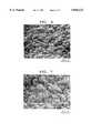
- FIGS. 6 and 7are scanning electron micrographs of diamond film surfaces before and after polishing.
- FIG. 1is a block diagram of the steps in fine polishing a surface of metal-soluble material.
- the first step (block A)is to provide a surface of metal-soluble material to be polished.
- Exemplary metal-soluble materialsinclude diamond and nitrides.
- a materialis metal soluble for these purposes if it has a solid solubility of at least 0.01 atomic percent in the metal at a temperature of 200° C. or less.
- the surfacecan be composed of polycrystalline or single crystal material. Typically it will be a diamond film, either as deposited or with a semi-finished surface condition ready for final polishing. It is preferred that the surface to be polished have a starting surface roughness on the order of a few microns or less but more than about 50 angstroms.
- Surface roughness referred to hereinis the root-mean-square (r.m.s.) surface roughness as measured by atomic force microscopy.
- Such a semi-finished surfacecan be obtained by conventional mechanical polishing or by the aforementioned high-temperature ( ⁇ 700°-900° C.) diffusion reactions.
- the material to be polishedmay have flat, curved or wavy surfaces depending on the specific application. Curved surfaces, for example, are useful for refractive diamond lenses. Wavy surfaces are useful in diamond Fresnel lenses. Both curved and wavy surfaces can be finish-polished to have desired smooth (but non-flat) surfaces.
- the second step(Block B in FIG. 1) is to apply to the surface to be polished a mixture of metal powder and a metal-dissolving carrier (acidic or basic).
- the polishing mediumcan be prepared by mixing fine powder of metal with the carrier.
- Carbon-dissolving metals for polishing diamondinclude transition metals such as Mn or Fe or alloys thereof, and rare earth metals such as Ce, La, Y, or alloys thereof (mischmetal, La--Ni, Ce--Ag alloys).
- Mnis a preferred carbon-dissolving metal because it exhibits high solubility of carbon even at relatively low temperatures below ⁇ 200° C. (See “Binary Alloy Phase Diagrams", ASM International, 1990, p. 860).
- the carbon-dissolving metal powderstypically have maximum particle size predominantly (>90% by weight) in the range of 1-1000 ⁇ m, and preferably in the range 5-200 ⁇ m.
- Other non-active fine particlessuch as silica (SiO 2 ) or alumina (Al 2 O 3 ) may be added for the purpose of controlling the viscosity of the polishing medium and for ease of handling.
- the preferred metal-dissolving carrieris a liquid acidic carrier such as hydrochloric acid, nitric acid, sulfuric acid, hydrofluoric acid, acetic acid or mixtures thereof. Desired concentration of the acid is typically in the range of 1-50 volume percent in water.
- the carriermakes the polishing reaction possible. It is a carrier for the metal powder, and it continuously etches off the surface oxide on the metal powder (the presence of which would interfere with the metal-carbon interaction for diamond dissolution and stop the polishing). It also continuously etches off the reaction product e.g., the carbon-containing Mn layer on the surface of Mn particles or on the diamond surface. The carrier thus continuously exposes fresh metal and fresh diamond surface to allow the polishing reactions to continue.
- the third step in FIG. 1is to polish the surface by rubbing.
- High speed rotating or reciprocating pads or rubbing brushesmay be used.
- the desired speed of brush motionis in the range of 10-10,000 rpm rotation or equivalent linear speed, and preferably in the range of 100-1000 rpm.
- polishingis not completely understood, but it is believed that there is instantaneous, atomic-scale heating during abrasion of the metal powder against the elevated portions of the material surface. This abrasion causes, at the contact points atomic-scale dissolution of the material into the metal, resulting in an atomic-scale polishing.
- the temperature of the polishing mediumis preferably kept near ambient room temperature for the sake of convenience, but it can be raised to as high as ⁇ 200° C. if a high polishing rate is desired.
- the brushis preferably made up of a chemically inactive (e.g. acid or base resistant) polymer, plastic, or glass fiber. Brushes may also be made of acid-resistant stainless steel, aluminum, or titanium alloy. Alternatively, the brush itself can also be made of carbon-dissolving metal, such as Mn, Fe, or their alloys. In such case the brush metals actively participate in the polishing reaction as a consumable material.
- the present polishing techniquecan be used not only for diamond but also for carbide materials. It can also be applied to nitride materials by using powders of metals with relatively high solid solubility of nitrogen at low temperatures.
- Preferred nitrogen-dissolving metalsinclude V, Zr, Fe, Ce, La or their alloys. Technologically important nitrides such as cubic-BN, AlN, GaN, InN or their alloys can be fine polished for electronic, optical and acoustical applications. In this case, the metal removes the nitrogen part and the acid removes the metallic element part from the nitride being polished.
- a base carriersuch as a NaOH or KOH solution
- acidis preferred over acid since Al is relatively resistant to acid etching but dissolves easily in these base solutions.
- the thermodynamic conditions of the specific involved materials under the local abrasion contact conditionsi.e., local instantaneous temperature and pressure
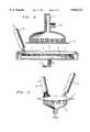
- FIG. 2illustrates preferred apparatus useful in practicing the method of FIG. 1.
- the apparatuscomprises a support member 10 such as a rotatable plate for holding one or more samples 11 to be polished (e.g. diamond films), a conduit such as tube 12 for applying the polishing medium, and a movable polishing member 13 such as a rotatable brush.
- the plate 10is preferably made of or coated with non-corrosive materials, such as glass, ceramic, polymer, stainless steel or aluminum.
- the samples 11are mounted on the plate 10 and the polishing medium (preferably Mn-powder/acid for diamond) is supplied through tube 12. The plate is rotated, and the samples are polished by brush 13.
- the polishing mediumpreferably Mn-powder/acid for diamond
- FIG. 3is a polishing apparatus suitable for continuous operation.
- samples 30are placed in a series of containers 31 which in turn are placed on a movable conveyer belt 32.
- One or more tubes(not shown) are provided for continuously supplying the polishing medium onto the sample surface.
- the samplesare polished by rotating brushes 33 that advantageously travel at the same speed as the conveyer belt.
- FIG. 4shows a third polishing apparatus.
- the samples 40can be held upside down on the bottom of vacuum suction holder 41, which is then lowered onto a rotating polishing pad or brush 42 wet with the polishing medium via tube 43.
- the samplecan be placed on the bottom of the sample holder by mechanical means or by gluing.
- FIG. 5shows an alternative polishing apparatus particularly useful for polishing non-planar surfaces such as lenses.
- the apparatuscomprises a sample holder 50 such as a vacuum holder for holding a lens 51, a tube 52 for delivering the polishing medium, and a polishing element 53 such as a rotating brush.
- a CVD diamond film deposited on a smooth Si substratewas cut into 1 cm ⁇ 1 cm squares.
- the filmhad a surface roughness of ⁇ 90 ⁇ . It was polished by using a slurry mixture consisting of about 25 volume percent of Mn powder (average particle diameter less than 45 ⁇ m) and about 75 volume percent of 10% hydrochloric acid in distilled water.
- a rotating brush( ⁇ 300 rpm) was used to rub the polishing medium against the diamond surface for a duration of 30 minutes.
- the root-mean-square surface roughness as measured by atomic force microscopywas reduced from ⁇ 90 ⁇ to ⁇ 70 ⁇ by the polishing.
- FIGS. 6 and 7are SEM photomicrographs which illustrate the surface morphology of a sample before and after the polishing.
- the polished sample(FIG. 7) shows more smooth area as compared to the unpolished sample (FIG. 6).
- Atomic force microscopy on the smooth regions of the polished sample in FIG. 7 sampleshows a surface roughness of about 30 ⁇ .
Landscapes
- Engineering & Computer Science (AREA)
- Mechanical Engineering (AREA)
- Finish Polishing, Edge Sharpening, And Grinding By Specific Grinding Devices (AREA)
- Grinding And Polishing Of Tertiary Curved Surfaces And Surfaces With Complex Shapes (AREA)
- Crystals, And After-Treatments Of Crystals (AREA)
Abstract
Description
Claims (7)
Priority Applications (4)
| Application Number | Priority Date | Filing Date | Title |
|---|---|---|---|
| US08/429,259US5846122A (en) | 1995-04-25 | 1995-04-25 | Method and apparatus for polishing metal-soluble materials such as diamond |
| CA002169392ACA2169392A1 (en) | 1995-04-25 | 1996-02-13 | Method and apparatus for polishing metal-soluble materials such as diamond |
| JP8093702AJPH08336739A (en) | 1995-04-25 | 1996-04-16 | Polishing method for molten metal material and its apparatus |
| EP96302678AEP0739686A3 (en) | 1995-04-25 | 1996-04-17 | Method and apparatus for polishing metal-soluble materials such as diamond |
Applications Claiming Priority (1)
| Application Number | Priority Date | Filing Date | Title |
|---|---|---|---|
| US08/429,259US5846122A (en) | 1995-04-25 | 1995-04-25 | Method and apparatus for polishing metal-soluble materials such as diamond |
Publications (1)
| Publication Number | Publication Date |
|---|---|
| US5846122Atrue US5846122A (en) | 1998-12-08 |
Family
ID=23702495
Family Applications (1)
| Application Number | Title | Priority Date | Filing Date |
|---|---|---|---|
| US08/429,259Expired - LifetimeUS5846122A (en) | 1995-04-25 | 1995-04-25 | Method and apparatus for polishing metal-soluble materials such as diamond |
Country Status (4)
| Country | Link |
|---|---|
| US (1) | US5846122A (en) |
| EP (1) | EP0739686A3 (en) |
| JP (1) | JPH08336739A (en) |
| CA (1) | CA2169392A1 (en) |
Cited By (8)
| Publication number | Priority date | Publication date | Assignee | Title |
|---|---|---|---|---|
| US6126514A (en)* | 1998-03-12 | 2000-10-03 | Sony Corporation | Polishing slurry and polishing method using the same |
| US6302768B1 (en)* | 1997-11-17 | 2001-10-16 | Mitsubishi Materials Corporation | Method for polishing surface of vapor-phase synthesized thin diamond film |
| US6582279B1 (en)* | 2002-03-07 | 2003-06-24 | Hitachi Global Storage Technologies Netherlands B.V. | Apparatus and method for reclaiming a disk substrate for use in a data storage device |
| US20040058629A1 (en)* | 2002-09-25 | 2004-03-25 | Georg Weber | Apparatus for processing substantially planar workpieces |
| US20060151433A1 (en)* | 2005-01-10 | 2006-07-13 | Chi-Lung Chang | Method for removing and recoating of diamond-like carbon films and its products thereof |
| US20070204880A1 (en)* | 2006-03-01 | 2007-09-06 | Fraunhofer-Gesellschaft Zur Forderung Der Angewandten Forshung E.V. | Method of working surfaces of a coating made of hard carbon |
| US20110300785A1 (en)* | 2008-12-22 | 2011-12-08 | Peter Wolters Gmbh | Apparatus for Double-Sided, Grinding Machining of Flat Workpieces |
| US20180051367A1 (en)* | 2015-03-11 | 2018-02-22 | Fraunhofer-Gesellschaft Zur Foerderung Der Angewandten Forschung E.V. | Method for a defined surface treatment of a first carbon coating applied on a surface of a component |
Families Citing this family (4)
| Publication number | Priority date | Publication date | Assignee | Title |
|---|---|---|---|---|
| JPH11347921A (en)* | 1998-06-05 | 1999-12-21 | Memc Kk | Abrasive method for silicon wafer |
| KR101508917B1 (en)* | 2009-03-13 | 2015-04-07 | 생-고뱅 세라믹스 앤드 플라스틱스, 인코포레이티드 | Chemical mechanical planarization using nanodiamond |
| RU2483856C2 (en)* | 2011-07-07 | 2013-06-10 | Российская Федерация, от имени которой выступает Министерство промышленности и торговли РФ | Method of grinding diamond plates |
| EP3516002B1 (en) | 2016-09-23 | 2022-01-05 | Saint-Gobain Ceramics & Plastics, Inc. | Chemical mechanical planarization slurry and method for forming same |
Citations (17)
| Publication number | Priority date | Publication date | Assignee | Title |
|---|---|---|---|---|
| US4475981A (en)* | 1983-10-28 | 1984-10-09 | Ampex Corporation | Metal polishing composition and process |
| US4601134A (en)* | 1984-01-21 | 1986-07-22 | Karl Heesemann Maschinenfabrik Gmbh & Co. Kg | Belt grinder having pressure pads with individually variable contact pressures |
| US4645561A (en)* | 1986-01-06 | 1987-02-24 | Ampex Corporation | Metal-polishing composition and process |
| JPS6471653A (en)* | 1987-09-09 | 1989-03-16 | Sumitomo Electric Industries | Method for polishing diamond |
| EP0366027A2 (en)* | 1988-10-28 | 1990-05-02 | International Business Machines Corporation | Wafer flood polishing |
| JPH02119136A (en)* | 1988-10-28 | 1990-05-07 | Sony Corp | Abrasive surface plate for semiconductor layer |
| US5064683A (en)* | 1990-10-29 | 1991-11-12 | Motorola, Inc. | Method for polish planarizing a semiconductor substrate by using a boron nitride polish stop |
| US5142828A (en)* | 1990-06-25 | 1992-09-01 | Microelectronics And Computer Technology Corporation | Correcting a defective metallization layer on an electronic component by polishing |
| US5149338A (en)* | 1991-07-22 | 1992-09-22 | Fulton Kenneth W | Superpolishing agent, process for polishing hard ceramic materials, and polished hard ceramics |
| US5154023A (en)* | 1991-06-11 | 1992-10-13 | Spire Corporation | Polishing process for refractory materials |
| US5154021A (en)* | 1991-06-26 | 1992-10-13 | International Business Machines Corporation | Pneumatic pad conditioner |
| JPH04370948A (en)* | 1991-06-19 | 1992-12-24 | Nec Corp | Evaluation of semiconductor crystal dislocation |
| JPH05102053A (en)* | 1991-10-03 | 1993-04-23 | Hitachi Cable Ltd | Compound semiconductor wafer and method of manufacturing the same |
| US5207759A (en)* | 1991-09-20 | 1993-05-04 | Hmt Technology Corporation | Texturing slurry and method |
| EP0618043A1 (en)* | 1993-03-29 | 1994-10-05 | AT&T Corp. | Article comprising polycrystalline diamond, and method of shaping the diamond |
| US5506061A (en)* | 1989-07-06 | 1996-04-09 | Forskningscenter Riso | Method for the preparation of metal matrix composite materials |
| US5538462A (en)* | 1994-03-15 | 1996-07-23 | The Gleason Works | Lapping compound supply system for a gear finishing machine |
- 1995
- 1995-04-25USUS08/429,259patent/US5846122A/ennot_activeExpired - Lifetime
- 1996
- 1996-02-13CACA002169392Apatent/CA2169392A1/ennot_activeAbandoned
- 1996-04-16JPJP8093702Apatent/JPH08336739A/enactivePending
- 1996-04-17EPEP96302678Apatent/EP0739686A3/ennot_activeWithdrawn
Patent Citations (17)
| Publication number | Priority date | Publication date | Assignee | Title |
|---|---|---|---|---|
| US4475981A (en)* | 1983-10-28 | 1984-10-09 | Ampex Corporation | Metal polishing composition and process |
| US4601134A (en)* | 1984-01-21 | 1986-07-22 | Karl Heesemann Maschinenfabrik Gmbh & Co. Kg | Belt grinder having pressure pads with individually variable contact pressures |
| US4645561A (en)* | 1986-01-06 | 1987-02-24 | Ampex Corporation | Metal-polishing composition and process |
| JPS6471653A (en)* | 1987-09-09 | 1989-03-16 | Sumitomo Electric Industries | Method for polishing diamond |
| EP0366027A2 (en)* | 1988-10-28 | 1990-05-02 | International Business Machines Corporation | Wafer flood polishing |
| JPH02119136A (en)* | 1988-10-28 | 1990-05-07 | Sony Corp | Abrasive surface plate for semiconductor layer |
| US5506061A (en)* | 1989-07-06 | 1996-04-09 | Forskningscenter Riso | Method for the preparation of metal matrix composite materials |
| US5142828A (en)* | 1990-06-25 | 1992-09-01 | Microelectronics And Computer Technology Corporation | Correcting a defective metallization layer on an electronic component by polishing |
| US5064683A (en)* | 1990-10-29 | 1991-11-12 | Motorola, Inc. | Method for polish planarizing a semiconductor substrate by using a boron nitride polish stop |
| US5154023A (en)* | 1991-06-11 | 1992-10-13 | Spire Corporation | Polishing process for refractory materials |
| JPH04370948A (en)* | 1991-06-19 | 1992-12-24 | Nec Corp | Evaluation of semiconductor crystal dislocation |
| US5154021A (en)* | 1991-06-26 | 1992-10-13 | International Business Machines Corporation | Pneumatic pad conditioner |
| US5149338A (en)* | 1991-07-22 | 1992-09-22 | Fulton Kenneth W | Superpolishing agent, process for polishing hard ceramic materials, and polished hard ceramics |
| US5207759A (en)* | 1991-09-20 | 1993-05-04 | Hmt Technology Corporation | Texturing slurry and method |
| JPH05102053A (en)* | 1991-10-03 | 1993-04-23 | Hitachi Cable Ltd | Compound semiconductor wafer and method of manufacturing the same |
| EP0618043A1 (en)* | 1993-03-29 | 1994-10-05 | AT&T Corp. | Article comprising polycrystalline diamond, and method of shaping the diamond |
| US5538462A (en)* | 1994-03-15 | 1996-07-23 | The Gleason Works | Lapping compound supply system for a gear finishing machine |
Non-Patent Citations (4)
| Title |
|---|
| S. Jim et al. "Shaping of diamond films by etching with molten rare-earth metals, Nature, vol. 362, pp. 822-824 (1993). |
| S. Jim et al. Shaping of diamond films by etching with molten rare earth metals, Nature, vol. 362, pp. 822 824 (1993).* |
| S. Jin et al. "Polishing of CVD diamond by diffusional reaction with manganese powder, Diamond and Related Materials, vol. 1, pp. 949-953 (1992). |
| S. Jin et al. Polishing of CVD diamond by diffusional reaction with manganese powder, Diamond and Related Materials, vol. 1, pp. 949 953 (1992).* |
Cited By (11)
| Publication number | Priority date | Publication date | Assignee | Title |
|---|---|---|---|---|
| US6302768B1 (en)* | 1997-11-17 | 2001-10-16 | Mitsubishi Materials Corporation | Method for polishing surface of vapor-phase synthesized thin diamond film |
| US6126514A (en)* | 1998-03-12 | 2000-10-03 | Sony Corporation | Polishing slurry and polishing method using the same |
| US6582279B1 (en)* | 2002-03-07 | 2003-06-24 | Hitachi Global Storage Technologies Netherlands B.V. | Apparatus and method for reclaiming a disk substrate for use in a data storage device |
| US20040058629A1 (en)* | 2002-09-25 | 2004-03-25 | Georg Weber | Apparatus for processing substantially planar workpieces |
| US6986703B2 (en)* | 2002-09-25 | 2006-01-17 | Georg Weber | Apparatus for processing substantially planar workpieces |
| US20060151433A1 (en)* | 2005-01-10 | 2006-07-13 | Chi-Lung Chang | Method for removing and recoating of diamond-like carbon films and its products thereof |
| US20070204880A1 (en)* | 2006-03-01 | 2007-09-06 | Fraunhofer-Gesellschaft Zur Forderung Der Angewandten Forshung E.V. | Method of working surfaces of a coating made of hard carbon |
| US20110300785A1 (en)* | 2008-12-22 | 2011-12-08 | Peter Wolters Gmbh | Apparatus for Double-Sided, Grinding Machining of Flat Workpieces |
| US9004981B2 (en)* | 2008-12-22 | 2015-04-14 | Peter Wolters Gmbh | Apparatus for double-sided, grinding machining of flat workpieces |
| US20180051367A1 (en)* | 2015-03-11 | 2018-02-22 | Fraunhofer-Gesellschaft Zur Foerderung Der Angewandten Forschung E.V. | Method for a defined surface treatment of a first carbon coating applied on a surface of a component |
| US10633735B2 (en)* | 2015-03-11 | 2020-04-28 | Fraunhofer-Gesellschaft Zur Foerderung Der Angewandten Forschung E.V. | Method for a defined surface treatment of a first carbon coating applied on a surface of a component |
Also Published As
| Publication number | Publication date |
|---|---|
| JPH08336739A (en) | 1996-12-24 |
| CA2169392A1 (en) | 1996-10-26 |
| EP0739686A3 (en) | 1996-11-13 |
| EP0739686A2 (en) | 1996-10-30 |
Similar Documents
| Publication | Publication Date | Title |
|---|---|---|
| US5674107A (en) | Diamond polishing method and apparatus employing oxygen-emitting medium | |
| US5846122A (en) | Method and apparatus for polishing metal-soluble materials such as diamond | |
| KR0147144B1 (en) | Wafer coated with hard material, manufacturing method thereof, polishing device for wafer coated with hard material, and manufacturing method thereof | |
| US5645736A (en) | Method for polishing a wafer | |
| JP3121274B2 (en) | Polishing composition | |
| US7367875B2 (en) | CVD diamond-coated composite substrate containing a carbide-forming material and ceramic phases and method for making same | |
| US5746931A (en) | Method and apparatus for chemical-mechanical polishing of diamond | |
| JP5518871B2 (en) | Abrasive grains with unique morphology | |
| CN108527182B (en) | Method for preparing diamond abrasive tool with orderly arrangement of abrasive grains by using mask | |
| EP1917122A2 (en) | Use of cmp for aluminum mirror and solar cell fabrication | |
| JP2002222780A (en) | Surface polishing method for silicon wafer | |
| EP1015175A1 (en) | Abrasive articles comprising a fluorochemical agent for wafer surface modification | |
| EP0121706A2 (en) | Method for polishing titanium carbide containing surfaces | |
| JP2007311586A (en) | Finish polishing method for silicon carbide single crystal wafer surface | |
| TW200411754A (en) | A method of polishing a wafer of material | |
| TW568813B (en) | Polishing agent, method of producing this agent, and method of polishing | |
| WO2007063873A1 (en) | Polishing method and polishing apparatus | |
| US5425965A (en) | Process for deposition of ultra-fine grained polycrystalline diamond films | |
| US20030006396A1 (en) | Polishing composition for CMP having abrasive particles | |
| JP2008288240A (en) | SiC crystal polishing method | |
| JP2002346915A (en) | Chemical mechanical polishing method of diamond thin film | |
| JP3857742B2 (en) | Glass mold for optical element molding | |
| JPH06262525A (en) | Grinding wheel and manufacturing method thereof | |
| TWI863013B (en) | Method for polishing diamond surface and polycrystalline alumina surface | |
| JP4554799B2 (en) | Polishing tool based on fluororesin |
Legal Events
| Date | Code | Title | Description |
|---|---|---|---|
| AS | Assignment | Owner name:AT&T IPM CORP., FLORIDA Free format text:ASSIGNMENT OF ASSIGNORS INTEREST;ASSIGNORS:GRARBNER, JOHN EDWIN;JIN, SUNGHO;KAMMLOTT, GUENTHER WILHELM;AND OTHERS;REEL/FRAME:007459/0217;SIGNING DATES FROM 19950421 TO 19950424 | |
| AS | Assignment | Owner name:LUCENT TECHNOLOGIES INC., NEW JERSEY Free format text:ASSIGNMENT OF ASSIGNORS INTEREST;ASSIGNOR:AT&T CORP.;REEL/FRAME:008681/0838 Effective date:19960329 | |
| STCF | Information on status: patent grant | Free format text:PATENTED CASE | |
| FPAY | Fee payment | Year of fee payment:4 | |
| FPAY | Fee payment | Year of fee payment:8 | |
| FPAY | Fee payment | Year of fee payment:12 | |
| AS | Assignment | Owner name:DEUTSCHE BANK AG NEW YORK BRANCH, AS COLLATERAL AG Free format text:PATENT SECURITY AGREEMENT;ASSIGNORS:LSI CORPORATION;AGERE SYSTEMS LLC;REEL/FRAME:032856/0031 Effective date:20140506 | |
| AS | Assignment | Owner name:AVAGO TECHNOLOGIES GENERAL IP (SINGAPORE) PTE. LTD Free format text:ASSIGNMENT OF ASSIGNORS INTEREST;ASSIGNOR:AGERE SYSTEMS LLC;REEL/FRAME:035365/0634 Effective date:20140804 | |
| AS | Assignment | Owner name:LSI CORPORATION, CALIFORNIA Free format text:TERMINATION AND RELEASE OF SECURITY INTEREST IN PATENT RIGHTS (RELEASES RF 032856-0031);ASSIGNOR:DEUTSCHE BANK AG NEW YORK BRANCH, AS COLLATERAL AGENT;REEL/FRAME:037684/0039 Effective date:20160201 Owner name:AGERE SYSTEMS LLC, PENNSYLVANIA Free format text:TERMINATION AND RELEASE OF SECURITY INTEREST IN PATENT RIGHTS (RELEASES RF 032856-0031);ASSIGNOR:DEUTSCHE BANK AG NEW YORK BRANCH, AS COLLATERAL AGENT;REEL/FRAME:037684/0039 Effective date:20160201 | |
| AS | Assignment | Owner name:BANK OF AMERICA, N.A., AS COLLATERAL AGENT, NORTH CAROLINA Free format text:PATENT SECURITY AGREEMENT;ASSIGNOR:AVAGO TECHNOLOGIES GENERAL IP (SINGAPORE) PTE. LTD.;REEL/FRAME:037808/0001 Effective date:20160201 Owner name:BANK OF AMERICA, N.A., AS COLLATERAL AGENT, NORTH Free format text:PATENT SECURITY AGREEMENT;ASSIGNOR:AVAGO TECHNOLOGIES GENERAL IP (SINGAPORE) PTE. LTD.;REEL/FRAME:037808/0001 Effective date:20160201 | |
| AS | Assignment | Owner name:AVAGO TECHNOLOGIES GENERAL IP (SINGAPORE) PTE. LTD., SINGAPORE Free format text:TERMINATION AND RELEASE OF SECURITY INTEREST IN PATENTS;ASSIGNOR:BANK OF AMERICA, N.A., AS COLLATERAL AGENT;REEL/FRAME:041710/0001 Effective date:20170119 Owner name:AVAGO TECHNOLOGIES GENERAL IP (SINGAPORE) PTE. LTD Free format text:TERMINATION AND RELEASE OF SECURITY INTEREST IN PATENTS;ASSIGNOR:BANK OF AMERICA, N.A., AS COLLATERAL AGENT;REEL/FRAME:041710/0001 Effective date:20170119 |