US5843808A - Structure and method for automated assembly of a tab grid array package - Google Patents
Structure and method for automated assembly of a tab grid array packageDownload PDFInfo
- Publication number
- US5843808A US5843808AUS08/585,134US58513496AUS5843808AUS 5843808 AUS5843808 AUS 5843808AUS 58513496 AUS58513496 AUS 58513496AUS 5843808 AUS5843808 AUS 5843808A
- Authority
- US
- United States
- Prior art keywords
- package
- tape
- solder balls
- tga
- stiffener
- Prior art date
- Legal status (The legal status is an assumption and is not a legal conclusion. Google has not performed a legal analysis and makes no representation as to the accuracy of the status listed.)
- Expired - Lifetime
Links
Images


Classifications
- H—ELECTRICITY
- H01—ELECTRIC ELEMENTS
- H01L—SEMICONDUCTOR DEVICES NOT COVERED BY CLASS H10
- H01L24/00—Arrangements for connecting or disconnecting semiconductor or solid-state bodies; Methods or apparatus related thereto
- H01L24/01—Means for bonding being attached to, or being formed on, the surface to be connected, e.g. chip-to-package, die-attach, "first-level" interconnects; Manufacturing methods related thereto
- H01L24/42—Wire connectors; Manufacturing methods related thereto
- H01L24/47—Structure, shape, material or disposition of the wire connectors after the connecting process
- H01L24/49—Structure, shape, material or disposition of the wire connectors after the connecting process of a plurality of wire connectors
- H—ELECTRICITY
- H01—ELECTRIC ELEMENTS
- H01L—SEMICONDUCTOR DEVICES NOT COVERED BY CLASS H10
- H01L23/00—Details of semiconductor or other solid state devices
- H01L23/48—Arrangements for conducting electric current to or from the solid state body in operation, e.g. leads, terminal arrangements ; Selection of materials therefor
- H01L23/488—Arrangements for conducting electric current to or from the solid state body in operation, e.g. leads, terminal arrangements ; Selection of materials therefor consisting of soldered or bonded constructions
- H01L23/498—Leads, i.e. metallisations or lead-frames on insulating substrates, e.g. chip carriers
- H01L23/49811—Additional leads joined to the metallisation on the insulating substrate, e.g. pins, bumps, wires, flat leads
- H01L23/49816—Spherical bumps on the substrate for external connection, e.g. ball grid arrays [BGA]
- H—ELECTRICITY
- H01—ELECTRIC ELEMENTS
- H01L—SEMICONDUCTOR DEVICES NOT COVERED BY CLASS H10
- H01L23/00—Details of semiconductor or other solid state devices
- H01L23/48—Arrangements for conducting electric current to or from the solid state body in operation, e.g. leads, terminal arrangements ; Selection of materials therefor
- H01L23/488—Arrangements for conducting electric current to or from the solid state body in operation, e.g. leads, terminal arrangements ; Selection of materials therefor consisting of soldered or bonded constructions
- H01L23/498—Leads, i.e. metallisations or lead-frames on insulating substrates, e.g. chip carriers
- H01L23/49838—Geometry or layout
- H—ELECTRICITY
- H01—ELECTRIC ELEMENTS
- H01L—SEMICONDUCTOR DEVICES NOT COVERED BY CLASS H10
- H01L23/00—Details of semiconductor or other solid state devices
- H01L23/48—Arrangements for conducting electric current to or from the solid state body in operation, e.g. leads, terminal arrangements ; Selection of materials therefor
- H01L23/488—Arrangements for conducting electric current to or from the solid state body in operation, e.g. leads, terminal arrangements ; Selection of materials therefor consisting of soldered or bonded constructions
- H01L23/498—Leads, i.e. metallisations or lead-frames on insulating substrates, e.g. chip carriers
- H01L23/4985—Flexible insulating substrates
- H—ELECTRICITY
- H01—ELECTRIC ELEMENTS
- H01L—SEMICONDUCTOR DEVICES NOT COVERED BY CLASS H10
- H01L23/00—Details of semiconductor or other solid state devices
- H01L23/48—Arrangements for conducting electric current to or from the solid state body in operation, e.g. leads, terminal arrangements ; Selection of materials therefor
- H01L23/50—Arrangements for conducting electric current to or from the solid state body in operation, e.g. leads, terminal arrangements ; Selection of materials therefor for integrated circuit devices, e.g. power bus, number of leads
- B—PERFORMING OPERATIONS; TRANSPORTING
- B29—WORKING OF PLASTICS; WORKING OF SUBSTANCES IN A PLASTIC STATE IN GENERAL
- B29C—SHAPING OR JOINING OF PLASTICS; SHAPING OF MATERIAL IN A PLASTIC STATE, NOT OTHERWISE PROVIDED FOR; AFTER-TREATMENT OF THE SHAPED PRODUCTS, e.g. REPAIRING
- B29C43/00—Compression moulding, i.e. applying external pressure to flow the moulding material; Apparatus therefor
- B29C43/32—Component parts, details or accessories; Auxiliary operations
- B29C43/58—Measuring, controlling or regulating
- B29C2043/5825—Measuring, controlling or regulating dimensions or shape, e.g. size, thickness
- H—ELECTRICITY
- H01—ELECTRIC ELEMENTS
- H01L—SEMICONDUCTOR DEVICES NOT COVERED BY CLASS H10
- H01L2224/00—Indexing scheme for arrangements for connecting or disconnecting semiconductor or solid-state bodies and methods related thereto as covered by H01L24/00
- H01L2224/01—Means for bonding being attached to, or being formed on, the surface to be connected, e.g. chip-to-package, die-attach, "first-level" interconnects; Manufacturing methods related thereto
- H01L2224/26—Layer connectors, e.g. plate connectors, solder or adhesive layers; Manufacturing methods related thereto
- H01L2224/31—Structure, shape, material or disposition of the layer connectors after the connecting process
- H01L2224/32—Structure, shape, material or disposition of the layer connectors after the connecting process of an individual layer connector
- H01L2224/321—Disposition
- H01L2224/32151—Disposition the layer connector connecting between a semiconductor or solid-state body and an item not being a semiconductor or solid-state body, e.g. chip-to-substrate, chip-to-passive
- H01L2224/32221—Disposition the layer connector connecting between a semiconductor or solid-state body and an item not being a semiconductor or solid-state body, e.g. chip-to-substrate, chip-to-passive the body and the item being stacked
- H01L2224/32245—Disposition the layer connector connecting between a semiconductor or solid-state body and an item not being a semiconductor or solid-state body, e.g. chip-to-substrate, chip-to-passive the body and the item being stacked the item being metallic
- H—ELECTRICITY
- H01—ELECTRIC ELEMENTS
- H01L—SEMICONDUCTOR DEVICES NOT COVERED BY CLASS H10
- H01L2224/00—Indexing scheme for arrangements for connecting or disconnecting semiconductor or solid-state bodies and methods related thereto as covered by H01L24/00
- H01L2224/01—Means for bonding being attached to, or being formed on, the surface to be connected, e.g. chip-to-package, die-attach, "first-level" interconnects; Manufacturing methods related thereto
- H01L2224/42—Wire connectors; Manufacturing methods related thereto
- H01L2224/44—Structure, shape, material or disposition of the wire connectors prior to the connecting process
- H01L2224/45—Structure, shape, material or disposition of the wire connectors prior to the connecting process of an individual wire connector
- H01L2224/45001—Core members of the connector
- H01L2224/45099—Material
- H01L2224/451—Material with a principal constituent of the material being a metal or a metalloid, e.g. boron (B), silicon (Si), germanium (Ge), arsenic (As), antimony (Sb), tellurium (Te) and polonium (Po), and alloys thereof
- H01L2224/45138—Material with a principal constituent of the material being a metal or a metalloid, e.g. boron (B), silicon (Si), germanium (Ge), arsenic (As), antimony (Sb), tellurium (Te) and polonium (Po), and alloys thereof the principal constituent melting at a temperature of greater than or equal to 950°C and less than 1550°C
- H01L2224/45144—Gold (Au) as principal constituent
- H—ELECTRICITY
- H01—ELECTRIC ELEMENTS
- H01L—SEMICONDUCTOR DEVICES NOT COVERED BY CLASS H10
- H01L2224/00—Indexing scheme for arrangements for connecting or disconnecting semiconductor or solid-state bodies and methods related thereto as covered by H01L24/00
- H01L2224/01—Means for bonding being attached to, or being formed on, the surface to be connected, e.g. chip-to-package, die-attach, "first-level" interconnects; Manufacturing methods related thereto
- H01L2224/42—Wire connectors; Manufacturing methods related thereto
- H01L2224/47—Structure, shape, material or disposition of the wire connectors after the connecting process
- H01L2224/48—Structure, shape, material or disposition of the wire connectors after the connecting process of an individual wire connector
- H01L2224/4805—Shape
- H01L2224/4809—Loop shape
- H01L2224/48091—Arched
- H—ELECTRICITY
- H01—ELECTRIC ELEMENTS
- H01L—SEMICONDUCTOR DEVICES NOT COVERED BY CLASS H10
- H01L2224/00—Indexing scheme for arrangements for connecting or disconnecting semiconductor or solid-state bodies and methods related thereto as covered by H01L24/00
- H01L2224/01—Means for bonding being attached to, or being formed on, the surface to be connected, e.g. chip-to-package, die-attach, "first-level" interconnects; Manufacturing methods related thereto
- H01L2224/42—Wire connectors; Manufacturing methods related thereto
- H01L2224/47—Structure, shape, material or disposition of the wire connectors after the connecting process
- H01L2224/48—Structure, shape, material or disposition of the wire connectors after the connecting process of an individual wire connector
- H01L2224/481—Disposition
- H01L2224/48151—Connecting between a semiconductor or solid-state body and an item not being a semiconductor or solid-state body, e.g. chip-to-substrate, chip-to-passive
- H01L2224/48221—Connecting between a semiconductor or solid-state body and an item not being a semiconductor or solid-state body, e.g. chip-to-substrate, chip-to-passive the body and the item being stacked
- H01L2224/48225—Connecting between a semiconductor or solid-state body and an item not being a semiconductor or solid-state body, e.g. chip-to-substrate, chip-to-passive the body and the item being stacked the item being non-metallic, e.g. insulating substrate with or without metallisation
- H01L2224/48227—Connecting between a semiconductor or solid-state body and an item not being a semiconductor or solid-state body, e.g. chip-to-substrate, chip-to-passive the body and the item being stacked the item being non-metallic, e.g. insulating substrate with or without metallisation connecting the wire to a bond pad of the item
- H—ELECTRICITY
- H01—ELECTRIC ELEMENTS
- H01L—SEMICONDUCTOR DEVICES NOT COVERED BY CLASS H10
- H01L2224/00—Indexing scheme for arrangements for connecting or disconnecting semiconductor or solid-state bodies and methods related thereto as covered by H01L24/00
- H01L2224/01—Means for bonding being attached to, or being formed on, the surface to be connected, e.g. chip-to-package, die-attach, "first-level" interconnects; Manufacturing methods related thereto
- H01L2224/42—Wire connectors; Manufacturing methods related thereto
- H01L2224/47—Structure, shape, material or disposition of the wire connectors after the connecting process
- H01L2224/48—Structure, shape, material or disposition of the wire connectors after the connecting process of an individual wire connector
- H01L2224/481—Disposition
- H01L2224/48151—Connecting between a semiconductor or solid-state body and an item not being a semiconductor or solid-state body, e.g. chip-to-substrate, chip-to-passive
- H01L2224/48221—Connecting between a semiconductor or solid-state body and an item not being a semiconductor or solid-state body, e.g. chip-to-substrate, chip-to-passive the body and the item being stacked
- H01L2224/48245—Connecting between a semiconductor or solid-state body and an item not being a semiconductor or solid-state body, e.g. chip-to-substrate, chip-to-passive the body and the item being stacked the item being metallic
- H01L2224/48247—Connecting between a semiconductor or solid-state body and an item not being a semiconductor or solid-state body, e.g. chip-to-substrate, chip-to-passive the body and the item being stacked the item being metallic connecting the wire to a bond pad of the item
- H—ELECTRICITY
- H01—ELECTRIC ELEMENTS
- H01L—SEMICONDUCTOR DEVICES NOT COVERED BY CLASS H10
- H01L2224/00—Indexing scheme for arrangements for connecting or disconnecting semiconductor or solid-state bodies and methods related thereto as covered by H01L24/00
- H01L2224/01—Means for bonding being attached to, or being formed on, the surface to be connected, e.g. chip-to-package, die-attach, "first-level" interconnects; Manufacturing methods related thereto
- H01L2224/42—Wire connectors; Manufacturing methods related thereto
- H01L2224/47—Structure, shape, material or disposition of the wire connectors after the connecting process
- H01L2224/49—Structure, shape, material or disposition of the wire connectors after the connecting process of a plurality of wire connectors
- H01L2224/491—Disposition
- H01L2224/49105—Connecting at different heights
- H01L2224/49109—Connecting at different heights outside the semiconductor or solid-state body
- H—ELECTRICITY
- H01—ELECTRIC ELEMENTS
- H01L—SEMICONDUCTOR DEVICES NOT COVERED BY CLASS H10
- H01L2224/00—Indexing scheme for arrangements for connecting or disconnecting semiconductor or solid-state bodies and methods related thereto as covered by H01L24/00
- H01L2224/73—Means for bonding being of different types provided for in two or more of groups H01L2224/10, H01L2224/18, H01L2224/26, H01L2224/34, H01L2224/42, H01L2224/50, H01L2224/63, H01L2224/71
- H01L2224/732—Location after the connecting process
- H01L2224/73251—Location after the connecting process on different surfaces
- H01L2224/73265—Layer and wire connectors
- H—ELECTRICITY
- H01—ELECTRIC ELEMENTS
- H01L—SEMICONDUCTOR DEVICES NOT COVERED BY CLASS H10
- H01L24/00—Arrangements for connecting or disconnecting semiconductor or solid-state bodies; Methods or apparatus related thereto
- H01L24/01—Means for bonding being attached to, or being formed on, the surface to be connected, e.g. chip-to-package, die-attach, "first-level" interconnects; Manufacturing methods related thereto
- H01L24/42—Wire connectors; Manufacturing methods related thereto
- H01L24/44—Structure, shape, material or disposition of the wire connectors prior to the connecting process
- H01L24/45—Structure, shape, material or disposition of the wire connectors prior to the connecting process of an individual wire connector
- H—ELECTRICITY
- H01—ELECTRIC ELEMENTS
- H01L—SEMICONDUCTOR DEVICES NOT COVERED BY CLASS H10
- H01L24/00—Arrangements for connecting or disconnecting semiconductor or solid-state bodies; Methods or apparatus related thereto
- H01L24/01—Means for bonding being attached to, or being formed on, the surface to be connected, e.g. chip-to-package, die-attach, "first-level" interconnects; Manufacturing methods related thereto
- H01L24/42—Wire connectors; Manufacturing methods related thereto
- H01L24/47—Structure, shape, material or disposition of the wire connectors after the connecting process
- H01L24/48—Structure, shape, material or disposition of the wire connectors after the connecting process of an individual wire connector
- H—ELECTRICITY
- H01—ELECTRIC ELEMENTS
- H01L—SEMICONDUCTOR DEVICES NOT COVERED BY CLASS H10
- H01L24/00—Arrangements for connecting or disconnecting semiconductor or solid-state bodies; Methods or apparatus related thereto
- H01L24/73—Means for bonding being of different types provided for in two or more of groups H01L24/10, H01L24/18, H01L24/26, H01L24/34, H01L24/42, H01L24/50, H01L24/63, H01L24/71
- H—ELECTRICITY
- H01—ELECTRIC ELEMENTS
- H01L—SEMICONDUCTOR DEVICES NOT COVERED BY CLASS H10
- H01L2924/00—Indexing scheme for arrangements or methods for connecting or disconnecting semiconductor or solid-state bodies as covered by H01L24/00
- H01L2924/01—Chemical elements
- H01L2924/01005—Boron [B]
- H—ELECTRICITY
- H01—ELECTRIC ELEMENTS
- H01L—SEMICONDUCTOR DEVICES NOT COVERED BY CLASS H10
- H01L2924/00—Indexing scheme for arrangements or methods for connecting or disconnecting semiconductor or solid-state bodies as covered by H01L24/00
- H01L2924/01—Chemical elements
- H01L2924/01006—Carbon [C]
- H—ELECTRICITY
- H01—ELECTRIC ELEMENTS
- H01L—SEMICONDUCTOR DEVICES NOT COVERED BY CLASS H10
- H01L2924/00—Indexing scheme for arrangements or methods for connecting or disconnecting semiconductor or solid-state bodies as covered by H01L24/00
- H01L2924/01—Chemical elements
- H01L2924/01013—Aluminum [Al]
- H—ELECTRICITY
- H01—ELECTRIC ELEMENTS
- H01L—SEMICONDUCTOR DEVICES NOT COVERED BY CLASS H10
- H01L2924/00—Indexing scheme for arrangements or methods for connecting or disconnecting semiconductor or solid-state bodies as covered by H01L24/00
- H01L2924/01—Chemical elements
- H01L2924/01023—Vanadium [V]
- H—ELECTRICITY
- H01—ELECTRIC ELEMENTS
- H01L—SEMICONDUCTOR DEVICES NOT COVERED BY CLASS H10
- H01L2924/00—Indexing scheme for arrangements or methods for connecting or disconnecting semiconductor or solid-state bodies as covered by H01L24/00
- H01L2924/01—Chemical elements
- H01L2924/01024—Chromium [Cr]
- H—ELECTRICITY
- H01—ELECTRIC ELEMENTS
- H01L—SEMICONDUCTOR DEVICES NOT COVERED BY CLASS H10
- H01L2924/00—Indexing scheme for arrangements or methods for connecting or disconnecting semiconductor or solid-state bodies as covered by H01L24/00
- H01L2924/01—Chemical elements
- H01L2924/01027—Cobalt [Co]
- H—ELECTRICITY
- H01—ELECTRIC ELEMENTS
- H01L—SEMICONDUCTOR DEVICES NOT COVERED BY CLASS H10
- H01L2924/00—Indexing scheme for arrangements or methods for connecting or disconnecting semiconductor or solid-state bodies as covered by H01L24/00
- H01L2924/01—Chemical elements
- H01L2924/01028—Nickel [Ni]
- H—ELECTRICITY
- H01—ELECTRIC ELEMENTS
- H01L—SEMICONDUCTOR DEVICES NOT COVERED BY CLASS H10
- H01L2924/00—Indexing scheme for arrangements or methods for connecting or disconnecting semiconductor or solid-state bodies as covered by H01L24/00
- H01L2924/01—Chemical elements
- H01L2924/01029—Copper [Cu]
- H—ELECTRICITY
- H01—ELECTRIC ELEMENTS
- H01L—SEMICONDUCTOR DEVICES NOT COVERED BY CLASS H10
- H01L2924/00—Indexing scheme for arrangements or methods for connecting or disconnecting semiconductor or solid-state bodies as covered by H01L24/00
- H01L2924/01—Chemical elements
- H01L2924/01042—Molybdenum [Mo]
- H—ELECTRICITY
- H01—ELECTRIC ELEMENTS
- H01L—SEMICONDUCTOR DEVICES NOT COVERED BY CLASS H10
- H01L2924/00—Indexing scheme for arrangements or methods for connecting or disconnecting semiconductor or solid-state bodies as covered by H01L24/00
- H01L2924/01—Chemical elements
- H01L2924/01047—Silver [Ag]
- H—ELECTRICITY
- H01—ELECTRIC ELEMENTS
- H01L—SEMICONDUCTOR DEVICES NOT COVERED BY CLASS H10
- H01L2924/00—Indexing scheme for arrangements or methods for connecting or disconnecting semiconductor or solid-state bodies as covered by H01L24/00
- H01L2924/01—Chemical elements
- H01L2924/0105—Tin [Sn]
- H—ELECTRICITY
- H01—ELECTRIC ELEMENTS
- H01L—SEMICONDUCTOR DEVICES NOT COVERED BY CLASS H10
- H01L2924/00—Indexing scheme for arrangements or methods for connecting or disconnecting semiconductor or solid-state bodies as covered by H01L24/00
- H01L2924/01—Chemical elements
- H01L2924/01061—Promethium [Pm]
- H—ELECTRICITY
- H01—ELECTRIC ELEMENTS
- H01L—SEMICONDUCTOR DEVICES NOT COVERED BY CLASS H10
- H01L2924/00—Indexing scheme for arrangements or methods for connecting or disconnecting semiconductor or solid-state bodies as covered by H01L24/00
- H01L2924/01—Chemical elements
- H01L2924/01074—Tungsten [W]
- H—ELECTRICITY
- H01—ELECTRIC ELEMENTS
- H01L—SEMICONDUCTOR DEVICES NOT COVERED BY CLASS H10
- H01L2924/00—Indexing scheme for arrangements or methods for connecting or disconnecting semiconductor or solid-state bodies as covered by H01L24/00
- H01L2924/01—Chemical elements
- H01L2924/01075—Rhenium [Re]
- H—ELECTRICITY
- H01—ELECTRIC ELEMENTS
- H01L—SEMICONDUCTOR DEVICES NOT COVERED BY CLASS H10
- H01L2924/00—Indexing scheme for arrangements or methods for connecting or disconnecting semiconductor or solid-state bodies as covered by H01L24/00
- H01L2924/01—Chemical elements
- H01L2924/01078—Platinum [Pt]
- H—ELECTRICITY
- H01—ELECTRIC ELEMENTS
- H01L—SEMICONDUCTOR DEVICES NOT COVERED BY CLASS H10
- H01L2924/00—Indexing scheme for arrangements or methods for connecting or disconnecting semiconductor or solid-state bodies as covered by H01L24/00
- H01L2924/01—Chemical elements
- H01L2924/01079—Gold [Au]
- H—ELECTRICITY
- H01—ELECTRIC ELEMENTS
- H01L—SEMICONDUCTOR DEVICES NOT COVERED BY CLASS H10
- H01L2924/00—Indexing scheme for arrangements or methods for connecting or disconnecting semiconductor or solid-state bodies as covered by H01L24/00
- H01L2924/013—Alloys
- H01L2924/0132—Binary Alloys
- H01L2924/01322—Eutectic Alloys, i.e. obtained by a liquid transforming into two solid phases
- H—ELECTRICITY
- H01—ELECTRIC ELEMENTS
- H01L—SEMICONDUCTOR DEVICES NOT COVERED BY CLASS H10
- H01L2924/00—Indexing scheme for arrangements or methods for connecting or disconnecting semiconductor or solid-state bodies as covered by H01L24/00
- H01L2924/013—Alloys
- H01L2924/014—Solder alloys
- H—ELECTRICITY
- H01—ELECTRIC ELEMENTS
- H01L—SEMICONDUCTOR DEVICES NOT COVERED BY CLASS H10
- H01L2924/00—Indexing scheme for arrangements or methods for connecting or disconnecting semiconductor or solid-state bodies as covered by H01L24/00
- H01L2924/10—Details of semiconductor or other solid state devices to be connected
- H01L2924/11—Device type
- H01L2924/12—Passive devices, e.g. 2 terminal devices
- H01L2924/1204—Optical Diode
- H01L2924/12042—LASER
- H—ELECTRICITY
- H01—ELECTRIC ELEMENTS
- H01L—SEMICONDUCTOR DEVICES NOT COVERED BY CLASS H10
- H01L2924/00—Indexing scheme for arrangements or methods for connecting or disconnecting semiconductor or solid-state bodies as covered by H01L24/00
- H01L2924/10—Details of semiconductor or other solid state devices to be connected
- H01L2924/11—Device type
- H01L2924/14—Integrated circuits
- H—ELECTRICITY
- H01—ELECTRIC ELEMENTS
- H01L—SEMICONDUCTOR DEVICES NOT COVERED BY CLASS H10
- H01L2924/00—Indexing scheme for arrangements or methods for connecting or disconnecting semiconductor or solid-state bodies as covered by H01L24/00
- H01L2924/15—Details of package parts other than the semiconductor or other solid state devices to be connected
- H01L2924/151—Die mounting substrate
- H01L2924/1515—Shape
- H01L2924/15153—Shape the die mounting substrate comprising a recess for hosting the device
- H—ELECTRICITY
- H01—ELECTRIC ELEMENTS
- H01L—SEMICONDUCTOR DEVICES NOT COVERED BY CLASS H10
- H01L2924/00—Indexing scheme for arrangements or methods for connecting or disconnecting semiconductor or solid-state bodies as covered by H01L24/00
- H01L2924/15—Details of package parts other than the semiconductor or other solid state devices to be connected
- H01L2924/151—Die mounting substrate
- H01L2924/15165—Monolayer substrate
- H—ELECTRICITY
- H01—ELECTRIC ELEMENTS
- H01L—SEMICONDUCTOR DEVICES NOT COVERED BY CLASS H10
- H01L2924/00—Indexing scheme for arrangements or methods for connecting or disconnecting semiconductor or solid-state bodies as covered by H01L24/00
- H01L2924/15—Details of package parts other than the semiconductor or other solid state devices to be connected
- H01L2924/151—Die mounting substrate
- H01L2924/1517—Multilayer substrate
- H01L2924/15172—Fan-out arrangement of the internal vias
- H01L2924/15173—Fan-out arrangement of the internal vias in a single layer of the multilayer substrate
- H—ELECTRICITY
- H01—ELECTRIC ELEMENTS
- H01L—SEMICONDUCTOR DEVICES NOT COVERED BY CLASS H10
- H01L2924/00—Indexing scheme for arrangements or methods for connecting or disconnecting semiconductor or solid-state bodies as covered by H01L24/00
- H01L2924/15—Details of package parts other than the semiconductor or other solid state devices to be connected
- H01L2924/151—Die mounting substrate
- H01L2924/153—Connection portion
- H01L2924/1531—Connection portion the connection portion being formed only on the surface of the substrate opposite to the die mounting surface
- H01L2924/15311—Connection portion the connection portion being formed only on the surface of the substrate opposite to the die mounting surface being a ball array, e.g. BGA
- H—ELECTRICITY
- H01—ELECTRIC ELEMENTS
- H01L—SEMICONDUCTOR DEVICES NOT COVERED BY CLASS H10
- H01L2924/00—Indexing scheme for arrangements or methods for connecting or disconnecting semiconductor or solid-state bodies as covered by H01L24/00
- H01L2924/15—Details of package parts other than the semiconductor or other solid state devices to be connected
- H01L2924/151—Die mounting substrate
- H01L2924/153—Connection portion
- H01L2924/1532—Connection portion the connection portion being formed on the die mounting surface of the substrate
- H—ELECTRICITY
- H01—ELECTRIC ELEMENTS
- H01L—SEMICONDUCTOR DEVICES NOT COVERED BY CLASS H10
- H01L2924/00—Indexing scheme for arrangements or methods for connecting or disconnecting semiconductor or solid-state bodies as covered by H01L24/00
- H01L2924/15—Details of package parts other than the semiconductor or other solid state devices to be connected
- H01L2924/181—Encapsulation
- H—ELECTRICITY
- H01—ELECTRIC ELEMENTS
- H01L—SEMICONDUCTOR DEVICES NOT COVERED BY CLASS H10
- H01L2924/00—Indexing scheme for arrangements or methods for connecting or disconnecting semiconductor or solid-state bodies as covered by H01L24/00
- H01L2924/30—Technical effects
- H01L2924/301—Electrical effects
- H01L2924/30107—Inductance
- H—ELECTRICITY
- H01—ELECTRIC ELEMENTS
- H01L—SEMICONDUCTOR DEVICES NOT COVERED BY CLASS H10
- H01L2924/00—Indexing scheme for arrangements or methods for connecting or disconnecting semiconductor or solid-state bodies as covered by H01L24/00
- H01L2924/30—Technical effects
- H01L2924/301—Electrical effects
- H01L2924/3011—Impedance
Definitions
- the present inventionrelates to the design of packages for integrated circuits (ICs).
- the present inventionrelates to package designs that provide for assembly automation, low material cost and high assembly yield.
- the present inventionalso relates to a package design that provides for high reliability and high thermal and electrical performances.
- TGAstape grid arrays
- High performance packages for integrated circuitsare complex in construction and are usually produced in low volumes. As a result, the investment necessary to automate the production process is seldom economically unjustifiable. Consequently, such high performance packages are usually assembled one at a time.
- An example of such a high performance packageis the tape ball grid array (TBGA) package assembled by IBM.
- the IBM TBGA packageis similar to the TGA packages described in the U.S. Patents mentioned above, yet the IBM TBGA package requires the use of very different assembly process and equipment from those used in the TGA packages.
- the assembly process for the IBM TBGA packageis disclosed in a paper titled "An Overview of TBGA Bond and Assembly Operations" by M.
- the TBGA packagessuffer from a number of disadvantages: (i) the TBGA packages are assembled one at a time; (ii) the solder balls, which provide external connections to the integrated circuit in each package, are attached to the packages one package at a time; and (iii) special proprietary equipment, which is not amenable to high-speed operation and automated material handling, is required. Consequently, the process disclosed by Bernier for his TBGA package is a low throughput operation with high labor and depreciation costs, as well as low yields and low final product reliability.
- PBGAsplastic ball grid arrays
- PCBprinted circuit board
- a PBGA packageis formed out of a PCB strip, which constitutes a substrate for providing interconnection in the package and which serves as a package carrier, providing structural support, throughout the assembly process.
- a certain amount of PCB materialreaching as much as 50% of the PCB trip, is excised and discarded. Since the PCB material constitutes more than 50% of the total cost of a PBGA package, the discarded material can amount to 25% of the final package cost of the PBGA package. Thus, significant cost savings can be achieved, if this material wastage is eliminated or is reduced to a few percentage points.
- any yield loss during the assembly process or arising from defective package materialsnecessarily include the loss of a semiconductor die, thereby significantly increasing the averaged final cost of the assembled product. It is generally recognized that higher yield can be achieved by assembling of the package prior to die assembly.
- the PBGAsare constrained to use conventional eutectic solder balls that have a melting point at about 180° C. and which reflow at about 220° C.
- Eutectic solder ballsmust be used because the PCB material used in a PBGA package is made of organic materials, including different types of epoxies, such as Bismalimide Triazine (BT) resin MGCCCL-HL832 manufactured by Mitsubishi Gas Chemicals Co.
- BT resinhas a low glass transition temperature of 180° C. above which the resin softens. Consequently, if the temperature is raised significantly higher than the reflow temperature of the eutectic solder balls, i.e. 220° C., for any prolonged period of time, damage to the PCB material results.
- solder ball fatigueis a phenomenon commonly brought about by the differential thermal expansion between the package and the motherboard during thermal cycling. Such differential thermal expansion causes bending and flexing of the solder balls to result in fatigue cracks. This effect is illustrated by FIG. 1c, which shows a solder ball 120, attached to solder ball pads 125 of an integrated circuit package 123 and a motherboard 122, cracking under shear stresses on both ends 126.
- solder ball 120moves in opposing directions, thereby causing shear stress at both ends 125 that tend to "rock" solder ball 120 away from it's normal position. Because both package 123 and motherboard 122 are solid objects which flex very little, the shear stresses on solder ball 120 are not relieved. As a result, the solder ball joints of the BPGA package tend to fail by cracking and delamination, starting at ends 126. Solder ball fatigue can be avoided by using higher temperature solder balls, rather than eutectic solder balls, because the higher temperature solder balls have their higher elastic moduli which minimize bending and fatigue cracking.
- the thermal performance of a PBGA packageis also limited because the heat conductivities of both the PCB and the molding compound surrounding the semiconductor die are low, so as to present a large thermal resistance which prevents heat generated by the semiconductor die from being conducted to the ambient.
- the electrical performance of a PBGA packageis limited by the parasitic impedances of relatively long interconnect traces of the PCB.
- the PCB used in a PBGA packagetypically requires both large through hole vias (e.g. 10 mils) and large line widths (e.g. 4 mils).
- a denser routing techniquewould require multilayer PCBs, which would further increase the length of the interconnect traces, as well as the manufacturing cost.
- the TGA package of the present inventionincludes (i) a stiffener for providing structural support for the TGA package; (ii) a tape frame attached to said stiffener, the tape frame including (a) a conductive layer which provides wire bonding pads, (b) solder ball bonding pads and (c) conductive traces for interconnecting the wire bonding pads and the solder ball bonding pads; (iii) a semiconductor die attached in a cavity of the stiffener; (iv) bond wires interconnecting conductors on the semiconductor die and said the wire bonding pads on the tape frame; (v) solder balls attached to the solder ball bond pads of the tape frame for external electrical connections; and (vi) an encapsulation encapsulating the entire TGA package, except for a portion of each solder ball to allow electrical connections to an external circuit board.
- the stiffeneris formed out of a thermally conductive material so that the stiffener can serve as a heat spreader for the TGA package.
- the stiffenercan be attached by a thermoset or thermoplastic adhesive that can withstand a high temperature reflow procedure for high reliability attachment of solder balls.
- the stiffeneris plated, at a periphery of the cavity, a wire bondable material, so as to accommodate a ground bonding between the semiconductor die to the stiffener.
- the stiffeneris singulated from a strip. Such a strip, which is provided tooling holes and alignment marks to allow automated machine handling, is used to form one or more rows of such stiffeners.
- the cavity of each stiffenercan be formed by either etching or stamping.
- the TGA package of the present inventionincludes an elastomeric layer provided between the tape frame and the stiffener to absorb the shear stresses arising from a differential expansion between the TGA package and the motherboard on which the TGA package is installed.
- the TGA package of the present inventionis designed to allow many units of such TGA packages to be manufactured simultaneously.
- Each TGA packageis supported by a carrier metal strip which, after singulation, serves as both a stiffener and a heatspreader in the TGA package.
- the metal stripis designed to be used with conventional equipment, tools and assembly processes used in the established PBGA package industry. In particular, such metal strip allows automated, magazine-to-magazine handling of the TGA packages through-out the assembly process, without requiring any modification to conventional BPGA equipment and processes.
- the metal stripis formed out of a low cost material, such as aluminum, copper, laminate metals, ceramic, molded or extruded plastics that are light and strong and can be mass manufactured at a low cost.
- a low cost materialsuch as aluminum, copper, laminate metals, ceramic, molded or extruded plastics that are light and strong and can be mass manufactured at a low cost.
- the polyimide tape of the present inventioncan be manufactured in the reel to-reel format with or without sprocket holes or in the panel form.
- tape framesare tiled to occupy the maximum possible usable area, and the tape frames are singulated prior to attachment to the stiffener. Consequently, the tape areas between frames, which are traditionally discarded, are eliminated. Since the tape cost constitutes a very high percentage of the materials cost of a TGA package, the cost of a TGA package of the present invention is minimized.
- the polyimide tapeis preserved in the TGA package substantially in its totality.
- the materials and package structureprovide for a complete package assembly, including attachment of the solder balls, before the semiconductor die is attached. Subsequently, the semiconductor die is attached onto the stiffener, wire bonded, encapsulated and the package is singulated. This procedure results in a higher final assembly yield because the process allows for the package to be built and yielded first and then the semiconductor die is attached. Furthermore this process allows the package to be used for a semiconductor die where access to the die is required after the die is wire bonded into the package but before it is encapsulated.
- the present inventioncan be used with two types of solder balls: the eutectic solder balls (a tin/lead alloy 63/37%), with a melting point at about 183° C. and a reflow temperature at about 220° C.; and the high temperature solder balls (a tin/lead alloy 10/90%), with a melting point at 300° C. and a higher reflow temperature.
- the present inventionallows solder balls of either type to be reflowed on the package.
- a metalized polyimide tapewhich can withstand temperatures up to 400° C. is used.
- the reliability of the TGA packageis enhanced by the increased elastic modulus of the high temperature solder balls, which are capable of withstanding the higher shear stresses resulting from a differential expansions between the package and the motherboard.
- the reliability of the TGA packageis enhanced by including an elastomeric layer under the tape to allow the solder balls to "rock” at an angle from their normal position, when subject to shear stresses resulting from the differential thermal expansions between the package and the motherboard. The "rocking" relieves some of the shear stresses, thereby reducing the frequency of fatigue cracking and delamination from the solder ball ads.
- a two-metal layer tape or a multiple-metal layer tapeis used to enhance electrical performance.
- one layeris provided for signal routing and the second layer is provided for power/ground connections.
- the stiffenercan be used as the ground plane, so that separate power and ground planes can be achieved for higher electrical performance, e.g. up to 500 Mhz.
- the thermally conductive stiffener of the present inventionprovides a low thermal resistance path for heat dissipation from the encapsulated die to the ambient. Furthermore, significant heat is conducted through the thin tape to the solder balls and eventually to the motherboard. This thermal path in the TGA package of the present invention is more effective than a similar path in a PBGA or a CBGA package because the TGA package can be made thinner (4 mils vs. greater than 20 mils).
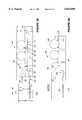
- FIG. 1ashows the front view of a strip 100 of the prior art, which is designed to form a 27 ⁇ 27 mm PBGA package.
- FIG. 1bshows the back view of strip 100 of FIG. 1a.
- FIG. 1cshows a solder ball 120 cracking under shear stresses on both ends of the solder ball.
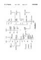
- FIG. 2ashows the top view of strip 200, which is designed for a 27 ⁇ 27 mm TGA package.
- FIG. 2bshows the bottom view of strip 200 of FIG. 2a.
- FIG. 2cshows a side view of strip 200 of FIG. 2a.
- FIG. 3ashows a package 300 using a stamped stiffener singulated out of a strip similar to strip 200 shown in FIGS. 2a-2c above.
- FIG. 3bshows a TGA package 350 using a stiffener having a cavity formed by an etching process.
- FIG. 4shows an assembly process 400 for assembling a TGA package of the present invention.
- FIG. 5shows the bottom side of a metal strip 500 after a TAB tape adhesion step.
- FIG. 6shows the bottom side of metal strip 500 after a solder reflow step.
- FIG. 7ashows a package 700 using a two-metal polyimide tape, in accordance with the present invention.
- FIG. 7bshows signal layer 713 of polyimide tape 710, which is designed the for a 352 pin TGA.
- the tapehas two metal layers.
- FIG. 8ashown another TGA package 800 of the present invention, which includes an elastomeric layer 802.
- FIG. 8bshows how TGA package 800 allows the solder balls of TGA package 800 to withstand a larger shear stress before fatigue cracking can occur.
- the present inventionprovides a novel TGA package using equipment, tools and established processes similar to those used in the BPGA packaging industry.
- like elements in the accompanying figuresare provided like reference numerals.
- FIGS. 1a and 1bshows respectively the front and back views of a multilayer printed circuit board (PCB) strip 100 of the prior art, which is designed for forming six 27 ⁇ 27 mm stiffeners for six PBGA packages.
- PCB strip 100is provided tooling holes 101-1 to 101-14 to facilitate automated handling by machines.
- three fiduciary marks 102-1 to 102-3are provided to assist alignment during the package assembly process.
- Tooling holes 101-1 to 101-14 and fiduciary marks 102-1 to 102-3are positioned in the area 104, which is outside of areas 103-1 to 103-6 from which the six packages are to be formed.
- Area 104is discarded at a subsequent step of singulation, during which areas 103-1 to 103-6 are severed for further processing into individual packages. Oval through holes 104-1 to 104-7 and 105-1 to 105-12 are provided to assist singulation. Of course, depending upon the size and pin-count of the PBGA package, the design and construction of PCB strip 100 vary.
- the present inventionallows stiffeners of TGA type packages to be formed from a strip similar to PCB strip 100 of FIGS 1a and 1b discussed above.
- a stripis illustrated by strip 200 shown in FIGS. 2a, 2b and 2c.
- FIGS. 2a, 2b and 2cshow, respectively, the top, bottom and side views of strip 200, which is designed for six 27 mm ⁇ 27 mm TGA packages.
- strip 200is a 0.65 mm thick 400 mm ⁇ 40 mm metallic strip.
- Strip 200can be formed from a thermally conductive material, such as copper or aluminum.
- a stiffener formed out of strip 200serves also as a heat spreader.
- Strip 200can also be formed out of plastic using an injection molding technique. The advantage of a plastic strip is the significant cost reduction that can be realized. However, the thermal and electrical performances of a package using a stiffener singulated from a plastic strip are poor relative to those packages singulated from a metal strip. Of course, strip 200 can also be made out of ceramic.
- Tooling holes 201-1 to 201-14are provided in substantially the same manner as tooling holes 101-1 to 101-14, as discussed above with respect to strip 100.
- the top surface of strip 200is substantially flat.
- This top surfacecan be plated with a metal, such as nickel, chromium or solder to provide a clean surface for attaching an external heatsink.
- this surfacecan be left bare, i.e. without plating, or can be oxidized to form a black oxide, in the case of a copper or an aluminum strip.
- the bottom surface (FIG. 2b), on which the polyimide tape is to be attached,can be left exposed or plated with nickel, chromium, palladium, silver or gold.
- a black oxide formed on a copper or aluminum stripwould also improve tape adhesion to a stiffener formed out of strip 200.
- the bottom surface of strip 200is shown in FIG. 2b.
- On the bottom side of strip 200is formed, using either etching or stamping, six 12 mm ⁇ 12 mm equally spaced cavities 203-1 to 203-6. In this embodiment, each cavity is 0.25 mm deep.
- Each of cavities 203-1 to 203-6provides a recessed area in which the semiconductor die is subsequently attached.
- the bottom side of strip 200is a flat surface. Alternately, however, the bottom side of strip 200 can also be stamped to form cavities 203-1 to 203-6, pushing out, 0.25 mm to 0.5 mm from the front surface, an area substantially corresponding in size to each cavity.
- cavities 203-1 to 203-6are primarily determined by the thickness of the semiconductor die each cavity is to hold.
- cavities 203-1 to 203-6can be eliminated to reduce both the material and the processing costs of the stiffener.
- a ring 202is plated on the bottom side (FIG. 2b) of strip 200, around the periphery of each of cavities 203-1 to 203-6.
- Plated ring 202is used to allow ground bonds to be attached to the stiffener.
- ring 202can be plated with a metal suitable for wire bonding, such as gold, silver, palladium, aluminum and other suitable metals.
- a solder wettable platinglike gold, silver or palladium is desirable.
- strip 200can be also designed to include multiple rows of stiffeners. In processing, multiple rows of stiffeners allow a higher throughput and better material utilization. The choice between a single-row strip or a multiple-row strip to be used in a particular design is determined by the process capabilities of the automated assembly equipment.
- FIG. 3ashows package 300 using a stiffener singulated out of a strip similar to strip 200 shown in FIGS. 2a-2c above.
- stiffener 301is a stiffener formed out of a flat metal strip, or metal laminate, of substantially uniform thickness (approximately 0.007 inches).
- a cavity 302is formed by a stamping process, which is less costly than forming such a cavity using an etching process. The stamping process is also more appropriate for the thinner TGA packages.
- the top surface of stiffener 301has a raised surface (approximately, 0.005 inches high) corresponding in position to cavity 302 formed on the bottom side of the carrier strip.
- semiconductor die 303(approximately 0.011 inches thick) is attached to the bottom of cavity 302 by epoxy film 304.
- epoxy film 304is approximately 0.001 inches thick.
- a thin epoxy layer 311attaches a polyimide tape 310 to stiffener 301.
- Bonding pad 307is connected to corresponding bonding pads on semiconductor die 303 by bond wires, such as bond wire 312. Ground bonds can be made between semiconductor die 303 and stiffener 301 at the plated ring (discussed above) around the periphery of cavity 302 using bond wires, such as bond wire 313. Through openings on the bottom surface of polyimide film 310, solder balls 308 contact metal traces 309 electrically. Cavity 302 and semiconductor die 303 are encapsulated in a thin encapsulation 305. As shown in FIG. 3a, the bottom surface of encapsulation 305 recessed at approximately 0.01 inches from the contact surface of the solder balls. In this embodiment, the thickness of encapsulation 305, as measured from the top surface of stiffener 301 to the bottom surface of encapsulation 305 is approximately 0.03 inches.
- FIG. 3bshows a TGA package 350 of the present invention using a stiffener in which the cavity is formed by an etching process.
- cavity 352is formed in stiffener 352 from etching a 0.012 inches thick metal strip.
- cavity 352is 0.005 inches deep.
- stiffener 351has a substantially flat top surface and is thicker at the peripheral area. An etched stiffener allows a heat dissipation higher than that of a stamped stiffener.
- thermoset or thermoplastic epoxy glueapproximately 1 mil thick
- a suitable thermoset adhesiveis the 3 Pm adhesive manufactured by Sheldahl Co.
- a suitable thermoplastic adhesiveis the acrylic tape F-9460PC, manufactured by 3M Co. Even though these thermoset or thermoplastic adhesives may soften during a solder ball reflow step, such as solder ball reflow step 405 described below, these adhesives can withstand, without damage, the short duration of higher temperature in step 405, which lasts less than a minute.
- the curing temperature of the thermoset epoxy glueis approximately 215° C.
- the tape frames on the tapeare then singulated.
- the singulated tape framesare attached to the carrier strip of the type described above (i.e. metal strips 300 and 305).
- each tape frameis vacuum-held by a cylindrical fixture which aligns the tape frame to the tooling holes of the metal strip.
- the cylindrical fixturehas a curved surface which is rocked against the metal strip to prevent any air bubbles to be trapped between the strip and the tape frame, as the tape frame is released onto the metal strip.
- the glueis then set on the metal strip under high heat (170° C.) and pressure.
- a metal polyimide tapehaving a melting point above 400° C. is used.
- FIG. 5shows the bottom view of TGA strip 500 on which six singulated tape frames are attached.
- Each tape frameincludes a cavity area 501 and a tape frame area 502.
- tape framescan be tiled on the tape with minimal waste between frames.
- maximum tape utilization without wastecan be achieved.
- tape cost in a TGA packagecan exceed 50% of the total package cost.
- 38%-50% of the tape costcan be saved under the present invention.
- the tape shown in FIG. 5will remain in the TGA package for the remainder of the assembly process.
- solder ballsare selected based on the criterion that the solder balls should not melt under the die attach and wire bonding steps (i.e. steps 409-411 described below) of the process. Since the die attach epoxy is cured at 170° C. and wire bonding is performed at 170° C. or lower temperature, as described below, both eutectic solder balls (e.g.
- a solder ball reflow stepat step 406 fixes the solder balls onto the tape frame using a reflow procedure, which is performed at 220° C. for eutectic solder balls.
- the solder balls of the present inventionare attached to a tape frame adhered to a metal strip, rather than a PCB.
- high temperature solder ballscan be used for a TGA package of the present invention. Consequently, unlike a PBGA package, a TGA package of the present invention using high temperature solder balls does not fail under solder ball fatigue.
- high temperature solder ballsare enabled by the fact that their solder reflow temperature of 300° C. in high temperature solder balls is lower than the polyimide critical temperature (over 400° C.) and that the reflow time is short enough not to cause any damage to the tape epoxy adhesive.
- a cleaning step, step 407,uses a conventional cleaning fluid to remove any excess solder flux from the bottom surface of the metal strip.
- FIG. 6shows strip 500 after step 407.
- solder balls 502are attached to a tape frame on strip 500.
- FIG. 6shows ring 504 around the periphery of cavity 501 coated for ground bonding.
- the ability to assemble the package and to take yield loss prior to die assemblyprovide a higher die assembly yield and a lower assembly cost.
- the TGA package of the present inventioncan be used for applications where access, before encapsulation, to the die is desired for such purposes as device debugging or device programming.
- a semiconductor dieis bonded by a uniform thin film (e.g. 1 mil) of silver epoxy to the bottom of each cavity on the carrier strip.
- the semiconductor dieis obtained conventionally by dicing a wafer using a wafer saw.
- a curing period (i.e. step 410) after die-attach step 409is provided, as appropriate, according to the requirements of the epoxy used.
- gold bonding wiresare then used to connect bond pads on the semiconductor die and either the bonding pads on the tape or, in the case of ground bonds, the ring at the periphery of each cavity. Because a low temperature PCB is not involved, wire-bonding temperature up to 170° C. can be tolerated. Wire bonding temperature 170 C. is lower than the solder ball melting temperature 183° C., for eutectic solder balls, or the material critical temperatures of the tape epoxy (215° C.) and the polyimide tape (over 400° C.).
- the metal stripincluding the semiconductor dies, the tape frames and the bond wires, are then encapsulated and cured, exposing only 0.01 inches of the solder balls.
- the six packages on the metal stripare then singulated and packed in containers for shipping, at steps 414 and 415 respectively.
- a TGA package using a two-metal tapei.e. a polyimide tape including two insulated layers of metal traces
- a packagecan also be formed from the metal strip, such as strip 200 above.
- the strip design, construction and package assembly processare substantially the same as those described above.
- FIG. 7ashows a TGA package 700 using a two-metal polyimide tape, in accordance with the present invention.
- TGA package 700uses a two-metal polyimide tape 710, which has a power/ground layer 712, in addition to a signal trace layer 713. As shown in FIG.
- tape 710has a solder mask layer which allows selective connections of the power/ground layer 712 to be made to stiffener 701.
- TGA package 700has three metal layers at its disposal: (i) signal trace layer 713 for signal routing; (ii) power/ground layer 712 for power connections; and (iii) stiffener 701, serving as a ground plane.
- the connections to the semiconductor dieare done via wire bonds. As shown in FIG.
- stiffener 701is 0.025 inches thick, having a 0.015 inches etched cavity 702.
- TGA package 700can provide high electrical performance up to 500 Mhz. This advantage is significant, since such performance is achieved in a cavity-down PBGA package or a ceramic BGA (CBGA) package only by using a multilayer substrate with three tiers, i.e. at significantly higher cost and larger electrical parasitic impedances. The superior electrical performance is achieved in the present invention through low-inductance power and ground connections and controlled impedance signal traces.
- FIG. 7bshows signal layer 713 of polyimide tape 710, which is designed for a 352 pin TGA.
- Solder ball padssuch as solder ball pad 755, are provided at the tape frame for connection to a mother board. Special solder ball pads, such as pad 751, are each connected through a via to the power/ground plane 712. Signal traces, such as trace 752 are coupled to wire bonding pads, such as wire bonding pad 752, close to cavity 702. Low inductance power and ground connections to signal trace layer 713 is achieved by having vias, such as via 753, located as closely as possible to the edge of cavity 702, hence as closely as possible to the semiconductor die.
- FIG. 8ashows another TGA package 800 of the present invention, which includes an elastomeric layer 802.
- stiffener 801is similar to stiffener 701 of FIG. 7a, with an additional 0.005 inches recess 804 etched out of the stiffener.
- recess 804is provided a flexible elastomeric layer 802 between tape frame 710 and stiffener 801.
- elastomeric layer 802is attached with adhesive layers 803, on one side, to the stiffener 801 and, on the other side, to polyimide tape 701. Both layers of adhesive layers 803 can be implemented by the same tape epoxy, such as tape epoxy 311 described above.
- Elastomeric layer 802can be chosen from rather dense elastomers, such as silicone or viton type materials.
- FIG. 8bshows how TGA package 800 allows the solder balls of TGA package 800 to withstand a larger shear stress before fatigue cracking can occur.
- the deformation of elastomeric layer 802 under solder ball 308 due to "rocking"is reduced, since elastomeric layer 802 under polyimide tape 710 deforms, such that solder ball 308 can tilt in the direction of the relative movement of TGA package 800. Consequently, a fraction of the shear stress at TGA package 800 is relieved. Hence, fatigue cracking can then only occur at a greater level of shear stress at end 826 attached to motherboard 122.
Landscapes
- Engineering & Computer Science (AREA)
- Computer Hardware Design (AREA)
- Microelectronics & Electronic Packaging (AREA)
- Power Engineering (AREA)
- Physics & Mathematics (AREA)
- Condensed Matter Physics & Semiconductors (AREA)
- General Physics & Mathematics (AREA)
- Geometry (AREA)
- Wire Bonding (AREA)
Abstract
Description
Claims (9)
Priority Applications (1)
| Application Number | Priority Date | Filing Date | Title |
|---|---|---|---|
| US08/585,134US5843808A (en) | 1996-01-11 | 1996-01-11 | Structure and method for automated assembly of a tab grid array package |
Applications Claiming Priority (1)
| Application Number | Priority Date | Filing Date | Title |
|---|---|---|---|
| US08/585,134US5843808A (en) | 1996-01-11 | 1996-01-11 | Structure and method for automated assembly of a tab grid array package |
Publications (1)
| Publication Number | Publication Date |
|---|---|
| US5843808Atrue US5843808A (en) | 1998-12-01 |
Family
ID=24340176
Family Applications (1)
| Application Number | Title | Priority Date | Filing Date |
|---|---|---|---|
| US08/585,134Expired - LifetimeUS5843808A (en) | 1996-01-11 | 1996-01-11 | Structure and method for automated assembly of a tab grid array package |
Country Status (1)
| Country | Link |
|---|---|
| US (1) | US5843808A (en) |
Cited By (102)
| Publication number | Priority date | Publication date | Assignee | Title |
|---|---|---|---|---|
| US6033937A (en)* | 1997-12-23 | 2000-03-07 | Vlsi Technology, Inc. | Si O2 wire bond insulation in semiconductor assemblies |
| US6040633A (en)* | 1997-12-23 | 2000-03-21 | Vlsi Technology, Inc. | Oxide wire bond insulation in semiconductor assemblies |
| US6194250B1 (en)* | 1998-09-14 | 2001-02-27 | Motorola, Inc. | Low-profile microelectronic package |
| US6198163B1 (en)* | 1999-10-18 | 2001-03-06 | Amkor Technology, Inc. | Thin leadframe-type semiconductor package having heat sink with recess and exposed surface |
| US6242933B1 (en) | 1999-10-04 | 2001-06-05 | St Assembly Test Services | Device probe socket forming part of a test head, interfacing between test head and a probe handler, used for device strip testing |
| US6253675B1 (en) | 1999-06-29 | 2001-07-03 | Carl P. Mayer | Solder paste stenciling apparatus and method of use for rework |
| US6284572B1 (en) | 2000-08-14 | 2001-09-04 | St Assembly Test Services Pte Ltd. | Boat and assembly method for ball grid array packages |
| US6297078B1 (en)* | 1997-12-31 | 2001-10-02 | Intel Corporation | Integrated circuit package with bond wires at the corners of an integrated circuit |
| US6329713B1 (en)* | 1998-10-21 | 2001-12-11 | International Business Machines Corporation | Integrated circuit chip carrier assembly comprising a stiffener attached to a dielectric substrate |
| US6379982B1 (en)* | 2000-08-17 | 2002-04-30 | Micron Technology, Inc. | Wafer on wafer packaging and method of fabrication for full-wafer burn-in and testing |
| US6396130B1 (en) | 2001-09-14 | 2002-05-28 | Amkor Technology, Inc. | Semiconductor package having multiple dies with independently biased back surfaces |
| US20020079562A1 (en)* | 2000-12-22 | 2002-06-27 | Broadcom Corporation | Enhanced die-up ball grid array packages and method for making the same |
| US6429048B1 (en) | 2000-12-05 | 2002-08-06 | Asat Ltd. | Metal foil laminated IC package |
| US20030001151A1 (en)* | 2001-06-29 | 2003-01-02 | Intel Corporation | Discrete polymer memory array and method of making same |
| US20030001176A1 (en)* | 2001-06-29 | 2003-01-02 | Intel Corporation | Low-voltage and interface damage-free polymer memory device |
| US20030017627A1 (en)* | 2001-07-20 | 2003-01-23 | Intel Corporation | Stacked ferroelectric memory device and method of making same |
| US6524887B2 (en)* | 2001-07-20 | 2003-02-25 | Intel Corporation | Embedded recess in polymer memory package and method of making same |
| US20030057550A1 (en)* | 2000-12-22 | 2003-03-27 | Broadcom Corporation | Ball grid array package enhanced with a thermal and electrical connector |
| US6543127B1 (en) | 2000-07-11 | 2003-04-08 | St Assembly Test Service Ltd. | Coplanarity inspection at the singulation process |
| US6544812B1 (en) | 2000-11-06 | 2003-04-08 | St Assembly Test Service Ltd. | Single unit automated assembly of flex enhanced ball grid array packages |
| US6559536B1 (en) | 1999-12-13 | 2003-05-06 | Fujitsu Limited | Semiconductor device having a heat spreading plate |
| US6562661B2 (en) | 2000-02-24 | 2003-05-13 | Micron Technology, Inc. | Tape stiffener, semiconductor device component assemblies including same, and stereolithographic methods for fabricating same |
| US6564987B2 (en)* | 2000-11-16 | 2003-05-20 | Fujitsu Limited | Method, apparatus and computer readable medium for evaluating configuration of solder external terminals of a semiconductor device |
| US6576988B2 (en)* | 1999-08-30 | 2003-06-10 | Micron Technology, Inc. | Semiconductor package |
| US20030146503A1 (en)* | 2002-02-01 | 2003-08-07 | Broadcom Corporation | Ball grid array package with stepped stiffener layer |
| US20030146511A1 (en)* | 2002-02-01 | 2003-08-07 | Broadcom Corporation | Ball grid array package with multiple interposers |
| US20030146506A1 (en)* | 2002-02-01 | 2003-08-07 | Broadcom Corporation | Ball grid array package fabrication with IC die support structures |
| US20030178719A1 (en)* | 2002-03-22 | 2003-09-25 | Combs Edward G. | Enhanced thermal dissipation integrated circuit package and method of manufacturing enhanced thermal dissipation integrated circuit package |
| US6756251B2 (en) | 2001-08-21 | 2004-06-29 | Micron Technology, Inc. | Method of manufacturing microelectronic devices, including methods of underfilling microelectronic components through an underfill aperture |
| US6770513B1 (en)* | 1999-12-16 | 2004-08-03 | National Semiconductor Corporation | Thermally enhanced flip chip packaging arrangement |
| US6790710B2 (en) | 2002-01-31 | 2004-09-14 | Asat Limited | Method of manufacturing an integrated circuit package |
| US20040195685A1 (en)* | 2003-04-02 | 2004-10-07 | Stmicroelectronics, Inc. | System and method for venting pressure from an integrated circuit package sealed with a lid |
| US20040219713A1 (en)* | 2002-01-09 | 2004-11-04 | Micron Technology, Inc. | Elimination of RDL using tape base flip chip on flex for die stacking |
| US6853070B2 (en) | 2001-02-15 | 2005-02-08 | Broadcom Corporation | Die-down ball grid array package with die-attached heat spreader and method for making the same |
| US6858932B2 (en) | 2002-02-07 | 2005-02-22 | Freescale Semiconductor, Inc. | Packaged semiconductor device and method of formation |
| US20050051896A1 (en)* | 2003-07-30 | 2005-03-10 | Martin Reiss | Arrangement for improving module reliability |
| US6876553B2 (en) | 2002-03-21 | 2005-04-05 | Broadcom Corporation | Enhanced die-up ball grid array package with two substrates |
| US6879039B2 (en)* | 2001-12-18 | 2005-04-12 | Broadcom Corporation | Ball grid array package substrates and method of making the same |
| US6882042B2 (en) | 2000-12-01 | 2005-04-19 | Broadcom Corporation | Thermally and electrically enhanced ball grid array packaging |
| US6906414B2 (en)* | 2000-12-22 | 2005-06-14 | Broadcom Corporation | Ball grid array package with patterned stiffener layer |
| US6916682B2 (en) | 2001-11-08 | 2005-07-12 | Freescale Semiconductor, Inc. | Semiconductor package device for use with multiple integrated circuits in a stacked configuration and method of formation and testing |
| US20050269687A1 (en)* | 2002-11-08 | 2005-12-08 | Robert Forcier | Build-up structures with multi-angle vias for chip to chip interconnects and optical bussing |
| US6975035B2 (en) | 2002-03-04 | 2005-12-13 | Micron Technology, Inc. | Method and apparatus for dielectric filling of flip chip on interposer assembly |
| US6982485B1 (en)* | 2002-02-13 | 2006-01-03 | Amkor Technology, Inc. | Stacking structure for semiconductor chips and a semiconductor package using it |
| US6989593B2 (en) | 2000-12-22 | 2006-01-24 | Broadcom Corporation | Die-up ball grid array package with patterned stiffener opening |
| US20060055038A1 (en)* | 2004-09-10 | 2006-03-16 | Jinghui Mu | Tape ball grid array package with electromagnetic interference protection and method for fabricating the package |
| US7018853B1 (en) | 2001-07-20 | 2006-03-28 | Intel Corporation | Stepped structure for a multi-rank, stacked polymer memory device and method of making same |
| EP1657043A1 (en)* | 2004-11-02 | 2006-05-17 | Apic Yamada Corporation | Equipment and method for controlling encapsulating semiconductors with plastics |
| US7087460B2 (en) | 2002-03-04 | 2006-08-08 | Micron Technology, Inc. | Methods for assembly and packaging of flip chip configured dice with interposer |
| US7112520B2 (en) | 2002-03-04 | 2006-09-26 | Micron Technology, Inc. | Semiconductor die packages with recessed interconnecting structures and methods for assembling the same |
| US7115986B2 (en) | 2001-05-02 | 2006-10-03 | Micron Technology, Inc. | Flexible ball grid array chip scale packages |
| US7145225B2 (en) | 2002-03-04 | 2006-12-05 | Micron Technology, Inc. | Interposer configured to reduce the profiles of semiconductor device assemblies and packages including the same and methods |
| US7161237B2 (en) | 2002-03-04 | 2007-01-09 | Micron Technology, Inc. | Flip chip packaging using recessed interposer terminals |
| US7196415B2 (en) | 2002-03-22 | 2007-03-27 | Broadcom Corporation | Low voltage drop and high thermal performance ball grid array package |
| US7259457B2 (en) | 2001-05-07 | 2007-08-21 | Broadcom Corporation | Die-up ball grid array package including a substrate capable of mounting an integrated circuit die and method for making the same |
| US7320933B2 (en) | 2002-08-20 | 2008-01-22 | Micron Technology, Inc. | Double bumping of flexible substrate for first and second level interconnects |
| US7411281B2 (en) | 2004-06-21 | 2008-08-12 | Broadcom Corporation | Integrated circuit device package having both wire bond and flip-chip interconnections and method of making the same |
| US20080191367A1 (en)* | 2007-02-08 | 2008-08-14 | Stats Chippac, Ltd. | Semiconductor package wire bonding |
| US7432586B2 (en) | 2004-06-21 | 2008-10-07 | Broadcom Corporation | Apparatus and method for thermal and electromagnetic interference (EMI) shielding enhancement in die-up array packages |
| US20080273314A1 (en)* | 2007-05-04 | 2008-11-06 | Samsung Electronics Co., Ltd. | PCB having embedded IC and method for manufacturing the same |
| US7482686B2 (en) | 2004-06-21 | 2009-01-27 | Braodcom Corporation | Multipiece apparatus for thermal and electromagnetic interference (EMI) shielding enhancement in die-up array packages and method of making the same |
| US7550845B2 (en) | 2002-02-01 | 2009-06-23 | Broadcom Corporation | Ball grid array package with separated stiffener layer |
| US20090209064A1 (en)* | 2006-04-28 | 2009-08-20 | Somchai Nonahasitthichai | Lead frame land grid array |
| US20090267227A1 (en)* | 2008-04-24 | 2009-10-29 | Lockheed Martin Corporation | Plastic ball grid array ruggedization |
| US20100019374A1 (en)* | 2008-07-25 | 2010-01-28 | Stmicroelectronics, Inc. | Ball grid array package |
| US7786591B2 (en) | 2004-09-29 | 2010-08-31 | Broadcom Corporation | Die down ball grid array package |
| US7790512B1 (en) | 2007-11-06 | 2010-09-07 | Utac Thai Limited | Molded leadframe substrate semiconductor package |
| US20100230802A1 (en)* | 2009-03-12 | 2010-09-16 | Utac Thai Limited | Metallic solderability preservation coating on metal part of semiconductor package to prevent oxide |
| US20110018111A1 (en)* | 2009-07-23 | 2011-01-27 | Utac Thai Limited | Leadframe feature to minimize flip-chip semiconductor die collapse during flip-chip reflow |
| US7915718B2 (en) | 2002-03-04 | 2011-03-29 | Micron Technology, Inc. | Apparatus for flip-chip packaging providing testing capability |
| US8013437B1 (en) | 2006-09-26 | 2011-09-06 | Utac Thai Limited | Package with heat transfer |
| US8063470B1 (en) | 2008-05-22 | 2011-11-22 | Utac Thai Limited | Method and apparatus for no lead semiconductor package |
| US8125077B2 (en) | 2006-09-26 | 2012-02-28 | Utac Thai Limited | Package with heat transfer |
| US8183680B2 (en) | 2006-05-16 | 2012-05-22 | Broadcom Corporation | No-lead IC packages having integrated heat spreader for electromagnetic interference (EMI) shielding and thermal enhancement |
| US8368189B2 (en) | 2009-12-04 | 2013-02-05 | Utac Thai Limited | Auxiliary leadframe member for stabilizing the bond wire process |
| US8460970B1 (en) | 2006-04-28 | 2013-06-11 | Utac Thai Limited | Lead frame ball grid array with traces under die having interlocking features |
| US8461694B1 (en) | 2006-04-28 | 2013-06-11 | Utac Thai Limited | Lead frame ball grid array with traces under die having interlocking features |
| US8487451B2 (en) | 2006-04-28 | 2013-07-16 | Utac Thai Limited | Lead frame land grid array with routing connector trace under unit |
| US8492906B2 (en) | 2006-04-28 | 2013-07-23 | Utac Thai Limited | Lead frame ball grid array with traces under die |
| US20130256858A1 (en)* | 2012-03-28 | 2013-10-03 | Infineon Technologies North America Corp. | PCB Based RF-Power Package Window Frame |
| US8575732B2 (en) | 2010-03-11 | 2013-11-05 | Utac Thai Limited | Leadframe based multi terminal IC package |
| US20130301252A1 (en)* | 2012-04-13 | 2013-11-14 | Cree, Inc. | Gas cooled led lamp |
| US8871571B2 (en) | 2010-04-02 | 2014-10-28 | Utac Thai Limited | Apparatus for and methods of attaching heat slugs to package tops |
| US9000590B2 (en) | 2012-05-10 | 2015-04-07 | Utac Thai Limited | Protruding terminals with internal routing interconnections semiconductor device |
| US9006034B1 (en) | 2012-06-11 | 2015-04-14 | Utac Thai Limited | Post-mold for semiconductor package having exposed traces |
| US9082607B1 (en) | 2006-12-14 | 2015-07-14 | Utac Thai Limited | Molded leadframe substrate semiconductor package |
| US9355940B1 (en) | 2009-12-04 | 2016-05-31 | Utac Thai Limited | Auxiliary leadframe member for stabilizing the bond wire process |
| US9449905B2 (en) | 2012-05-10 | 2016-09-20 | Utac Thai Limited | Plated terminals with routing interconnections semiconductor device |
| US9629246B2 (en) | 2015-07-28 | 2017-04-18 | Infineon Technologies Ag | PCB based semiconductor package having integrated electrical functionality |
| US9651240B2 (en) | 2013-11-14 | 2017-05-16 | Cree, Inc. | LED lamp |
| US9761435B1 (en) | 2006-12-14 | 2017-09-12 | Utac Thai Limited | Flip chip cavity package |
| US9805955B1 (en) | 2015-11-10 | 2017-10-31 | UTAC Headquarters Pte. Ltd. | Semiconductor package with multiple molding routing layers and a method of manufacturing the same |
| US9810379B2 (en) | 2012-04-13 | 2017-11-07 | Cree, Inc. | LED lamp |
| US9947605B2 (en) | 2008-09-04 | 2018-04-17 | UTAC Headquarters Pte. Ltd. | Flip chip cavity package |
| US9951909B2 (en) | 2012-04-13 | 2018-04-24 | Cree, Inc. | LED lamp |
| US9997476B2 (en) | 2015-10-30 | 2018-06-12 | Infineon Technologies Ag | Multi-die package having different types of semiconductor dies attached to the same thermally conductive flange |
| US10225922B2 (en) | 2016-02-18 | 2019-03-05 | Cree, Inc. | PCB based semiconductor package with impedance matching network elements integrated therein |
| US10242934B1 (en) | 2014-05-07 | 2019-03-26 | Utac Headquarters Pte Ltd. | Semiconductor package with full plating on contact side surfaces and methods thereof |
| US10242953B1 (en) | 2015-05-27 | 2019-03-26 | Utac Headquarters PTE. Ltd | Semiconductor package with plated metal shielding and a method thereof |
| US10276477B1 (en) | 2016-05-20 | 2019-04-30 | UTAC Headquarters Pte. Ltd. | Semiconductor package with multiple stacked leadframes and a method of manufacturing the same |
| US10468399B2 (en) | 2015-03-31 | 2019-11-05 | Cree, Inc. | Multi-cavity package having single metal flange |
| USRE48489E1 (en) | 2012-04-13 | 2021-03-30 | Ideal Industries Lighting Llc | Gas cooled LED lamp |
Citations (5)
| Publication number | Priority date | Publication date | Assignee | Title |
|---|---|---|---|---|
| US5409865A (en)* | 1993-09-03 | 1995-04-25 | Advanced Semiconductor Assembly Technology | Process for assembling a TAB grid array package for an integrated circuit |
| US5420460A (en)* | 1993-08-05 | 1995-05-30 | Vlsi Technology, Inc. | Thin cavity down ball grid array package based on wirebond technology |
| US5474957A (en)* | 1994-05-09 | 1995-12-12 | Nec Corporation | Process of mounting tape automated bonded semiconductor chip on printed circuit board through bumps |
| US5482898A (en)* | 1993-04-12 | 1996-01-09 | Amkor Electronics, Inc. | Method for forming a semiconductor device having a thermal dissipator and electromagnetic shielding |
| US5556807A (en)* | 1992-02-18 | 1996-09-17 | Intel Corporation | Advance multilayer molded plastic package using mesic technology |
- 1996
- 1996-01-11USUS08/585,134patent/US5843808A/ennot_activeExpired - Lifetime
Patent Citations (5)
| Publication number | Priority date | Publication date | Assignee | Title |
|---|---|---|---|---|
| US5556807A (en)* | 1992-02-18 | 1996-09-17 | Intel Corporation | Advance multilayer molded plastic package using mesic technology |
| US5482898A (en)* | 1993-04-12 | 1996-01-09 | Amkor Electronics, Inc. | Method for forming a semiconductor device having a thermal dissipator and electromagnetic shielding |
| US5420460A (en)* | 1993-08-05 | 1995-05-30 | Vlsi Technology, Inc. | Thin cavity down ball grid array package based on wirebond technology |
| US5409865A (en)* | 1993-09-03 | 1995-04-25 | Advanced Semiconductor Assembly Technology | Process for assembling a TAB grid array package for an integrated circuit |
| US5474957A (en)* | 1994-05-09 | 1995-12-12 | Nec Corporation | Process of mounting tape automated bonded semiconductor chip on printed circuit board through bumps |
Non-Patent Citations (4)
| Title |
|---|
| "An Overview of TBGA Bond and Assembly Operations", Michael Bernier, '95 Flip Chip, BGA, TAB & AP Symposium, 1995 Semiconductor Technology Center, Inc. no month. |
| "Design of a Low Cost Wire Bond Tape Ball Grid Array (TBGA) Package", R.D. Schueller and A. P. Plepys, Surface Mount International Proceedings, Aug. 30, 1995, pp. 261-269. |
| An Overview of TBGA Bond and Assembly Operations , Michael Bernier, 95 Flip Chip, BGA, TAB & AP Symposium, 1995 Semiconductor Technology Center, Inc. no month.* |
| Design of a Low Cost Wire Bond Tape Ball Grid Array (TBGA) Package , R.D. Schueller and A. P. Plepys, Surface Mount International Proceedings, Aug. 30, 1995, pp. 261 269.* |
Cited By (218)
| Publication number | Priority date | Publication date | Assignee | Title |
|---|---|---|---|---|
| US6040633A (en)* | 1997-12-23 | 2000-03-21 | Vlsi Technology, Inc. | Oxide wire bond insulation in semiconductor assemblies |
| US6046075A (en)* | 1997-12-23 | 2000-04-04 | Vlsi Technology, Inc. | Oxide wire bond insulation in semiconductor assemblies |
| US6033937A (en)* | 1997-12-23 | 2000-03-07 | Vlsi Technology, Inc. | Si O2 wire bond insulation in semiconductor assemblies |
| US6297078B1 (en)* | 1997-12-31 | 2001-10-02 | Intel Corporation | Integrated circuit package with bond wires at the corners of an integrated circuit |
| US6420651B1 (en) | 1997-12-31 | 2002-07-16 | Intel Corporation | Integrated circuit package with bond wires at the corners of an integrated circuit |
| US6194250B1 (en)* | 1998-09-14 | 2001-02-27 | Motorola, Inc. | Low-profile microelectronic package |
| US6329713B1 (en)* | 1998-10-21 | 2001-12-11 | International Business Machines Corporation | Integrated circuit chip carrier assembly comprising a stiffener attached to a dielectric substrate |
| US6253675B1 (en) | 1999-06-29 | 2001-07-03 | Carl P. Mayer | Solder paste stenciling apparatus and method of use for rework |
| US6576988B2 (en)* | 1999-08-30 | 2003-06-10 | Micron Technology, Inc. | Semiconductor package |
| US6242933B1 (en) | 1999-10-04 | 2001-06-05 | St Assembly Test Services | Device probe socket forming part of a test head, interfacing between test head and a probe handler, used for device strip testing |
| US6198163B1 (en)* | 1999-10-18 | 2001-03-06 | Amkor Technology, Inc. | Thin leadframe-type semiconductor package having heat sink with recess and exposed surface |
| US6559536B1 (en) | 1999-12-13 | 2003-05-06 | Fujitsu Limited | Semiconductor device having a heat spreading plate |
| US6796024B2 (en) | 1999-12-13 | 2004-09-28 | Fujitsu Limited | Method for making semiconductor device |
| US6770513B1 (en)* | 1999-12-16 | 2004-08-03 | National Semiconductor Corporation | Thermally enhanced flip chip packaging arrangement |
| US6740962B1 (en) | 2000-02-24 | 2004-05-25 | Micron Technology, Inc. | Tape stiffener, semiconductor device component assemblies including same, and stereolithographic methods for fabricating same |
| US6900078B2 (en) | 2000-02-24 | 2005-05-31 | Micron Technology, Inc. | Tape stiffener, semiconductor device component assemblies including same, and stereolithographic methods for fabricating same |
| US7189600B2 (en) | 2000-02-24 | 2007-03-13 | Micron Technology, Inc. | Methods for fabricating stiffeners for flexible substrates |
| US20030176021A1 (en)* | 2000-02-24 | 2003-09-18 | Grigg Ford B. | Tape stiffener, semiconductor device component assemblies including same, and stereolithographic methods for fabricating same |
| US20060121649A1 (en)* | 2000-02-24 | 2006-06-08 | Grigg Ford B | Methods for fabricating stiffeners for flexible substrates |
| US20070172992A1 (en)* | 2000-02-24 | 2007-07-26 | Grigg Ford B | Methods for fabricating stiffeners for flexible substrates |
| US20040224442A1 (en)* | 2000-02-24 | 2004-11-11 | Grigg Ford B. | Tape stiffener, semiconductor device component assemblies including same, and stereolithographic methods for fabricating same |
| US7029954B2 (en) | 2000-02-24 | 2006-04-18 | Micron Technology, Inc. | Tape stiffener, semiconductor device component assemblies including same, and stereolithographic methods for fabricating same |
| US6746899B2 (en) | 2000-02-24 | 2004-06-08 | Micron Technology, Inc. | Tape stiffener, semiconductor device component assemblies including same, and stereolithographic methods for fabricating same |
| US20040212062A1 (en)* | 2000-02-24 | 2004-10-28 | Grigg Ford B. | Tape stiffener and semiconductor device component assemblies including same |
| US20040142507A1 (en)* | 2000-02-24 | 2004-07-22 | Grigg Ford B. | Tape stiffener, semiconductor device component assemblies including same, and stereolithographic methods for fabricating same |
| US6562661B2 (en) | 2000-02-24 | 2003-05-13 | Micron Technology, Inc. | Tape stiffener, semiconductor device component assemblies including same, and stereolithographic methods for fabricating same |
| US6543127B1 (en) | 2000-07-11 | 2003-04-08 | St Assembly Test Service Ltd. | Coplanarity inspection at the singulation process |
| SG87201A1 (en)* | 2000-08-14 | 2002-03-19 | St Assembly Test Services Ltd | Boat and assembly method for ball grid array packages |
| US6284572B1 (en) | 2000-08-14 | 2001-09-04 | St Assembly Test Services Pte Ltd. | Boat and assembly method for ball grid array packages |
| US6359336B1 (en) | 2000-08-14 | 2002-03-19 | St Assembly Test Services Pte Ltd | Boat and assembly method for ball grid array packages |
| US6790684B2 (en) | 2000-08-17 | 2004-09-14 | Micron Technology, Inc. | Wafer on wafer packaging and method of fabrication for full-wafer burn-in and testing |
| US20020110953A1 (en)* | 2000-08-17 | 2002-08-15 | Ahn Kie Y. | Wafer on wafer packaging and method of fabrication for full-wafer burn-in and testing |
| US6653208B2 (en) | 2000-08-17 | 2003-11-25 | Micron Technology, Inc. | Wafer on wafer packaging and method of fabrication for full-wafer burn-in and testing |
| US6379982B1 (en)* | 2000-08-17 | 2002-04-30 | Micron Technology, Inc. | Wafer on wafer packaging and method of fabrication for full-wafer burn-in and testing |
| US6544812B1 (en) | 2000-11-06 | 2003-04-08 | St Assembly Test Service Ltd. | Single unit automated assembly of flex enhanced ball grid array packages |
| US6759752B2 (en) | 2000-11-06 | 2004-07-06 | St Assembly Test Services Ltd. | Single unit automated assembly of flex enhanced ball grid array packages |
| US6564987B2 (en)* | 2000-11-16 | 2003-05-20 | Fujitsu Limited | Method, apparatus and computer readable medium for evaluating configuration of solder external terminals of a semiconductor device |
| US8039949B2 (en) | 2000-12-01 | 2011-10-18 | Broadcom Corporation | Ball grid array package having one or more stiffeners |
| US8686558B2 (en) | 2000-12-01 | 2014-04-01 | Broadcom Corporation | Thermally and electrically enhanced ball grid array package |
| US6882042B2 (en) | 2000-12-01 | 2005-04-19 | Broadcom Corporation | Thermally and electrically enhanced ball grid array packaging |
| US7629681B2 (en) | 2000-12-01 | 2009-12-08 | Broadcom Corporation | Ball grid array package with patterned stiffener surface and method of assembling the same |
| US6429048B1 (en) | 2000-12-05 | 2002-08-06 | Asat Ltd. | Metal foil laminated IC package |
| US7132744B2 (en) | 2000-12-22 | 2006-11-07 | Broadcom Corporation | Enhanced die-up ball grid array packages and method for making the same |
| US20020079562A1 (en)* | 2000-12-22 | 2002-06-27 | Broadcom Corporation | Enhanced die-up ball grid array packages and method for making the same |
| US7579217B2 (en) | 2000-12-22 | 2009-08-25 | Broadcom Corporation | Methods of making a die-up ball grid array package with printed circuit board attachable heat spreader |
| US7893546B2 (en) | 2000-12-22 | 2011-02-22 | Broadcom Corporation | Ball grid array package enhanced with a thermal and electrical connector |
| US7859101B2 (en) | 2000-12-22 | 2010-12-28 | Broadcom Corporation | Die-up ball grid array package with die-attached heat spreader |
| US20030057550A1 (en)* | 2000-12-22 | 2003-03-27 | Broadcom Corporation | Ball grid array package enhanced with a thermal and electrical connector |
| US7038312B2 (en) | 2000-12-22 | 2006-05-02 | Broadcom Corporation | Die-up ball grid array package with attached stiffener ring |
| US7005737B2 (en) | 2000-12-22 | 2006-02-28 | Broadcom Corporation | Die-up ball grid array package with enhanced stiffener |
| US7161239B2 (en) | 2000-12-22 | 2007-01-09 | Broadcom Corporation | Ball grid array package enhanced with a thermal and electrical connector |
| US6989593B2 (en) | 2000-12-22 | 2006-01-24 | Broadcom Corporation | Die-up ball grid array package with patterned stiffener opening |
| US7462933B2 (en) | 2000-12-22 | 2008-12-09 | Broadcom Corporation | Ball grid array package enhanced with a thermal and electrical connector |
| US6906414B2 (en)* | 2000-12-22 | 2005-06-14 | Broadcom Corporation | Ball grid array package with patterned stiffener layer |
| US8310067B2 (en) | 2000-12-22 | 2012-11-13 | Broadcom Corporation | Ball grid array package enhanced with a thermal and electrical connector |
| US7102225B2 (en) | 2000-12-22 | 2006-09-05 | Broadcom Corporation | Die-up ball grid array package with printed circuit board attachable heat spreader |
| US7227256B2 (en) | 2000-12-22 | 2007-06-05 | Broadcom Corporation | Die-up ball grid array package with printed circuit board attachable heat spreader |
| US7202559B2 (en) | 2000-12-22 | 2007-04-10 | Broadcom Corporation | Method of assembling a ball grid array package with patterned stiffener layer |
| US7402906B2 (en) | 2001-02-15 | 2008-07-22 | Broadcom Corporation | Enhanced die-down ball grid array and method for making the same |
| US6853070B2 (en) | 2001-02-15 | 2005-02-08 | Broadcom Corporation | Die-down ball grid array package with die-attached heat spreader and method for making the same |
| US7115986B2 (en) | 2001-05-02 | 2006-10-03 | Micron Technology, Inc. | Flexible ball grid array chip scale packages |
| US7259457B2 (en) | 2001-05-07 | 2007-08-21 | Broadcom Corporation | Die-up ball grid array package including a substrate capable of mounting an integrated circuit die and method for making the same |
| US7259448B2 (en) | 2001-05-07 | 2007-08-21 | Broadcom Corporation | Die-up ball grid array package with a heat spreader and method for making the same |
| US20030001176A1 (en)* | 2001-06-29 | 2003-01-02 | Intel Corporation | Low-voltage and interface damage-free polymer memory device |
| US6858862B2 (en) | 2001-06-29 | 2005-02-22 | Intel Corporation | Discrete polymer memory array and method of making same |
| US20030001151A1 (en)* | 2001-06-29 | 2003-01-02 | Intel Corporation | Discrete polymer memory array and method of making same |
| US6756620B2 (en) | 2001-06-29 | 2004-06-29 | Intel Corporation | Low-voltage and interface damage-free polymer memory device |
| US20030017627A1 (en)* | 2001-07-20 | 2003-01-23 | Intel Corporation | Stacked ferroelectric memory device and method of making same |
| US7018853B1 (en) | 2001-07-20 | 2006-03-28 | Intel Corporation | Stepped structure for a multi-rank, stacked polymer memory device and method of making same |
| US6524887B2 (en)* | 2001-07-20 | 2003-02-25 | Intel Corporation | Embedded recess in polymer memory package and method of making same |
| US6960479B2 (en) | 2001-07-20 | 2005-11-01 | Intel Corporation | Stacked ferroelectric memory device and method of making same |
| US6756251B2 (en) | 2001-08-21 | 2004-06-29 | Micron Technology, Inc. | Method of manufacturing microelectronic devices, including methods of underfilling microelectronic components through an underfill aperture |
| US7087994B2 (en) | 2001-08-21 | 2006-08-08 | Micron Technology, Inc. | Microelectronic devices including underfill apertures |
| US6396130B1 (en) | 2001-09-14 | 2002-05-28 | Amkor Technology, Inc. | Semiconductor package having multiple dies with independently biased back surfaces |
| US6916682B2 (en) | 2001-11-08 | 2005-07-12 | Freescale Semiconductor, Inc. | Semiconductor package device for use with multiple integrated circuits in a stacked configuration and method of formation and testing |
| US7405145B2 (en) | 2001-12-18 | 2008-07-29 | Broadcom Corporation | Ball grid array package substrates with a modified central opening and method for making the same |
| US6879039B2 (en)* | 2001-12-18 | 2005-04-12 | Broadcom Corporation | Ball grid array package substrates and method of making the same |
| US7189593B2 (en) | 2002-01-09 | 2007-03-13 | Micron Technology, Inc. | Elimination of RDL using tape base flip chip on flex for die stacking |
| US20040219713A1 (en)* | 2002-01-09 | 2004-11-04 | Micron Technology, Inc. | Elimination of RDL using tape base flip chip on flex for die stacking |
| US8441113B2 (en) | 2002-01-09 | 2013-05-14 | Micron Technology, Inc. | Elimination of RDL using tape base flip chip on flex for die stacking |
| US8125065B2 (en) | 2002-01-09 | 2012-02-28 | Micron Technology, Inc. | Elimination of RDL using tape base flip chip on flex for die stacking |
| US7129584B2 (en) | 2002-01-09 | 2006-10-31 | Micron Technology, Inc. | Elimination of RDL using tape base flip chip on flex for die stacking |
| US6790710B2 (en) | 2002-01-31 | 2004-09-14 | Asat Limited | Method of manufacturing an integrated circuit package |
| US7078806B2 (en) | 2002-02-01 | 2006-07-18 | Broadcom Corporation | IC die support structures for ball grid array package fabrication |
| US7550845B2 (en) | 2002-02-01 | 2009-06-23 | Broadcom Corporation | Ball grid array package with separated stiffener layer |
| US20030146506A1 (en)* | 2002-02-01 | 2003-08-07 | Broadcom Corporation | Ball grid array package fabrication with IC die support structures |
| US20030146511A1 (en)* | 2002-02-01 | 2003-08-07 | Broadcom Corporation | Ball grid array package with multiple interposers |
| US20030146503A1 (en)* | 2002-02-01 | 2003-08-07 | Broadcom Corporation | Ball grid array package with stepped stiffener layer |
| US6825108B2 (en) | 2002-02-01 | 2004-11-30 | Broadcom Corporation | Ball grid array package fabrication with IC die support structures |
| US7241645B2 (en) | 2002-02-01 | 2007-07-10 | Broadcom Corporation | Method for assembling a ball grid array package with multiple interposers |
| US6861750B2 (en) | 2002-02-01 | 2005-03-01 | Broadcom Corporation | Ball grid array package with multiple interposers |
| US7245500B2 (en) | 2002-02-01 | 2007-07-17 | Broadcom Corporation | Ball grid array package with stepped stiffener layer |
| US6858932B2 (en) | 2002-02-07 | 2005-02-22 | Freescale Semiconductor, Inc. | Packaged semiconductor device and method of formation |
| US6982485B1 (en)* | 2002-02-13 | 2006-01-03 | Amkor Technology, Inc. | Stacking structure for semiconductor chips and a semiconductor package using it |
| US6975035B2 (en) | 2002-03-04 | 2005-12-13 | Micron Technology, Inc. | Method and apparatus for dielectric filling of flip chip on interposer assembly |
| US7534660B2 (en) | 2002-03-04 | 2009-05-19 | Micron Technology, Inc. | Methods for assembly and packaging of flip chip configured dice with interposer |
| US7087460B2 (en) | 2002-03-04 | 2006-08-08 | Micron Technology, Inc. | Methods for assembly and packaging of flip chip configured dice with interposer |
| US7230330B2 (en) | 2002-03-04 | 2007-06-12 | Micron Technology, Inc. | Semiconductor die packages with recessed interconnecting structures |
| US7112520B2 (en) | 2002-03-04 | 2006-09-26 | Micron Technology, Inc. | Semiconductor die packages with recessed interconnecting structures and methods for assembling the same |
| US7902648B2 (en) | 2002-03-04 | 2011-03-08 | Micron Technology, Inc. | Interposer configured to reduce the profiles of semiconductor device assemblies, packages including the same, and methods |
| US7915718B2 (en) | 2002-03-04 | 2011-03-29 | Micron Technology, Inc. | Apparatus for flip-chip packaging providing testing capability |
| US7569473B2 (en) | 2002-03-04 | 2009-08-04 | Micron Technology, Inc. | Methods of forming semiconductor assemblies |
| US7122907B2 (en) | 2002-03-04 | 2006-10-17 | Micron Technology, Inc. | Interposer substrate and wafer scale interposer substrate member for use with flip-chip configured semiconductor dice |
| US7531906B2 (en) | 2002-03-04 | 2009-05-12 | Micron Technology, Inc. | Flip chip packaging using recessed interposer terminals |
| US20110204499A1 (en)* | 2002-03-04 | 2011-08-25 | Micron Technology, Inc. | Semiconductor device assemblies |
| US7348215B2 (en) | 2002-03-04 | 2008-03-25 | Micron Technology, Inc. | Methods for assembly and packaging of flip chip configured dice with interposer |
| US7145225B2 (en) | 2002-03-04 | 2006-12-05 | Micron Technology, Inc. | Interposer configured to reduce the profiles of semiconductor device assemblies and packages including the same and methods |
| US7161237B2 (en) | 2002-03-04 | 2007-01-09 | Micron Technology, Inc. | Flip chip packaging using recessed interposer terminals |
| US8269326B2 (en) | 2002-03-04 | 2012-09-18 | Micron Technology, Inc. | Semiconductor device assemblies |
| US7312108B2 (en) | 2002-03-21 | 2007-12-25 | Broadcom Corporation | Method for assembling a ball grid array package with two substrates |
| US6876553B2 (en) | 2002-03-21 | 2005-04-05 | Broadcom Corporation | Enhanced die-up ball grid array package with two substrates |
| US6887741B2 (en) | 2002-03-21 | 2005-05-03 | Broadcom Corporation | Method for making an enhanced die-up ball grid array package with two substrates |
| US20030178719A1 (en)* | 2002-03-22 | 2003-09-25 | Combs Edward G. | Enhanced thermal dissipation integrated circuit package and method of manufacturing enhanced thermal dissipation integrated circuit package |
| US7196415B2 (en) | 2002-03-22 | 2007-03-27 | Broadcom Corporation | Low voltage drop and high thermal performance ball grid array package |
| US7781882B2 (en) | 2002-03-22 | 2010-08-24 | Broadcom Corporation | Low voltage drop and high thermal performance ball grid array package |
| US7566590B2 (en) | 2002-03-22 | 2009-07-28 | Broadcom Corporation | Low voltage drop and high thermal performance ball grid array package |
| US7320933B2 (en) | 2002-08-20 | 2008-01-22 | Micron Technology, Inc. | Double bumping of flexible substrate for first and second level interconnects |
| US20050269687A1 (en)* | 2002-11-08 | 2005-12-08 | Robert Forcier | Build-up structures with multi-angle vias for chip to chip interconnects and optical bussing |
| US7011988B2 (en)* | 2002-11-08 | 2006-03-14 | Flipchip International, Llc | Build-up structures with multi-angle vias for Chip to Chip interconnects and optical bussing |
| US20040195685A1 (en)* | 2003-04-02 | 2004-10-07 | Stmicroelectronics, Inc. | System and method for venting pressure from an integrated circuit package sealed with a lid |
| US20070001286A1 (en)* | 2003-04-02 | 2007-01-04 | Stmicroelectronics, Inc. | System and method for venting pressure from an integrated circuit package sealed with a lid |
| US7534716B2 (en) | 2003-04-02 | 2009-05-19 | Stmicroelectronics, Inc. | System and method for venting pressure from an integrated circuit package sealed with a lid |
| US7126210B2 (en)* | 2003-04-02 | 2006-10-24 | Stmicroelectronics, Inc. | System and method for venting pressure from an integrated circuit package sealed with a lid |
| DE10335182A1 (en)* | 2003-07-30 | 2005-03-10 | Infineon Technologies Ag | Arrangement for improving the module reliability |
| US20050051896A1 (en)* | 2003-07-30 | 2005-03-10 | Martin Reiss | Arrangement for improving module reliability |
| DE10335182B4 (en)* | 2003-07-30 | 2007-03-01 | Infineon Technologies Ag | Arrangement for improving the module reliability |
| US7411281B2 (en) | 2004-06-21 | 2008-08-12 | Broadcom Corporation | Integrated circuit device package having both wire bond and flip-chip interconnections and method of making the same |
| US7595227B2 (en) | 2004-06-21 | 2009-09-29 | Broadcom Corporation | Integrated circuit device package having both wire bond and flip-chip interconnections and method of making the same |
| US7791189B2 (en) | 2004-06-21 | 2010-09-07 | Broadcom Corporation | Multipiece apparatus for thermal and electromagnetic interference (EMI) shielding enhancement in die-up array packages and method of making the same |
| US7432586B2 (en) | 2004-06-21 | 2008-10-07 | Broadcom Corporation | Apparatus and method for thermal and electromagnetic interference (EMI) shielding enhancement in die-up array packages |
| US7482686B2 (en) | 2004-06-21 | 2009-01-27 | Braodcom Corporation | Multipiece apparatus for thermal and electromagnetic interference (EMI) shielding enhancement in die-up array packages and method of making the same |
| US20060055038A1 (en)* | 2004-09-10 | 2006-03-16 | Jinghui Mu | Tape ball grid array package with electromagnetic interference protection and method for fabricating the package |
| US7071556B2 (en) | 2004-09-10 | 2006-07-04 | Jinghui Mu | Tape ball grid array package with electromagnetic interference protection and method for fabricating the package |
| US7786591B2 (en) | 2004-09-29 | 2010-08-31 | Broadcom Corporation | Die down ball grid array package |
| US8021927B2 (en) | 2004-09-29 | 2011-09-20 | Broadcom Corporation | Die down ball grid array packages and method for making same |
| EP1657043A1 (en)* | 2004-11-02 | 2006-05-17 | Apic Yamada Corporation | Equipment and method for controlling encapsulating semiconductors with plastics |
| US8652879B2 (en) | 2006-04-28 | 2014-02-18 | Utac Thai Limited | Lead frame ball grid array with traces under die |
| US8310060B1 (en) | 2006-04-28 | 2012-11-13 | Utac Thai Limited | Lead frame land grid array |
| US20090209064A1 (en)* | 2006-04-28 | 2009-08-20 | Somchai Nonahasitthichai | Lead frame land grid array |
| US9099317B2 (en) | 2006-04-28 | 2015-08-04 | Utac Thai Limited | Method for forming lead frame land grid array |
| US20100127363A1 (en)* | 2006-04-28 | 2010-05-27 | Utac Thai Limited | Very extremely thin semiconductor package |
| US8704381B2 (en) | 2006-04-28 | 2014-04-22 | Utac Thai Limited | Very extremely thin semiconductor package |
| US8685794B2 (en) | 2006-04-28 | 2014-04-01 | Utac Thai Limited | Lead frame land grid array with routing connector trace under unit |
| US8575762B2 (en) | 2006-04-28 | 2013-11-05 | Utac Thai Limited | Very extremely thin semiconductor package |
| US8492906B2 (en) | 2006-04-28 | 2013-07-23 | Utac Thai Limited | Lead frame ball grid array with traces under die |
| US8487451B2 (en) | 2006-04-28 | 2013-07-16 | Utac Thai Limited | Lead frame land grid array with routing connector trace under unit |
| US8461694B1 (en) | 2006-04-28 | 2013-06-11 | Utac Thai Limited | Lead frame ball grid array with traces under die having interlocking features |
| US8460970B1 (en) | 2006-04-28 | 2013-06-11 | Utac Thai Limited | Lead frame ball grid array with traces under die having interlocking features |
| US8183680B2 (en) | 2006-05-16 | 2012-05-22 | Broadcom Corporation | No-lead IC packages having integrated heat spreader for electromagnetic interference (EMI) shielding and thermal enhancement |
| US8013437B1 (en) | 2006-09-26 | 2011-09-06 | Utac Thai Limited | Package with heat transfer |
| US8125077B2 (en) | 2006-09-26 | 2012-02-28 | Utac Thai Limited | Package with heat transfer |
| US9761435B1 (en) | 2006-12-14 | 2017-09-12 | Utac Thai Limited | Flip chip cavity package |
| US9899208B2 (en) | 2006-12-14 | 2018-02-20 | Utac Thai Limited | Molded leadframe substrate semiconductor package |
| US9099294B1 (en) | 2006-12-14 | 2015-08-04 | Utac Thai Limited | Molded leadframe substrate semiconductor package |
| US9093486B2 (en) | 2006-12-14 | 2015-07-28 | Utac Thai Limited | Molded leadframe substrate semiconductor package |
| US9082607B1 (en) | 2006-12-14 | 2015-07-14 | Utac Thai Limited | Molded leadframe substrate semiconductor package |
| US9711343B1 (en) | 2006-12-14 | 2017-07-18 | Utac Thai Limited | Molded leadframe substrate semiconductor package |
| US9196470B1 (en) | 2006-12-14 | 2015-11-24 | Utac Thai Limited | Molded leadframe substrate semiconductor package |
| US20080191367A1 (en)* | 2007-02-08 | 2008-08-14 | Stats Chippac, Ltd. | Semiconductor package wire bonding |
| US20080273314A1 (en)* | 2007-05-04 | 2008-11-06 | Samsung Electronics Co., Ltd. | PCB having embedded IC and method for manufacturing the same |
| US8629354B2 (en)* | 2007-05-04 | 2014-01-14 | Samsung Electronics Co., Ltd. | PCB having embedded IC and method for manufacturing the same |
| US7790512B1 (en) | 2007-11-06 | 2010-09-07 | Utac Thai Limited | Molded leadframe substrate semiconductor package |
| US8338922B1 (en) | 2007-11-06 | 2012-12-25 | Utac Thai Limited | Molded leadframe substrate semiconductor package |
| US7804179B2 (en) | 2008-04-24 | 2010-09-28 | Lockheed Martin Corporation | Plastic ball grid array ruggedization |
| US20090267227A1 (en)* | 2008-04-24 | 2009-10-29 | Lockheed Martin Corporation | Plastic ball grid array ruggedization |
| US8063470B1 (en) | 2008-05-22 | 2011-11-22 | Utac Thai Limited | Method and apparatus for no lead semiconductor package |
| US8071426B2 (en) | 2008-05-22 | 2011-12-06 | Utac Thai Limited | Method and apparatus for no lead semiconductor package |
| US20100019374A1 (en)* | 2008-07-25 | 2010-01-28 | Stmicroelectronics, Inc. | Ball grid array package |
| US9947605B2 (en) | 2008-09-04 | 2018-04-17 | UTAC Headquarters Pte. Ltd. | Flip chip cavity package |
| US8569877B2 (en) | 2009-03-12 | 2013-10-29 | Utac Thai Limited | Metallic solderability preservation coating on metal part of semiconductor package to prevent oxide |
| US20100233854A1 (en)* | 2009-03-12 | 2010-09-16 | Utac Thai Limited | Metallic solderability preservation coating on metal part of semiconductor package to prevent oxide |
| US20100230802A1 (en)* | 2009-03-12 | 2010-09-16 | Utac Thai Limited | Metallic solderability preservation coating on metal part of semiconductor package to prevent oxide |
| US8431443B2 (en) | 2009-03-12 | 2013-04-30 | Utac Thai Limited | Metallic solderability preservation coating on metal part of semiconductor package to prevent oxide |
| US8367476B2 (en) | 2009-03-12 | 2013-02-05 | Utac Thai Limited | Metallic solderability preservation coating on metal part of semiconductor package to prevent oxide |
| US9449900B2 (en) | 2009-07-23 | 2016-09-20 | UTAC Headquarters Pte. Ltd. | Leadframe feature to minimize flip-chip semiconductor die collapse during flip-chip reflow |
| US20110018111A1 (en)* | 2009-07-23 | 2011-01-27 | Utac Thai Limited | Leadframe feature to minimize flip-chip semiconductor die collapse during flip-chip reflow |
| US9355940B1 (en) | 2009-12-04 | 2016-05-31 | Utac Thai Limited | Auxiliary leadframe member for stabilizing the bond wire process |
| US8368189B2 (en) | 2009-12-04 | 2013-02-05 | Utac Thai Limited | Auxiliary leadframe member for stabilizing the bond wire process |
| US8722461B2 (en) | 2010-03-11 | 2014-05-13 | Utac Thai Limited | Leadframe based multi terminal IC package |
| US8575732B2 (en) | 2010-03-11 | 2013-11-05 | Utac Thai Limited | Leadframe based multi terminal IC package |
| US8871571B2 (en) | 2010-04-02 | 2014-10-28 | Utac Thai Limited | Apparatus for and methods of attaching heat slugs to package tops |
| US8907467B2 (en)* | 2012-03-28 | 2014-12-09 | Infineon Technologies Ag | PCB based RF-power package window frame |
| US20130256858A1 (en)* | 2012-03-28 | 2013-10-03 | Infineon Technologies North America Corp. | PCB Based RF-Power Package Window Frame |
| US9951909B2 (en) | 2012-04-13 | 2018-04-24 | Cree, Inc. | LED lamp |
| US20130301252A1 (en)* | 2012-04-13 | 2013-11-14 | Cree, Inc. | Gas cooled led lamp |
| US9810379B2 (en) | 2012-04-13 | 2017-11-07 | Cree, Inc. | LED lamp |
| USRE48489E1 (en) | 2012-04-13 | 2021-03-30 | Ideal Industries Lighting Llc | Gas cooled LED lamp |
| US9310065B2 (en)* | 2012-04-13 | 2016-04-12 | Cree, Inc. | Gas cooled LED lamp |
| US9449905B2 (en) | 2012-05-10 | 2016-09-20 | Utac Thai Limited | Plated terminals with routing interconnections semiconductor device |
| US9000590B2 (en) | 2012-05-10 | 2015-04-07 | Utac Thai Limited | Protruding terminals with internal routing interconnections semiconductor device |
| US9972563B2 (en) | 2012-05-10 | 2018-05-15 | UTAC Headquarters Pte. Ltd. | Plated terminals with routing interconnections semiconductor device |
| US9029198B2 (en) | 2012-05-10 | 2015-05-12 | Utac Thai Limited | Methods of manufacturing semiconductor devices including terminals with internal routing interconnections |
| US9922913B2 (en) | 2012-05-10 | 2018-03-20 | Utac Thai Limited | Plated terminals with routing interconnections semiconductor device |
| US9922914B2 (en) | 2012-05-10 | 2018-03-20 | Utac Thai Limited | Plated terminals with routing interconnections semiconductor device |
| US9006034B1 (en) | 2012-06-11 | 2015-04-14 | Utac Thai Limited | Post-mold for semiconductor package having exposed traces |
| US9397031B2 (en) | 2012-06-11 | 2016-07-19 | Utac Thai Limited | Post-mold for semiconductor package having exposed traces |
| US9651240B2 (en) | 2013-11-14 | 2017-05-16 | Cree, Inc. | LED lamp |
| US10242934B1 (en) | 2014-05-07 | 2019-03-26 | Utac Headquarters Pte Ltd. | Semiconductor package with full plating on contact side surfaces and methods thereof |
| US11437362B2 (en) | 2015-03-31 | 2022-09-06 | Wolfspeed, Inc. | Multi-cavity package having single metal flange |
| US10468399B2 (en) | 2015-03-31 | 2019-11-05 | Cree, Inc. | Multi-cavity package having single metal flange |
| US10242953B1 (en) | 2015-05-27 | 2019-03-26 | Utac Headquarters PTE. Ltd | Semiconductor package with plated metal shielding and a method thereof |
| US10269686B1 (en) | 2015-05-27 | 2019-04-23 | UTAC Headquarters PTE, LTD. | Method of improving adhesion between molding compounds and an apparatus thereof |
| US9629246B2 (en) | 2015-07-28 | 2017-04-18 | Infineon Technologies Ag | PCB based semiconductor package having integrated electrical functionality |
| US12080660B2 (en) | 2015-10-30 | 2024-09-03 | Macom Technology Solutions Holdings, Inc. | Package with different types of semiconductor dies attached to a flange |
| US9997476B2 (en) | 2015-10-30 | 2018-06-12 | Infineon Technologies Ag | Multi-die package having different types of semiconductor dies attached to the same thermally conductive flange |
| US11004808B2 (en) | 2015-10-30 | 2021-05-11 | Cree, Inc. | Package with different types of semiconductor dies attached to a flange |
| US9805955B1 (en) | 2015-11-10 | 2017-10-31 | UTAC Headquarters Pte. Ltd. | Semiconductor package with multiple molding routing layers and a method of manufacturing the same |
| US10325782B2 (en) | 2015-11-10 | 2019-06-18 | UTAC Headquarters Pte. Ltd. | Semiconductor package with multiple molding routing layers and a method of manufacturing the same |
| US10163658B2 (en) | 2015-11-10 | 2018-12-25 | UTAC Headquarters PTE, LTD. | Semiconductor package with multiple molding routing layers and a method of manufacturing the same |
| US10734247B2 (en) | 2015-11-10 | 2020-08-04 | Utac Headquarters PTE. Ltd | Semiconductor package with multiple molding routing layers and a method of manufacturing the same |
| US10096490B2 (en) | 2015-11-10 | 2018-10-09 | UTAC Headquarters Pte. Ltd. | Semiconductor package with multiple molding routing layers and a method of manufacturing the same |
| US10032645B1 (en) | 2015-11-10 | 2018-07-24 | UTAC Headquarters Pte. Ltd. | Semiconductor package with multiple molding routing layers and a method of manufacturing the same |
| US9922843B1 (en) | 2015-11-10 | 2018-03-20 | UTAC Headquarters Pte. Ltd. | Semiconductor package with multiple molding routing layers and a method of manufacturing the same |
| US9917038B1 (en) | 2015-11-10 | 2018-03-13 | Utac Headquarters Pte Ltd | Semiconductor package with multiple molding routing layers and a method of manufacturing the same |
| US10225922B2 (en) | 2016-02-18 | 2019-03-05 | Cree, Inc. | PCB based semiconductor package with impedance matching network elements integrated therein |
| US10575394B2 (en) | 2016-02-18 | 2020-02-25 | Cree, Inc. | PCB based semiconductor package with impedance matching network elements integrated therein |
| US10743404B2 (en) | 2016-02-18 | 2020-08-11 | Cree, Inc. | PCB based semiconductor device |
| US10276477B1 (en) | 2016-05-20 | 2019-04-30 | UTAC Headquarters Pte. Ltd. | Semiconductor package with multiple stacked leadframes and a method of manufacturing the same |
Similar Documents
| Publication | Publication Date | Title |
|---|---|---|
| US5843808A (en) | Structure and method for automated assembly of a tab grid array package | |
| US6734552B2 (en) | Enhanced thermal dissipation integrated circuit package | |
| US7015072B2 (en) | Method of manufacturing an enhanced thermal dissipation integrated circuit package | |
| US6753616B2 (en) | Flip chip semiconductor device in a molded chip scale package | |
| KR100339044B1 (en) | ball grid array semiconductor package and method for making the same | |
| US6515356B1 (en) | Semiconductor package and method for fabricating the same | |
| US6388340B2 (en) | Compliant semiconductor chip package with fan-out leads and method of making same | |
| US5929517A (en) | Compliant integrated circuit package and method of fabricating the same | |
| US6790710B2 (en) | Method of manufacturing an integrated circuit package | |
| US7138706B2 (en) | Semiconductor device and method for manufacturing the same | |
| US20030178719A1 (en) | Enhanced thermal dissipation integrated circuit package and method of manufacturing enhanced thermal dissipation integrated circuit package | |
| US6544812B1 (en) | Single unit automated assembly of flex enhanced ball grid array packages | |
| US5757068A (en) | Carrier film with peripheral slits | |
| US5789820A (en) | Method for manufacturing heat radiating resin-molded semiconductor device | |
| US5808872A (en) | Semiconductor package and method of mounting the same on circuit board | |
| US20020145207A1 (en) | Method and structure for integrated circuit package | |
| KR100487135B1 (en) | Ball Grid Array Package | |
| JPH0562980A (en) | Semiconductor device and manufacture thereof | |
| US20030214019A1 (en) | Packaging system for semiconductor devices | |
| KR100388287B1 (en) | back grinding method of wafer and semiconductor package thereof and its manufacturing method | |
| KR100260996B1 (en) | Array type semiconductor package using a lead frame and its manufacturing method | |
| WO2003017328A2 (en) | Encapsulated integrated circuit package and method of manufacturing an integrated circuit package | |
| KR20000074350A (en) | semi-conductor package and manufacturing method thereof | |
| HK1118952B (en) | Low profile ball grid array (bga) package with exposed die and method of making same | |
| HK1118952A1 (en) | Low profile ball grid array (bga) package with exposed die and method of making same |
Legal Events
| Date | Code | Title | Description |
|---|---|---|---|
| AS | Assignment | Owner name:ASAT, LIMITED, HONG KONG Free format text:ASSIGNMENT OF ASSIGNORS INTEREST;ASSIGNOR:KARNEZOS, MARCOS;REEL/FRAME:007845/0924 Effective date:19960102 | |
| STCF | Information on status: patent grant | Free format text:PATENTED CASE | |
| AS | Assignment | Owner name:CHASE MANHATTAN BANK, THE, NEW YORK Free format text:SECURITY INTEREST;ASSIGNOR:ASAT LIMITED;REEL/FRAME:010381/0449 Effective date:19991029 | |
| AS | Assignment | Owner name:ASAT LIMITED C/O ASAT, INC., CALIFORNIA Free format text:RELEASE;ASSIGNOR:CHASE MANHATTAN BANK, THE;REEL/FRAME:011410/0518 Effective date:19991029 | |
| FEPP | Fee payment procedure | Free format text:PAYOR NUMBER ASSIGNED (ORIGINAL EVENT CODE: ASPN); ENTITY STATUS OF PATENT OWNER: LARGE ENTITY | |
| FPAY | Fee payment | Year of fee payment:4 | |
| FPAY | Fee payment | Year of fee payment:8 | |
| FPAY | Fee payment | Year of fee payment:12 | |
| AS | Assignment | Owner name:JPMORGAN CHASE BANK, N.A., AS COLLATERAL AGENT,TEX Free format text:GRANT OF SECURITY INTEREST IN PATENT RIGHTS - FIRST PRIORITY;ASSIGNOR:UTAC HONG KONG LIMITED;REEL/FRAME:024599/0743 Effective date:20100604 Owner name:JPMORGAN CHASE BANK, N.A., AS COLLATERAL AGENT,TEX Free format text:GRANT OF SECURITY INTEREST IN PATENT RIGHTS - SECOND PRIORITY;ASSIGNOR:UTAC HONG KONG LIMITED;REEL/FRAME:024599/0827 Effective date:20100604 Owner name:THE HONGKONG AND SHANGHAI BANKING CORPORATION LIMI Free format text:GRANT OF SECURITY INTEREST IN PATENT RIGHTS - SECOND PRIORITY;ASSIGNOR:UTAC HONG KONG LIMITED;REEL/FRAME:024611/0097 Effective date:20100604 Owner name:JPMORGAN CHASE BANK, N.A., AS COLLATERAL AGENT, TE Free format text:GRANT OF SECURITY INTEREST IN PATENT RIGHTS - FIRST PRIORITY;ASSIGNOR:UTAC HONG KONG LIMITED;REEL/FRAME:024599/0743 Effective date:20100604 Owner name:JPMORGAN CHASE BANK, N.A., AS COLLATERAL AGENT, TE Free format text:GRANT OF SECURITY INTEREST IN PATENT RIGHTS - SECOND PRIORITY;ASSIGNOR:UTAC HONG KONG LIMITED;REEL/FRAME:024599/0827 Effective date:20100604 | |
| AS | Assignment | Owner name:UTAC HONG KONG LIMITED, HONG KONG Free format text:CHANGE OF NAME;ASSIGNOR:ASAT LIMITED;REEL/FRAME:025217/0169 Effective date:20100325 | |
| AS | Assignment | Owner name:UTAC HEADQUARTERS PTE. LTD., SINGAPORE Free format text:ASSIGNMENT OF ASSIGNORS INTEREST;ASSIGNOR:UTAC HONG KONG LIMITED;REEL/FRAME:037880/0534 Effective date:20150508 | |
| AS | Assignment | Owner name:UTAC HEADQUARTERS PTE. LTD., SINGAPORE Free format text:CORRECTIVE ASSIGNMENT TO CORRECT THE ADD ANNEX INADVERTENTLY LEFT OUT ORIGINAL ASSIGNMENT DOCUMENT PREVIOUSLY RECORDED AT REEL: 037880 FRAME: 0534. ASSIGNOR(S) HEREBY CONFIRMS THE ASSIGNMENT;ASSIGNOR:UTAC HONG KONG LIMITED;REEL/FRAME:039822/0591 Effective date:20150508 |