US5841696A - Non-volatile memory enabling simultaneous reading and writing by time multiplexing a decode path - Google Patents
Non-volatile memory enabling simultaneous reading and writing by time multiplexing a decode pathDownload PDFInfo
- Publication number
- US5841696A US5841696AUS08/811,683US81168397AUS5841696AUS 5841696 AUS5841696 AUS 5841696AUS 81168397 AUS81168397 AUS 81168397AUS 5841696 AUS5841696 AUS 5841696A
- Authority
- US
- United States
- Prior art keywords
- address
- decode logic
- memory cells
- word line
- volatile memory
- Prior art date
- Legal status (The legal status is an assumption and is not a legal conclusion. Google has not performed a legal analysis and makes no representation as to the accuracy of the status listed.)
- Expired - Lifetime
Links
- 230000015654memoryEffects0.000titleclaimsabstractdescription149
- 230000007704transitionEffects0.000claimsdescription28
- 238000000034methodMethods0.000claimsdescription26
- 238000004891communicationMethods0.000claimsdescription13
- 230000008569processEffects0.000claimsdescription12
- GNFTZDOKVXKIBK-UHFFFAOYSA-N3-(2-methoxyethoxy)benzohydrazideChemical compoundCOCCOC1=CC=CC(C(=O)NN)=C1GNFTZDOKVXKIBK-UHFFFAOYSA-N0.000claims1
- 238000005516engineering processMethods0.000description7
- 239000000872bufferSubstances0.000description6
- 238000010586diagramMethods0.000description6
- 230000003213activating effectEffects0.000description4
- 238000013461designMethods0.000description4
- 238000012937correctionMethods0.000description3
- 238000012795verificationMethods0.000description3
- 230000006870functionEffects0.000description2
- 238000012986modificationMethods0.000description2
- 230000004048modificationEffects0.000description2
- 230000001105regulatory effectEffects0.000description2
- 101150056741Xirp2 geneProteins0.000description1
- 238000003491arrayMethods0.000description1
- 230000001276controlling effectEffects0.000description1
- 230000009977dual effectEffects0.000description1
- 230000000977initiatory effectEffects0.000description1
- 230000000644propagated effectEffects0.000description1
- 238000010561standard procedureMethods0.000description1
Images


Classifications
- G—PHYSICS
- G11—INFORMATION STORAGE
- G11C—STATIC STORES
- G11C8/00—Arrangements for selecting an address in a digital store
- G—PHYSICS
- G11—INFORMATION STORAGE
- G11C—STATIC STORES
- G11C8/00—Arrangements for selecting an address in a digital store
- G11C8/08—Word line control circuits, e.g. drivers, boosters, pull-up circuits, pull-down circuits, precharging circuits, for word lines
- G—PHYSICS
- G11—INFORMATION STORAGE
- G11C—STATIC STORES
- G11C16/00—Erasable programmable read-only memories
- G11C16/02—Erasable programmable read-only memories electrically programmable
- G11C16/06—Auxiliary circuits, e.g. for writing into memory
- G11C16/08—Address circuits; Decoders; Word-line control circuits
- G—PHYSICS
- G11—INFORMATION STORAGE
- G11C—STATIC STORES
- G11C16/00—Erasable programmable read-only memories
- G11C16/02—Erasable programmable read-only memories electrically programmable
- G11C16/06—Auxiliary circuits, e.g. for writing into memory
- G11C16/10—Programming or data input circuits
Definitions
- the present inventionis directed to the field of non-volatile memories. More particularly, this invention relates to a non-volatile memory array with an arrangement that enables simultaneous read and write operations.
- Electronic systemstypically include processors and memory.
- the memorywill be used to store instructions and/or data.
- non-volatile memoryis needed to guarantee that the data is continuously stored even when the system is turned off.
- One non-volatile memory that is widely usedis an EPROM.
- EPROMErasable programmable read-only memory
- conventional EPROMscannot be reprogrammed in the field.
- EEPROMSElectrically erasable programmable read-only memory
- flash memoriesor battery-backed SRAM, all of which can be reprogrammed electrically.
- flash memoriesare preferred because they are less expensive than EEPROMs and battery-backed SRAMs.
- prior flash memoriestypically do not allow a processor to perform a read operation while a program or erase operation is underway in the flash memory device.
- the processorperiodically polls a status register of the flash memory device to detect the end of the program or erase operation before initiating a read operation to the flash memory device.
- Prior systemsmay employ multiple flash memory devices in an attempt to prevent such operating system lock up.
- the processorusually has read access to one of the flash memory devices while other flash memory devices are undergoing a program or erase operation.
- Such systemstypically suffer from high cost because multiple flash memory devices are implemented even though the capacity of a single flash memory device may accommodate the particular electronic device.
- the present inventionprovides for a non-volatile memory device that allows for simultaneous read and write operations.
- the memory deviceis capable of time multiplexing a single x-decoding path between read and write operations. This is accomplished using appropriate timing signals to store/latch a word line for a first operation and then relinquishing the x-decoding path so that a second operation can use it to load an address and access a word line.
- the present inventionincludes a plurality of non-volatile memory cells, address decode logic, a plurality of access lines and a plurality of electrical latches.
- the access linesconnect the address decode logic to the memory cells.
- the access linescan include word lines and/or bit lines.
- the electrical latchesare connected to at least a subset of the access lines.
- the memorycan be accessed by decoding a first address, supplying a first access signal, latching the first access signal and accessing a first memory cell using the first access signal.
- the memory cell accessedcorresponds to the address decoded.
- supplying an access signalincludes driving an appropriate word line and/or bit line in order to perform a read or write operation.
- a write addressis decoded and the appropriate bit and/or word line(s) are latched.
- the read addressis decoded and the appropriate bit and/or word line(s) are latched. This allows a read operation and a write operation to be performed simultaneously.
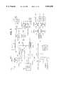
- FIG. 1is a block diagram of a memory device according to the present invention.
- FIG. 2is a more detailed block diagram of x decoder 120 depicted in FIG. 1.
- FIG. 3is a more detailed diagram of the decode logic 202 depicted in FIG. 2.
- FIG. 4is a schematic of the decode logic circuit 234 depicted in FIG. 3.
- FIG. 5is a schematic of the word line selection circuit 240 depicted in FIG. 3.
- FIG. 6is a flow chart describing how to program the memory device of FIG. 1.
- FIG. 7is a flow chart which explains how the state machine in FIG. 1 performs the programming sequence.
- FIG. 8is a flow chart which explains how to erase the memory device of FIG. 1.
- FIGS. 9A and 9Bare flow charts which explain how the state machine in FIG. 1 performs the erase sequence.
- FIG. 10is a timing diagram which explains the simultaneous read/write capability of the present invention.
- FIG. 11is a block diagram of a second embodiment memory device according to the present invention.
- FIG. 12illustrates one example of an array of memory cells suitable for use in the memory device depicted in FIG. 11.
- FIG. 1illustrates a non-volatile memory device 100 that enables simultaneous read and write operations.
- Memory device 100includes an external address input (EXT -- addr), an 8 bit data input/output (data), power inputs (not shown) and control inputs.
- the control inputsinclude chip enable (ce), output enable (oe), and write enable (we).
- the chip enable signalactivates the chip's control logic and input buffers. When chip enable is not asserted, the memory device operates in standby mode.
- Chip enable ceis received by at least the Address Transition Detector 102 and state machine and control logic 104.
- Output enableis used to gate the outputs of the device through I/O buffers during read cycles.
- Write enableis used to enable the write functions of the memory device.
- Output enable oe and write enable weare both received by state machine and control logic 104.
- all of the components of FIG. 1are contained on a single integrated circuit chip.
- Address input EXT -- addris sent to transistor 106 and Address Transition Detector 102.
- Transistor 106is connected to the input of inverter 108 and transistor 110.
- the gate of transistor 106is connected to the output of inverter 112.
- the output of inverter 108is connected to the inputs of inverters 114 and 116.
- the output of inverter 116is connected to the input of inverter 108.
- the output of inverter 114 (addr)is connected to X decode 120, Y decode 122, and Y decode 124.
- the address EXT -- addrincludes multiple bits; therefore, the circuit includes a set of components for each bit and the output of inverter(s) 114 includes multiple bits which are appropriately routed to the decoders.
- Bank 0 and Bank 1are arrays (or sets) of flash memory cells. Other non-volatile memories are also within the scope of the present invention. Although two banks are depicted in FIG. 1, the present invention will work with more than two banks. For example, many banks can be included, each bank sharing X decode 120 and having its own Y decode logic. Each bank of memory cells includes one or more sectors. Each sector includes a set of memory cells. The present invention can be used with a design that does not organize the cells into banks or sectors.
- the address decode logic for Bank 0includes X decode 120 and Y decode 122.
- X decode 120includes word line decode logic and sector decode logic for both banks.
- the address decode logic for Bank 1includes X decode 120 and Y decode 124.
- the decoders or other circuitscan include a latch to store the address being decoded.
- Address Transition Detector 102receives the external address EXT -- addr and asserts its output (labeled loadxr) when the external address EXT -- addr changes. Thus, loadxr is asserted during a read operation. Loadxr can be asserted even if other internal operations may be taking place. The signal loadxr will be processed during a write operation since a read cycle will be given the highest priority.
- the external address EXT -- addris an address generated external to the memory device; for example, a processor accessing the memory device may be generating the external address.
- the output of Address Transition Detector 102is connected to inverter 130, state machine and control logic 104 and X decode 120.
- the output of inverter 130is connected to a first input of AND gate 132.
- a second input to AND gate 132is the signal sm -- atd which is generated by state machine and control logic 104.
- the output of AND gate 132(labeled loadxw) is communicated to X decode 120, the input of inverter 112 and the gate of transistor 110. By communicated it is meant that the signal is propagated and transmitted to, either directly or indirectly via other circuit elements.
- State machine and control logic 104includes an address sequencer (or other address generator) in order to generate addresses for write operations.
- the address generated by state machine and control logic 104is labeled as SM -- addr.
- SM -- addrchanges, the signal sm -- atd is asserted by state machine and control logic 104.
- the address SM -- addris sent to transistor 110.
- EXT -- addrWhen a user accesses memory 100 an address is presented at EXT -- addr. Address transition detector 102 outputs a logic one on loadxr which forces loadxw to be logic 0, turns off transistor 110 and turns on transistor 106; therefore, selecting EXT -- addr for decoding. Thus, the signal addr carries the external address EXT -- addr to the decoders.
- FIG. 1shows multiplexer 140 with three inputs: booster0 142, VPXGG pump 144 and VCC.
- VPXGG pump 144is a positive power supply for generating and supplying a regulated positive potential to the control gate of selected flash memory cells via word lines.
- Many different voltage pumps known in the artare suitable for use in the present invention.
- a more detailed explanation of one technology which can be included in VPXGG pump 144can be found in U.S. Pat. No. 5,291,446, VPP Power Supply Having A Regulator Circuit For Controlling A Regulated Positive Potential, incorporated herein by reference.
- Booster0 142is used to boost the word line during reads.
- Multiplexer 140receives a selection signal from state machine and control logic 104 and chooses one of its three inputs to send to the word lines of Bank 0 via X decode 120.
- the output of multiplexer 140is labeled as VPXGO.
- FIG. 1is drawn to show the three inputs 142, 144 and VCC connected to a multiplexer in order to simplify the disclosure. A more detailed description of one exemplar implementation can be found in U.S. patent application Ser. No. 08/560,459, A Fast 3-State Booster Circuit, filed Nov. 17, 1995, incorporated herein by reference. Many booster circuits and selection circuits known in the art are suitable for use in the present invention.
- FIG. 1also includes multiplexer 148 having three inputs: booster1 146, VPXGG pump 144 and VCC.
- Booster1 146is similar to booster0 142.
- Multiplexer 148operates similar to multiplexer 140, and receives its selection signal from state machine and control logic 104.
- the output of multiplexer 148is VPXG1 which is sent to the word lines of Bank 1.
- the purpose of multiplexers 140 and 148is to switch the voltage depending on the operation being performed on the particular bank of memory cells.
- VPPIG pump 152is a high voltage pump used to pass high voltage to the drain of the memory cells.
- the output of VPPIG pump 152is sent to multiplexer 150 and multiplexer 154. Both multiplexers also have VCC as an input. Multiplexers 150 and 154 switch between inputs based on signals from state machine and control logic 104.
- the output of multiplexer 150is VPPI0 and the output of multiplexer 154 is VPPI1.
- VPPI1 and VPPI0are connected to VCC.
- VPPI0is connected to the gate of transistor 162.
- VPPI1is connected to the gate of transistor 164.
- the source of transistor 162is connected to Y decode 122, multiplexer 180 and multiplexer 182.
- the drain of transistor 162is connected to Dpump 170 and the drain of transistor 164.
- Dpump 170is a drain power supply.
- Various drain power supplies known in the artcan be used for the present invention.
- One exemplar drain power supplyis disclosed in U.S. Pat. No. 5,263,000, Drain Power Supply, Van Buskirk, et al., incorporated herein by reference.
- the source of transistor 164is connected to multiplexer 180, multiplexer 182 and Y decode 124.
- the connections to multiplexers 180 and 182provide a path for reading data from Bank 0 and Bank 1.
- Multiplexer 180receives a selection control signal from state machine and control logic 104 to selectively choose one of the two input signals to communicate to read sense amplifier 184.
- Multiplexer 182receives a selection control signal from state machine and control logic 104 in order to selectively communicate one of its two input signals to verify sense amplifier 186.
- Data from either Bank 0 or Bank 1can be communicated to either read sense amplifier 184 or verify sense amplifier 186. Both sense amplifiers are in communication with state machine and control logic 104. While data from Bank 0 is communicated to read sense amplifier 184, data from Bank 1 can be communicated to verify sense amplifier 186. While data from Bank 0 is communicated to verify sense amplifier 186, data from Bank 1 can be communicated to read sense amplifier 184. The output of verify sense amplifier 186 is sent to state machine and control logic 104, which is used to verify that a particular byte has been programmed or erased. Thus, data can be read from one bank while a write process is being performed on the other bank. In a different embodiment, one sense amplifier can be used for reading and verification, with its input multiplexed between the two banks.
- Data from read sense amplifier 184is sent to multiplexer 190.
- a second input of multiplexer 190includes status information from state machine and control logic 104.
- the selection signal for multiplexer 190is provided by state machine and control logic 104.
- I/O buffers 192are used to pass data out and receive data into memory device 100. While a read is being performed on one of the banks, multiplexer 190 will communicate output from read sense amplifier 184 to I/O buffers 192. During an erase or program sequence, multiplexer 190 will communicate status information to I/O buffers 192 so that an outside processor can poll memory device 100 for the status in regard to the erase or program being performed.
- Memory device 100also includes negative pump 194, which is used to generate a relatively high negative voltage to control gates of selected memory cells via word lines of either Bank 0 or Bank 1, as selected by state machine and control logic 104.
- negative pump 194is in communication with X decode 120.
- One example of a negative pumpcan be found in U.S. patent application Ser. No. 08/559,705, Low Supply Voltage Negative Charge Pump, filed Feb. 15, 1996, incorporated herein by reference.
- State machine and control logic 104provide the control for read, program and erase operations. Many of the selection lines used to select between Bank 0 and Bank 1 are controlled by state machine and control logic 104.
- Memory device 100is programmed using an embedded programming sequence and is erased using an embedded erase sequence.
- the embedded sequencesallow a processor to initiate a program or erase sequence and perform other tasks while the program and erase sequence are being carried out.
- the embedded program and erase sequencesare controlled by state machine and control logic 104, which uses a command register to manage the commencing of either sequence.
- the erase and programming operationsare only accessed via the command register, which controls an internal state machine that manages device operations. Commands are written to the command register via the data input to memory device 100.
- Bank 0includes 14 sectors (sector 0-sector 13), each sector having 64K bytes.
- Bank 1includes two sectors, sector 14 and sector 15, both of which include 64K bytes.
- Various embodimentsmay include other suitable arrangements for Bank 0 and Bank 1, including a different number of sectors, different number of bytes per sector, etc. Additionally, data can be accessed by byte, word or other suitable quantity.
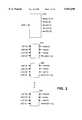
- FIG. 2shows X decode 120 in more detail.
- a first level of decode logic 202receives address addr as its input.
- X decode 120can receive thirteen address bits while the Y decodes can receive six address bit.
- First level of decode logic 202decodes the address and generates five sets of decode signals: 16 bit sel 15:0!, 8 bit xt 7:0!, 4 bit z2 3:0!, 4 bit z1 3:0! and 4 bit z0 3:0!.
- the signal sel 15:0!is used to select one of sixteen sectors. For example, if the address is accessing a byte in the first sector then sel 0! is asserted and sel 15:1! are not asserted.
- the signals xt 7:0!, z2 3:0!, z1 3:0! and z0 3:0!are used to select a particular word line in the selected sector. For exemplar purposes only, assume that each sector stores 64K bytes and there are 128 bytes per word lines; therefore; there are 512 word lines per sector.
- the output of the first level of decode logic 202is sent to sector level decode logic.
- Decode logic 204represents the sector level decode logic circuit for the first sector.
- Decode logic 206represents the sector level decode logic circuit for the second sector.
- Decode logic 208represents the sector level decode logic circuit for the sixteenth sector. Since the sixteen sector level decode logic circuits are similar and will not fit on one page of drawings, three dots are shown to represent sector level decode logic circuits for the third through fifteenth sectors.
- Each of the sector level decode logic circuitsare structurally similar; however, each has slightly different inputs and outputs.
- Each sector level decode logic circuitreceives xt 7:0!, z2 3:0!, z1 3:0!, z0 3:0!, loadxw and loadxr. Additionally, each sector level decode logic circuit receives the appropriate one of the sector select signals sel 15:0!.
- Sector level decode logic circuit for the first sector 204receives sel 0!
- sector level decode logic circuit for the second sector 206receives sel 1!
- sector level decode logic circuit for the sixteenth sector 208receives sel 15!.
- each sector level decode logic circuitSince each sector uses 512 word lines, each sector level decode logic circuit outputs 512 word lines. For example, sector level decode logic circuit 204 for the first sector outputs word lines w10 5 11:0!, sector level decode logic circuit 206 for the second sector outputs word lines w11 511:0!, . . . , sector level decode logic circuit 208 for the sixteenth sector outputs word lines w115 511:0!.
- FIG. 3illustrates sector level decode logic circuit for the first sector 204 in more detail.
- Sector select signal sel 0!is connected to transistor 220 and to a first input of AND gate 232.
- Transistor 220is also connected to the input of inverter 222 and the output of inverter 224.
- the output of inverter 222 and the input of inverter 224are connected to one input of AND gate 226.
- the signal loadxris connected to the other input of AND gate 226.
- the signal loadxwis connected to the gate of transistor 220 and to a first input of NOR gate 228.
- the output of AND gate 226is connected to a second input of NOR gate 228.
- the output of NOR gate 228is sent to inverter 230.
- inverter 230The output of inverter 230 is connected to the second input of AND gate 232.
- the output of AND gate 232is labeled as selx.
- the signal selxis, therefore, asserted when the first sector is selected and either loadxw or loadxr are asserted. Note that if state machine and control logic 104 has selected a sector for a write by previously having asserted loadxw with the appropriate sel line, e.g. sel 0!, then the input to AND gate 226 from inverter 222 is low which prevents loadxr from changing the output of AND gate 226. Thus, the same sector cannot be accessed for a read while performing a write.
- the sector level decode logic circuitincludes sixty four third level decode logic circuits. Each of the third level decode logic circuits receives selx. The third level decode logic circuits also receive one bit of z2 3:0!, one bit of z1 3:0!, and one bit of z0 3:0!. Table 1 shows which bits of z2 3:0!, z1 3:0! and z 3:01 are received by the third level decoder circuits (xin0, xin1, xin2, . . . , xin62, xin63.
- Each of the third level decode logic circuitshas an output labeled Xin#, where the first of the third level decode logic circuits (234) has an output labeled Xin0, the second of the third level decode logic circuits (236) has an output labeled Xin1, . . . , the sixty fourth of the third level decode logic circuits (238) has an output labeled Xin63.
- the signals z2, z1 and z0are used to select one of the third level decode logic circuits.
- Each of the third level decode logic circuitsare associated with eight word lines; therefore, z2, z1 and z0 are used to select a group of eight word lines.
- FIG. 3shows third level decode logic circuit 234 connected to eight word line selection circuits labeled as 240 . . . 242.
- Third level decode logic circuit 236connected to eight word line selection circuits labeled as 244 . . . 246.
- Third level decode logic circuit 238connected to eight word line selection circuits labeled as 248 ... 250.
- Each word line selection circuitis structurally the same but has different inputs and is connected to a different word line.
- the eight word line selection circuits connected to third level decode logic circuit 234 via Xin0all receive selx, but are differentiated by the signal xt 7:0!: the first word line selection circuit 240 receiving xt 0! and being connected to word line w10 0!, the second word line selection circuit receiving xt 1! and being connected to word line w10 1!, . . . , the eighth word line selection circuit 242 receiving xt 7! and being connected to word line w10 7!.
- the label for each word lineuses the following format w1# %!, where # indicates the sector and % indicates the word line number for that sector.
- the signals z2, z1 and z0select the third level decode logic circuit and, therefore, narrow down the selection to eight word lines.
- the signal xtis used to select the specific one word line from the set of eight.
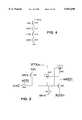
- FIG. 4is a schematic of third level decode logic circuit 234.
- the signal z0 0!is connected to the gate of transistor 270.
- the signal z1 0!is connected to the gate of transistor 272.
- the signal z2 0!is connected to the gate of transistor 274.
- the signal selxis connected to the gate of transistor 276.
- Transistor 270is connected between ground and transistor 272.
- Transistor 274is connected between transistor 276 and transistor 272.
- the drain of transistor 276is labeled as Xin0.
- FIG. 5is a schematic word line selection circuit 240.
- the signal xin0is connected to transistor 288.
- the gate of transistor 288is connected to xt 0!.
- Transistor 288is also connected to transistor 290, transistor 292, transistor 294, the gate of transistor 296 and the gate of transistor 298.
- Transistor 290is also connected to VCC and its gate is connected to selx.
- Transistor 298is connected between word line w10 0! and VPXn.
- Transistor 296is connected between XDSn and word line w10 0!.
- the gates of transistors 294 and 292are connected to word line w10 0!.
- Transistor 294is also connected to selx and transistor 292 is connected to VPXn.
- the signal VPXnis a switchable positive power supply to the word line.
- VPXnis nine volts for programming, vcc during other periods and zero volts for erase.
- the signal XDSnis a switchable negative power supply to the word line that is negative nine volts during erase.
- transistors 288, 270, 272, 274 and 276must be stronger than transistor 290 in order for the node at the gate of transistor 296 to be low. This implies that transistor 290 must be fairly weak and that is why transistor 294 has its source tied to SELX so that the node connected to the gate of transistor 296 can be pulled high without any other transistors trying to fight against it when this word line is non-selected, e.g. the path through transistors 270, 272, 274, 276 and 288 is off.
- Transistor 292, 294, 296 and 298act like an electrical latch, which is defined as an electrical device that holds its output at an appropriate voltage level, even when the input is disconnected. In this case transistors 292, 294, 296 and 298 hold the word line at the appropriate voltage (e.g. a voltage for a read operation, erase operation or program operation).
- the appropriate voltagee.g. a voltage for a read operation, erase operation or program operation.
- Address transition detector 102senses the new address and causes the external address to be forwarded to the decoders via the signal ADDR. When the address transition detector 102 determines that there is a new address, loadxr is asserted.
- X decoder 120decodes the address to select the appropriate word line.
- the selected word lineis driven and latched to the appropriate voltage level.
- New word linesare selected and deselected only during the duration of loadxr or loadxw. They are latched, meaning the address information is held (or stored) until the next occurrence of loadxr or loadxw.
- the write processwhich includes programming and erase, is performed as an embedded write process under the control of state machine and control logic 104.
- state machine and control logic 104When state machine and control logic 104 generate a new address, loadxw signal is asserted, the address is decoded and the appropriate word line is latched. Since the selected word line information is latched, the system is basically time multiplexing the X decoding path so that it can be used by the read sequence and the write sequence virtually simultaneously.
- the read sequencehas priority over the write sequence so loadxr can interrupt loadxw. If this happens, state machine and control logic 104 senses the loadxr and restarts loadxw after loadxr has finished. Loadxr is generally only active for half of the read access time in order to ensure that there will be time for loadxw to occur before the next loadxr is generated.
- the Y decodersare similar to technology known in the art. Each one determines whether the addressed cell is within the bank associated with that Y decoder. If so, the Y decoder determines the appropriate bit line.
- the x decoder of the present inventioncan be used with various y decode schemes. For example, it is within this present invention to utilize the same technology in the X decoder and the Y decoder. That is, use only one Y decoder and latch the appropriate bit line. In the embodiment of FIG. 1, which includes two banks each having its own y decoder, while one bank is being used for a write the other bank can be used for a read. If the technology of the x decoder is suitably used in the y decoder so that there is only one y decoder, then a read and write can be performed on the same bank of memory cells.
- FIG. 6illustrates the steps performed by a user of memory device 100 to program a byte in either Bank 0 or Bank 1.
- the usermust assert any necessary control signal (step 402). That is, the user must use control inputs to put the memory device 100 into program mode.
- the userit is meant a processor or other component seeking access to memory.
- the userthen inputs the embedded program set-up command (step 404) followed by the user inputting the embedded program command (step 406).
- Alternative embodimentsinclude combining steps 402, 404 and 406 into one command.
- the embedded program set-up commandstages the device for automatic programming of the addressed bytes.
- state machine and control logic 122perform the embedded program sequence. While the embedded program sequence is being performed, the user can poll memory device 100 for status (step 408). After the embedded program sequence is over, the program operation is complete (step 410).
- FIG. 7is a flow chart of the embedded program sequence controlled by state machine and control logic 104.
- the state machinereceives the set-up commands in step 502.
- the state machinereceives the program command in step 504.
- the userwrites the address of the byte to be programmed on the address input 102.
- memory device 100under the control of state machine and control logic 104, performs a preprogram verify in step 506. That is, prior to programming a byte, the device determines whether the bits in the byte are already programmed. If the necessary bits have already been programmed (step 508), then there is no need to perform the rest of the programming steps and the programming is complete (step 510).
- step 514a programming pulse is applied to the necessary bits and those bits are programmed.
- step 516the programmed byte is verified. That is, it is determined whether the programming was successful.
- step 516the device reads the byte from the respective bank and sends it to sense amplifier 186.
- step 518state machine and control logic 104 determines whether the program was successful. If the program was successful, then the program sequence is completed (step 520). If the programming was not successful, the pulse counter is incremented (step 522). The pulse counter is internal to the state machine logic. After the pulse counter is incremented, it is determined whether the pulse counter is at the maximum allowed value (step 524).
- One exemplar maximum allowed valueis 250 pulses. If the maximum value has been reached, then the program sequence has failed and the memory device 100 hangs (step 526). If the pulse counter has not reached the maximum value, then the programming step (step 514) is performed again with the additional pulse. The flow continues to steps 516 and 518 as described above.
- the state machineuses the address to determine which sector the programmed byte is within. By knowing which sector the byte is in, the state machine knows which bank the byte is in.
- state machine and control logic 104causes multiplexer 182 to select the output from the proper bank in order to send the data to verify sense amplifier 186.
- State machine and control logic 104also sends the correct control signals to multiplexers 140, 148, 150 and 154. If the byte being programmed is in Bank 0, the user is unable to read Bank 0.
- a usercan continually data poll (step 408) until the programming sequence is complete. At that point a user can then read from Bank 0. However, while the program sequence is being performed for Bank 0, a user can read from Bank 1. Similarly, while a byte is being programmed in Bank 1, a user can read from Bank 0.
- FIG. 8illustrates the steps performed by a user to erase a sector of memory device 100.
- the first step 602is to apply the proper control inputs.
- a usermust then send the embedded erase set-up command (step 604) followed by the embedded erase command (step 606).
- step 602, 604 and 606can be combined into one step.
- the embedded erase sequencecommences, under control of state machine and control logic 122. While the embedded erase sequence is proceeding, a user can poll for status (step 608).
- one of the data bitswill be designated as a status bit. This status bit will be logic 0 until the erase operation is completed. Upon completion of the erase operation, the data on that status bit will be logic 1 for a defined period of time.
- erasureis completed (step 610).
- FIGS. 9A and 9Billustrate the flow of the embedded erase sequence which is controlled by state machine and control logic 104.
- the state machinereceives that set-up command in step 712.
- the state machinereceives the erase command in step 714.
- the userthen writes the address of the sector to be erased on the address input EXT -- addr.
- memory device 100will allow a user to erase more than one sector at a time. In that case, the user will have to write more than one address.
- Steps 716 through 734are part of the process of programming all bytes prior to erase.
- state machine and control logic 104verifies whether the first byte in the addressed sector has been programmed. That is, the address of the first byte is sent, via the address sequencer internal to state machine and control logic 104, to the decoders. The addressed data is sent to verify sense amplifier 186.
- state machine and control logic 104determines whether the byte is completely programmed (e.g. the data in the byte is 00H). If the data for that byte is completely programmed then the device determines whether that byte was the last address in the sector (step 720).
- Arrow 721connects the flow chart of FIG. 9A to the flow chart of FIG. 9B.
- the flowfollows arrow 721 and moves on to the steps described in FIG. 9B. If the last address was not reached, the address sequencer is incremented (722) and steps 716 and 718 are repeated.
- step 718state machine and control logic 104 determines that the byte is not programmed, then the byte is programmed in the following steps.
- step 724the pulse counter is set.
- step 726the byte is programmed and in step 728 state machine and control logic 104 attempts to verify whether the byte has been programmed properly. If the byte has been programmed properly (step 730) then the device loops to step 720 to determine whether the byte is the last byte in the sector. If the byte was not programmed properly (step 730) then the pulse counter is incremented (step 732). If the pulse counter is at its maximum value (step 734) then memory device 100 will hang. If the pulse counter is not at its maximum value, the sequence will loop back to step 726 and there will be another attempt to program the byte. After all the bytes in the addressed sector has been programmed, the sector will be erased.
- step 740the address sequencer is initialized back to the first address of the sector and the pulse counter is reset.
- step 742the addressed sector is bulk erased using common methods known in the art for flash memories.
- step 744the device determines whether the first byte in the sector has been over-erased. If it has not, then in step 746 the device determines whether the byte being considered for overerasure is the last byte in the sector. If it was not the last byte in the sector, then the address sequencer 110 is incremented and the next byte is checked for overerase. If any byte is determined to be overerased, then, in step 770, corrections are made to compensate for the overerase.
- step 770the pulse counter is reset.
- step 772the system verifies whether the overerased cell has been properly fixed. If there is no leakage current (step 774), then the sequence loops back to step 746 and determines whether this is the last byte in the sector. Additionally, the pulse counter is set back to the value it had prior to step 770. If there is still more leakage current, then the pulse counter is incremented in step 776.
- step 778the system determines whether the pulse counter is at its maximum value. If it is, the system hangs (step 780). If the pulse counter is not at its maximum value, the system loops back to step 770 in order to perform the overerase correction again.
- the systemAfter it is determined that all the bytes had not been overerased, the system performs a byte by byte erase verify. If a particular byte is FFH then the erase for that particular byte was successful (step 750). After determining that the byte was successfully erased, the state machine determines whether the byte just considered is the last byte in the sector (step 754). If it is the last byte, then erasure is completed (step 756). If it is not the last byte, then the address sequencer is incremented (step 758) and the sequence loops back to step 750 in order to verify the next byte. If, in step 752, it is determined that the data was not FFH (e.g.
- step 760If the pulse counter was incremented to its maximum value (step 762) then the system hangs (step 764). If the pulse counter was not incremented to its maximum value, then the system loops back to step 742.
- the embedded erase sequence described abovedescribes erasing a sector. Alternatives include erasing multiple sectors or an entire bank of sectors. In each alternative, the method of FIGS. 8, 9A and 9B would be appropriately altered. For example, the pre-erase verification would need to be carried out for each sector and the bulk erase would include verifying each sector.
- FIG. 10is a timing diagram that illustrates the advantages of the present invention.
- the erase sequenceincludes preprogramming and verifying each address in the sector being erased.
- FIG. 10shows times tw0, tw1, tw2, tw3, tw4, . . . which represent write accesses to memory cells. That is, tw0 indicates a first write access to a first memory cell in the sector chosen for write, tw1 represents a second access to a second memory cell in the sector chosen for the write.
- each accessinvolves the state machine and control logic 104 generating a write address and latching an appropriate word line.
- Time tr0represents a first read operation.
- a read addressis presented at EXT -- addr.
- address transition detector 102asserts loadxr (pulse f).
- X decode 120 and the appropriate Y decodeare used to access the appropriate memory cell.
- the appropriate word lineis latched and the remainder of the read operation is performed.
- loadxwcannot be asserted.
- loadxwwas already asserted. Therefore, loadxw is interrupted. This explains why pulse b has a shorter duration than pulse a.
- loadxrSince loadxr is only asserted for half the read access time then a write access can begin, or be restarted, at tw2, which is at least (if not more than) halfway through the first read access commenced at time tr0.
- state machine and control logic 104presents a new address to the decoders and asserts loadxw (pulse c). The address from the state machine SM -- addr is decoded and the appropriate word line is latched.
- two word linesare latched during a single read access time so that two memory cells can be accessed at the same time, one for reading and one for writing.
- a usercan then request another read access at time tr1. Again a new address is presented at EXT -- addr, loadxr is asserted (pulse g), the address is decoded and the appropriate word line is latched. This process can continue allowing simultaneous read and write operations.
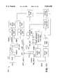
- FIG. 11illustrates a second embodiment non-volatile memory device 800 that enables simultaneous read and write operations.
- the non-volatile memory device 800includes a memory array, 822, cell array subdivided into sectors that include a dual-port structure.
- memory device 800is a flash memory and the write operations include programming operations and erase operations of flash memory cells.
- Address input EXT -- addris sent to transistor 806 and address transition detector 802.
- Transistor 806is connected to the input of inverter 808 and transistor 810.
- the gate of transistor 806is connected to the output of inverter 812.
- the output of inverter 808is connected to the input of inverters 814 and 816.
- the output of inverter 816is connected to the input of inverter 808.
- the output of inverter 814is connected to X decode 820, Y decode 824 and Y decode 828.
- Note the address EXT -- addrincludes multiple bits; therefore, the circuit includes a set of components for each bit and the output of inverter(s) 814 includes multiple bits which are appropriately routed to the decoders.
- Address transition detector 802receives the external address EXT -- addr and asserts its output when the external address EXT -- addr changes.
- the output of address transition detector 802(labeled loadxr) is connected to inverter 830, X decode 820 and state machine and control logic 844.
- the output of inverter 830is connected to AND gate 832.
- a second input to AND gate 832is a signal sm -- atd which is generated by state machine and control logic 844.
- State machine and control logic 844is similar to state machine and control logic 104.
- the output of AND gate 832(labeled loadxw) is communicated to X decode 820 and the gate of transistor 810.
- State machine and control logic 844includes an address sequencer in order to generate addresses for write operations.
- X decode 820receives the address, loadxr and loadxw in order to decode and latch the correct word line.
- X decode 820is similar to X decode 120 in FIG. 1.
- Y decode 824receives the address and uses column select 826 to select and access the appropriate bit line for write operations.
- Y decode 828receives an address and uses column select 830 to access the appropriate bit line for a read operation.
- data from cell array 822is sent, via column select 826 to verify sense amplifier 842.
- data read from cell array 822is sent, via column select 830 to read sense amplifier 834.
- the output of read sense amplifier 834is sent to multiplexer 836.
- the output of multiplexer 836is sent to driver 838 for output from device 800.
- Data from verify sense amplifier 842is sent to state machine and control logic in order to verify the appropriate data and, possibly, send status data to a user of the memory device via driver 838.
- a second input to multiplexer 836is from state machine and control logic 844. Data is sent in to state machine and control logic 844 via the data line and buffer 846.
- the device of FIG. 11is similar to the device of FIG. 1 with some exceptions. Most notably, the memory cells are not split into two banks. Rather, there is one set of memory cells divided into sectors and there are separate Y decode paths for read and write. While the write y decode path is accessing one sector the read decode path can access a different sector. Thus, a read operation can be performed in one sector while a write operation is being performed in another sector.
- FIG. 11does not show all of the voltage sources necessary for operating a non-volatile memory. These voltage sources are known in the art and adding them to FIG. 11 will only serve to clutter the drawing. In one embodiment, however, the memory device of FIG. 11 can utilize voltage sources similar to the voltage sources described with respect to FIG. 1, as are suitable.
- FIG. 12illustrates an exemplar sector of memory cells 900 for one embodiment of the device of FIG. 11.
- the architecture of the sector 900provides a dual port structure.
- Sector 900contains an array of memory cells C0-C11 which in one embodiment are implemented as flash memory cells.
- the memory cells C0-C11are each coupled to a common VSS line 902 within sector 900.
- the selection circuitry in sector 900includes a set of transistors Q0-Q11 and Q20-Q31 that selectively couple the write bit lines 910-912 and the read bit lines 920-22 to the memory cells C0-C11 as required by the particular read and program/erase operations.
- the transistors Q0-Q11 and the transistors Q20-Q31function as pass gates that are controlled by the read sector select signals 970 and the write sector select signals 980, respectively.
- the memory cells C0-C11are individually coupled to a set of interconnect lines 950-61, respectively.
- Transistors Q0-Q3selectively couple the read bit line 920 to the memory cells C0-C3 under control of the read sector select signals 970.
- the transistors Q4-Q7selectively couple the read bit line 921 to the memory cells C4-C7 under control of the read sector select signals 970.
- the transistors Q8-Q11selectively couple the read bit line 922 to the memory cells C8-C11 under control of the read sector select signals 970.
- activating read sector select signal 971couples memory cells C0, C4, and C8 to the read bit lines 920, 921, and 922, respectively, during read operations.
- activating read sector select signal 972couples memory cells C1, C5, and C9 to the read bit lines 920, 921, and 922, respectively, during a read operation.
- Transistors Q20-Q23selectively couple the write bit line 910 to the memory cells C0-C3 under control of the write sector select signals 980.
- Transistors Q24-Q27selectively couple the write bit line 911 to the memory cells C4-C7 under control of the write sector select signals 980.
- the transistors Q28-Q31selectively couple the write bit line 912 to the flash memory cells C8-C11 under control of the write sector select signals 980.
- activating write sector select signal 981couples memory cells C3, C7, and C11 to the write bit lines 910, 911, and 912, respectively, during a program or erase operation.
- activating write sector select signal 982couples memory cells C2, C6, and C10 to the write bit lines 910, 911 and 912 respectively, during a program or erase operation.
- only a subset of the array sectorscontain the selection circuitry that enables simultaneous read and program/erase operations.
- Such a restriction of simultaneous read and program/eraselowers the cost and die space consumed by the read bit line and write bit line selection circuitry for systems that require only small areas of random access to the non-volatile memory device.
- FIGS. 1 and 11have only one word (or word line) decode path. That is, there is only one address line for x decode, one x decoder and one set of word lines. Having only one x decode path saves space on the memory device.
- the technology discussed above with respect to the x decode pathcan be used with many different memory architectures and y decode designs.
- FIGS. 1 and 11only show two of the many different designs that can utilize the technology of the present invention.
- Alternative embodimentscan also utilize the technology described herein for the y decode path so that the bit lines are latched.
- one alternativeincludes using latches for the bit lines and the word lines while a second alternative includes using latches for the bit lines and not using latches for the word lines.
Landscapes
- Engineering & Computer Science (AREA)
- Microelectronics & Electronic Packaging (AREA)
- Read Only Memory (AREA)
- Static Random-Access Memory (AREA)
Abstract
Description
TABLE 1 ______________________________________ Circuit z2 3:0! z1 3:0! zo 3:0! ______________________________________ Xin0 (234) z2 0! z1 0! z0 0! Xin1 (236) z2 0! z1 0! z0 1!Xin2 z2 0! z1 0! z0 2!Xin3 z2 0! z1 0! z0 3!Xin4 z2 0! z1 1! z0 0!Xin5 z2 0! z1 1! z0 1!Xin6 z2 0! z1 1! z0 2!Xin7 z2 0! z1 1! z0 3!Xin8 z2 0! z1 2! z0 0!Xin9 z2 0! z1 2! z0 1!Xin10 z2 0! z1 2! z0 2!Xin11 z2 0! z1 2! z0 3!Xin12 z2 0! z1 3! z0 0!Xin13 z2 0! z1 3! z0 1!Xin14 z2 0! z1 3! z0 2!Xin15 z2 0! z1 3! z0 3!Xin16 z2 1! z1 0! z0 0!Xin17 z2 1! z1 0! z0 1!Xin18 z2 1! z1 0! z0 2!Xin19 z2 1! z1 0! z0 3!Xin20 z2 1! z1 1! z0 0!Xin21 z2 1! z1 1! z0 1!Xin22 z2 1! z1 1! z0 2!Xin23 z2 1! z1 1! z0 3!Xin24 z2 1! z1 2! z0 0!Xin25 z2 1! z1 2! z0 1!Xin26 z2 1! z1 2! z0 2!Xin27 z2 1! z1 2! z0 3!Xin28 z2 1! z1 3! z0 0!Xin29 z2 1! z1 3! z0 1!Xin30 z2 1! z1 3! z0 2!Xin31 z2 1! z1 3! z0 3! Xin32 z2 2! z1 0! z0 0! Xin33 z2 2! z1 0! z0 1! Xin34 z2 2! z1 0! z0 2! Xin35 z2 2! z1 0! z0 3! Xin36 z2 2! z1 1! z0 0! Xin37 z2 2! z1 1! z0 1! Xin38 z2 2! z1 1! z0 2! Xin39 z2 2! z1 1! z0 3! Xin40 z2 2! z1 2! z0 0! Xin41 z2 2! z1 2! z0 1! Xin42 z2 2! z1 2! z0 2! Xin43 z2 2! z1 2! z0 3! Xin44 z2 2! z1 3! z0 0! Xin45 z2 2! z1 3! z0 1! Xin46 z2 2! z1 3! z6 2! Xin47 z2 2! z1 3! z0 3!Xin48 z2 3! z1 0! z0 0!Xin49 z2 3! z1 0! z0 1!Xin50 z2 3! z1 0! z0 2!Xin51 z2 3! z1 0! z0 3!Xin52 z2 3! z1 1! z0 0!Xin53 z2 3! z1 1! z0 1!Xin54 z2 3! z1 1! z0 2!Xin55 z2 3! z1 1! z0 3!Xin56 z2 3! z1 2! z0 0!Xin57 z2 3! z1 2! z0 1!Xin58 z2 3! z1 2! z0 2!Xin59 z2 3! z1 2! z0 3!Xin60 z2 3! z1 3! z0 0!Xin61 z2 3! z1 3! z0 1!Xin62 z2 3! z1 3! z0 2! Xin63 (238) z2 3! z1 3! z0 3! ______________________________________
Claims (40)
Priority Applications (7)
| Application Number | Priority Date | Filing Date | Title |
|---|---|---|---|
| US08/811,683US5841696A (en) | 1997-03-05 | 1997-03-05 | Non-volatile memory enabling simultaneous reading and writing by time multiplexing a decode path |
| DE69707715TDE69707715T2 (en) | 1997-03-05 | 1997-08-15 | NON-VOLATILE MEMORY ALLOWING READING AND WRITING ALLOWED BY TIME MULTIPLEXING A DATA PATH |
| KR10-1999-7008101AKR100537816B1 (en) | 1997-03-05 | 1997-08-15 | Non-volatile memory enabling simultaneous reading and writing by time multiplexing a decode path |
| EP97937295AEP0965130B1 (en) | 1997-03-05 | 1997-08-15 | Non-volatile memory enabling simultaneous reading and writing by time multiplexing a decode path |
| JP53849198AJP3931249B2 (en) | 1997-03-05 | 1997-08-15 | Nonvolatile memory that enables simultaneous reading and writing by time-multiplexing the decoding path |
| PCT/US1997/014454WO1998039773A1 (en) | 1997-03-05 | 1997-08-15 | Non-volatile memory enabling simultaneous reading and writing by time multiplexing a decode path |
| TW086118217ATW359835B (en) | 1997-03-05 | 1997-12-04 | Non-volatile memory enabling simultaneous reading and writing by time multiplexing a decode path |
Applications Claiming Priority (1)
| Application Number | Priority Date | Filing Date | Title |
|---|---|---|---|
| US08/811,683US5841696A (en) | 1997-03-05 | 1997-03-05 | Non-volatile memory enabling simultaneous reading and writing by time multiplexing a decode path |
Publications (1)
| Publication Number | Publication Date |
|---|---|
| US5841696Atrue US5841696A (en) | 1998-11-24 |
Family
ID=25207250
Family Applications (1)
| Application Number | Title | Priority Date | Filing Date |
|---|---|---|---|
| US08/811,683Expired - LifetimeUS5841696A (en) | 1997-03-05 | 1997-03-05 | Non-volatile memory enabling simultaneous reading and writing by time multiplexing a decode path |
Country Status (7)
| Country | Link |
|---|---|
| US (1) | US5841696A (en) |
| EP (1) | EP0965130B1 (en) |
| JP (1) | JP3931249B2 (en) |
| KR (1) | KR100537816B1 (en) |
| DE (1) | DE69707715T2 (en) |
| TW (1) | TW359835B (en) |
| WO (1) | WO1998039773A1 (en) |
Cited By (35)
| Publication number | Priority date | Publication date | Assignee | Title |
|---|---|---|---|---|
| US6005803A (en)* | 1998-09-23 | 1999-12-21 | Advanced Micro Devices, Inc. | Memory address decoding circuit for a simultaneous operation flash memory device with a flexible bank partition architecture |
| US6033955A (en)* | 1998-09-23 | 2000-03-07 | Advanced Micro Devices, Inc. | Method of making flexibly partitioned metal line segments for a simultaneous operation flash memory device with a flexible bank partition architecture |
| US6094095A (en)* | 1998-06-29 | 2000-07-25 | Cypress Semiconductor Corp. | Efficient pump for generating voltages above and/or below operating voltages |
| US6111787A (en)* | 1999-10-19 | 2000-08-29 | Advanced Micro Devices, Inc. | Address transistion detect timing architecture for a simultaneous operation flash memory device |
| US6118698A (en)* | 1999-10-19 | 2000-09-12 | Advanced Micro Devices, Inc. | Output multiplexing implementation for a simultaneous operation flash memory device |
| US6125055A (en)* | 1999-10-19 | 2000-09-26 | Advanced Micro Devices, Inc. | Sector write protect CAMS for a simultaneous operation flash memory |
| US6163478A (en)* | 1999-10-19 | 2000-12-19 | Advanced Micro Devices, Inc. | Common flash interface implementation for a simultaneous operation flash memory device |
| US6166982A (en)* | 1998-06-25 | 2000-12-26 | Cypress Semiconductor Corp. | High voltage switch for eeprom/flash memories |
| US6172553B1 (en) | 1998-06-25 | 2001-01-09 | Cypress Semiconductor Corp. | High voltage steering network for EEPROM/FLASH memory |
| US6178132B1 (en)* | 1999-09-09 | 2001-01-23 | Macronix International Co., Ltd. | Non-volatile integrated circuit having read while write capability using one address register |
| US6208561B1 (en)* | 2000-06-13 | 2001-03-27 | Advanced Micro Devices, Inc. | Method to reduce capacitive loading in flash memory X-decoder for accurate voltage control at wordlines and select lines |
| US6275894B1 (en) | 1998-09-23 | 2001-08-14 | Advanced Micro Devices, Inc. | Bank selector circuit for a simultaneous operation flash memory device with a flexible bank partition architecture |
| US6285585B1 (en) | 1999-10-19 | 2001-09-04 | Advaned Micro Devices, Inc. | Output switching implementation for a flash memory device |
| US6327181B1 (en) | 1999-10-19 | 2001-12-04 | Advanced Micro Devices Inc. | Reference cell bitline path architecture for a simultaneous operation flash memory device |
| US6331950B1 (en) | 1999-10-19 | 2001-12-18 | Fujitsu Limited | Write protect input implementation for a simultaneous operation flash memory device |
| US6335883B1 (en) | 1997-05-23 | 2002-01-01 | Ricoh Company, Ltd. | Memory configuration of a composite memory device |
| US6359808B1 (en)* | 1999-10-19 | 2002-03-19 | Advanced Micro Devices, Inc. | Low voltage read cascode for 2V/3V and different bank combinations without metal options for a simultaneous operation flash memory device |
| US6550028B1 (en) | 1999-10-19 | 2003-04-15 | Advanced Micro Devices, Inc. | Array VT mode implementation for a simultaneous operation flash memory device |
| US6552935B2 (en) | 2001-08-02 | 2003-04-22 | Stmicroelectronics, Inc. | Dual bank flash memory device and method |
| US6571307B1 (en) | 1999-10-19 | 2003-05-27 | Advanced Micro Devices, Inc. | Multiple purpose bus for a simultaneous operation flash memory device |
| US6584034B1 (en) | 2001-04-23 | 2003-06-24 | Aplus Flash Technology Inc. | Flash memory array structure suitable for multiple simultaneous operations |
| US6654848B1 (en)* | 2000-09-15 | 2003-11-25 | Advanced Micro Devices, Inc. | Simultaneous execution command modes in a flash memory device |
| US6717852B2 (en) | 2001-10-11 | 2004-04-06 | Kabushiki Kaisha Toshiba | Nonvolatile semiconductor memory device capable of concurrently and reliably writing/erasing and reading memory cores |
| US6781914B2 (en) | 2001-08-23 | 2004-08-24 | Winbond Electronics Corp. | Flash memory having a flexible bank partition |
| US20040190343A1 (en)* | 2003-03-25 | 2004-09-30 | Jongmin Park | Nonvolatile memories with asymmetric transistors, nonvolatile memories with high voltage lines extending in the column direction, and nonvolatile memories with decoding circuits sharing a common area |
| US20050073894A1 (en)* | 2000-06-30 | 2005-04-07 | Micron Technology, Inc. | Zero latency-zero bus turnaround synchronous flash memory |
| US6883037B2 (en)* | 2001-03-21 | 2005-04-19 | Microsoft Corporation | Fast data decoder that operates with reduced output buffer bounds checking |
| US20050141273A1 (en)* | 2003-12-31 | 2005-06-30 | Min-Gun Park | Flash memory system capable of inputting/outputting sector data at random |
| US20050276108A1 (en)* | 2004-06-15 | 2005-12-15 | Guterman Daniel C | Concurrent programming of non-volatile memory |
| US7099226B2 (en) | 2003-10-14 | 2006-08-29 | Atmel Corporation | Functional register decoding system for multiple plane operation |
| US20070204101A1 (en)* | 2006-02-22 | 2007-08-30 | Masaharu Adachi | Nonvolatile memory card |
| US20100085822A1 (en)* | 2008-10-06 | 2010-04-08 | Tianhong Yan | Continuous programming of non-volatile memory |
| US7859240B1 (en) | 2007-05-22 | 2010-12-28 | Cypress Semiconductor Corporation | Circuit and method for preventing reverse current flow into a voltage regulator from an output thereof |
| US8711596B2 (en) | 2009-04-20 | 2014-04-29 | Sandisk 3D Llc | Memory system with data line switching scheme |
| US8913413B2 (en) | 2008-08-25 | 2014-12-16 | Sandisk 3D Llc | Memory system with sectional data lines |
Families Citing this family (3)
| Publication number | Priority date | Publication date | Assignee | Title |
|---|---|---|---|---|
| JP4524439B2 (en)* | 2000-03-30 | 2010-08-18 | ラウンド ロック リサーチ、エルエルシー | Synchronous flash memory with zero latency and zero bus turnaround functions |
| KR100600301B1 (en)* | 2005-05-25 | 2006-07-13 | 주식회사 하이닉스반도체 | Page buffer circuit with reduced area, flash memory device comprising same, and program operation method thereof |
| JP5453078B2 (en)* | 2009-12-24 | 2014-03-26 | 三星電子株式会社 | Nonvolatile memory control device and control method |
Citations (13)
| Publication number | Priority date | Publication date | Assignee | Title |
|---|---|---|---|---|
| EP0212451A2 (en)* | 1985-08-16 | 1987-03-04 | Fujitsu Limited | A semiconductor memory device having two column transfer gate transistor groups independently provided for a sense amplifier and a programming circuit |
| US4752871A (en)* | 1985-09-30 | 1988-06-21 | Motorola, Inc. | Single-chip microcomputer having a program register for controlling two EEPROM arrays |
| EP0372873A2 (en)* | 1988-12-05 | 1990-06-13 | Texas Instruments Incorporated | Integrated-circuit configuration having fast local access time |
| EP0376285A2 (en)* | 1988-12-27 | 1990-07-04 | Nec Corporation | Microcomputer having electrically erasable and programmable nonvolatile memory |
| US5007022A (en)* | 1987-12-21 | 1991-04-09 | Texas Instruments Incorporated | Two-port two-transistor DRAM |
| US5241510A (en)* | 1991-01-11 | 1993-08-31 | Kabushiki Kaisha Toshiba | Semiconductor integrated circuit |
| US5245572A (en)* | 1991-07-30 | 1993-09-14 | Intel Corporation | Floating gate nonvolatile memory with reading while writing capability |
| US5276642A (en)* | 1991-07-15 | 1994-01-04 | Micron Technology, Inc. | Method for performing a split read/write operation in a dynamic random access memory |
| US5355334A (en)* | 1993-01-13 | 1994-10-11 | Nec Corporation | Nonvolatile semiconductor memory device having parallel write and read function |
| US5506810A (en)* | 1994-08-16 | 1996-04-09 | Cirrus Logic, Inc. | Dual bank memory and systems using the same |
| EP0745995A1 (en)* | 1995-05-05 | 1996-12-04 | STMicroelectronics S.r.l. | Nonvolatile, in particular flash-EEPROM, memory device |
| US5684752A (en)* | 1994-06-03 | 1997-11-04 | Intel Corporation | Pipelined read architecture for memory |
| US5691955A (en)* | 1995-09-05 | 1997-11-25 | Mitsubishi Denki Kabushiki Kaisha | Synchronous semiconductor memory device operating in synchronization with external clock signal |
Family Cites Families (4)
| Publication number | Priority date | Publication date | Assignee | Title |
|---|---|---|---|---|
| JPS6386197A (en)* | 1986-09-29 | 1988-04-16 | Mitsubishi Electric Corp | Nonvolatile semiconductor memory device |
| JPS63161599A (en)* | 1986-12-25 | 1988-07-05 | Toshiba Corp | non-volatile semiconductor memory |
| JP3143161B2 (en)* | 1991-08-29 | 2001-03-07 | 三菱電機株式会社 | Non-volatile semiconductor memory |
| JP3464271B2 (en)* | 1994-04-12 | 2003-11-05 | 三菱電機株式会社 | Nonvolatile semiconductor memory device |
- 1997
- 1997-03-05USUS08/811,683patent/US5841696A/ennot_activeExpired - Lifetime
- 1997-08-15DEDE69707715Tpatent/DE69707715T2/ennot_activeExpired - Lifetime
- 1997-08-15EPEP97937295Apatent/EP0965130B1/ennot_activeExpired - Lifetime
- 1997-08-15JPJP53849198Apatent/JP3931249B2/ennot_activeExpired - Fee Related
- 1997-08-15WOPCT/US1997/014454patent/WO1998039773A1/enactiveIP Right Grant
- 1997-08-15KRKR10-1999-7008101Apatent/KR100537816B1/ennot_activeExpired - Fee Related
- 1997-12-04TWTW086118217Apatent/TW359835B/enactive
Patent Citations (14)
| Publication number | Priority date | Publication date | Assignee | Title |
|---|---|---|---|---|
| EP0212451A2 (en)* | 1985-08-16 | 1987-03-04 | Fujitsu Limited | A semiconductor memory device having two column transfer gate transistor groups independently provided for a sense amplifier and a programming circuit |
| US4752871A (en)* | 1985-09-30 | 1988-06-21 | Motorola, Inc. | Single-chip microcomputer having a program register for controlling two EEPROM arrays |
| US5007022A (en)* | 1987-12-21 | 1991-04-09 | Texas Instruments Incorporated | Two-port two-transistor DRAM |
| EP0372873A2 (en)* | 1988-12-05 | 1990-06-13 | Texas Instruments Incorporated | Integrated-circuit configuration having fast local access time |
| EP0376285A2 (en)* | 1988-12-27 | 1990-07-04 | Nec Corporation | Microcomputer having electrically erasable and programmable nonvolatile memory |
| US5241510A (en)* | 1991-01-11 | 1993-08-31 | Kabushiki Kaisha Toshiba | Semiconductor integrated circuit |
| US5276642A (en)* | 1991-07-15 | 1994-01-04 | Micron Technology, Inc. | Method for performing a split read/write operation in a dynamic random access memory |
| US5245572A (en)* | 1991-07-30 | 1993-09-14 | Intel Corporation | Floating gate nonvolatile memory with reading while writing capability |
| US5361343A (en)* | 1991-07-30 | 1994-11-01 | Intel Corporation | Microprocessor system including first and second nonvolatile memory arrays which may be simultaneously read and reprogrammed |
| US5355334A (en)* | 1993-01-13 | 1994-10-11 | Nec Corporation | Nonvolatile semiconductor memory device having parallel write and read function |
| US5684752A (en)* | 1994-06-03 | 1997-11-04 | Intel Corporation | Pipelined read architecture for memory |
| US5506810A (en)* | 1994-08-16 | 1996-04-09 | Cirrus Logic, Inc. | Dual bank memory and systems using the same |
| EP0745995A1 (en)* | 1995-05-05 | 1996-12-04 | STMicroelectronics S.r.l. | Nonvolatile, in particular flash-EEPROM, memory device |
| US5691955A (en)* | 1995-09-05 | 1997-11-25 | Mitsubishi Denki Kabushiki Kaisha | Synchronous semiconductor memory device operating in synchronization with external clock signal |
Non-Patent Citations (6)
| Title |
|---|
| Atmel, 4 Megabit 2.7 volt Battery Voltage 0 Flash with 256 K EEPROM CMOS Combination Memory AT29BV432 AWAKE Memory Architecture.* |
| Atmel, 4 Megabit 2.7-volt Battery-Voltage™0 Flash with 256 K EEPROM CMOS Combination Memory--AT29BV432 AWAKE™ Memory Architecture. |
| Atmel, 4 Megabit 5 volt Flash with 256K E 2 PROM Memory AT29C432 ConcurrentFlash .* |
| Atmel, 4 Megabit 5-volt Flash with 256K E2 PROM Memory--AT29C432 ConcurrentFlash™. |
| J., Kruckeberg, "Zweigeteiltes EEPROM: Gleichzeitig auslesen und beschreiben," Elektronik, No. 26, 1990, pp. 56-59. |
| J., Kruckeberg, Zweigeteiltes EEPROM: Gleichzeitig auslesen und beschreiben, Elektronik, No. 26, 1990, pp. 56 59.* |
Cited By (69)
| Publication number | Priority date | Publication date | Assignee | Title |
|---|---|---|---|---|
| US20090091984A1 (en)* | 1997-05-23 | 2009-04-09 | Ricoh Company, Ltd. | Memory configuration of a composite memory device |
| US6335883B1 (en) | 1997-05-23 | 2002-01-01 | Ricoh Company, Ltd. | Memory configuration of a composite memory device |
| US6545916B2 (en) | 1997-05-23 | 2003-04-08 | Ricoh Company, Ltd. | Memory configuration of a composite memory device |
| US7969791B2 (en) | 1997-05-23 | 2011-06-28 | Ricoh Company, Ltd. | Memory configuration of a composite memory device |
| US20100103739A1 (en)* | 1997-05-23 | 2010-04-29 | Ricoh Company, Ltd. | Memory configuration of a composite memory device |
| US7672172B2 (en) | 1997-05-23 | 2010-03-02 | Ricoh Company, Ltd. | Memory configuration of a composite memory device |
| USRE40917E1 (en)* | 1997-05-23 | 2009-09-15 | Ricoh Company, Ltd. | Memory configuration of a composite memory device |
| US20030210588A1 (en)* | 1997-05-23 | 2003-11-13 | Minoru Fukuda | Memory configuration of a composite memory device |
| US7483312B2 (en) | 1997-05-23 | 2009-01-27 | Ricoh Company, Ltd | Memory configuration of a composite memory device |
| US6172553B1 (en) | 1998-06-25 | 2001-01-09 | Cypress Semiconductor Corp. | High voltage steering network for EEPROM/FLASH memory |
| US6166982A (en)* | 1998-06-25 | 2000-12-26 | Cypress Semiconductor Corp. | High voltage switch for eeprom/flash memories |
| US6094095A (en)* | 1998-06-29 | 2000-07-25 | Cypress Semiconductor Corp. | Efficient pump for generating voltages above and/or below operating voltages |
| US6470414B2 (en) | 1998-09-23 | 2002-10-22 | Advanced Micro Devices, Inc. | Bank selector circuit for a simultaneous operation flash memory device with a flexible bank partition architecture |
| US6275894B1 (en) | 1998-09-23 | 2001-08-14 | Advanced Micro Devices, Inc. | Bank selector circuit for a simultaneous operation flash memory device with a flexible bank partition architecture |
| US6633949B2 (en) | 1998-09-23 | 2003-10-14 | Advanced Micro Devices, Inc. | Bank selector circuit for a simultaneous operation flash memory device with a flexible bank partition architecture |
| US6005803A (en)* | 1998-09-23 | 1999-12-21 | Advanced Micro Devices, Inc. | Memory address decoding circuit for a simultaneous operation flash memory device with a flexible bank partition architecture |
| US6033955A (en)* | 1998-09-23 | 2000-03-07 | Advanced Micro Devices, Inc. | Method of making flexibly partitioned metal line segments for a simultaneous operation flash memory device with a flexible bank partition architecture |
| US6178132B1 (en)* | 1999-09-09 | 2001-01-23 | Macronix International Co., Ltd. | Non-volatile integrated circuit having read while write capability using one address register |
| US6331950B1 (en) | 1999-10-19 | 2001-12-18 | Fujitsu Limited | Write protect input implementation for a simultaneous operation flash memory device |
| US6208556B1 (en)* | 1999-10-19 | 2001-03-27 | Advanced Micro Devices, Inc. | Address transition detect timing architecture for a simultaneous operation flash memory device |
| US6327181B1 (en) | 1999-10-19 | 2001-12-04 | Advanced Micro Devices Inc. | Reference cell bitline path architecture for a simultaneous operation flash memory device |
| US6550028B1 (en) | 1999-10-19 | 2003-04-15 | Advanced Micro Devices, Inc. | Array VT mode implementation for a simultaneous operation flash memory device |
| US6111787A (en)* | 1999-10-19 | 2000-08-29 | Advanced Micro Devices, Inc. | Address transistion detect timing architecture for a simultaneous operation flash memory device |
| US6571307B1 (en) | 1999-10-19 | 2003-05-27 | Advanced Micro Devices, Inc. | Multiple purpose bus for a simultaneous operation flash memory device |
| US6118698A (en)* | 1999-10-19 | 2000-09-12 | Advanced Micro Devices, Inc. | Output multiplexing implementation for a simultaneous operation flash memory device |
| US6285585B1 (en) | 1999-10-19 | 2001-09-04 | Advaned Micro Devices, Inc. | Output switching implementation for a flash memory device |
| US6125055A (en)* | 1999-10-19 | 2000-09-26 | Advanced Micro Devices, Inc. | Sector write protect CAMS for a simultaneous operation flash memory |
| US6275412B1 (en) | 1999-10-19 | 2001-08-14 | Advanced Micro Devices, Inc. | Common flash interface implementation for a simultaneous operation flash memory device |
| US6359808B1 (en)* | 1999-10-19 | 2002-03-19 | Advanced Micro Devices, Inc. | Low voltage read cascode for 2V/3V and different bank combinations without metal options for a simultaneous operation flash memory device |
| US6163478A (en)* | 1999-10-19 | 2000-12-19 | Advanced Micro Devices, Inc. | Common flash interface implementation for a simultaneous operation flash memory device |
| US6208561B1 (en)* | 2000-06-13 | 2001-03-27 | Advanced Micro Devices, Inc. | Method to reduce capacitive loading in flash memory X-decoder for accurate voltage control at wordlines and select lines |
| US20050073894A1 (en)* | 2000-06-30 | 2005-04-07 | Micron Technology, Inc. | Zero latency-zero bus turnaround synchronous flash memory |
| US6654848B1 (en)* | 2000-09-15 | 2003-11-25 | Advanced Micro Devices, Inc. | Simultaneous execution command modes in a flash memory device |
| US6957297B1 (en)* | 2000-09-15 | 2005-10-18 | Advanced Micro Devices, Inc. | Simultaneous execution command modes in a flash memory device |
| US7634592B2 (en) | 2001-03-21 | 2009-12-15 | Microsoft Corporation | Method, system, and program for hibernation of computer systems having DMA controller to asynchronously read data from buffers |
| US6963934B2 (en) | 2001-03-21 | 2005-11-08 | Microsoft Corporation | Hibernation of computer systems |
| US6883037B2 (en)* | 2001-03-21 | 2005-04-19 | Microsoft Corporation | Fast data decoder that operates with reduced output buffer bounds checking |
| US20050097239A1 (en)* | 2001-03-21 | 2005-05-05 | Microsoft Corporation | Hibernation of computer systems |
| US20050108589A1 (en)* | 2001-03-21 | 2005-05-19 | Microsoft Corporation | Hibernation of computer systems |
| US7305502B2 (en) | 2001-03-21 | 2007-12-04 | Microsoft Corporation | Compressing an amount of uncompressed data less than amount of hibernation related data written to storage via DMA controller when requested write is pending |
| US20050149646A1 (en)* | 2001-03-21 | 2005-07-07 | Microsoft Corporation | Hibernation of computer systems |
| US6788612B2 (en) | 2001-04-23 | 2004-09-07 | Aplus Flash Technology, Inc. | Flash memory array structure suitable for multiple simultaneous operations |
| US6788611B2 (en) | 2001-04-23 | 2004-09-07 | Aplus Flash Technology, Inc. | Flash memory array structure suitable for multiple simultaneous operations |
| US6584034B1 (en) | 2001-04-23 | 2003-06-24 | Aplus Flash Technology Inc. | Flash memory array structure suitable for multiple simultaneous operations |
| US20030206455A1 (en)* | 2001-04-23 | 2003-11-06 | Aplus Flash Technology, Inc. | Novel flash memory array structure suitable for multiple simultaneous operations |
| US6552935B2 (en) | 2001-08-02 | 2003-04-22 | Stmicroelectronics, Inc. | Dual bank flash memory device and method |
| US6781914B2 (en) | 2001-08-23 | 2004-08-24 | Winbond Electronics Corp. | Flash memory having a flexible bank partition |
| US6717852B2 (en) | 2001-10-11 | 2004-04-06 | Kabushiki Kaisha Toshiba | Nonvolatile semiconductor memory device capable of concurrently and reliably writing/erasing and reading memory cores |
| US7046551B2 (en)* | 2003-03-25 | 2006-05-16 | Mosel Vitelic, Inc. | Nonvolatile memories with asymmetric transistors, nonvolatile memories with high voltage lines extending in the column direction, and nonvolatile memories with decoding circuits sharing a common area |
| US20040190343A1 (en)* | 2003-03-25 | 2004-09-30 | Jongmin Park | Nonvolatile memories with asymmetric transistors, nonvolatile memories with high voltage lines extending in the column direction, and nonvolatile memories with decoding circuits sharing a common area |
| US7099226B2 (en) | 2003-10-14 | 2006-08-29 | Atmel Corporation | Functional register decoding system for multiple plane operation |
| US20050141273A1 (en)* | 2003-12-31 | 2005-06-30 | Min-Gun Park | Flash memory system capable of inputting/outputting sector data at random |
| US20080055994A1 (en)* | 2004-06-15 | 2008-03-06 | Guterman Daniel C | Concurrent programming of non-volatile memory |
| US20080056002A1 (en)* | 2004-06-15 | 2008-03-06 | Guterman Daniel C | Concurrent programming of non-volatile memory |
| US20080056003A1 (en)* | 2004-06-15 | 2008-03-06 | Guterman Daniel C | Concurrent programming of non-volatile memory |
| US20050276108A1 (en)* | 2004-06-15 | 2005-12-15 | Guterman Daniel C | Concurrent programming of non-volatile memory |
| US7570518B2 (en) | 2004-06-15 | 2009-08-04 | Sandisk Corporation | Concurrent programming of non-volatile memory |
| US7307884B2 (en) | 2004-06-15 | 2007-12-11 | Sandisk Corporation | Concurrent programming of non-volatile memory |
| US7796444B2 (en) | 2004-06-15 | 2010-09-14 | Sandisk Corporation | Concurrent programming of non-volatile memory |
| US7821835B2 (en) | 2004-06-15 | 2010-10-26 | Sandisk Corporation | Concurrent programming of non-volatile memory |
| US7904638B2 (en)* | 2006-02-22 | 2011-03-08 | Ricoh Company, Ltd. | Nonvolatile memory card having improved compatibility with different memory card standards |
| US20070204101A1 (en)* | 2006-02-22 | 2007-08-30 | Masaharu Adachi | Nonvolatile memory card |
| US7859240B1 (en) | 2007-05-22 | 2010-12-28 | Cypress Semiconductor Corporation | Circuit and method for preventing reverse current flow into a voltage regulator from an output thereof |
| US8913413B2 (en) | 2008-08-25 | 2014-12-16 | Sandisk 3D Llc | Memory system with sectional data lines |
| US20100085822A1 (en)* | 2008-10-06 | 2010-04-08 | Tianhong Yan | Continuous programming of non-volatile memory |
| US8238174B2 (en) | 2008-10-06 | 2012-08-07 | Sandisk 3D Llc | Continuous programming of non-volatile memory |
| US8780651B2 (en) | 2008-10-06 | 2014-07-15 | Sandisk 3D Llc | Continuous programming of non-volatile memory |
| US8027209B2 (en) | 2008-10-06 | 2011-09-27 | Sandisk 3D, Llc | Continuous programming of non-volatile memory |
| US8711596B2 (en) | 2009-04-20 | 2014-04-29 | Sandisk 3D Llc | Memory system with data line switching scheme |
Also Published As
| Publication number | Publication date |
|---|---|
| DE69707715T2 (en) | 2002-07-11 |
| EP0965130A1 (en) | 1999-12-22 |
| EP0965130B1 (en) | 2001-10-24 |
| KR20000076015A (en) | 2000-12-26 |
| TW359835B (en) | 1999-06-01 |
| DE69707715D1 (en) | 2001-11-29 |
| JP2001512613A (en) | 2001-08-21 |
| WO1998039773A1 (en) | 1998-09-11 |
| KR100537816B1 (en) | 2005-12-20 |
| JP3931249B2 (en) | 2007-06-13 |
Similar Documents
| Publication | Publication Date | Title |
|---|---|---|
| US5841696A (en) | Non-volatile memory enabling simultaneous reading and writing by time multiplexing a decode path | |
| US5867430A (en) | Bank architecture for a non-volatile memory enabling simultaneous reading and writing | |
| US6735116B2 (en) | NAND-type flash memory device with multi-page program, multi-page read, multi-block erase operations | |
| JP3863005B2 (en) | Memory cell decoder and semiconductor memory device having the same | |
| US6304510B1 (en) | Memory device address decoding | |
| US7957201B2 (en) | Flash memory device operating at multiple speeds | |
| JPH11224492A (en) | Semiconductor storage device, nonvolatile semiconductor storage device, and flash memory | |
| WO2006011213A1 (en) | Method for initializing non-volatile storage device, and non-volatile storage device | |
| US20010053091A1 (en) | Nonvolatile memory with background operation function | |
| US6457093B2 (en) | Circuit and method to control operations of another circuit | |
| US7102927B2 (en) | Memory devices and programming methods that simultaneously store erase status indications for memory blocks | |
| US20030107923A1 (en) | Flash memory having separate read and write paths | |
| JP2766082B2 (en) | Semiconductor storage device | |
| US6515900B2 (en) | Non-volatile memory with background operation function | |
| JP2001028191A (en) | Automatic erasing method for nonvolatile semiconductor memory | |
| US6622201B1 (en) | Chained array of sequential access memories enabling continuous read | |
| JP2002163892A (en) | Nonvolatile semiconductor memory and operation method | |
| JP3187121B2 (en) | Semiconductor storage device | |
| EP0933778B1 (en) | Nonvolatile semiconductor memory | |
| JPH0482095A (en) | Non-volatile semiconductor memory device | |
| JP3541427B2 (en) | Flash memory | |
| JP2002093179A (en) | Non-volatile semiconductor memory | |
| JP2002093183A (en) | Non-volatile semiconductor memory | |
| JP2002008383A (en) | Nonvolatile semiconductor memory and operation method | |
| JPH07282591A (en) | Nonvolatile semiconductor memory device |
Legal Events
| Date | Code | Title | Description |
|---|---|---|---|
| AS | Assignment | Owner name:ADVANCED MICRO DEVICES, INC., CALIFORNIA Free format text:ASSIGNMENT OF ASSIGNORS INTEREST;ASSIGNORS:CHEN, JOHNNY C.;CHANG, CHUNG K.;REEL/FRAME:008611/0891 Effective date:19970317 | |
| STCF | Information on status: patent grant | Free format text:PATENTED CASE | |
| FPAY | Fee payment | Year of fee payment:4 | |
| FEPP | Fee payment procedure | Free format text:PAYOR NUMBER ASSIGNED (ORIGINAL EVENT CODE: ASPN); ENTITY STATUS OF PATENT OWNER: LARGE ENTITY | |
| FPAY | Fee payment | Year of fee payment:8 | |
| AS | Assignment | Owner name:GLOBALFOUNDRIES INC., CAYMAN ISLANDS Free format text:ASSIGNMENT OF ASSIGNORS INTEREST;ASSIGNOR:AMD TECHNOLOGIES HOLDINGS, INC.;REEL/FRAME:022764/0544 Effective date:20090302 Owner name:AMD TECHNOLOGIES HOLDINGS, INC., CALIFORNIA Free format text:ASSIGNMENT OF ASSIGNORS INTEREST;ASSIGNOR:ADVANCED MICRO DEVICES, INC.;REEL/FRAME:022764/0488 Effective date:20090302 | |
| FPAY | Fee payment | Year of fee payment:12 | |
| AS | Assignment | Owner name:GLOBALFOUNDRIES U.S. INC., NEW YORK Free format text:RELEASE BY SECURED PARTY;ASSIGNOR:WILMINGTON TRUST, NATIONAL ASSOCIATION;REEL/FRAME:056987/0001 Effective date:20201117 |