US5841330A - Series coupled filters where the first filter is a dielectric resonator filter with cross-coupling - Google Patents
Series coupled filters where the first filter is a dielectric resonator filter with cross-couplingDownload PDFInfo
- Publication number
- US5841330A US5841330AUS08/412,030US41203095AUS5841330AUS 5841330 AUS5841330 AUS 5841330AUS 41203095 AUS41203095 AUS 41203095AUS 5841330 AUS5841330 AUS 5841330A
- Authority
- US
- United States
- Prior art keywords
- dielectric resonator
- filter
- dielectric
- coupling
- resonators
- Prior art date
- Legal status (The legal status is an assumption and is not a legal conclusion. Google has not performed a legal analysis and makes no representation as to the accuracy of the status listed.)
- Expired - Lifetime
Links
Images


Classifications
- H—ELECTRICITY
- H01—ELECTRIC ELEMENTS
- H01P—WAVEGUIDES; RESONATORS, LINES, OR OTHER DEVICES OF THE WAVEGUIDE TYPE
- H01P11/00—Apparatus or processes specially adapted for manufacturing waveguides or resonators, lines, or other devices of the waveguide type
- H01P11/007—Manufacturing frequency-selective devices
- H—ELECTRICITY
- H01—ELECTRIC ELEMENTS
- H01P—WAVEGUIDES; RESONATORS, LINES, OR OTHER DEVICES OF THE WAVEGUIDE TYPE
- H01P1/00—Auxiliary devices
- H01P1/20—Frequency-selective devices, e.g. filters
- H01P1/207—Hollow waveguide filters
- H01P1/208—Cascaded cavities; Cascaded resonators inside a hollow waveguide structure
- H01P1/2084—Cascaded cavities; Cascaded resonators inside a hollow waveguide structure with dielectric resonators
Definitions
- the present inventionrelates generally to the field of microwave filters. More particularly, the present invention relates to a dielectric resonator filter which can be used in microwave communication systems, for example, in cellular phone base stations, in the personal communication service (PCS) markets, and the like.
- PCSpersonal communication service
- microwave filtersIn the microwave communications market, where the microwave frequency spectrum has become severely crowded and has been sub-divided into many different frequency bands, there is an increasing need for microwave filters to divide the microwave signals into these various frequency bands. Accordingly, various waveguide and resonator filters have been employed to perform band pass and band reject functions in order to divide up the frequency spectrum into these different frequency bands.
- a bandwidth of such a filteris a function of a resonant frequency of dielectric resonators, within the filter, and respective coupling coefficients between each of the dielectric resonators.
- the dielectric resonatorsare longitudinally spaced, in a cascaded manner, in a waveguide so as to provide desired inter-resonator coupling factors. Since the bandwidth is a function of the inter-resonator coupling factor and the frequency of resonance of the dielectric resonator, varying the spacing between the dielectric resonators results in variations in the bandwidth about the center frequency of operation.
- the overall filter dimensionstypically must be varied in order to meet a center frequency and bandwidth requirement. Therefore, in order to divide the microwave communications band up into the many different frequency bands of operation, a multiplicity of filter dimensions must be employed.
- a multiplicity of filter dimensionsmust be employed.
- the filterhave a large attenuation factor at a certain frequency from a center frequency of operation of the filter.
- requirements for attenuation of spurious signals and of signals not in the pass band of the filterare becoming more difficult to meet, thereby requiring an increased complexity in a design of the filter.
- the typical solutions to such requirementssuch as increasing the number of resonator elements within the filter, can no longer be employed given the reduced size requirements of the filter.
- the present inventionprovides a method and an apparatus for providing a dielectric resonator filter with a fixed inter-resonator spacing which can be employed at different center frequencies of operation and for different operating bandwidths.
- the present inventionprovides an improved dielectric resonator filter which can provide and increase attenuation ratio at a frequency offset from the center frequency, as compared to a dielectric resonator filter having a same number of dielectric resonators.
- a dielectric resonator filterincludes a plurality of dielectric resonators respectively disposed in a plurality of dielectric resonator cavities.
- the plurality of dielectric resonator cavitiesare defined by a plurality of walls.
- a coupling deviceis provided in a common wall, between the electrically adjacent dielectric resonator cavities, for coupling an electromagnetic signal between the adjacent resonator cavities.
- a second wall of selected non-adjacent resonator cavitiesinclude a cross-coupling device which provides cross-coupling of the electromagnetic field between respective dielectric resonators of the selected non-adjacent resonator cavities.
- the dielectric resonator filterincludes both in-line coupling coefficients and cross-coupling coefficients so that the filter can meet both in-band and out-of-band electrical performance requirements.
- a method and an apparatus for providing a bandpass filter that will meet both in-band and out-of-band electrical performance requirementsincludes providing a first bandpass filter which has a bandwidth substantially the same as the bandwidth requirement of the bandpass filter and also meets the in-band electrical performance requirements.
- a second bandpass filteris provided in series with the first bandpass filter.
- the second bandpass filterhas a pass-band broader than the pass-band of the first bandpass filter, an in-band electrical performance that in combination with the in-band performance of the first bandpass filter meets the in-band bandpass filter requirements and an out-of-band electrical performance, when in combination with the out-of-band performance of the first bandpass filter, meets the out-of-band electrical performance requirements of the bandpass filter.
- the series combination of the first bandpass filter and the second bandpass filtermeets both the in-band and out-of-band electrical performance requirements for the bandpass filter, which are not achieved with a single bandpass filter.
- a method of providing a dielectric resonator filter with desired in-line coupling, between respective resonators of electrically adjacent resonator cavities, as well as desired cross-coupling, between respective resonators of non-adjacent resonator cavitiesis provided.
- the methodincludes determining desired values of in-line coupling factors between respective resonators of the electrically adjacent dielectric resonator cavities, as well as determining values of cross-coupling factors between respective resonators of non-adjacent resonator cavities.
- a value of Q external (Q ex ) at an input and output port of the filteris determined.
- the value of Q externalis realized at the input port and at the output port by varying one of a diameter of a conductive rod of an input/output coupling device or by varying a length of the conductive rod of the input/output coupling device.
- the in-line coupling factorsare realized by varying a coupling device between the respective resonators of the electrically adjacent resonator cavities, so that the desired coupling factor between the respective resonators is achieved.
- the desired cross-coupling factor, between respective resonators of the non-adjacent dielectric cavitiesis achieved by varying a cross-coupling device.
- the step of varying the coupling device or the cross-coupling deviceis then repeated for each additional resonator, of the plurality of dielectric resonators, for which in-line coupling or cross-coupling is to be provided.
- the dielectric resonator filteris provided with desired in-line coupling factors between respective dielectric resonators of electrically adjacent dielectric resonator cavities and desired cross-coupling reactances between respective dielectric resonators of at least two non-adjacent dielectric resonator cavities.
- a method of joining a first and a second part together to create an electrical and mechanical bond between the two partsincludes fabricating the first part with protrusions along at least one surface of the first part and fabricating the second part with through-holes, situated so as to mate with the protrusions on the first part.
- the first part and the second partare then brought together such that the protrusions mate with through the through-holes.
- the protrusionsare then peened over such that the protrusions fill the through-holes and form the mechanical and electrical bond between the first and second parts.
- FIG. 1is a top view of a dielectric resonator filter according to the present invention
- FIG. 2illustrates an in-line coupling path between a plurality of dielectric resonators of the filter of FIG. 1, according to one embodiment of the present invention
- FIG. 3is an equivalent schematic diagram of the embodiment of the filter as shown in FIG. 2;
- FIG. 4illustrates an in-line coupling path between the plurality of dielectric resonators of the filter of FIG. 1, according to another embodiment of the present invention
- FIG. 5is an equivalent schematic diagram of the embodiment of the filter as shown in FIG. 4;
- FIG. 6is an exploded view of a first embodiment of the input/output coupling device of the dielectric resonator filter of FIG. 1;
- FIG. 7is an exploded view of a second embodiment of the input/output coupling device of the dielectric resonator filter of FIG. 1;
- FIG. 8is a sectional view of a single dielectric resonator cavity, taken along cutting line A--A of FIG. 1, which discloses a first embodiment of an iris for coupling electromagnetic signals between adjacent dielectric resonator cavities;
- FIG. 9is a sectional view of a single dielectric resonator cavity, taken along cutting line A--A of FIG. 1, which discloses a second embodiment of an iris for coupling electromagnetic signals between adjacent dielectric resonator cavities;
- FIG. 10is a top view of the dielectric resonator filter of FIG. 1, illustrating a first embodiment of an apparatus for fine tuning coupling between respective resonators of adjacent resonator cavities;
- FIG. 11is a top view of the dielectric resonator filter of FIG. 1, illustrating a second embodiment of an apparatus for fine tuning the coupling between respective resonators of adjacent resonator cavities;
- FIG. 12ais a partial view of the filter of FIG. 1;
- FIG. 12bis a sectional view, taken along cutting-line B--B of FIG. 12a), of a coupling mechanism of the present invention
- FIG. 12cdiscloses an exploded view of an S-shaped loop coupling mechanism of the present invention
- FIG. 12dshows an exploded view of a U-shaped loop coupling mechanism of the present invention
- FIG. 13shows a top view of a capacitive probe coupling mechanism according to the present invention
- FIG. 14shows a sectional view, taken along cutting line B--B of FIG. 1, of an apparatus for tuning the frequency band of operation of the dielectric resonators of the filter of FIG. 1;
- FIG. 15a block diagram of a bandpass filter of the present invention, which meets both in-band and out-of-band electrical performance requirements;
- FIG. 16is a perspective view of a comb-line filter of the present invention.
- FIG. 17is a perspective view of a plurality of protrusions and a plurality of through-holes for electrically and mechanically joining a housing and a cover of the filter of FIG. 1.
- FIG. 1illustrates a top view of dielectric resonator filter 18 according to the present invention.
- the dielectric resonator filter 18has an input port 20 for receiving a signal and an output port 22 for providing a filtered signal. Between the input port 20 and the output port 22, there exists, in-line, a series of adjacent resonant cavities 28, each resonator cavity including a respective dielectric resonator 26.
- a dielectric resonator filteris a waveguide of rectangular cross-section provided with a plurality of dielectric resonators that resonate at a center frequency.
- An electrical response of the filteris altered by varying a proximity of the dielectric resonators with respect to each other so that the resonant energy is coupled from a first resonator to a second resonator, and so on, thereby varying a bandwidth of the filter.
- the dielectric resonatorsare usually cascaded at a cross-sectional center line of the rectangular waveguide, i.e. at the magnetic field maximum when the dielectric filter operates in a TE 01 ⁇ mode (e.g.
- ⁇is an integer of ⁇ 0, hereinafter the "magnetic dipole mode"). Since the bandwidth of the filter is a function of the inter-resonator coupling and a frequency of operation of the dielectric resonator, a different spacing between each of the resonators is normally required for a certain bandwidth about a center-frequency.
- each resonant cavity 28includes a plurality of walls 29, disposed in a housing 19, which form the plurality of resonator cavities 28.
- the plurality of walls 29,may be partial walls, which extend from a bottom surface of the housing 19 at least partially towards a cover 66, or full walls which extend from the bottom surface of the housing 19 to the cover 66.
- each resonant cavity 28includes at least one iris 30 having a respective width W I' which is varied to achieve a desired, in-line, inter-resonator coupling between dielectric resonators 26.
- in-line or adjacent resonator cavitiesis resonator cavities that are electrically connected in series to form a main coupling path through the filter.
- additional mechanisms for providing the desired couplingsuch as probes or loops disposed through a common wall 29, between adjacent resonator cavities are also intended to be covered by the present invention. Additional details of these mechanisms will be discuss infra.
- the dielectric resonator filter according to the present inventionhas an advantage in that a length, width and height of the filter 18 can be chosen freely, within certain dimensions, without a need to consider the inter-resonator spacing. Further, a uniform dimensioned filter housing 19 can be utilized and an operating frequency and bandwidth of the filter can be varied without varying the dimensions of the housing 19.
- the width W I of iris openings 30, between the in-line resonators 26,is set to provide approximately a desired amount of coupling between the resonators 26.
- Fine tuning of the inter-resonator couplingis achieved, for example, by use of a horizontal coupling tuning screw 34, horizontally disposed so that a distal end of the screw protrudes into the iris 30, or alternatively by means of a horizontal tab 62, as shown in FIG. 11, which can be extended into the iris 30. Additional details of the tuning mechanisms for fine tuning the in-line coupling between respective resonators 26 of adjacent resonator cavities 28, will be given infra.
- other mechanisms for fine tuning couplingsuch as a vertical tuning screw to be discussed infra, can also be used to fine tune the in-line coupling and are intended to be covered by the present invention.
- the dielectric resonator filter 18also includes an input/output coupling device 24 for coupling the received signal, at input port 20, to a first of the dielectric resonators 26, and the filtered signal, from a last of the dielectric resonators 26, to the output port 22.
- an input/output coupling device 24for coupling the received signal, at input port 20, to a first of the dielectric resonators 26, and the filtered signal, from a last of the dielectric resonators 26, to the output port 22.
- a desired external quality factor Q ex' at the filter input port 20 and output port 22is achieved with the input/output coupling device 24.
- the input/output coupling device 24can be varied to achieve the desired value of Q ex at the input port 20 and the output port 22.
- a desired filter performancein the pass band (in-band) can be achieved.
- an approximate value of Q exis provided through the input/output coupling device 24 at the input port 20 and the output port 22.
- Tuning screws 38 and 40are then provided to fine tune the value of Q ex at the input port 20 and at the output port 22. Additional details of how the input/output coupling device is varied to achieve an approximate value of Q ex and how the fine tuning of Q ex is achieved, will be discussed infra.
- the requirements of microwave communicationsrequire that the filter 18 have excellent frequency attenuation in a certain frequency range from a center frequency of operation of the filter (i.e. in the stop band of a pass band filter).
- a sharper roll off of the stop band frequency response and thus a larger out-of-band attenuationis achieved by providing at least one cross-coupling mechanism 32, of appropriate sign, between respective resonators 26 of non-adjacent, resonator cavities 28 of the filter 18.
- non-adjacent resonator cavitiesis a pair of resonator cavities which are not electrically in series, e.g. which have at least one resonator cavity disposed electrically between the pair of resonator cavities.
- electrically non-adjacent resonator cavitiescan be physically adjacent to one another.
- the cross-coupling mechanism 32is provided between at least one pair of resonators 26 in respective, non-adjacent resonator cavities 28.
- the cross-coupling mechanism 32produces transmission zeroes in the attenuation region thereby increasing the out-of-band attenuation to greater than that of a predetermined level, at a predetermined frequency from a center frequency, of a filter without such transmission zeroes. It is to be appreciated that as the number of cross-couplings 32, between non-adjacent resonators 26, is increased in an alternating sign manner, the number of finite out-of-band transmission zeroes increase and thus the out-of-band attenuation performance also increases.
- the coupling mechanism 32provides approximately the cross-coupling factor desired between non-adjacent resonators 26.
- a vertical tuning screw 56as shown in FIG. 12b, provides a fine tuning of the cross coupling between the non-adjacent resonators 26. Additional details of various embodiments of the coupling mechanism 32 and of the fine tuning screw 56 will be discussed infra.
- the dielectric resonating filter 18also includes a plurality of center frequency tuning screws 36, respectively disposed above each of the plurality of dielectric resonators 26.
- Each of the tuning screwsis rotatively mounted in the cover 66 of the dielectric filter apparatus 18.
- each of the tuning screws 36has a conductive plate 37 at a distal end of the tuning screw 36, which is disposed above the dielectric resonator 26. Additional details of the center frequency tuning screw 36 and the conductive plate 37, will be discussed infra.
- the filterincludes six resonator cavities 28 and respective dielectric resonators 26, disposed in a 2 ⁇ 3 matrix arrangement as shown in FIG. 1.
- the dielectric resonator filter 18is symmetrical in that a first iris width W I1 between a first resonator and a second resonator as well as between a fifth resonator and a sixth resonator is 1.4 inches; a second iris width W I2 between the second resonator and a third resonator as well as between a fourth resonator and the fifth resonator of 0.9 inches; and a third iris opening W I3 between the third resonator and the fourth resonator is 1.35 inches.
- an in-band performance of the dielectric resonator filter 18is less than 0.65 dB of insertion loss over a 4 MHz pass band centered at 1.9675 GHz.
- the filterhas an out-of-band attenuation performance of >16 dB at frequencies >3.5 MHz from 1.9675 GHz.
- the filterfits into a housing 19 having a width of 5 inches, a length of 7.5 inches and a height 1.8 inches.
- FIG. 2illustrates an in-line coupling path between the plurality of dielectric resonators 26 of the filter 18, according to one embodiment of the present invention.
- FIG. 4illustrates another embodiment of the in-line coupling path according to the present invention, wherein the six resonator cavities 28, including respective dielectric resonators 26 and iris 30 between adjacent resonator cavities, provide a meandered-shaped path from the input port 20 to the output port 22.
- the plurality of resonators 26 and the plurality of iris 30may be configured to provide a U- or meandered-shaped in-line coupling path between the input port 20 and the output port 22.
- the filter 18can be adapted to a housing dimension 19 which is available.
- FIG. 2 and FIG. 4a total number of resonators can be increased or decreased and such modifications and other modifications readily known to those skilled in the art, are intended to be within the scope of the invention.
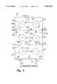
- FIG. 3there is disclosed an equivalent schematic circuit diagram of the dielectric resonator filter 18 of FIG. 2.
- a coupling factor between the plurality of resonators 26is indicated by Kij, where i, and j represent a number of a respective dielectric resonator 26.
- adjacent (in-line) resonatorshave a coupling factor with i and j in succession (e.g. K 12 ).
- non-adjacent resonatorshave a cross coupling factor where i and j are not in succession (e.g. K 16 ).
- the cross-coupling factor K 25 between dielectric resonators 2 and 5can have either a positive or a negative sign.
- the cross-coupling factor K 16' between elements 1 and 6can have either a positive or a negative sign.
- the coupling factor K 25has a negative sign while the coupling factor K 16 has a positive sign, so that the filter 18 has two transmission zeroes. Additional details as to how a positive or negative coupling factor is provided, according to the present invention, will be discussed infra.
- FIG. 5there is disclosed an equivalent schematic circuit diagram of the embodiment of the dielectric resonator filter 18, as shown in FIG. 4.
- the coupling factors K 14 and K 36can have either a positive or negative sign.
- the cross-coupling factor K 14' between non-adjacent resonators 1 and 4 and the cross-coupling factor K 36' between non-adjacent resonators 3 and 6,are both negative, so that the filter 18 has two transmission zeroes.
- the U-shaped path between the input port 20 and the output port 22, as shown in FIG. 2is used because the electrical performance of the filter 18, in the stop band, with cross-coupling factors +K 16 and -K 25' is better than an out-of-band performance with cross-coupling factors -K 14 and -K 36 of the meandered-path embodiment of FIGS. 4, 5.
- the out-of-band performance with a single reactance -K 25 ' between the second and fifth resonators, of the U-shaped path embodiment of FIGS. 2-3can be achieved with both coupling factors -K 14 and -K 36 of the meandered-path embodiment of FIGS. 4-5.
- either one of the embodiments as shown in FIGS. 2-5, as well as any modifications known to those skilled in the art,are intended to be covered by the present invention.
- a desired center frequency, a desired operating bandwidth (for example as dictated by the division of the microwave communications spectrum), a desired filter complexity and a desired return loss at the input 20 and output 22 ports,are decided upon. These parameters are used to calculate a value of Q ex' for the input port 20 and the output port 22, and the plurality of the inter-resonator coupling coefficients K ij' for a given number of dielectric resonators to be used.
- the values of Q ex and K ijcan be derived, for example, using a computer. For example, Wenzel/Erlinger Associates of Agoura Hills, Calif.
- the input parameters to the programare a lower pass-band edge frequency, an upper pass-band edge frequency, and one of a desired return loss, a desired input and output VSWR, or a desired pass band ripple (in dB).
- the useralso inputs a desired number of transmission zeroes at DC, and the transmission zero locations on the real axis and in the complex plane.
- the input/output coupling device 24includes a conductive rod 52 having a diameter d.
- a proximate end of the conductive rod 52is connected to the input port 20 or the output connector 22 at solder point 50.
- a center of the conductive rod 52is spaced, at a spacing s, from an inside of a sidewall 65 of the housing 19.
- the conductive rodhas an electrical length l 1 which can be varied by moving a conductive spacer 54 along the length of the conductive rod 52 to vary the effective wavelength of the conductive rod 52.
- the conductive spacer 54has a width w and a length l 2' and shorts a distal end of the conductive rod 52 to the sidewall 65 of the housing 19.
- the value of Q excan also be varied by varying the diameter d of the conductive rod 52 while maintaining a fixed location of the conductive spacer 54 and thus a fixed electrical length l 1 of the conductive rod. It is also to be appreciated that alternative methods of achieving Q ex' are also intended to be covered by the present invention.
- the conductive rod 52'can be an open-circuited rod instead of a short-circuited conductive rod 52.
- the distal end of the rodis not shorted to the sidewall 65 of the housing 19, but instead is an open-circuit.
- the distal end of the conductive rod, 52'is supported by a dielectric spacer 53.
- the length l 1' of the rod 52'is physically varied to achieve the desired value of Q ex .
- a diameter d' of the open-circuited rod 52'is varied, while maintaining a fixed length of the open-circuited rod 52', to achieve Q ex .
- the value of Q excan be varied by changing one of the first embodiment and the second embodiment of the input/output coupling device 24 as described above.
- modificationsreadily known to one of ordinary skill in the art, are intended to be covered by the present invention.
- tuning screws 38 and 40are provided for fine tuning of the value of Q ex .
- the tuning screwsare rotatively mounted, horizontally in a sidewall, such that an axial length of the screws are parallel to a length of the conductive rod 52.
- the tuning screwis rotated so that a proximity of a distal end of the tuning screw is varied with respect to the conductive rod 52.
- the tuning screwtunes the value of Q ex by adding capacity in parallel with shunt inductance formed by the shorted rod, to bring the resonant frequency of the parallel combination closer to the operating frequency.
- the tuning screws 38 and 40as disclosed in FIG. 1, are not so limited and that various alterations and modifications by one of ordinary skill in the art are intended to be covered by the present invention.
- the tuning screwmay be mounted in the same sidewall 65 of the housing 19, which also holds the input and output connectors 22, so that the axial length of the tuning screw is perpendicular to the length of the conductive rod 52.
- a width W I of a first iris 30can be slowly increased to achieve the desired coupling factor K 12 between, for example, the first and the second dielectric resonators 26.
- the width W I of the irisis slowly varied until a desired insertion loss response (which reflects a desired coupling factor) is measured between the respective dielectric resonators 26 of the first and the second dielectric resonator cavities 28.
- the procedure for measuring the insertion loss, between the dielectric resonatorsis readily known to those of ordinary skill in the art.
- the coupling factor K 12should be measured with the coupling tuning screw 34 in a number of positions.
- a first measurementshould be made with a distal end of the coupling tuning screw 34 flush with the sidewall of the housing 19.
- the coupling factorshould then increase (and thus the value of insertion loss should decrease) as additional measurements are made with the distal end of the coupling screw penetrating into the iris opening 30 at various distances. This is because the primary mode of coupling between the resonators is a magnetic coupling mode. Thus, as the distal end of the coupling screw 34 penetrates further into the iris 30, there should be increased inductive coupling between the resonators.
- FIG. 8illustrates a sectional view of a resonator cavity 28, taken along line A--A of FIG. 1, including resonator 26 and iris 30, having width W I' for coupling the electromagnetic field of resonator 26 to another resonator 26 in a physically adjacent resonator cavity.
- the dielectric resonator 26is mounted on a low-dielectric constant pedestal 25 having a length 1 p .
- FIG. 9illustrates the sectional view of the resonator cavity 28, takes along line A--A of FIG. 1, showing, an alternative embodiment of the iris 30' which couples the electromagnetic field from resonator 26 to another resonator 26 in the physically adjacent resonator cavity.
- the iris 30'includes a high-order mode suppression bar 31 which is substantially centered in a middle of the iris width W I .
- the suppression bar 31has a width w b which is sufficient to suppress higher-order, waveguide modes yet does not affect the inter-resonator coupling factor of the TE 01 ⁇ mode between the resonators 26.
- the iris 30 and the iris 30'can be used to provide both in-line coupling between adjacent resonators and cross-coupling between non-adjacent resonators.
- specific examples of iris configurationhave been given for providing inter-resonator coupling factors K ij between respective resonators 26, various alterations and modifications of such iris, readily known to one of ordinary skill in the art, are intended to be within the scope of the present invention.
- FIGS. 10-11there is shown a top view of alternate embodiments of mechanisms for fine tuning of the inter-resonator coupling factor K ij between respective resonators 26 of both adjacent and non-adjacent resonator cavities 28.
- these mechanismare used to fine tune the in-line coupling between respective resonators of adjacent resonator cavities.
- FIG. 10illustrates a horizontal tuning screw 34, rotatively mounted in the sidewalls of the base 19 of the filter 18.
- Each coupling factor tuning screw 34is respectively disposed so that a distal end of the tuning screw extends into a respective iris 30 between adjacent resonator cavities 28.
- the primary mode of coupling between the resonators 26 of adjacent resonator cavities 28is the magnetic coupling mode.
- the coupling tuning screw 34can be used to increase the coupling between the dielectric resonators to be greater than that which is achieved with the iris alone.
- each of the plurality of tabs 62is pivotally mounted to an end of a cavity wall 29 forming one end of the iris 30 between respective adjacent resonators cavities 28.
- each of the plurality of tabsis approximately centered with respect a height of the dielectric resonator 26 and is a fraction of the height of the cavity 28.
- Each of the plurality of tabs 62can be pivoted between a first and a second position. In a first position, an axial length of the tab is perpendicular to the cavity wall 29 such that the iris width W I is maintained. In this position the tab provides no additional magnetic coupling between adjacent resonators.
- the tab 62is pivoted into the iris 30 such that the width W I is decreased.
- the tabprovides increased inductive coupling between respective resonators 26 of the adjacent resonator cavities 28.
- the iris 30is used to provide an approximate coupling factor K ij between the respective resonators, and either a horizontal tuning screw 34 (see FIG. 10) or a tab 62 if provided to provide increased coupling between the respective dielectric resonators 26.
- FIGS. 12-13there are shown an exploded view of a plurality of devices for achieving the cross-coupling factor K ij .
- FIG. 12bshows a sectional view, taken along cutting line B--B of the top view of the Filter of FIG. 12a), of the coupling mechanism 32 and tuning screw 56.
- the coupling mechanism 32is shorted to the cover 66, through the threaded conductive spacer 58 by screw 59.
- FIG. 12cdiscloses an S-shaped loop 32, situated in an iris 60, between respective resonators of non-adjacent resonator cavities 28 (not shown herein). Using the right hand turn rule of electromagnetic field propogation, one can ascertain that the S-shaped loop provides a negative coupling -K ij between the non-adjacent resonators.
- a U-shaped loop 32'as shown in FIG. 12d), disposed in the iris 60 between non-adjacent resonators 26 (not shown herein), is used to provide a positive coupling factor +K ij between non-adjacent resonators 26.
- the S-shaped 32 and U-shaped 32' loopare provided between non-adjacent resonators to provide cross-coupling factors
- the S- and U-shaped loopscan also be disposed between adjacent, resonators to provide in-line coupling factors. More specifically the S-shaped loop 32 or the U-shaped loop 32' can be used instead of an iris 30 to provide coupling between adjacent resonators.
- FIG. 13further shows a top view of an additional mechanism for providing cross-coupling, which is a capacitive probe 32" mounted in the iris 60' between the respective resonators 26 of the non-adjacent resonator cavities 28.
- the capacitive probe 32"also provides a negative coupling factor -K ij between the non-adjacent resonators 26, and therefore can be substituted for the S-shaped loop of FIG. 11c).
- the capacitive probecan also be used to provide in-line coupling between respective resonators of adjacent resonator cavities.
- the vertical coupling tuning screw 56is vertically disposed above the coupling mechanism 32 to finely tune the coupling between the respective resonators.
- the vertical coupling tuning screw 56is mounted in the cover 66, of the dielectric resonator filter, such that a proximity of a distal end of the screw can be varied with respect to the coupling mechanism 32.
- the vertical coupling tuning screw 56provides a capacitance to ground.
- the vertical coupling tuning screw 56decreases coupling between respective resonators coupled together by the capacitive probe 32", and increases coupling between the resonators coupled together by either the U-shaped loop 32'or the S-shaped loop 32.
- these stepscan be repeated as the number of resonators in the dielectric resonator filter 18, is increased.
- a catalog of Q ex versus a varying dimension of the input/output coupling device 24,is created.
- a graphis created of Q ex as a function of varying a length of l 1 of the conductive rod 52 or a graph is created of Q ex as a function of varying the diameter d of the conductive rod 52.
- a catalog of the coupling coefficient K ijis created as a function of a varying dimension of one of the coupling devices. For example, a graph of the coupling coefficient as a function of the width W I of the iris 30, or of the coupling coefficient as a function of a dimension of the S-shaped loop 32, and the like, is created.
- the dimensions of the filter 18can then be chosen, given the output of the calculations discussed above.
- FIG. 14there is shown a sectional view, taken along cutting line B--B of FIG. 1, of the dielectric resonator 26, which is mounted on a low-dielectric pedestal 25, of the center frequency tuning screw 36 and of the conductive plate 37.
- the dielectric resonator 26is manufactured to have a certain mass, as defined by a diameter d and a thickness t of the resonator 26, minus a mass of the hole 27, having diameter d h and thickness t, so that the resonator will resonate at approximately a desired frequency range.
- the dielectric resonator 26is made of a base ceramic material having a desired dielectric constant ( ⁇ ) and a desired conductivity ( ⁇ ).
- the resonator frequency of the dielectric resonatoris also a function of ⁇ , while the Q of resonator is a function of the ⁇ (e.g. the lower the ⁇ , the higher the Q).
- a base material of the dielectric resonator 26is a high Q ZrSnTiO ceramic material having a dielectric constant ⁇ of 37.
- This base materialis doped with a first dopant Ta in a range between 50 and 1,000 parts per million (ppm). More specifically, in the preferred embodiment, 215 ppm of Ta is used as the first dopant.
- the base materialis also doped with a second dopant Sb also in a range between 50 and 1,000 ppm. More specifically, in the preferred embodiment, 165 ppm of Sb is used as the second dopant.
- the diameter of the resonatoris 29 mm
- the thicknessis 1.15 mm
- the diameter of the hole d his 7 mm.
- the mixture of Ta and Sbare used to reduce the amount of Ta used, since Sb is less expensive than Ta.
- an advantage and surprising resultis that less than a mol for mol substitution of Sb for Ta is required in order to achieve optimum performance of the dielectric resonator 26.
- an advantage of this combination of ceramic material and dopantsis that, as an operating temperature is varied, the operating frequency of the resonator 26 shifts equally in a direction opposite to that of a frequency shift due to the coefficient of thermal expansion of the housing 19. Therefore, the resonator 26 is optimized to yield a temperature stable filter 18. It is to be appreciated that although various dimensions and materials have been disclosed for the dielectric resonator, various alterations and modifications readily a to one of ordinary skill in the art, are intended to be covered by the present invention.
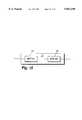
- FIG. 15is a block diagram of a band pass filter 70, according to the present invention, which will meet both in-band and out-of-band electrical performance requirements.
- the in-band electrical requirementsare for the overall filter to have less than 1.2 dB insertion loss, greater than 12 dB of return loss as well as high attenuation characteristics out-of-band.
- the PCS requirementsare greater than 93 dB of attenuation for signals at frequencies greater than 77.5 MHz from the upper and lower edges of the pass band.
- a first bandpass filter 72provides the desired pass-band of the filter 70 and also meets the in-band performance requirements.
- a second bandpass filter 74having a bandwidth greater than the bandwidth of the first bandpass filter 72, provides additional out-of-band attenuation in the stop band of the overall filter 70.
- the combination of bandpass filters 72 and 74, in series,provide both the in-band and out-of-band electrical requirements that are not necessarily achievable with a single bandpass filter 72.
- FIG. 16is a perspective view of the comb-line filter 74, which includes a plurality of resonators having equal diameter conductive rods 76, having a diameter d and a length l r centered between parallel ground planes, which are spaced by a spacing s.
- the comb-line filterhas an overall length l which must be less than 90° in the pass-band of the comb-line filter.
- the comb-line filteris chosen because a very small insertion loss can be provided in the pass-band while a steep out-of-band rejection ratio can be provided in the stop band over a broad frequency range, which can be added to the rejection ratio of the first bandpass filter 72 to meet the out-of-band electrical requirements of the filter 70.
- the first bandpass filter 72is the dielectric resonator filter 18 as discussed above.
- the dielectric resonator filter 72provides a 4 MHz pass-band centered at 1967.5 MHz and has an insertion loss of less than 0.8 dB.
- the second bandpass filter 74is a comb-line filter such as that shown in FIG. 16.
- the comb-line filter 74provides a 190 MHz pass-band centered at 1970 MHz has an insertion loss of 0.15 dB, and has an attenuation of ⁇ 93 dB at frequencies ⁇ 1890 MHz.
- the ceramic filter 72 and the comb-line filter 74combine to provide ⁇ 93 dB of the attenuation.
- the combination of the dielectric resonator filter 72 and the comb-line filter 74has an insertion loss of ⁇ 0.8 dB and an attenuation of >93 dB at frequencies ⁇ 1890 MHz and ⁇ 2045 MHz.
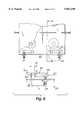
- FIG. 17there is shown a perspective view of the housing 19 and the cover 66 of the filter 18 of FIG. 1, in which there is provided a plurality of protrusions 64 and a plurality of through-holes 68 for providing a strong electrical and mechanical seal between the housing 19 and the cover 66.
- the plurality of protrusions 64 and through-holes 68provide a method and apparatus for joining the dielectric resonator filter housing 19 and the cover 66 to provide a sealed dielectric resonator filter 18 having both good electrical shielding properties and strong mechanical properties.
- the dielectric resonator filter 18maintain good electrical sealing and good mechanical stability. More specifically, any loose or incomplete contact between the base material 19 and the cover 66 may destroy the dielectric resonator filter performance by increasing filter insertion loss, reducing stop-band rejection, or creating inter-modulation products.
- the side walls 65 of the housing 19are constructed with the plurality of protrusions 64 along at least one surface of each of the sidewalls 65 and along at least one surface of each of the cavity walls 29 disposed within the base 19.
- the coveris provided with the corresponding through-holes 68 to align with the protrusions 64.
- the through-holesare circular and the protrusions are square, it is to be appreciated however that the present invention is not intended to be so limited.
- the protrusions and the through-holesmay be any combination of round, square, hexagonal, polygonal and the like.
- any alterations or modifications to the protrusions or through holesreadily known by one of ordinary skill in the art, are intended to be covered by the present invention.
- the base 19 and the cover 66are then brought into alignment.
- the base 19 and the cover 66are permanently aligned by peening each protrusion 64 over to fill the corresponding through-hole 68.
- the coveris pressed tightly to the wall, to form a tight bond that is electrically and mechanically sealed.
- a break-away side of the coverin particular a bottom side of the cover when the through-holes 66 are punched through a top of the cover, is intended to be facing up.
- the top side of the coverwhen the holes are punched through the cover, is intended to be bonded to the sidewall 65 of the base material 19.
- the protrusionsare then peened over with a high velocity, low mass force on the protrusion itself so that the protrusion expands into the through-hole.
- the top of the protrusion 64flattens into the through-hole 68 thereby pulling the cover 66 tightly against the base 19.
- the base material 19 and the cover 66are made of sheet steel.
- the round holesare punched through the cover 66 and the protrusions are punched or milled in the at least one surface of the base 19 and the cavity walls 29.
- the through-holescan also be drilled through the cover.
- other materialssuch as aluminum are also intended to be covered by the present invention.
Landscapes
- Engineering & Computer Science (AREA)
- Manufacturing & Machinery (AREA)
- Control Of Motors That Do Not Use Commutators (AREA)
Abstract
Description
Claims (33)
Priority Applications (11)
| Application Number | Priority Date | Filing Date | Title |
|---|---|---|---|
| US08/412,030US5841330A (en) | 1995-03-23 | 1995-03-23 | Series coupled filters where the first filter is a dielectric resonator filter with cross-coupling |
| CA002216158ACA2216158A1 (en) | 1995-03-23 | 1996-03-25 | Dielectric resonator filter |
| DE69613821TDE69613821T2 (en) | 1995-03-23 | 1996-03-25 | DIELECTRIC RESONATOR FILTER |
| BR9607770-0ABR9607770A (en) | 1995-03-23 | 1996-03-25 | Filter with dielectric resonator |
| AU53231/96AAU5323196A (en) | 1995-03-23 | 1996-03-25 | Dielectric resonator filter |
| PCT/US1996/004043WO1996029754A1 (en) | 1995-03-23 | 1996-03-25 | Dielectric resonator filter |
| EP96909860AEP0815612B1 (en) | 1995-03-23 | 1996-03-25 | Dielectric resonator filter |
| AT96909860TATE203125T1 (en) | 1995-03-23 | 1996-03-25 | DIELECTRIC RESONATOR FILTER |
| US09/037,408US6037541A (en) | 1995-03-23 | 1998-03-10 | Apparatus and method for forming a housing assembly |
| US09/037,908US6094113A (en) | 1995-03-23 | 1998-03-10 | Dielectric resonator filter having cross-coupled resonators |
| US09/404,872US6239673B1 (en) | 1995-03-23 | 1999-09-23 | Dielectric resonator filter having reduced spurious modes |
Applications Claiming Priority (1)
| Application Number | Priority Date | Filing Date | Title |
|---|---|---|---|
| US08/412,030US5841330A (en) | 1995-03-23 | 1995-03-23 | Series coupled filters where the first filter is a dielectric resonator filter with cross-coupling |
Related Child Applications (2)
| Application Number | Title | Priority Date | Filing Date |
|---|---|---|---|
| US09/037,908ContinuationUS6094113A (en) | 1995-03-23 | 1998-03-10 | Dielectric resonator filter having cross-coupled resonators |
| US09/037,408ContinuationUS6037541A (en) | 1995-03-23 | 1998-03-10 | Apparatus and method for forming a housing assembly |
Publications (1)
| Publication Number | Publication Date |
|---|---|
| US5841330Atrue US5841330A (en) | 1998-11-24 |
Family
ID=23631289
Family Applications (4)
| Application Number | Title | Priority Date | Filing Date |
|---|---|---|---|
| US08/412,030Expired - LifetimeUS5841330A (en) | 1995-03-23 | 1995-03-23 | Series coupled filters where the first filter is a dielectric resonator filter with cross-coupling |
| US09/037,908Expired - LifetimeUS6094113A (en) | 1995-03-23 | 1998-03-10 | Dielectric resonator filter having cross-coupled resonators |
| US09/037,408Expired - Fee RelatedUS6037541A (en) | 1995-03-23 | 1998-03-10 | Apparatus and method for forming a housing assembly |
| US09/404,872Expired - LifetimeUS6239673B1 (en) | 1995-03-23 | 1999-09-23 | Dielectric resonator filter having reduced spurious modes |
Family Applications After (3)
| Application Number | Title | Priority Date | Filing Date |
|---|---|---|---|
| US09/037,908Expired - LifetimeUS6094113A (en) | 1995-03-23 | 1998-03-10 | Dielectric resonator filter having cross-coupled resonators |
| US09/037,408Expired - Fee RelatedUS6037541A (en) | 1995-03-23 | 1998-03-10 | Apparatus and method for forming a housing assembly |
| US09/404,872Expired - LifetimeUS6239673B1 (en) | 1995-03-23 | 1999-09-23 | Dielectric resonator filter having reduced spurious modes |
Country Status (8)
| Country | Link |
|---|---|
| US (4) | US5841330A (en) |
| EP (1) | EP0815612B1 (en) |
| AT (1) | ATE203125T1 (en) |
| AU (1) | AU5323196A (en) |
| BR (1) | BR9607770A (en) |
| CA (1) | CA2216158A1 (en) |
| DE (1) | DE69613821T2 (en) |
| WO (1) | WO1996029754A1 (en) |
Cited By (69)
| Publication number | Priority date | Publication date | Assignee | Title |
|---|---|---|---|---|
| EP0977357A2 (en)* | 1998-07-28 | 2000-02-02 | Com Dev Ltd. | Low loss saw filters with non-sequential coupling and method of operation thereof |
| US6094113A (en)* | 1995-03-23 | 2000-07-25 | Bartley Machines & Manufacturing | Dielectric resonator filter having cross-coupled resonators |
| US6255919B1 (en)* | 1999-09-17 | 2001-07-03 | Com Dev Limited | Filter utilizing a coupling bar |
| US6294970B1 (en)* | 1997-12-16 | 2001-09-25 | Spinner Gmbh Elektrotechnische Fabrik | Bandpass filter |
| US6300849B1 (en)* | 1998-11-27 | 2001-10-09 | Kyocera Corporation | Distributed element filter |
| US6304160B1 (en)* | 1999-05-03 | 2001-10-16 | The Boeing Company | Coupling mechanism for and filter using TE011 and TE01δ mode resonators |
| US6317013B1 (en) | 1999-08-16 | 2001-11-13 | K & L Microwave Incorporated | Delay line filter |
| EP1162684A3 (en)* | 2000-05-23 | 2002-02-27 | Matsushita Electric Industrial Co., Ltd. | Dielectric resonator filter |
| WO2002019458A1 (en)* | 2000-08-29 | 2002-03-07 | Matsushita Electric Industrial Co., Ltd. | Dielectric filter |
| US6404307B1 (en) | 1999-12-06 | 2002-06-11 | Kathrein, Inc., Scala Division | Resonant cavity coupling mechanism |
| US6466111B1 (en) | 1999-12-06 | 2002-10-15 | Kathrein Inc., Scala Division | Coupler for resonant cavity |
| US20020180559A1 (en)* | 2001-05-31 | 2002-12-05 | Sei-Joo Jang | Dielectric resonator loaded metal cavity filter |
| US6507254B1 (en)* | 1997-09-04 | 2003-01-14 | Murata Manufacturing Co. Ltd | Multimodal dielectric resonance device, dielectric filter, composite dielectric filter, synthesizer, distributor, and communication apparatus |
| US6559740B1 (en) | 2001-12-18 | 2003-05-06 | Delta Microwave, Inc. | Tunable, cross-coupled, bandpass filter |
| US20030117241A1 (en)* | 2001-12-21 | 2003-06-26 | Radio Frequency Systems, Inc. | Adjustable capacitive coupling structure |
| US6603375B2 (en)* | 2001-07-13 | 2003-08-05 | Tyco Electronics Corp | High Q couplings of dielectric resonators to microstrip line |
| WO2004004063A1 (en)* | 2002-06-28 | 2004-01-08 | Telefonaktiebolaget L M Ericsson (Publ) | Coupling arrangement |
| US6686815B1 (en)* | 1999-08-11 | 2004-02-03 | Nokia Corporation | Microwave filter |
| US6707353B1 (en)* | 1999-11-02 | 2004-03-16 | Matsushita Electric Industrial Co., Ltd. | Dielectric filter |
| US20040051603A1 (en)* | 2002-09-17 | 2004-03-18 | Pance Kristi Dhimiter | Cross-coupled dielectric resonator circuit |
| US20040051602A1 (en)* | 2002-09-17 | 2004-03-18 | Pance Kristi Dhimiter | Dielectric resonators and circuits made therefrom |
| US6806791B1 (en) | 2000-02-29 | 2004-10-19 | Radio Frequency Systems, Inc. | Tunable microwave multiplexer |
| US20040257176A1 (en)* | 2003-05-07 | 2004-12-23 | Pance Kristi Dhimiter | Mounting mechanism for high performance dielectric resonator circuits |
| US20050200437A1 (en)* | 2004-03-12 | 2005-09-15 | M/A-Com, Inc. | Method and mechanism for tuning dielectric resonator circuits |
| US20050237135A1 (en)* | 2004-04-27 | 2005-10-27 | M/A-Com, Inc. | Slotted dielectric resonators and circuits with slotted dielectric resonators |
| US20060094471A1 (en)* | 2004-10-29 | 2006-05-04 | Michael Eddy | Dielectric loaded cavity filters for applications in proximity to the antenna |
| WO2006128510A1 (en)* | 2005-05-30 | 2006-12-07 | Matsushita Electric Industrial Co., Ltd. | Microwave filter including an end-wall coupled coaxial resonator |
| US20070090899A1 (en)* | 2005-10-24 | 2007-04-26 | M/A-Com, Inc. | Electronically tunable dielectric resonator circuits |
| US20070115080A1 (en)* | 2005-09-27 | 2007-05-24 | M/A-Com, Inc. | Dielectric resonators with axial gaps and circuits with such dielectric resonators |
| US20070159275A1 (en)* | 2006-01-12 | 2007-07-12 | M/A-Com, Inc. | Elliptical dielectric resonators and circuits with such dielectric resonators |
| US20070202920A1 (en)* | 2004-10-29 | 2007-08-30 | Antone Wireless Corporation | Low noise figure radiofrequency device |
| US20070296529A1 (en)* | 2006-06-21 | 2007-12-27 | M/A-Com, Inc. | Dielectric Resonator Circuits |
| JP2008098727A (en)* | 2006-10-06 | 2008-04-24 | Mitsubishi Electric Corp | Band pass filter |
| US7388457B2 (en) | 2005-01-20 | 2008-06-17 | M/A-Com, Inc. | Dielectric resonator with variable diameter through hole and filter with such dielectric resonators |
| US20080252399A1 (en)* | 2007-04-16 | 2008-10-16 | Eric Wiehler | Passband resonator filter with predistorted quality factor q |
| US20080272861A1 (en)* | 2007-05-02 | 2008-11-06 | M/A-Com, Inc. | Cross coupling tuning apparatus for dielectric resonator circuit |
| US20080272860A1 (en)* | 2007-05-01 | 2008-11-06 | M/A-Com, Inc. | Tunable Dielectric Resonator Circuit |
| WO2009056813A1 (en)* | 2007-10-30 | 2009-05-07 | Radio Design Limited | Tunable filter and method of use thereof |
| CN100505414C (en)* | 2006-01-04 | 2009-06-24 | 昇达科技股份有限公司 | anti-phase cross-coupler |
| WO2015017406A1 (en)* | 2013-08-01 | 2015-02-05 | Rf Micro Devices, Inc. | Tunable rf filter structure having coupled resonators |
| US20150038094A1 (en)* | 2013-08-01 | 2015-02-05 | Rf Micro Devices, Inc. | Vswr detector for a tunable filter structure |
| US20150357985A1 (en)* | 2006-11-17 | 2015-12-10 | Resonant Inc. | Low-loss tunable radio frequency filter |
| US9419578B2 (en) | 2013-06-06 | 2016-08-16 | Qorvo Us, Inc. | Tunable RF filter paths for tunable RF filter structures |
| US9444417B2 (en) | 2013-03-15 | 2016-09-13 | Qorvo Us, Inc. | Weakly coupled RF network based power amplifier architecture |
| US9628045B2 (en) | 2013-08-01 | 2017-04-18 | Qorvo Us, Inc. | Cooperative tunable RF filters |
| US9685928B2 (en) | 2013-08-01 | 2017-06-20 | Qorvo Us, Inc. | Interference rejection RF filters |
| US9705542B2 (en) | 2013-06-06 | 2017-07-11 | Qorvo Us, Inc. | Reconfigurable RF filter |
| US9705478B2 (en) | 2013-08-01 | 2017-07-11 | Qorvo Us, Inc. | Weakly coupled tunable RF receiver architecture |
| US9774311B2 (en) | 2013-03-15 | 2017-09-26 | Qorvo Us, Inc. | Filtering characteristic adjustments of weakly coupled tunable RF filters |
| US9780817B2 (en) | 2013-06-06 | 2017-10-03 | Qorvo Us, Inc. | RX shunt switching element-based RF front-end circuit |
| US9780756B2 (en) | 2013-08-01 | 2017-10-03 | Qorvo Us, Inc. | Calibration for a tunable RF filter structure |
| US9800282B2 (en) | 2013-06-06 | 2017-10-24 | Qorvo Us, Inc. | Passive voltage-gain network |
| US9825656B2 (en) | 2013-08-01 | 2017-11-21 | Qorvo Us, Inc. | Weakly coupled tunable RF transmitter architecture |
| US9859863B2 (en) | 2013-03-15 | 2018-01-02 | Qorvo Us, Inc. | RF filter structure for antenna diversity and beam forming |
| US9871499B2 (en) | 2013-03-15 | 2018-01-16 | Qorvo Us, Inc. | Multi-band impedance tuners using weakly-coupled LC resonators |
| US9899133B2 (en) | 2013-08-01 | 2018-02-20 | Qorvo Us, Inc. | Advanced 3D inductor structures with confined magnetic field |
| US9966981B2 (en) | 2013-06-06 | 2018-05-08 | Qorvo Us, Inc. | Passive acoustic resonator based RF receiver |
| US9966905B2 (en) | 2013-03-15 | 2018-05-08 | Qorvo Us, Inc. | Weakly coupled based harmonic rejection filter for feedback linearization power amplifier |
| WO2018113557A1 (en)* | 2016-12-19 | 2018-06-28 | Huawei Technologies Co., Ltd. | Method to design ceramic filters with finite transmission zeros |
| CN109119730A (en)* | 2018-08-27 | 2019-01-01 | 广东工业大学 | A kind of TM based on capacitive load010The base station filters of dielectric resonant chamber |
| CN111490319A (en)* | 2019-01-29 | 2020-08-04 | 苏州艾福电子通讯股份有限公司 | Microwave filter |
| US10796835B2 (en) | 2015-08-24 | 2020-10-06 | Qorvo Us, Inc. | Stacked laminate inductors for high module volume utilization and performance-cost-size-processing-time tradeoff |
| CN113036350A (en)* | 2019-12-25 | 2021-06-25 | 深圳市大富科技股份有限公司 | Communication device and filter thereof |
| US11139238B2 (en) | 2016-12-07 | 2021-10-05 | Qorvo Us, Inc. | High Q factor inductor structure |
| CN113675567A (en)* | 2020-05-15 | 2021-11-19 | 大富科技(安徽)股份有限公司 | A filter and communication equipment |
| WO2022019041A1 (en)* | 2020-07-22 | 2022-01-27 | 株式会社村田製作所 | Band-pass filter and high-frequency front-end circuit comprising same |
| EP3913734A4 (en)* | 2019-01-17 | 2022-09-07 | Rosenberger Technology (Kunshan) Co., Ltd. | Single-layer cross-coupled filter |
| JP2024531708A (en)* | 2021-09-14 | 2024-08-29 | テレフオンアクチーボラゲット エルエム エリクソン(パブル) | Integrated low-pass and band-pass filter units formed by sheet metal coated with a dielectric material |
| US12224096B2 (en) | 2013-03-15 | 2025-02-11 | Qorvo Us, Inc. | Advanced 3D inductor structures with confined magnetic field |
Families Citing this family (55)
| Publication number | Priority date | Publication date | Assignee | Title |
|---|---|---|---|---|
| DE19633727C1 (en)* | 1996-08-21 | 1997-09-18 | Siemens Ag | Electrical component e.g. automobile relay and switch-relay for FAO |
| CA2231033A1 (en)* | 1997-04-11 | 1998-10-11 | Jose Luis Caceres Armendariz | Microwave filter with coupling elements |
| JP3991390B2 (en)* | 1997-05-30 | 2007-10-17 | 富士通株式会社 | Storage device |
| US6314000B1 (en) | 1998-08-27 | 2001-11-06 | Lucent Technologies Inc. | Enclosure for an RF assembly |
| EP1017122A3 (en)* | 1998-12-28 | 2003-05-28 | Alcatel | Microwave equaliser with internal amplitude correction |
| JP3567827B2 (en)* | 1999-11-02 | 2004-09-22 | 株式会社村田製作所 | Dielectric filter, composite dielectric filter, dielectric duplexer, dielectric diplexer, and communication device |
| DE10034338C2 (en)* | 2000-07-14 | 2002-06-20 | Forschungszentrum Juelich Gmbh | Multipole cascading quadruple bandpass filter based on dielectric dual-mode resonators |
| US6555743B1 (en)* | 2000-08-04 | 2003-04-29 | Dell Products L.P. | EMI attenuation obtained by application of waveguide beyond frequency cutoff techniques for add-in ITE mass storage devices |
| SE0004935D0 (en)* | 2000-12-29 | 2000-12-29 | Allgon Ab | A filter including coaxial cavity resonators |
| ITSO20010002A1 (en)* | 2001-05-18 | 2002-11-18 | Comtech S R L | MINIMUM ORDER FILTER WITH CAVITY COUPLED FOR UHF TELEVISION CHANNELS. |
| US6627810B2 (en)* | 2001-06-19 | 2003-09-30 | Honeywell International Inc. | Magnetic shield for optical gyroscopes |
| US6627812B2 (en)* | 2001-08-24 | 2003-09-30 | Sun Microsystems, Inc. | Apparatus for containing electro-magnetic interference |
| JP3915536B2 (en)* | 2002-02-12 | 2007-05-16 | 住友電装株式会社 | Hood release lever mounting structure |
| DE10208666A1 (en)* | 2002-02-28 | 2003-09-04 | Marconi Comm Gmbh | Bandpass filter with parallel signal paths |
| EP1372211A3 (en)* | 2002-06-12 | 2004-01-07 | Matsushita Electric Industrial Co., Ltd. | Dielectric filter, communication apparatus, and method of controlling resonance frequency |
| CH696098A5 (en)* | 2002-12-11 | 2006-12-15 | Thales Suisse Sa | Tunable high-frequency filter assembly as well as methods for their preparation. |
| DE10304524A1 (en)* | 2003-02-04 | 2004-08-12 | Tesat-Spacecom Gmbh & Co.Kg | Band-pass filter topology e.g. for satellite communication transponders, has coupling to first resonator and decoupling from resonator lying opposite this in rectangular structure |
| EP1465283A1 (en)* | 2003-04-04 | 2004-10-06 | Alcatel | Dielectric resonator filter |
| US7075392B2 (en)* | 2003-10-06 | 2006-07-11 | Com Dev Ltd. | Microwave resonator and filter assembly |
| US20050088068A1 (en)* | 2003-10-22 | 2005-04-28 | Lin-Wei Chang | Server rack |
| TWI271027B (en)* | 2005-02-14 | 2007-01-11 | Wistron Neweb Corp | LNBF and shielding structure thereof |
| US20080093099A1 (en)* | 2006-10-16 | 2008-04-24 | Alcan International Limited | Electrical Box Ring and Method for Manufacturing The Same |
| CA2609625A1 (en)* | 2007-09-10 | 2009-03-10 | Veris Industries, Llc | Multi-voltage housing |
| US7764146B2 (en)* | 2008-06-13 | 2010-07-27 | Com Dev International Ltd. | Cavity microwave filter assembly with lossy networks |
| EP2319120A1 (en) | 2008-08-12 | 2011-05-11 | Lockheed Martin Corporation | Mode suppression resonator |
| ITMI20082018A1 (en)* | 2008-11-14 | 2010-05-15 | Abf Elettronica Srl | HIGH FREQUENCY SIGNAL FILTERS REMOVABLE, ASSEMBLED AND MANUFACTURING METHOD |
| CN101728614B (en)* | 2010-01-07 | 2013-09-18 | 东莞市高鑫机电科技服务有限公司 | A signal attenuation control method and cross-coupling structure |
| KR101033505B1 (en)* | 2010-12-29 | 2011-05-09 | 주식회사 이너트론 | Microstrip Line Filters with Ground Rails |
| KR20130015933A (en) | 2011-08-05 | 2013-02-14 | 주식회사 케이엠더블유 | Radio frequency filter with notch structure |
| US8907742B2 (en)* | 2012-04-09 | 2014-12-09 | Space Systems/Loral, Llc | Electrostatic discharge control for a multi-cavity microwave filter |
| US9178487B2 (en) | 2013-06-28 | 2015-11-03 | Nokia Technologies Oy | Methods and apparatus for signal filtering |
| EP2897214A1 (en)* | 2014-01-17 | 2015-07-22 | Alcatel Lucent | A bandwidth tunable filter and a method for constructing and tuning such a filter |
| US10122478B2 (en)* | 2015-02-27 | 2018-11-06 | Purdue Research Foundation | Methods and devices for real-time monitoring of tunable filters |
| KR101677950B1 (en)* | 2015-04-13 | 2016-11-21 | 주식회사 에이스테크놀로지 | Cavity filter using cross-coupling |
| GB2540007A (en)* | 2015-04-28 | 2017-01-04 | Rhodes David | A tuneable microwave filter and a tuneable microwave multiplexer |
| US9951934B2 (en) | 2016-03-17 | 2018-04-24 | Elemental LED, Inc. | Junction box for LED drivers |
| RU2645033C1 (en)* | 2017-04-05 | 2018-02-15 | Общество с ограниченной ответственностью Научно-производственное предприятие "НИКА-СВЧ" | Microwave multiplexer |
| US10116127B1 (en) | 2017-12-12 | 2018-10-30 | Elemental LED, Inc. | Junction boxes with wrap-around compartments |
| EP3797447A4 (en)* | 2018-06-04 | 2022-01-05 | Nokia Solutions and Networks Oy | A cavity filter |
| CN109037861B (en) | 2018-06-05 | 2019-12-06 | 深圳三星通信技术研究有限公司 | A dielectric waveguide filter |
| CN111786069B (en) | 2019-04-04 | 2021-09-21 | 上海诺基亚贝尔股份有限公司 | Resonator and filter |
| US10622794B1 (en) | 2019-04-25 | 2020-04-14 | Elemental LED, Inc. | Electrical gang box with integrated driver |
| US10855065B1 (en) | 2019-12-04 | 2020-12-01 | Elemental LED, Inc. | Weather-resistant junction box |
| CN113036353A (en)* | 2019-12-25 | 2021-06-25 | 深圳市大富科技股份有限公司 | Filter and communication equipment |
| CN113036349A (en)* | 2019-12-25 | 2021-06-25 | 深圳市大富科技股份有限公司 | Filter and communication equipment |
| CN113036345A (en)* | 2019-12-25 | 2021-06-25 | 深圳市大富科技股份有限公司 | Communication system and filter thereof |
| RU197717U1 (en)* | 2020-01-29 | 2020-05-25 | Акционерное общество «Российская корпорация ракетно-космического приборостроения и информационных систем» (АО «Российские космические системы») | Microwave filter |
| CN113571857A (en)* | 2020-04-28 | 2021-10-29 | 深圳市大富科技股份有限公司 | Filter and communication equipment |
| US11317502B2 (en) | 2020-05-15 | 2022-04-26 | Raytheon Company | PCB cavity mode suppression |
| CN113851802A (en)* | 2020-06-28 | 2021-12-28 | 大富科技(安徽)股份有限公司 | Filter and communication equipment |
| CN113851803A (en)* | 2020-06-28 | 2021-12-28 | 大富科技(安徽)股份有限公司 | Filter and communication equipment |
| CN113922024A (en)* | 2020-07-09 | 2022-01-11 | 大富科技(安徽)股份有限公司 | Filter and communication equipment |
| CN112436255B (en)* | 2020-10-26 | 2021-10-26 | 华信咨询设计研究院有限公司 | anti-5G base station interference filter |
| CN112599944A (en)* | 2020-11-30 | 2021-04-02 | 湖南迈克森伟电子科技有限公司 | Miniaturized high-suppression adjustable cavity filter |
| CN113410603B (en)* | 2021-06-16 | 2022-08-02 | 聪微科技(深圳)有限公司 | Microwave filter and manufacturing method thereof |
Citations (23)
| Publication number | Priority date | Publication date | Assignee | Title |
|---|---|---|---|---|
| US2637782A (en)* | 1947-11-28 | 1953-05-05 | Motorola Inc | Resonant cavity filter |
| DE1010595B (en)* | 1956-03-17 | 1957-06-19 | Pintsch Electro Gmbh | Arrangement for coupling a coaxial power line to a rectangular waveguide to excite the H-wave |
| DE967797C (en)* | 1951-01-17 | 1957-12-12 | Siemens Ag | Arrangement for achieving an adjustable coupling between high-frequency arrangements, in particular high-frequency lines |
| DE1029435B (en)* | 1957-03-15 | 1958-05-08 | Siemens Ag | Constructive formation of an adjustable loop coupling |
| US2995806A (en)* | 1957-10-08 | 1961-08-15 | Gen Electric Co Ltd | Methods of manufacturing waveguides |
| US3124768A (en)* | 1964-03-10 | Resonator | ||
| DE1942909A1 (en)* | 1969-08-22 | 1971-03-04 | Siemens Ag | Filter for very short electromagnetic waves |
| DE1942867A1 (en)* | 1969-08-22 | 1971-03-04 | Siemens Ag | Filter for very short electromagnetic waves |
| DE2040495A1 (en)* | 1970-08-14 | 1972-02-17 | Licentia Gmbh | Filter arrangement consisting of a multi-circuit waveguide filter |
| US3737816A (en)* | 1970-09-15 | 1973-06-05 | Standard Telephones Cables Ltd | Rectangular cavity resonator and microwave filters built from such resonators |
| US3899756A (en)* | 1973-05-05 | 1975-08-12 | Marconi Co Ltd | Microwave phase correcting network utilizing waveguide coupler having mismatched ports caused by laterally displaced end section |
| JPS54103655A (en)* | 1978-02-01 | 1979-08-15 | Nec Corp | Microwave band pass filter |
| US4291288A (en)* | 1979-12-10 | 1981-09-22 | Hughes Aircraft Company | Folded end-coupled general response filter |
| DE3041625A1 (en)* | 1980-11-05 | 1982-06-09 | Standard Elektrik Lorenz Ag, 7000 Stuttgart | MICROWAVE FILTER |
| EP0101369A1 (en)* | 1982-08-10 | 1984-02-22 | Alcatel Thomson Faisceaux Hertziens | Band-pass filter with dielectric resonators presenting negative coupling between resonators |
| US4453146A (en)* | 1982-09-27 | 1984-06-05 | Ford Aerospace & Communications Corporation | Dual-mode dielectric loaded cavity filter with nonadjacent mode couplings |
| US4477785A (en)* | 1981-12-02 | 1984-10-16 | Communications Satellite Corporation | Generalized dielectric resonator filter |
| US4761624A (en)* | 1986-08-08 | 1988-08-02 | Alps Electric Co., Ltd. | Microwave band-pass filter |
| US4821006A (en)* | 1987-01-17 | 1989-04-11 | Murata Manufacturing Co., Ltd. | Dielectric resonator apparatus |
| EP0336675A1 (en)* | 1988-04-05 | 1989-10-11 | Com Dev Ltd. | Dielectric image-resonator multiplexer |
| JPH0555857A (en)* | 1991-08-27 | 1993-03-05 | Murata Mfg Co Ltd | Filter circuit |
| US5220300A (en)* | 1992-04-15 | 1993-06-15 | Rs Microwave Company, Inc. | Resonator filters with wide stopbands |
| US5608363A (en)* | 1994-04-01 | 1997-03-04 | Com Dev Ltd. | Folded single mode dielectric resonator filter with cross couplings between non-sequential adjacent resonators and cross diagonal couplings between non-sequential contiguous resonators |
Family Cites Families (14)
| Publication number | Priority date | Publication date | Assignee | Title |
|---|---|---|---|---|
| US3010199A (en)* | 1955-02-24 | 1961-11-28 | Smith | Tool and method for securing sheet metal pieces together |
| US3774799A (en)* | 1971-11-03 | 1973-11-27 | Gen Am Transport | Sectional floating roof and method of forming same |
| US3899759A (en)* | 1974-04-08 | 1975-08-12 | Microwave Ass | Electric wave resonators |
| DE3411914C1 (en)* | 1984-03-30 | 1985-08-22 | Siemens AG, 1000 Berlin und 8000 München | Device for connecting wall elements, for printing blocks in printing devices |
| JPS63500134A (en)* | 1985-07-08 | 1988-01-14 | スペイス・システムズ・ローラル・インコーポレイテッド | Narrowband bandpass dielectric resonator filter |
| JPH01260901A (en)* | 1988-04-11 | 1989-10-18 | Fujitsu Ltd | Dielectric filter |
| JPH0277302A (en)* | 1988-06-17 | 1990-03-16 | Sugino Techno:Kk | Wheel and disc body used for it |
| JPH0237801A (en)* | 1988-07-27 | 1990-02-07 | Nippon Dengiyou Kosaku Kk | Band-pass filter |
| JPH02277302A (en) | 1989-04-18 | 1990-11-13 | Fujitsu Ltd | Magnetic field coupling loop |
| JPH036099A (en)* | 1989-06-02 | 1991-01-11 | Canon Inc | Mounting structure of electronic equipment |
| US5032807A (en)* | 1989-07-10 | 1991-07-16 | General Instrument Corporation | Notch filter using helical transmission line and coaxial capacitor |
| US5175395A (en)* | 1991-11-27 | 1992-12-29 | Rockwell International Corporation | Electromagnetic shield |
| WO1995027317A2 (en)* | 1994-04-01 | 1995-10-12 | Com Dev Ltd | Dielectric resonator filter |
| US5841330A (en)* | 1995-03-23 | 1998-11-24 | Bartley Machines & Manufacturing | Series coupled filters where the first filter is a dielectric resonator filter with cross-coupling |
- 1995
- 1995-03-23USUS08/412,030patent/US5841330A/ennot_activeExpired - Lifetime
- 1996
- 1996-03-25CACA002216158Apatent/CA2216158A1/ennot_activeAbandoned
- 1996-03-25WOPCT/US1996/004043patent/WO1996029754A1/enactiveIP Right Grant
- 1996-03-25ATAT96909860Tpatent/ATE203125T1/ennot_activeIP Right Cessation
- 1996-03-25DEDE69613821Tpatent/DE69613821T2/ennot_activeExpired - Fee Related
- 1996-03-25EPEP96909860Apatent/EP0815612B1/ennot_activeExpired - Lifetime
- 1996-03-25BRBR9607770-0Apatent/BR9607770A/ennot_activeIP Right Cessation
- 1996-03-25AUAU53231/96Apatent/AU5323196A/ennot_activeAbandoned
- 1998
- 1998-03-10USUS09/037,908patent/US6094113A/ennot_activeExpired - Lifetime
- 1998-03-10USUS09/037,408patent/US6037541A/ennot_activeExpired - Fee Related
- 1999
- 1999-09-23USUS09/404,872patent/US6239673B1/ennot_activeExpired - Lifetime
Patent Citations (23)
| Publication number | Priority date | Publication date | Assignee | Title |
|---|---|---|---|---|
| US3124768A (en)* | 1964-03-10 | Resonator | ||
| US2637782A (en)* | 1947-11-28 | 1953-05-05 | Motorola Inc | Resonant cavity filter |
| DE967797C (en)* | 1951-01-17 | 1957-12-12 | Siemens Ag | Arrangement for achieving an adjustable coupling between high-frequency arrangements, in particular high-frequency lines |
| DE1010595B (en)* | 1956-03-17 | 1957-06-19 | Pintsch Electro Gmbh | Arrangement for coupling a coaxial power line to a rectangular waveguide to excite the H-wave |
| DE1029435B (en)* | 1957-03-15 | 1958-05-08 | Siemens Ag | Constructive formation of an adjustable loop coupling |
| US2995806A (en)* | 1957-10-08 | 1961-08-15 | Gen Electric Co Ltd | Methods of manufacturing waveguides |
| DE1942909A1 (en)* | 1969-08-22 | 1971-03-04 | Siemens Ag | Filter for very short electromagnetic waves |
| DE1942867A1 (en)* | 1969-08-22 | 1971-03-04 | Siemens Ag | Filter for very short electromagnetic waves |
| DE2040495A1 (en)* | 1970-08-14 | 1972-02-17 | Licentia Gmbh | Filter arrangement consisting of a multi-circuit waveguide filter |
| US3737816A (en)* | 1970-09-15 | 1973-06-05 | Standard Telephones Cables Ltd | Rectangular cavity resonator and microwave filters built from such resonators |
| US3899756A (en)* | 1973-05-05 | 1975-08-12 | Marconi Co Ltd | Microwave phase correcting network utilizing waveguide coupler having mismatched ports caused by laterally displaced end section |
| JPS54103655A (en)* | 1978-02-01 | 1979-08-15 | Nec Corp | Microwave band pass filter |
| US4291288A (en)* | 1979-12-10 | 1981-09-22 | Hughes Aircraft Company | Folded end-coupled general response filter |
| DE3041625A1 (en)* | 1980-11-05 | 1982-06-09 | Standard Elektrik Lorenz Ag, 7000 Stuttgart | MICROWAVE FILTER |
| US4477785A (en)* | 1981-12-02 | 1984-10-16 | Communications Satellite Corporation | Generalized dielectric resonator filter |
| EP0101369A1 (en)* | 1982-08-10 | 1984-02-22 | Alcatel Thomson Faisceaux Hertziens | Band-pass filter with dielectric resonators presenting negative coupling between resonators |
| US4453146A (en)* | 1982-09-27 | 1984-06-05 | Ford Aerospace & Communications Corporation | Dual-mode dielectric loaded cavity filter with nonadjacent mode couplings |
| US4761624A (en)* | 1986-08-08 | 1988-08-02 | Alps Electric Co., Ltd. | Microwave band-pass filter |
| US4821006A (en)* | 1987-01-17 | 1989-04-11 | Murata Manufacturing Co., Ltd. | Dielectric resonator apparatus |
| EP0336675A1 (en)* | 1988-04-05 | 1989-10-11 | Com Dev Ltd. | Dielectric image-resonator multiplexer |
| JPH0555857A (en)* | 1991-08-27 | 1993-03-05 | Murata Mfg Co Ltd | Filter circuit |
| US5220300A (en)* | 1992-04-15 | 1993-06-15 | Rs Microwave Company, Inc. | Resonator filters with wide stopbands |
| US5608363A (en)* | 1994-04-01 | 1997-03-04 | Com Dev Ltd. | Folded single mode dielectric resonator filter with cross couplings between non-sequential adjacent resonators and cross diagonal couplings between non-sequential contiguous resonators |
Non-Patent Citations (11)
| Title |
|---|
| D. Kaifez and P., Guillon "Dielectric Resonators"©1990 by Vector Fields P.O. Box 757, University, Mississippi 38677,pp. 459-463. |
| D. Kaifez and P., Guillon Dielectric Resonators 1990 by Vector Fields P.O. Box 757, University, Mississippi 38677,pp. 459 463.* |
| PCT WO 87/00350 Ford Aerospace & Communications Corp., p.1, line 8 line 17, p. 7, line 25 line 28; fig. 1 Jan. 15, 1987.* |
| PCT WO 87/00350 Ford Aerospace & Communications Corp., p.1, line 8-line 17, p. 7, line 25-line 28; fig. 1 Jan. 15, 1987. |
| PCT WO 95/27317 Com Dev LTD., p. 9, line 19 p. 10, line 4, p. 13, line1 p. 14. line 17; fig. 2A, 2B, 5A 8, Oct. 12, 1995.* |
| PCT WO 95/27317 Com Dev LTD., p. 9, line 19-p. 10, line 4, p. 13, line1-p. 14. line 17; fig. 2A, 2B, 5A-8, Oct. 12, 1995. |
| PCT/US 96/04043 Communication Relating to the Results of the Partial International Search.* |
| V. Madrangeas et al. "Analysis and Realization of L-Band Dielectric Resonator Microwave Filters", IEEE Transactions on Microwave Theory and Techniques, vol. 40, No. 1, Jan. 1992, New York. |
| V. Madrangeas et al. Analysis and Realization of L Band Dielectric Resonator Microwave Filters , IEEE Transactions on Microwave Theory and Techniques, vol. 40, No. 1, Jan. 1992, New York.* |
| Y. Kobavashi et al, "Elliptic bandpass filters using four TM010 Dielectric Rod Resonators", 1986 IEEE-MTT-S International Microwave Symposium Digest, pp. 353-356, XP002005095 Jun. 2-4, 1986. |
| Y. Kobavashi et al, Elliptic bandpass filters using four TM 010 Dielectric Rod Resonators , 1986 IEEE MTT S International Microwave Symposium Digest, pp. 353 356, XP002005095 Jun. 2 4, 1986.* |
Cited By (115)
| Publication number | Priority date | Publication date | Assignee | Title |
|---|---|---|---|---|
| US6094113A (en)* | 1995-03-23 | 2000-07-25 | Bartley Machines & Manufacturing | Dielectric resonator filter having cross-coupled resonators |
| US6239673B1 (en)* | 1995-03-23 | 2001-05-29 | Bartley Machines & Manufacturing | Dielectric resonator filter having reduced spurious modes |
| US6507254B1 (en)* | 1997-09-04 | 2003-01-14 | Murata Manufacturing Co. Ltd | Multimodal dielectric resonance device, dielectric filter, composite dielectric filter, synthesizer, distributor, and communication apparatus |
| US6294970B1 (en)* | 1997-12-16 | 2001-09-25 | Spinner Gmbh Elektrotechnische Fabrik | Bandpass filter |
| EP0977357A2 (en)* | 1998-07-28 | 2000-02-02 | Com Dev Ltd. | Low loss saw filters with non-sequential coupling and method of operation thereof |
| US6300849B1 (en)* | 1998-11-27 | 2001-10-09 | Kyocera Corporation | Distributed element filter |
| US6304160B1 (en)* | 1999-05-03 | 2001-10-16 | The Boeing Company | Coupling mechanism for and filter using TE011 and TE01δ mode resonators |
| US6686815B1 (en)* | 1999-08-11 | 2004-02-03 | Nokia Corporation | Microwave filter |
| US6317013B1 (en) | 1999-08-16 | 2001-11-13 | K & L Microwave Incorporated | Delay line filter |
| US6255919B1 (en)* | 1999-09-17 | 2001-07-03 | Com Dev Limited | Filter utilizing a coupling bar |
| US6707353B1 (en)* | 1999-11-02 | 2004-03-16 | Matsushita Electric Industrial Co., Ltd. | Dielectric filter |
| US6404307B1 (en) | 1999-12-06 | 2002-06-11 | Kathrein, Inc., Scala Division | Resonant cavity coupling mechanism |
| US6466111B1 (en) | 1999-12-06 | 2002-10-15 | Kathrein Inc., Scala Division | Coupler for resonant cavity |
| US6806791B1 (en) | 2000-02-29 | 2004-10-19 | Radio Frequency Systems, Inc. | Tunable microwave multiplexer |
| US6700461B2 (en) | 2000-05-23 | 2004-03-02 | Matsushita Electric Industrial Co., Ltd. | Dielectric resonator filter |
| US6861928B2 (en) | 2000-05-23 | 2005-03-01 | Matsushita Electric Industrial Co., Ltd. | Dielectric resonator filter |
| US6771146B2 (en) | 2000-05-23 | 2004-08-03 | Matsushita Electric Industrial Co., Ltd. | Dielectric resonator filter |
| US6642815B2 (en) | 2000-05-23 | 2003-11-04 | Matsushita Electric Industrial Co., Ltd. | Dielectric resonator filter |
| EP1427052A3 (en)* | 2000-05-23 | 2005-11-30 | Matsushita Electric Industrial Co., Ltd. | Dielectric resonator filter |
| EP1162684A3 (en)* | 2000-05-23 | 2002-02-27 | Matsushita Electric Industrial Co., Ltd. | Dielectric resonator filter |
| US20040021533A1 (en)* | 2000-05-23 | 2004-02-05 | Yasunao Okazaki | Dielectric resonator filter |
| US20040029540A1 (en)* | 2000-05-23 | 2004-02-12 | Yasunao Okazaki | Dielectric resonator filter |
| WO2002019458A1 (en)* | 2000-08-29 | 2002-03-07 | Matsushita Electric Industrial Co., Ltd. | Dielectric filter |
| EP1315228A4 (en)* | 2000-08-29 | 2004-03-17 | Matsushita Electric Industrial Co Ltd | DIELECTRIC FILTER |
| US6975181B2 (en) | 2001-05-31 | 2005-12-13 | Sei-Joo Jang | Dielectric resonator loaded metal cavity filter |
| US20020180559A1 (en)* | 2001-05-31 | 2002-12-05 | Sei-Joo Jang | Dielectric resonator loaded metal cavity filter |
| US6603375B2 (en)* | 2001-07-13 | 2003-08-05 | Tyco Electronics Corp | High Q couplings of dielectric resonators to microstrip line |
| US6559740B1 (en) | 2001-12-18 | 2003-05-06 | Delta Microwave, Inc. | Tunable, cross-coupled, bandpass filter |
| US20030117241A1 (en)* | 2001-12-21 | 2003-06-26 | Radio Frequency Systems, Inc. | Adjustable capacitive coupling structure |
| US6836198B2 (en) | 2001-12-21 | 2004-12-28 | Radio Frequency Systems, Inc. | Adjustable capacitive coupling structure |
| WO2004004063A1 (en)* | 2002-06-28 | 2004-01-08 | Telefonaktiebolaget L M Ericsson (Publ) | Coupling arrangement |
| US20050200435A1 (en)* | 2002-09-17 | 2005-09-15 | M/A-Com, Inc. | Cross-coupled dielectric resonator circuit |
| US20040051602A1 (en)* | 2002-09-17 | 2004-03-18 | Pance Kristi Dhimiter | Dielectric resonators and circuits made therefrom |
| US7310031B2 (en) | 2002-09-17 | 2007-12-18 | M/A-Com, Inc. | Dielectric resonators and circuits made therefrom |
| US7183881B2 (en) | 2002-09-17 | 2007-02-27 | M/A-Com, Inc. | Cross-coupled dielectric resonator circuit |
| US20040051603A1 (en)* | 2002-09-17 | 2004-03-18 | Pance Kristi Dhimiter | Cross-coupled dielectric resonator circuit |
| US20040257176A1 (en)* | 2003-05-07 | 2004-12-23 | Pance Kristi Dhimiter | Mounting mechanism for high performance dielectric resonator circuits |
| US20050200437A1 (en)* | 2004-03-12 | 2005-09-15 | M/A-Com, Inc. | Method and mechanism for tuning dielectric resonator circuits |
| US20060197631A1 (en)* | 2004-03-12 | 2006-09-07 | M/A-Com, Inc. | Method and mechanism for tuning dielectric resonator circuits |
| US7352263B2 (en) | 2004-03-12 | 2008-04-01 | M/A-Com, Inc. | Method and mechanism for tuning dielectric resonator circuits |
| US20050237135A1 (en)* | 2004-04-27 | 2005-10-27 | M/A-Com, Inc. | Slotted dielectric resonators and circuits with slotted dielectric resonators |
| US20060238276A1 (en)* | 2004-04-27 | 2006-10-26 | Pance Kristi D | Slotted dielectric resonators and circuits with slotted dielectric resonators |
| US7088203B2 (en) | 2004-04-27 | 2006-08-08 | M/A-Com, Inc. | Slotted dielectric resonators and circuits with slotted dielectric resonators |
| US20060094471A1 (en)* | 2004-10-29 | 2006-05-04 | Michael Eddy | Dielectric loaded cavity filters for applications in proximity to the antenna |
| US7738853B2 (en) | 2004-10-29 | 2010-06-15 | Antone Wireless Corporation | Low noise figure radiofrequency device |
| US20070202920A1 (en)* | 2004-10-29 | 2007-08-30 | Antone Wireless Corporation | Low noise figure radiofrequency device |
| US7457640B2 (en) | 2004-10-29 | 2008-11-25 | Antone Wireless Corporation | Dielectric loaded cavity filters for non-actively cooled applications in proximity to the antenna |
| US7388457B2 (en) | 2005-01-20 | 2008-06-17 | M/A-Com, Inc. | Dielectric resonator with variable diameter through hole and filter with such dielectric resonators |
| EP1732158A1 (en)* | 2005-05-30 | 2006-12-13 | Matsushita Electric Industrial Co., Ltd. | Microwave filter including an end-wall coupled coaxial resonator |
| WO2006128510A1 (en)* | 2005-05-30 | 2006-12-07 | Matsushita Electric Industrial Co., Ltd. | Microwave filter including an end-wall coupled coaxial resonator |
| US20080122559A1 (en)* | 2005-05-30 | 2008-05-29 | Michael Hoft | Microwave Filter Including an End-Wall Coupled Coaxial Resonator |
| US20070115080A1 (en)* | 2005-09-27 | 2007-05-24 | M/A-Com, Inc. | Dielectric resonators with axial gaps and circuits with such dielectric resonators |
| US7583164B2 (en) | 2005-09-27 | 2009-09-01 | Kristi Dhimiter Pance | Dielectric resonators with axial gaps and circuits with such dielectric resonators |
| US20070090899A1 (en)* | 2005-10-24 | 2007-04-26 | M/A-Com, Inc. | Electronically tunable dielectric resonator circuits |
| US7352264B2 (en) | 2005-10-24 | 2008-04-01 | M/A-Com, Inc. | Electronically tunable dielectric resonator circuits |
| CN100505414C (en)* | 2006-01-04 | 2009-06-24 | 昇达科技股份有限公司 | anti-phase cross-coupler |
| US7705694B2 (en) | 2006-01-12 | 2010-04-27 | Cobham Defense Electronic Systems Corporation | Rotatable elliptical dielectric resonators and circuits with such dielectric resonators |
| US20070159275A1 (en)* | 2006-01-12 | 2007-07-12 | M/A-Com, Inc. | Elliptical dielectric resonators and circuits with such dielectric resonators |
| US7719391B2 (en) | 2006-06-21 | 2010-05-18 | Cobham Defense Electronic Systems Corporation | Dielectric resonator circuits |
| US20070296529A1 (en)* | 2006-06-21 | 2007-12-27 | M/A-Com, Inc. | Dielectric Resonator Circuits |
| JP2008098727A (en)* | 2006-10-06 | 2008-04-24 | Mitsubishi Electric Corp | Band pass filter |
| US9647628B2 (en)* | 2006-11-17 | 2017-05-09 | Resonant Inc. | Low-loss tunable radio frequency filter |
| US9787283B2 (en) | 2006-11-17 | 2017-10-10 | Resonant Inc. | Low-loss tunable radio frequency filter |
| US20150357985A1 (en)* | 2006-11-17 | 2015-12-10 | Resonant Inc. | Low-loss tunable radio frequency filter |
| US10027310B2 (en) | 2006-11-17 | 2018-07-17 | Resonant Inc. | Low-loss tunable radio frequency filter |
| US9647627B2 (en)* | 2006-11-17 | 2017-05-09 | Resonant Inc. | Low-loss tunable radio frequency filter |
| US20160028361A1 (en)* | 2006-11-17 | 2016-01-28 | Resonant Inc. | Low-loss tunable radio frequency filter |
| US20080252399A1 (en)* | 2007-04-16 | 2008-10-16 | Eric Wiehler | Passband resonator filter with predistorted quality factor q |
| US7782158B2 (en)* | 2007-04-16 | 2010-08-24 | Andrew Llc | Passband resonator filter with predistorted quality factor Q |
| US20080272860A1 (en)* | 2007-05-01 | 2008-11-06 | M/A-Com, Inc. | Tunable Dielectric Resonator Circuit |
| US7456712B1 (en) | 2007-05-02 | 2008-11-25 | Cobham Defense Electronics Corporation | Cross coupling tuning apparatus for dielectric resonator circuit |
| US20080272861A1 (en)* | 2007-05-02 | 2008-11-06 | M/A-Com, Inc. | Cross coupling tuning apparatus for dielectric resonator circuit |
| WO2009056813A1 (en)* | 2007-10-30 | 2009-05-07 | Radio Design Limited | Tunable filter and method of use thereof |
| US12224096B2 (en) | 2013-03-15 | 2025-02-11 | Qorvo Us, Inc. | Advanced 3D inductor structures with confined magnetic field |
| US9966905B2 (en) | 2013-03-15 | 2018-05-08 | Qorvo Us, Inc. | Weakly coupled based harmonic rejection filter for feedback linearization power amplifier |
| US9859863B2 (en) | 2013-03-15 | 2018-01-02 | Qorvo Us, Inc. | RF filter structure for antenna diversity and beam forming |
| US9774311B2 (en) | 2013-03-15 | 2017-09-26 | Qorvo Us, Inc. | Filtering characteristic adjustments of weakly coupled tunable RF filters |
| US11190149B2 (en) | 2013-03-15 | 2021-11-30 | Qorvo Us, Inc. | Weakly coupled based harmonic rejection filter for feedback linearization power amplifier |
| US9444417B2 (en) | 2013-03-15 | 2016-09-13 | Qorvo Us, Inc. | Weakly coupled RF network based power amplifier architecture |
| US11177064B2 (en) | 2013-03-15 | 2021-11-16 | Qorvo Us, Inc. | Advanced 3D inductor structures with confined magnetic field |
| US9871499B2 (en) | 2013-03-15 | 2018-01-16 | Qorvo Us, Inc. | Multi-band impedance tuners using weakly-coupled LC resonators |
| US10468172B2 (en) | 2013-03-15 | 2019-11-05 | Qorvo Us, Inc. | Advanced 3D inductor structures with confined magnetic field |
| US10320339B2 (en) | 2013-03-15 | 2019-06-11 | Qirvo US, Inc. | Weakly coupled based harmonic rejection filter for feedback linearization power amplifier |
| US9614490B2 (en) | 2013-06-06 | 2017-04-04 | Qorvo Us, Inc. | Multi-band interference optimization |
| US9780817B2 (en) | 2013-06-06 | 2017-10-03 | Qorvo Us, Inc. | RX shunt switching element-based RF front-end circuit |
| US9705542B2 (en) | 2013-06-06 | 2017-07-11 | Qorvo Us, Inc. | Reconfigurable RF filter |
| US9966981B2 (en) | 2013-06-06 | 2018-05-08 | Qorvo Us, Inc. | Passive acoustic resonator based RF receiver |
| US9800282B2 (en) | 2013-06-06 | 2017-10-24 | Qorvo Us, Inc. | Passive voltage-gain network |
| US9484879B2 (en) | 2013-06-06 | 2016-11-01 | Qorvo Us, Inc. | Nonlinear capacitance linearization |
| US9455680B2 (en) | 2013-06-06 | 2016-09-27 | Qorvo Us, Inc. | Tunable RF filter structure formed by a matrix of weakly coupled resonators |
| US9866197B2 (en) | 2013-06-06 | 2018-01-09 | Qorvo Us, Inc. | Tunable RF filter based RF communications system |
| US9419578B2 (en) | 2013-06-06 | 2016-08-16 | Qorvo Us, Inc. | Tunable RF filter paths for tunable RF filter structures |
| US9899133B2 (en) | 2013-08-01 | 2018-02-20 | Qorvo Us, Inc. | Advanced 3D inductor structures with confined magnetic field |
| WO2015017406A1 (en)* | 2013-08-01 | 2015-02-05 | Rf Micro Devices, Inc. | Tunable rf filter structure having coupled resonators |
| US20150038094A1 (en)* | 2013-08-01 | 2015-02-05 | Rf Micro Devices, Inc. | Vswr detector for a tunable filter structure |
| US9825656B2 (en) | 2013-08-01 | 2017-11-21 | Qorvo Us, Inc. | Weakly coupled tunable RF transmitter architecture |
| US9628045B2 (en) | 2013-08-01 | 2017-04-18 | Qorvo Us, Inc. | Cooperative tunable RF filters |
| US9780756B2 (en) | 2013-08-01 | 2017-10-03 | Qorvo Us, Inc. | Calibration for a tunable RF filter structure |
| US9954498B2 (en) | 2013-08-01 | 2018-04-24 | Qorvo Us, Inc. | Weakly coupled tunable RF receiver architecture |
| US9755671B2 (en)* | 2013-08-01 | 2017-09-05 | Qorvo Us, Inc. | VSWR detector for a tunable filter structure |
| US9705478B2 (en) | 2013-08-01 | 2017-07-11 | Qorvo Us, Inc. | Weakly coupled tunable RF receiver architecture |
| US9685928B2 (en) | 2013-08-01 | 2017-06-20 | Qorvo Us, Inc. | Interference rejection RF filters |
| US10965258B2 (en) | 2013-08-01 | 2021-03-30 | Qorvo Us, Inc. | Weakly coupled tunable RF receiver architecture |
| US10796835B2 (en) | 2015-08-24 | 2020-10-06 | Qorvo Us, Inc. | Stacked laminate inductors for high module volume utilization and performance-cost-size-processing-time tradeoff |
| US11139238B2 (en) | 2016-12-07 | 2021-10-05 | Qorvo Us, Inc. | High Q factor inductor structure |
| WO2018113557A1 (en)* | 2016-12-19 | 2018-06-28 | Huawei Technologies Co., Ltd. | Method to design ceramic filters with finite transmission zeros |
| CN109119730A (en)* | 2018-08-27 | 2019-01-01 | 广东工业大学 | A kind of TM based on capacitive load010The base station filters of dielectric resonant chamber |
| CN109119730B (en)* | 2018-08-27 | 2024-06-07 | 广东工业大学 | A base station filter based on capacitor-loaded TM010 dielectric resonant cavity |
| EP3913734A4 (en)* | 2019-01-17 | 2022-09-07 | Rosenberger Technology (Kunshan) Co., Ltd. | Single-layer cross-coupled filter |
| CN111490319A (en)* | 2019-01-29 | 2020-08-04 | 苏州艾福电子通讯股份有限公司 | Microwave filter |
| CN113036350A (en)* | 2019-12-25 | 2021-06-25 | 深圳市大富科技股份有限公司 | Communication device and filter thereof |
| CN113675567A (en)* | 2020-05-15 | 2021-11-19 | 大富科技(安徽)股份有限公司 | A filter and communication equipment |
| WO2022019041A1 (en)* | 2020-07-22 | 2022-01-27 | 株式会社村田製作所 | Band-pass filter and high-frequency front-end circuit comprising same |
| US12107312B2 (en) | 2020-07-22 | 2024-10-01 | Murata Manufacturing Co., Ltd. | Band pass filter and high frequency front-end circuit including same |
| JP2024531708A (en)* | 2021-09-14 | 2024-08-29 | テレフオンアクチーボラゲット エルエム エリクソン(パブル) | Integrated low-pass and band-pass filter units formed by sheet metal coated with a dielectric material |
Also Published As
| Publication number | Publication date |
|---|---|
| BR9607770A (en) | 1999-11-30 |
| US6037541A (en) | 2000-03-14 |
| WO1996029754A1 (en) | 1996-09-26 |
| DE69613821D1 (en) | 2001-08-16 |
| DE69613821T2 (en) | 2001-11-29 |
| US6094113A (en) | 2000-07-25 |
| CA2216158A1 (en) | 1996-09-26 |
| US6239673B1 (en) | 2001-05-29 |
| AU5323196A (en) | 1996-10-08 |
| ATE203125T1 (en) | 2001-07-15 |
| EP0815612B1 (en) | 2001-07-11 |
| EP0815612A1 (en) | 1998-01-07 |
Similar Documents
| Publication | Publication Date | Title |
|---|---|---|
| US5841330A (en) | Series coupled filters where the first filter is a dielectric resonator filter with cross-coupling | |
| Lee et al. | New compact bandpass filter using microstrip/spl lambda//4 resonators with open stub inverter | |
| EP0948077B1 (en) | Dielectric resonator device | |
| Chen et al. | A simple and effective method for microstrip dual-band filters design | |
| US6686815B1 (en) | Microwave filter | |
| US3840828A (en) | Temperature-stable dielectric resonator filters for stripline | |
| US20080122559A1 (en) | Microwave Filter Including an End-Wall Coupled Coaxial Resonator | |
| EP1174944A2 (en) | Tunable bandpass filter | |
| US6304160B1 (en) | Coupling mechanism for and filter using TE011 and TE01δ mode resonators | |
| Huang et al. | A novel coplanar-waveguide bandpass filter using a dual-mode square-ring resonator | |
| Walker et al. | Design of triple mode TE 01 spl delta//resonator transmission filters | |
| Pond | Mobius dual-mode resonators and bandpass filters | |
| US7305261B2 (en) | Band pass filter having resonators connected by off-set wire couplings | |
| US6201456B1 (en) | Dielectric filter, dielectric duplexer, and communication device, with non-electrode coupling parts | |
| US7796000B2 (en) | Filter coupled by conductive plates having curved surface | |
| EP0943161B1 (en) | Microwave resonator | |
| Amari et al. | Pseudo-elliptic microstrip line filters with zero-shifting properties | |
| Yu et al. | Design of a suspended stripline dual-band band-stop filter loaded with short-ended waveguide stubs embedded in the metal housing | |
| Mao et al. | Miniaturized dual-mode ring bandpass filters with patterned ground plane | |
| Kobayashi et al. | Elliptic bandpass filters using four TM/sub 010/dielectric Rod resonators | |
| Kobrin et al. | Compact design of diplexer for base stations operating within frequency bands 2.3–2.4/2.49–2.69 GHz | |
| Tang et al. | Broadband band-stop waveguide filters with T-shape diaphragm | |
| Bradley et al. | Bandpass Filters Using Strip Line Techniques | |
| Abdelmonem et al. | Spurious free DL TE mode band pass filter | |
| Virdee | Novel electronically tunable DR band-stop filter |
Legal Events
| Date | Code | Title | Description |
|---|---|---|---|
| AS | Assignment | Owner name:BARTLEY MACHINES & MANUFACTURING, MASSACHUSETTS Free format text:ASSIGNMENT OF ASSIGNORS INTEREST;ASSIGNORS:WENZEL, ROBERT J.;ERLINGER, WILLIAM G.;MELLING, PETER;AND OTHERS;REEL/FRAME:007872/0542;SIGNING DATES FROM 19950710 TO 19950808 | |
| FEPP | Fee payment procedure | Free format text:PAYOR NUMBER ASSIGNED (ORIGINAL EVENT CODE: ASPN); ENTITY STATUS OF PATENT OWNER: LARGE ENTITY | |
| FEPP | Fee payment procedure | Free format text:PAYER NUMBER DE-ASSIGNED (ORIGINAL EVENT CODE: RMPN); ENTITY STATUS OF PATENT OWNER: LARGE ENTITY Free format text:PAYOR NUMBER ASSIGNED (ORIGINAL EVENT CODE: ASPN); ENTITY STATUS OF PATENT OWNER: LARGE ENTITY | |
| FEPP | Fee payment procedure | Free format text:PAYER NUMBER DE-ASSIGNED (ORIGINAL EVENT CODE: RMPN); ENTITY STATUS OF PATENT OWNER: LARGE ENTITY Free format text:PAYOR NUMBER ASSIGNED (ORIGINAL EVENT CODE: ASPN); ENTITY STATUS OF PATENT OWNER: LARGE ENTITY | |
| FEPP | Fee payment procedure | Free format text:PAT HOLDER NO LONGER CLAIMS SMALL ENTITY STATUS, ENTITY STATUS SET TO UNDISCOUNTED (ORIGINAL EVENT CODE: STOL); ENTITY STATUS OF PATENT OWNER: LARGE ENTITY | |
| AS | Assignment | Owner name:ALLEN TELECOM INC., OHIO Free format text:ASSIGNMENT OF ASSIGNORS INTEREST;ASSIGNORS:BARTLEY R.F. SYSTEMS TRUST;BARTLEY R.F. SYSTEMS, INC.;WENZEL/ERLINGER ASSOCIATES, INC.;REEL/FRAME:012631/0342 Effective date:20011217 | |
| AS | Assignment | Owner name:BARTLEY R.F. SYSTEMS, INC., MASSACHUSETTS Free format text:ASSIGNMENT OF ASSIGNORS INTEREST;ASSIGNOR:BARTLEY MACHINE AND MFG. CO., INC.;REEL/FRAME:012621/0324 Effective date:20011214 | |
| REMI | Maintenance fee reminder mailed | ||
| AS | Assignment | Owner name:ALLEN TELECOM, INC., OHIO Free format text:ASSIGNMENT OF ASSIGNORS INTEREST;ASSIGNOR:BARTLEY R.F. SYSTEMS INC.;REEL/FRAME:013240/0616 Effective date:20011217 | |
| REIN | Reinstatement after maintenance fee payment confirmed | ||
| FEPP | Fee payment procedure | Free format text:PETITION RELATED TO MAINTENANCE FEES FILED (ORIGINAL EVENT CODE: PMFP); ENTITY STATUS OF PATENT OWNER: LARGE ENTITY | |
| FEPP | Fee payment procedure | Free format text:PETITION RELATED TO MAINTENANCE FEES GRANTED (ORIGINAL EVENT CODE: PMFG); ENTITY STATUS OF PATENT OWNER: LARGE ENTITY | |
| FP | Lapsed due to failure to pay maintenance fee | Effective date:20021124 | |
| FPAY | Fee payment | Year of fee payment:8 | |
| SULP | Surcharge for late payment | ||
| PRDP | Patent reinstated due to the acceptance of a late maintenance fee | Effective date:20030407 | |
| STCF | Information on status: patent grant | Free format text:PATENTED CASE | |
| FPAY | Fee payment | Year of fee payment:4 | |
| SULP | Surcharge for late payment | ||
| AS | Assignment | Owner name:ALLEN TELECOM LLC, ILLINOIS Free format text:MERGER;ASSIGNORS:ALLEN TELECOM INC.;ADIRONDACKS, LLC;REEL/FRAME:020166/0074 Effective date:20030715 | |
| AS | Assignment | Owner name:BANK OF AMERICA, N.A., AS ADMINISTRATIVE AGENT, CA Free format text:SECURITY AGREEMENT;ASSIGNORS:COMMSCOPE, INC. OF NORTH CAROLINA;ALLEN TELECOM, LLC;ANDREW CORPORATION;REEL/FRAME:020362/0241 Effective date:20071227 Owner name:BANK OF AMERICA, N.A., AS ADMINISTRATIVE AGENT,CAL Free format text:SECURITY AGREEMENT;ASSIGNORS:COMMSCOPE, INC. OF NORTH CAROLINA;ALLEN TELECOM, LLC;ANDREW CORPORATION;REEL/FRAME:020362/0241 Effective date:20071227 | |
| FPAY | Fee payment | Year of fee payment:12 | |
| AS | Assignment | Owner name:ALLEN TELECOM LLC, NORTH CAROLINA Free format text:PATENT RELEASE;ASSIGNOR:BANK OF AMERICA, N.A., AS ADMINISTRATIVE AGENT;REEL/FRAME:026039/0005 Effective date:20110114 Owner name:COMMSCOPE, INC. OF NORTH CAROLINA, NORTH CAROLINA Free format text:PATENT RELEASE;ASSIGNOR:BANK OF AMERICA, N.A., AS ADMINISTRATIVE AGENT;REEL/FRAME:026039/0005 Effective date:20110114 Owner name:ANDREW LLC (F/K/A ANDREW CORPORATION), NORTH CAROL Free format text:PATENT RELEASE;ASSIGNOR:BANK OF AMERICA, N.A., AS ADMINISTRATIVE AGENT;REEL/FRAME:026039/0005 Effective date:20110114 | |
| AS | Assignment | Owner name:JPMORGAN CHASE BANK, N.A., AS COLLATERAL AGENT, NE Free format text:SECURITY AGREEMENT;ASSIGNORS:ALLEN TELECOM LLC, A DELAWARE LLC;ANDREW LLC, A DELAWARE LLC;COMMSCOPE, INC. OF NORTH CAROLINA, A NORTH CAROLINA CORPORATION;REEL/FRAME:026276/0363 Effective date:20110114 | |
| AS | Assignment | Owner name:JPMORGAN CHASE BANK, N.A., AS COLLATERAL AGENT, NE Free format text:SECURITY AGREEMENT;ASSIGNORS:ALLEN TELECOM LLC, A DELAWARE LLC;ANDREW LLC, A DELAWARE LLC;COMMSCOPE, INC OF NORTH CAROLINA, A NORTH CAROLINA CORPORATION;REEL/FRAME:026272/0543 Effective date:20110114 | |
| AS | Assignment | Owner name:WILMINGTON TRUST, NATIONAL ASSOCIATION, AS COLLATERAL AGENT, CONNECTICUT Free format text:SECURITY INTEREST;ASSIGNORS:ALLEN TELECOM LLC;COMMSCOPE TECHNOLOGIES LLC;COMMSCOPE, INC. OF NORTH CAROLINA;AND OTHERS;REEL/FRAME:036201/0283 Effective date:20150611 Owner name:WILMINGTON TRUST, NATIONAL ASSOCIATION, AS COLLATE Free format text:SECURITY INTEREST;ASSIGNORS:ALLEN TELECOM LLC;COMMSCOPE TECHNOLOGIES LLC;COMMSCOPE, INC. OF NORTH CAROLINA;AND OTHERS;REEL/FRAME:036201/0283 Effective date:20150611 | |
| AS | Assignment | Owner name:ALLEN TELECOM LLC, NORTH CAROLINA Free format text:RELEASE OF SECURITY INTEREST PATENTS (RELEASES RF 036201/0283);ASSIGNOR:WILMINGTON TRUST, NATIONAL ASSOCIATION;REEL/FRAME:042126/0434 Effective date:20170317 Owner name:REDWOOD SYSTEMS, INC., NORTH CAROLINA Free format text:RELEASE OF SECURITY INTEREST PATENTS (RELEASES RF 036201/0283);ASSIGNOR:WILMINGTON TRUST, NATIONAL ASSOCIATION;REEL/FRAME:042126/0434 Effective date:20170317 Owner name:COMMSCOPE TECHNOLOGIES LLC, NORTH CAROLINA Free format text:RELEASE OF SECURITY INTEREST PATENTS (RELEASES RF 036201/0283);ASSIGNOR:WILMINGTON TRUST, NATIONAL ASSOCIATION;REEL/FRAME:042126/0434 Effective date:20170317 Owner name:COMMSCOPE, INC. OF NORTH CAROLINA, NORTH CAROLINA Free format text:RELEASE OF SECURITY INTEREST PATENTS (RELEASES RF 036201/0283);ASSIGNOR:WILMINGTON TRUST, NATIONAL ASSOCIATION;REEL/FRAME:042126/0434 Effective date:20170317 | |
| AS | Assignment | Owner name:ANDREW LLC, NORTH CAROLINA Free format text:RELEASE BY SECURED PARTY;ASSIGNOR:JPMORGAN CHASE BANK, N.A.;REEL/FRAME:048840/0001 Effective date:20190404 Owner name:COMMSCOPE, INC. OF NORTH CAROLINA, NORTH CAROLINA Free format text:RELEASE BY SECURED PARTY;ASSIGNOR:JPMORGAN CHASE BANK, N.A.;REEL/FRAME:048840/0001 Effective date:20190404 Owner name:COMMSCOPE TECHNOLOGIES LLC, NORTH CAROLINA Free format text:RELEASE BY SECURED PARTY;ASSIGNOR:JPMORGAN CHASE BANK, N.A.;REEL/FRAME:048840/0001 Effective date:20190404 Owner name:ALLEN TELECOM LLC, ILLINOIS Free format text:RELEASE BY SECURED PARTY;ASSIGNOR:JPMORGAN CHASE BANK, N.A.;REEL/FRAME:048840/0001 Effective date:20190404 Owner name:REDWOOD SYSTEMS, INC., NORTH CAROLINA Free format text:RELEASE BY SECURED PARTY;ASSIGNOR:JPMORGAN CHASE BANK, N.A.;REEL/FRAME:048840/0001 Effective date:20190404 Owner name:REDWOOD SYSTEMS, INC., NORTH CAROLINA Free format text:RELEASE BY SECURED PARTY;ASSIGNOR:JPMORGAN CHASE BANK, N.A.;REEL/FRAME:049260/0001 Effective date:20190404 Owner name:COMMSCOPE TECHNOLOGIES LLC, NORTH CAROLINA Free format text:RELEASE BY SECURED PARTY;ASSIGNOR:JPMORGAN CHASE BANK, N.A.;REEL/FRAME:049260/0001 Effective date:20190404 Owner name:COMMSCOPE, INC. OF NORTH CAROLINA, NORTH CAROLINA Free format text:RELEASE BY SECURED PARTY;ASSIGNOR:JPMORGAN CHASE BANK, N.A.;REEL/FRAME:049260/0001 Effective date:20190404 Owner name:ALLEN TELECOM LLC, ILLINOIS Free format text:RELEASE BY SECURED PARTY;ASSIGNOR:JPMORGAN CHASE BANK, N.A.;REEL/FRAME:049260/0001 Effective date:20190404 Owner name:ANDREW LLC, NORTH CAROLINA Free format text:RELEASE BY SECURED PARTY;ASSIGNOR:JPMORGAN CHASE BANK, N.A.;REEL/FRAME:049260/0001 Effective date:20190404 |