US5839191A - Vibrating template method of placing solder balls on the I/O pads of an integrated circuit package - Google Patents
Vibrating template method of placing solder balls on the I/O pads of an integrated circuit packageDownload PDFInfo
- Publication number
- US5839191A US5839191AUS08/789,217US78921797AUS5839191AUS 5839191 AUS5839191 AUS 5839191AUS 78921797 AUS78921797 AUS 78921797AUS 5839191 AUS5839191 AUS 5839191A
- Authority
- US
- United States
- Prior art keywords
- template
- solder balls
- pads
- integrated circuit
- circuit package
- Prior art date
- Legal status (The legal status is an assumption and is not a legal conclusion. Google has not performed a legal analysis and makes no representation as to the accuracy of the status listed.)
- Expired - Lifetime
Links
Images


Classifications
- H—ELECTRICITY
- H05—ELECTRIC TECHNIQUES NOT OTHERWISE PROVIDED FOR
- H05K—PRINTED CIRCUITS; CASINGS OR CONSTRUCTIONAL DETAILS OF ELECTRIC APPARATUS; MANUFACTURE OF ASSEMBLAGES OF ELECTRICAL COMPONENTS
- H05K3/00—Apparatus or processes for manufacturing printed circuits
- H05K3/30—Assembling printed circuits with electric components, e.g. with resistor
- H05K3/32—Assembling printed circuits with electric components, e.g. with resistor electrically connecting electric components or wires to printed circuits
- H05K3/34—Assembling printed circuits with electric components, e.g. with resistor electrically connecting electric components or wires to printed circuits by soldering
- H05K3/3457—Solder materials or compositions; Methods of application thereof
- H05K3/3478—Applying solder preforms; Transferring prefabricated solder patterns
- H—ELECTRICITY
- H01—ELECTRIC ELEMENTS
- H01L—SEMICONDUCTOR DEVICES NOT COVERED BY CLASS H10
- H01L21/00—Processes or apparatus adapted for the manufacture or treatment of semiconductor or solid state devices or of parts thereof
- H01L21/02—Manufacture or treatment of semiconductor devices or of parts thereof
- H01L21/04—Manufacture or treatment of semiconductor devices or of parts thereof the devices having potential barriers, e.g. a PN junction, depletion layer or carrier concentration layer
- H01L21/48—Manufacture or treatment of parts, e.g. containers, prior to assembly of the devices, using processes not provided for in a single one of the groups H01L21/18 - H01L21/326 or H10D48/04 - H10D48/07
- H01L21/4814—Conductive parts
- H01L21/4846—Leads on or in insulating or insulated substrates, e.g. metallisation
- H01L21/4853—Connection or disconnection of other leads to or from a metallisation, e.g. pins, wires, bumps
- H—ELECTRICITY
- H01—ELECTRIC ELEMENTS
- H01L—SEMICONDUCTOR DEVICES NOT COVERED BY CLASS H10
- H01L2224/00—Indexing scheme for arrangements for connecting or disconnecting semiconductor or solid-state bodies and methods related thereto as covered by H01L24/00
- H01L2224/01—Means for bonding being attached to, or being formed on, the surface to be connected, e.g. chip-to-package, die-attach, "first-level" interconnects; Manufacturing methods related thereto
- H01L2224/10—Bump connectors; Manufacturing methods related thereto
- H01L2224/11—Manufacturing methods
- H01L2224/118—Post-treatment of the bump connector
- H01L2224/1182—Applying permanent coating, e.g. in-situ coating
- H01L2224/11822—Applying permanent coating, e.g. in-situ coating by dipping, e.g. in a solder bath
- H—ELECTRICITY
- H05—ELECTRIC TECHNIQUES NOT OTHERWISE PROVIDED FOR
- H05K—PRINTED CIRCUITS; CASINGS OR CONSTRUCTIONAL DETAILS OF ELECTRIC APPARATUS; MANUFACTURE OF ASSEMBLAGES OF ELECTRICAL COMPONENTS
- H05K2203/00—Indexing scheme relating to apparatus or processes for manufacturing printed circuits covered by H05K3/00
- H05K2203/02—Details related to mechanical or acoustic processing, e.g. drilling, punching, cutting, using ultrasound
- H05K2203/0292—Using vibration, e.g. during soldering or screen printing
- H—ELECTRICITY
- H05—ELECTRIC TECHNIQUES NOT OTHERWISE PROVIDED FOR
- H05K—PRINTED CIRCUITS; CASINGS OR CONSTRUCTIONAL DETAILS OF ELECTRIC APPARATUS; MANUFACTURE OF ASSEMBLAGES OF ELECTRICAL COMPONENTS
- H05K2203/00—Indexing scheme relating to apparatus or processes for manufacturing printed circuits covered by H05K3/00
- H05K2203/04—Soldering or other types of metallurgic bonding
- H05K2203/041—Solder preforms in the shape of solder balls
- H—ELECTRICITY
- H05—ELECTRIC TECHNIQUES NOT OTHERWISE PROVIDED FOR
- H05K—PRINTED CIRCUITS; CASINGS OR CONSTRUCTIONAL DETAILS OF ELECTRIC APPARATUS; MANUFACTURE OF ASSEMBLAGES OF ELECTRICAL COMPONENTS
- H05K2203/00—Indexing scheme relating to apparatus or processes for manufacturing printed circuits covered by H05K3/00
- H05K2203/08—Treatments involving gases
- H05K2203/082—Suction, e.g. for holding solder balls or components
- Y—GENERAL TAGGING OF NEW TECHNOLOGICAL DEVELOPMENTS; GENERAL TAGGING OF CROSS-SECTIONAL TECHNOLOGIES SPANNING OVER SEVERAL SECTIONS OF THE IPC; TECHNICAL SUBJECTS COVERED BY FORMER USPC CROSS-REFERENCE ART COLLECTIONS [XRACs] AND DIGESTS
- Y10—TECHNICAL SUBJECTS COVERED BY FORMER USPC
- Y10T—TECHNICAL SUBJECTS COVERED BY FORMER US CLASSIFICATION
- Y10T29/00—Metal working
- Y10T29/49—Method of mechanical manufacture
- Y10T29/49002—Electrical device making
- Y10T29/49117—Conductor or circuit manufacturing
- Y10T29/49124—On flat or curved insulated base, e.g., printed circuit, etc.
- Y10T29/4913—Assembling to base an electrical component, e.g., capacitor, etc.
- Y10T29/49144—Assembling to base an electrical component, e.g., capacitor, etc. by metal fusion
- Y—GENERAL TAGGING OF NEW TECHNOLOGICAL DEVELOPMENTS; GENERAL TAGGING OF CROSS-SECTIONAL TECHNOLOGIES SPANNING OVER SEVERAL SECTIONS OF THE IPC; TECHNICAL SUBJECTS COVERED BY FORMER USPC CROSS-REFERENCE ART COLLECTIONS [XRACs] AND DIGESTS
- Y10—TECHNICAL SUBJECTS COVERED BY FORMER USPC
- Y10T—TECHNICAL SUBJECTS COVERED BY FORMER US CLASSIFICATION
- Y10T29/00—Metal working
- Y10T29/49—Method of mechanical manufacture
- Y10T29/49002—Electrical device making
- Y10T29/49117—Conductor or circuit manufacturing
- Y10T29/49124—On flat or curved insulated base, e.g., printed circuit, etc.
- Y10T29/4913—Assembling to base an electrical component, e.g., capacitor, etc.
- Y10T29/49146—Assembling to base an electrical component, e.g., capacitor, etc. with encapsulating, e.g., potting, etc.
- Y—GENERAL TAGGING OF NEW TECHNOLOGICAL DEVELOPMENTS; GENERAL TAGGING OF CROSS-SECTIONAL TECHNOLOGIES SPANNING OVER SEVERAL SECTIONS OF THE IPC; TECHNICAL SUBJECTS COVERED BY FORMER USPC CROSS-REFERENCE ART COLLECTIONS [XRACs] AND DIGESTS
- Y10—TECHNICAL SUBJECTS COVERED BY FORMER USPC
- Y10T—TECHNICAL SUBJECTS COVERED BY FORMER US CLASSIFICATION
- Y10T29/00—Metal working
- Y10T29/49—Method of mechanical manufacture
- Y10T29/49002—Electrical device making
- Y10T29/49117—Conductor or circuit manufacturing
- Y10T29/49124—On flat or curved insulated base, e.g., printed circuit, etc.
- Y10T29/49147—Assembling terminal to base
- Y10T29/49149—Assembling terminal to base by metal fusion bonding
Definitions
- This inventionrelates to the field of integrated circuit packages; and more particularly, it relates to methods of dispensing solder flux onto the I/O pads of an integrated circuit package and subsequently placing solder balls onto those flux covered I/O pads.
- an integrated circuit packagehas a rectangular shaped body which is relatively thin and flat. Each side of the body of the package is usually about one to three inches long, and the body thickness usually is about one quarter inch.
- the integrated circuit packageHoused within the body portion of the integrated circuit package is one or more integrated circuit chips. This is achieved by providing a cavity within the body of the integrated circuit package and placing the chip or chips in that cavity. Thereafter, the cavity is covered with a lid or is filled with an encapsulant such as an epoxy.
- I/O terminalsinput/output terminals
- I/O terminalsusually extend from one surface of the integrated circuit package, and they provide a means by which electrical signals are sent to and received from each integrated circuit chip which is housed within the body of the package.
- the I/O terminalsare structured as a plurality of metal pins.
- This type of integrated circuit packageis called a pin grid array package.
- a substratesuch as a printed circuit board
- respective plated metal holesare provided through the substrate for each pin in the pin grid array packages; and the pins are soldered into the holes.
- I/O terminalsare structured as an array of solder balls.
- This type of integrated circuit packageis commonly called a ball grid array package.
- a substratesuch as a printed circuit board
- respective flat metal contactsare provided on the surface of the substrate for each solder ball on the ball grid array packages; and the balls are soldered to those contacts.
- solder ballshave been attached to the integrated circuit package by the following steps. Initially, respective metal I/O pads were formed on the surface of the integrated circuit package at the locations where the solder balls were to be attached. Then, a planer mask was placed flat on that surface, and the mask had openings which exposed each of the I/O pads. Next, solder flux was pushed through each of the openings onto the I/O pads, and then the mask was removed. Thereafter, an automatic pick and place machine would pick solder balls from a supply and place them onto the I/O pads, one at a time. Then, the solder balls on the I/O pads were melted and resolidified.
- a primary object of the inventionis to provide an improved process in which the above problems are overcome.
- solder ballsare placed onto all of the I/O pads of an integrated circuit package in parallel; and consequently, the time in which this operation completes is many times smaller than the time in which a pick and place machine sequentially puts the solder balls on all of the I/O pads. Also, the cost of an apparatus which performs the claimed invention in much less than the cost of an automatic pick and place machine.
- solder ballsare placed onto multiple I/O pads of an integrated circuit package by the steps of -a) providing a template with a channel which has multiple openings on a surface of the template that match the pattern of the I/O pads; b) pouring a plurality of the solder balls onto the surface of the template; c) vibrating the template and thereby seating a respective solder ball in each of the template openings; d) turning the template over, after the vibrating step and while a vacuum is applied to the channel, to remove excess solder balls from the template; and e) removing the vacuum from the channel when the solder balls on the turned over template are aligned to the I/O pads of the integrated circuit package.
- the solder ballsjostle around in the template openings and settle in a position where leaks between the solder balls and the side walls of the template openings become minimized. If the template is not vibrated, the vacuum leaks past the solder balls will be so large that all of the solder balls will drop out of the template when the template is turned over.
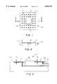
- FIG. 1is a top view of an integrated circuit package which will be processed, as shown in the subsequent figures, in accordance with the present invention.
- FIG. 2is a sectional view of the FIG. 1 integrated circuit package which is taken along the section line 2--2 in FIG. 1.
- FIG. 3is a greatly enlarged view of a portion of the FIG. 2 section which encompasses two I/O pads.
- FIG. 4shows a stencil which is used to hold solder flux for the I/O pads of the FIG. 1 integrated circuit package.
- FIG. 5shows a step in which the FIG. 4 stencil is filled with solder flux.
- FIG. 6shows a step in which the pins of a pin block are dipped into the solder flux in the stencil of FIG. 5.
- FIG. 7shows a step in which the flux coated pins of the pin block are removed from the stencil of FIG. 6.
- FIG. 8shows a step in which the flux coated pins in the pin block of FIG. 7 are touched against the I/O pads in the integrated circuit package of FIG. 1.
- FIG. 9is an enlarged sectional view, similar to FIG. 3, of the integrated circuit package which shows the solder flux that is dispensed on the I/O pads by the steps of FIGS. 5-8.
- FIG. 10shows a prior art integrated circuit package which contains no obstruction to the I/O pads and which is covered by a planer mask through which solder flux is pushed onto the I/O pads.
- FIG. 11shows that the planer mask of FIG. 10 will not work on the integrated circuit package of FIG. 1 because a lid obstructs the I/O pads.
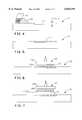
- FIG. 12shows an apparatus which places respective solder balls on each of the flux covered I/O pads on the integrated circuit package of FIG. 9.
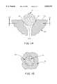
- FIG. 13shows a step in which a template, that is included within the apparatus of FIG. 12, is vibrated to thereby seat multiple solder balls which are held in respective holes in the template.
- FIG. 14is a greatly enlarged sectional view that is taken vertically through a single solder ball as it is held in an opening in the template of FIG. 13.
- FIG. 15is a horizontal sectional view, that is taken along lines 15--15 in FIG. 14, which shows how a vacuum leak past the solder balls on the template is greatly reduced by the vibrating step of FIG. 13.
- FIG. 16shows a step in which the template of FIG. 13 is turned over to thereby remove excess solder balls from the template.
- FIG. 17shows a step in which the solder balls in the template holes are placed into alignment with the I/O pads on the integrated circuit package of FIG. 1.
- FIG. 18shows a step in which the solder balls are released from the template and set onto the I/O pads of the integrated circuit package of FIG. 1.
- reference numeral 10identifies an integrated circuit package which is to be processed by the present invention.
- the integrated circuit package 10includes an integrated circuit chip 11 which lies in a cavity in the body of the package, and that cavity is covered by a lid 12.
- the bodyis comprised of laminated ceramic layers; and the lid 11 is metal.
- I/O pads (input/output pads) 13lie on a surface 10a of the integrated circuit package 10 and surround the lid 12. Each I/O pad 13 is connected by a respective microscopic conductor in the package body to a corresponding I/O terminal on the integrated circuit chip 11. Due to their small size, these conductors are not shown in FIGS. 1 and 2, but two of these conductors are shown in FIG. 3 as item 14.
- each I/O pad 13is 0.025 inches; the I/O pads have a center-to-center spacing of 0.050 inches; and the total number of I/O pads 13 is 524.
- the I/O pads 13 as drawn in FIGS. 1 and 2are greatly reduced in total number and increased in size in order to simplify those drawings.
- each of the I/O pads 13is formed in a respective recess on surface 10a of the integrated circuit package 10.
- the solder balls which will subsequently be placed on the I/O pads 13are prevented from rolling into each other. If any two solder balls are able to roll into each other, then the integrated circuit chip 11 will not operate properly because two I/O terminals on the chip 11 will be shorted together.
- each of the I/O pads 13is recessed from surface 10a of the integrated circuit package 10 by a depth D 1 which is at least 1/20th of the diameter of the solder balls that are to be placed on the I/O pads.
- the solder ballshad a diameter of 0.030 inches; and the I/O pads 13 were recessed 0.003 inches.
- a stencil 20is provided which has an indentation 21 that is wide enough to encompass all of the I/O pads 13 of the integrated circuit package 10 and which has a uniform depth D 2 .
- the indentation 21 in the stencil 20is completely filled with solder flux 22. This is achieved by using the squeegee 23 in FIG. 4 to push the mound of the solder flux 22 into the indentation 21 and remove the excess.
- a pin block 24is provided that has a base 24a from which multiple pins 24b project parallel to each other. These pins 24b have flat ends that match the pattern of the I/O pads 13 on the integrated circuit package 10; and those ends are set down in the indentation 21 of the stencil 20 which is filled with the solder flux 22.
- the ends of the pins of the pin block 24are moved into the recesses of the integrated circuit package 10 and temporarily touched against the I/O pads 13. This step transfers a portion of the solder flux from the ends of the pins on the pin block 24 onto the I/O pads 13. This is illustrated in FIG. 9 wherein the solder flux which is transferred to the I/O pads 13 is indicated by reference numeral 22.
- a critical result which is achievedis that the lid 12, which projects above the I/O pads 13, does not interfere with the solder dispensing process. This result occurs because the pins 24b on the pin block 24 are long enough to hold the base 24a of the pin block above the lid 12 when the ends of pins touch the I/O pads 13.
- the amount of solder flux 22 which is transferred to the I/O pads 13only partially fills the recesses in which the I/O pads lie by between 20% and 80%.
- the riskincreases that some flux will be pushed out of the recesses when the solder balls are placed on the I/O pads, and this in turn can short two I/O pads together when the solder balls are subsequently melted and resolidified.
- the amount of flux in the recessesis too small, then the solder balls will not properly fuse to the I/O pads 13, and thus an open circuit can occur.
- the recesses in which the I/O pads liecan be accurately filled part way with the solder flux 22. This accuracy is achieved by properly selecting the depth D 2 of the solder flux in the template 20 and its viscosity.
- the solder flux 22has a viscosity at room temperature of about 250-350 poise, which is similar to the viscosity of Vaseline.
- the flux 20 which is transferred to the ends of the pins 24b by the step of FIG. 7is about one-third as thick as the depth D 2 of the solder flux in the stencil 20; and, by the step of FIG. 8, about one-third of the solder flux on the ends of the pins 24b is transferred to the I/O pads 13.
- the depth D 2 of the solder flux in template 20should be selected such that (1/3)(1/3)D 2 is less than 80% D 1 and is more than 20% D 1 . This is achieved by confining D 2 to be four to six times larger than the depth D 1 of the recessed I/O pads. In the above-described actual embodiment where D 1 is 0.003 inches, the depth D 2 was set at 0.015 inches.
- solder fluxhas been dispensed on the I/O pads by squeezing the solder flux with a squeegee through respective holes in a planar mask which lies flat on the component and exposes only the I/O pads. This is illustrated in FIG. 10 wherein the component is identified by reference numeral 10' and the mask is identified by reference numeral 30.
- FIG. 11shows that due to the obstruction which the lid 12 presents, a gap 31 exists between the mask 30 and the component surface 10a.
- a squeegeeis used to squeeze the solder flux 22 through the holes in the mask 30 of FIG. 11, that flux 22 will fill the gap 31 and bridge two or more adjacent I/O pads 13. Those I/O pads will subsequently become shorted together when solder balls are placed on them, melted, and resolidified. Also, the squeegee will bend and crease the mask 30 in FIG. 11 around the lid 12, and thus the mask 30 will not be reusable.
- the I/O pads 13lie in recesses which are to be filled only part way with the solder flux 22.
- the recesseswill be overfilled. This is because the flux 22 which is pushed through each hole in the mask 30 will fill the recess and will also fill each hole in the mask.
- solder ballsare placed on the flux covered I/O pads by the steps of FIGS. 12-18.
- reference numeral 40identifies an apparatus by which the steps of FIGS. 12-18 are carried out.
- a flat base 41which extends perpendicular to the base
- an arm 43which pivots on the post at point 42a
- a template 44which pivots on the arm at point 43a
- a position control mechanism 45which moves a plate 46, a stop 47 for the arm 43
- a camera 48which is coupled to a visual display 49.
- the integrated circuit package 10, with its flux coated I/O pads 13,is placed on the plate 46 where it is held in place by a vacuum which is applied to a vacuum channel 46a. Then, by using the X, Y, and ⁇ control knobs on the position control mechanism 45, the plate 46 is moved left or right, forward or backward, and rotated in the horizontal plane. This positions the I/O pads 13 on the integrated circuit package 10 in alignment with cross hairs 49a on the visual display 49 as shown in FIG. 12.
- each opening 44bis funnel shaped and tapered from a diameter that is larger than a solder ball 51 to a diameter that is smaller than the solder ball.
- solder balls 51are poured from a container 52 onto the template face 44a; and a respective solder ball rolls into each of the openings 44b. At the same time, some excess solder balls roll off the template where they are caught in a tray 53; and some excess solder balls get trapped between the solder balls that fall into the template openings as is indicated by reference numeral 54.
- the template 44is vibrated by placing an electromechanical vibrator 55 against the template.
- This vibrator 55is model 11-11z by Ideal Industries, Inc.
- the template 44is vibrated for a time period of about five to fifteen seconds.
- solder balls 51which are held in the template openings 44b become seated in those openings. That is, the solder balls 51 jostle around in the openings 44b and settle in a position where leaks between the surface of the solder balls 51 and the side walls of the template openings 44b become minimized. This is illustrated in FIGS. 14 and 15.
- FIGS. 14 and 15a single solder ball 51 and a single template opening 44b in which the solder ball lies are magnified many times. At this level of magnification, it can be seen that the surface of the solder ball 51 is irregular and out of round. Similarly, at this level of magnification, it can be seen that the side walls of the template opening 44b are rough and. irregular.
- All of the openings 44b in the template 44are connected by a channel 44c to which a vacuum is applied after the above-described vibrating step.
- the vacuumcan be applied to the channel 44c while the vibrating step is performed and continue to be applied after the vibrating step is completed.
- the template 44is rotated 180° about point 43a on the arm 43 as shown in FIG. 16. During this step, all of the excess solder balls 51 fall off of the template 44, and the only solder balls which remain in the template are those which are held in the openings 44b by the vacuum that is applied to channel 44c.
- the vibrating step of FIG. 13is critical to the success of the process. If the template 44 is not vibrated, the vacuum leaks past the solder balls in the opening 44b will be so large that all of the solder balls drop out of the openings.
- the template face 44ais again placed in an upward position by rotating the template 44 180° about point 43a on the arm 43; and then, the arm 43 is pivoted. 180° in a counter clockwise direction about point 42a on the post 42.
- This stepis shown in FIG. 17.
- the solder balls 51 in the template 44are aligned directly with and placed on the I/O pads 13 of the integrated circuit package 10.
- solder balls 51 and the I/O pads 13are aligned as shown in FIG. 17, the vacuum is removed from the template channel 44c. Consequently, the solder balls 51 are released from the template 44 and are held only by the I/O pads 13 of the integrated circuit package 10. These solder balls are prevented from rolling on surface 10a off the I/O pads by the recesses in which the I/Os pad lie. Then the arm 43 is rotated clockwise 180° and rested against the stop 47 as shown in FIG. 18.
- the integrated circuit package 10is carefully lifted off the moveable plate 46, such that the solder balls 51 stay on the I/O pads 13, and placed in the belt furnace. There, the solder balls 51 are melted and resolidified which permanently attaches them to the I/O pads 13.
- the I/O pads 13can be arranged in any pattern on the integrated circuit package 10.
- the recesses in which those I/O pads 13 liecan be any size.
- package 10has at least two-hundred I/O pads 13; and preferably the recesses are 0.5 mils to 5.0 mils (12.7 ⁇ m to 127 ⁇ m) deep and 5 mils to 50 mils (127 ⁇ m to 1270 ⁇ m) wide.
- the integrated circuit package 10can have a different type of obstruction, other than the lid 12, which prevents a planar mask from lying flat on the surface 10a.
- the pin block 24can still be used to bypass the obstruction and dispense the solder flux on the I/O pads; and the template 44 can also still be used to place solder balls on the flux covered I/O pads.
- the body of the integrated circuit package 10can be made with epoxy glass such as FR4 material.
- an obstruction for the I/O pads 13can be formed by filling the cavity in which the integrated circuit chip 11 lies with a mound of epoxy which rises above the surface 10a.
- the pin block 24can be used to dispense the solder flux on the I/O pads even when the integrated circuit package contains no obstruction to the I/O pads. Similarly, the pin block 24 can be used to dispense the solder flux on the I/O pads 13 even when the I/O pads lie flush on the surface 10a and not in respective recesses.
- solder balls 51 which are placed on the I/O pads 13can be any desired size. But, a practical range for the solder balls is 5 mils to 50 mils (127 to 1270 ⁇ m) in diameter.
- the openings 44b in the template 44can have a variety of cross-sectional shapes.
- those openingsare funnel shaped and have side walls which are sloped 30° to 60° with respect to the horizontal plane. As the slope gets past 60°, the balls tend to stick in the template.
- the vibrating step of FIG. 13can be performed by many different types of vibrators.
- the vibratorcan be of a type which vibrates at just a single frequency such as 60 Hz; or the vibrator can be more complex and vibrate at multiple frequencies that are selectable or randomly generated.
Landscapes
- Engineering & Computer Science (AREA)
- Manufacturing & Machinery (AREA)
- Microelectronics & Electronic Packaging (AREA)
- Ceramic Engineering (AREA)
- Physics & Mathematics (AREA)
- Condensed Matter Physics & Semiconductors (AREA)
- General Physics & Mathematics (AREA)
- Computer Hardware Design (AREA)
- Power Engineering (AREA)
- Electric Connection Of Electric Components To Printed Circuits (AREA)
Abstract
Description
Claims (14)
Priority Applications (4)
| Application Number | Priority Date | Filing Date | Title |
|---|---|---|---|
| US08/789,217US5839191A (en) | 1997-01-24 | 1997-01-24 | Vibrating template method of placing solder balls on the I/O pads of an integrated circuit package |
| EP98904675AEP0958603A1 (en) | 1997-01-24 | 1998-01-22 | Vibrating template method of placing solder balls on the i/o pads of an integrated circuit package |
| JP53218198AJP3276374B2 (en) | 1997-01-24 | 1998-01-22 | Vibrating template method for placing solder balls on I/O pads of an integrated circuit package - Patents.com |
| PCT/US1998/001404WO1998033210A1 (en) | 1997-01-24 | 1998-01-22 | Vibrating template method of placing solder balls on the i/o pads of an integrated circuit package |
Applications Claiming Priority (1)
| Application Number | Priority Date | Filing Date | Title |
|---|---|---|---|
| US08/789,217US5839191A (en) | 1997-01-24 | 1997-01-24 | Vibrating template method of placing solder balls on the I/O pads of an integrated circuit package |
Publications (1)
| Publication Number | Publication Date |
|---|---|
| US5839191Atrue US5839191A (en) | 1998-11-24 |
Family
ID=25146947
Family Applications (1)
| Application Number | Title | Priority Date | Filing Date |
|---|---|---|---|
| US08/789,217Expired - LifetimeUS5839191A (en) | 1997-01-24 | 1997-01-24 | Vibrating template method of placing solder balls on the I/O pads of an integrated circuit package |
Country Status (4)
| Country | Link |
|---|---|
| US (1) | US5839191A (en) |
| EP (1) | EP0958603A1 (en) |
| JP (1) | JP3276374B2 (en) |
| WO (1) | WO1998033210A1 (en) |
Cited By (58)
| Publication number | Priority date | Publication date | Assignee | Title |
|---|---|---|---|---|
| US5985694A (en)* | 1997-09-29 | 1999-11-16 | Motorola, Inc. | Semiconductor die bumping method utilizing vacuum stencil |
| US6237219B1 (en)* | 1998-03-05 | 2001-05-29 | Matsushita Electric Industrial Co., Ltd. | Method of mounting conductive ball |
| US6247640B1 (en)* | 1996-09-14 | 2001-06-19 | Ricoh Company, Ltd. | Conductive particle arranging device and conductive particle transferring method using the same |
| US6253985B1 (en)* | 1998-12-25 | 2001-07-03 | Shibuya Kogyo Co., Ltd. | Unit for supplying solder balls |
| US6276598B1 (en)* | 1999-07-13 | 2001-08-21 | Asm Assembly Automation Ltd. | Method and apparatus for ball placement |
| WO2002007208A1 (en)* | 2000-07-18 | 2002-01-24 | Atmel Grenoble S.A. | Method for making an integrated circuit capable of being surface-mounted and resulting circuit |
| US6564991B1 (en)* | 1999-08-04 | 2003-05-20 | Shibuya Kogyo Co., Ltd. | Ball mount apparatus and mount method |
| US6607118B2 (en) | 2001-04-30 | 2003-08-19 | Asm Assembly Automation Limited | Apparatus and method for ball release |
| US20030164395A1 (en)* | 2002-03-01 | 2003-09-04 | Ho-Ming Tong | Solder ball attaching process |
| US6739498B2 (en)* | 2001-05-17 | 2004-05-25 | Intel Corporation | Solder ball attachment system |
| US20040124230A1 (en)* | 1999-07-24 | 2004-07-01 | Hertz Allen David | Application of acoustic and vibrational energy for fabricating bumped IC die and assembly of PCA's |
| US6883698B1 (en)* | 2002-08-16 | 2005-04-26 | High Tech Computer Corp. | Planting device for planting solder balls onto a chip |
| US20050274770A1 (en)* | 2004-06-07 | 2005-12-15 | Henderson Marvin A Sr | Method for the precise and reliable placement of solid metallic and non-metallic particles |
| US7045388B2 (en)* | 1996-08-27 | 2006-05-16 | Nippon Steel Corporation | Semiconductor device provided with low melting point metal bumps |
| CN1312735C (en)* | 2003-08-14 | 2007-04-25 | 宏达国际电子股份有限公司 | Ball attaching device used to attach multiple solder balls to a chip |
| US20090250506A1 (en)* | 2008-02-28 | 2009-10-08 | General Dynamics Advanced Information Systems | Apparatus and methods of attaching hybrid vlsi chips to printed wiring boards |
| US8813350B2 (en) | 2011-06-03 | 2014-08-26 | Seagate Technology Llc | Solder ball pattern forming |
| US9095074B2 (en) | 2012-12-20 | 2015-07-28 | Invensas Corporation | Structure for microelectronic packaging with bond elements to encapsulation surface |
| US9093435B2 (en) | 2011-05-03 | 2015-07-28 | Tessera, Inc. | Package-on-package assembly with wire bonds to encapsulation surface |
| US9123664B2 (en) | 2010-07-19 | 2015-09-01 | Tessera, Inc. | Stackable molded microelectronic packages |
| US9153562B2 (en) | 2004-11-03 | 2015-10-06 | Tessera, Inc. | Stacked packaging improvements |
| US9218988B2 (en) | 2005-12-23 | 2015-12-22 | Tessera, Inc. | Microelectronic packages and methods therefor |
| US9224717B2 (en) | 2011-05-03 | 2015-12-29 | Tessera, Inc. | Package-on-package assembly with wire bonds to encapsulation surface |
| US9252122B2 (en) | 2011-10-17 | 2016-02-02 | Invensas Corporation | Package-on-package assembly with wire bond vias |
| US9324681B2 (en) | 2010-12-13 | 2016-04-26 | Tessera, Inc. | Pin attachment |
| US9391008B2 (en) | 2012-07-31 | 2016-07-12 | Invensas Corporation | Reconstituted wafer-level package DRAM |
| US9412714B2 (en) | 2014-05-30 | 2016-08-09 | Invensas Corporation | Wire bond support structure and microelectronic package including wire bonds therefrom |
| US9502390B2 (en) | 2012-08-03 | 2016-11-22 | Invensas Corporation | BVA interposer |
| US9553076B2 (en) | 2010-07-19 | 2017-01-24 | Tessera, Inc. | Stackable molded microelectronic packages with area array unit connectors |
| US9583411B2 (en) | 2014-01-17 | 2017-02-28 | Invensas Corporation | Fine pitch BVA using reconstituted wafer with area array accessible for testing |
| US9601454B2 (en) | 2013-02-01 | 2017-03-21 | Invensas Corporation | Method of forming a component having wire bonds and a stiffening layer |
| US9646917B2 (en) | 2014-05-29 | 2017-05-09 | Invensas Corporation | Low CTE component with wire bond interconnects |
| US9659848B1 (en) | 2015-11-18 | 2017-05-23 | Invensas Corporation | Stiffened wires for offset BVA |
| US9685365B2 (en) | 2013-08-08 | 2017-06-20 | Invensas Corporation | Method of forming a wire bond having a free end |
| US9691679B2 (en) | 2012-02-24 | 2017-06-27 | Invensas Corporation | Method for package-on-package assembly with wire bonds to encapsulation surface |
| US9728527B2 (en) | 2013-11-22 | 2017-08-08 | Invensas Corporation | Multiple bond via arrays of different wire heights on a same substrate |
| US9735084B2 (en) | 2014-12-11 | 2017-08-15 | Invensas Corporation | Bond via array for thermal conductivity |
| US9761554B2 (en) | 2015-05-07 | 2017-09-12 | Invensas Corporation | Ball bonding metal wire bond wires to metal pads |
| US9812402B2 (en) | 2015-10-12 | 2017-11-07 | Invensas Corporation | Wire bond wires for interference shielding |
| US9842745B2 (en) | 2012-02-17 | 2017-12-12 | Invensas Corporation | Heat spreading substrate with embedded interconnects |
| US9852969B2 (en) | 2013-11-22 | 2017-12-26 | Invensas Corporation | Die stacks with one or more bond via arrays of wire bond wires and with one or more arrays of bump interconnects |
| US9888579B2 (en) | 2015-03-05 | 2018-02-06 | Invensas Corporation | Pressing of wire bond wire tips to provide bent-over tips |
| US9911718B2 (en) | 2015-11-17 | 2018-03-06 | Invensas Corporation | ‘RDL-First’ packaged microelectronic device for a package-on-package device |
| US9935075B2 (en) | 2016-07-29 | 2018-04-03 | Invensas Corporation | Wire bonding method and apparatus for electromagnetic interference shielding |
| US9953914B2 (en) | 2012-05-22 | 2018-04-24 | Invensas Corporation | Substrate-less stackable package with wire-bond interconnect |
| US9984992B2 (en) | 2015-12-30 | 2018-05-29 | Invensas Corporation | Embedded wire bond wires for vertical integration with separate surface mount and wire bond mounting surfaces |
| US10008469B2 (en) | 2015-04-30 | 2018-06-26 | Invensas Corporation | Wafer-level packaging using wire bond wires in place of a redistribution layer |
| US10008477B2 (en) | 2013-09-16 | 2018-06-26 | Invensas Corporation | Microelectronic element with bond elements to encapsulation surface |
| US10026717B2 (en) | 2013-11-22 | 2018-07-17 | Invensas Corporation | Multiple bond via arrays of different wire heights on a same substrate |
| US20190012421A1 (en)* | 2015-07-26 | 2019-01-10 | Vayo (Shanghai) Technology Co., Ltd. | Pcb stencil manufacturing method and system |
| US10181457B2 (en) | 2015-10-26 | 2019-01-15 | Invensas Corporation | Microelectronic package for wafer-level chip scale packaging with fan-out |
| US10299368B2 (en) | 2016-12-21 | 2019-05-21 | Invensas Corporation | Surface integrated waveguides and circuit structures therefor |
| US10332854B2 (en) | 2015-10-23 | 2019-06-25 | Invensas Corporation | Anchoring structure of fine pitch bva |
| US10381326B2 (en) | 2014-05-28 | 2019-08-13 | Invensas Corporation | Structure and method for integrated circuits packaging with increased density |
| US10460958B2 (en) | 2013-08-07 | 2019-10-29 | Invensas Corporation | Method of manufacturing embedded packaging with preformed vias |
| US10490528B2 (en) | 2015-10-12 | 2019-11-26 | Invensas Corporation | Embedded wire bond wires |
| CN111162024A (en)* | 2018-11-07 | 2020-05-15 | 普罗科技有限公司 | Apparatus for mounting conductive balls |
| US10804240B2 (en)* | 2018-11-07 | 2020-10-13 | Protec Co., Ltd. | Method of mounting conductive ball |
Families Citing this family (1)
| Publication number | Priority date | Publication date | Assignee | Title |
|---|---|---|---|---|
| CN110578298A (en)* | 2019-09-19 | 2019-12-17 | 常州市市政建设工程有限公司 | Concrete pouring process for top of viaduct upright post |
Citations (6)
| Publication number | Priority date | Publication date | Assignee | Title |
|---|---|---|---|---|
| US4871110A (en)* | 1987-09-14 | 1989-10-03 | Hitachi, Ltd. | Method and apparatus for aligning solder balls |
| US5088639A (en)* | 1991-01-25 | 1992-02-18 | Motorola, Inc. | Soldering process |
| US5118027A (en)* | 1991-04-24 | 1992-06-02 | International Business Machines Corporation | Method of aligning and mounting solder balls to a substrate |
| US5626277A (en)* | 1994-08-19 | 1997-05-06 | Sony Corporation | Mounting apparatus of solder-balls |
| US5655704A (en)* | 1994-08-30 | 1997-08-12 | Matsushita Electric Industrial Co., Ltd. | Method and apparatus for mounting soldering balls onto electrodes of a substrate or a comparable electronic component |
| US5680984A (en)* | 1994-05-13 | 1997-10-28 | Matsushita Electric Industrial Co., Ltd. | Apparatus and method for mounting soldering balls onto surfaces of electronic components |
Family Cites Families (10)
| Publication number | Priority date | Publication date | Assignee | Title |
|---|---|---|---|---|
| US5164336A (en)* | 1989-09-11 | 1992-11-17 | Nippon Steel Corporation | Method of connecting tab tape to semiconductor chip, and bump sheet and bumped tape used in the method |
| US5279045A (en)* | 1990-01-31 | 1994-01-18 | Hitachi, Ltd. | Minute particle loading method and apparatus |
| US5205896A (en)* | 1992-02-03 | 1993-04-27 | Hughes Aircraft Company | Component and solder preform placement device and method of placement |
| US5284287A (en)* | 1992-08-31 | 1994-02-08 | Motorola, Inc. | Method for attaching conductive balls to a substrate |
| JPH06310515A (en)* | 1993-04-22 | 1994-11-04 | Hitachi Ltd | Fine sphere alignment mounting method |
| US5431332A (en)* | 1994-02-07 | 1995-07-11 | Motorola, Inc. | Method and apparatus for solder sphere placement using an air knife |
| JP3152077B2 (en)* | 1994-08-25 | 2001-04-03 | 松下電器産業株式会社 | Solder ball transfer device and solder ball suction method |
| JP3211613B2 (en)* | 1994-08-25 | 2001-09-25 | 松下電器産業株式会社 | Transfer method of solder ball |
| US5657528A (en)* | 1994-08-25 | 1997-08-19 | Matsushita Electric Industrial Co., Ltd. | Method of transferring conductive balls |
| JPH0878422A (en)* | 1994-09-08 | 1996-03-22 | Hitachi Ltd | Ball-shaped external electrode formation method |
- 1997
- 1997-01-24USUS08/789,217patent/US5839191A/ennot_activeExpired - Lifetime
- 1998
- 1998-01-22WOPCT/US1998/001404patent/WO1998033210A1/enactiveSearch and Examination
- 1998-01-22JPJP53218198Apatent/JP3276374B2/ennot_activeExpired - Fee Related
- 1998-01-22EPEP98904675Apatent/EP0958603A1/ennot_activeCeased
Patent Citations (6)
| Publication number | Priority date | Publication date | Assignee | Title |
|---|---|---|---|---|
| US4871110A (en)* | 1987-09-14 | 1989-10-03 | Hitachi, Ltd. | Method and apparatus for aligning solder balls |
| US5088639A (en)* | 1991-01-25 | 1992-02-18 | Motorola, Inc. | Soldering process |
| US5118027A (en)* | 1991-04-24 | 1992-06-02 | International Business Machines Corporation | Method of aligning and mounting solder balls to a substrate |
| US5680984A (en)* | 1994-05-13 | 1997-10-28 | Matsushita Electric Industrial Co., Ltd. | Apparatus and method for mounting soldering balls onto surfaces of electronic components |
| US5626277A (en)* | 1994-08-19 | 1997-05-06 | Sony Corporation | Mounting apparatus of solder-balls |
| US5655704A (en)* | 1994-08-30 | 1997-08-12 | Matsushita Electric Industrial Co., Ltd. | Method and apparatus for mounting soldering balls onto electrodes of a substrate or a comparable electronic component |
Cited By (101)
| Publication number | Priority date | Publication date | Assignee | Title |
|---|---|---|---|---|
| US7045388B2 (en)* | 1996-08-27 | 2006-05-16 | Nippon Steel Corporation | Semiconductor device provided with low melting point metal bumps |
| US6247640B1 (en)* | 1996-09-14 | 2001-06-19 | Ricoh Company, Ltd. | Conductive particle arranging device and conductive particle transferring method using the same |
| US5985694A (en)* | 1997-09-29 | 1999-11-16 | Motorola, Inc. | Semiconductor die bumping method utilizing vacuum stencil |
| US6237219B1 (en)* | 1998-03-05 | 2001-05-29 | Matsushita Electric Industrial Co., Ltd. | Method of mounting conductive ball |
| US6253985B1 (en)* | 1998-12-25 | 2001-07-03 | Shibuya Kogyo Co., Ltd. | Unit for supplying solder balls |
| US6276598B1 (en)* | 1999-07-13 | 2001-08-21 | Asm Assembly Automation Ltd. | Method and apparatus for ball placement |
| US7293567B2 (en)* | 1999-07-24 | 2007-11-13 | Allen David Hertz | Application of acoustic and vibrational energy for fabricating bumped IC die and assembly of PCA's |
| US20040124230A1 (en)* | 1999-07-24 | 2004-07-01 | Hertz Allen David | Application of acoustic and vibrational energy for fabricating bumped IC die and assembly of PCA's |
| US6564991B1 (en)* | 1999-08-04 | 2003-05-20 | Shibuya Kogyo Co., Ltd. | Ball mount apparatus and mount method |
| WO2002007208A1 (en)* | 2000-07-18 | 2002-01-24 | Atmel Grenoble S.A. | Method for making an integrated circuit capable of being surface-mounted and resulting circuit |
| US6989591B1 (en) | 2000-07-18 | 2006-01-24 | Atmel Grenoble S.A. | Method for making an integrated circuit of the surface-mount type and resulting circuit |
| US6607118B2 (en) | 2001-04-30 | 2003-08-19 | Asm Assembly Automation Limited | Apparatus and method for ball release |
| US20040182910A1 (en)* | 2001-05-17 | 2004-09-23 | Intel Corporation | Solder ball attachment system |
| US6905059B2 (en) | 2001-05-17 | 2005-06-14 | Intel Corporation | Solder ball attachment system |
| US6739498B2 (en)* | 2001-05-17 | 2004-05-25 | Intel Corporation | Solder ball attachment system |
| US6732912B2 (en)* | 2002-03-01 | 2004-05-11 | Advanced Semiconductor Engineering, Inc. | Solder ball attaching process |
| US20030164395A1 (en)* | 2002-03-01 | 2003-09-04 | Ho-Ming Tong | Solder ball attaching process |
| US6883698B1 (en)* | 2002-08-16 | 2005-04-26 | High Tech Computer Corp. | Planting device for planting solder balls onto a chip |
| CN1312735C (en)* | 2003-08-14 | 2007-04-25 | 宏达国际电子股份有限公司 | Ball attaching device used to attach multiple solder balls to a chip |
| US20050274770A1 (en)* | 2004-06-07 | 2005-12-15 | Henderson Marvin A Sr | Method for the precise and reliable placement of solid metallic and non-metallic particles |
| US9153562B2 (en) | 2004-11-03 | 2015-10-06 | Tessera, Inc. | Stacked packaging improvements |
| US9570416B2 (en) | 2004-11-03 | 2017-02-14 | Tessera, Inc. | Stacked packaging improvements |
| US9218988B2 (en) | 2005-12-23 | 2015-12-22 | Tessera, Inc. | Microelectronic packages and methods therefor |
| US9984901B2 (en) | 2005-12-23 | 2018-05-29 | Tessera, Inc. | Method for making a microelectronic assembly having conductive elements |
| US20110157855A1 (en)* | 2008-02-28 | 2011-06-30 | General Dynamics Advanced Information Systems | Integrated circuits having lead contacts and leadless contact pads connected to a surface of a printed wiring board, and methods for connecting the same |
| US20090250506A1 (en)* | 2008-02-28 | 2009-10-08 | General Dynamics Advanced Information Systems | Apparatus and methods of attaching hybrid vlsi chips to printed wiring boards |
| US9123664B2 (en) | 2010-07-19 | 2015-09-01 | Tessera, Inc. | Stackable molded microelectronic packages |
| US9570382B2 (en) | 2010-07-19 | 2017-02-14 | Tessera, Inc. | Stackable molded microelectronic packages |
| US9553076B2 (en) | 2010-07-19 | 2017-01-24 | Tessera, Inc. | Stackable molded microelectronic packages with area array unit connectors |
| US10128216B2 (en) | 2010-07-19 | 2018-11-13 | Tessera, Inc. | Stackable molded microelectronic packages |
| US9324681B2 (en) | 2010-12-13 | 2016-04-26 | Tessera, Inc. | Pin attachment |
| US10593643B2 (en) | 2011-05-03 | 2020-03-17 | Tessera, Inc. | Package-on-package assembly with wire bonds to encapsulation surface |
| US9224717B2 (en) | 2011-05-03 | 2015-12-29 | Tessera, Inc. | Package-on-package assembly with wire bonds to encapsulation surface |
| US10062661B2 (en) | 2011-05-03 | 2018-08-28 | Tessera, Inc. | Package-on-package assembly with wire bonds to encapsulation surface |
| US11424211B2 (en) | 2011-05-03 | 2022-08-23 | Tessera Llc | Package-on-package assembly with wire bonds to encapsulation surface |
| US9093435B2 (en) | 2011-05-03 | 2015-07-28 | Tessera, Inc. | Package-on-package assembly with wire bonds to encapsulation surface |
| US9691731B2 (en) | 2011-05-03 | 2017-06-27 | Tessera, Inc. | Package-on-package assembly with wire bonds to encapsulation surface |
| US8813350B2 (en) | 2011-06-03 | 2014-08-26 | Seagate Technology Llc | Solder ball pattern forming |
| US9761558B2 (en) | 2011-10-17 | 2017-09-12 | Invensas Corporation | Package-on-package assembly with wire bond vias |
| US11735563B2 (en) | 2011-10-17 | 2023-08-22 | Invensas Llc | Package-on-package assembly with wire bond vias |
| US9252122B2 (en) | 2011-10-17 | 2016-02-02 | Invensas Corporation | Package-on-package assembly with wire bond vias |
| US11189595B2 (en) | 2011-10-17 | 2021-11-30 | Invensas Corporation | Package-on-package assembly with wire bond vias |
| US10756049B2 (en) | 2011-10-17 | 2020-08-25 | Invensas Corporation | Package-on-package assembly with wire bond vias |
| US9842745B2 (en) | 2012-02-17 | 2017-12-12 | Invensas Corporation | Heat spreading substrate with embedded interconnects |
| US9691679B2 (en) | 2012-02-24 | 2017-06-27 | Invensas Corporation | Method for package-on-package assembly with wire bonds to encapsulation surface |
| US9953914B2 (en) | 2012-05-22 | 2018-04-24 | Invensas Corporation | Substrate-less stackable package with wire-bond interconnect |
| US10170412B2 (en) | 2012-05-22 | 2019-01-01 | Invensas Corporation | Substrate-less stackable package with wire-bond interconnect |
| US10510659B2 (en) | 2012-05-22 | 2019-12-17 | Invensas Corporation | Substrate-less stackable package with wire-bond interconnect |
| US9917073B2 (en) | 2012-07-31 | 2018-03-13 | Invensas Corporation | Reconstituted wafer-level package dram with conductive interconnects formed in encapsulant at periphery of the package |
| US9391008B2 (en) | 2012-07-31 | 2016-07-12 | Invensas Corporation | Reconstituted wafer-level package DRAM |
| US9502390B2 (en) | 2012-08-03 | 2016-11-22 | Invensas Corporation | BVA interposer |
| US10297582B2 (en) | 2012-08-03 | 2019-05-21 | Invensas Corporation | BVA interposer |
| US9095074B2 (en) | 2012-12-20 | 2015-07-28 | Invensas Corporation | Structure for microelectronic packaging with bond elements to encapsulation surface |
| US9615456B2 (en) | 2012-12-20 | 2017-04-04 | Invensas Corporation | Microelectronic assembly for microelectronic packaging with bond elements to encapsulation surface |
| US9601454B2 (en) | 2013-02-01 | 2017-03-21 | Invensas Corporation | Method of forming a component having wire bonds and a stiffening layer |
| US10460958B2 (en) | 2013-08-07 | 2019-10-29 | Invensas Corporation | Method of manufacturing embedded packaging with preformed vias |
| US9685365B2 (en) | 2013-08-08 | 2017-06-20 | Invensas Corporation | Method of forming a wire bond having a free end |
| US10008477B2 (en) | 2013-09-16 | 2018-06-26 | Invensas Corporation | Microelectronic element with bond elements to encapsulation surface |
| US9728527B2 (en) | 2013-11-22 | 2017-08-08 | Invensas Corporation | Multiple bond via arrays of different wire heights on a same substrate |
| US10290613B2 (en) | 2013-11-22 | 2019-05-14 | Invensas Corporation | Multiple bond via arrays of different wire heights on a same substrate |
| US9852969B2 (en) | 2013-11-22 | 2017-12-26 | Invensas Corporation | Die stacks with one or more bond via arrays of wire bond wires and with one or more arrays of bump interconnects |
| USRE49987E1 (en) | 2013-11-22 | 2024-05-28 | Invensas Llc | Multiple plated via arrays of different wire heights on a same substrate |
| US10629567B2 (en) | 2013-11-22 | 2020-04-21 | Invensas Corporation | Multiple plated via arrays of different wire heights on same substrate |
| US10026717B2 (en) | 2013-11-22 | 2018-07-17 | Invensas Corporation | Multiple bond via arrays of different wire heights on a same substrate |
| US9837330B2 (en) | 2014-01-17 | 2017-12-05 | Invensas Corporation | Fine pitch BVA using reconstituted wafer with area array accessible for testing |
| US11990382B2 (en) | 2014-01-17 | 2024-05-21 | Adeia Semiconductor Technologies Llc | Fine pitch BVA using reconstituted wafer with area array accessible for testing |
| US11404338B2 (en) | 2014-01-17 | 2022-08-02 | Invensas Corporation | Fine pitch bva using reconstituted wafer with area array accessible for testing |
| US9583411B2 (en) | 2014-01-17 | 2017-02-28 | Invensas Corporation | Fine pitch BVA using reconstituted wafer with area array accessible for testing |
| US10529636B2 (en) | 2014-01-17 | 2020-01-07 | Invensas Corporation | Fine pitch BVA using reconstituted wafer with area array accessible for testing |
| US10381326B2 (en) | 2014-05-28 | 2019-08-13 | Invensas Corporation | Structure and method for integrated circuits packaging with increased density |
| US10475726B2 (en) | 2014-05-29 | 2019-11-12 | Invensas Corporation | Low CTE component with wire bond interconnects |
| US10032647B2 (en) | 2014-05-29 | 2018-07-24 | Invensas Corporation | Low CTE component with wire bond interconnects |
| US9646917B2 (en) | 2014-05-29 | 2017-05-09 | Invensas Corporation | Low CTE component with wire bond interconnects |
| US9947641B2 (en) | 2014-05-30 | 2018-04-17 | Invensas Corporation | Wire bond support structure and microelectronic package including wire bonds therefrom |
| US9412714B2 (en) | 2014-05-30 | 2016-08-09 | Invensas Corporation | Wire bond support structure and microelectronic package including wire bonds therefrom |
| US9735084B2 (en) | 2014-12-11 | 2017-08-15 | Invensas Corporation | Bond via array for thermal conductivity |
| US9888579B2 (en) | 2015-03-05 | 2018-02-06 | Invensas Corporation | Pressing of wire bond wire tips to provide bent-over tips |
| US10806036B2 (en) | 2015-03-05 | 2020-10-13 | Invensas Corporation | Pressing of wire bond wire tips to provide bent-over tips |
| US10008469B2 (en) | 2015-04-30 | 2018-06-26 | Invensas Corporation | Wafer-level packaging using wire bond wires in place of a redistribution layer |
| US9761554B2 (en) | 2015-05-07 | 2017-09-12 | Invensas Corporation | Ball bonding metal wire bond wires to metal pads |
| US20190012421A1 (en)* | 2015-07-26 | 2019-01-10 | Vayo (Shanghai) Technology Co., Ltd. | Pcb stencil manufacturing method and system |
| US10115678B2 (en) | 2015-10-12 | 2018-10-30 | Invensas Corporation | Wire bond wires for interference shielding |
| US10490528B2 (en) | 2015-10-12 | 2019-11-26 | Invensas Corporation | Embedded wire bond wires |
| US10559537B2 (en) | 2015-10-12 | 2020-02-11 | Invensas Corporation | Wire bond wires for interference shielding |
| US9812402B2 (en) | 2015-10-12 | 2017-11-07 | Invensas Corporation | Wire bond wires for interference shielding |
| US11462483B2 (en) | 2015-10-12 | 2022-10-04 | Invensas Llc | Wire bond wires for interference shielding |
| US10332854B2 (en) | 2015-10-23 | 2019-06-25 | Invensas Corporation | Anchoring structure of fine pitch bva |
| US10181457B2 (en) | 2015-10-26 | 2019-01-15 | Invensas Corporation | Microelectronic package for wafer-level chip scale packaging with fan-out |
| US9911718B2 (en) | 2015-11-17 | 2018-03-06 | Invensas Corporation | ‘RDL-First’ packaged microelectronic device for a package-on-package device |
| US10043779B2 (en) | 2015-11-17 | 2018-08-07 | Invensas Corporation | Packaged microelectronic device for a package-on-package device |
| US9659848B1 (en) | 2015-11-18 | 2017-05-23 | Invensas Corporation | Stiffened wires for offset BVA |
| US9984992B2 (en) | 2015-12-30 | 2018-05-29 | Invensas Corporation | Embedded wire bond wires for vertical integration with separate surface mount and wire bond mounting surfaces |
| US10325877B2 (en) | 2015-12-30 | 2019-06-18 | Invensas Corporation | Embedded wire bond wires for vertical integration with separate surface mount and wire bond mounting surfaces |
| US10824785B2 (en)* | 2016-07-26 | 2020-11-03 | Vayo (Shanghai) Technology Co., Ltd. | PCB stencil manufacturing method and system |
| US10658302B2 (en) | 2016-07-29 | 2020-05-19 | Invensas Corporation | Wire bonding method and apparatus for electromagnetic interference shielding |
| US9935075B2 (en) | 2016-07-29 | 2018-04-03 | Invensas Corporation | Wire bonding method and apparatus for electromagnetic interference shielding |
| US10299368B2 (en) | 2016-12-21 | 2019-05-21 | Invensas Corporation | Surface integrated waveguides and circuit structures therefor |
| US10804240B2 (en)* | 2018-11-07 | 2020-10-13 | Protec Co., Ltd. | Method of mounting conductive ball |
| US10804239B2 (en)* | 2018-11-07 | 2020-10-13 | Protec Co., Ltd. | Apparatus for mounting conductive ball |
| CN111162024B (en)* | 2018-11-07 | 2023-02-17 | 普罗科技有限公司 | Equipment for installing conductive balls |
| CN111162024A (en)* | 2018-11-07 | 2020-05-15 | 普罗科技有限公司 | Apparatus for mounting conductive balls |
Also Published As
| Publication number | Publication date |
|---|---|
| WO1998033210A1 (en) | 1998-07-30 |
| EP0958603A1 (en) | 1999-11-24 |
| JP2000508123A (en) | 2000-06-27 |
| JP3276374B2 (en) | 2002-04-22 |
Similar Documents
| Publication | Publication Date | Title |
|---|---|---|
| US5839191A (en) | Vibrating template method of placing solder balls on the I/O pads of an integrated circuit package | |
| US5816481A (en) | Pin block method of dispensing solder flux onto the I/O pads of an integrated circuit package | |
| US6253992B1 (en) | Solder ball placement fixtures and methods | |
| US4462534A (en) | Method of bonding connecting pins to the eyelets of conductors formed on a ceramic substrate | |
| US6268275B1 (en) | Method of locating conductive spheres utilizing screen and hopper of solder balls | |
| US5695109A (en) | Solder paste inter-layer alignment apparatus for area-array on-board rework | |
| US7216424B2 (en) | Method for fabricating electrical connections of circuit board | |
| US20020092886A1 (en) | Method and apparatus for balling and assembling ball grid array and chip scale array packages | |
| US20090217520A1 (en) | Method for forming solder lumps on printed circuit board substrate | |
| US6872650B2 (en) | Ball electrode forming method | |
| US6099935A (en) | Apparatus for providing solder interconnections to semiconductor and electronic packaging devices | |
| US6191022B1 (en) | Fine pitch solder sphere placement | |
| US20060108402A1 (en) | Solder ball formation and transfer method | |
| JP3699980B2 (en) | Solder resist, formation method thereof, and solder supply method | |
| JPH09214095A (en) | Substrate, circuit module, and method of manufacturing circuit module | |
| US5874199A (en) | Method of forming oversized solder bumps | |
| JP3186350B2 (en) | Solder bump forming method and bumped electronic component | |
| WO2004105118A1 (en) | Stencil and method for depositing material onto a substrate | |
| JP2001044231A (en) | Method of forming solder bumps and wiring board, semiconductor element, semiconductor package and manufacture thereof | |
| JPH0394973A (en) | Applicator of flux | |
| JPH05191032A (en) | Method of forming creamy solder layer and dispenser device thereof | |
| Beelen‐Hendrikx et al. | Verification of flip‐chip assembly on FR4 boards | |
| KR100384338B1 (en) | Flux Application Method for Integrated Circuit Packages | |
| JPH08148819A (en) | Mounting method of ball solders | |
| JP2530881Y2 (en) | Semiconductor device lead frame |
Legal Events
| Date | Code | Title | Description |
|---|---|---|---|
| AS | Assignment | Owner name:UNISYS CORPORATION, PENNSYLVANIA Free format text:ASSIGNMENT OF ASSIGNORS INTEREST;ASSIGNORS:ECONOMY, KENNETH WALTER;NORELL, RONALD ALLEN;BUMANN, RICHARD LEIGH;REEL/FRAME:008406/0437 Effective date:19970122 | |
| STCF | Information on status: patent grant | Free format text:PATENTED CASE | |
| FPAY | Fee payment | Year of fee payment:4 | |
| FPAY | Fee payment | Year of fee payment:8 | |
| AS | Assignment | Owner name:UNISYS CORPORATION, PENNSYLVANIA Free format text:RELEASE BY SECURED PARTY;ASSIGNOR:CITIBANK, N.A.;REEL/FRAME:023312/0044 Effective date:20090601 Owner name:UNISYS HOLDING CORPORATION, DELAWARE Free format text:RELEASE BY SECURED PARTY;ASSIGNOR:CITIBANK, N.A.;REEL/FRAME:023312/0044 Effective date:20090601 Owner name:UNISYS CORPORATION,PENNSYLVANIA Free format text:RELEASE BY SECURED PARTY;ASSIGNOR:CITIBANK, N.A.;REEL/FRAME:023312/0044 Effective date:20090601 Owner name:UNISYS HOLDING CORPORATION,DELAWARE Free format text:RELEASE BY SECURED PARTY;ASSIGNOR:CITIBANK, N.A.;REEL/FRAME:023312/0044 Effective date:20090601 | |
| AS | Assignment | Owner name:UNISYS CORPORATION, PENNSYLVANIA Free format text:RELEASE BY SECURED PARTY;ASSIGNOR:CITIBANK, N.A.;REEL/FRAME:023263/0631 Effective date:20090601 Owner name:UNISYS HOLDING CORPORATION, DELAWARE Free format text:RELEASE BY SECURED PARTY;ASSIGNOR:CITIBANK, N.A.;REEL/FRAME:023263/0631 Effective date:20090601 Owner name:UNISYS CORPORATION,PENNSYLVANIA Free format text:RELEASE BY SECURED PARTY;ASSIGNOR:CITIBANK, N.A.;REEL/FRAME:023263/0631 Effective date:20090601 Owner name:UNISYS HOLDING CORPORATION,DELAWARE Free format text:RELEASE BY SECURED PARTY;ASSIGNOR:CITIBANK, N.A.;REEL/FRAME:023263/0631 Effective date:20090601 | |
| AS | Assignment | Owner name:DEUTSCHE BANK TRUST COMPANY AMERICAS, AS COLLATERA Free format text:PATENT SECURITY AGREEMENT (PRIORITY LIEN);ASSIGNOR:UNISYS CORPORATION;REEL/FRAME:023355/0001 Effective date:20090731 | |
| AS | Assignment | Owner name:DEUTSCHE BANK TRUST COMPANY AMERICAS, AS COLLATERA Free format text:PATENT SECURITY AGREEMENT (JUNIOR LIEN);ASSIGNOR:UNISYS CORPORATION;REEL/FRAME:023364/0098 Effective date:20090731 | |
| FPAY | Fee payment | Year of fee payment:12 | |
| AS | Assignment | Owner name:GENERAL ELECTRIC CAPITAL CORPORATION, AS AGENT, IL Free format text:SECURITY AGREEMENT;ASSIGNOR:UNISYS CORPORATION;REEL/FRAME:026509/0001 Effective date:20110623 | |
| AS | Assignment | Owner name:UNISYS CORPORATION, PENNSYLVANIA Free format text:RELEASE BY SECURED PARTY;ASSIGNOR:DEUTSCHE BANK TRUST COMPANY;REEL/FRAME:030004/0619 Effective date:20121127 | |
| AS | Assignment | Owner name:UNISYS CORPORATION, PENNSYLVANIA Free format text:RELEASE BY SECURED PARTY;ASSIGNOR:DEUTSCHE BANK TRUST COMPANY AMERICAS, AS COLLATERAL TRUSTEE;REEL/FRAME:030082/0545 Effective date:20121127 | |
| AS | Assignment | Owner name:UNISYS CORPORATION, PENNSYLVANIA Free format text:RELEASE BY SECURED PARTY;ASSIGNOR:WELLS FARGO BANK, NATIONAL ASSOCIATION (SUCCESSOR TO GENERAL ELECTRIC CAPITAL CORPORATION);REEL/FRAME:044416/0358 Effective date:20171005 |