US5839188A - Method of manufacturing a printed circuit assembly - Google Patents
Method of manufacturing a printed circuit assemblyDownload PDFInfo
- Publication number
- US5839188A US5839188AUS08/583,645US58364596AUS5839188AUS 5839188 AUS5839188 AUS 5839188AUS 58364596 AUS58364596 AUS 58364596AUS 5839188 AUS5839188 AUS 5839188A
- Authority
- US
- United States
- Prior art keywords
- printed circuit
- layer
- conductive
- layers
- adhesive
- Prior art date
- Legal status (The legal status is an assumption and is not a legal conclusion. Google has not performed a legal analysis and makes no representation as to the accuracy of the status listed.)
- Expired - Fee Related
Links
Images


Classifications
- H—ELECTRICITY
- H05—ELECTRIC TECHNIQUES NOT OTHERWISE PROVIDED FOR
- H05K—PRINTED CIRCUITS; CASINGS OR CONSTRUCTIONAL DETAILS OF ELECTRIC APPARATUS; MANUFACTURE OF ASSEMBLAGES OF ELECTRICAL COMPONENTS
- H05K3/00—Apparatus or processes for manufacturing printed circuits
- H05K3/46—Manufacturing multilayer circuits
- H05K3/4611—Manufacturing multilayer circuits by laminating two or more circuit boards
- H05K3/4614—Manufacturing multilayer circuits by laminating two or more circuit boards the electrical connections between the circuit boards being made during lamination
- H05K3/462—Manufacturing multilayer circuits by laminating two or more circuit boards the electrical connections between the circuit boards being made during lamination characterized by laminating only or mainly similar double-sided circuit boards
- H—ELECTRICITY
- H05—ELECTRIC TECHNIQUES NOT OTHERWISE PROVIDED FOR
- H05K—PRINTED CIRCUITS; CASINGS OR CONSTRUCTIONAL DETAILS OF ELECTRIC APPARATUS; MANUFACTURE OF ASSEMBLAGES OF ELECTRICAL COMPONENTS
- H05K1/00—Printed circuits
- H05K1/02—Details
- H05K1/14—Structural association of two or more printed circuits
- H05K1/141—One or more single auxiliary printed circuits mounted on a main printed circuit, e.g. modules, adapters
- H—ELECTRICITY
- H01—ELECTRIC ELEMENTS
- H01L—SEMICONDUCTOR DEVICES NOT COVERED BY CLASS H10
- H01L2224/00—Indexing scheme for arrangements for connecting or disconnecting semiconductor or solid-state bodies and methods related thereto as covered by H01L24/00
- H01L2224/80—Methods for connecting semiconductor or other solid state bodies using means for bonding being attached to, or being formed on, the surface to be connected
- H01L2224/83—Methods for connecting semiconductor or other solid state bodies using means for bonding being attached to, or being formed on, the surface to be connected using a layer connector
- H01L2224/8312—Aligning
- H01L2224/83136—Aligning involving guiding structures, e.g. spacers or supporting members
- H01L2224/83138—Aligning involving guiding structures, e.g. spacers or supporting members the guiding structures being at least partially left in the finished device
- H—ELECTRICITY
- H01—ELECTRIC ELEMENTS
- H01L—SEMICONDUCTOR DEVICES NOT COVERED BY CLASS H10
- H01L2924/00—Indexing scheme for arrangements or methods for connecting or disconnecting semiconductor or solid-state bodies as covered by H01L24/00
- H01L2924/01—Chemical elements
- H01L2924/01079—Gold [Au]
- H—ELECTRICITY
- H01—ELECTRIC ELEMENTS
- H01L—SEMICONDUCTOR DEVICES NOT COVERED BY CLASS H10
- H01L2924/00—Indexing scheme for arrangements or methods for connecting or disconnecting semiconductor or solid-state bodies as covered by H01L24/00
- H01L2924/013—Alloys
- H01L2924/0132—Binary Alloys
- H01L2924/01327—Intermediate phases, i.e. intermetallics compounds
- H—ELECTRICITY
- H01—ELECTRIC ELEMENTS
- H01L—SEMICONDUCTOR DEVICES NOT COVERED BY CLASS H10
- H01L2924/00—Indexing scheme for arrangements or methods for connecting or disconnecting semiconductor or solid-state bodies as covered by H01L24/00
- H01L2924/095—Indexing scheme for arrangements or methods for connecting or disconnecting semiconductor or solid-state bodies as covered by H01L24/00 with a principal constituent of the material being a combination of two or more materials provided in the groups H01L2924/013 - H01L2924/0715
- H01L2924/097—Glass-ceramics, e.g. devitrified glass
- H01L2924/09701—Low temperature co-fired ceramic [LTCC]
- H—ELECTRICITY
- H05—ELECTRIC TECHNIQUES NOT OTHERWISE PROVIDED FOR
- H05K—PRINTED CIRCUITS; CASINGS OR CONSTRUCTIONAL DETAILS OF ELECTRIC APPARATUS; MANUFACTURE OF ASSEMBLAGES OF ELECTRICAL COMPONENTS
- H05K2201/00—Indexing scheme relating to printed circuits covered by H05K1/00
- H05K2201/01—Dielectrics
- H05K2201/0183—Dielectric layers
- H05K2201/0195—Dielectric or adhesive layers comprising a plurality of layers, e.g. in a multilayer structure
- H—ELECTRICITY
- H05—ELECTRIC TECHNIQUES NOT OTHERWISE PROVIDED FOR
- H05K—PRINTED CIRCUITS; CASINGS OR CONSTRUCTIONAL DETAILS OF ELECTRIC APPARATUS; MANUFACTURE OF ASSEMBLAGES OF ELECTRICAL COMPONENTS
- H05K2201/00—Indexing scheme relating to printed circuits covered by H05K1/00
- H05K2201/10—Details of components or other objects attached to or integrated in a printed circuit board
- H05K2201/10227—Other objects, e.g. metallic pieces
- H05K2201/10378—Interposers
- H—ELECTRICITY
- H05—ELECTRIC TECHNIQUES NOT OTHERWISE PROVIDED FOR
- H05K—PRINTED CIRCUITS; CASINGS OR CONSTRUCTIONAL DETAILS OF ELECTRIC APPARATUS; MANUFACTURE OF ASSEMBLAGES OF ELECTRICAL COMPONENTS
- H05K2201/00—Indexing scheme relating to printed circuits covered by H05K1/00
- H05K2201/10—Details of components or other objects attached to or integrated in a printed circuit board
- H05K2201/10613—Details of electrical connections of non-printed components, e.g. special leads
- H05K2201/10621—Components characterised by their electrical contacts
- H05K2201/10666—Plated through-hole for surface mounting on PCB
- H—ELECTRICITY
- H05—ELECTRIC TECHNIQUES NOT OTHERWISE PROVIDED FOR
- H05K—PRINTED CIRCUITS; CASINGS OR CONSTRUCTIONAL DETAILS OF ELECTRIC APPARATUS; MANUFACTURE OF ASSEMBLAGES OF ELECTRICAL COMPONENTS
- H05K2201/00—Indexing scheme relating to printed circuits covered by H05K1/00
- H05K2201/10—Details of components or other objects attached to or integrated in a printed circuit board
- H05K2201/10613—Details of electrical connections of non-printed components, e.g. special leads
- H05K2201/10954—Other details of electrical connections
- H05K2201/10977—Encapsulated connections
- H—ELECTRICITY
- H05—ELECTRIC TECHNIQUES NOT OTHERWISE PROVIDED FOR
- H05K—PRINTED CIRCUITS; CASINGS OR CONSTRUCTIONAL DETAILS OF ELECTRIC APPARATUS; MANUFACTURE OF ASSEMBLAGES OF ELECTRICAL COMPONENTS
- H05K2203/00—Indexing scheme relating to apparatus or processes for manufacturing printed circuits covered by H05K3/00
- H05K2203/06—Lamination
- H05K2203/063—Lamination of preperforated insulating layer
- H—ELECTRICITY
- H05—ELECTRIC TECHNIQUES NOT OTHERWISE PROVIDED FOR
- H05K—PRINTED CIRCUITS; CASINGS OR CONSTRUCTIONAL DETAILS OF ELECTRIC APPARATUS; MANUFACTURE OF ASSEMBLAGES OF ELECTRICAL COMPONENTS
- H05K2203/00—Indexing scheme relating to apparatus or processes for manufacturing printed circuits covered by H05K3/00
- H05K2203/11—Treatments characterised by their effect, e.g. heating, cooling, roughening
- H05K2203/1189—Pressing leads, bumps or a die through an insulating layer
- H—ELECTRICITY
- H05—ELECTRIC TECHNIQUES NOT OTHERWISE PROVIDED FOR
- H05K—PRINTED CIRCUITS; CASINGS OR CONSTRUCTIONAL DETAILS OF ELECTRIC APPARATUS; MANUFACTURE OF ASSEMBLAGES OF ELECTRICAL COMPONENTS
- H05K3/00—Apparatus or processes for manufacturing printed circuits
- H05K3/30—Assembling printed circuits with electric components, e.g. with resistor
- H05K3/303—Surface mounted components, e.g. affixing before soldering, aligning means, spacing means
- H05K3/305—Affixing by adhesive
- H—ELECTRICITY
- H05—ELECTRIC TECHNIQUES NOT OTHERWISE PROVIDED FOR
- H05K—PRINTED CIRCUITS; CASINGS OR CONSTRUCTIONAL DETAILS OF ELECTRIC APPARATUS; MANUFACTURE OF ASSEMBLAGES OF ELECTRICAL COMPONENTS
- H05K3/00—Apparatus or processes for manufacturing printed circuits
- H05K3/30—Assembling printed circuits with electric components, e.g. with resistor
- H05K3/32—Assembling printed circuits with electric components, e.g. with resistor electrically connecting electric components or wires to printed circuits
- H05K3/34—Assembling printed circuits with electric components, e.g. with resistor electrically connecting electric components or wires to printed circuits by soldering
- H05K3/341—Surface mounted components
- H05K3/3431—Leadless components
- H05K3/3436—Leadless components having an array of bottom contacts, e.g. pad grid array or ball grid array components
- H—ELECTRICITY
- H05—ELECTRIC TECHNIQUES NOT OTHERWISE PROVIDED FOR
- H05K—PRINTED CIRCUITS; CASINGS OR CONSTRUCTIONAL DETAILS OF ELECTRIC APPARATUS; MANUFACTURE OF ASSEMBLAGES OF ELECTRICAL COMPONENTS
- H05K3/00—Apparatus or processes for manufacturing printed circuits
- H05K3/36—Assembling printed circuits with other printed circuits
- H05K3/368—Assembling printed circuits with other printed circuits parallel to each other
- H—ELECTRICITY
- H05—ELECTRIC TECHNIQUES NOT OTHERWISE PROVIDED FOR
- H05K—PRINTED CIRCUITS; CASINGS OR CONSTRUCTIONAL DETAILS OF ELECTRIC APPARATUS; MANUFACTURE OF ASSEMBLAGES OF ELECTRICAL COMPONENTS
- H05K3/00—Apparatus or processes for manufacturing printed circuits
- H05K3/40—Forming printed elements for providing electric connections to or between printed circuits
- H05K3/4038—Through-connections; Vertical interconnect access [VIA] connections
- H05K3/4053—Through-connections; Vertical interconnect access [VIA] connections by thick-film techniques
- H05K3/4069—Through-connections; Vertical interconnect access [VIA] connections by thick-film techniques for via connections in organic insulating substrates
- H—ELECTRICITY
- H05—ELECTRIC TECHNIQUES NOT OTHERWISE PROVIDED FOR
- H05K—PRINTED CIRCUITS; CASINGS OR CONSTRUCTIONAL DETAILS OF ELECTRIC APPARATUS; MANUFACTURE OF ASSEMBLAGES OF ELECTRICAL COMPONENTS
- H05K3/00—Apparatus or processes for manufacturing printed circuits
- H05K3/46—Manufacturing multilayer circuits
- H05K3/4611—Manufacturing multilayer circuits by laminating two or more circuit boards
- H05K3/4623—Manufacturing multilayer circuits by laminating two or more circuit boards the circuit boards having internal via connections between two or more circuit layers before lamination, e.g. double-sided circuit boards
- H—ELECTRICITY
- H05—ELECTRIC TECHNIQUES NOT OTHERWISE PROVIDED FOR
- H05K—PRINTED CIRCUITS; CASINGS OR CONSTRUCTIONAL DETAILS OF ELECTRIC APPARATUS; MANUFACTURE OF ASSEMBLAGES OF ELECTRICAL COMPONENTS
- H05K3/00—Apparatus or processes for manufacturing printed circuits
- H05K3/46—Manufacturing multilayer circuits
- H05K3/4644—Manufacturing multilayer circuits by building the multilayer layer by layer, i.e. build-up multilayer circuits
- H05K3/4647—Manufacturing multilayer circuits by building the multilayer layer by layer, i.e. build-up multilayer circuits by applying an insulating layer around previously made via studs
- Y—GENERAL TAGGING OF NEW TECHNOLOGICAL DEVELOPMENTS; GENERAL TAGGING OF CROSS-SECTIONAL TECHNOLOGIES SPANNING OVER SEVERAL SECTIONS OF THE IPC; TECHNICAL SUBJECTS COVERED BY FORMER USPC CROSS-REFERENCE ART COLLECTIONS [XRACs] AND DIGESTS
- Y10—TECHNICAL SUBJECTS COVERED BY FORMER USPC
- Y10T—TECHNICAL SUBJECTS COVERED BY FORMER US CLASSIFICATION
- Y10T29/00—Metal working
- Y10T29/49—Method of mechanical manufacture
- Y10T29/49002—Electrical device making
- Y10T29/49117—Conductor or circuit manufacturing
- Y10T29/49124—On flat or curved insulated base, e.g., printed circuit, etc.
- Y10T29/49126—Assembling bases
Definitions
- the inventionrelates to printed circuit assemblies and methods of manufacture therefor. More particularly, the invention relates to printed circuit assemblies and methods of manufacture thereof having controlled separations between conductive layers, and to printed circuit assemblies and methods of manufacture thereof in which multiple overlapping conductive layers are electrically interconnected.
- conductive through holesmay be drilled and plated through multiple layers to form interlayer connections.
- drilled through holesoccupy significant space on a printed circuit board, both because the through holes are formed through the entire board, regardless of which layers need be interconnected, and because most mechanical drilling processes are typically limited to holes with about 100 micron minimum diameters.
- Anisotropic adhesivesare another alternative for forming interlayer connections; however, some anisotropic adhesives do not form pure metallurgical joints, and thus may suffer from a reliability standpoint. Further, they often require coverlayers to insulate non-connected but overlapping conductive areas, thus increasing overall assembly thicknesses.
- Propagation delaysare affected by interconnecting circuitry such as printed circuit boards and assemblies principally as a result of the dielectric constant of the materials used in the circuitry.
- materials having low dielectric constantsare desirable to use for minimizing any propagation delays, and thereby increasing the range of obtainable signal speeds within a circuit.
- Impedanceis principally the combination of resistance, capacitance and inductance which create electric and magnetic fields in a circuit.
- the impedance of a circuitis also called the characteristic impedance, as it depends solely on the characteristics of the materials used and their spatial relationship. Factors such as the dielectric constants of circuitry materials and lengths and widths of conductive signal traces primarily affect the characteristic impedance of an electronic circuit.
- Matching the impedances of interconnecting circuitry with other electronic devices and connectorsis important for ensuring signal integrity in a circuit. This is because, at high frequencies, signals may get reflected when impedance mismatches are present in a circuit. Such mismatches distort signals, increase rise times, and otherwise generate errors in data transmission. Consequently, impedance matching is often necessary to provide maximum power transfer between the connected electronic components and systems and to prevent signal reflections from forming along the signal paths.
- impedance in a printed circuitis directly related to the separation between signal traces separated by an insulating layer, as well as to the dielectric constant of the material in the insulating layer.
- One controlled impedance designis the surface microstrip configuration, where a signal trace opposes a ground plane, with no other overlapping conductive layers.
- Anotheris the stripline configuration, where a signal trace is sandwiched between a pair of ground planes.
- Controlled impedancerequires that both the dielectric constant of the insulating layer, and the separation between the signal traces, to be carefully controlled. For many conventional double-sided printed circuit assemblies, this may not be a significant problem because insulating substrates such as polymer films and hardboards can usually be manufactured with carefully controlled thicknesses and dielectric constants.
- impedance controlis more difficult, typically because of the adhesives commonly used in the interlayer interconnection technologies that bond individual single- or double-sided boards together when forming such assemblies.
- a similar problemmay also exist for some two layer boards, e.g., those with opposing single sided boards connected through adhesives.
- planarityAnother important concern with many multilayer printed circuit assemblies is planarity. In particular, it may be important to maintain controlled thicknesses of layers, even in non-impedance critical applications, so that outer surfaces of an assembly are substantially planar. This may be important, for example, when populating an assembly with integrated circuit and other electronic devices, since connecting pads on the assembly for mounting these devices should have similar elevations to ensure reliable connections therebetween.
- lamination of such assembliesmay induce non-planarity. Further, the effects are cumulative with the number of layers, and consequently, the effects may be more pronounced in thicker multilayer assemblies.
- anisotropic adhesivetypically contains conductive particles disposed in a non-conductive adhesive.
- An anisotropic adhesivewhen layered between opposing conductive layers, is designed to conduct only across its thickness and not between different points within the layer. The anisotropic nature of the adhesive permits it to be layered throughout overlapping portions of conductive layers to both bond the layers together and electrically connect any opposing contact pads formed in the conductive layers.
- anisotropic adhesivesutilize conductive particles such as metal-coated polymeric or glass spheres, and some may further include additional non-conductive particles that prevent excess deformation of the conductive particles during lamination. Also, some of these particles are intended to be disposed in a single layer such that opposing contact pads connected by the particles are separated by a distance equal to the diameters of the particles.
- While such particlesmay control the separation between the electrically connected contact pads in some applications, they are not suitable for controlling the separation between conductive layers throughout an entire circuit assembly, particularly in areas where overlapping conductive portions in the layers are not electrically connected across the adhesive layer. Instead, in areas where overlapping pads or traces of conductive material are not electrically connected, a coverlayer is used (which also has the disadvantage of increasing the overall assembly thickness), or one or both conductive layers in the overlapping areas are somewhat recessed, such that the conductive particles are not capable of abutting both conductive layers directly. Otherwise, undesired electrical connections would be formed in those overlapping areas.
- interlayer electrical connections between opposing conductive layersgenerally take up a relatively small area of a printed circuit assembly
- the conductive particles in anisotropic adhesivesare not suitable for controlling the separation between conductive layers in most of an assembly.
- the electrical connections between the signal layer and the ground planesmay be quite sparse and widely separated, further minimizing the ability of such adhesives to effectively control layer separation throughout relatively large areas of the printed circuit assembly.
- the inventionaddresses these and other problems associated with the prior art in providing a printed circuit assembly and method of making the same which in one aspect utilizes an adhesive layer including a plurality of non-conductive "gauge particles" disposed within a non-conductive adhesive.
- an adhesive layerincluding a plurality of non-conductive "gauge particles" disposed within a non-conductive adhesive.
- individual gauge particlesare interposed or sandwiched at various points between the printed circuit layers such that the diameters of the particles control the separation between the circuit layers throughout the assembly.
- a “printed circuit layer”is any layer within a printed circuit assembly, whether conductive or non-conductive, and irrespective of its manner of deposition or placement on the assembly.
- a “printed circuit layer”may include conductive layers formed of metals or conductive polymers, flexible or rigid substrates, coverlayers, films, etc.
- a “printed circuit layer”will be substantially non-deformable, so that any gauge particles abutting the layer will not substantially deform the layer, but will instead control its relative position within the assembly.
- gauge particlesmay also de facto control the separation between other circuit layers in the assembly which do not abut the gauge particles, but which are connected in some manner to the circuit layers which do abut the particles.
- control of this separationmay be obtained consistent with the invention not only by interposing the gauge particles between the conductive layers, but also between one conductive layer and another layer to which the other conductive layer is attached (e.g., an insulating substrate), as well as between two such layers to which the conductive layers are attached (e.g., between two insulating substrates).
- Other combinationsmay also be used consistent with the invention.
- the particles in the adhesive layerare designated "gauge” particles because they determine or control the separation between opposing printed circuit layers in a manufactured assembly. Furthermore, the particles are constructed to be non-conductive, such that a particle may be oriented at practically any point between opposing printed circuit layers irrespective of the materials used in the opposing layers, and irrespective of whether an electrical connection has or is to be formed at this point.
- the inventionaddresses additional problems associated with the prior art in providing a printed circuit assembly and method of making the same which in another aspect interconnects contact pads on an overlapping pair of conductive layers through conductive posts formed on the contact pads on one layer and bonded to the contact pads on the other layer. Fusible material may be incorporated into the posts to form fused connections with the opposing contact pads.
- the postsmay project through apertures in a dielectric layer separating the conductive layers, or alternately, the posts may "pierce" through the dielectric layer during lamination, thereby eliminating a separate aperture-formation step.
- a printed circuit assemblywhich includes first and second printed circuit boards, each printed circuit board including an insulating substrate with a conductive layer disposed thereon, the conductive layer on the first printed circuit board including a first contact pad opposing a second contact pad on the conductive layer on the second printed circuit board, and at least one of the first and second printed circuit boards including a second conductive layer formed on the opposite surface of the insulating substrate; a dielectric layer disposed between the first and second printed circuit boards; and a conductive post, formed on the first contact pad, the conductive post extending across the dielectric layer and abutting the second contact pad, thereby electrically connecting the first and second contact pads.
- a method of manufacturing a printed circuit assemblyincludes the step of forming a conductive post on a first printed circuit board, the printed circuit board including an insulating substrate with a conductive layer disposed thereon, wherein the conductive post is disposed on a first contact pad disposed in the conductive layer of the first printed circuit board; placing a second printed circuit board over the first printed circuit board with a second contact pad aligned with the conductive post and with a dielectric layer disposed therebetween, the second printed circuit board including an insulating substrate with a conductive layer disposed thereon, wherein the second contact pad is disposed in the conductive layer of the second printed circuit board, and wherein at least one of the first and second printed circuit boards includes a second conductive layer formed on the opposite surface of the insulating substrate; and compressing the first and second printed circuit boards together until the conductive post extends across the dielectric layer and abuts the second contact pad, thereby electrically connecting the first and second contact pads.
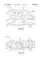
- FIG. 1is a perspective view of one preferred printed circuit assembly consistent with the principles of the invention.
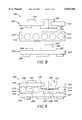
- FIG. 2is an exploded cross-sectional view of a preferred printed circuit assembly of FIG. 1.
- FIG. 3is a cross-sectional view of a preferred printed circuit assembly, taken through line 3--3 of FIG. 1.
- FIG. 4is a cross-sectional view of an alternate preferred printed circuit assembly to that of FIGS. 1-3, where gauge particles are disposed between an insulating substrate and a conductive layer.
- FIG. 5is a cross-sectional view of an alternate preferred printed circuit assembly to that of FIGS. 1-3, where gauge particles are disposed between a pair of conductive layers.
- FIG. 6is an exploded cross-section view of another alternate printed circuit assembly to that of FIGS. 1-3, where a conductive plug is formed in the adhesive layer to electrically connect opposing contact pads.
- FIG. 7is a cross-section view of the alternate printed circuit assembly of FIG. 6.
- FIG. 8is an exploded cross-section view of another alternate printed circuit assembly to that of FIGS. 1-3, where a conductive post projects through the adhesive layer to electrically connect opposing contact pads.
- FIG. 9is a cross-section view of the alternate printed circuit assembly of FIG. 8.
- FIG. 10is a cross-section view of another alternate printed circuit assembly to that of FIGS. 8-9, whereby an alternate dielectric layer is disposed between opposing printed circuit boards.
- the inventionincorporates two primary aspects.
- the firstdeals with controlling the separation between opposing printed circuit layers in a printed circuit assembly.
- the seconddeals with forming interlayer interconnections between opposing conductive layers in a printed circuit assembly. While both aspects of the invention are useful when used in conjunction with one another, it should be appreciated that neither aspect should be limited to use only in conjunction with the other.
- FIG. 1shows a preferred printed circuit assembly 10 consistent with the principles of the present invention.
- Assembly 10generally includes a pair of double-sided printed circuit boards 20, 30 joined by an adhesive layer 40.
- One principle benefit of the inventionis the ability to reliably control circuit layer separations through the use of an adhesive layer having gauge particles dispersed therein. Controlled layer separation may be beneficial for controlling impedance, as well as to ensure planarity throughout an assembly.
- preferred embodiments of the inventionoperate by interposing controlled diameter gauge particles between opposing or overlapping portions of printed circuit layers and compressing the circuit layers such that the particles abut both opposing layers and thereby define the separation therebetween.
- controlling the separation between printed circuit layersalso controls the separation between other layers connected thereto. This also has the effect of minimizing any additive planarity distortions in a multiple layer printed circuit assembly.
- the gauge particlesmay be interposed between any two opposing printed circuit layers, which as discussed above may include numerous materials, including conductive layers formed of metals or conductive polymers, flexible or rigid substrates, coverlayers, films, etc. These layers are preferably substantially non-deformable so that they will abut the particles but will not substantially deform or compress at their point of abutment with the particles, to thereby fix their relative separations in the assembly.
- printed circuit assembly 10utilizes gauge particles which are sized to abut opposing insulating substrates. With conductive layers mounted to the substrates, the separation between the conductive layers is also controlled, which may be important for impedance control, as well as form maintaining planarity throughout the assembly.
- Assembly 10generally includes a pair of printed circuit boards 20, 30 joined by an adhesive layer 40. Also shown are a plurality of through holes 12 joining the opposing conductive layers on each circuit board, as well as an integrated circuit chip 14, which is one of innumerable types of electronic devices that may be populated on assembly 10.
- printed circuit board 20includes an insulating substrate 22 with opposing conductive layers 24 and 26.
- printed circuit board 30includes an insulating substrate 32 with opposing conductive layers 34, 36.
- Insulating substrates 22, 32may be any type of flexible or rigid dielectric material suitable for use as a substrate, including polyimide, polyester, PEN, polyetherimide, epoxy, ceramic, impregnated woven or non-woven glass, among others.
- Conductive layers 24, 26, 34, 36are preferably deposited and patterned on substrates 22 and 32 in any manner generally known in the art, including various additive, semi-additive or subtractive techniques.
- Deposition of the conductive layersmay be performed via adhesiveless processes such as vacuum metallization, sputtering, ion plating, chemical vapor deposition, electroplating, electroless plating, etc., as well as through the use of adhesives.
- the conductive layersmay be formed of single metal layers or composite layers formed by different processes, and may include metals such as copper, gold, chromium, aluminum, palladium, tin, etc., as well as conductive polymers and the like.
- substrates 22, 32are formed of polyimide, and conductive layers 24, 26, 34, 36 are formed via the NOVACLAD® process, which is the subject matter of U.S. Pat. Nos. 5,112,462; 5,137,791 and 5,364,707 to Swisher, and assigned to Sheldahl, Inc.
- This processgenerally includes the steps of (1) treating the substrate with a plasma made up of ionized oxygen produced from a metallic electrode to form a metal/oxide treated film and (2) forming metallized interconnection layers on the treated film, preferably either by vacuum metallization of metal, or by combination of vacuum metallization of metal and an additional step of electroplating metal on top of the vacuum-deposited metal.
- the first step in the processproduces a bonding surface on the film which is capable of securing metal interconnection layers which, unlike adhesive-based substrates, have excellent delamination resistance, especially when exposed to heat, chemical treatment, mechanical stress or environmental stress.
- the boardthus metallized, may be etched in a conventional manner to form the desired circuit patterns in the conductive layers.
- Through holesmay be formed on printed circuit boards 20, 30 e.g., by drilling vias in the substrate prior to metallization such that conductive material is deposited thereon. It some applications the conductive material deposited on the via walls may completely fill the vias, such that no aperture remains within the through hole. Coverlayers may also be deposited over the patterned conductive layers in some applications. Other variations, e.g., drilling after plating, will be apparent to one of ordinary skill in the art.
- an adhesive layer 40is preferably interposed between boards 20, 30.
- Layer 40preferably is a dried and cured B-stage layer formed of a plurality of non-conductive gauge particles 44 interspersed in a non-conductive adhesive 42.
- the layermay be deposited on one of the printed circuit boards via screen printing, roll coating or another suitable process.
- the adhesive 42 used in layer 40is preferably a non-conductive thermosetting adhesive such as polyimide, epoxy, butyrl phenolic, etc. and combinations thereof. Other adhesives such as pressure sensitive and thermoplastic adhesives may also be used in the alternative.
- the adhesive usedshould have suitable adhesive and flow characteristics, and may also be selected based upon concerns such as dielectric constant and temperature resistance.
- the adhesive used in the preferred embodimentis a polyimide thermosetting adhesive, which has a dielectric constant of about 4.4 (measured at 1 Mhz under 4.8.3.1.4. of Mil-P-13949 Std.), and which is also high temperature resistant.
- the gauge particlesare preferably non-compactible spherical particles formed of solid or hollow non-conductive material such as glass, polymer, silica, ceramic, etc.
- the material used for the particlesmay also be selected based upon a specific dielectric strength to tailor the adhesive layer to a controlled dielectric constant.
- the overall dielectric constant of the adhesive layermay be decreased below that of the adhesive itself.
- the particlesmay also have different geometries than spherical.
- the particlesare hollow glass spheres. Using the preferred size and distribution ranges for the particles, this results in an overall dielectric constant for the adhesive layer of about 1.5 to 3 (measured at 1 Mhz under 4.8.3.1.4. of Mil-P-13949 Std.).
- the sizes of the particlesare preferably controlled to be substantially the same throughout the adhesive layer, with preferably at least 30 percent of the particles being between about +/-10 percent of a mean diameter.
- the loading or distribution of particles in the adhesiveis preferably about 30 to 75 percent by volume, although other particle densities may be required in different applications, particularly where the particles are used to define the separations between other types of printed circuit layers.
- the final separation distances, the layouts of the boards, and other considerationsmay also impact the sizes and distributions of the particles in the adhesive.
- the particlesare preferably dispersed uniformly throughout the adhesive, then the adhesive is layered, dried and cured to form a B-stage adhesive layer. The layer is then interposed between the printed circuit boards, and the entire assembly is laminated under heat and pressure to compress the boards together, as shown in FIG. 3.
- the gauge particlesare trapped between the circuit boards to abut the opposing insulating layers at areas where there are no conductive layers. In areas where one or more conductive layers are present, the particles are typically displaced to areas having no conductive layers (i.e., "exposed areas" of the insulating substrates).
- the adhesiveflows into the recesses between the boards, and any excess adhesive is squeezed out of the sides of the assembly. The extent to which the boards are compressed together during lamination is determined by the diameters of the gauge particles, as these particles abut opposing printed circuit layers to define the final layer separations for the assembly.
- the mean diameter for the population of particlesis preferably selected to provide controlled separation between printed circuit layers.
- the diameter of the particles dis preferably selected to control the connected distance x between insulating substrates 22 and 32 (best seen in FIG. 3).
- controlling the distance between these layersalso indirectly controls the distance y between the conductive layers 26, 36.
- the distance y between conductive layers across the adhesive layermay be desirable to equal the distance z between conductive layers across the insulating substrates.
- the mean diameter of the gauge particleswould need to be 80 microns to provide a 50 micron separation between conductive layers across the adhesive layer. It may also be desirable to match the dielectric constant of the adhesive layer with that of the insulating substrates.
- FIG. 4illustrates an assembly 50 having an adhesive layer 80 (having gauge particles 84 disposed in an adhesive 82) for bonding together a pair of printed circuit boards 60, 70, with insulating substrates 62, 72 and conductive layers 64, 66, 74.
- the plurality of gauge particles 84abut, on printed circuit board 60, the insulating substrate 62; and on printed circuit board 70, the conductive layer 74.
- the diameters d of the particlesare controlled to indirectly set the distance y between the conductive layers 66, 74, as well as the distance x between the insulating substrates 62, 72.
- the particlesare displaced from any areas having two layers of overlapping conductive material.
- the configuration shown in FIG. 4may be useful in applications having ground, power or shield planes where conductive material fully covers a surface of at least one printed circuit board.
- FIG. 5illustrates an assembly 100 having an adhesive layer 130 (having gauge particles 134 disposed in an adhesive 132) for bonding together a pair of printed circuit boards 110, 120, with insulating substrates 112, 122 and conductive layers 114, 116, 124.
- the diameters d of the particlesare controlled to directly set the distance y between the conductive layers 114, 124, as well as to indirectly set the distance x between the insulating substrates 112, 122.
- Any particles disposed in areas without any overlapping conductive materialtend to "float" within the adhesive and not control layer separation.
- due to the non-conductive nature of the particlesthey do not conduct across the adhesive layer and cause any potential undesired short circuits in the assembly.
- Other printed circuit layersmay abut the gauge particles, including any coverlayers formed over the conductive layers on a circuit board.
- Additional printed circuit boardsmay also be bonded together using additional adhesive layers, e.g., to produce multilayer assemblies having five or more conductive layers.
- a dielectric materialmay be "filled in” between circuit traces to provide a more planar surface for the printed circuit boards, whereby the gauge particles would abut two types of layers on the same printed circuit board.
- non-signal transmitting areasthat is, those areas where conductive material would otherwise not be used
- the conductive material in these non-signal transmitting areasmay serve no other purpose than controlling separation, or it may be used as shielding or other purposes, for example.
- particle sizesmay be used in different areas of an assembly, e.g., if a ground or shield plane is only provided in one area of an assembly, and the particles and/or adhesive may be used in only some overlapping portions of the circuit boards.
- other manners of depositing an adhesive layer and compressing the assemblymay also be used. Other modifications will be apparent to one skilled in the art.
- the preferred adhesive layersmay also include pad interconnecting means for electrically connecting any contact pads on the printed circuit boards at discrete locations across the adhesive layers. Any number of manners may be used to form conductive areas through an adhesive layer.
- printed circuit assembly 140 of FIGS. 6 and 7illustrates one manner of forming pad connections whereby an aperture 175 is formed in an adhesive layer 170 (having gauge particles 174 in an adhesive 172) and filled with conductive material 176.
- the resulting layeris interposed between a pair of printed circuit boards 150, 160 (with substrates 152, 162 and conductive layers 154, 156, 164, 166), with the conductive material 176 in layer 170 aligned with opposing pads 157 (e.g., formed at a through hole 158) and 167.
- conductive material 176preferably fuses with pads 157, 167 to form a reliable interconnection therebetween concurrent with the placement of particles 174 between substrates 152, 162.
- Apertures 175 in layer 170may be formed by drilling, punching, stamping, laser ablation, etc.
- Conductive material 176may be deposited in the apertures by a number of processes, including electroplating, screen printing, ink jet printing, etc.
- the conductive materialmay be a metal such as copper, or may be a conductive ink (cured or uncured) or a fusible material such as solder particles. Two preferred manners include screen printing a fusible conductive ink, and ink jet printing fine solder particles.
- interlayer interconnectionse.g., drilling and plating through holes after lamination
- drilling and plating through holes after laminationmay also be used without departing from the spirit and scope of the invention.
- the preferred embodiments of the inventionrealize controlled separation between printed circuit layers, be they insulating substrates, conductive layers, other layers, or combinations thereof.
- the controlled separationbenefits circuit design in controlled impedance applications, since the impedances across the adhesive layers may be reliably determined.
- the planarity of the resulting assembliesis improved, which is particularly important as the number of layers in an assembly increases since planarity errors are additive as the number of layers increases.
- Thishas the added advantage of maintaining relatively constant elevations of mounting pads on external surfaces of an assembly to which electronic devices such as integrated circuits are attached. Other modifications may be made to these preferred embodiments without departing from the spirit and scope of the invention.
- a second aspect of the inventionis directed to forming an interlayer interconnection between opposing conductive layers in a printed circuit assembly, in particular by forming conductive "posts" or similar structures on one of the printed circuit boards which are bonded with a pad on the other printed circuit board.
- This second aspect of the inventionis particularly suitable for use in conjunction with providing controlled separation using an adhesive layer in the manner disclosed herein.
- this interlayer interconnection processmay also be used across other dielectric layers, as will be set forth below.
- printed circuit assembly 180 of FIGS. 8 and 9illustrates a manner of forming interlayer pad connections whereby a first printed circuit board 200, with a pair of conductive layers 204, 206 formed on an insulating substrate 202, has a conductive post formed on a contact pad 207.
- the postis comprised of a copper layer 208 coated by a fusible material 209 such as tin.
- the copper and tinare preferably deposited by electroplating using a semi-additive process, although other processes, including subtractive and additive metal deposition processes, screen printing processes, stencil printing processes (e.g., stenciling conductive ink coupled with subsequent curing/sintering of the ink), etc. may also be used.
- Other conductive materialssuch as any number of binary and tertiary metals, fusible materials, and combinations thereof may be used for layer 208.
- a layer of dry film photoresistis applied over a copper foil printed circuit board, then the photoresist is imaged with the desired circuit pattern and developed, and copper is electroplated through the resulting mask to form the desired circuit pattern.
- a second layer of photoresistis applied over the first layer and is exposed and developed with the pattern of the conductive posts to be formed on the printed circuit.
- the postsare electroplated to thickness with copper, then capped by an electrodeposited layer of tin.
- the photoresistis stripped off and the excess copper is etched away.
- the thickness to which copper layer 208 on each post is platedis primarily dependent upon the desired connected distance between the opposing contact pads, and when used in conjunction with gauge particle-filled adhesive, is dependent upon the diameters of the particles. For example, it may be desirable to provide connected distances between pads in the range of about 1 to 4 mils (50 to 100 microns), with the thickness of copper layer 208 preferably being in a similar range.
- Tin layer 209is preferably immersion, electroless or electroplated to a thickness selected to provide sufficient material for forming a fused connection between copper layer 208 and the opposing contact pad, preferably in the range of about 8 to 50 micro inches.
- the postscan also have different profiles, e.g., circular, rectangular, etc.
- the maximum width or diameter of the postsmay be selected depending upon resistance requirements, current handling capability, and contact pad size, typically in the range of about 50 to 100 microns.
- the poststypically do not require any additional surface area on a board beyond the contact pads to which they are mounted, and they are preferably about 1/2 the diameter of the contact pads to allow for some misalignment. Accordingly, in preferred embodiments, the posts generally do not significantly impact the overall pitch (i.e., the minimum combined signal trace spacing and width) of the board.
- Printed circuit board 200is preferably interconnected via lamination to a second board 190 (with conductive layers 194, 196 formed on a substrate 192) across an adhesive layer 210 (with gauge particles 214 in an adhesive 212).
- a second board 190with conductive layers 194, 196 formed on a substrate 192
- an adhesive layer 210with gauge particles 214 in an adhesive 212
- Layer 199may be, for example, about 8 to 50 micro inches in thickness, and formed of gold or a similar material that promotes adhesion with a fusible metal such as tin layer 209.
- the adhesion promoting layermay also not be necessary in some applications.
- the post formed of layers 208, 209may "pierce" through layer 210 and contact pad 197 (shown at through hole 198) formed on board 190.
- Fusible layer 209preferably reflows and fuses to the gold layer 199 over pad 197 to form a reliable electrical interconnect with pad 207.
- the postsDue to the high unit load of the posts, they will generally displace the adhesive to permit the fusible layers to fully contact the opposing pads and form the fused connections therebetween.
- the postsalso displace the gauge particles during the lamination process as shown in FIG. 9. With further compression, the gauge particles in the adhesive layer begin to share a portion of the applied, resulting in both controlled separation and reliable interconnects in the finished assembly.
- aperturesmay be drilled or formed in adhesive layer 210 with the apertures aligned with the posts, as opposed to the posts forming their own apertures.
- the post interlayer interconnection technology disclosed hereinmay also be used to form interconnections across other dielectric layers.
- a pair of printed circuit boards 230 and 240may be interconnected across a dielectric layer 250 with a post having copper layer 244 and fusible material 246, formed on board 240, and fused to board 230.
- Dielectric layer 250preferably includes an aligned aperture 256 through which the post may project.
- dielectric layer 250may include a base dielectric film 252 coated on both sides with an adhesive 254.
- the dielectric filmmay be a prepreg composition of woven glass impregnated with adhesives.
- Other dielectric layers, such as non-woven glass and film tapes, etc., or any other form of dielectric layer suitable for bonding opposing boards to one anothermay also be used.
- dielectric layerhaving a base film or sheet with a predetermined grid or pattern of apertures at known locations.
- postsmay be located to be aligned with apertures, thereby eliminating the need to specially drill a dielectric layer.
- interconnecting postsin the manner disclosed herein provides reliable interlayer interconnects in a simple, reliable and cost effective manner.
- the postsmay be constructed with fine dimensions and spacing, thereby increasing the obtainable packaging density for a printed circuit assembly.
- the postsare capable of forming intermetallic joints, which are typically much more reliable than adhesive joints due to the metallurgical interaction of such joints.
- the postsalso have the benefit of being deposited using standard photolithographic techniques at generally the same resolution of the overall circuit patterns, and they also reduce material costs because discrete conductive interconnections may be made only at desired locations on the boards.
- the postsmay be made smaller than the contact pads to which they are connected, thereby allowing for some misalignment of the pads during lamination. Other benefits will be appreciated by one skilled in the art.
Landscapes
- Engineering & Computer Science (AREA)
- Microelectronics & Electronic Packaging (AREA)
- Manufacturing & Machinery (AREA)
- Production Of Multi-Layered Print Wiring Board (AREA)
- Combinations Of Printed Boards (AREA)
- Printing Elements For Providing Electric Connections Between Printed Circuits (AREA)
Abstract
Description
Claims (12)
Priority Applications (14)
| Application Number | Priority Date | Filing Date | Title |
|---|---|---|---|
| US08/583,645US5839188A (en) | 1996-01-05 | 1996-01-05 | Method of manufacturing a printed circuit assembly |
| IL12510197AIL125101A (en) | 1996-01-05 | 1997-01-03 | Printed circuit multilayer assembly and method of manufacture therefor |
| AU15276/97AAU1527697A (en) | 1996-01-05 | 1997-01-03 | Printed circuit multilayer assembly and method of manufacture therefor |
| PCT/US1997/000175WO1997025844A1 (en) | 1996-01-05 | 1997-01-03 | Printed circuit multilayer assembly and method of manufacture therefor |
| CA002241446ACA2241446A1 (en) | 1996-01-05 | 1997-01-03 | Printed circuit multilayer assembly and method of manufacture therefor |
| CN97192524ACN1096222C (en) | 1996-01-05 | 1997-01-03 | Printed circuit multilayer assembly and method of manufacture therefor |
| EP97901361AEP0956748A1 (en) | 1996-01-05 | 1997-01-03 | Printed circuit multilayer assembly and method of manufacture therefor |
| KR10-1998-0705135AKR100442215B1 (en) | 1996-01-05 | 1997-01-03 | Printed wiring circuit multilayer assembly and manufacturing method thereof |
| MYPI97000015AMY113149A (en) | 1996-01-05 | 1997-01-03 | Method of manufacturing a printed circuit assembly |
| BR9706961-2ABR9706961A (en) | 1996-01-05 | 1997-01-03 | Multiple layer assembly of printed circuit and manufacturing method for it |
| JP09525336AJP2000515680A (en) | 1996-01-05 | 1997-01-03 | Printed circuit multilayer assembly and method of manufacturing the same |
| TW086101152ATW342580B (en) | 1996-01-05 | 1997-01-31 | Printed circuit assembly and method of manufacture therefor |
| US09/122,241US6246014B1 (en) | 1996-01-05 | 1998-07-24 | Printed circuit assembly and method of manufacture therefor |
| US09/195,913US6147870A (en) | 1996-01-05 | 1998-11-19 | Printed circuit assembly having locally enhanced wiring density |
Applications Claiming Priority (1)
| Application Number | Priority Date | Filing Date | Title |
|---|---|---|---|
| US08/583,645US5839188A (en) | 1996-01-05 | 1996-01-05 | Method of manufacturing a printed circuit assembly |
Related Child Applications (2)
| Application Number | Title | Priority Date | Filing Date |
|---|---|---|---|
| US09/122,241DivisionUS6246014B1 (en) | 1996-01-05 | 1998-07-24 | Printed circuit assembly and method of manufacture therefor |
| US09/195,913Continuation-In-PartUS6147870A (en) | 1996-01-05 | 1998-11-19 | Printed circuit assembly having locally enhanced wiring density |
Publications (1)
| Publication Number | Publication Date |
|---|---|
| US5839188Atrue US5839188A (en) | 1998-11-24 |
Family
ID=24334001
Family Applications (2)
| Application Number | Title | Priority Date | Filing Date |
|---|---|---|---|
| US08/583,645Expired - Fee RelatedUS5839188A (en) | 1996-01-05 | 1996-01-05 | Method of manufacturing a printed circuit assembly |
| US09/122,241Expired - Fee RelatedUS6246014B1 (en) | 1996-01-05 | 1998-07-24 | Printed circuit assembly and method of manufacture therefor |
Family Applications After (1)
| Application Number | Title | Priority Date | Filing Date |
|---|---|---|---|
| US09/122,241Expired - Fee RelatedUS6246014B1 (en) | 1996-01-05 | 1998-07-24 | Printed circuit assembly and method of manufacture therefor |
Country Status (12)
| Country | Link |
|---|---|
| US (2) | US5839188A (en) |
| EP (1) | EP0956748A1 (en) |
| JP (1) | JP2000515680A (en) |
| KR (1) | KR100442215B1 (en) |
| CN (1) | CN1096222C (en) |
| AU (1) | AU1527697A (en) |
| BR (1) | BR9706961A (en) |
| CA (1) | CA2241446A1 (en) |
| IL (1) | IL125101A (en) |
| MY (1) | MY113149A (en) |
| TW (1) | TW342580B (en) |
| WO (1) | WO1997025844A1 (en) |
Cited By (31)
| Publication number | Priority date | Publication date | Assignee | Title |
|---|---|---|---|---|
| US6299749B1 (en) | 1999-10-25 | 2001-10-09 | Molex Incorporated | Method of fabricating an electrical component |
| US6315856B1 (en)* | 1998-03-19 | 2001-11-13 | Kabushiki Kaisha Toshiba | Method of mounting electronic component |
| US20020015780A1 (en)* | 2000-07-11 | 2002-02-07 | William Holm | Method and apparatus for applying viscous medium onto a substrate |
| US20020014602A1 (en)* | 2000-07-11 | 2002-02-07 | William Holm | Method and apparatus for providing a substrate with viscous medium |
| US20020088540A1 (en)* | 2001-01-08 | 2002-07-11 | Chan Albert W. | Method for joining large substrates |
| US6421248B1 (en)* | 1997-01-15 | 2002-07-16 | Infineon Technologies Ag | Chip card module |
| US20020129894A1 (en)* | 2001-01-08 | 2002-09-19 | Kuo-Chuan Liu | Method for joining and an ultra-high density interconnect |
| US6461677B1 (en) | 2000-04-18 | 2002-10-08 | Molex Incorporated | Method of fabricating an electrical component |
| US6484045B1 (en)* | 2000-02-10 | 2002-11-19 | Medtronic Minimed, Inc. | Analyte sensor and method of making the same |
| US6484299B1 (en)* | 2000-07-07 | 2002-11-19 | Micron Technology, Inc. | Method and apparatus for PCB array with compensated signal propagation |
| US6490786B2 (en)* | 2001-04-17 | 2002-12-10 | Visteon Global Technologies, Inc. | Circuit assembly and a method for making the same |
| US20030019568A1 (en)* | 2001-01-08 | 2003-01-30 | Kuo-Chuan Liu | Method for joining conductive structures and an electrical conductive article |
| US6586686B1 (en)* | 1997-06-06 | 2003-07-01 | Ibiden Co., Ltd. | Multilayer printed wiring board and method for manufacturing the same |
| US20030193786A1 (en)* | 2002-04-15 | 2003-10-16 | Ralf Greiner | Compact circuit carrier package |
| US20040020046A1 (en)* | 2001-08-09 | 2004-02-05 | Takeshi Suzuki | Production method for conductive paste and production method for printed circuit |
| US20040145249A1 (en)* | 2003-01-24 | 2004-07-29 | Brown David C. | Galvanometer motor with composite stator assembly |
| US20040203180A1 (en)* | 2000-10-17 | 2004-10-14 | Seiko Epson Corporation | Method of manufacture of active matrix substrate and liquid crystal display device |
| US20050183883A1 (en)* | 2004-02-19 | 2005-08-25 | Bois Karl J. | Printed circuit board substrate and method for constructing same |
| US20060280912A1 (en)* | 2005-06-13 | 2006-12-14 | Rong-Chang Liang | Non-random array anisotropic conductive film (ACF) and manufacturing processes |
| US20070265795A1 (en)* | 2006-05-09 | 2007-11-15 | Formfactor, Inc. | Air Bridge Structures And Methods Of Making And Using Air Bridge Structures |
| US20070296082A1 (en)* | 2006-06-23 | 2007-12-27 | Samsung Electronics Co., Ltd. | Semiconductor device having conductive adhesive layer and method of fabricating the same |
| US20080090943A1 (en)* | 2006-10-16 | 2008-04-17 | Trillion, Inc. | Epoxy compositions |
| US20080171450A1 (en)* | 2007-01-12 | 2008-07-17 | Nokia Corporation | Wafer Bump Manufacturing Using Conductive Ink |
| US20090303655A1 (en)* | 2008-06-10 | 2009-12-10 | Murata Manufacturing Co., Ltd. | Ceramic electronic component and method for manufacturing the same |
| US20100101700A1 (en)* | 2005-06-13 | 2010-04-29 | Trillion Science Inc. | Non-random array anisotropic conductive film (acf) and manufacturing processes |
| US20100263208A1 (en)* | 2007-10-30 | 2010-10-21 | Hitachi Chemical Company, Ltd. | Circuit connecting method |
| US20140048325A1 (en)* | 2011-04-29 | 2014-02-20 | Continential Automotive Gmbh | Contact surface arranged on a carrier for connecting to a counter contact surface arranged on a further carrier, and device comprising a contact surface and a counter contact surface connected thereto |
| US9102851B2 (en) | 2011-09-15 | 2015-08-11 | Trillion Science, Inc. | Microcavity carrier belt and method of manufacture |
| US20150235797A1 (en)* | 2014-02-20 | 2015-08-20 | Yazaki Corporation | Fuse |
| US9475963B2 (en) | 2011-09-15 | 2016-10-25 | Trillion Science, Inc. | Fixed array ACFs with multi-tier partially embedded particle morphology and their manufacturing processes |
| US9983448B2 (en) | 2015-07-31 | 2018-05-29 | Fujikura Ltd. | Wiring body assembly, structure with conductor layer, and touch sensor |
Families Citing this family (30)
| Publication number | Priority date | Publication date | Assignee | Title |
|---|---|---|---|---|
| US6147870A (en)* | 1996-01-05 | 2000-11-14 | Honeywell International Inc. | Printed circuit assembly having locally enhanced wiring density |
| JP3535746B2 (en)* | 1998-08-20 | 2004-06-07 | ソニーケミカル株式会社 | Flexible substrate manufacturing method |
| US6492738B2 (en) | 1999-09-02 | 2002-12-10 | Micron Technology, Inc. | Apparatus and methods of testing and assembling bumped devices using an anisotropically conductive layer |
| JP2001251061A (en)* | 2000-03-02 | 2001-09-14 | Sony Corp | Multilayer printed wiring board |
| US6477031B1 (en)* | 2000-03-22 | 2002-11-05 | Tdk Corporation | Electronic component for high frequency signals and method for fabricating the same |
| SE0004125L (en)* | 2000-11-10 | 2002-05-11 | Ericsson Telefon Ab L M | Spacer holding dielectric layer |
| JP4344101B2 (en)* | 2001-02-14 | 2009-10-14 | Okiセミコンダクタ株式会社 | Wiring structure |
| EP1296374B1 (en)* | 2001-09-14 | 2012-09-05 | STMicroelectronics Srl | Process for bonding and electrically connecting microsystems integrated in several distinct substrates |
| JP3893100B2 (en)* | 2002-10-29 | 2007-03-14 | 新光電気工業株式会社 | Electronic component mounting method on wiring board |
| KR100559937B1 (en)* | 2003-01-08 | 2006-03-13 | 엘에스전선 주식회사 | Connection method of microcircuit and connection structure by it |
| GB0302485D0 (en) | 2003-02-04 | 2003-03-05 | Plastic Logic Ltd | Pixel capacitors |
| US20040241396A1 (en)* | 2003-05-29 | 2004-12-02 | 3M Innovative Properties Company | Method of modifying a surface of a substrate and articles therefrom |
| US20040241323A1 (en)* | 2003-05-29 | 2004-12-02 | 3M Innovative Properties Company | Method for applying adhesive to a substrate |
| GB0400982D0 (en)* | 2004-01-16 | 2004-02-18 | Fujifilm Electronic Imaging | Method of forming a pattern on a substrate |
| US6989493B2 (en)* | 2004-03-03 | 2006-01-24 | Seagate Technology Llc | Electrical feedthrough assembly for a sealed housing |
| JP2006019567A (en)* | 2004-07-02 | 2006-01-19 | Seiko Epson Corp | Shielded wire |
| WO2008059695A1 (en)* | 2006-11-13 | 2008-05-22 | Konica Minolta Opto, Inc. | Lens unit, method for manufacturing lens unit, lens camera cone, method for manufacturing the lens camera cone, and image pick-up device |
| TW200941659A (en)* | 2008-03-25 | 2009-10-01 | Bridge Semiconductor Corp | Thermally enhanced package with embedded metal slug and patterned circuitry |
| JP4825286B2 (en)* | 2009-08-07 | 2011-11-30 | ナミックス株式会社 | Manufacturing method of multilayer wiring board |
| JP2011049367A (en)* | 2009-08-27 | 2011-03-10 | Panasonic Corp | Substrate connecting structure and electronic device |
| US20130000968A1 (en)* | 2011-06-30 | 2013-01-03 | Broadcom Corporation | 1-Layer Interposer Substrate With Through-Substrate Posts |
| EP2544514B1 (en)* | 2011-07-05 | 2019-03-06 | Pierburg Pump Technology GmbH | Method for testing whether a substrate is sticking to an electrically and thermally conductive body correctly |
| US9040837B2 (en)* | 2011-12-14 | 2015-05-26 | Ibiden Co., Ltd. | Wiring board and method for manufacturing the same |
| US9179547B2 (en)* | 2013-03-30 | 2015-11-03 | Shenzhen O-Film Tech Co., Ltd. | Gold finger and touch screen |
| KR101513642B1 (en)* | 2013-08-21 | 2015-04-20 | 엘지전자 주식회사 | A device of a semiconductor |
| TWI566646B (en)* | 2015-10-06 | 2017-01-11 | 挺暉工業股份有限公司 | A flexible printed circuit board, a connector assembly and an electronic device |
| CN109246925B (en)* | 2018-08-28 | 2020-03-31 | 庆鼎精密电子(淮安)有限公司 | Manufacturing method of soft and hard board |
| WO2020133421A1 (en)* | 2018-12-29 | 2020-07-02 | 深南电路股份有限公司 | Diversified assembly printed circuit board and manufacturing method |
| JP7534243B2 (en) | 2021-03-19 | 2024-08-14 | Necプラットフォームズ株式会社 | Multilayer substrate, integrated magnetic device, power supply device, and method of manufacturing multilayer substrate |
| CN115226304B (en)* | 2021-04-20 | 2025-03-21 | 庆鼎精密电子(淮安)有限公司 | Circuit board and method for manufacturing the same |
Citations (16)
| Publication number | Priority date | Publication date | Assignee | Title |
|---|---|---|---|---|
| DE2407738A1 (en)* | 1973-02-21 | 1974-08-22 | Electrovac | Connector for liq. crystal leads to circuit board - uses intermediate connector block of conductive PVC or silicon rubber |
| US3835531A (en)* | 1971-06-10 | 1974-09-17 | Int Computers Ltd | Methods of forming circuit interconnections |
| US4157932A (en)* | 1976-11-04 | 1979-06-12 | Canon Kabushiki Kaisha | Connecting method |
| EP0270067A2 (en)* | 1986-12-03 | 1988-06-08 | Sharp Kabushiki Kaisha | Method of making a semiconductor device comprising at least two semiconductor chips |
| US4814040A (en)* | 1987-04-03 | 1989-03-21 | Sharp Kabushiki Kaisha | Method of connecting electronic element to base plate |
| EP0330452A2 (en)* | 1988-02-26 | 1989-08-30 | Minnesota Mining And Manufacturing Company | Electrically conductive pressure-sensitive adhesive tape |
| EP0379736A1 (en)* | 1988-12-29 | 1990-08-01 | Japan Radio Co., Ltd | Method of manufacturing multilayered printed-wiring-board |
| US4991285A (en)* | 1989-11-17 | 1991-02-12 | Rockwell International Corporation | Method of fabricating multi-layer board |
| US5046238A (en)* | 1990-03-15 | 1991-09-10 | Rogers Corporation | Method of manufacturing a multilayer circuit board |
| JPH0548230A (en)* | 1991-08-17 | 1993-02-26 | Fuji Xerox Co Ltd | Thin-film wiring substrate |
| JPH06160880A (en)* | 1992-11-27 | 1994-06-07 | Ricoh Co Ltd | Wiring structure and method for manufacturing conductive member |
| US5318651A (en)* | 1991-11-27 | 1994-06-07 | Nec Corporation | Method of bonding circuit boards |
| US5329695A (en)* | 1992-09-01 | 1994-07-19 | Rogers Corporation | Method of manufacturing a multilayer circuit board |
| US5401913A (en)* | 1993-06-08 | 1995-03-28 | Minnesota Mining And Manufacturing Company | Electrical interconnections between adjacent circuit board layers of a multi-layer circuit board |
| US5431571A (en)* | 1993-11-22 | 1995-07-11 | W. L. Gore & Associates, Inc. | Electrical conductive polymer matrix |
| US5457881A (en)* | 1993-01-26 | 1995-10-17 | Dyconex Patente Ag | Method for the through plating of conductor foils |
Family Cites Families (59)
| Publication number | Priority date | Publication date | Assignee | Title |
|---|---|---|---|---|
| US2721822A (en) | 1953-07-22 | 1955-10-25 | Pritikin Nathan | Method for producing printed circuit |
| NL190034A (en) | 1953-08-17 | |||
| US3181986A (en) | 1961-03-31 | 1965-05-04 | Intellux Inc | Method of making inlaid circuits |
| US3350498A (en) | 1965-01-04 | 1967-10-31 | Intellux Inc | Multilayer circuit and method of making the same |
| US3475213A (en) | 1965-09-13 | 1969-10-28 | Minnesota Mining & Mfg | Electrically conductive adhesive tape |
| US3680037A (en) | 1970-11-05 | 1972-07-25 | Tech Wire Prod Inc | Electrical interconnector |
| US4174331A (en) | 1972-06-23 | 1979-11-13 | The Carborundum Company | Refractory moldable composition containing ceramic fiber and colloidal silica |
| US3823252A (en) | 1972-10-26 | 1974-07-09 | Owens Illinois Inc | Conducting element having bundled substantially parallel crystalline conductors and process for manufacture |
| US3986255A (en) | 1974-11-29 | 1976-10-19 | Itek Corporation | Process for electrically interconnecting chips with substrates employing gold alloy bumps and magnetic materials therein |
| US3982320A (en) | 1975-02-05 | 1976-09-28 | Technical Wire Products, Inc. | Method of making electrically conductive connector |
| US4050756A (en) | 1975-12-22 | 1977-09-27 | International Telephone And Telegraph Corporation | Conductive elastomer connector and method of making same |
| US4159222A (en) | 1977-01-11 | 1979-06-26 | Pactel Corporation | Method of manufacturing high density fine line printed circuitry |
| US4268849A (en)* | 1978-11-03 | 1981-05-19 | National Semiconductor Corporation | Raised bonding pad |
| JPS5668579A (en) | 1979-11-09 | 1981-06-09 | Hitachi Ltd | Connecting method by melting solder |
| US4545840A (en)* | 1983-03-08 | 1985-10-08 | Monolithic Memories, Inc. | Process for controlling thickness of die attach adhesive |
| US4667220A (en)* | 1984-04-27 | 1987-05-19 | Trilogy Computer Development Partners, Ltd. | Semiconductor chip module interconnection system |
| US4604644A (en) | 1985-01-28 | 1986-08-05 | International Business Machines Corporation | Solder interconnection structure for joining semiconductor devices to substrates that have improved fatigue life, and process for making |
| JPS6433808A (en) | 1986-10-18 | 1989-02-03 | Japan Synthetic Rubber Co Ltd | Conductive particle and conductive adhesive including it |
| KR910004797B1 (en) | 1987-04-08 | 1991-07-13 | 가시오 게이상기 가부시기가이샤 | Small electronic device and manufacturing method thereof |
| US4771159A (en) | 1987-05-27 | 1988-09-13 | Gte Government Systems Corporation | Method of soldering leadless component carriers or the like |
| US4778635A (en) | 1987-09-18 | 1988-10-18 | American Telephone And Telegraph Company | Method and apparatus for fabricating anisotropically conductive material |
| JPH01206575A (en) | 1988-02-15 | 1989-08-18 | Shin Etsu Polymer Co Ltd | Hot bond type connector with adhesive |
| US5502889A (en)* | 1988-06-10 | 1996-04-02 | Sheldahl, Inc. | Method for electrically and mechanically connecting at least two conductive layers |
| USRE35064E (en) | 1988-08-01 | 1995-10-17 | Circuit Components, Incorporated | Multilayer printed wiring board |
| US4908258A (en) | 1988-08-01 | 1990-03-13 | Rogers Corporation | High dielectric constant flexible sheet material |
| JPH0291360U (en) | 1988-12-29 | 1990-07-19 | ||
| US5235741A (en) | 1989-08-18 | 1993-08-17 | Semiconductor Energy Laboratory Co., Ltd. | Electrical connection and method for making the same |
| JPH03196650A (en) | 1989-12-26 | 1991-08-28 | Sharp Corp | Flip chip bonding |
| JPH03209734A (en) | 1990-01-11 | 1991-09-12 | Japan Radio Co Ltd | Semiconductor connection method |
| JPH03218030A (en) | 1990-01-23 | 1991-09-25 | Hitachi Ltd | Semiconductor integrated circuit device and preform bonding material used in the same |
| JP2590450B2 (en) | 1990-02-05 | 1997-03-12 | 株式会社村田製作所 | Method of forming bump electrode |
| JPH03231216A (en) | 1990-02-06 | 1991-10-15 | Nec Corp | Optical shutter |
| JP2740357B2 (en) | 1990-02-06 | 1998-04-15 | 松下電工株式会社 | Printed circuit board |
| US5538789A (en) | 1990-02-09 | 1996-07-23 | Toranaga Technologies, Inc. | Composite substrates for preparation of printed circuits |
| US5376403A (en) | 1990-02-09 | 1994-12-27 | Capote; Miguel A. | Electrically conductive compositions and methods for the preparation and use thereof |
| US5112464A (en) | 1990-06-15 | 1992-05-12 | The Dow Chemical Company | Apparatus to control reverse current flow in membrane electrolytic cells |
| US5147084A (en) | 1990-07-18 | 1992-09-15 | International Business Machines Corporation | Interconnection structure and test method |
| US5060844A (en) | 1990-07-18 | 1991-10-29 | International Business Machines Corporation | Interconnection structure and test method |
| US5137791A (en) | 1990-09-13 | 1992-08-11 | Sheldahl Inc. | Metal-film laminate resistant to delamination |
| US5112462A (en) | 1990-09-13 | 1992-05-12 | Sheldahl Inc. | Method of making metal-film laminate resistant to delamination |
| JP2906282B2 (en) | 1990-09-20 | 1999-06-14 | 富士通株式会社 | Glass-ceramic green sheet, multilayer substrate, and manufacturing method thereof |
| US5154341A (en) | 1990-12-06 | 1992-10-13 | Motorola Inc. | Noncollapsing multisolder interconnection |
| JPH04317663A (en) | 1991-04-16 | 1992-11-09 | Photonics:Kk | Stimulating device for effective spot for treatment |
| US5225966A (en) | 1991-07-24 | 1993-07-06 | At&T Bell Laboratories | Conductive adhesive film techniques |
| US5203075A (en) | 1991-08-12 | 1993-04-20 | Inernational Business Machines | Method of bonding flexible circuit to cicuitized substrate to provide electrical connection therebetween using different solders |
| US5261155A (en) | 1991-08-12 | 1993-11-16 | International Business Machines Corporation | Method for bonding flexible circuit to circuitized substrate to provide electrical connection therebetween using different solders |
| US5261593A (en) | 1992-08-19 | 1993-11-16 | Sheldahl, Inc. | Direct application of unpackaged integrated circuit to flexible printed circuit |
| US5450290A (en) | 1993-02-01 | 1995-09-12 | International Business Machines Corporation | Printed circuit board with aligned connections and method of making same |
| US5346775A (en) | 1993-02-22 | 1994-09-13 | At&T Laboratories | Article comprising solder with improved mechanical properties |
| US5324569A (en) | 1993-02-26 | 1994-06-28 | Hewlett-Packard Company | Composite transversely plastic interconnect for microchip carrier |
| US5445308A (en) | 1993-03-29 | 1995-08-29 | Nelson; Richard D. | Thermally conductive connection with matrix material and randomly dispersed filler containing liquid metal |
| US5600103A (en)* | 1993-04-16 | 1997-02-04 | Kabushiki Kaisha Toshiba | Circuit devices and fabrication method of the same |
| US5439162A (en) | 1993-06-28 | 1995-08-08 | Motorola, Inc. | Direct chip attachment structure and method |
| EP0647090B1 (en)* | 1993-09-03 | 1999-06-23 | Kabushiki Kaisha Toshiba | Printed wiring board and a method of manufacturing such printed wiring boards |
| US5346118A (en) | 1993-09-28 | 1994-09-13 | At&T Bell Laboratories | Surface mount solder assembly of leadless integrated circuit packages to substrates |
| US5492266A (en) | 1994-08-31 | 1996-02-20 | International Business Machines Corporation | Fine pitch solder deposits on printed circuit board process and product |
| US5497938A (en) | 1994-09-01 | 1996-03-12 | Intel Corporation | Tape with solder forms and methods for transferring solder to chip assemblies |
| US5468655A (en) | 1994-10-31 | 1995-11-21 | Motorola, Inc. | Method for forming a temporary attachment between a semiconductor die and a substrate using a metal paste comprising spherical modules |
| US5429293A (en) | 1994-12-19 | 1995-07-04 | Motorola, Inc. | Soldering process |
- 1996
- 1996-01-05USUS08/583,645patent/US5839188A/ennot_activeExpired - Fee Related
- 1997
- 1997-01-03CACA002241446Apatent/CA2241446A1/ennot_activeAbandoned
- 1997-01-03ILIL12510197Apatent/IL125101A/ennot_activeIP Right Cessation
- 1997-01-03MYMYPI97000015Apatent/MY113149A/enunknown
- 1997-01-03CNCN97192524Apatent/CN1096222C/ennot_activeExpired - Fee Related
- 1997-01-03AUAU15276/97Apatent/AU1527697A/ennot_activeAbandoned
- 1997-01-03KRKR10-1998-0705135Apatent/KR100442215B1/ennot_activeExpired - Fee Related
- 1997-01-03WOPCT/US1997/000175patent/WO1997025844A1/enactiveIP Right Grant
- 1997-01-03BRBR9706961-2Apatent/BR9706961A/ennot_activeApplication Discontinuation
- 1997-01-03EPEP97901361Apatent/EP0956748A1/ennot_activeCeased
- 1997-01-03JPJP09525336Apatent/JP2000515680A/ennot_activeCeased
- 1997-01-31TWTW086101152Apatent/TW342580B/enactive
- 1998
- 1998-07-24USUS09/122,241patent/US6246014B1/ennot_activeExpired - Fee Related
Patent Citations (19)
| Publication number | Priority date | Publication date | Assignee | Title |
|---|---|---|---|---|
| US3835531A (en)* | 1971-06-10 | 1974-09-17 | Int Computers Ltd | Methods of forming circuit interconnections |
| DE2407738A1 (en)* | 1973-02-21 | 1974-08-22 | Electrovac | Connector for liq. crystal leads to circuit board - uses intermediate connector block of conductive PVC or silicon rubber |
| US4157932A (en)* | 1976-11-04 | 1979-06-12 | Canon Kabushiki Kaisha | Connecting method |
| EP0270067A2 (en)* | 1986-12-03 | 1988-06-08 | Sharp Kabushiki Kaisha | Method of making a semiconductor device comprising at least two semiconductor chips |
| US4814040A (en)* | 1987-04-03 | 1989-03-21 | Sharp Kabushiki Kaisha | Method of connecting electronic element to base plate |
| EP0330452A2 (en)* | 1988-02-26 | 1989-08-30 | Minnesota Mining And Manufacturing Company | Electrically conductive pressure-sensitive adhesive tape |
| EP0607534A2 (en)* | 1988-12-29 | 1994-07-27 | Japan Radio Co., Ltd | Method of manufacturing multilayered printed-wiring-board |
| EP0379736A1 (en)* | 1988-12-29 | 1990-08-01 | Japan Radio Co., Ltd | Method of manufacturing multilayered printed-wiring-board |
| EP0607532A2 (en)* | 1988-12-29 | 1994-07-27 | Japan Radio Co., Ltd | Method of manufacturing multilayered printed-wiring-board |
| US4991285A (en)* | 1989-11-17 | 1991-02-12 | Rockwell International Corporation | Method of fabricating multi-layer board |
| US5046238A (en)* | 1990-03-15 | 1991-09-10 | Rogers Corporation | Method of manufacturing a multilayer circuit board |
| JPH0548230A (en)* | 1991-08-17 | 1993-02-26 | Fuji Xerox Co Ltd | Thin-film wiring substrate |
| US5318651A (en)* | 1991-11-27 | 1994-06-07 | Nec Corporation | Method of bonding circuit boards |
| US5545281A (en)* | 1991-11-27 | 1996-08-13 | Nec Corporation | Method of bonding circuit boards |
| US5329695A (en)* | 1992-09-01 | 1994-07-19 | Rogers Corporation | Method of manufacturing a multilayer circuit board |
| JPH06160880A (en)* | 1992-11-27 | 1994-06-07 | Ricoh Co Ltd | Wiring structure and method for manufacturing conductive member |
| US5457881A (en)* | 1993-01-26 | 1995-10-17 | Dyconex Patente Ag | Method for the through plating of conductor foils |
| US5401913A (en)* | 1993-06-08 | 1995-03-28 | Minnesota Mining And Manufacturing Company | Electrical interconnections between adjacent circuit board layers of a multi-layer circuit board |
| US5431571A (en)* | 1993-11-22 | 1995-07-11 | W. L. Gore & Associates, Inc. | Electrical conductive polymer matrix |
Cited By (57)
| Publication number | Priority date | Publication date | Assignee | Title |
|---|---|---|---|---|
| US6421248B1 (en)* | 1997-01-15 | 2002-07-16 | Infineon Technologies Ag | Chip card module |
| US6586686B1 (en)* | 1997-06-06 | 2003-07-01 | Ibiden Co., Ltd. | Multilayer printed wiring board and method for manufacturing the same |
| US6315856B1 (en)* | 1998-03-19 | 2001-11-13 | Kabushiki Kaisha Toshiba | Method of mounting electronic component |
| US6299749B1 (en) | 1999-10-25 | 2001-10-09 | Molex Incorporated | Method of fabricating an electrical component |
| US6484045B1 (en)* | 2000-02-10 | 2002-11-19 | Medtronic Minimed, Inc. | Analyte sensor and method of making the same |
| US6461677B1 (en) | 2000-04-18 | 2002-10-08 | Molex Incorporated | Method of fabricating an electrical component |
| US6817002B2 (en) | 2000-07-07 | 2004-11-09 | Micron Technology, Inc. | Method and apparatus for PCB array with compensated signal propagation |
| US6484299B1 (en)* | 2000-07-07 | 2002-11-19 | Micron Technology, Inc. | Method and apparatus for PCB array with compensated signal propagation |
| US7757391B2 (en)* | 2000-07-11 | 2010-07-20 | Mydata Automation Ab | Method for applying viscous medium on a substrate |
| US7201802B2 (en) | 2000-07-11 | 2007-04-10 | Mydata Automation Ab | Apparatus for providing a substrate with viscous medium |
| US20060275538A1 (en)* | 2000-07-11 | 2006-12-07 | William Holm | Method and apparatus for providing a substrate with viscous medium |
| US20070137558A1 (en)* | 2000-07-11 | 2007-06-21 | William Holm | Method and apparatus for applying viscous medium onto a substrate |
| US20020014602A1 (en)* | 2000-07-11 | 2002-02-07 | William Holm | Method and apparatus for providing a substrate with viscous medium |
| US20020015780A1 (en)* | 2000-07-11 | 2002-02-07 | William Holm | Method and apparatus for applying viscous medium onto a substrate |
| US7600548B2 (en) | 2000-07-11 | 2009-10-13 | Mydata Automation Ab | Method and apparatus for applying viscous medium onto a substrate |
| US7931933B2 (en) | 2000-07-11 | 2011-04-26 | Mydata Automation Ab | Method and apparatus for providing a substrate with viscous medium |
| US6872586B2 (en) | 2000-10-17 | 2005-03-29 | Seiko Epson Corporation | Method of manufacture of active matrix substrate and liquid crystal display device |
| US7037737B2 (en) | 2000-10-17 | 2006-05-02 | Seiko Epson Corporation | Method of manufacture of active matrix substrate and liquid crystal display device |
| US20040203180A1 (en)* | 2000-10-17 | 2004-10-14 | Seiko Epson Corporation | Method of manufacture of active matrix substrate and liquid crystal display device |
| US20020088540A1 (en)* | 2001-01-08 | 2002-07-11 | Chan Albert W. | Method for joining large substrates |
| US6800169B2 (en) | 2001-01-08 | 2004-10-05 | Fujitsu Limited | Method for joining conductive structures and an electrical conductive article |
| US20030019568A1 (en)* | 2001-01-08 | 2003-01-30 | Kuo-Chuan Liu | Method for joining conductive structures and an electrical conductive article |
| US6866741B2 (en) | 2001-01-08 | 2005-03-15 | Fujitsu Limited | Method for joining large substrates |
| US6884313B2 (en) | 2001-01-08 | 2005-04-26 | Fujitsu Limited | Method and system for joining and an ultra-high density interconnect |
| US20020129894A1 (en)* | 2001-01-08 | 2002-09-19 | Kuo-Chuan Liu | Method for joining and an ultra-high density interconnect |
| US6490786B2 (en)* | 2001-04-17 | 2002-12-10 | Visteon Global Technologies, Inc. | Circuit assembly and a method for making the same |
| US20040020046A1 (en)* | 2001-08-09 | 2004-02-05 | Takeshi Suzuki | Production method for conductive paste and production method for printed circuit |
| US20030193786A1 (en)* | 2002-04-15 | 2003-10-16 | Ralf Greiner | Compact circuit carrier package |
| EP1355353A3 (en)* | 2002-04-15 | 2006-06-28 | Hamilton Sundstrand Corporation | Compact circuit carrier package |
| US7754976B2 (en) | 2002-04-15 | 2010-07-13 | Hamilton Sundstrand Corporation | Compact circuit carrier package |
| US6982504B2 (en)* | 2003-01-24 | 2006-01-03 | Gsi Group Corporation | Galvanometer motor with composite stator assembly |
| US20040145249A1 (en)* | 2003-01-24 | 2004-07-29 | Brown David C. | Galvanometer motor with composite stator assembly |
| US20050183883A1 (en)* | 2004-02-19 | 2005-08-25 | Bois Karl J. | Printed circuit board substrate and method for constructing same |
| US7378598B2 (en)* | 2004-02-19 | 2008-05-27 | Hewlett-Packard Development Company, L.P. | Printed circuit board substrate and method for constructing same |
| US8802214B2 (en) | 2005-06-13 | 2014-08-12 | Trillion Science, Inc. | Non-random array anisotropic conductive film (ACF) and manufacturing processes |
| US20060280912A1 (en)* | 2005-06-13 | 2006-12-14 | Rong-Chang Liang | Non-random array anisotropic conductive film (ACF) and manufacturing processes |
| US20100101700A1 (en)* | 2005-06-13 | 2010-04-29 | Trillion Science Inc. | Non-random array anisotropic conductive film (acf) and manufacturing processes |
| WO2007130137A3 (en)* | 2006-05-03 | 2009-04-02 | Trillion Science Inc | Non-random array anisotropic conductive film (acf) and manufacturing processes |
| US7444253B2 (en)* | 2006-05-09 | 2008-10-28 | Formfactor, Inc. | Air bridge structures and methods of making and using air bridge structures |
| US20090051378A1 (en)* | 2006-05-09 | 2009-02-26 | Formfactor, Inc. | Air Bridge Structures And Methods Of Making And Using Air Bridge Structures |
| US20070265795A1 (en)* | 2006-05-09 | 2007-11-15 | Formfactor, Inc. | Air Bridge Structures And Methods Of Making And Using Air Bridge Structures |
| US7729878B2 (en) | 2006-05-09 | 2010-06-01 | Formfactor, Inc. | Air bridge structures and methods of making and using air bridge structures |
| US7732934B2 (en) | 2006-06-23 | 2010-06-08 | Samsung Electronics Co., Ltd | Semiconductor device having conductive adhesive layer and method of fabricating the same |
| US20070296082A1 (en)* | 2006-06-23 | 2007-12-27 | Samsung Electronics Co., Ltd. | Semiconductor device having conductive adhesive layer and method of fabricating the same |
| US7923488B2 (en) | 2006-10-16 | 2011-04-12 | Trillion Science, Inc. | Epoxy compositions |
| US20080090943A1 (en)* | 2006-10-16 | 2008-04-17 | Trillion, Inc. | Epoxy compositions |
| US20080171450A1 (en)* | 2007-01-12 | 2008-07-17 | Nokia Corporation | Wafer Bump Manufacturing Using Conductive Ink |
| US20100263208A1 (en)* | 2007-10-30 | 2010-10-21 | Hitachi Chemical Company, Ltd. | Circuit connecting method |
| US8132319B2 (en)* | 2007-10-30 | 2012-03-13 | Hitachi Chemical Company, Ltd. | Circuit connecting method |
| US8315036B2 (en)* | 2008-06-10 | 2012-11-20 | Murata Manufacturing Co., Ltd. | Ceramic electronic component and method for manufacturing the same |
| US20090303655A1 (en)* | 2008-06-10 | 2009-12-10 | Murata Manufacturing Co., Ltd. | Ceramic electronic component and method for manufacturing the same |
| US20140048325A1 (en)* | 2011-04-29 | 2014-02-20 | Continential Automotive Gmbh | Contact surface arranged on a carrier for connecting to a counter contact surface arranged on a further carrier, and device comprising a contact surface and a counter contact surface connected thereto |
| US9332640B2 (en)* | 2011-04-29 | 2016-05-03 | Continental Automotive Gmbh | Contact surface arranged on a carrier for connecting to a counter contact surface arranged on a further carrier, and device comprising a contact surface and a counter contact surface connected thereto |
| US9102851B2 (en) | 2011-09-15 | 2015-08-11 | Trillion Science, Inc. | Microcavity carrier belt and method of manufacture |
| US9475963B2 (en) | 2011-09-15 | 2016-10-25 | Trillion Science, Inc. | Fixed array ACFs with multi-tier partially embedded particle morphology and their manufacturing processes |
| US20150235797A1 (en)* | 2014-02-20 | 2015-08-20 | Yazaki Corporation | Fuse |
| US9983448B2 (en) | 2015-07-31 | 2018-05-29 | Fujikura Ltd. | Wiring body assembly, structure with conductor layer, and touch sensor |
Also Published As
| Publication number | Publication date |
|---|---|
| AU1527697A (en) | 1997-08-01 |
| IL125101A0 (en) | 1999-01-26 |
| MY113149A (en) | 2001-11-30 |
| JP2000515680A (en) | 2000-11-21 |
| TW342580B (en) | 1998-10-11 |
| CN1096222C (en) | 2002-12-11 |
| KR19990077005A (en) | 1999-10-25 |
| EP0956748A1 (en) | 1999-11-17 |
| KR100442215B1 (en) | 2004-11-09 |
| BR9706961A (en) | 1999-12-28 |
| CN1212115A (en) | 1999-03-24 |
| WO1997025844A1 (en) | 1997-07-17 |
| US6246014B1 (en) | 2001-06-12 |
| CA2241446A1 (en) | 1997-07-17 |
| IL125101A (en) | 2003-06-24 |
Similar Documents
| Publication | Publication Date | Title |
|---|---|---|
| US5839188A (en) | Method of manufacturing a printed circuit assembly | |
| US6147870A (en) | Printed circuit assembly having locally enhanced wiring density | |
| KR940009175B1 (en) | Manufacturing method of multilayer printed board | |
| US7076869B2 (en) | Solid via layer to layer interconnect | |
| US5719749A (en) | Printed circuit assembly with fine pitch flexible printed circuit overlay mounted to printed circuit board | |
| US6541712B1 (en) | High speed multi-layer printed circuit board via | |
| US5865934A (en) | Method of manufacturing printed wiring boards | |
| EP0469308B1 (en) | Multilayered circuit board assembly and method of making same | |
| JP2777747B2 (en) | Multilayer printed circuit board with built-in printed resistor having electromagnetic wave shielding layer | |
| EP1298972B1 (en) | Multilayer wiring circuit board | |
| EP0723388B1 (en) | Printed circuit board | |
| KR100759004B1 (en) | Multi-layer substrate having conductive pattern and resin film and method for manufacturing the same | |
| IL147419A (en) | Circuitry with integrated passive components and method for producing same | |
| US20030137815A1 (en) | Printed wiring board and method of manufacturing the same | |
| JP2002319750A (en) | Printed-wiring board, semiconductor device, and their manufacturing methods | |
| US6586687B2 (en) | Printed wiring board with high density inner layer structure | |
| JP3516965B2 (en) | Printed wiring board | |
| WO1997025845A1 (en) | Printed circuit assembly and method of manufacture therefor | |
| JP3474896B2 (en) | Printed wiring board and manufacturing method thereof | |
| US5763060A (en) | Printed wiring board | |
| JP3576297B2 (en) | Electrical inspection jig and manufacturing method thereof | |
| JP2003229661A (en) | Wiring board and its manufacturing method | |
| JP3474895B2 (en) | Electrical connection device, method of manufacturing the same, printed wiring board and method of manufacturing the same | |
| JPH0918151A (en) | Mounted circuit device and manufacturing method thereof | |
| JPH08330732A (en) | Multilayered board and manufacture thereof |
Legal Events
| Date | Code | Title | Description |
|---|---|---|---|
| AS | Assignment | Owner name:LITRONIC INDUSTRIES, INC., CALIFORNIA Free format text:ASSIGNMENT OF ASSIGNORS INTEREST;ASSIGNOR:POMMER, RICHARD J.;REEL/FRAME:007868/0326 Effective date:19960315 | |
| AS | Assignment | Owner name:ALLIEDSIGNAL INC., NEW JERSEY Free format text:ASSIGNMENT OF ASSIGNORS INTEREST;ASSIGNOR:LITRONIC INDUSTRIES, INC.;REEL/FRAME:008768/0670 Effective date:19970930 | |
| FEPP | Fee payment procedure | Free format text:PAT HOLDER NO LONGER CLAIMS SMALL ENTITY STATUS, ENTITY STATUS SET TO UNDISCOUNTED (ORIGINAL EVENT CODE: STOL); ENTITY STATUS OF PATENT OWNER: LARGE ENTITY | |
| FPAY | Fee payment | Year of fee payment:4 | |
| REFU | Refund | Free format text:REFUND - SURCHARGE, PETITION TO ACCEPT PYMT AFTER EXP, UNINTENTIONAL (ORIGINAL EVENT CODE: R2551); ENTITY STATUS OF PATENT OWNER: LARGE ENTITY | |
| AS | Assignment | Owner name:HONEYWELL INTERNATIONAL INC., NEW JERSEY Free format text:MERGER;ASSIGNOR:ALLIED SIGNAL INC.;REEL/FRAME:014462/0707 Effective date:19991201 | |
| REMI | Maintenance fee reminder mailed | ||
| LAPS | Lapse for failure to pay maintenance fees | ||
| FEPP | Fee payment procedure | Free format text:PAYOR NUMBER ASSIGNED (ORIGINAL EVENT CODE: ASPN); ENTITY STATUS OF PATENT OWNER: LARGE ENTITY Free format text:PAYER NUMBER DE-ASSIGNED (ORIGINAL EVENT CODE: RMPN); ENTITY STATUS OF PATENT OWNER: LARGE ENTITY | |
| STCH | Information on status: patent discontinuation | Free format text:PATENT EXPIRED DUE TO NONPAYMENT OF MAINTENANCE FEES UNDER 37 CFR 1.362 | |
| FP | Lapsed due to failure to pay maintenance fee | Effective date:20061124 |