US5838986A - RISC microprocessor architecture implementing multiple typed register sets - Google Patents
RISC microprocessor architecture implementing multiple typed register setsDownload PDFInfo
- Publication number
- US5838986A US5838986AUS08/937,361US93736197AUS5838986AUS 5838986 AUS5838986 AUS 5838986AUS 93736197 AUS93736197 AUS 93736197AUS 5838986 AUS5838986 AUS 5838986A
- Authority
- US
- United States
- Prior art keywords
- integer
- register
- boolean
- instruction
- floating point
- Prior art date
- Legal status (The legal status is an assumption and is not a legal conclusion. Google has not performed a legal analysis and makes no representation as to the accuracy of the status listed.)
- Expired - Lifetime
Links
Images


Classifications
- G—PHYSICS
- G06—COMPUTING OR CALCULATING; COUNTING
- G06F—ELECTRIC DIGITAL DATA PROCESSING
- G06F9/00—Arrangements for program control, e.g. control units
- G06F9/06—Arrangements for program control, e.g. control units using stored programs, i.e. using an internal store of processing equipment to receive or retain programs
- G06F9/30—Arrangements for executing machine instructions, e.g. instruction decode
- G06F9/30181—Instruction operation extension or modification
- G06F9/30189—Instruction operation extension or modification according to execution mode, e.g. mode flag
- G—PHYSICS
- G06—COMPUTING OR CALCULATING; COUNTING
- G06F—ELECTRIC DIGITAL DATA PROCESSING
- G06F9/00—Arrangements for program control, e.g. control units
- G06F9/06—Arrangements for program control, e.g. control units using stored programs, i.e. using an internal store of processing equipment to receive or retain programs
- G06F9/30—Arrangements for executing machine instructions, e.g. instruction decode
- G06F9/30003—Arrangements for executing specific machine instructions
- G06F9/30007—Arrangements for executing specific machine instructions to perform operations on data operands
- G06F9/30029—Logical and Boolean instructions, e.g. XOR, NOT
- G—PHYSICS
- G06—COMPUTING OR CALCULATING; COUNTING
- G06F—ELECTRIC DIGITAL DATA PROCESSING
- G06F9/00—Arrangements for program control, e.g. control units
- G06F9/06—Arrangements for program control, e.g. control units using stored programs, i.e. using an internal store of processing equipment to receive or retain programs
- G06F9/30—Arrangements for executing machine instructions, e.g. instruction decode
- G06F9/30003—Arrangements for executing specific machine instructions
- G06F9/30007—Arrangements for executing specific machine instructions to perform operations on data operands
- G06F9/30036—Instructions to perform operations on packed data, e.g. vector, tile or matrix operations
- G—PHYSICS
- G06—COMPUTING OR CALCULATING; COUNTING
- G06F—ELECTRIC DIGITAL DATA PROCESSING
- G06F9/00—Arrangements for program control, e.g. control units
- G06F9/06—Arrangements for program control, e.g. control units using stored programs, i.e. using an internal store of processing equipment to receive or retain programs
- G06F9/30—Arrangements for executing machine instructions, e.g. instruction decode
- G06F9/30098—Register arrangements
- G06F9/30105—Register structure
- G06F9/30112—Register structure comprising data of variable length
- G—PHYSICS
- G06—COMPUTING OR CALCULATING; COUNTING
- G06F—ELECTRIC DIGITAL DATA PROCESSING
- G06F9/00—Arrangements for program control, e.g. control units
- G06F9/06—Arrangements for program control, e.g. control units using stored programs, i.e. using an internal store of processing equipment to receive or retain programs
- G06F9/30—Arrangements for executing machine instructions, e.g. instruction decode
- G06F9/30098—Register arrangements
- G06F9/30105—Register structure
- G06F9/30116—Shadow registers, e.g. coupled registers, not forming part of the register space
- G—PHYSICS
- G06—COMPUTING OR CALCULATING; COUNTING
- G06F—ELECTRIC DIGITAL DATA PROCESSING
- G06F9/00—Arrangements for program control, e.g. control units
- G06F9/06—Arrangements for program control, e.g. control units using stored programs, i.e. using an internal store of processing equipment to receive or retain programs
- G06F9/30—Arrangements for executing machine instructions, e.g. instruction decode
- G06F9/30098—Register arrangements
- G06F9/3012—Organisation of register space, e.g. banked or distributed register file
- G06F9/30123—Organisation of register space, e.g. banked or distributed register file according to context, e.g. thread buffers
- G—PHYSICS
- G06—COMPUTING OR CALCULATING; COUNTING
- G06F—ELECTRIC DIGITAL DATA PROCESSING
- G06F9/00—Arrangements for program control, e.g. control units
- G06F9/06—Arrangements for program control, e.g. control units using stored programs, i.e. using an internal store of processing equipment to receive or retain programs
- G06F9/30—Arrangements for executing machine instructions, e.g. instruction decode
- G06F9/30098—Register arrangements
- G06F9/3012—Organisation of register space, e.g. banked or distributed register file
- G06F9/3013—Organisation of register space, e.g. banked or distributed register file according to data content, e.g. floating-point registers, address registers
- G—PHYSICS
- G06—COMPUTING OR CALCULATING; COUNTING
- G06F—ELECTRIC DIGITAL DATA PROCESSING
- G06F9/00—Arrangements for program control, e.g. control units
- G06F9/06—Arrangements for program control, e.g. control units using stored programs, i.e. using an internal store of processing equipment to receive or retain programs
- G06F9/30—Arrangements for executing machine instructions, e.g. instruction decode
- G06F9/30098—Register arrangements
- G06F9/3012—Organisation of register space, e.g. banked or distributed register file
- G06F9/30138—Extension of register space, e.g. register cache
- G—PHYSICS
- G06—COMPUTING OR CALCULATING; COUNTING
- G06F—ELECTRIC DIGITAL DATA PROCESSING
- G06F9/00—Arrangements for program control, e.g. control units
- G06F9/06—Arrangements for program control, e.g. control units using stored programs, i.e. using an internal store of processing equipment to receive or retain programs
- G06F9/30—Arrangements for executing machine instructions, e.g. instruction decode
- G06F9/30145—Instruction analysis, e.g. decoding, instruction word fields
- G06F9/3016—Decoding the operand specifier, e.g. specifier format
- G06F9/30167—Decoding the operand specifier, e.g. specifier format of immediate specifier, e.g. constants
- G—PHYSICS
- G06—COMPUTING OR CALCULATING; COUNTING
- G06F—ELECTRIC DIGITAL DATA PROCESSING
- G06F9/00—Arrangements for program control, e.g. control units
- G06F9/06—Arrangements for program control, e.g. control units using stored programs, i.e. using an internal store of processing equipment to receive or retain programs
- G06F9/30—Arrangements for executing machine instructions, e.g. instruction decode
- G06F9/38—Concurrent instruction execution, e.g. pipeline or look ahead
- G06F9/3836—Instruction issuing, e.g. dynamic instruction scheduling or out of order instruction execution
- G06F9/3851—Instruction issuing, e.g. dynamic instruction scheduling or out of order instruction execution from multiple instruction streams, e.g. multistreaming
- G—PHYSICS
- G06—COMPUTING OR CALCULATING; COUNTING
- G06F—ELECTRIC DIGITAL DATA PROCESSING
- G06F9/00—Arrangements for program control, e.g. control units
- G06F9/06—Arrangements for program control, e.g. control units using stored programs, i.e. using an internal store of processing equipment to receive or retain programs
- G06F9/30—Arrangements for executing machine instructions, e.g. instruction decode
- G06F9/38—Concurrent instruction execution, e.g. pipeline or look ahead
- G06F9/3885—Concurrent instruction execution, e.g. pipeline or look ahead using a plurality of independent parallel functional units
- G06F9/3888—Concurrent instruction execution, e.g. pipeline or look ahead using a plurality of independent parallel functional units controlled by a single instruction for multiple threads [SIMT] in parallel
Definitions
- the present inventionrelates generally to microprocessors, and more specifically to a RISC microprocessor having plural, symmetrical sets of registers.
- a microprocessor-based computer systemtypically also includes one or more general purpose data registers, one or more address registers, and one or more status flags.
- Previous systemshave included integer registers for holding integer data and floating point registers for holding floating point data.
- the status flagsare used for indicating certain conditions resulting from the most recently executed operation. There generally are status flags for indicating whether, in the previous operation: a carry occurred, a negative number resulted, and/or a zero resulted.
- conditional branchingwithin the flow of program control. For example, if it is desired to compare a first number to a second number and upon the conditions that the two are equal, to branch to a given subroutine, the microprocessor may compare the two numbers by subtracting one from the other, and setting or clearing the appropriate condition flags. The numerical value of the result of the subtraction need not be stored. A conditional branch instruction may then be executed, conditioned upon the status of the zero flag. While being simple to implement, this scheme lacks flexibility and power.
- a typical pipeline microprocessormay include pipeline stages for: (a) fetching an instruction, (b) decoding the instruction, (c) obtaining the instruction's operands, (d) executing the instruction, and (e) storing the results.
- the problemarises when a conditional branch instruction is fetched. It may be the case that the conditional branch's condition cannot yet be tested, as the operands may not yet be calculated, if they are to result from operations which are yet in the pipeline. This results in a "pipeline stall", which dramatically slows down the processor.
- the Intel 8085 microprocessorincludes a register pair "HL” which can be used to hold either two bytes of numerical data or one two-byte address. The present application's improvement is not directed to that issue. More on point, the Intel 80486 microprocessor includes a set of general purpose integer data registers and a set of floating point registers, with each set being limited to its respective data type, at least for purposes of direct register usage by arithmetic and logic units.
- Another problem with previous microprocessor register set architectureis observed in context switching or state switching between a user application and a higher access privilege level entity such as the operating system kernel.
- the operating system kernel or other entity to which control is passedtypically does not operate on the same data which the user application has been operating on.
- the data registerstypically hold data values which are not useful to the new control entity but which must be maintained until the user application is resumed.
- the kernelmust generally have registers for its own use, but typically has no way of knowing which registers are presently in use by the user application. In order to make space for its own data, the kernel must swap out or otherwise store the contents of a predetermined subset of the registers. This results in considerable loss of processing time to overhead, especially if the kernel makes repeated, short-duration assertions of control.
- the register addressing schemeshould, desirably, not differ between user applications, nor between register banks, to maximize simplicity of the user applications, and that the system should provide hardware support for switching between the register banks so that the user applications need not be aware of which register bank which they are presently using or even of the existence of other register banks or of other user applications.
- the present inventionprovides a register file system comprising: an integer register set including first and second subsets of Integer registers, and a shadow subset; a re-typable set of registers which are individually usable as integer registers or as floating point registers; and a set of individually addressable Boolean registers.
- the present inventionincludes integer and floating point functional units which execute integer instructions accessing the integer register set, and which operate in a plurality of modes.
- instructionsare granted ordinary access to the first subset of integer registers.
- instructionsare also granted ordinary access to the second subset.
- instructions attempting to access the second subsetare instead granted access to the shadow subset, in a manner which is transparent to the instructions.
- routinesmay be written without regard to which mode they will operate in, and system routines (which operate in the second mode) can have at least the second subset seemingly at their disposal, without having to expend the otherwise-required overhead of saving the second subset's contents (which may be in use by user processes operating in the first mode).
- the inventionfurther includes a plurality of integer register sets, which are individually addressable as specified by fields in instructions.
- the register setsinclude read ports and write ports which are accessed by multiplexers, wherein the multiplexers are controlled by contents of the register set-specifying fields in the instructions.
- One of the integer register setsis also usable as a floating point register set.
- this setis sixty-four bits wide to hold double-precision floating point data, but only the low order thirty-two bits are used by integer instructions.
- the inventionincludes functional units for performing Boolean operations, and further includes a Boolean register set for holding results of the Boolean operations such that no dedicated, fixed-location status flags are required.
- the integer and floating point functional unitsexecute numerical comparison instructions, which specify individual ones of the Boolean registers to hold results of the comparisons.
- a Boolean functional unitexecutes Boolean combinational instructions whose sources and destination are specified registers in the Boolean register set.
- the present inventionmay perform conditional branches upon a single result of a complex Boolean function without intervening conditional branch instructions between the fundamental parts of the complex Boolean function, minimizing pipeline disruption in the data processor.
- each bankincluding the above-described register sets.
- a bankmay be allocated to a given process or routine, such that the instructions within the routine need not specify upon which bank they operate.
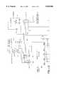
- FIG. 1is a block diagram of the instruction execution unit of the microprocessor of the present invention, showing the elements of the register file.
- FIGS. 2,2a, 3,3a and 4are simplified schematic and block diagrams of the floating point, integer and Boolean portions of the instruction execution unit of FIG. 1, respectively.
- FIGS. 5-6are more detailed views of the floating point and integer portions, respectively, showing the means for selecting between register sets.
- FIG. 7illustrates the fields of an exemplary microprocessor instruction word executable by the instruction execution unit of FIG. 1.
- FIG. 1illustrates the basic components of the instruction execution unit (IEU) 10 of the RISC (reduced instruction set computing) processor of the present invention.
- the IEU 10includes a register file 12 and an execution engine 14.
- the register file 12includes one or more register banks 16-0 to 16-n. It will be understood that the structure of each register bank 16 is identical to all of the other register banks 16. Therefore, the present application will describe only register bank 16-0.
- the register bankincludes a register set A 18, a register set FB 20, and a register set C 22.
- the inventionmay be characterized as a RISC microprocessor having a register file optimally configured for use in the execution of RISC instructions, as opposed to conventional register files-which are sufficient for use in the execution of CISC (complex instruction set computing) instructions by CISC processors.
- CISCcomplex instruction set computing
- the execution engine of the microprocessor's IEUachieves greatly improved performance, both in terms of resource utilization and in terms of raw throughput.
- the general conceptis to tune a register set to a RISC instruction, while the specific implementation may involve any of the register sets in the architecture.
- Register set A 18includes integer registers 24 (RA 31:0!), each of which is adapted to hold an integer value datum. In one embodiment, each integer may be thirty-two bits wide.
- the RA ! integer registers 24include a first plurality 26 of integer registers (RA 23:0!) and a second plurality 28 of integer registers (RA 31:24!).
- the RA ! integer registers 24are each of identical structure, and are each addressable in the same manner, albeit with a unique address within the integer register set 24. For example, a first integer register 30 (RA 0!) is addressable at a zero offset within the integer register set 24.
- RA 0!always contains the value zero. It has been observed that user applications and other programs use the constant value zero more than any other constant value. It is, therefore, desirable to have a zero readily available at all times, for clearing, comparing, and other purposes. Another advantage of having a constant, hard-wired value in a given register, regardless of the particular value, is that the given register may be used as the destination of any instruction whose results need not be saved.
- a data dependencyexists when a "slave" instruction requires, for one or more of its operands, the result of a "master" instruction. In a pipelined processor, this may cause pipeline stalls. For example, the master instruction, although occurring earlier in the code sequence than the slave instruction, may take considerably longer to execute. It will be readily appreciated that if a slave "increment and store" instruction operates on the result data of a master wquadruple-word integer divide instruction, the slave instruction will be fetched, decoded, and awaiting execution many clock cycles before the master instruction has finished execution.
- the numerical result of a master instructionis not needed, and the master instruction is executed for some other purpose only, such as to set condition code flags. If the master instruction's destination is RA 0!, the numerical results will be effectively discarded.
- the data dependency checker (not shown) of the IEU 10will not cause the slave instruction to be delayed, as the ultimate result of the master instruction--zero--is already known.
- the integer register set A 24also includes a set of shadow registers 32 (RT 31:24!). Each shadow register can hold an integer value, and is, in one embodiment, also thirty-two bits wide. Each shadow register is addressable as an offset in the same manner in which each integer register is addressable.
- the register set Aincludes an IEU mode integer switch 34.
- the switch 34like other such elements, need not have a physical embodiment as a switch, so long as the corresponding logical functionality is provided within the register sets.
- the IEU mode integer switch 34is coupled to the first subset 26 of integer registers on line 36, to the second subset of integer registers 28 on line 38, and to the shadow registers 32 on line 40. All accesses to the register set A 18 are made through the IEU mode integer switch 34 on line 42. Any access request to read or write a register in the first subset RA 23:0! is passed automatically through the IEU mode integer switch 34. However, accesses to an integer register with an offset outside the first subset RA 23:0! will be directed either to the second subset RA 31:24! or the shadow registers RT 31;24!, depending upon the operational mode of the execution engine 14.
- the IEU mode integer switch 34is responsive to a mode control unit 44 in the execution engine 14.
- the mode control unit 44provides pertinent state or mode information about the IEU 10 to the IEU mode integer switch 34 on line 46.
- the mode control unit 44controls the IEU mode integer switch 34 such that any requests to the second subset RA 31:24! are re-directed to the shadow RT 31:24!, using the same requested offset within the integer set. Any operating system kernel or other then-executing entity may thus have apparent access to the second subset RA 31:24! without the otherwise-required overhead of swapping the contents of the second subset RA 31:24! out to main memory, or pushing the second subset RA 31:24! onto a stack, or other conventional register-saving technique.
- the mode control unit 44controls the IEU mode integer switch 34 such that access is again directed to the second subset RA 31:24!.
- the mode control unit 44is responsive to the present state of interrupt enablement in the IEU 10.
- the execution engine 14includes a processor status register (PSR) (not shown), which includes a one-bit flag (PSR 7! indicating whether interrupts are enabled or disabled.
- the line 46may simply couple the IEU mode integer switch 34 to the interrupts-enabled flag in the PSR. While interrupts are disabled, the IEU 10 maintains access to the integers RA 23:0!, in order that it may readily perform analysis of various data of the user application. This may allow improved debugging, error reporting, or system performance analysis.
- the re-typable register set FB 20may be thought of as including floating point registers 48 (RF 31:0!); and/or integer registers 50 (RB 31:0!). When neither data type is implied to the exclusion of the other, this application will use the term RFB !.
- the floating point registers RF !occupy the same physical silicon space as the integer registers RB !.
- the floating point registers RF !are sixty-four bits wide and the integer registers RB ! are thirty-two bits wide. It will be understood that if double-precision floating point numbers are not required, the register set RFB ! may advantageously be constructed in a thirty-two-bit width to save the silicon area otherwise required by the extra thirty-two bits of each floating point register.
- Each individual register in the register set RFB !may hold either a floating point value or an integer value.
- the register set RFB !may include optional hardware for preventing accidental access of a floating point value as though it were an integer value, and vice versa. In one embodiment, however, in the interest of simplifying the register set RFB !, it is simply left to the software designer to ensure that no erroneous usages of individual registers are made.
- the execution engine 14simply makes an access request on line 52, specifying an offset into the register set RFB !, without specifying whether the register at the given offset is intended to be used as a floating point register or an integer register.
- various entitiesmay use either the full sixty-four bits provided by the register set RFB !, or may use only the low order thirty-two bits, such as in integer operations or single-precision floating point operations.
- a first register RFB 0! 51contains the constant value zero, in a form such that RB 0! is a thirty-two-bit integer zero (0000 hex ) and RF 0! is a sixty-four-bit floating point zero (00000000 hex ) This provides the same advantages as described above for RA 0!.
- the register set C 22includes a plurality of Boolean registers 54 (RC 31:0!). RC ! is also known as the "condition status register” (CSR).
- the Boolean registers RC !are each identical in structure and addressing, albeit that each is individually addressable at a unique address or offset within RC !.
- register set Cfurther includes a "previous condition status register” (PCSR) 60
- the register set Calso includes a CSR selector unit 62, which is responsive to the mode control unit 44 to select alternatively between the CSR 54 and the PCSR 60.
- the CSRis used when interrupts are enabled, and the PCSR is used when interrupts are disabled.
- the CSR and PCSPare identical in all other respects.
- the CSR selector unit 62pushes the contents of the CSR into the PCSR, overwriting the former contents of the PCSR, and when interrupts are re-enabled, the CSR selector unit 62 pops the contents of the PCSR back into the CSR.
- it may be desirable to merely alternate access between the CSR and the PCSRas is done with RA 31:24! and RT 31:24!.
- the PCSRis always available as a thirty-two-bit "special register”.
- Boolean registersare a dedicated condition flag, unlike the Boolean registers in previously known microprocessors. That is, the CSR 54 does not include a dedicated carry flag, nor a dedicated a minus flag, nor a dedicated flag indicating equality of a comparison or a zero subtraction result. Rather, any Boolean register may be the destination of the Boolean result of any Boolean operation. As with the other register sets, a first Boolean register 58 (RC 0! always contains the value zero, to obtain the advantages explained above for RA 0!. In the preferred embodiment, each Boolean register is one bit wide, indicating one Boolean value.
- the execution engine 14includes one or more integer functional units 66, one or more floating point functional units 68, and one or more Boolean functional units 70.
- the functional unitsexecute instructions as will be explained below.
- Buses 72, 73, and 75connect the various elements of the IEU 10, and will each be understood to represent data, address, and control paths.
- FIG. 7illustrates one exemplary format for an integer instruction which the execution engine 14 may execute. It will be understood that not all instructions need to adhere strictly to the illustrated format, and that the data processing system includes an instruction fetcher and decoder (not shown) which are adapted to operate upon varying format instructions. The single example of FIG. 7 is for ease in explanation only. Throughout this Application the identification I ! will be used to identify various bits of the instruction. I 31:30! are reserved for future implementations of the execution engine 14. I 29:26! identify the Instruction class of the particular instruction.
- Table 1shows the various classes of instructions performed by the present invention.
- Instruction classes of particular interest to this Applicationinclude the Class 0-3 register-to-register instructions and the Class 13 Boolean operations. While other classes of instructions also operate upon the register file 12, further discussion of those classes is not believed necessary in order to fully understand the present invention.
- I 25!is identified as B0, and indicates whether the destination register is in register set A or register set B.
- I 24:22!are an opcode which identifies, within the given instruction class, which specific function is to be performed. For example, within the register-to-register classes, an opcode may specify "addition".
- I 21!identifies the addressing mode which is to be used when performing the instruction--either register source addressing or immediate source addressing.
- I 20:16!identify the destination register as an offset within the register set indicated by B0.
- I 15!is identified as B1 and indicates whether the first operand is to be taken from register set A or register set B.
- I 14:10!identify the register offset It from which the first operand is to be taken.
- I 24:22!identify a function selection--an extension of the opcode I 24:22!. I 7:6! are reserved. I 1! is identified as B2 and indicates whether a second operand of the instruction is to be taken from register set A or register set B. Finally, I 4:0! identify the register offset from which the second operand is to be taken.
- the integer functional unit 66 and floating point functional unit 68are equipped to perform integer comparison instructions and floating point comparisons, respectively.
- the instruction format for the comparison instructionis substantially identical to that shown in FIG. 7, with the caveat that various fields may advantageously be identified by slightly different names.
- I 20:16!identifies the destination register where the result is to be stored, but the addressing mode field I 21! does not select between register sets A or B. Rather, the addressing mode field indicates whether the second source of the comparison is found in a register or is immediate data. Because the comparison is a Boolean type instruction, the destination register is always found in register set C. All other fields function as shown in FIG. 7.
- the opcode and function select fieldsidentify which Boolean condition is to be tested for in comparing the two operands.
- the integer and the floating point functional unitsfully support the IEEE standards for numerical comparisons.
- the IEU 10is a load/store machine. This means that when the contents of a register are stored to memory or read from memory, an address calculation must be performed in order to determine which location in memory is to be the source or the destination of the store or load, respectively.
- the destination register field I 20:16!identifies the register which is the destination or the source of the load or store, respectively.
- the source register 1 field, I 14:10!identifies a register in either set A or B which contains a base address of the memory location.
- the source register 2 field, I 4:0!identifies a register in set A or set B which contains an index or an offset from the base.
- the load/store addressis calculated by adding the index to the base.
- I 7:0!include immediate data which are to be added as an index to the base.
- integer functional unit 66the floating point functional unit 68, and the Boolean functional unit 70 are responsive to the contents of the instruction class field, the opcode field, and the function select field of a present instruction being executed.
- the integer functional unitmay be responsive thereto to perform the indicated operation, while the floating point functional unit and the Boolean functional unit may be responsive thereto to not perform the operation.
- the floating point functional unit 68is equipped to perform both floating point and integer operations.
- the functional unitsare constructed to each perform more than one instruction simultaneously.
- the integer functional unit 66performs integer functions only. Integer operations typically involve a first source, a second source, and a destination. A given integer instruction will specify a particular operation to be performed on one or more source operands and will specify that the result of the integer operation is to be stored at a given destination. In some instructions, such as address calculations employed in load/store operations, the sources are utilized as a base and an index.
- the integer functional unit 66is coupled to a first bus 72 over which the integer functional unit 66 is connected to a switching and multiplexing control (SMC) unit A 74 and an SMC unit B 76. Each integer instruction executed by the integer functional unit 66 will specify whether each of its sources and destination reside in register set A or register set B.
- SMCswitching and multiplexing control
- the IEU 10has received, from the instruction fetch unit (not shown), an instruction to perform an integer register-to-register addition.
- the instructionmay specify a register bank, perhaps even a separate bank for each source and destination.
- the instruction I !is limited to a thirty-two-bit length, and does not contain any indication of which register bank 16-0 through 16-n is involved in the instruction. Rather, the bank selector unit 78 controls which register bank is presently active. In one embodiment, the bank selector unit 78 is responsive to one or more bank selection bits in a status word (not shown) within the IEU 10.
- the integer functional unit 66is responsive to the identification in I 14:10! and I 4:0! of the first and second source registers.
- the integer functional unit 66places an identification of the first and second source registers at ports S1 and S2, respectively, onto the integer functional unit bus 72 which is coupled to both SMC units A and B 74 and 76.
- the SMC units A and Bare each coupled to receive B0-2 from the instruction I !.
- a zero in any respective Bnindicates register set A, and a one indicates register set B.
- the source ports of the integer and floating point functional units 66 and 68are utilized as a base port and an index port, B and I, respectively.
- the integer functional unit 66After obtaining the first and second operands from the indicated register sets on the bus 72, as explained below, the integer functional unit 66 performs the indicated operation upon those operands, and provides the result at port D onto the integer functional unit bus 72.
- the SMC units A and Bare responsive to B0 to route the result to the appropriate register set A or B.
- the SMC unit Bis further responsive to the instruction class opcode, and function selection to control whether operands are read from (or results are stored to) either a floating point register RF ! or an integer register RB !.
- the registers RF !may be sixty-four bits wide while the registers are RB ! are only thirty-two bits wide.
- SMC unit Bcontrols whether a word or a double word is written to the register set RFB !. Because all registers within register set A are thirty-two bits wide, SMC unit A need not include means for controlling the width of data transfer on the bus 42.
- the IEU mode integer switch 34is responsive to the mode control unit 44 of the execution engine 14 to control whether data on the bus 42 are connected through to bus 36, bus 38 or bus 40, and vice versa.
- IEU mode integer switch 34is further responsive to I 20:16!, I 14:10!, and I 4:0!. If a given indicated destination or source is in RA 23:0!, the IEU mode integer switch 34 automatically couples the data between lines 42 and 36. However, for registers RA 31:24!, the IEU mode integer switch 34 determines whether data on line 42 is connected to line 38 or line 40, and vice versa. When interrupts are enabled, IEU mode integer switch 34 connects the SMC unit A to the second subset 28 of integer registers RA 31:24!. When interrupts are disabled, the IEU mode integer switch 34 connects the SMC unit A to the shadow registers RT 31:24!.
- an instruction executing within the integer functional unit 66need not be concerned with whether to address RA 31:24! or RT 31:24!. It will be understood that SMC unit A may advantageously operate identically whether it is being accessed by the integer functional unit 66 or by the floating point functional unit 68.
- the floating point functional unit 68is responsive to the class, opcode, and function select fields of the instruction, to perform floating point operations.
- the S1, S2, and D portsoperate as described for the integer functional unit 66.
- SMC unit Bis responsive to retrieve floating point operands from, and to write numerical floating point results to, the floating point registers RF ! on bus 52.
- SMC unit C 80is responsive to the instruction class, opcode, and function select fields of the instruction I !.
- SMC unit Cdetects that a comparison operation has been performed by one of the numerical functional units 66 or 68, it writes the Boolean result over bus 56 to the Boolean register indicated at the D port of the functional unit which performed the comparison.
- the Boolean functional unit 70does not perform comparison instructions as do the integer and floating point functional units 66 and 68. Rather, the Boolean functional unit 70 is only used in performing bitwise logical combination of Boolean register contents, according to the Boolean functions listed in Table 2.
- Table 3illustrates an example of a segment of code which performs a conditional branch based upon a complex Boolean function.
- the complex Boolean functionincludes three portions which are OR-ed together. The first portion includes two sub-portions, which are AND-ed together.
- Table 4illustrates, in pseudo-assembly form, one likely method by which previous microprocessors would perform the function of Table 3.
- the code in Table 4is written as though it were constructed by a compiler of at least normal intelligence operating upon the code of Table 3. That is, the compiler will recognize that the condition expressed in lines 2-4 of Table 3 is passed if any of the three portions is true.
- the assignment at line 1 of Table 3is performed by the "load immediate" statement at line 1 of Table 4.
- the first portion of the complex Boolean condition, expressed at line 2 of Table 3,is represented by the statements in lines 2-5 of Table 4.
- the compare statement at line 2 of Table 4performs a subtraction of RA 2! from RA 3! or vice versa, depending upon the implementation, and may or may not store the result of that subtraction.
- the important function performed by the comparison statementis that the zero, minus, and carry flags will be appropriately set or cleared.
- conditional branch statement at line 3 of Table 4branches to a subsequent portion of code upon the condition that RA 2! did not equal RA 3!. If the two were unequal, the zero flag will be clear, and there is no need to perform the second sub-portion.
- the existence of the conditional branch statement at line 3 of Table 4prevents the further fetching, decoding, and executing of any subsequent statement in Table 4 until the results of the comparison in line 2 are known, causing a pipeline stall. If the first sub-portion of the first portion (TEST1) is passed, the second sub-portion at line 4 of Table 4 then compares RA 4!to RA 5!, again setting and clearing the appropriate status flags.
- the second portion of the Boolean functionis the comparison of RA 6! to RA 7!, at line 6 of Table 4, which again sets and clears the appropriate status flags. If the condition "less than” is indicated by the status flags, the complex Boolean function is passed, and execution may immediately branch to the DO -- IF label. In various prior microprocessors, the "less than” condition may be tested by examining the minus flag. If RA 7! was not less than RA 6!, the third portion of the test must be performed. The statement at line 8 of Table 4 compares RA 8! to RA 9!.
- the Boolean register set Callows the microprocessor to perform the three test portions back-to-back without intervening branching.
- Each Boolean comparisonspecifies two operands, a destination, and a Boolean condition for which to test.
- the comparison at line 2 of Table 5compares the contents of RA 2! to the contents of RA 3!, tests them for equality, and stores into RC 11! the Boolean value of the result of the comparison.
- each comparison of the Boolean functionstores its respective intermediate results in a separate Boolean register.
- the IEU 10is capable of simultaneously performing more than one of the comparisons.
- the Boolean functional unit 70is responsive to the instruction class, opcode, and function select fields as are the other functional units. Thus, it will be understood with reference to Table 5 again, that the integer and/or floating point functional units will perform the instructions in lines 1-5 and 13, and the Boolean functional unit 70 will perform the Boolean bitwise combination instructions in lines 6-8.
- the control flow and branching instructions in line 9-12will be performed by elements of the IEU 10 which are not shown in FIG. 1.
- FIGS. 2-5illustrate further details of the data paths within the floating point, integer, and Boolean portions of the IEU, respectively.
- the register set FB 20is a multi-ported register set.
- the register set FB 20has two write ports WFB0-1, and five read ports RDFB0-4.
- The-floating point functional unit 68 of FIG. 1is comprised of the ALU2 102, FALU 104, MULT 106, and NULL 108 of FIG. 2. All elements of FIG. 2 except the register set 20 and the elements 102-108 comprise the SMC unit B of FIG. 1.
- External, bidirectional data bus EX -- DATA !provides data to the floating point load/store unit 122.
- Immediate floating point data bus LDF -- IMED !provides data from a "load immediate” instruction.
- Other immediate floating point dataare provided on busses RFF1 13 IMED and RFF2 -- IMED, such as is involved in an "add immediate” instruction.
- Dataare also provided on bus EX -- SR -- DT !, in response to a "special register move" instruction. Data may also arrive from the integer portion, shown in FIG. 3, on busses 114 and 120.
- the floating point register set's two write ports WFB0 and WFB1are coupled to write multiplexers 110-0 and 110-1, respectively.
- the write multiplexers 110receive data from: the ALU0 or SHF0 of the integer portion of FIG. 3; the FALU; the MULT; the ALU2; either EX -- SR -- DT ! or LDF -- IMED !; and EX -- DATA !.
- control signals(not shown) determine which input is selected at each port, and address signals (not shown) determine to which register the input data are written.
- Multiplexer control and register addressingare within the skill of persons in the art, and will not be discussed for any multiplexer or register set in the present invention.
- the floating point register set's five read ports RDFB0 to RDFB4are coupled to read multiplexers 112-0 to 112-4, respectively.
- the read multiplexerseach also receives data from: either EX -- SR -- DT ! or LDF -- IMED !, on load immediate bypass bus 126; a load external data bypass bus 127, which allows external load data to skip the register set FB; the output of the ALU2 102, which performs non-multiplication integer operations; the FALU 104, which performs non-multiplication floating point operations; the MULT 106, which performs multiplication operations; and either the ALU0 140 or the SHF0 144 of the integer portion shown in FIG. 3, which respectively perform non-multiplication integer operations and shift operations.
- Read multiplexers 112-1 and 112-3also receive data from RFF1 -- IMED ! and RFF2 -- IMED !, respectively.
- Each arithmetic-type unit 102-106 in the floating point portionreceives two inputs, from respective sets of first and second source multiplexers S1 and S2.
- the first source of each unit ALU2, FALU, and MULTcomes from the output of either read multiplexer 112-0 or 112-2, and the second source comes from the output of either read multiplexer 112-1 or 112-3.
- the sources of the FALU and the MULTmay also come from the integer portion of FIG. 3 on bus 114.
- the results of the ALU2, FALU, and MULTare provided back to the write multiplexers 110 for storage into the floating point registers RF !, and also to the read multiplexers 112 for re-use as operands of subsequent operations.
- the FALUalso outputs a signal FALU -- BD indicating the Boolean result of a floating point comparison operation.
- FALU -- BDis calculated directly from internal zero and sign flags of the FALU.
- Null byte tester NULL 108performs null byte testing operations upon an operand from a first source multiplexer, in one mode that of the ALU2. NULL 108 outputs a Boolean signal NULLB -- BD indicating whether the thirty-two-bit first source operand includes a byte of value zero.
- the outputs of read multiplexers 112-0, 112-1, and 112-4are provided to the integer portion (of FIG. 3) on bus 118.
- the output of read multiplexer 112-4is also provided as STDT -- FP ! store data to the floating point load/store unit 122.
- FIG. 5illustrates further details of the control of the S1 and S2 multiplexers.
- each S1 multiplexermay be responsive to bit B1 of the instruction I !, and each S2 multiplexer may be responsive to bit B2 of the instruction I !.
- the S1 and S2 multiplexersselect the sources for the various functional units.
- the sourcesmay come from either of the register files, as controlled by the B1 and B2 bits of the instruction itself.
- each register fileincludes two read ports from which the sources may come, as controlled by hardware not shown in the FIGS.
- the register set A 18is also multi-ported.
- the register set A 18has two write ports WA0-1, and five read ports RDA0-4.
- the integer functional unit 66 of FIG. 1is comprised of the ALU0 140, ALU1 142, SHF0 144, and NULL 146 of FIG. 3. All elements of FIG. 3 except the register set 18 and the elements 140-146 comprise the SMC unit A of FIG. 1.
- External data bus EX -- DATA !provides data to the integer load/store unit 152.
- Immediate integer data on bus LDI -- IMED !are provided in response to a "load immediate” instruction.
- Other immediate integer dataare provided on busses RFA1 -- IMED and RFA2 -- IMED in response to non-load immediate instructions, such as an "add immediate”.
- Dataare also provided on bus EX -- SR -- DT ! in response to a "special register move" instruction. Data may also arrive from the floating point portion (shown in FIG. 2) on busses 116 and 118.
- the integer register set's two write ports WA0 and WA1are coupled to write multiplexers 148-0 and 148-1, respectively.
- the write multiplexers 148receive data from: the FALU or MULT of the floating point portion (of FIG. 2); the ALU0; the ALU1; the SHF0; either EX -- SR -- DT ! or LDI -- IMED !; and EX -- DATA !.
- the integer register set's five read ports RDA0 to RDA4are coupled to read multiplexers 150-0 to 150-4, respectively.
- Each read multiplexeralso receives data from: either EX -- SR -- DT ! or LDI -- IMED ! on load immediate bypass bus 160; a load external data bypass bus 154, which allows external load data to skip the register set A; ALU0; ALU1; SHF0; and either the FALU or the MULT of the floating point portion (of FIG. 2).
- Read multiplexers 150-1 and 150-3also receive data from RFA1 -- IMED ! and RFA2 -- IMED !, respectively.
- Each arithmetic-type unit 140-144 in the integer portionreceives two inputs, from respective sets of first and second source multiplexers S1 and S2.
- the first source of ALU0comes from either the output of read multiplexer 150-2, or a thirty-two-bit wide constant zero (0000 hex ) or floating point read multiplexer 112-4.
- the second source of ALU0comes from either read multiplexer 150-3 or floating point read multiplexer 112-1.
- the first source of ALU1comes from either read multiplexer 150-0 or IF -- PC !. IF -- PC ! is used in calculating a return address needed by the instruction fetch unit (not shown), due to the IEU's ability to perform instructions in an out-of-order sequence.
- the second source of ALULcomes from either read multiplexer 150-1 or CF -- OFFSET !. CF -- OFFSET ! is used in calculating a return address for a CALL instruction, also due to the out-of-order capability.
- the first source of the shifter SHF0 144is from either: floating point read multiplexer 112-0 or 112-4; or any integer read multiplexer 150.
- the second source of SHF0is from either: floating point read multiplexer 112-0 or 112-4; or integer read multiplexer 150-0, 150-2, or 150-4.
- SHF0takes a third input from a shift amount multiplexer (SA). The third input controls how far to shift, and is taken by the SA multiplexer from either: floating point read multiplexer 112-1; integer read multiplexer 150-1 or 150-3; or a five-bit wide constant thirty-one (11111 2 or 31 10 ).
- the shifter SHF0requires a fourth input from the size multiplexer (S). The fourth input controls how much data to shift, and is taken by the S multiplexer from either: read multiplexer 150-1; read multiplexer 150-3; or a five-bit wide constant sixteen (10000 2 or 16 10 ).
- the results of the ALU0, ALU1, and SHF0are provided back to the write multiplexers 148 for storage into the integer registers RA !, and also to the read multiplexers 150 for re-use as operands of subsequent operations.
- the output of either ALU0 or SHF0is provided on bus 120 to the floating point portion of FIG. 3.
- the ALU0 and ALU1also output signals ALU0 -- BD and ALU1 -- BD, respectively, indicating the Boolean results of integer comparison operations.
- ALU0 -- BD and ALU1 -- BDare calculated directly from the zero and sign flags of the respective functional units.
- ALU0also outputs signals EX -- TADR ! and EX -- VM -- ADR. EX -- TADR !
- EX -- VM -- ADR !is the virtual address used for all loads from memory and stores to memory, and is sent to the VMU (not shown) for address translation.
- Null byte tester NULL 146performs null byte testing operations upon an operand from a first source multiplexer.
- the operandis from the ALU0.
- NULL 146outputs a Boolean signal NULLA -- BD indicating whether the thirty-two-bit first source operand includes a byte of value zero.
- the outputs of read multiplexers 150-0 and 150-1are provided to the floating point portion (of FIG. 2) on bus 114.
- the output of read multiplexer 150-4is also provided as STDT -- INT ! store data to the integer load/store unit 152.
- a control bit PSR 7!is provided to the register set A 18. It is this signal which, in FIG. 1, is provided from the mode control unit 44 to the IEU mode integer switch 34 on line 46.
- the IEU mode integer switchis internal to the register set A 18 as shown in FIG. 3.
- FIG. 6illustrates further details of the control of the S1 and S2 multiplexers.
- the signal ALU0 -- BDALU0 -- BD
- the register set C 22is also multi-ported.
- the register set C 22has two write-ports WC0-1, and five read ports RDA0-4. All elements of FIG. 4 except the register set 22 and the Boolean combinational unit 70 comprise the SMC unit C of FIG. 1.
- the Boolean register set's two write ports WC0 and WC1are coupled to write multiplexers 170-0 and 170-1, respectively.
- the write multiplexers 170receive data from the output of the Boolean combinational unit 70, indicating the Boolean result of a Boolean combinational operation; ALU0 -- BD from the integer portion of FIG. 3, indicating the Boolean result of an integer comparison; FALU -- BD from the floating point portion of FIG.
- ALU1 -- BD -- Pfrom ALU1, indicating the results of a compare instruction in ALU1, or NULLA -- BD from NULL 146, indicating a null byte in the integer portion
- ALU2 -- BD -- Pfrom ALU2, indicating the results of a compare operation in ALU2, or NULLB -- BD from NULL 108, indicating a null byte in the floating point portion.
- the ALU0 -- BD, ALU1 -- BD, ALU2 -- BD, and FALU -- BD signalsare not taken from the data paths, but are calculated as a function of the zero flag, minus flag, carry flag, and other condition flags in the PSR.
- the IEUmaintains up to eight PSRs.
- the Boolean register set Cis also coupled to bus EX -- SR -- DT !, for use with "special register move" instructions.
- the CSRmay be written or read as a whole, as though it were a single thirty-two-bit register. This enables rapid saving and restoration of machine state information, such as may be necessary upon certain drastic system errors or upon certain forms of grand scale context switching.
- the Boolean register set's five read ports RDC0 to RDC3are coupled to read multiplexers 172-0 to 172-4, respectively.
- the read multiplexers 172receive the same set of inputs as the write multiplexers 170 receive.
- the Boolean combinational unit 70receives inputs from read multiplexers 170-0 and 170-1.
- Read multiplexers 172-2 and 172-3respectively provide signals BLBP -- CPORT and BLBP -- DPORT.
- BLBP -- CPORTis used as the basis for conditional branching instructions in the IEU.
- BLBP -- DPORTis used in the "add with Boolean" instruction, which sets an integer register in the A or B set to zero or one (with leading zeroes), depending upon the content of a register in the C set.
- Read port RDC4is presently unused, and is reserved for future enhancements of the Boolean functionality of the IEU.
Landscapes
- Engineering & Computer Science (AREA)
- Software Systems (AREA)
- Theoretical Computer Science (AREA)
- Physics & Mathematics (AREA)
- General Engineering & Computer Science (AREA)
- General Physics & Mathematics (AREA)
- Mathematical Physics (AREA)
- Multimedia (AREA)
- Executing Machine-Instructions (AREA)
- Advance Control (AREA)
Abstract
Description
TABLE 1 ______________________________________ Instruction Classes Class Instructions ______________________________________ 0-3 Integer and floating point register-to-register instructions 4 Immediateconstant load 5 Reserved 6Load 7 Store 8-11Control Flow 12 Modifier 13Boolean operations 14 Reserved 15 Atomic (extended) ______________________________________
TABLE 2 ______________________________________ Boolean Functions I 23,22,9,8! Boolean result calculation ______________________________________ 0000 ZERO 0001 S1 AND S2 0010 S1 AND (NOT S2) 0011 S1 0100 (NOT S1) AND S2 0101 S2 0110S1 XOR 52 0111 S1 OR S2 1000 S1 NOR S2 1001 S1 XNOR S2 1010 NOT S2 1011 S1 OR (NOT S2) 1100 NOT S1 1101 (NOT S1) OR S2 1110 S1 NAND S2 1111 ONE ______________________________________
TABLE 3 ______________________________________ Example of Complex Boolean Function ______________________________________ 1RA 1! := 0; 2 IF (((RA 2! =RA 3!) AND (RA 4! >RA 5!)) OR 3 (RA 6! <RA 7!) OR 4 (RA 8! <>RA 9!)) THEN 5 X() 6 ELSE 7 Y(); 8RA 10! := 1; ______________________________________
TABLE 4 ______________________________________ Execution of Complex Boolean Function Without Boolean Register Set ______________________________________ 1START LDI RA 1!,0 2TEST1 CMP RA 2!,RA 3! 3BNE TEST2 4CMP RA 4!,RA 5! 5 BGT DO.sub.-- IF 6TEST2 CMP RA 6!,RA 7! 7 BLT DO.sub.-- IF 8TEST3 CMP RA 8!,RA 9! 9 BEQ DO.sub.-- ELSE 10 DO.sub.-- IF JSR ADDRESS OF X() 11 JMP PAST.sub.-- ELSE 12 DO.sub.-- ELSE JSR ADDRESS OF Y() 13 PAST.sub.-- ELSELDI RA 10!,1 ______________________________________
TABLE 5 ______________________________________ Execution of Complex Boolean Function With Boolean Register Set ______________________________________ 1START LDI RA 1!,0 2 TEST1 CMP RC 11!,RA 2!,RA 3!,EQ 3CMP RC 12!,RA 4!,RA 5!,GT 4 TEST2 CMP RC 13!,RA 6!,RA 7!,LT 5TEST3 CMP RC 14!,RA 8!,RA 9!,NE 6 COMPLEX ANDRC 15!,RC 11!,RC 12! 7 ORRC 16!,RC 13!,RC 14! 8 OR RC 17!,RC 15!,RC 16! 9 BC RC 17!,DO.sub.-- ELSE 10 DO.sub.-- IF JSR ADDRESS OF X() 11 JMP PAST.sub.-- ELSE 12 DO.sub.-- ELSE JSR ADDRESS OF Y() 13 PAST.sub.-- ELSELDI RA 10!,1 ______________________________________
Claims (30)
Priority Applications (7)
| Application Number | Priority Date | Filing Date | Title |
|---|---|---|---|
| US08/937,361US5838986A (en) | 1991-07-08 | 1997-09-25 | RISC microprocessor architecture implementing multiple typed register sets |
| US09/188,708US6044449A (en) | 1991-07-08 | 1998-11-10 | RISC microprocessor architecture implementing multiple typed register sets |
| US09/480,136US6249856B1 (en) | 1991-07-08 | 2000-01-10 | RISC microprocessor architecture implementing multiple typed register sets |
| US09/840,026US20010034823A1 (en) | 1991-07-08 | 2001-04-24 | RISC microprocessor architecture implementing multiple register sets |
| US10/060,086US7555631B2 (en) | 1991-07-08 | 2002-01-31 | RISC microprocessor architecture implementing multiple typed register sets |
| US11/651,009US7685402B2 (en) | 1991-07-08 | 2007-01-09 | RISC microprocessor architecture implementing multiple typed register sets |
| US12/650,998US7941636B2 (en) | 1991-07-08 | 2009-12-31 | RISC microprocessor architecture implementing multiple typed register sets |
Applications Claiming Priority (4)
| Application Number | Priority Date | Filing Date | Title |
|---|---|---|---|
| US07/726,773US5493687A (en) | 1991-07-08 | 1991-07-08 | RISC microprocessor architecture implementing multiple typed register sets |
| US08/465,239US5560035A (en) | 1991-07-08 | 1995-06-05 | RISC microprocessor architecture implementing multiple typed register sets |
| US08/665,845US5682546A (en) | 1991-07-08 | 1996-06-19 | RISC microprocessor architecture implementing multiple typed register sets |
| US08/937,361US5838986A (en) | 1991-07-08 | 1997-09-25 | RISC microprocessor architecture implementing multiple typed register sets |
Related Parent Applications (1)
| Application Number | Title | Priority Date | Filing Date |
|---|---|---|---|
| US08/665,845ContinuationUS5682546A (en) | 1991-07-08 | 1996-06-19 | RISC microprocessor architecture implementing multiple typed register sets |
Related Child Applications (1)
| Application Number | Title | Priority Date | Filing Date |
|---|---|---|---|
| US09/188,708ContinuationUS6044449A (en) | 1991-07-08 | 1998-11-10 | RISC microprocessor architecture implementing multiple typed register sets |
Publications (1)
| Publication Number | Publication Date |
|---|---|
| US5838986Atrue US5838986A (en) | 1998-11-17 |
Family
ID=24919957
Family Applications (10)
| Application Number | Title | Priority Date | Filing Date |
|---|---|---|---|
| US07/726,773Expired - LifetimeUS5493687A (en) | 1991-07-08 | 1991-07-08 | RISC microprocessor architecture implementing multiple typed register sets |
| US08/465,239Expired - LifetimeUS5560035A (en) | 1991-07-08 | 1995-06-05 | RISC microprocessor architecture implementing multiple typed register sets |
| US08/665,845Expired - LifetimeUS5682546A (en) | 1991-07-08 | 1996-06-19 | RISC microprocessor architecture implementing multiple typed register sets |
| US08/937,361Expired - LifetimeUS5838986A (en) | 1991-07-08 | 1997-09-25 | RISC microprocessor architecture implementing multiple typed register sets |
| US09/188,708Expired - Fee RelatedUS6044449A (en) | 1991-07-08 | 1998-11-10 | RISC microprocessor architecture implementing multiple typed register sets |
| US09/480,136Expired - Fee RelatedUS6249856B1 (en) | 1991-07-08 | 2000-01-10 | RISC microprocessor architecture implementing multiple typed register sets |
| US09/840,026AbandonedUS20010034823A1 (en) | 1991-07-08 | 2001-04-24 | RISC microprocessor architecture implementing multiple register sets |
| US10/060,086Expired - Fee RelatedUS7555631B2 (en) | 1991-07-08 | 2002-01-31 | RISC microprocessor architecture implementing multiple typed register sets |
| US11/651,009Expired - Fee RelatedUS7685402B2 (en) | 1991-07-08 | 2007-01-09 | RISC microprocessor architecture implementing multiple typed register sets |
| US12/650,998Expired - Fee RelatedUS7941636B2 (en) | 1991-07-08 | 2009-12-31 | RISC microprocessor architecture implementing multiple typed register sets |
Family Applications Before (3)
| Application Number | Title | Priority Date | Filing Date |
|---|---|---|---|
| US07/726,773Expired - LifetimeUS5493687A (en) | 1991-07-08 | 1991-07-08 | RISC microprocessor architecture implementing multiple typed register sets |
| US08/465,239Expired - LifetimeUS5560035A (en) | 1991-07-08 | 1995-06-05 | RISC microprocessor architecture implementing multiple typed register sets |
| US08/665,845Expired - LifetimeUS5682546A (en) | 1991-07-08 | 1996-06-19 | RISC microprocessor architecture implementing multiple typed register sets |
Family Applications After (6)
| Application Number | Title | Priority Date | Filing Date |
|---|---|---|---|
| US09/188,708Expired - Fee RelatedUS6044449A (en) | 1991-07-08 | 1998-11-10 | RISC microprocessor architecture implementing multiple typed register sets |
| US09/480,136Expired - Fee RelatedUS6249856B1 (en) | 1991-07-08 | 2000-01-10 | RISC microprocessor architecture implementing multiple typed register sets |
| US09/840,026AbandonedUS20010034823A1 (en) | 1991-07-08 | 2001-04-24 | RISC microprocessor architecture implementing multiple register sets |
| US10/060,086Expired - Fee RelatedUS7555631B2 (en) | 1991-07-08 | 2002-01-31 | RISC microprocessor architecture implementing multiple typed register sets |
| US11/651,009Expired - Fee RelatedUS7685402B2 (en) | 1991-07-08 | 2007-01-09 | RISC microprocessor architecture implementing multiple typed register sets |
| US12/650,998Expired - Fee RelatedUS7941636B2 (en) | 1991-07-08 | 2009-12-31 | RISC microprocessor architecture implementing multiple typed register sets |
Country Status (7)
| Country | Link |
|---|---|
| US (10) | US5493687A (en) |
| EP (2) | EP0911724A3 (en) |
| JP (3) | JP3607701B2 (en) |
| KR (1) | KR100294964B1 (en) |
| AT (1) | ATE185205T1 (en) |
| DE (1) | DE69230057T2 (en) |
| WO (1) | WO1993001543A1 (en) |
Cited By (23)
| Publication number | Priority date | Publication date | Assignee | Title |
|---|---|---|---|---|
| US5949994A (en)* | 1997-02-12 | 1999-09-07 | The Dow Chemical Company | Dedicated context-cycling computer with timed context |
| US6044449A (en)* | 1991-07-08 | 2000-03-28 | Seiko Epson Corporation | RISC microprocessor architecture implementing multiple typed register sets |
| US6298431B1 (en)* | 1997-12-31 | 2001-10-02 | Intel Corporation | Banked shadowed register file |
| US6308261B1 (en)* | 1998-01-30 | 2001-10-23 | Hewlett-Packard Company | Computer system having an instruction for probing memory latency |
| US20020016903A1 (en)* | 1991-07-08 | 2002-02-07 | Nguyen Le Trong | High-performance, superscalar-based computer system with out-of-order instruction execution and concurrent results distribution |
| US20020019928A1 (en)* | 2000-03-08 | 2002-02-14 | Ashley Saulsbury | Processing architecture having a compare capability |
| WO2002069135A1 (en)* | 2001-02-21 | 2002-09-06 | Mips Technologies, Inc. | Partial bitwise permutations |
| US6668316B1 (en) | 1999-02-17 | 2003-12-23 | Elbrus International Limited | Method and apparatus for conflict-free execution of integer and floating-point operations with a common register file |
| US6766440B1 (en)* | 2000-02-18 | 2004-07-20 | Texas Instruments Incorporated | Microprocessor with conditional cross path stall to minimize CPU cycle time length |
| US6961846B1 (en)* | 1997-09-12 | 2005-11-01 | Infineon Technologies North America Corp. | Data processing unit, microprocessor, and method for performing an instruction |
| US20060053323A1 (en)* | 2000-09-20 | 2006-03-09 | Mips Technologies Inc. | Method and apparatus for disassociating power consumed within a processing system with instructions it is executing |
| WO2006120367A1 (en)* | 2005-05-11 | 2006-11-16 | Arm Limited | A data processing apparatus and method employing multiple register sets |
| US7318145B1 (en) | 2001-06-01 | 2008-01-08 | Mips Technologies, Inc. | Random slip generator |
| US7516305B2 (en) | 1992-05-01 | 2009-04-07 | Seiko Epson Corporation | System and method for retiring approximately simultaneously a group of instructions in a superscalar microprocessor |
| US7558945B2 (en) | 1992-12-31 | 2009-07-07 | Seiko Epson Corporation | System and method for register renaming |
| US7599981B2 (en) | 2001-02-21 | 2009-10-06 | Mips Technologies, Inc. | Binary polynomial multiplier |
| US7617388B2 (en) | 2001-02-21 | 2009-11-10 | Mips Technologies, Inc. | Virtual instruction expansion using parameter selector defining logic operation on parameters for template opcode substitution |
| US7711763B2 (en) | 2001-02-21 | 2010-05-04 | Mips Technologies, Inc. | Microprocessor instructions for performing polynomial arithmetic operations |
| US7739482B2 (en) | 1991-07-08 | 2010-06-15 | Seiko Epson Corporation | High-performance, superscalar-based computer system with out-of-order instruction execution |
| US7802074B2 (en) | 1992-03-31 | 2010-09-21 | Sanjiv Garg | Superscalar RISC instruction scheduling |
| US7860911B2 (en) | 2001-02-21 | 2010-12-28 | Mips Technologies, Inc. | Extended precision accumulator |
| US8074052B2 (en) | 1992-12-31 | 2011-12-06 | Seiko Epson Corporation | System and method for assigning tags to control instruction processing in a superscalar processor |
| US10255462B2 (en) | 2016-06-17 | 2019-04-09 | Arm Limited | Apparatus and method for obfuscating power consumption of a processor |
Families Citing this family (96)
| Publication number | Priority date | Publication date | Assignee | Title |
|---|---|---|---|---|
| US5371684A (en)* | 1992-03-31 | 1994-12-06 | Seiko Epson Corporation | Semiconductor floor plan for a register renaming circuit |
| US5640582A (en)* | 1992-05-21 | 1997-06-17 | Intel Corporation | Register stacking in a computer system |
| GB2286265B (en)* | 1994-01-26 | 1998-02-18 | Advanced Risc Mach Ltd | selectable processing registers |
| US5828856A (en)* | 1994-01-28 | 1998-10-27 | Apple Computer, Inc. | Dual bus concurrent multi-channel direct memory access controller and method |
| US5655151A (en)* | 1994-01-28 | 1997-08-05 | Apple Computer, Inc. | DMA controller having a plurality of DMA channels each having multiple register sets storing different information controlling respective data transfer |
| US5805927A (en)* | 1994-01-28 | 1998-09-08 | Apple Computer, Inc. | Direct memory access channel architecture and method for reception of network information |
| US5664159A (en)* | 1994-03-08 | 1997-09-02 | Exponential Technology, Inc. | Method for emulating multiple debug breakpoints by page partitioning using a single breakpoint register |
| US5734874A (en)* | 1994-04-29 | 1998-03-31 | Sun Microsystems, Inc. | Central processing unit with integrated graphics functions |
| KR100329338B1 (en) | 1994-12-02 | 2002-07-18 | 피터 엔. 데트킨 | Microprocessor with packing operation of composite operands |
| US6081880A (en)* | 1995-03-09 | 2000-06-27 | Lsi Logic Corporation | Processor having a scalable, uni/multi-dimensional, and virtually/physically addressed operand register file |
| US5713035A (en)* | 1995-03-31 | 1998-01-27 | International Business Machines Corporation | Linking program access register number with millicode operand access |
| US5966529A (en)* | 1995-05-15 | 1999-10-12 | Zsp Corporation | Processor having auxiliary operand register file and complementary arrangements for non-disruptively performing adjunct execution |
| US5812871A (en)* | 1995-06-30 | 1998-09-22 | Motorola Inc. | Data processing system and a method of optimizing an operation of the data processing system |
| JP3512272B2 (en)* | 1995-08-09 | 2004-03-29 | 株式会社日立製作所 | Comparison operation device and graphic operation system |
| US5742840A (en)* | 1995-08-16 | 1998-04-21 | Microunity Systems Engineering, Inc. | General purpose, multiple precision parallel operation, programmable media processor |
| US5953241A (en) | 1995-08-16 | 1999-09-14 | Microunity Engeering Systems, Inc. | Multiplier array processing system with enhanced utilization at lower precision for group multiply and sum instruction |
| US6643765B1 (en) | 1995-08-16 | 2003-11-04 | Microunity Systems Engineering, Inc. | Programmable processor with group floating point operations |
| US5900025A (en)* | 1995-09-12 | 1999-05-04 | Zsp Corporation | Processor having a hierarchical control register file and methods for operating the same |
| US5835748A (en)* | 1995-12-19 | 1998-11-10 | Intel Corporation | Method for executing different sets of instructions that cause a processor to perform different data type operations on different physical registers files that logically appear to software as a single aliased register file |
| US5940859A (en) | 1995-12-19 | 1999-08-17 | Intel Corporation | Emptying packed data state during execution of packed data instructions |
| US6792523B1 (en) | 1995-12-19 | 2004-09-14 | Intel Corporation | Processor with instructions that operate on different data types stored in the same single logical register file |
| US5857096A (en)* | 1995-12-19 | 1999-01-05 | Intel Corporation | Microarchitecture for implementing an instruction to clear the tags of a stack reference register file |
| US5701508A (en)* | 1995-12-19 | 1997-12-23 | Intel Corporation | Executing different instructions that cause different data type operations to be performed on single logical register file |
| US5852726A (en)* | 1995-12-19 | 1998-12-22 | Intel Corporation | Method and apparatus for executing two types of instructions that specify registers of a shared logical register file in a stack and a non-stack referenced manner |
| US5860000A (en)* | 1996-01-31 | 1999-01-12 | Hitachi Micro Systems, Inc. | Floating point unit pipeline synchronized with processor pipeline |
| US5867681A (en)* | 1996-05-23 | 1999-02-02 | Lsi Logic Corporation | Microprocessor having register dependent immediate decompression |
| US5794010A (en)* | 1996-06-10 | 1998-08-11 | Lsi Logic Corporation | Method and apparatus for allowing execution of both compressed instructions and decompressed instructions in a microprocessor |
| US5896519A (en)* | 1996-06-10 | 1999-04-20 | Lsi Logic Corporation | Apparatus for detecting instructions from a variable-length compressed instruction set having extended and non-extended instructions |
| US5838984A (en)* | 1996-08-19 | 1998-11-17 | Samsung Electronics Co., Ltd. | Single-instruction-multiple-data processing using multiple banks of vector registers |
| US5948097A (en)* | 1996-08-29 | 1999-09-07 | Intel Corporation | Method and apparatus for changing privilege levels in a computer system without use of a call gate |
| US5774694A (en)* | 1996-09-25 | 1998-06-30 | Intel Corporation | Method and apparatus for emulating status flag |
| US6052753A (en)* | 1997-01-21 | 2000-04-18 | Alliedsignal Inc. | Fault tolerant data bus |
| US5809327A (en)* | 1997-03-27 | 1998-09-15 | Atmel Corporation | Eight-bit microcontroller having a risc architecture |
| US6009511A (en)* | 1997-06-11 | 1999-12-28 | Advanced Micro Devices, Inc. | Apparatus and method for tagging floating point operands and results for rapid detection of special floating point numbers |
| US6128728A (en) | 1997-08-01 | 2000-10-03 | Micron Technology, Inc. | Virtual shadow registers and virtual register windows |
| US5978901A (en)* | 1997-08-21 | 1999-11-02 | Advanced Micro Devices, Inc. | Floating point and multimedia unit with data type reclassification capability |
| KR100492985B1 (en)* | 1997-08-27 | 2005-08-25 | 삼성전자주식회사 | How to Control Working Register Blocks and Working Register Blocks for Microcontrollers or Microprocessors |
| US6366999B1 (en)* | 1998-01-28 | 2002-04-02 | Bops, Inc. | Methods and apparatus to support conditional execution in a VLIW-based array processor with subword execution |
| US6105129A (en)* | 1998-02-18 | 2000-08-15 | Advanced Micro Devices, Inc. | Converting register data from a first format type to a second format type if a second type instruction consumes data produced by a first type instruction |
| US20010049780A1 (en)* | 1998-03-27 | 2001-12-06 | Shreekant Thakkar | Method and apparatus for performing integer operations in response to a result of a floating point operation |
| US6862563B1 (en) | 1998-10-14 | 2005-03-01 | Arc International | Method and apparatus for managing the configuration and functionality of a semiconductor design |
| US6282633B1 (en) | 1998-11-13 | 2001-08-28 | Tensilica, Inc. | High data density RISC processor |
| US7206877B1 (en) | 1998-12-22 | 2007-04-17 | Honeywell International Inc. | Fault tolerant data communication network |
| US6327650B1 (en)* | 1999-02-12 | 2001-12-04 | Vsli Technology, Inc. | Pipelined multiprocessing with upstream processor concurrently writing to local register and to register of downstream processor |
| US6745318B1 (en)* | 1999-08-18 | 2004-06-01 | Sanjay Mansingh | Method and apparatus of configurable processing |
| US6457118B1 (en)* | 1999-10-01 | 2002-09-24 | Hitachi Ltd | Method and system for selecting and using source operands in computer system instructions |
| US7308559B2 (en)* | 2000-02-29 | 2007-12-11 | International Business Machines Corporation | Digital signal processor with cascaded SIMD organization |
| US6665790B1 (en)* | 2000-02-29 | 2003-12-16 | International Business Machines Corporation | Vector register file with arbitrary vector addressing |
| AU2001243463A1 (en) | 2000-03-10 | 2001-09-24 | Arc International Plc | Memory interface and method of interfacing between functional entities |
| US7162615B1 (en)* | 2000-06-12 | 2007-01-09 | Mips Technologies, Inc. | Data transfer bus communication using single request to perform command and return data to destination indicated in context to allow thread context switch |
| US6633969B1 (en) | 2000-08-11 | 2003-10-14 | Lsi Logic Corporation | Instruction translation system and method achieving single-cycle translation of variable-length MIPS16 instructions |
| US6757807B1 (en)* | 2000-08-18 | 2004-06-29 | Sun Microsystems, Inc. | Explicitly clustered register file and execution unit architecture |
| WO2002017071A1 (en)* | 2000-08-22 | 2002-02-28 | Theis Jean Paul | A configurable register file with multi-range shift register support |
| US6666383B2 (en) | 2001-05-31 | 2003-12-23 | Koninklijke Philips Electronics N.V. | Selective access to multiple registers having a common name |
| US6826681B2 (en)* | 2001-06-18 | 2004-11-30 | Mips Technologies, Inc. | Instruction specified register value saving in allocated caller stack or not yet allocated callee stack |
| DE10149332A1 (en) | 2001-10-06 | 2003-04-30 | Bosch Gmbh Robert | Method for transmitting data from at least one sensor to a control device |
| US7552261B2 (en)* | 2001-10-12 | 2009-06-23 | Mips Technologies, Inc. | Configurable prioritization of core generated interrupts |
| US7487339B2 (en)* | 2001-10-12 | 2009-02-03 | Mips Technologies, Inc. | Method and apparatus for binding shadow registers to vectored interrupts |
| US7003691B2 (en)* | 2002-06-28 | 2006-02-21 | Hewlett-Packard Development Company, L.P. | Method and apparatus for seeding differences in lock-stepped processors |
| CN1720494A (en)* | 2002-12-04 | 2006-01-11 | 皇家飞利浦电子股份有限公司 | Register file gating method for reducing power consumption of microprocessor |
| US7673118B2 (en)* | 2003-02-12 | 2010-03-02 | Swarztrauber Paul N | System and method for vector-parallel multiprocessor communication |
| US7024544B2 (en)* | 2003-06-24 | 2006-04-04 | Via-Cyrix, Inc. | Apparatus and method for accessing registers in a processor |
| US7163305B2 (en)* | 2003-06-25 | 2007-01-16 | Gemtron Corporation | Illuminated shelf |
| TWI259398B (en)* | 2004-02-04 | 2006-08-01 | Sunplus Technology Co Ltd | Device and method using operation mode in processor to switch register |
| US7613950B2 (en)* | 2004-02-27 | 2009-11-03 | Hewlett-Packard Development Company, L.P. | Detecting floating point hardware failures |
| US20050278513A1 (en)* | 2004-05-19 | 2005-12-15 | Aris Aristodemou | Systems and methods of dynamic branch prediction in a microprocessor |
| TWI318359B (en)* | 2005-04-13 | 2009-12-11 | Ind Tech Res Inst | Unified single-core & multi-mode processor and its program execution method |
| US7461307B2 (en)* | 2005-05-06 | 2008-12-02 | Lsi Corporation | System and method for improving transition delay fault coverage in delay fault tests through use of an enhanced scan flip-flop |
| US7971042B2 (en)* | 2005-09-28 | 2011-06-28 | Synopsys, Inc. | Microprocessor system and method for instruction-initiated recording and execution of instruction sequences in a dynamically decoupleable extended instruction pipeline |
| DE102005050382B4 (en)* | 2005-10-20 | 2012-08-09 | Infineon Technologies Ag | Processor for checking a conditional execution condition of a program instruction |
| US8595747B2 (en)* | 2005-12-29 | 2013-11-26 | Sony Computer Entertainment Inc. | Efficient task scheduling by assigning fixed registers to scheduler |
| US20080126743A1 (en)* | 2006-07-18 | 2008-05-29 | Via Technologies, Inc. | Reducing Stalls in a Processor Pipeline |
| US8127113B1 (en) | 2006-12-01 | 2012-02-28 | Synopsys, Inc. | Generating hardware accelerators and processor offloads |
| US8999337B2 (en)* | 2007-06-11 | 2015-04-07 | Abbvie Biotechnology Ltd. | Methods for treating juvenile idiopathic arthritis by inhibition of TNFα |
| US8117424B2 (en) | 2007-09-21 | 2012-02-14 | Siemens Industry, Inc. | Systems, devices, and/or methods for managing programmable logic controller processing |
| US7849294B2 (en) | 2008-01-31 | 2010-12-07 | International Business Machines Corporation | Sharing data in internal and memory representations with dynamic data-driven conversion |
| US7877582B2 (en)* | 2008-01-31 | 2011-01-25 | International Business Machines Corporation | Multi-addressable register file |
| KR101700405B1 (en) | 2010-03-22 | 2017-01-26 | 삼성전자주식회사 | Register, processor and method for controlling processor |
| US8707013B2 (en)* | 2010-07-13 | 2014-04-22 | Texas Instruments Incorporated | On-demand predicate registers |
| US8539206B2 (en)* | 2010-09-24 | 2013-09-17 | Intel Corporation | Method and apparatus for universal logical operations utilizing value indexing |
| US20120173851A1 (en)* | 2010-12-30 | 2012-07-05 | International Business Machines Corporation | Mechanism for maintaining dynamic register-level memory-mode flags in a virtual machine system |
| US9727336B2 (en) | 2011-09-16 | 2017-08-08 | International Business Machines Corporation | Fine-grained instruction enablement at sub-function granularity based on an indicated subrange of registers |
| US9411585B2 (en) | 2011-09-16 | 2016-08-09 | International Business Machines Corporation | Multi-addressable register files and format conversions associated therewith |
| US9778877B1 (en) | 2011-11-02 | 2017-10-03 | Rambus Inc. | High capacity, high performance memory system |
| WO2013095597A1 (en)* | 2011-12-22 | 2013-06-27 | Intel Corporation | Systems, apparatuses, and methods for performing an absolute difference calculation between corresponding packed data elements of two vector registers |
| US9323532B2 (en) | 2012-07-18 | 2016-04-26 | International Business Machines Corporation | Predicting register pairs |
| US9323529B2 (en) | 2012-07-18 | 2016-04-26 | International Business Machines Corporation | Reducing register read ports for register pairs |
| US9298459B2 (en)* | 2012-07-18 | 2016-03-29 | International Business Machines Corporation | Managing register pairing |
| US9477476B2 (en)* | 2012-11-27 | 2016-10-25 | Qualcomm Incorporated | Fusing immediate value, write-based instructions in instruction processing circuits, and related processor systems, methods, and computer-readable media |
| US8873750B2 (en)* | 2013-03-14 | 2014-10-28 | International Business Machines Corporation | Instruction for performing a pseudorandom number generate operation |
| US9201629B2 (en) | 2013-03-14 | 2015-12-01 | International Business Machines Corporation | Instruction for performing a pseudorandom number seed operation |
| US10228941B2 (en)* | 2013-06-28 | 2019-03-12 | Intel Corporation | Processors, methods, and systems to access a set of registers as either a plurality of smaller registers or a combined larger register |
| US10698688B2 (en) | 2015-06-24 | 2020-06-30 | International Business Machines Corporation | Efficient quantization of compare results |
| US10620952B2 (en) | 2015-06-24 | 2020-04-14 | International Business Machines Corporation | Conversion of boolean conditions |
| US10705841B2 (en) | 2015-06-24 | 2020-07-07 | International Business Machines Corporation | Instruction to perform a logical operation on conditions and to quantize the Boolean result of that operation |
| CN112269596B (en)* | 2020-10-19 | 2023-11-28 | 童先娥 | Instruction processing method and processor |
Citations (11)
| Publication number | Priority date | Publication date | Assignee | Title |
|---|---|---|---|---|
| US4212076A (en)* | 1976-09-24 | 1980-07-08 | Giddings & Lewis, Inc. | Digital computer structure providing arithmetic and boolean logic operations, the latter controlling the former |
| EP0170284A2 (en)* | 1984-08-02 | 1986-02-05 | Nec Corporation | Microcomputer |
| EP0213843A2 (en)* | 1985-08-30 | 1987-03-11 | Advanced Micro Devices, Inc. | Digital processor control |
| EP0241909A2 (en)* | 1986-04-14 | 1987-10-21 | Hitachi, Ltd. | Information processing apparatus |
| GB2190521A (en)* | 1986-05-16 | 1987-11-18 | Intel Corp | Stack frame cache on a microprocessor chip |
| EP0454636A1 (en)* | 1990-04-26 | 1991-10-30 | STMicroelectronics S.r.l. | Method for carrying out a boolean operation between any two bits of any two registers |
| US5125092A (en)* | 1989-01-09 | 1992-06-23 | International Business Machines Corporation | Method and apparatus for providing multiple condition code fields to to allow pipelined instructions contention free access to separate condition codes |
| US5201056A (en)* | 1990-05-02 | 1993-04-06 | Motorola, Inc. | RISC microprocessor architecture with multi-bit tag extended instructions for selectively attaching tag from either instruction or input data to arithmetic operation output |
| US5241636A (en)* | 1990-02-14 | 1993-08-31 | Intel Corporation | Method for parallel instruction execution in a computer |
| US5487156A (en)* | 1989-12-15 | 1996-01-23 | Popescu; Valeri | Processor architecture having independently fetching issuing and updating operations of instructions which are sequentially assigned and stored in order fetched |
| US5493687A (en)* | 1991-07-08 | 1996-02-20 | Seiko Epson Corporation | RISC microprocessor architecture implementing multiple typed register sets |
Family Cites Families (219)
| Publication number | Priority date | Publication date | Assignee | Title |
|---|---|---|---|---|
| US3346851A (en) | 1964-07-08 | 1967-10-10 | Control Data Corp | Simultaneous multiprocessing computer system |
| US3718912A (en)* | 1970-12-22 | 1973-02-27 | Ibm | Instruction execution unit |
| US3789365A (en)* | 1971-06-03 | 1974-01-29 | Bunker Ramo | Processor interrupt system |
| US3771138A (en) | 1971-08-31 | 1973-11-06 | Ibm | Apparatus and method for serializing instructions from two independent instruction streams |
| US3913074A (en) | 1973-12-18 | 1975-10-14 | Honeywell Inf Systems | Search processing apparatus |
| US4034349A (en) | 1976-01-29 | 1977-07-05 | Sperry Rand Corporation | Apparatus for processing interrupts in microprocessing systems |
| US4128880A (en) | 1976-06-30 | 1978-12-05 | Cray Research, Inc. | Computer vector register processing |
| US4315314A (en)* | 1977-12-30 | 1982-02-09 | Rca Corporation | Priority vectored interrupt having means to supply branch address directly |
| US4200927A (en)* | 1978-01-03 | 1980-04-29 | International Business Machines Corporation | Multi-instruction stream branch processing mechanism |
| US4228495A (en) | 1978-12-19 | 1980-10-14 | Allen-Bradley Company | Multiprocessor numerical control system |
| US4315308A (en)* | 1978-12-21 | 1982-02-09 | Intel Corporation | Interface between a microprocessor chip and peripheral subsystems |
| US4296470A (en) | 1979-06-21 | 1981-10-20 | International Business Machines Corp. | Link register storage and restore system for use in an instruction pre-fetch micro-processor interrupt system |
| EP0021843A1 (en)* | 1979-07-03 | 1981-01-07 | Metal Closures Limited | Improvements in easy-opening ends for cans and the like |
| JPS5616248A (en) | 1979-07-17 | 1981-02-17 | Matsushita Electric Ind Co Ltd | Processing system for interruption |
| JPS6028015B2 (en) | 1980-08-28 | 1985-07-02 | 日本電気株式会社 | information processing equipment |
| US4434461A (en)* | 1980-09-15 | 1984-02-28 | Motorola, Inc. | Microprocessor with duplicate registers for processing interrupts |
| JPS5757345A (en) | 1980-09-24 | 1982-04-06 | Toshiba Corp | Data controller |
| US4574349A (en)* | 1981-03-30 | 1986-03-04 | International Business Machines Corp. | Apparatus for addressing a larger number of instruction addressable central processor registers than can be identified by a program instruction |
| US4814979A (en)* | 1981-04-01 | 1989-03-21 | Teradata Corporation | Network to transmit prioritized subtask pockets to dedicated processors |
| JPS57204125A (en) | 1981-06-10 | 1982-12-14 | Hitachi Ltd | Electron-ray drawing device |
| US4482950A (en) | 1981-09-24 | 1984-11-13 | Dshkhunian Valery | Single-chip microcomputer |
| US4498134A (en)* | 1982-01-26 | 1985-02-05 | Hughes Aircraft Company | Segregator functional plane for use in a modular array processor |
| JPS58151655A (en)* | 1982-03-03 | 1983-09-08 | Fujitsu Ltd | Information processing device |
| JPS5932045A (en)* | 1982-08-16 | 1984-02-21 | Hitachi Ltd | information processing equipment |
| US4500963A (en)* | 1982-11-29 | 1985-02-19 | The United States Of America As Represented By The Secretary Of The Army | Automatic layout program for hybrid microcircuits (HYPAR) |
| US4597054A (en) | 1982-12-02 | 1986-06-24 | Ncr Corporation | Arbiter circuit and method |
| US4594655A (en) | 1983-03-14 | 1986-06-10 | International Business Machines Corporation | (k)-Instructions-at-a-time pipelined processor for parallel execution of inherently sequential instructions |
| US4807115A (en)* | 1983-10-07 | 1989-02-21 | Cornell Research Foundation, Inc. | Instruction issuing mechanism for processors with multiple functional units |
| GB8329509D0 (en) | 1983-11-04 | 1983-12-07 | Inmos Ltd | Computer |
| JPS60120439A (en)* | 1983-12-05 | 1985-06-27 | Nec Corp | Operation processor |
| JPS60144830A (en) | 1984-01-05 | 1985-07-31 | Nec Corp | Information processor |
| US4561051A (en) | 1984-02-10 | 1985-12-24 | Prime Computer, Inc. | Memory access method and apparatus in multiple processor systems |
| JPS60225943A (en) | 1984-04-25 | 1985-11-11 | Hitachi Ltd | Exceptional interruption processing system |
| US4648045A (en)* | 1984-05-23 | 1987-03-03 | The Board Of Trustees Of The Leland Standford Jr. University | High speed memory and processor system for raster display |
| US4991081A (en)* | 1984-10-31 | 1991-02-05 | Texas Instruments Incorporated | Cache memory addressable by both physical and virtual addresses |
| US4775927A (en) | 1984-10-31 | 1988-10-04 | International Business Machines Corporation | Processor including fetch operation for branch instruction with control tag |
| JPH0652784B2 (en) | 1984-12-07 | 1994-07-06 | 富士通株式会社 | Gate array integrated circuit device and manufacturing method thereof |
| US4829467A (en) | 1984-12-21 | 1989-05-09 | Canon Kabushiki Kaisha | Memory controller including a priority order determination circuit |
| US5255384A (en) | 1985-02-22 | 1993-10-19 | Intergraph Corporation | Memory address translation system having modifiable and non-modifiable translation mechanisms |
| US4714994A (en) | 1985-04-30 | 1987-12-22 | International Business Machines Corp. | Instruction prefetch buffer control |
| JPH0762823B2 (en) | 1985-05-22 | 1995-07-05 | 株式会社日立製作所 | Data processing device |
| US4613941A (en) | 1985-07-02 | 1986-09-23 | The United States Of America As Represented By The Secretary Of The Army | Routing method in computer aided customization of a two level automated universal array |
| US4945479A (en) | 1985-07-31 | 1990-07-31 | Unisys Corporation | Tightly coupled scientific processing system |
| US4722049A (en)* | 1985-10-11 | 1988-01-26 | Unisys Corporation | Apparatus for out-of-order program execution |
| US4719569A (en)* | 1985-10-11 | 1988-01-12 | Sun Microsystems, Inc. | Arbitrator for allocating access to data processing resources |
| JPS62152043A (en) | 1985-12-26 | 1987-07-07 | Nec Corp | Control system for instruction code access |
| EP0239081B1 (en) | 1986-03-26 | 1995-09-06 | Hitachi, Ltd. | Pipelined data processor capable of decoding and executing plural instructions in parallel |
| US4903196A (en)* | 1986-05-02 | 1990-02-20 | International Business Machines Corporation | Method and apparatus for guaranteeing the logical integrity of data in the general purpose registers of a complex multi-execution unit uniprocessor |
| JP2684362B2 (en) | 1986-06-18 | 1997-12-03 | 株式会社日立製作所 | Variable length data storage method |
| US4814978A (en)* | 1986-07-15 | 1989-03-21 | Dataflow Computer Corporation | Dataflow processing element, multiprocessor, and processes |
| JPS6324428A (en)* | 1986-07-17 | 1988-02-01 | Mitsubishi Electric Corp | cache memory |
| US4766566A (en) | 1986-08-18 | 1988-08-23 | International Business Machines Corp. | Performance enhancement scheme for a RISC type VLSI processor using dual execution units for parallel instruction processing |
| JPS6393041A (en) | 1986-10-07 | 1988-04-23 | Mitsubishi Electric Corp | Computer |
| JPH0793358B2 (en) | 1986-11-10 | 1995-10-09 | 日本電気株式会社 | Block placement processing method |
| US4841453A (en) | 1986-11-10 | 1989-06-20 | Ibm Corporation | Multidirectional scan and print capability |
| JPS63131230A (en) | 1986-11-21 | 1988-06-03 | Hitachi Ltd | Information processor |
| JPH0810430B2 (en) | 1986-11-28 | 1996-01-31 | 株式会社日立製作所 | Information processing device |
| EP0272198A3 (en) | 1986-12-15 | 1991-10-16 | United Technologies Corporation | Reduced instruction set computing apparatus and methods |
| US5283903A (en)* | 1986-12-25 | 1994-02-01 | Nec Corporation | Priority selector |
| US5226170A (en) | 1987-02-24 | 1993-07-06 | Digital Equipment Corporation | Interface between processor and special instruction processor in digital data processing system |
| US5179689A (en) | 1987-03-13 | 1993-01-12 | Texas Instruments Incorporated | Dataprocessing device with instruction cache |
| US4833599A (en) | 1987-04-20 | 1989-05-23 | Multiflow Computer, Inc. | Hierarchical priority branch handling for parallel execution in a parallel processor |
| US4858116A (en) | 1987-05-01 | 1989-08-15 | Digital Equipment Corporation | Method and apparatus for managing multiple lock indicators in a multiprocessor computer system |
| US4811296A (en) | 1987-05-15 | 1989-03-07 | Analog Devices, Inc. | Multi-port register file with flow-through of data |
| JPH07113903B2 (en)* | 1987-06-26 | 1995-12-06 | 株式会社日立製作所 | Cache storage control method |
| US4992938A (en)* | 1987-07-01 | 1991-02-12 | International Business Machines Corporation | Instruction control mechanism for a computing system with register renaming, map table and queues indicating available registers |
| US5134561A (en) | 1987-07-20 | 1992-07-28 | International Business Machines Corporation | Computer system with logic for writing instruction identifying data into array control lists for precise post-branch recoveries |
| US4901233A (en)* | 1987-07-20 | 1990-02-13 | International Business Machines Corporation | Computer system with logic for writing instruction identifying data into array control lists for precise post-branch recoveries |
| US5150309A (en) | 1987-08-04 | 1992-09-22 | Texas Instruments Incorporated | Comprehensive logic circuit layout system |
| US4980817A (en) | 1987-08-31 | 1990-12-25 | Digital Equipment | Vector register system for executing plural read/write commands concurrently and independently routing data to plural read/write ports |
| US4991078A (en)* | 1987-09-29 | 1991-02-05 | Digital Equipment Corporation | Apparatus and method for a pipelined central processing unit in a data processing system |
| EP0312764A3 (en) | 1987-10-19 | 1991-04-10 | International Business Machines Corporation | A data processor having multiple execution units for processing plural classes of instructions in parallel |
| US5089951A (en)* | 1987-11-05 | 1992-02-18 | Kabushiki Kaisha Toshiba | Microcomputer incorporating memory |
| US5197136A (en)* | 1987-11-12 | 1993-03-23 | Matsushita Electric Industrial Co., Ltd. | Processing system for branch instruction |
| US4823201A (en)* | 1987-11-16 | 1989-04-18 | Technology, Inc. 64 | Processor for expanding a compressed video signal |
| US5185878A (en)* | 1988-01-20 | 1993-02-09 | Advanced Micro Device, Inc. | Programmable cache memory as well as system incorporating same and method of operating programmable cache memory |
| JP2513765B2 (en) | 1988-02-03 | 1996-07-03 | 富士通株式会社 | Conditional branching control method in pipeline processing |
| US4926323A (en) | 1988-03-03 | 1990-05-15 | Advanced Micro Devices, Inc. | Streamlined instruction processor |
| JPH01228865A (en) | 1988-03-09 | 1989-09-12 | Minolta Camera Co Ltd | Printer controller |
| US5187796A (en)* | 1988-03-29 | 1993-02-16 | Computer Motion, Inc. | Three-dimensional vector co-processor having I, J, and K register files and I, J, and K execution units |
| US5301278A (en)* | 1988-04-29 | 1994-04-05 | International Business Machines Corporation | Flexible dynamic memory controller |
| US5003462A (en)* | 1988-05-31 | 1991-03-26 | International Business Machines Corporation | Apparatus and method for implementing precise interrupts on a pipelined processor with multiple functional units with separate address translation interrupt means |
| US4897810A (en)* | 1988-06-13 | 1990-01-30 | Advanced Micro Devices, Inc. | Asynchronous interrupt status bit circuit |
| US5097409A (en)* | 1988-06-30 | 1992-03-17 | Wang Laboratories, Inc. | Multi-processor system with cache memories |
| US5261057A (en) | 1988-06-30 | 1993-11-09 | Wang Laboratories, Inc. | I/O bus to system interface |
| JP2761506B2 (en) | 1988-07-08 | 1998-06-04 | 株式会社日立製作所 | Main memory controller |
| US5032985A (en) | 1988-07-21 | 1991-07-16 | International Business Machines Corporation | Multiprocessor system with memory fetch buffer invoked during cross-interrogation |
| US5148536A (en) | 1988-07-25 | 1992-09-15 | Digital Equipment Corporation | Pipeline having an integral cache which processes cache misses and loads data in parallel |
| JPH0673105B2 (en) | 1988-08-11 | 1994-09-14 | 株式会社東芝 | Instruction pipeline type microprocessor |
| US5291615A (en)* | 1988-08-11 | 1994-03-01 | Kabushiki Kaisha Toshiba | Instruction pipeline microprocessor |
| US4974155A (en) | 1988-08-15 | 1990-11-27 | Evans & Sutherland Computer Corp. | Variable delay branch system |
| US5101341A (en)* | 1988-08-25 | 1992-03-31 | Edgcore Technology, Inc. | Pipelined system for reducing instruction access time by accumulating predecoded instruction bits a FIFO |
| US5167035A (en) | 1988-09-08 | 1992-11-24 | Digital Equipment Corporation | Transferring messages between nodes in a network |
| EP0365188B1 (en)* | 1988-10-18 | 1996-09-18 | Hewlett-Packard Company | Central processor condition code method and apparatus |
| JPH02118757A (en) | 1988-10-28 | 1990-05-07 | Nec Corp | Data processing system |
| JP2810068B2 (en) | 1988-11-11 | 1998-10-15 | 株式会社日立製作所 | Processor system, computer system, and instruction processing method |
| JPH0769811B2 (en) | 1988-12-21 | 1995-07-31 | 松下電器産業株式会社 | Data processing device |
| US5148533A (en) | 1989-01-05 | 1992-09-15 | Bull Hn Information Systems Inc. | Apparatus and method for data group coherency in a tightly coupled data processing system with plural execution and data cache units |
| JP2736092B2 (en) | 1989-01-10 | 1998-04-02 | 株式会社東芝 | Buffer device |
| US5127091A (en) | 1989-01-13 | 1992-06-30 | International Business Machines Corporation | System for reducing delay in instruction execution by executing branch instructions in separate processor while dispatching subsequent instructions to primary processor |
| US5109495A (en)* | 1989-02-03 | 1992-04-28 | Digital Equipment Corp. | Method and apparatus using a source operand list and a source operand pointer queue between the execution unit and the instruction decoding and operand processing units of a pipelined data processor |
| US4985825A (en)* | 1989-02-03 | 1991-01-15 | Digital Equipment Corporation | System for delaying processing of memory access exceptions until the execution stage of an instruction pipeline of a virtual memory system based digital computer |
| US5222223A (en) | 1989-02-03 | 1993-06-22 | Digital Equipment Corporation | Method and apparatus for ordering and queueing multiple memory requests |
| US5125083A (en) | 1989-02-03 | 1992-06-23 | Digital Equipment Corporation | Method and apparatus for resolving a variable number of potential memory access conflicts in a pipelined computer system |
| US5067069A (en) | 1989-02-03 | 1991-11-19 | Digital Equipment Corporation | Control of multiple functional units with parallel operation in a microcoded execution unit |
| US5142634A (en) | 1989-02-03 | 1992-08-25 | Digital Equipment Corporation | Branch prediction |
| US5167026A (en) | 1989-02-03 | 1992-11-24 | Digital Equipment Corporation | Simultaneously or sequentially decoding multiple specifiers of a variable length pipeline instruction based on detection of modified value of specifier registers |
| US5142633A (en) | 1989-02-03 | 1992-08-25 | Digital Equipment Corporation | Preprocessing implied specifiers in a pipelined processor |
| US5133074A (en) | 1989-02-08 | 1992-07-21 | Acer Incorporated | Deadlock resolution with cache snooping |
| JPH0769825B2 (en) | 1989-02-10 | 1995-07-31 | 三菱電機株式会社 | Parallel processor |
| US5226166A (en) | 1989-02-10 | 1993-07-06 | Mitsubishi Denki K.K. | Parallel operation processor with second command unit |
| US5293500A (en)* | 1989-02-10 | 1994-03-08 | Mitsubishi Denki K.K. | Parallel processing method and apparatus |
| US5768575A (en)* | 1989-02-24 | 1998-06-16 | Advanced Micro Devices, Inc. | Semi-Autonomous RISC pipelines for overlapped execution of RISC-like instructions within the multiple superscalar execution units of a processor having distributed pipeline control for sepculative and out-of-order execution of complex instructions |
| US5226126A (en)* | 1989-02-24 | 1993-07-06 | Nexgen Microsystems | Processor having plurality of functional units for orderly retiring outstanding operations based upon its associated tags |
| US5119485A (en) | 1989-05-15 | 1992-06-02 | Motorola, Inc. | Method for data bus snooping in a data processing system by selective concurrent read and invalidate cache operation |
| US5155809A (en)* | 1989-05-17 | 1992-10-13 | International Business Machines Corp. | Uncoupling a central processing unit from its associated hardware for interaction with data handling apparatus alien to the operating system controlling said unit and hardware |
| US5072364A (en) | 1989-05-24 | 1991-12-10 | Tandem Computers Incorporated | Method and apparatus for recovering from an incorrect branch prediction in a processor that executes a family of instructions in parallel |
| CA2016068C (en)* | 1989-05-24 | 2000-04-04 | Robert W. Horst | Multiple instruction issue computer architecture |
| US5136697A (en) | 1989-06-06 | 1992-08-04 | Advanced Micro Devices, Inc. | System for reducing delay for execution subsequent to correctly predicted branch instruction using fetch information stored with each block of instructions in cache |
| US5129067A (en) | 1989-06-06 | 1992-07-07 | Advanced Micro Devices, Inc. | Multiple instruction decoder for minimizing register port requirements |
| JPH0335324A (en) | 1989-06-30 | 1991-02-15 | Sharp Corp | Microcomputer |
| JP2550213B2 (en)* | 1989-07-07 | 1996-11-06 | 株式会社日立製作所 | Parallel processing device and parallel processing method |
| JPH07120284B2 (en) | 1989-09-04 | 1995-12-20 | 三菱電機株式会社 | Data processing device |
| US5303382A (en)* | 1989-09-21 | 1994-04-12 | Digital Equipment Corporation | Arbiter with programmable dynamic request prioritization |
| US5179530A (en)* | 1989-11-03 | 1993-01-12 | Zoran Corporation | Architecture for integrated concurrent vector signal processor |
| DE68928980T2 (en) | 1989-11-17 | 1999-08-19 | Texas Instruments Inc. | Multiprocessor with coordinate switch between processors and memories |
| US5226125A (en) | 1989-11-17 | 1993-07-06 | Keith Balmer | Switch matrix having integrated crosspoint logic and method of operation |
| JPH03186928A (en)* | 1989-12-16 | 1991-08-14 | Mitsubishi Electric Corp | data processing equipment |
| US5179673A (en)* | 1989-12-18 | 1993-01-12 | Digital Equipment Corporation | Subroutine return prediction mechanism using ring buffer and comparing predicated address with actual address to validate or flush the pipeline |
| US5197130A (en) | 1989-12-29 | 1993-03-23 | Supercomputer Systems Limited Partnership | Cluster architecture for a highly parallel scalar/vector multiprocessor system |
| JPH061463B2 (en) | 1990-01-16 | 1994-01-05 | インターナショナル・ビジネス・マシーンズ・コーポレーション | Multiprocessor system and its private cache control method |
| US5251306A (en) | 1990-01-16 | 1993-10-05 | Advanced Micro Devices, Inc. | Apparatus for controlling execution of a program in a computing device |
| US5222240A (en) | 1990-02-14 | 1993-06-22 | Intel Corporation | Method and apparatus for delaying writing back the results of instructions to a processor |
| US5230068A (en)* | 1990-02-26 | 1993-07-20 | Nexgen Microsystems | Cache memory system for dynamically altering single cache memory line as either branch target entry or pre-fetch instruction queue based upon instruction sequence |
| US5185872A (en)* | 1990-02-28 | 1993-02-09 | Intel Corporation | System for executing different cycle instructions by selectively bypassing scoreboard register and canceling the execution of conditionally issued instruction if needed resources are busy |
| US5120083A (en) | 1990-03-19 | 1992-06-09 | Henkels & Mccoy, Inc. | Expansion joint for conduit for cables |
| JP2818249B2 (en) | 1990-03-30 | 1998-10-30 | 株式会社東芝 | Electronic computer |
| US5214763A (en) | 1990-05-10 | 1993-05-25 | International Business Machines Corporation | Digital computer system capable of processing two or more instructions in parallel and having a coche and instruction compounding mechanism |
| DE69128741T2 (en) | 1990-05-18 | 1998-07-16 | Koninkl Philips Electronics Nv | Multi-level instruction cache and method of use therefor |
| US5249286A (en) | 1990-05-29 | 1993-09-28 | National Semiconductor Corporation | Selectively locking memory locations within a microprocessor's on-chip cache |
| EP0535107B1 (en) | 1990-06-11 | 1999-12-08 | Cray Research, Inc. | Method for optimizing instruction scheduling |
| CA2038264C (en) | 1990-06-26 | 1995-06-27 | Richard James Eickemeyer | In-memory preprocessor for a scalable compound instruction set machine processor |
| US5197132A (en)* | 1990-06-29 | 1993-03-23 | Digital Equipment Corporation | Register mapping system having a log containing sequential listing of registers that were changed in preceding cycles for precise post-branch recovery |
| US5155843A (en) | 1990-06-29 | 1992-10-13 | Digital Equipment Corporation | Error transition mode for multi-processor system |
| DE69130138T2 (en)* | 1990-06-29 | 1999-05-06 | Digital Equipment Corp., Maynard, Mass. | Jump prediction unit for high-performance processor |
| EP0468831B1 (en) | 1990-06-29 | 1997-10-15 | Digital Equipment Corporation | Bus protocol for write-back cache processor |
| CA2045773A1 (en) | 1990-06-29 | 1991-12-30 | Compaq Computer Corporation | Byte-compare operation for high-performance processor |
| USH1291H (en)* | 1990-12-20 | 1994-02-01 | Hinton Glenn J | Microprocessor in which multiple instructions are executed in one clock cycle by providing separate machine bus access to a register file for different types of instructions |
| US5222244A (en) | 1990-12-20 | 1993-06-22 | Intel Corporation | Method of modifying a microinstruction with operands specified by an instruction held in an alias register |
| US5303362A (en)* | 1991-03-20 | 1994-04-12 | Digital Equipment Corporation | Coupled memory multiprocessor computer system including cache coherency management protocols |
| US5261071A (en) | 1991-03-21 | 1993-11-09 | Control Data System, Inc. | Dual pipe cache memory with out-of-order issue capability |
| US5287467A (en)* | 1991-04-18 | 1994-02-15 | International Business Machines Corporation | Pipeline for removing and concurrently executing two or more branch instructions in synchronization with other instructions executing in the execution unit |
| US5488729A (en) | 1991-05-15 | 1996-01-30 | Ross Technology, Inc. | Central processing unit architecture with symmetric instruction scheduling to achieve multiple instruction launch and execution |
| US5355457A (en) | 1991-05-21 | 1994-10-11 | Motorola, Inc. | Data processor for performing simultaneous instruction retirement and backtracking |
| US5630157A (en) | 1991-06-13 | 1997-05-13 | International Business Machines Corporation | Computer organization for multiple and out-of-order execution of condition code testing and setting instructions |
| US5278963A (en)* | 1991-06-21 | 1994-01-11 | International Business Machines Corporation | Pretranslation of virtual addresses prior to page crossing |
| US5826055A (en) | 1991-07-08 | 1998-10-20 | Seiko Epson Corporation | System and method for retiring instructions in a superscalar microprocessor |
| EP0547242B1 (en) | 1991-07-08 | 1998-03-25 | Seiko Epson Corporation | Single chip page printer controller |
| US5539911A (en) | 1991-07-08 | 1996-07-23 | Seiko Epson Corporation | High-performance, superscalar-based computer system with out-of-order instruction execution |
| US5440752A (en)* | 1991-07-08 | 1995-08-08 | Seiko Epson Corporation | Microprocessor architecture with a switch network for data transfer between cache, memory port, and IOU |
| US5961629A (en) | 1991-07-08 | 1999-10-05 | Seiko Epson Corporation | High performance, superscalar-based computer system with out-of-order instruction execution |
| KR100294276B1 (en)* | 1991-07-08 | 2001-09-17 | 야스카와 히데아키 | RSC microprocessor structure with high speed trap and exception |
| EP0547247B1 (en) | 1991-07-08 | 2001-04-04 | Seiko Epson Corporation | Extensible risc microprocessor architecture |
| US5345569A (en) | 1991-09-20 | 1994-09-06 | Advanced Micro Devices, Inc. | Apparatus and method for resolving dependencies among a plurality of instructions within a storage device |
| GB2260628A (en) | 1991-10-11 | 1993-04-21 | Intel Corp | Line buffer for cache memory |
| JPH0820949B2 (en)* | 1991-11-26 | 1996-03-04 | 松下電器産業株式会社 | Information processing device |
| US5285527A (en)* | 1991-12-11 | 1994-02-08 | Northern Telecom Limited | Predictive historical cache memory |
| JPH05197544A (en) | 1992-01-20 | 1993-08-06 | Pfu Ltd | Data processing device |
| US5617554A (en) | 1992-02-10 | 1997-04-01 | Intel Corporation | Physical address size selection and page size selection in an address translator |
| US5398330A (en)* | 1992-03-05 | 1995-03-14 | Seiko Epson Corporation | Register file backup queue |
| JPH07504773A (en) | 1992-03-18 | 1995-05-25 | セイコーエプソン株式会社 | System and method for supporting multi-width memory subsystems |
| EP0636256B1 (en) | 1992-03-31 | 1997-06-04 | Seiko Epson Corporation | Superscalar risc processor instruction scheduling |
| US5371684A (en) | 1992-03-31 | 1994-12-06 | Seiko Epson Corporation | Semiconductor floor plan for a register renaming circuit |
| KR950701437A (en) | 1992-05-01 | 1995-03-23 | 요시오 야마자끼 | System and Method for Instruction Retrieval in Superscalar Microprocessor |
| US5442756A (en)* | 1992-07-31 | 1995-08-15 | Intel Corporation | Branch prediction and resolution apparatus for a superscalar computer processor |
| US5619668A (en)* | 1992-08-10 | 1997-04-08 | Intel Corporation | Apparatus for register bypassing in a microprocessor |
| US6735685B1 (en) | 1992-09-29 | 2004-05-11 | Seiko Epson Corporation | System and method for handling load and/or store operations in a superscalar microprocessor |
| US5524225A (en) | 1992-12-18 | 1996-06-04 | Advanced Micro Devices Inc. | Cache system and method for providing software controlled writeback |
| US5628021A (en) | 1992-12-31 | 1997-05-06 | Seiko Epson Corporation | System and method for assigning tags to control instruction processing in a superscalar processor |
| JP3531166B2 (en) | 1992-12-31 | 2004-05-24 | セイコーエプソン株式会社 | Register renaming system and method |
| US5604912A (en) | 1992-12-31 | 1997-02-18 | Seiko Epson Corporation | System and method for assigning tags to instructions to control instruction execution |
| US5627984A (en) | 1993-03-31 | 1997-05-06 | Intel Corporation | Apparatus and method for entry allocation for a buffer resource utilizing an internal two cycle pipeline |
| JPH09500989A (en) | 1993-05-14 | 1997-01-28 | インテル・コーポレーション | Inference history in branch target buffer |
| US5577217A (en) | 1993-05-14 | 1996-11-19 | Intel Corporation | Method and apparatus for a branch target buffer with shared branch pattern tables for associated branch predictions |
| JPH0728695A (en) | 1993-07-08 | 1995-01-31 | Nec Corp | Memory controller |
| US5613132A (en)* | 1993-09-30 | 1997-03-18 | Intel Corporation | Integer and floating point register alias table within processor device |
| US5446912A (en) | 1993-09-30 | 1995-08-29 | Intel Corporation | Partial width stalls within register alias table |
| US5630149A (en) | 1993-10-18 | 1997-05-13 | Cyrix Corporation | Pipelined processor with register renaming hardware to accommodate multiple size registers |
| EP0651321B1 (en) | 1993-10-29 | 2001-11-14 | Advanced Micro Devices, Inc. | Superscalar microprocessors |
| US5689672A (en) | 1993-10-29 | 1997-11-18 | Advanced Micro Devices, Inc. | Pre-decoded instruction cache and method therefor particularly suitable for variable byte-length instructions |
| JP3218524B2 (en) | 1993-12-22 | 2001-10-15 | 村田機械株式会社 | Extrusion detection device for work holder |
| US5574935A (en) | 1993-12-29 | 1996-11-12 | Intel Corporation | Superscalar processor with a multi-port reorder buffer |
| US5630075A (en) | 1993-12-30 | 1997-05-13 | Intel Corporation | Write combining buffer for sequentially addressed partial line operations originating from a single instruction |
| US5452426A (en) | 1994-01-04 | 1995-09-19 | Intel Corporation | Coordinating speculative and committed state register source data and immediate source data in a processor |
| US5627985A (en) | 1994-01-04 | 1997-05-06 | Intel Corporation | Speculative and committed resource files in an out-of-order processor |
| US5619664A (en)* | 1994-01-04 | 1997-04-08 | Intel Corporation | Processor with architecture for improved pipelining of arithmetic instructions by forwarding redundant intermediate data forms |
| US5604877A (en)* | 1994-01-04 | 1997-02-18 | Intel Corporation | Method and apparatus for resolving return from subroutine instructions in a computer processor |
| US5577200A (en) | 1994-02-28 | 1996-11-19 | Intel Corporation | Method and apparatus for loading and storing misaligned data on an out-of-order execution computer system |
| US5564056A (en) | 1994-03-01 | 1996-10-08 | Intel Corporation | Method and apparatus for zero extension and bit shifting to preserve register parameters in a microprocessor utilizing register renaming |
| US5630083A (en) | 1994-03-01 | 1997-05-13 | Intel Corporation | Decoder for decoding multiple instructions in parallel |
| US5625788A (en) | 1994-03-01 | 1997-04-29 | Intel Corporation | Microprocessor with novel instruction for signaling event occurrence and for providing event handling information in response thereto |
| US5608885A (en)* | 1994-03-01 | 1997-03-04 | Intel Corporation | Method for handling instructions from a branch prior to instruction decoding in a computer which executes variable-length instructions |
| US5586278A (en) | 1994-03-01 | 1996-12-17 | Intel Corporation | Method and apparatus for state recovery following branch misprediction in an out-of-order microprocessor |
| US5623628A (en) | 1994-03-02 | 1997-04-22 | Intel Corporation | Computer system and method for maintaining memory consistency in a pipelined, non-blocking caching bus request queue |
| US5394351A (en)* | 1994-03-11 | 1995-02-28 | Nexgen, Inc. | Optimized binary adder and comparator having an implicit constant for an input |
| US5574927A (en) | 1994-03-25 | 1996-11-12 | International Meta Systems, Inc. | RISC architecture computer configured for emulation of the instruction set of a target computer |
| US5490280A (en)* | 1994-03-31 | 1996-02-06 | Intel Corporation | Apparatus and method for entry allocation for a resource buffer |
| US5615126A (en)* | 1994-08-24 | 1997-03-25 | Lsi Logic Corporation | High-speed internal interconnection technique for integrated circuits that reduces the number of signal lines through multiplexing |
| KR100329338B1 (en) | 1994-12-02 | 2002-07-18 | 피터 엔. 데트킨 | Microprocessor with packing operation of composite operands |
| US5819101A (en) | 1994-12-02 | 1998-10-06 | Intel Corporation | Method for packing a plurality of packed data elements in response to a pack instruction |
| US5666494A (en) | 1995-03-31 | 1997-09-09 | Samsung Electronics Co., Ltd. | Queue management mechanism which allows entries to be processed in any order |
| US6385634B1 (en) | 1995-08-31 | 2002-05-07 | Intel Corporation | Method for performing multiply-add operations on packed data |
| US5745375A (en) | 1995-09-29 | 1998-04-28 | Intel Corporation | Apparatus and method for controlling power usage |
| US5778210A (en) | 1996-01-11 | 1998-07-07 | Intel Corporation | Method and apparatus for recovering the state of a speculatively scheduled operation in a processor which cannot be executed at the speculated time |
| US5832205A (en) | 1996-08-20 | 1998-11-03 | Transmeta Corporation | Memory controller for a microprocessor for detecting a failure of speculation on the physical nature of a component being addressed |
| US5838936A (en)* | 1997-03-10 | 1998-11-17 | Emulex Corporation | Elastic bus interface data buffer |
| US6418529B1 (en) | 1998-03-31 | 2002-07-09 | Intel Corporation | Apparatus and method for performing intra-add operation |
| US7897110B2 (en) | 2005-12-20 | 2011-03-01 | Asml Netherlands B.V. | System and method for detecting at least one contamination species in a lithographic apparatus |
| US7685401B2 (en) | 2006-12-27 | 2010-03-23 | Intel Corporation | Guest to host address translation for devices to access memory in a partitioned system |
- 1991
- 1991-07-08USUS07/726,773patent/US5493687A/ennot_activeExpired - Lifetime
- 1992
- 1992-07-08EPEP99102406Apatent/EP0911724A3/ennot_activeWithdrawn
- 1992-07-08KRKR1019930700692Apatent/KR100294964B1/ennot_activeExpired - Lifetime
- 1992-07-08ATAT92915765Tpatent/ATE185205T1/ennot_activeIP Right Cessation
- 1992-07-08DEDE69230057Tpatent/DE69230057T2/ennot_activeExpired - Lifetime
- 1992-07-08JPJP50240393Apatent/JP3607701B2/ennot_activeExpired - Lifetime
- 1992-07-08WOPCT/US1992/005720patent/WO1993001543A1/enactiveIP Right Grant
- 1992-07-08EPEP92915765Apatent/EP0547216B1/ennot_activeExpired - Lifetime
- 1995
- 1995-06-05USUS08/465,239patent/US5560035A/ennot_activeExpired - Lifetime
- 1996
- 1996-06-19USUS08/665,845patent/US5682546A/ennot_activeExpired - Lifetime
- 1997
- 1997-09-25USUS08/937,361patent/US5838986A/ennot_activeExpired - Lifetime
- 1998
- 1998-11-10USUS09/188,708patent/US6044449A/ennot_activeExpired - Fee Related
- 2000
- 2000-01-10USUS09/480,136patent/US6249856B1/ennot_activeExpired - Fee Related
- 2001
- 2001-04-24USUS09/840,026patent/US20010034823A1/ennot_activeAbandoned
- 2002
- 2002-01-31USUS10/060,086patent/US7555631B2/ennot_activeExpired - Fee Related
- 2004
- 2004-01-19JPJP2004010369Apatent/JP3880056B2/ennot_activeExpired - Lifetime
- 2004-01-19JPJP2004010368Apatent/JP3864160B2/ennot_activeExpired - Lifetime
- 2007
- 2007-01-09USUS11/651,009patent/US7685402B2/ennot_activeExpired - Fee Related
- 2009
- 2009-12-31USUS12/650,998patent/US7941636B2/ennot_activeExpired - Fee Related
Patent Citations (13)
| Publication number | Priority date | Publication date | Assignee | Title |
|---|---|---|---|---|
| US4212076A (en)* | 1976-09-24 | 1980-07-08 | Giddings & Lewis, Inc. | Digital computer structure providing arithmetic and boolean logic operations, the latter controlling the former |
| EP0170284A2 (en)* | 1984-08-02 | 1986-02-05 | Nec Corporation | Microcomputer |
| EP0213843A2 (en)* | 1985-08-30 | 1987-03-11 | Advanced Micro Devices, Inc. | Digital processor control |
| EP0241909A2 (en)* | 1986-04-14 | 1987-10-21 | Hitachi, Ltd. | Information processing apparatus |
| GB2190521A (en)* | 1986-05-16 | 1987-11-18 | Intel Corp | Stack frame cache on a microprocessor chip |
| US5125092A (en)* | 1989-01-09 | 1992-06-23 | International Business Machines Corporation | Method and apparatus for providing multiple condition code fields to to allow pipelined instructions contention free access to separate condition codes |
| US5487156A (en)* | 1989-12-15 | 1996-01-23 | Popescu; Valeri | Processor architecture having independently fetching issuing and updating operations of instructions which are sequentially assigned and stored in order fetched |
| US5241636A (en)* | 1990-02-14 | 1993-08-31 | Intel Corporation | Method for parallel instruction execution in a computer |
| EP0454636A1 (en)* | 1990-04-26 | 1991-10-30 | STMicroelectronics S.r.l. | Method for carrying out a boolean operation between any two bits of any two registers |
| US5201056A (en)* | 1990-05-02 | 1993-04-06 | Motorola, Inc. | RISC microprocessor architecture with multi-bit tag extended instructions for selectively attaching tag from either instruction or input data to arithmetic operation output |
| US5493687A (en)* | 1991-07-08 | 1996-02-20 | Seiko Epson Corporation | RISC microprocessor architecture implementing multiple typed register sets |
| US5560035A (en)* | 1991-07-08 | 1996-09-24 | Seiko Epson Corporation | RISC microprocessor architecture implementing multiple typed register sets |
| US5682546A (en)* | 1991-07-08 | 1997-10-28 | Seiko Epson Corporation | RISC microprocessor architecture implementing multiple typed register sets |
Non-Patent Citations (22)
| Title |
|---|
| Adams et al., "Utilising Low Level Parallelism in General Purpose Code: The HARP Project", Microprocessing and Micrprogramming, vol. 29, No. 3, Oct. 1990, pp. 137-149. |
| Adams et al., Utilising Low Level Parallelism in General Purpose Code: The HARP Project , Microprocessing and Micrprogramming, vol. 29, No. 3, Oct. 1990, pp. 137 149.* |
| Birman et al., "Design of a High-Speed Arithmetic Datapath," IEEE, pp. 214-216, 1988. |
| Birman et al., Design of a High Speed Arithmetic Datapath, IEEE, pp. 214 216, 1988.* |
| Colin Hunter, "Series 3200 Programmer's Reference Manual," Prentice-Hall Inc., Englewood Cliffs, NJ, 1987, pp. 2-4, 2-21, 2-23, 6-14, and 6-126. |
| Colin Hunter, Series 3200 Programmer s Reference Manual , Prentice Hall Inc., Englewood Cliffs, NJ, 1987, pp. 2 4, 2 21, 2 23, 6 14, and 6 126.* |
| Daryl Odnert et al., "Architecture and Computer Enhancements for PA-RISC Workstations," Proc. from IEEE Compcon, San Francisco, CA, pp. 214-218, Feb. 1991. |
| Daryl Odnert et al., Architecture and Computer Enhancements for PA RISC Workstations, Proc. from IEEE Compcon, San Francisco, CA, pp. 214 218, Feb. 1991.* |
| Groves et al., "An IBM Second Generation RISC Processor Architecture", 35TH IEEE Computer Society International Conference, Feb. 26, 1990, pp. 166-172. |
| Groves et al., An IBM Second Generation RISC Processor Architecture , 35TH IEEE Computer Society International Conference, Feb. 26, 1990, pp. 166 172.* |
| Maejima et al., "A 16-bit Microprocessor with Multi-Register Bank Architecture", Proc. Fall Joint Computor Conference, Nov. 2-6, 1986, pp. 1014-1019. |
| Maejima et al., A 16 bit Microprocessor with Multi Register Bank Architecture , Proc. Fall Joint Computor Conference, Nov. 2 6, 1986, pp. 1014 1019.* |
| Miller et al., "Exploiting Large Register Sets", Microprocessors and Microsystems, vol. 14, No. 6, Jul. 1990, pp. 333-340. |
| Miller et al., Exploiting Large Register Sets , Microprocessors and Microsystems, vol. 14, No. 6, Jul. 1990, pp. 333 340.* |
| Molnar et al., "Floating-Point Processors," IEEE Intl. Solid-State Circuits Conf., pp. 48-49, plus Figure 1, Feb. 1989. |
| Molnar et al., Floating Point Processors, IEEE Intl. Solid State Circuits Conf., pp. 48 49, plus Figure 1, Feb. 1989.* |
| Patterson et al., "A VLSI RISC," IEEE Computor, vol. 15, No. 9, pp. 8-18, Sep. 1982. |
| Patterson et al., A VLSI RISC, IEEE Computor, vol. 15, No. 9, pp. 8 18, Sep. 1982.* |
| Ruby B. Lee, "Precision Architecture," IEEE Computer, pp. 78-91, Jan. 1989. |
| Ruby B. Lee, Precision Architecture, IEEE Computer, pp. 78 91, Jan. 1989.* |
| Steven et al., "Harp: A Parallel Pipelined RISC Processor," Microprocessors and Microsystems, vol. 13, No. 9, pp. 579-586, Nov. 1989. |
| Steven et al., Harp: A Parallel Pipelined RISC Processor, Microprocessors and Microsystems, vol. 13, No. 9, pp. 579 586, Nov. 1989.* |
Cited By (42)
| Publication number | Priority date | Publication date | Assignee | Title |
|---|---|---|---|---|
| US7739482B2 (en) | 1991-07-08 | 2010-06-15 | Seiko Epson Corporation | High-performance, superscalar-based computer system with out-of-order instruction execution |
| US6044449A (en)* | 1991-07-08 | 2000-03-28 | Seiko Epson Corporation | RISC microprocessor architecture implementing multiple typed register sets |
| US7555632B2 (en) | 1991-07-08 | 2009-06-30 | Seiko Epson Corporation | High-performance superscalar-based computer system with out-of-order instruction execution and concurrent results distribution |
| US7555631B2 (en)* | 1991-07-08 | 2009-06-30 | Sanjiv Garg | RISC microprocessor architecture implementing multiple typed register sets |
| US20020016903A1 (en)* | 1991-07-08 | 2002-02-07 | Nguyen Le Trong | High-performance, superscalar-based computer system with out-of-order instruction execution and concurrent results distribution |
| US20070101103A1 (en)* | 1991-07-08 | 2007-05-03 | Nguyen Le T | High-performance superscalar-based computer system with out-of order instruction execution and concurrent results distribution |
| US7941635B2 (en) | 1991-07-08 | 2011-05-10 | Seiko-Epson Corporation | High-performance superscalar-based computer system with out-of order instruction execution and concurrent results distribution |
| US20030115440A1 (en)* | 1991-07-08 | 2003-06-19 | Sanjiv Garg | RISC microprocessor architecture implementing multiple typed register sets |
| US7941636B2 (en) | 1991-07-08 | 2011-05-10 | Intellectual Venture Funding Llc | RISC microprocessor architecture implementing multiple typed register sets |
| US7685402B2 (en) | 1991-07-08 | 2010-03-23 | Sanjiv Garg | RISC microprocessor architecture implementing multiple typed register sets |
| US7028161B2 (en) | 1991-07-08 | 2006-04-11 | Seiko Epson Corporation | High-performance, superscalar-based computer system with out-of-order instruction execution and concurrent results distribution |
| US7802074B2 (en) | 1992-03-31 | 2010-09-21 | Sanjiv Garg | Superscalar RISC instruction scheduling |
| US7958337B2 (en) | 1992-05-01 | 2011-06-07 | Seiko Epson Corporation | System and method for retiring approximately simultaneously a group of instructions in a superscalar microprocessor |
| US7934078B2 (en) | 1992-05-01 | 2011-04-26 | Seiko Epson Corporation | System and method for retiring approximately simultaneously a group of instructions in a superscalar microprocessor |
| US7523296B2 (en) | 1992-05-01 | 2009-04-21 | Seiko Epson Corporation | System and method for handling exceptions and branch mispredictions in a superscalar microprocessor |
| US7516305B2 (en) | 1992-05-01 | 2009-04-07 | Seiko Epson Corporation | System and method for retiring approximately simultaneously a group of instructions in a superscalar microprocessor |
| US7558945B2 (en) | 1992-12-31 | 2009-07-07 | Seiko Epson Corporation | System and method for register renaming |
| US7979678B2 (en) | 1992-12-31 | 2011-07-12 | Seiko Epson Corporation | System and method for register renaming |
| US8074052B2 (en) | 1992-12-31 | 2011-12-06 | Seiko Epson Corporation | System and method for assigning tags to control instruction processing in a superscalar processor |
| US5949994A (en)* | 1997-02-12 | 1999-09-07 | The Dow Chemical Company | Dedicated context-cycling computer with timed context |
| US6961846B1 (en)* | 1997-09-12 | 2005-11-01 | Infineon Technologies North America Corp. | Data processing unit, microprocessor, and method for performing an instruction |
| US6298431B1 (en)* | 1997-12-31 | 2001-10-02 | Intel Corporation | Banked shadowed register file |
| US6308261B1 (en)* | 1998-01-30 | 2001-10-23 | Hewlett-Packard Company | Computer system having an instruction for probing memory latency |
| US6668316B1 (en) | 1999-02-17 | 2003-12-23 | Elbrus International Limited | Method and apparatus for conflict-free execution of integer and floating-point operations with a common register file |
| US6766440B1 (en)* | 2000-02-18 | 2004-07-20 | Texas Instruments Incorporated | Microprocessor with conditional cross path stall to minimize CPU cycle time length |
| US7028170B2 (en) | 2000-03-08 | 2006-04-11 | Sun Microsystems, Inc. | Processing architecture having a compare capability |
| US20020019928A1 (en)* | 2000-03-08 | 2002-02-14 | Ashley Saulsbury | Processing architecture having a compare capability |
| US20060053323A1 (en)* | 2000-09-20 | 2006-03-09 | Mips Technologies Inc. | Method and apparatus for disassociating power consumed within a processing system with instructions it is executing |
| US7620832B2 (en) | 2000-09-20 | 2009-11-17 | Mips Technologies, Inc. | Method and apparatus for masking a microprocessor execution signature |
| CN100437467C (en)* | 2001-02-21 | 2008-11-26 | 美普思科技有限公司 | Partial bitwise permutations |
| US7711763B2 (en) | 2001-02-21 | 2010-05-04 | Mips Technologies, Inc. | Microprocessor instructions for performing polynomial arithmetic operations |
| US8447958B2 (en) | 2001-02-21 | 2013-05-21 | Bridge Crossing, Llc | Substituting portion of template instruction parameter with selected virtual instruction parameter |
| US7860911B2 (en) | 2001-02-21 | 2010-12-28 | Mips Technologies, Inc. | Extended precision accumulator |
| US7617388B2 (en) | 2001-02-21 | 2009-11-10 | Mips Technologies, Inc. | Virtual instruction expansion using parameter selector defining logic operation on parameters for template opcode substitution |
| US7599981B2 (en) | 2001-02-21 | 2009-10-06 | Mips Technologies, Inc. | Binary polynomial multiplier |
| WO2002069135A1 (en)* | 2001-02-21 | 2002-09-06 | Mips Technologies, Inc. | Partial bitwise permutations |
| US7237097B2 (en) | 2001-02-21 | 2007-06-26 | Mips Technologies, Inc. | Partial bitwise permutations |
| US7318145B1 (en) | 2001-06-01 | 2008-01-08 | Mips Technologies, Inc. | Random slip generator |
| US8041930B2 (en) | 2005-05-11 | 2011-10-18 | Arm Limited | Data processing apparatus and method for controlling thread access of register sets when selectively operating in secure and non-secure domains |
| WO2006120367A1 (en)* | 2005-05-11 | 2006-11-16 | Arm Limited | A data processing apparatus and method employing multiple register sets |
| US20090094439A1 (en)* | 2005-05-11 | 2009-04-09 | David Hennah Mansell | Data processing apparatus and method employing multiple register sets |
| US10255462B2 (en) | 2016-06-17 | 2019-04-09 | Arm Limited | Apparatus and method for obfuscating power consumption of a processor |
Also Published As
| Publication number | Publication date |
|---|---|
| US5682546A (en) | 1997-10-28 |
| EP0547216B1 (en) | 1999-09-29 |
| US20010034823A1 (en) | 2001-10-25 |
| EP0911724A2 (en) | 1999-04-28 |
| WO1993001543A1 (en) | 1993-01-21 |
| US5560035A (en) | 1996-09-24 |
| KR930702717A (en) | 1993-09-09 |
| DE69230057D1 (en) | 1999-11-04 |
| US6249856B1 (en) | 2001-06-19 |
| JP3607701B2 (en) | 2005-01-05 |
| JP3864160B2 (en) | 2006-12-27 |
| JP2004185637A (en) | 2004-07-02 |
| US7685402B2 (en) | 2010-03-23 |
| US20100106942A1 (en) | 2010-04-29 |
| US7941636B2 (en) | 2011-05-10 |
| US5493687A (en) | 1996-02-20 |
| US20070113047A1 (en) | 2007-05-17 |
| EP0911724A3 (en) | 2000-01-12 |
| KR100294964B1 (en) | 2001-09-17 |
| ATE185205T1 (en) | 1999-10-15 |
| US20030115440A1 (en) | 2003-06-19 |
| EP0547216A1 (en) | 1993-06-23 |
| JP2004185638A (en) | 2004-07-02 |
| JP3880056B2 (en) | 2007-02-14 |
| US6044449A (en) | 2000-03-28 |
| DE69230057T2 (en) | 2000-03-09 |
| US7555631B2 (en) | 2009-06-30 |
Similar Documents
| Publication | Publication Date | Title |
|---|---|---|
| US5838986A (en) | RISC microprocessor architecture implementing multiple typed register sets | |
| EP0679991B1 (en) | Data processor for variable width operands | |
| US6058465A (en) | Single-instruction-multiple-data processing in a multimedia signal processor | |
| US5430884A (en) | Scalar/vector processor | |
| US5675758A (en) | Processor having primary integer execution unit and supplemental integer execution unit for performing out-of-order add and move operations | |
| US20030037221A1 (en) | Processor implementation having unified scalar and SIMD datapath | |
| US7228401B2 (en) | Interfacing a processor to a coprocessor in which the processor selectively broadcasts to or selectively alters an execution mode of the coprocessor | |
| US20050283589A1 (en) | Data processor | |
| US20040078554A1 (en) | Digital signal processor with cascaded SIMD organization | |
| US6725355B1 (en) | Arithmetic processing architecture having a portion of general-purpose registers directly coupled to a plurality of memory banks | |
| AU745449B2 (en) | Computer system | |
| US11782719B2 (en) | Reconfigurable multi-thread processor for simultaneous operations on split instructions and operands | |
| HK1019646A (en) | Process and method for utilizing register file resources | |
| JP2988965B2 (en) | Pipeline information processing circuit | |
| JPH06501805A (en) | RISC microprocessor architecture with multiple register sets | |
| EP1089165A2 (en) | A floating point instruction set architecture and implementation | |
| WO2001082059A2 (en) | Method and apparatus to improve context switch times in a computing system | |
| EP0924602A2 (en) | Instruction masking in providing instruction steams to a processor | |
| EP0772818A1 (en) | Apparatus and method for executing pop instructions | |
| JPH1165923A (en) | Arithmetic processing unit and memory access method |
Legal Events
| Date | Code | Title | Description |
|---|---|---|---|
| STCF | Information on status: patent grant | Free format text:PATENTED CASE | |
| FEPP | Fee payment procedure | Free format text:PAYOR NUMBER ASSIGNED (ORIGINAL EVENT CODE: ASPN); ENTITY STATUS OF PATENT OWNER: LARGE ENTITY | |
| FPAY | Fee payment | Year of fee payment:4 | |
| AS | Assignment | Owner name:S-MOS SYSTEMS, INC., CALIFORNIA Free format text:ASSIGNMENT OF ASSIGNORS INTEREST;ASSIGNORS:GARG, SANJIV;LENTZ, DEREK J.;NGUYEN, LE TRONG;AND OTHERS;REEL/FRAME:014788/0462 Effective date:19910906 Owner name:SEIKO EPSON CORPORATION, JAPAN Free format text:ASSIGNMENT OF ASSIGNORS INTEREST;ASSIGNOR:S-MOS SYSTEMS, INC.;REEL/FRAME:014788/0458 Effective date:19940913 Owner name:TRANSMETA CORPORATION, CALIFORNIA Free format text:ASSIGNMENT OF ASSIGNORS INTEREST;ASSIGNOR:SEIKO EPSON CORPORATION;REEL/FRAME:014788/0733 Effective date:20010524 | |
| AS | Assignment | Owner name:S-MOS SYSTEMS, INC., CALIFORNIA Free format text:ASSIGNMENT OF ASSIGNORS INTEREST;ASSIGNORS:GARG, SANJIV;LENTZ, DEREK J.;NGUYEN, LE TRONG;AND OTHERS;REEL/FRAME:014201/0448 Effective date:19910906 Owner name:SEIKO EPSON CORPORATION, JAPAN Free format text:ASSIGNMENT OF ASSIGNORS INTEREST;ASSIGNOR:S-MOS SYSTEMS, INC.;REEL/FRAME:014201/0406 Effective date:19940913 Owner name:TRANSMETA CORPORATION, CALIFORNIA Free format text:ASSIGNMENT OF ASSIGNORS INTEREST;ASSIGNOR:SEIKO EPSON CORPORATION;REEL/FRAME:014201/0410 Effective date:20010524 | |
| FPAY | Fee payment | Year of fee payment:8 | |
| RR | Request for reexamination filed | Effective date:20070514 | |
| FEPP | Fee payment procedure | Free format text:PAYER NUMBER DE-ASSIGNED (ORIGINAL EVENT CODE: RMPN); ENTITY STATUS OF PATENT OWNER: LARGE ENTITY Free format text:PAYOR NUMBER ASSIGNED (ORIGINAL EVENT CODE: ASPN); ENTITY STATUS OF PATENT OWNER: LARGE ENTITY | |
| B1 | Reexamination certificate first reexamination | Free format text:THE PATENTABILITY OF CLAIMS 1-12 IS CONFIRMED. CLAIMS 13-30 WERE NOT REEXAMINED. | |
| AS | Assignment | Owner name:INTELLECTUAL VENTURE FUNDING LLC, NEVADA Free format text:ASSIGNMENT OF ASSIGNORS INTEREST;ASSIGNOR:TRANSMETA LLC;REEL/FRAME:022343/0219 Effective date:20090128 Owner name:INTELLECTUAL VENTURE FUNDING LLC,NEVADA Free format text:ASSIGNMENT OF ASSIGNORS INTEREST;ASSIGNOR:TRANSMETA LLC;REEL/FRAME:022343/0219 Effective date:20090128 | |
| AS | Assignment | Owner name:TRANSMETA LLC, CALIFORNIA Free format text:MERGER;ASSIGNOR:TRANSMETA CORPORATION;REEL/FRAME:022494/0500 Effective date:20090127 Owner name:TRANSMETA LLC,CALIFORNIA Free format text:MERGER;ASSIGNOR:TRANSMETA CORPORATION;REEL/FRAME:022494/0500 Effective date:20090127 | |
| FPAY | Fee payment | Year of fee payment:12 | |
| AS | Assignment | Owner name:HANGER SOLUTIONS, LLC, GEORGIA Free format text:ASSIGNMENT OF ASSIGNORS INTEREST;ASSIGNOR:INTELLECTUAL VENTURES ASSETS 158 LLC;REEL/FRAME:051486/0425 Effective date:20191206 | |
| AS | Assignment | Owner name:INTELLECTUAL VENTURES ASSETS 158 LLC, DELAWARE Free format text:ASSIGNMENT OF ASSIGNORS INTEREST;ASSIGNOR:INTELLECTUAL VENTURES HOLDING 81 LLC;REEL/FRAME:051777/0017 Effective date:20191126 |