US5838554A - Small form factor power supply - Google Patents
Small form factor power supplyDownload PDFInfo
- Publication number
- US5838554A US5838554AUS08/994,905US99490597AUS5838554AUS 5838554 AUS5838554 AUS 5838554AUS 99490597 AUS99490597 AUS 99490597AUS 5838554 AUS5838554 AUS 5838554A
- Authority
- US
- United States
- Prior art keywords
- power supply
- form factor
- small form
- coupled
- factor power
- Prior art date
- Legal status (The legal status is an assumption and is not a legal conclusion. Google has not performed a legal analysis and makes no representation as to the accuracy of the status listed.)
- Expired - Lifetime
Links
- 239000000463materialSubstances0.000claimsdescription14
- 230000002093peripheral effectEffects0.000claimsdescription9
- 239000007788liquidSubstances0.000claimsdescription8
- 230000000694effectsEffects0.000claimsdescription6
- 239000004033plasticSubstances0.000claimsdescription5
- 229920003023plasticPolymers0.000claimsdescription5
- 238000001816coolingMethods0.000claimsdescription2
- 239000010409thin filmSubstances0.000claimsdescription2
- 230000001105regulatory effectEffects0.000abstractdescription11
- 230000004907fluxEffects0.000abstractdescription7
- 210000002414legAnatomy0.000description59
- 238000004804windingMethods0.000description34
- 238000010586diagramMethods0.000description11
- 239000003990capacitorSubstances0.000description10
- 230000001413cellular effectEffects0.000description10
- 238000000034methodMethods0.000description9
- 230000033228biological regulationEffects0.000description8
- 239000000853adhesiveSubstances0.000description5
- 230000001070adhesive effectEffects0.000description5
- 230000008878couplingEffects0.000description5
- 238000010168coupling processMethods0.000description5
- 238000005859coupling reactionMethods0.000description5
- 238000001914filtrationMethods0.000description5
- 230000017525heat dissipationEffects0.000description4
- 229920004142LEXAN™Polymers0.000description3
- 239000004418LexanSubstances0.000description3
- 238000004519manufacturing processMethods0.000description3
- 230000004048modificationEffects0.000description3
- 238000012986modificationMethods0.000description3
- 230000035515penetrationEffects0.000description3
- HBBGRARXTFLTSG-UHFFFAOYSA-NLithium ionChemical compound[Li+]HBBGRARXTFLTSG-UHFFFAOYSA-N0.000description2
- PXHVJJICTQNCMI-UHFFFAOYSA-NNickelChemical compound[Ni]PXHVJJICTQNCMI-UHFFFAOYSA-N0.000description2
- 229910052782aluminiumInorganic materials0.000description2
- XAGFODPZIPBFFR-UHFFFAOYSA-NaluminiumChemical compound[Al]XAGFODPZIPBFFR-UHFFFAOYSA-N0.000description2
- 230000008901benefitEffects0.000description2
- 239000000919ceramicSubstances0.000description2
- 239000002131composite materialSubstances0.000description2
- 230000001419dependent effectEffects0.000description2
- 229910001416lithium ionInorganic materials0.000description2
- 229910000652nickel hydrideInorganic materials0.000description2
- 239000000843powderSubstances0.000description2
- 229910000859α-FeInorganic materials0.000description2
- CYJRNFFLTBEQSQ-UHFFFAOYSA-N8-(3-methyl-1-benzothiophen-5-yl)-N-(4-methylsulfonylpyridin-3-yl)quinoxalin-6-amineChemical compoundCS(=O)(=O)C1=C(C=NC=C1)NC=1C=C2N=CC=NC2=C(C=1)C=1C=CC2=C(C(=CS2)C)C=1CYJRNFFLTBEQSQ-UHFFFAOYSA-N0.000description1
- 241001440311ArmadaSpecies0.000description1
- XUIMIQQOPSSXEZ-UHFFFAOYSA-NSiliconChemical compound[Si]XUIMIQQOPSSXEZ-UHFFFAOYSA-N0.000description1
- HCHKCACWOHOZIP-UHFFFAOYSA-NZincChemical compound[Zn]HCHKCACWOHOZIP-UHFFFAOYSA-N0.000description1
- 239000002253acidSubstances0.000description1
- OJIJEKBXJYRIBZ-UHFFFAOYSA-Ncadmium nickelChemical compound[Ni].[Cd]OJIJEKBXJYRIBZ-UHFFFAOYSA-N0.000description1
- 230000008859changeEffects0.000description1
- 238000006243chemical reactionMethods0.000description1
- 239000004020conductorSubstances0.000description1
- 230000007423decreaseEffects0.000description1
- 230000003247decreasing effectEffects0.000description1
- 230000009977dual effectEffects0.000description1
- 230000005669field effectEffects0.000description1
- 238000010438heat treatmentMethods0.000description1
- 238000002347injectionMethods0.000description1
- 239000007924injectionSubstances0.000description1
- 239000012212insulatorSubstances0.000description1
- 238000002955isolationMethods0.000description1
- 210000003127kneeAnatomy0.000description1
- 229910052751metalInorganic materials0.000description1
- 239000002184metalSubstances0.000description1
- 229910052987metal hydrideInorganic materials0.000description1
- 150000002739metalsChemical class0.000description1
- 238000004377microelectronicMethods0.000description1
- 239000002991molded plasticSubstances0.000description1
- 229910052759nickelInorganic materials0.000description1
- -1nickel metal hydrideChemical class0.000description1
- 230000000149penetrating effectEffects0.000description1
- 230000035699permeabilityEffects0.000description1
- 230000010363phase shiftEffects0.000description1
- 230000009467reductionEffects0.000description1
- 230000004044responseEffects0.000description1
- 230000000630rising effectEffects0.000description1
- 229910052710siliconInorganic materials0.000description1
- 239000010703siliconSubstances0.000description1
- 238000003466weldingMethods0.000description1
- 229910052725zincInorganic materials0.000description1
- 239000011701zincSubstances0.000description1
Images


Classifications
- H—ELECTRICITY
- H02—GENERATION; CONVERSION OR DISTRIBUTION OF ELECTRIC POWER
- H02M—APPARATUS FOR CONVERSION BETWEEN AC AND AC, BETWEEN AC AND DC, OR BETWEEN DC AND DC, AND FOR USE WITH MAINS OR SIMILAR POWER SUPPLY SYSTEMS; CONVERSION OF DC OR AC INPUT POWER INTO SURGE OUTPUT POWER; CONTROL OR REGULATION THEREOF
- H02M1/00—Details of apparatus for conversion
- H02M1/42—Circuits or arrangements for compensating for or adjusting power factor in converters or inverters
- H02M1/4208—Arrangements for improving power factor of AC input
- H02M1/4258—Arrangements for improving power factor of AC input using a single converter stage both for correction of AC input power factor and generation of a regulated and galvanically isolated DC output voltage
- H—ELECTRICITY
- H01—ELECTRIC ELEMENTS
- H01R—ELECTRICALLY-CONDUCTIVE CONNECTIONS; STRUCTURAL ASSOCIATIONS OF A PLURALITY OF MUTUALLY-INSULATED ELECTRICAL CONNECTING ELEMENTS; COUPLING DEVICES; CURRENT COLLECTORS
- H01R13/00—Details of coupling devices of the kinds covered by groups H01R12/70 or H01R24/00 - H01R33/00
- H01R13/66—Structural association with built-in electrical component
- H01R13/665—Structural association with built-in electrical component with built-in electronic circuit
- H01R13/6675—Structural association with built-in electrical component with built-in electronic circuit with built-in power supply
- H—ELECTRICITY
- H02—GENERATION; CONVERSION OR DISTRIBUTION OF ELECTRIC POWER
- H02J—CIRCUIT ARRANGEMENTS OR SYSTEMS FOR SUPPLYING OR DISTRIBUTING ELECTRIC POWER; SYSTEMS FOR STORING ELECTRIC ENERGY
- H02J7/00—Circuit arrangements for charging or depolarising batteries or for supplying loads from batteries
- H02J7/00032—Circuit arrangements for charging or depolarising batteries or for supplying loads from batteries characterised by data exchange
- H02J7/00038—Circuit arrangements for charging or depolarising batteries or for supplying loads from batteries characterised by data exchange using passive battery identification means, e.g. resistors or capacitors
- H02J7/00041—Circuit arrangements for charging or depolarising batteries or for supplying loads from batteries characterised by data exchange using passive battery identification means, e.g. resistors or capacitors in response to measured battery parameters, e.g. voltage, current or temperature profile
- H—ELECTRICITY
- H02—GENERATION; CONVERSION OR DISTRIBUTION OF ELECTRIC POWER
- H02J—CIRCUIT ARRANGEMENTS OR SYSTEMS FOR SUPPLYING OR DISTRIBUTING ELECTRIC POWER; SYSTEMS FOR STORING ELECTRIC ENERGY
- H02J7/00—Circuit arrangements for charging or depolarising batteries or for supplying loads from batteries
- H02J7/00047—Circuit arrangements for charging or depolarising batteries or for supplying loads from batteries with provisions for charging different types of batteries
- H—ELECTRICITY
- H02—GENERATION; CONVERSION OR DISTRIBUTION OF ELECTRIC POWER
- H02J—CIRCUIT ARRANGEMENTS OR SYSTEMS FOR SUPPLYING OR DISTRIBUTING ELECTRIC POWER; SYSTEMS FOR STORING ELECTRIC ENERGY
- H02J7/00—Circuit arrangements for charging or depolarising batteries or for supplying loads from batteries
- H02J7/0068—Battery or charger load switching, e.g. concurrent charging and load supply
- H—ELECTRICITY
- H02—GENERATION; CONVERSION OR DISTRIBUTION OF ELECTRIC POWER
- H02J—CIRCUIT ARRANGEMENTS OR SYSTEMS FOR SUPPLYING OR DISTRIBUTING ELECTRIC POWER; SYSTEMS FOR STORING ELECTRIC ENERGY
- H02J7/00—Circuit arrangements for charging or depolarising batteries or for supplying loads from batteries
- H02J7/02—Circuit arrangements for charging or depolarising batteries or for supplying loads from batteries for charging batteries from AC mains by converters
- H—ELECTRICITY
- H02—GENERATION; CONVERSION OR DISTRIBUTION OF ELECTRIC POWER
- H02M—APPARATUS FOR CONVERSION BETWEEN AC AND AC, BETWEEN AC AND DC, OR BETWEEN DC AND DC, AND FOR USE WITH MAINS OR SIMILAR POWER SUPPLY SYSTEMS; CONVERSION OF DC OR AC INPUT POWER INTO SURGE OUTPUT POWER; CONTROL OR REGULATION THEREOF
- H02M3/00—Conversion of DC power input into DC power output
- H02M3/003—Constructional details, e.g. physical layout, assembly, wiring or busbar connections
- H—ELECTRICITY
- H05—ELECTRIC TECHNIQUES NOT OTHERWISE PROVIDED FOR
- H05K—PRINTED CIRCUITS; CASINGS OR CONSTRUCTIONAL DETAILS OF ELECTRIC APPARATUS; MANUFACTURE OF ASSEMBLAGES OF ELECTRICAL COMPONENTS
- H05K1/00—Printed circuits
- H05K1/16—Printed circuits incorporating printed electric components, e.g. printed resistor, capacitor, inductor
- H05K1/165—Printed circuits incorporating printed electric components, e.g. printed resistor, capacitor, inductor incorporating printed inductors
- H—ELECTRICITY
- H01—ELECTRIC ELEMENTS
- H01R—ELECTRICALLY-CONDUCTIVE CONNECTIONS; STRUCTURAL ASSOCIATIONS OF A PLURALITY OF MUTUALLY-INSULATED ELECTRICAL CONNECTING ELEMENTS; COUPLING DEVICES; CURRENT COLLECTORS
- H01R13/00—Details of coupling devices of the kinds covered by groups H01R12/70 or H01R24/00 - H01R33/00
- H01R13/02—Contact members
- H01R13/22—Contacts for co-operating by abutting
- H01R13/24—Contacts for co-operating by abutting resilient; resiliently-mounted
- H—ELECTRICITY
- H01—ELECTRIC ELEMENTS
- H01R—ELECTRICALLY-CONDUCTIVE CONNECTIONS; STRUCTURAL ASSOCIATIONS OF A PLURALITY OF MUTUALLY-INSULATED ELECTRICAL CONNECTING ELEMENTS; COUPLING DEVICES; CURRENT COLLECTORS
- H01R2201/00—Connectors or connections adapted for particular applications
- H01R2201/16—Connectors or connections adapted for particular applications for telephony
- H—ELECTRICITY
- H01—ELECTRIC ELEMENTS
- H01R—ELECTRICALLY-CONDUCTIVE CONNECTIONS; STRUCTURAL ASSOCIATIONS OF A PLURALITY OF MUTUALLY-INSULATED ELECTRICAL CONNECTING ELEMENTS; COUPLING DEVICES; CURRENT COLLECTORS
- H01R2201/00—Connectors or connections adapted for particular applications
- H01R2201/24—Connectors or connections adapted for particular applications for radio transmission
- H—ELECTRICITY
- H02—GENERATION; CONVERSION OR DISTRIBUTION OF ELECTRIC POWER
- H02J—CIRCUIT ARRANGEMENTS OR SYSTEMS FOR SUPPLYING OR DISTRIBUTING ELECTRIC POWER; SYSTEMS FOR STORING ELECTRIC ENERGY
- H02J2207/00—Indexing scheme relating to details of circuit arrangements for charging or depolarising batteries or for supplying loads from batteries
- H02J2207/20—Charging or discharging characterised by the power electronics converter
- H—ELECTRICITY
- H05—ELECTRIC TECHNIQUES NOT OTHERWISE PROVIDED FOR
- H05K—PRINTED CIRCUITS; CASINGS OR CONSTRUCTIONAL DETAILS OF ELECTRIC APPARATUS; MANUFACTURE OF ASSEMBLAGES OF ELECTRICAL COMPONENTS
- H05K2201/00—Indexing scheme relating to printed circuits covered by H05K1/00
- H05K2201/08—Magnetic details
- H05K2201/083—Magnetic materials
- H05K2201/086—Magnetic materials for inductive purposes, e.g. printed inductor with ferrite core
- H—ELECTRICITY
- H05—ELECTRIC TECHNIQUES NOT OTHERWISE PROVIDED FOR
- H05K—PRINTED CIRCUITS; CASINGS OR CONSTRUCTIONAL DETAILS OF ELECTRIC APPARATUS; MANUFACTURE OF ASSEMBLAGES OF ELECTRICAL COMPONENTS
- H05K2201/00—Indexing scheme relating to printed circuits covered by H05K1/00
- H05K2201/09—Shape and layout
- H05K2201/09009—Substrate related
- H05K2201/09063—Holes or slots in insulating substrate not used for electrical connections
- Y—GENERAL TAGGING OF NEW TECHNOLOGICAL DEVELOPMENTS; GENERAL TAGGING OF CROSS-SECTIONAL TECHNOLOGIES SPANNING OVER SEVERAL SECTIONS OF THE IPC; TECHNICAL SUBJECTS COVERED BY FORMER USPC CROSS-REFERENCE ART COLLECTIONS [XRACs] AND DIGESTS
- Y02—TECHNOLOGIES OR APPLICATIONS FOR MITIGATION OR ADAPTATION AGAINST CLIMATE CHANGE
- Y02B—CLIMATE CHANGE MITIGATION TECHNOLOGIES RELATED TO BUILDINGS, e.g. HOUSING, HOUSE APPLIANCES OR RELATED END-USER APPLICATIONS
- Y02B40/00—Technologies aiming at improving the efficiency of home appliances, e.g. induction cooking or efficient technologies for refrigerators, freezers or dish washers
- Y—GENERAL TAGGING OF NEW TECHNOLOGICAL DEVELOPMENTS; GENERAL TAGGING OF CROSS-SECTIONAL TECHNOLOGIES SPANNING OVER SEVERAL SECTIONS OF THE IPC; TECHNICAL SUBJECTS COVERED BY FORMER USPC CROSS-REFERENCE ART COLLECTIONS [XRACs] AND DIGESTS
- Y02—TECHNOLOGIES OR APPLICATIONS FOR MITIGATION OR ADAPTATION AGAINST CLIMATE CHANGE
- Y02B—CLIMATE CHANGE MITIGATION TECHNOLOGIES RELATED TO BUILDINGS, e.g. HOUSING, HOUSE APPLIANCES OR RELATED END-USER APPLICATIONS
- Y02B70/00—Technologies for an efficient end-user side electric power management and consumption
- Y02B70/10—Technologies improving the efficiency by using switched-mode power supplies [SMPS], i.e. efficient power electronics conversion e.g. power factor correction or reduction of losses in power supplies or efficient standby modes
Definitions
- This inventionrelates to power supplies and in particular relates to small form factor power supplies for use with a variety of different devices.
- Prior art power suppliesinclude a variety of techniques, particularly those used for powering microelectronics such as the class of computers commonly known as “notebook” computers such as the Powerbook Series available from Apple Computer of Cupertino, Calif. and the Thinkpad Series available from International Business Machines (IBM) of Armonk, N.Y. More recently, even smaller personal computers referred to as “sub-notebooks” have also been developed by various companies such as Hewlett-Packard's Omnibook. The goal of these notebooks and sub-notebooks designs is to reduce the size and weight of the product. Currently, notebooks typically weigh about six pounds and sub-notebooks weigh slightly less than four pounds.
- the manufacturertypically provides an external power source.
- the external power sourcemay be a switching power supply that may weigh close to a pound and may be about eight inches long, four inches wide and about four inches high. Smaller power supplies do exist but frequently they lack sufficient power to charge new batteries such as nickel hydride batteries.
- Such external power suppliestherefore contribute substantial additional weight that the user of the computer must carry with him or her to permit battery charging and/or operation from an electrical socket. Further, the external power supply is bulky and may not be readily carried in typical cases for such notebook and sub-notebook computers. In addition, conventional power supplies often have difficulty providing the necessary power curve to recharge batteries that have been thoroughly discharged. Also, a power supply is needed for each peripheral device, such as a printer, drive or the like. Thus, a user needs multiple power supplies.
- Cellular telephonesare also extensive users of batteries. Typically, cellular telephone battery chargers have been bulky and are not readily transportable. Moreover, cellular telephone battery chargers often take several hours, or more, to charge a cellular telephone battery.
- the primary portionincludes a primary rectifier circuit, a controller, first and secondary primary drive circuits each coupled magnetically by a coil to the core and a primary feedback circuit magnetically coupled by a separate core.
- the secondary portionincludes a secondary output circuit magnetically coupled by a coil to the core that provides the regulated DC output and a secondary feedback back circuit magnetically coupled to the second core to provide a signal to the primary feedback circuit.
- different transformer topologiesmay be used.
- the controllerprovides a separate square wave signal to each of the two primary circuits and the phase of the square wave signals may be altered relative to each other as determined by the controller.
- the secondary circuitis positioned on the core relative to the two primary circuits so that the secondary circuit coil is positioned at a summing point on the core of the first and second primary circuit coils.
- the DC voltage and current levels produced at the output of the secondary circuitare monitored by the secondary feedback circuit to provide, through a secondary feedback coil and a primary feedback coil, a signal to the controller.
- the controlleralters the phase between the signals driving the two coils to produce the desired output DC voltage and current at the secondary coils. This results in providing a regulated DC power supply with high efficiency.
- a small form factor power supplycan be attained.
- the systemminimizes dissipation of heat permitting the entire power supply to be mounted within a high impact plastic container dimensioned, for example, as a right parallelepiped of approximately 2.85 ⁇ 5.0 ⁇ 0.436 inches, thereby providing a power supply that can readily be carried in a shirt pocket. It should be understood that changes in the overall dimensions may be made without departing from the spirit and scope of the present invention. Making a relatively thin package having relatively large top and bottom surface areas relative to the thickness of the package provides adequate heat dissipation.
- Particular embodiments of the present inventionutilize an improved transformer core that, by moving the relative position of the transformer legs, maximizes a ratio of the cross-sectional area of the transformer legs to the windings, thereby requiring less windings for the same magnetic coupling. Fewer windings means less area of a layer of a circuit board may be used so that the number of layers on the circuit board may be minimized.
- the improved transformer corealso provides this maximized ratio while maintaining the ratio of the secondary and primary windings at a constant value.
- different transformer topologiesmay be used.
- the power suppliesmay be configured to be programmable to support a variety of different devices and/or more than one device at a time. This may be accomplished with an onboard processor or by using external cables to provide the programming. Further embodiments utilize a sealed heat sink and louver system to dissipate heat and still maintain resistance to the penetration of liquids into the power supply.
- FIG. 1is a block diagram of a first embodiment of the disclosed invention.
- FIG. 2is a sectional view of the E core for use in the embodiments of FIG. 1.
- FIGS. 3A and 3Bare a detailed circuit schematic of the embodiment of FIG. 1.
- FIG. 4is a top planar view of a printed circuit board containing the circuit of FIG. 3.
- FIG. 5Ais a top planar view of a case or housing for an additional embodiment of the for an invention where the case houses the other components.
- FIG. 5Bis a partial cross-section of the louvers and openings of the case top as shown in FIG. 5A.
- FIG. 5Cis a partial cross-section of another embodiment of the louvers formed from raised ridges and depressions on the case top.
- FIG. 6is a top planar view of one of two heat sinks for the additional embodiment of the invention that sandwich a printed circuit board containing the circuitry for the additional embodiment.
- FIGS. 7A and 7Bare a schematic diagram of the additional embodiment of the invention.
- FIG. 8is a timing diagram for the circuit shown in FIG. 7.
- FIG. 9is a block diagram of the U1 integrated circuit shown in FIG. 7.
- FIGS. 10A and Bare timing diagrams for the block diagram shown in FIG. 9.
- FIG. 11is a power versus output current curve and an output voltage versus current curve of a power supply in accordance with an embodiment of the present invention.
- FIGS. 12A-12Care a top plan view and two side plan views of a transformer core in accordance with another embodiment of the present invention.
- FIGS. 13A-13Care a top plan view and two side plan views of a transformer cap for use with the transformer core shown in FIGS. 12A-12C.
- FIG. 14is a top plan view of a printed circuit board layer, without winding patterns, to be coupled with the transformer core shown in FIGS. 12A-12C.
- FIG. 15is a top plan view of another printed circuit board layer showing a secondary winding pattern to be coupled with to the transformer core shown in FIGS. 12A-12C.
- FIG. 16is a top plan view of another printed circuit board layer showing a primary winding pattern to be coupled with the transformer core shown in FIGS. 12A-12C.
- FIGS. 17A-17Care a top plan view and two side plan views of a transformer core in accordance with an alternative embodiment of the present invention.
- FIGS. 18A-18Care a top plan view and two side plan views of a transformer cap for use with the transformer core shown in FIGS. 17A-17C.
- FIG. 19is a top plan view of a printed circuit board layer with a secondary winding pattern to be coupled with the transformer core shown in FIGS. 17A-17C.
- FIG. 20is a top plan view of another printed circuit board layer showing primary winding patterns to be coupled with the transformer core shown in FIGS. 17A-17C.
- FIG. 21is a top plan view of another printed circuit board layer showing additional primary winding patterns to be coupled with the transformer core shown in FIGS. 17A-17C.
- FIG. 22is a top plan view of another printed circuit board layer showing a another secondary winding pattern to be coupled with the transformer core shown in FIGS. 17A-17C.
- FIG. 23is a schematic of a control circuit in accordance with an embodiment of the present invention.
- FIG. 24is a schematic of a programing circuit in accordance with an embodiment of the present invention that is used to digitally program the power supply to produce between 0 and 16 volts.
- FIG. 25is a schematic of another programing circuit in accordance with an embodiment of the present invention that is used to digitally program the power supply to produce between 16 and 18 volts.
- FIG. 26is an end view of a connector that mates with the small form factor power supply and is useable to program the small form factor power supply.
- FIGS. 27(a)-34(c)show various cables with connectors in accordance with embodiments of the present invention that program the small form factor power supply for supplying power to different devices.
- FIGS. 35(a)-40(c)show various connector adapters four use with the cable shown above in FIGS. 34(a)-34(c).
- FIGS. 41(a) and 41(b)illustrate a block diagram and a schematic of an interface for providing power to more than one device at a time.
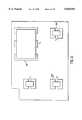
- FIG. 42shows a top and rear perspective view of a small form factor power supply for use with portable telephone equipment.
- FIG. 43shows a top and front perspective view of the small form factor power supply shown in FIG. 42.
- FIG. 44shows a bottom and front perspective view of the small form factor power supply shown in FIG. 42.
- FIG. 45shows a side perspective view of the small form factor power supply shown in FIGS. 42-44 connected to a cellular telephone battery and telephone.
- FIG. 46shows a top front perspective view of the small form factor power supply shown in FIGS. 42-44 connected to a cellular telephone battery and telephone.
- FIG. 47shows a top and front perspective view of a small form factor power supply adapter connector for use with portable telephone equipment.
- FIG. 48shows a top perspective view of the adapter connector shown in FIG. 47.
- FIG. 49shows a bottom perspective view of the adapter connector shown in FIG. 47
- FIG. 50shows a right side view of the adapter connector shown in FIG. 47.
- the inventionis embodied in an improved small form factor power supply.
- the small form factor power supplyis packaged in a small volume and produces over 75 watts of power with temperatures below 140° F.
- Preferred embodimentsare used to power portable computers.
- further embodiments of the inventionmay be used with other electronic devices, such as computer peripherals, audio and video electronics, portable telephone equipment and the like.
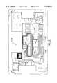
- FIG. 1shows a block diagram of the power supply according to the invention. All components on the left side of a magnetic core 20 are part of the primary portion 100 and all portions on the right hand side are part of the secondary portion 200 of the power supply.
- the primary portion 100includes a primary rectifier and input circuit 110, a first primary and drive circuit 120, a second primary and drive circuit 130, a primary feedback circuit 140 and a controller 150.
- the secondary portion 200includes a secondary output circuit 210 and a secondary feedback circuit 240.
- the function of the primary rectifier and input circuit 110is to couple the embodiment 10 to the line voltage (for example 110 volt, 60 Hz), to rectify that voltage and provide DC power for the remainder of the primary portion 100 and a ground path for the primary circuits 120 and 130.
- the controller 150which may be a Unitrode 3875 provides two square wave driver signals 152 and 154 having alterable phases to the first and the second primary circuits 120 and 130.
- the first and second primary circuitsare resonant circuits that are resonant at about the frequency of the driver signals and include coils that are coupled to the core 20, which may be a planar or low profile "E" type core, which may be any low loss material, as is shown in a sectional view in FIG. 2.
- the driver signalsare magnetically coupled to the core 20 by first and second primary coils contained within the circuits 120, 130.
- the coil 212 in the secondary circuit 210is preferably positioned relative to the coils of the two primary cores so that the coil in the secondary circuit is at a summing point of the magnetic flux from the primary circuit coils. If a planar or low profile "E" type core as shown in FIG. 2 is used, the coil 212 for the secondary circuit 210 is positioned about the central leg 22. The coil for the feedback circuits 140 is positioned on one of the outer legs 24, 26. As a result, the magnetic flux from the two primary coils of the primary circuits 120, 130 are summed at the position where the secondary coil 212 for the secondary circuit 210 is positioned. (This positioning of the coils is shown in FIG. 1 by using the double line to indicate the central leg 22 and a single line to represent the outer legs 24, 26).
- the amplitude of the DC voltage and current produced by the secondary circuit 210are monitored by the secondary feedback circuit 230.
- the primary feedback circuit 140 and the secondary feedback circuit 230are magnetically coupled by coils positioned on another core 23 to provide a feedback signal to the controller 150.
- the controlleralters the relative phase between the two driver signals 152 and 154 to obtain the desired magnitude of the voltage and current. Since the secondary coil 212 is located at a summing point on the core of the flux from the two primary coils, as the phase between the driving signals 152 and 154 to the two primary coils alters, the magnitude of the current and voltage induced in the secondary coil will vary. This will permit control of the secondary circuit 210 output voltage and current, thereby providing a readily controlled output voltage.
- FIG. 3shows a more detailed schematic of an embodiment of the invention.
- a standard AC plugmay be coupled to input nodes 111, 112 to a first filter coil L1 that is coupled to a full wave rectifier bridge 113, which may be a MDA106G.
- Filtering capacitors C1, C2, C7, C8are also coupled to the bridge 113 and one side of the bridge is coupled to AC ground.
- the other side of the bridgeis coupled to the primary coils 122 and 132 of the first and second primary circuits 120, 130 respectively.
- the other terminal of the primary coils 122, 132are coupled to the remainder of the primary circuits 120 and 130.
- Each of these primary circuits 120, 130also comprise a drive field effect 124, 134, which may be a MTP6N60 and a capacitor 126, 136.
- the coils 122, 132, transistors 124, 134 and capacitors 126, 136are selected so that the resonant frequency of the circuits 120, 130 is at about the frequency of the drive signals 152, 154 to maximize the efficiency of the power supply.
- the drive signal frequencyis about one megahertz, though other frequencies may be used.
- the drive signals 152 and 154are supplied by a controller 150 such as a Unitrode UC3875QP or other similar product.
- the controller 150receives the biasing power at pins 28 and 1 from the primary power supply circuit 160.
- Each of the coils 122 and 132induce a varying magnetic field in the outer legs of the core 20.
- the secondary coil 212which has a center tap 213, is coupled to a half wave rectifier bridge 214, which may comprise an MBRD660CT, and then is coupled to a filtering circuit 216 comprised of a capacitor 218, an inductor 220, and capacitors 222 and 224 to provide a DC regulated output 226.
- the regulationis provided by feeding back to the controller 150 a signal modulated by a current sensing amplifier circuit 232 and a voltage sensing circuit 240 comprising the feedback circuit 230.
- a further secondary carrier coil 242is coupled to one of the outer legs of the core 20.
- One of the legs of this transformer coil 242is coupled to an isolation feedback transformer T2.
- the current sensing circuittakes the output of the center tap of the secondary coil 212 and provides a voltage drop across resistor R9 that is provided to current sensing amplifier circuit 232.
- the output of the current sensing amplifier circuit 232is added to a voltage dropped across R13 and is provided to an amplifier 244 in the voltage sensing circuit 240.
- the other input in the voltage sensing circuitis a reference voltage developed by the zener reference diode 246 and also provided as a biasing level to the current sensing amplifier circuit 232.
- the output of the amplifier 244is provided to the base of bipolar transistor Q3, which may be a MMBT2907T, configured in a common base configuration, to amplitude modulate the current through the secondary side coil 246.
- the primary side coil 156 of feedback transformer T2is magnetically coupled to the secondary side coil of 246 and generates an amplitude modulated signal that is envelope detected and integrated to provide a feedback voltage at input 22 of the controller 150.
- the controller 150determines that the voltage has exceeded a predetermined limit, indicating that either the current or voltage at the output has increased beyond the predetermined maximum.
- the controller 150determines that the voltage has exceeded a predetermined limit, indicating that either the current or voltage at the output has increased beyond the predetermined maximum.
- the relative phase difference of driver signals 152 and 154is increased. If the amplitude at input 22 decreases below a predetermined threshold indicating that the voltage or the current is below the desired levels, the relative phase of signals 152 and 154 is decreased towards zero to increase the voltage or current. Due to the summing effect of the magnetic flux at secondary coil 212, a highly efficient control or regulation of the power supply circuit is obtained.
- each of the electrical components in FIG. 2, other than the transformermay be mounted using surface mount devices on a printed circuit board.
- each of the inductors and transformer coresare low profile or planar cores mounted through cutouts formed in the printed circuit board.
- the coils of the inductors and transformersare provided by wiring traces on the circuit board that wrap around the portion of the appropriate core penetrating the circuit board. As a result, an extremely compact form factor may be obtained.
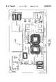
- FIG. 4shows a top planar view of such a printed circuit board with each inductor L1, L2 and transformer cores T1 and T2 identified.
- the assembled printed circuit boardmay be housed within a housing formed from an injection molded plastic dimensioned 2.75 ⁇ 4.5 ⁇ 0.436 inches without undue heating of the housing, although other dimensions may be used with a key to maintaining a thin profile of the power supply being the ratio of the surface area of the top and bottom surfaces to the overall thickness of the housing.
- a housingformed from an injection molded plastic dimensioned 2.75 ⁇ 4.5 ⁇ 0.436 inches without undue heating of the housing, although other dimensions may be used with a key to maintaining a thin profile of the power supply being the ratio of the surface area of the top and bottom surfaces to the overall thickness of the housing.
- proper heat sinksfor example, even smaller dimensions may be attained. For example, with such a housing, surface temperatures on the housing should not exceed one hundred twenty degrees Fahrenheit.
- a normal electrical plugsuch as a phased, three-prong plug, is coupled by an input cable (not shown) through a hole formed in the housing and an output cable (not shown) having a connector (not shown) coupled to the printed circuit board and to an output connector.
- the three-prong plugmay be formed within the housing with the prongs projecting from the housing to avoid the opening for a cable.
- the plugmay be of a pivotable type (not shown) mounted on the surface of the housing and rotate between a recessed position in a cutout formed within the housing and an in use position projecting at ninety degrees from the surface of the housing.
- regulated DC voltagefor example +5 or +16 volts DC
- additional secondary coils(not shown) with the appropriate number of windings to provide the voltage may be magnetically coupled to any of the legs of the transformer core 120.
- the appropriate circuitrymust then be provided for rectifying and filtering the output of this additional secondary coil.
- an additional regulated voltagemay be supplied by providing a feedback control circuit such as the type described above that provides the appropriate feedback.
- FIG. 5Ashows a top planar view of a case 300 for an additional embodiment of the invention substantially having the shape of a right parallelepiped.
- the casemay have dimensions of 5 inches long by 2.85 inches wide and the thickness (not shown) is 0.436 inches.
- Both the top portion of the case 300 and the bottom portion (not shown)define a number of louvers 304 defining multiple openings 302.
- the configuration of the openings 302 on both the top and bottom (not shown) portions of the coverare relatively unimportant.
- FIG. 5Bshows a partial cross-section of top portion of the case 300.
- a thin layer 306 of materialis connected to the bottom of the louvers 302 to cover the openings 304 that lead into the interior of the case 300.
- the thin layer 306is thin enough to still allow heat to pass through the openings 304 using ordinary convection.
- the thin layer 306is thick enough to prevent entry of liquids into the case 300, which could affect operation of the power supply.
- the thin layeris 1 to 3 mils thick.
- the thin layer 306is formed from a plastic material, such as Lexan, ABF or the like from which the remainder of the case is also formed.
- the thin film 306may be formed from metals, composites, ceramics or other heat conductive and liquid resistant materials.
- each heat sinkwhich comprises a thin sheet of thermally conductive material such as aluminum (which may be anodized) is configured preferably to fit precisely within the top or bottom portions of the case and defines a number of cutouts. These cutouts may provide clearance for certain components to be directly cooled by air entering through the openings 304 defined between the louvers 302 or may be provided for clearance of the components mounted on the printed circuit board (not shown).
- the patternshould be positioned so that when the unit is assembled, the heat sink material should provide adequate coverage over the openings in the case 300 to resist penetration of spilled liquids into the assembled unit. This allows the unit to comply with Underwriters Laboratories and other safety standards.
- the top and bottom heat sinksmay cover the entire power supply circuit board (not shown).
- other suitable materials besides aluminummay be used for the heat sinks.
- the undersides of the louversare scalloped (either along the length of the louver 302 or from side to side of the louver 302) to provide an air gap between the louvers 302 and the heat sink to minimize conduction of the heat from the heat sink to the material of the case 300 and louvers 302.
- the louvers 302are spaced close together to form the openings 304 so that the openings 304 have a relatively narrow width.
- the width and depth of the openings 304are chosen so that fingers cannot come into contact with either the thin layer 306 or the heat sinks under the thin layer 306. This minimizes the heat transfer to the user so that the touch temperature of the unit appears lower than the actual temperature.
- the openings 304are 3 to 5 mm, which is narrow enough to prevent the entry of fingers from small children.
- narrower or wider openings 304may be used, with the width being selected based upon the environment in which the power supply will be used.
- FIG. 5Cillustrates a partial cross-section of another embodiment of the louvers in accordance with an embodiment of the present invention.
- the louvers 310are formed from a single piece of material with raised ridges 312 separated by depressions 314.
- the depressionsare connected and secured to the heat sink 316 (such as those shown in FIG. 6) by adhesives, snap fit, simple contact or the like.
- the raised ridges 312 of the louvers 310are spaced close together to form the depressions 314 so that the depressions 314 have a relatively narrow width.
- the width and depth of the depressions 314are chosen so that fingers cannot come into contact with either the bottom of the depressions 314 or the heat sink 316.
- the depressions 314are 3 to 5 mm, which is narrow enough to prevent the entry of fingers from small children. However, in alternative embodiments, narrower or wider depressions 314 may be used, with the width being selected based upon the environment in which the power supply will be used.
- an air gap 318is formed beneath an undersurface 320 of the raised ridges 312 and the heat sink 316. The air gap 318 acts as an insulator so that the touch temperature of the case is lower than the actual temperature of the power supply heat sink 316.
- the raised ridges 312 and the depressions 314are formed from a plastic material, such as Lexan, ABF or the like from which the remainder of the case is also formed.
- the raised ridges 312 and the depressions 314may be formed from composites, ceramics or other heat conductive resistant and liquid resistant materials.
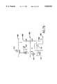
- FIGS. 7A and 7Bshow a schematic for the power supply circuit 800 with all resistance in ohms and all capacitance in microfarads unless otherwise labeled.
- the power supplyis formed on a multilayer printed circuit board (not shown) having length and width dimensions that are only slightly smaller than the exterior of the case and fit as precisely as possible within the chamber of the case 300 sandwiched between the heat sinks to minimize movement after assembly.
- surface mount devicesare used to minimize the vertical dimension and all coil cores are preferably planar, low profile cores. Optimally, parts having the smallest possible thickness should be used.
- the power supply 800includes an input circuit 810 that may be coupled to any AC power source preferably having a frequency of between about 50 to 90 hertz and preferably having a voltage of between about 90 to 240 Volts AC.
- This input circuit 810may include a full wave bridge rectifier 812, a filter circuit 814 and a regulation circuit 816 to provide an independent power supply for all integrated circuits used on the primary side 824 of the circuit.
- the input regulator circuit 816may also include a center tapped coil 819 mounted on one of the exterior legs of the "E" planar core 822 of the transformer 820. (Preferably, the planar "E" core of the type shown in FIG.
- a controller integrated circuit U1provides the four control signals for powering the MOSFETs coupled to the two primary coils 825 and 827 with their center taps coupled to Vbias.
- the outputs of integrated circuit U1 at pins 7 through 10provide the control signals to a MOSFET driver circuit U2 such that MOSFETs Q1, Q2, Q4 and Q5 provide the appropriate phase control as is described in connection with FIG. 8.
- Integrated circuit U2may be for example a 4468 available from Micrel, Teledyne and Telcom.
- Each of power switching MOSFET transistor pairs Q1 and Q2, and Q4 and Q5are coupled to center tapped primary coils 825 and 827, respectively.
- These transistorspreferably have heat sinks (not shown) coupled to their cases, and/or these heat sinks may also be thermally coupled to one of the heat sinks mounted immediately below and immediately above the top and bottom heat sinks for better thermal control.
- the capacitance of the MOSFETs Q1, Q2, Q4 and Q5 and the inductance of the coils 825 and 827are selected to provide resonance at the frequency at which the drive signals are supplied, which may be about 1 MHz. Nonetheless, other frequencies may be used, for example, between a range of about 500 KHz to 2 MHz.
- FIG. 8shows a timing diagram of the signals at nodes L through Q shown on FIG. 7A and 7B.
- the integrated circuit U1as described in more detail below, through feedback, provides MOSFET driving signals L through O.
- the MOSFET driving signals provided to each primary winding, 825 and 827i.e., L and M for primary winding 825 and N and O for primary winding 827) are always one hundred eighty degrees out of phase as shown in FIG. 8.
- the relative phase relationship of driving signal pair L and M for primary winding 825 with respect to driving signal N and O for primary winding 827may be changed by the integrated circuit controller U1 in the manner described below to provided the regulated DC output voltage at connectors 846 and 848.
- the resistors R10 through R13 and the capacitors C10 through C13combine with the integrated circuit U2 to provide preferably driving pulses L through O with a duty cycle of less than 50 percent. This ensures that the FETS in a pair (i.e., Q1 and Q2 for winding 825 and Q4 and Q5 for winding 827) are never both on at the same time to provide zero resonant switching and reduce power consumption.
- MOSFET pair Q1 and Q2are preferably never on the same time and MOSFET pair Q4 and Q5 are preferably never on at the same time.
- MOSFET Q1will turn on just about when the voltage at node P, which is at the drain of transistor Q1, reaches a minimum and will turn off immediately after the voltage at the drain of transistor Q1, goes above that minimum level.
- transistor Q2will only be on when the voltage at the drain is almost at the minimum.
- Transistor Q4will also only be on when the voltage at node Q is virtually at its minimum and the transistor Q5 will only be on when the voltage at its drain is nearly at its minimum.
- the duty cycle of signals L through Ois selected so that the waveforms P and Q are substantially trapezoidal with clipping occurring by transistors Q1, Q2, Q4 and Q5. This permits operation of the circuit over a wider range of input voltages.
- transistors Q1, Q2, Q4 and Q5need not clip so that the waveshapes at the drains of these transistors are substantially sinusoidal.
- a square wave on the drains of the actual transistorscould be used but would probably require larger cores.
- a single secondary winding 840is located at the magnetic summing node of the core 822 (i.e., the center leg of the low profile "E" type core shown in FIG. 2). That secondary winding 840 is coupled to a rectifier circuit 842 and then to an output filter 844 including a filter choke L2 to provide the regulated DC output at connectors 846, 848 in the manner described below.
- the center tap of the secondary winding 842is coupled through a coil in the filter coil L2 sharing a common core with the coil in the output filter 844. Through resistor R23, this center tap of winding 842 provides a current sense input to a summing amplifier U3A.
- a voltage sense of the output DC regulated voltage Voutis provided to an amplifier including amplifier U3C.
- the sensed voltage signal at the output of amplifier U3Cis provided to the summing amplifier U3A through amplifier circuit U3B to provide the feedback necessary for the desired regulation of the DC output.
- the output of the summing amplifier U3Ais provided through an emitter follower transistor Q7 to the center tap of the secondary side 826 of the feedback transformer 850.
- This transformeris magnetically isolated from the transformer 820.
- the signal at the center tap of transformer 850amplitude modulates a carrier signal provided by winding 852 provided on the same exterior leg of the core 822 as primary winding 827. Preferably also, this should be the opposite exterior leg of the core 822 on which coil 819 and winding 825 are mounted.
- the primary side 824 coil of transformer 850provides an amplitude modulated feedback signal that has an amplitude envelope.
- a diode detectorcomprised of diode CR5 and resistor R17 strip the carrier away, leaving the amplitude envelope as a feedback control signal to the VMOD input (pin 1 of U1) to provide the feedback useful for altering of the phase relationship between the drive signal pairs of signals L and M on the one hand, and signals N and O, on the other hand to regulate the DC power supply output at connectors 846, 848.
- amplifierscomprising U3B and U3D along with the current and voltage sense signals cause the integrated circuit U1 to control the phase relationship between the drive signal pairs L and M, on the one hand, and N and O, on the other hand, to provide a constant power supply until the output voltage drops below about ten volts. Then, due to the feedback signal at pin 1 of the controller U1, the integrated circuit controller U1 controls the relative phase relationship between the pair of drive signals L and M, on the one hand, and N and O, on the other hand, to provide a constant current source down to a minimal voltage, which is preferably less than about one volt.
- Vcc used by the amplifiers U3A through U3D in the integrated circuit U3 and the voltage regulator U4 to generate the +5 volts used in the control circuitis supplied by a rectifier circuit 854.
- the rectifier circuit 854is also coupled to secondary coil 852.
- FIG. 9shows a block diagram 900 of the controller integrated circuit U1.
- Pins 13, 14, and 15cooperate together along with external components R3, R4, R5 and R6 to set the operational frequency of the oscillator 902 to be preferably at 2 MHz, although other frequencies may be selected.
- An output of the oscillator 902is coupled to an internal capacitor 901 to provide a triangle signal labeled Ramp on FIGS. 10A and 10B while another output of the oscillator 902 is a 2 MHz square wave coupled to exclusive OR gate 904 and the clock input of a D flip flop 907.
- a Schmitt trigger comparator 906compares the feedback signal VMOD at pin 1 with the ramp signal as is shown in FIGS. 10A and 10B.
- FIG. 10A and 10BIn FIG.
- the VMOD signalwhich is the envelope of the feedback signal from the feedback transformer 850 is at the maximum level, while in FIG. 10B, the VMOD signal is somewhat less than the maximum.
- the comparator 906cooperates with the D flip flop 907, the exclusive OR gate 904, and the associated logic gates 908 to generate one shot control signals J and K.
- the one shot drive signals J and Kare controlled so that both one shot control signals go high at the same time.
- the timing of the one shot control signal Jis retarded and the timing of the one shot control signal K is advanced.
- These one shot control signals J and Kare provided to one shot circuits 920 and 930 within the controller circuit U1, which have dual outputs VA and VC and VB and VD respectively.
- the one shots 920 and 930trigger on the rising edge of signals J and K respectively, and the durations to the falling edge of the control signals J and K are irrelevant provided that they fall before the one shots need to be retriggered. Due to the inclusion of inverters 922 and 932, the output pair of signals VA and VC and VB and VD are approximately one hundred and eighty degrees out of phase.
- the external capacitor C7 and resistor R7are coupled to pins 5 and 4 of the controller U1 to control the duration of the output pulses at the one shot 920 and the one shot 930 to trigger them for the same duration. Further, these component values are selected to be as near as possible to provide a fifty percent duty cycle on the outputs L through O of the MOSFET driver circuit U2 at the frequency of operation.
- the controller circuit U1also includes a reference voltage generator 940 that provides the reference voltage for the over voltage protection circuit 942 and the comparator 944.
- a reference voltage generator 940that provides the reference voltage for the over voltage protection circuit 942 and the comparator 944.
- an over voltage protection circuit 830 having a coil 832is located at or near the summing node of the E block core 822.
- the value of the components within over voltage protection circuit 830are selected such that if the output voltage DC Output goes above a predetermined threshold, silicon controlled rectifier (SCR) Q3 will fire, shunting the Vbias to ground. This will cause the integrated circuits U1 and U2 to cease operating, thereby shutting down the output until the unit is recycled by temporarily removing the AC input voltage.
- SCRsilicon controlled rectifier
- a small, highly efficient form factor power supplyhas been disclosed that may be readily mounted within a small container having a thickness of 0.436 inches or less and having dimensions suitable for holding in a typical shirt pocket or calculator pocket in a brief case at high power levels of up to about 75 watts DC output with a surface temperature of about 140 degrees Fahrenheit at the surface. Thicknesses of less than 0.436 inches may be attainable if thinner electrolytic or other types of filtering capacitors can be obtained using standard production techniques. Alternatively, a thinner case may be obtained by maximizing coupling of heat generating components to the heat sinks with maximum air flow through the openings defined by the louvers 302 and by making the top and bottom surface areas of the case larger. Regulation of the output voltage may be readily attained.
- the secondary coilcan be positioned where the magnetic flux induced in the core from the two primary coils destructively interfere with each other and where the phase of the two driving signals is approximately one hundred eighty degrees out of phase at maximum output.
- cooling methodsother may be used, such as small electric fans, thermal-electric coolers or the like, to permit smaller form factor power supply configurations.
- the various resistors, capacitors, frequencies and inductorsmay be different and other types of integrated circuits may also be used.
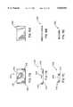
- FIGS. 12-16illustrate an improved transformer core 1010 in accordance with an embodiment of the present invention.
- FIG. 12Ashows a top plan view of the transformer core 1010, which is formed by a base plate 1012, a secondary leg 1014 and a pair of primary legs 1016 and 1018.
- the secondary leg 1014 and the primary legs of the transformer 1010may be bosses attached to the base plate 1012 by welds, magnetically permeable adhesives, or the like, or the entire assembly may be molded using magnetically permeable powder.
- FIG. 12B and 12Cshow two side plan views of how the transformer legs 1014, 1016, and 1018 are positioned on the base plate.
- FIGS. 13A and 13Cshow side plan views of the transformer cap 1020.
- the transformer core 1010 and transformer cap 1020are formed from a ferrite material.
- the operational frequency range of the coreis from about 0.5 to 1.0 MHz.
- the initial magnetic permeabilityis preferably 1400 ⁇ 20%.
- the saturation flux densitymay be 5300 gauss, and the Curie temperature may be 250 degrees Centigrade.
- the core loss while operating at a frequency of 1 MHzshould preferably be approximately 500 KW/m at 500 gauss. In other embodiments, different core parameters may be used.
- the base plate 1012 and the transformer capare dimensioned to be 1.260 ⁇ 1.260 ⁇ 0.075 inches.
- the secondary transformer leg 1014is dimensioned to be 0.800 ⁇ 0.200 by 0.060 inches, and each primary transformer leg is 0.133 ⁇ 0.700 ⁇ 0.060 inches.
- the secondary transformer leg 1014is positioned away from the primary transformer legs 1016 and 1018, as shown in FIGS. 12A-12C, to maximize the cross-sectional area of each of the transformer legs (i.e., the length and width of the transformer legs). This maximizes a ratio of the cross-sectional area of the transformer legs to the windings, thereby requiring less windings for the same magnetic coupling.
- the improved transformer corealso provides this maximized ratio while maintaining the ratio of the secondary to the primary windings at a constant value.
- slightly different dimensions for the core partsmay be used.
- the secondary coilis still positioned at a summing point of the primary coils.
- FIG. 14shows a printed circuit card layer 1030 without secondary or primary cores attached and having cutouts 1014', 1016' and 1018' to allow the corresponding transformer legs 1014, 1016 and 1018 to pass through the printed circuit board.
- FIG. 15shows another printed circuit card layer 1030" in which a secondary coil pattern 1040 surrounding the cut-out 1014' for the secondary transformer leg 1014.
- FIG. 16shows still another printed circuit card layer 1030' in which primary coil patterns 1042 and 1044 surround the cut-outs 1016' and 1018' for the to primary transformer legs 1016 and 1018, respectively.
- FIGS. 17-22illustrate an alternative embodiment using two transformer cores 1110 in accordance with the present invention.
- FIG. 17Ashows a top plan view of bottom portion of the transformer core 1110, which is formed by a base plate 1112, a central leg 1114 and a pair of peripheral legs 1116 and 1118.
- the central leg 1114 and the peripheral legs of the transformer 1110may be bosses attached to the base plate 1112 by welds, magnetically permeable adhesives, or the like, or the entire assembly may be molded using magnetically permeable powder.
- FIG. 17B and 17Cshow two side plan views of how the transformer legs 1114, 1116, and 1118 are positioned on the base plate 1112.
- FIG. 17Ashows a top plan view of bottom portion of the transformer core 1110, which is formed by a base plate 1112, a central leg 1114 and a pair of peripheral legs 1116 and 1118.
- the central leg 1114 and the peripheral legs of the transformer 1110may be bosses attached to the base plate 11
- FIGS. 18A and 18Cshow side plan views of the transformer cap 1120.
- the transformer core 1110 and transformer cap 1120are formed from a ferrite material that has properties and characteristics that are similar to those of the embodiment with the transformer core 1010, discussed-above.
- the base plate 1112 and the transformer cap 1120are dimensioned to be 1.113 ⁇ 1.113 ⁇ 0.075 inches.
- the central transformer leg 1114is dimensioned to be 0.300 ⁇ 0.300 by 0.060 inches, and each peripheral transformer leg is 0.075 ⁇ 0.630 ⁇ 0.060 inches.
- the central transformer leg 1114is positioned away from the peripheral transformer legs 1116 and 1118, as shown in FIGS. 17A-17C, to maximize the cross-sectional area of the central transformer leg 1114 (i.e., the length and width of the central transformer leg). This maximizes a ratio of the cross-sectional area of the central transformer leg 1114 to the windings, thereby requiring less windings for the same magnetic coupling.
- the improved transformer corealso provides this maximized ratio while maintaining the ratio of the secondary to the primary windings at a constant value. Also, as described in the previous transformer core 1010 embodiment, the secondary coil is still positioned at a summing point of the primary coils.
- FIG. 19shows a printed circuit card layer 1130A defining a secondary coil 1040' and having cutouts 1114', 1116' and 1118' and cutouts 1114", 1116" and 1118" to allow the corresponding transformer legs 1114, 1116 and 1118 of two transformer cores 1110 to pass through the printed circuit board.
- the secondary coil pattern 1140'passes around both central leg cutouts 1114' and 1114" to magnetically couple the secondary coil pattern 1040' with the summing point of two primary coils (see FIGS. 20 and 21).
- FIG. 20shows another layer 1330B of the printed circuit card in which two primary coil patterns 1142' and 1142" surround the corresponding central cutout 1114' and 1114", respectively.
- FIG. 21shows another printed circuit card layer 1130C in which two additional primary coil patterns 1144' and 1144" surround the corresponding central cutout 1114' and 1114", respectively. It should be noted that primary coil patterns 1144' and 1144" are coupled to corresponding primary coil patterns 1142' and 1142" to form the two primary coils that drive the secondary coil.
- FIG. 22shows still another printed circuit card layer 1130D in which a secondary coil pattern 1140" surrounds the corresponding central cut-out 1114' and 1114", respectively. It should be noted that secondary coil pattern 1140' is coupled to the corresponding secondary coil pattern 1140" to form the secondary coil that is coupled to the primary coils. Finally, it should be pointed out that the ancillary coil patterns 1146 surrounding the peripheral legs 1116' and 1116" are provided to produce a signal useful for protecting the circuit from over voltage.
- the small form factor power supplyis capable of supplying sufficient power to a personal computer or the like, even when the batteries are thoroughly discharged.
- the constant current at the output connectors 846, 848can provide minimal voltages down to about less than one volt because the controller U1 can attain relative phase shifts between the drive signal pairs to between about one degree to one hundred eighty degrees (i.e., signal N lags signal L between about one degree to one hundred eighty degrees and signal O and lags signal M between about one degree and one hundred eighty degrees).
- the slope of the output voltage curveis relatively constant until the output current reaches approximately 2.0 amperes, then slopes down to 10 volts at which time the output current is essentially constant at approximately 3.6 amperes for voltages under 10 volts.
- the output power curveincreases relatively linearly until the current level reaches approximately 2.2 amperes, at which time the output power curve tends to level off until the current reaches it maximum value of approximately 3.6 amperes. Therefore, the power supply is capable of providing constant current to the personal computer or the like, even if the battery is only capable of producing a fraction of a volt.
- This power curveis determined as a result of the selected amplifier configuration associated with integrated circuit U3, which may be an LM 324 on the secondary side 826.
- the predetermined limitmay be as high as 75 watts DC for a power supply having an upper and lower surface area within the case 300 of about 14 square inches and a thickness of about 0.436 inches or less so that the ratio of the top or bottom surface areas to the thickness is about 30:1.
- the circuitcan readily be programmed to provide other power/current characteristics, such as the power characteristics for lap top computers, appliances, cellular or portable telephones, notebook computers, game systems or the like. This may be accomplished by coupling additional resistors to ground and/or +5 volts (generated by a voltage regulator U4) to the current control and voltage control inputs.
- additional resistorsto ground and/or +5 volts (generated by a voltage regulator U4) to the current control and voltage control inputs.
- the current control input 860 and voltage control input 862can be coupled through a cable 882 to control circuits 884 commonly contained within the rechargeable batteries 886 coupled to the DC output connectors 846 and 848.
- control circuits 884may contain amplifiers 888, resistors 890, digital to analog converters or any other analog signal generator that may be coupled to the current and voltage control inputs 860, 862 through the cable 882 coupled to the battery terminals for charging. This would permit the controller in the battery programmatically to regulate the voltage and the current provided at the DC output to minimize recharging time based upon the known characteristics of the battery.
- the programing of the small form factor power supplyis carried out using either resistive programing or analog programing.
- other programing methodsmay be employed, such as digital or microprocessor controlled programing (with or without resistance ladder networks), with the type of programing technique being dependent on the power requirements of the device.
- FIG. 24is a schematic of a programing circuit in accordance with an embodiment of the present invention that is used to resistively program the power supply to produce between 0 and 16 volts
- FIG. 25is a schematic of another programing circuit in accordance with an embodiment of the present invention that is used to resistively program the power supply to produce between 16 and 18 volts
- FIG. 26is an end view of a connector that mates with the small form factor power supply (shown in FIGS. 3 and 7) and is useable to program the small form factor power supply, as shown in FIGS. 24 and 25.
- the power supplymay be programmed remotely to provide the required power at voltages between 0 to 18 volts using various external cables having built in resistances that program the power supply to output the required power level (i.e., voltage and current).
- This methodallows the small form factor power supply to be programmed for any value of voltage and/or current by connecting a resistor from the voltage and/or current programming pins (e.g., pins 1 and 4) to ground (e.g., pin 3) as shown in FIG. 24, or from the voltage programming pin (e.g., pin 1) to VOUT (e.g., pin 4) for voltages above 16 volts as shown in FIG. 25.
- V OUToutput voltage
- V OUToutput voltage
- analog programming of the small form factor power supplyis used. This method allows the small form factor power supply to be programmed for any value of voltage and/or current by providing an analog voltage signal from the respective programming pins and ground.
- V Pprogramming voltage applied to pin 4 with respect to pin 3;
- V OUToutput voltage
- the power supplymay interface with a programmable current generator interface, such as an MC33340 fast charge battery controller manufactured by Motorola, Inc. of Schaumberg, Ill. or a BQ2002C manufacture by Benchmarq, Dallas, Tex.
- a programmable current generator interfacesuch as an MC33340 fast charge battery controller manufactured by Motorola, Inc. of Schaumberg, Ill. or a BQ2002C manufacture by Benchmarq, Dallas, Tex.
- a programmable current generator interfacesuch as an MC33340 fast charge battery controller manufactured by Motorola, Inc. of Schaumberg, Ill. or a BQ2002C manufacture by Benchmarq, Dallas, Tex.
- the cableincludes a chip that is adapted to work with a specific device, such as a cellular telephone, laptop computer or the like, so that the charging characteristics of the power supply are altered as needed by simply changing cables.
- a generic cablecan be used and an adapter may be connected to the power supply between the cable and the power supply that contains different resistors that program the power supply to provide a desired power supply.
- an adaptermay be connected to the power supply between the cable and the power supply that contains different resistors that program the power supply to provide a desired power supply.
- precise charge terminationis difficult to detect when the battery reaches saturation.
- preferred embodiments of the present inventiondetect the knee of the power curve shown in FIG. 11 and reduce the current to deliver at a more steady rate.
- FIGS. 27(a)-34(c)show various cables with connectors in accordance with embodiments of the present invention that program the small form factor power supply for supplying power to different devices.
- These cableshave a connector 1500 for connecting with the small form factor power supply and use various configurations of resistances and wire connections to program the small form factor power supply to work with various devices.
- NCno connection
- GNDground (e.g., from pin 3 of FIG. 26).
- FIGS. 28(a)-28(c)show views of a cable 1502 having a connector 1504 for use with IBM computers, such as the "ThinkPad” or the like. No resistances are provided in the connectors 1500 and 1504, since the IBM computers provide their own power regulation, and the pins from the small form power supply (e.g., FIG. 27(c)) are converted to a compatible connector and pin out, as shown in FIG. 27(b).
- FIGS. 28(a)-28(c)show views of a cable 1506 having a connector 1508 for use with IBM computers, such as the "ThinkPad” or the like, and for Compaq computers, such as the Armada or the like.
- FIGS. 29(a)-29(c)show views of a cable 1510 having a connector 1512 for use with for Compaq computers, such as the Contura, LTE or the like, Toshiba computers, such as the Satellite and the Portege, Gateway computers, such as the Solo, and Hitachi computers, such as the C120T and the like.
- Either the connector 1500 or the connector 1512use resistances between pins 2 and 4 of the small form factor power supply to program the small form factor power supply.
- FIGS. 31(a)-30(b)show views of a cable 1514 that does not have a connector.
- the end 1516 of the cable 1514is left with bear wires to be configured to work with various computers that don't use the resistances or connectors shown in the other cables. Since the cable 1514 has no end connector, it can be wired to match various computer configurations.
- FIGS. 31(a)-31(c)show views of a cable 1518 having a connector 1520 for use with another configuration of a computer. Either the connector 1500 or the connector 1520 use resistances between pins 1, 3 and 4 of the small form factor power supply to program the small form factor power supply.
- FIGS. 32(a)-32(c)show views of a cable 1522 having a connector 1524 for use with Hewlett Packard computers, such as the Ominibook or the like. Either the connector 1500 or the connector 1524 use resistances between pins 3 and 4 of the small form factor power supply to program the small form factor power supply.
- FIGS. 33(a)-33(c)show views of a cable 1526 having a connector 1528 for use with Toshiba computers, such as the Tecra or the like. Either the connector 1500 or the connector 1528 use resistances (having a different value than those for cable 1522) between pins 3 and 4 of the small form factor power supply to program the small form factor power supply.
- 34(a)-34(c)show views of a cable 1530 having a connector 1532 that is designed to be a universal cable that accepts various connector ends that can mate with different device. No resistances are provided in the connectors 1500 and 1532, since the cable 1530 is converted to be compatible with various devices based on the connector adapters connected to the connector 1532.
- FIGS. 35(a)-40(c)show various connector adapters for use with the female connector 1532 of the cable 1530 shown above in FIGS. 34(a)-34(c).
- FIGS. 35(a)-35(c)show a connector adapter 1534 having a male connector 1536 for connecting with the connector 1532 and has an end connector 1538 that converts the generic cable 1530 of FIGS. 34(a)-34(c) to correspond to the cable 1502 shown in FIGS. 27(a)-27(c).
- FIGS. 36(a)-36(c)show a connector adapter 1540 having connectors 1536 and 1542 that convert the generic cable 1530 of FIGS. 34(a)-34(c) to correspond to the cable 1506 shown in FIGS.
- FIGS. 37(a)-37(c)show a connector 1544 having connectors 1536 and 1546 that convert the generic cable 1530 of FIGS. 34(a)-34(c) to correspond to the cable 1510 shown in FIGS. 29(a)-29(c).
- FIGS. 38(a)-38(c)show a connector adapter 1548 having connectors 1536 and 15505 that convert the generic cable 1530 of FIGS. 34(a)-34(c) to correspond to the cable 1518 shown in FIGS. 31(a)-31(c).
- FIGS. 39(a)-39(c)show a connector adapter 1552 having connectors 1536 and 1554 that convert the generic cable 1530 of FIGS.
- FIGS. 40(a)-40(c)show a connector adapter 1556 having connectors 1536 and 1558 that convert the generic cable 1530 of FIGS. 34(a)-34(c) to correspond to the cable 1526 shown in FIGS. 33(a)-33(c).
- FIGS. 41(a) and 41(b)illustrate a block diagram and a schematic of an interface for providing power to more than one device at a time.
- a small form factor power supply 2000is connected through a cable 2002 to an interface 2004 that supports more than one device at a time by the power supply.
- the interface 2004can support two or more devices, with the number of devices being dependent on the number of power output ports.
- the power to each deviceis controlled by cable connections to each device, such as the cables and connectors described above in FIGS. 27(a)-40(c).
- the interface 2004receives the cable 2002, which has a first voltage wire 2006 providing a first voltage V1 and a second voltage wire 2008 providing ground G.
- Additional devicesare connected to wires 2006 and 2008 through taps 2010 and 2012.
- Tap 2012if necessary, feeds into a voltage regulator to change the voltage to that desired by the device and outputs a second voltage on wire 2014 and ground on wire 2016.
- the additional regulatormay be provided in the cable used for each device.
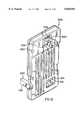
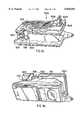
- FIGS. 42-44show various perspective views of a small form factor power supply 3000 that has been configured for use with portable telephone equipment in accordance with an embodiment of the present invention (note: these drawings are from 3-Dimensional CAD drawings and the many lines in the drawings indicate curves on the small form factor power supply and do not represent surface features).
- FIGS. 45 and 46show perspective views of the small form factor power supply 3000 connected to a cellular telephone battery and telephone.
- the small form factor power supply 3000is directed to charging portable telephone batteries. It has a housing 3002 similar to that described above and uses the charging circuitry described above. However, in alternative embodiments, different charging topologies may be used, depending on the charging environment, the battery type and the weight requirements of the small form factor power supply.
- Embodiments of the small form factor power supplycan be adapted to work with telephones manufactured by Audiovox, Ericsson/GE, Fujitsu, JRC, Mitsubishi/Daimondtel, Motorola, Murata, NEC, Nokia, Novatel, Oki, Panasonic, Sony, Uniden, AT&T, Tandy, Pioneer, JVC or the like.
- the small form factor power supplycan be used with a wide variety of portable telephone equipment, such as cordless telephones, cellular telephones, radio telephones, PCS telephones and the like.
- a power output 3010is adapted to fold out and includes a plurality of contacts 3012 that mate with the corresponding contacts (not shown) on a portable telephone equipment battery 3011.
- the contacts 3012 of the small form factor power supply 3000are placed in electrical contact with the contacts on the back of the battery 3011.
- the contacts 3012 of the small form factor power supplymay be placed in electrical contact with the contacts of the battery 3011 that provide power to the portable telephone equipment.
- the userpushes the power output 3010 through a port 3014 to force the power output 3010 to rotate down about a hinge 3016.
- the power output 3010may be spring loaded with a catch, detentes or other methods to lock the power output 3010 in the folded or unfolded position.
- the small form factor power supply 3000may use a recessed connector that connects to either the portable telephone equipment or battery using a cable such as described above and below.
- the small form factor power supply 3000also has support legs 3018 that include ends with guide tabs 3020.
- the guide tabs 3020are shaped to engage with channels 3021 on the portable telephone equipment battery 3011 to hold the battery 3011 in electrical contact with the small form factor power supply 3000 during charging.
- the support legs 3018are also capable of holding a portable telephone connected to the battery 3011, as shown in FIGS. 45 and 46.
- the support legs 3018are rotated out when the small form factor power supply 3000 is to be connected to a battery 3011.
- the userslides the battery 3011 to engage the channels 3021 of the battery 3011 with the guide tabs 3020 of the support legs 3018.
- each of the support legs 3018rotates independently of the other to simplify manufacturing and reduce complexity of the small form factor power supply 300.
- the support legs 3018may rotate out together as a unit and/or rotate out when the power output 3010 is rotated.
- the small form factor power supply 3000is capable of charging most telephone equipment batteries in less than 15 minutes. However, the actual charging time will vary based on the size of the battery and the battery chemistry. Most batteries (providing between 1 to 15 hours of high power operation) charge in 5-30 minutes.
- the small form factor power supply 3000includes a temperature sensor that is included in the small form factor power supply control chip to charge the battery as described above. This temperature sensor allows the small form factor power supply to determine the proper charging rate for a battery and avoid generating undue heat by overcharging or charging at too high a rate.
- the small form factor power supplycan be used to power the portable telephone equipment simultaneously with charging of an attached battery. Alternatively, the small form factor power supply may be able to power the portable telephone.
- the AC plug 3004, the power output 3010, and the support legs 3018are all designed to be folded in when the small form factor power supply 3000 is not in use. This minimizes the profile of the small form factor power supply when it is not in use and makes it easier to transport.
- the AC plug, the power output and the support legsmay be formed or maintained in the unfolded position, where the smaller profile is not needed or an advantage.
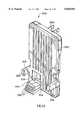
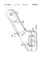
- FIG. 47-50show a perspective and plan views of a small form factor power supply adapter connector 4000 for use with portable telephone equipment in accordance with embodiments of the present invention (note: these drawings are from 3-Dimensional CAD drawings and the many lines in the drawings indicate curves on the small form factor power supply and do not represent surface features).
- the adapter connector 4000has a housing 4001 that includes a connector 4002 configured to mate with the connector 1532 of cable 1530 shown in FIGS. 34(a)-34(c). This adapter connector provides an upgrade path for users that already posses a small form factor power supply, as described above.
- the adapter connector 4000includes a plurality of contacts 4006 for connecting with corresponding contacts (not shown) on a portable telephone equipment battery.
- the housing 4001may also contain additional circuitry or electronics needed to properly program a small form factor power supply to charge a portable telephone equipment battery.
- the adapter connector 4000includes leg supports 4008 with guide tabs 4010 that engage with channels on a battery (similar to those shown in FIGS. 45 and 46 above).
- an end clip(not shown) attached to the adapter connector 4000 by elastic straps (not shown), or the like.
- the elastic strapsare threaded through eyelets 4011 so that the adapter connector 4000 can not slip off the battery.
- the leg supports 4008are foldable about a hinge 4012 to reduce the profile of the adapter connector 4000 when not in use and/or when being transported.
- the support legs 4008may be formed in a fixed open position.
- the small form factor power supplies described aboveare capable of charging various different types of batteries, such as NiCad and NiH.
- the small form factor power suppliesmay charge batteries using Zinc air, Lead acid, alkaline or the like.
- the power supplymay also be used to charge Lithium ion batteries, although a different control chip or circuitry may be required to handle the unique charging requirements of these batteries.
Landscapes
- Engineering & Computer Science (AREA)
- Power Engineering (AREA)
- Microelectronics & Electronic Packaging (AREA)
- Dc-Dc Converters (AREA)
Abstract
Description
Claims (36)
Priority Applications (20)
| Application Number | Priority Date | Filing Date | Title |
|---|---|---|---|
| US08/994,905US5838554A (en) | 1994-04-26 | 1997-12-19 | Small form factor power supply |
| US09/148,811US6091611A (en) | 1994-04-26 | 1998-09-04 | Connectors adapted for controlling a small form factor power supply |
| US09/213,018US5949213A (en) | 1994-04-26 | 1998-12-16 | Method and system for charging rechargeable batteries |
| US09/310,461US6172884B1 (en) | 1994-04-26 | 1999-05-12 | Small form factor power supply for powering electronics appliances |
| US09/541,826US6266261B1 (en) | 1994-04-26 | 2000-04-03 | DC power adapter system |
| US10/140,513US6693413B1 (en) | 1994-04-26 | 2002-05-07 | Programmable power supply |
| US10/277,116US6707284B2 (en) | 1994-04-26 | 2002-10-21 | Programmable power supply |
| US10/313,793US6809943B2 (en) | 1994-04-26 | 2002-12-05 | Programmable power supply |
| US10/314,004US6831848B2 (en) | 1994-04-26 | 2002-12-06 | Programmable power supply to simultaneously power a plurality of electronic devices |
| US10/927,566US6922347B2 (en) | 1994-04-26 | 2004-08-26 | Programmable power supply |
| US11/154,199US7145787B2 (en) | 1994-04-26 | 2005-06-16 | Programmable power supply |
| US11/403,046US7460381B2 (en) | 1994-04-26 | 2006-04-12 | Programmable power supply |
| US11/443,941US7266003B2 (en) | 1994-04-26 | 2006-05-31 | Programmable power supply |
| US11/448,318US20060227580A1 (en) | 1994-04-26 | 2006-06-07 | Programmable power supply |
| US11/481,387US7450390B2 (en) | 1994-04-26 | 2006-07-05 | Programmable power supply |
| US11/484,948US7649279B2 (en) | 1994-04-26 | 2006-07-12 | Power supply for simultaneously providing operating voltages to a plurality of devices |
| US11/891,187US7450403B2 (en) | 1994-04-26 | 2007-08-09 | Switching power supply utilizing switch-selectable resistors to determine output voltage |
| US11/891,233US7495941B2 (en) | 1994-04-26 | 2007-08-09 | Power supply equipment with matching indicators on converter and connector adapters |
| US12/074,212US7613021B2 (en) | 1994-04-26 | 2008-02-29 | Small form factor power supply |
| US12/592,530US7863770B2 (en) | 1994-04-26 | 2009-11-25 | Power supply equipment for simultaneously providing operating voltages to a plurality of devices |
Applications Claiming Priority (5)
| Application Number | Priority Date | Filing Date | Title |
|---|---|---|---|
| US08/233,121US5479331A (en) | 1994-04-26 | 1994-04-26 | Small form factor power supply |
| US248895P | 1995-08-17 | 1995-08-17 | |
| US08/567,369US5636110A (en) | 1994-04-26 | 1995-12-04 | Small form factor power supply |
| US76730796A | 1996-12-16 | 1996-12-16 | |
| US08/994,905US5838554A (en) | 1994-04-26 | 1997-12-19 | Small form factor power supply |
Related Parent Applications (1)
| Application Number | Title | Priority Date | Filing Date |
|---|---|---|---|
| US76730796AContinuation-In-Part | 1994-04-26 | 1996-12-16 |
Related Child Applications (3)
| Application Number | Title | Priority Date | Filing Date |
|---|---|---|---|
| US09/148,811Continuation-In-PartUS6091611A (en) | 1994-04-26 | 1998-09-04 | Connectors adapted for controlling a small form factor power supply |
| US09/148,811ContinuationUS6091611A (en) | 1994-04-26 | 1998-09-04 | Connectors adapted for controlling a small form factor power supply |
| US09/213,018Continuation-In-PartUS5949213A (en) | 1994-04-26 | 1998-12-16 | Method and system for charging rechargeable batteries |
Publications (1)
| Publication Number | Publication Date |
|---|---|
| US5838554Atrue US5838554A (en) | 1998-11-17 |
Family
ID=27485178
Family Applications (1)
| Application Number | Title | Priority Date | Filing Date |
|---|---|---|---|
| US08/994,905Expired - LifetimeUS5838554A (en) | 1994-04-26 | 1997-12-19 | Small form factor power supply |
Country Status (1)
| Country | Link |
|---|---|
| US (1) | US5838554A (en) |
Cited By (91)
| Publication number | Priority date | Publication date | Assignee | Title |
|---|---|---|---|---|
| US6091611A (en)* | 1994-04-26 | 2000-07-18 | Comarco Wireless Technologies, Inc. | Connectors adapted for controlling a small form factor power supply |
| US6191553B1 (en)* | 1998-08-25 | 2001-02-20 | Tu Feng-Jung | Portable charger with a separate base and mount with a belt clip attachment |
| US6462975B1 (en)* | 2001-05-23 | 2002-10-08 | Hon Hai Precisionind. Co., Ltd. | Foldable transformer |
| US6489591B1 (en)* | 2000-04-10 | 2002-12-03 | Illinois Tool Works Inc. | Cooling air circuits for welding machine |
| US6643158B2 (en) | 2001-10-31 | 2003-11-04 | Mobility Electronics, Inc. | Dual input AC/DC to programmable DC output converter |
| US6650560B2 (en) | 2001-12-03 | 2003-11-18 | Mobility Electronics, Inc. | Dual input AC and DC power supply having a programmable DC output utilizing single-loop optical feedback |
| US6662642B2 (en) | 2000-09-08 | 2003-12-16 | Automotive Technologies International, Inc. | Vehicle wireless sensing and communication system |
| US6680601B2 (en) | 2002-05-31 | 2004-01-20 | Telespree Communications | Circuit and method for power mediation in electronic device |
| US6693413B1 (en) | 1994-04-26 | 2004-02-17 | Comarco Wireless Technologies, Inc. | Programmable power supply |
| US6700808B2 (en) | 2002-02-08 | 2004-03-02 | Mobility Electronics, Inc. | Dual input AC and DC power supply having a programmable DC output utilizing a secondary buck converter |
| US20040085793A1 (en)* | 2001-12-03 | 2004-05-06 | Ejaz Afzal | Programmable power converter |
| US6751109B2 (en) | 2001-10-31 | 2004-06-15 | Mobility Electronics, Inc. | Dual input AC/DC/ battery operated power supply |
| US6791853B2 (en) | 2001-12-03 | 2004-09-14 | Mobility Electronics, Inc. | Dual input AC/DC power converter having a programmable peripheral power hub module |
| US6831848B2 (en) | 1994-04-26 | 2004-12-14 | Comarco Wireless Technologies, Inc. | Programmable power supply to simultaneously power a plurality of electronic devices |
| US6836101B2 (en) | 2002-12-05 | 2004-12-28 | Comarco Wireless Technologies, Inc. | Tip having active circuitry |
| EP1372254A3 (en)* | 2002-06-10 | 2005-05-25 | Comarco Wireless Technologies, Inc. | Programmable power supply capable of receiving AC and DC power input |
| US20050266730A1 (en)* | 1994-04-26 | 2005-12-01 | Comarco Wireless Technologies, Inc. | Programmable power supply |
| US20060076124A1 (en)* | 2004-09-07 | 2006-04-13 | Bahman Sharifipour | Apparatus for and method of cooling molded electronic circuits |
| US20060098358A1 (en)* | 2004-11-08 | 2006-05-11 | Wambsganss Peter M | Power supply configured to detect a power source |
| US20060098371A1 (en)* | 2004-11-08 | 2006-05-11 | Wambsganss Peter M | Temperature sensor for power supply |
| US20060098369A1 (en)* | 2004-11-08 | 2006-05-11 | Wambsganss Peter M | Microcontroller controlled power supply |
| US20060099858A1 (en)* | 2004-11-08 | 2006-05-11 | Wambsganss Peter M | Power supply connector |
| EP1521353A3 (en)* | 2003-06-20 | 2006-08-02 | Comarco Wireless Technologies, Inc. | Programmable AC/DC power supply |
| US20070159795A1 (en)* | 2006-01-12 | 2007-07-12 | Jui-Kai Tseng | Linear power supply |
| US20070190848A1 (en)* | 2006-02-02 | 2007-08-16 | Xiaoyang Zhang | Power adaptor and storage unit for portable devices |
| US20070297142A1 (en)* | 2006-06-21 | 2007-12-27 | Delta Electronics, Inc. | Power supply apparatus having passive heat-dissipation mechanism and fabrication method thereof |
| US20080048499A1 (en)* | 2004-06-18 | 2008-02-28 | Roman Litovsky | Controlling a Power Converter |
| US20090108681A1 (en)* | 2007-10-29 | 2009-04-30 | Bose Corporation | Automatic Power Source Configuration |
| US20090110214A1 (en)* | 2007-10-30 | 2009-04-30 | Litovsky Roman N | Controlled charging and use of power source |
| US20090290384A1 (en)* | 2008-05-21 | 2009-11-26 | Flextronics, Ap, Llc | High power factor isolated buck-type power factor correction converter |
| US20090290385A1 (en)* | 2008-05-21 | 2009-11-26 | Flextronics Ap, Llc | Resonant power factor correction converter |
| US20090310384A1 (en)* | 2008-06-12 | 2009-12-17 | Bahman Sharifipour | AC-DC input adapter |
| US7642671B2 (en) | 2006-04-28 | 2010-01-05 | Acco Brands Usa Llc | Power supply system providing two output voltages |
| US7646107B2 (en) | 2004-09-30 | 2010-01-12 | Targus Group Internatnional, Inc. | Programmable power adaptor |
| US20100142230A1 (en)* | 2007-01-16 | 2010-06-10 | Schroeder Genannt Berghegger Ralf | Simplified primary triggering circuit for the switch in a switched-mode power supply |
| US20100289466A1 (en)* | 2009-05-15 | 2010-11-18 | Flextronics Ap, Llc | Closed loop negative feedback system with low frequency modulated gain |
| US20100315839A1 (en)* | 2009-05-07 | 2010-12-16 | Zaohong Yang | Energy recovery snubber circuit for power converters |
| US20100322441A1 (en)* | 2009-06-23 | 2010-12-23 | Flextronics Ap, Llc | Notebook power supply with integrated subwoofer |
| US20110025286A1 (en)* | 2007-10-17 | 2011-02-03 | Power Systems Technologies Gmbh | Control Circuit For a Primary Controlled Switched Mode Power Supply with Improved Accuracy of the Voltage Control and Primary Controlled Switched Mode Power Supply |
| US20110170325A1 (en)* | 2010-01-14 | 2011-07-14 | Flextronics Ap, Llc | Line switcher for power converters |
| US8213204B2 (en) | 2009-04-01 | 2012-07-03 | Comarco Wireless Technologies, Inc. | Modular power adapter |
| US20120178506A1 (en)* | 2011-01-12 | 2012-07-12 | Yeoshua Sorias | Detachably integrated battery charger for mobile cell phones and like devices |
| US8279646B1 (en) | 2007-12-14 | 2012-10-02 | Flextronics Ap, Llc | Coordinated power sequencing to limit inrush currents and ensure optimum filtering |
| US8354760B2 (en) | 2009-10-28 | 2013-01-15 | Comarco Wireless Technologies, Inc. | Power supply equipment to simultaneously power multiple electronic device |
| US8441810B2 (en) | 2010-11-09 | 2013-05-14 | Flextronics Ap, Llc | Cascade power system architecture |
| US8488340B2 (en) | 2010-08-27 | 2013-07-16 | Flextronics Ap, Llc | Power converter with boost-buck-buck configuration utilizing an intermediate power regulating circuit |
| US8520410B2 (en) | 2010-11-09 | 2013-08-27 | Flextronics Ap, Llc | Virtual parametric high side MOSFET driver |
| US8550827B1 (en) | 2012-07-25 | 2013-10-08 | Targus Group International, Inc. | Multi-sleeve power tips |
| US20130325323A1 (en) | 1998-10-22 | 2013-12-05 | American Vehicular Sciences | Vehicle software upgrade techniques |
| US8654553B1 (en) | 2013-03-15 | 2014-02-18 | Flextronics Ap, Llc | Adaptive digital control of power factor correction front end |
| US8743565B2 (en) | 2012-07-27 | 2014-06-03 | Flextronics Ap, Llc | High power converter architecture |
| US8821199B2 (en) | 2012-07-25 | 2014-09-02 | Targus Group International, Inc. | Multi-prong power tip adaptor |
| US8842450B2 (en) | 2011-04-12 | 2014-09-23 | Flextronics, Ap, Llc | Power converter using multiple phase-shifting quasi-resonant converters |
| US8964413B2 (en) | 2010-04-22 | 2015-02-24 | Flextronics Ap, Llc | Two stage resonant converter enabling soft-switching in an isolated stage |
| USD723457S1 (en) | 2012-01-11 | 2015-03-03 | Yeoshua Sorias | Phone charger |
| US9019726B2 (en) | 2012-07-13 | 2015-04-28 | Flextronics Ap, Llc | Power converters with quasi-zero power consumption |
| US9019724B2 (en) | 2012-07-27 | 2015-04-28 | Flextronics Ap, Llc | High power converter architecture |
| US9093911B2 (en) | 2013-03-15 | 2015-07-28 | Flextronics Ap, Llc | Switching mode power converter using coded signal control |
| US9092712B2 (en) | 2012-11-02 | 2015-07-28 | Flextronics Ap, Llc | Embedded high frequency RFID |
| US9118253B2 (en) | 2012-08-15 | 2015-08-25 | Flextronics Ap, Llc | Energy conversion architecture with secondary side control delivered across transformer element |
| WO2015126629A1 (en)* | 2014-02-19 | 2015-08-27 | General Electric Company | System and method for reducing partial discharge in high voltage planar transformers |
| US9130384B2 (en) | 2011-10-06 | 2015-09-08 | Prong, Inc. | Smart phone and/or consumer electronics device charger system |
| US9136769B2 (en) | 2012-10-10 | 2015-09-15 | Flextronics Ap, Llc | Load change detection for switched mode power supply with low no load power |
| US9171809B2 (en) | 2013-03-05 | 2015-10-27 | Flextronics Ap, Llc | Escape routes |
| US9182177B2 (en) | 2011-07-12 | 2015-11-10 | Flextronics Ap, Llc | Heat transfer system with integrated evaporator and condenser |
| US9184668B2 (en) | 2013-03-15 | 2015-11-10 | Flextronics Ap, Llc | Power management integrated circuit partitioning with dedicated primary side control winding |
| US9203292B2 (en) | 2012-06-11 | 2015-12-01 | Power Systems Technologies Ltd. | Electromagnetic interference emission suppressor |
| US9203293B2 (en) | 2012-06-11 | 2015-12-01 | Power Systems Technologies Ltd. | Method of suppressing electromagnetic interference emission |
| US9276460B2 (en) | 2012-05-25 | 2016-03-01 | Flextronics Ap, Llc | Power converter with noise immunity |
| US9287792B2 (en) | 2012-08-13 | 2016-03-15 | Flextronics Ap, Llc | Control method to reduce switching loss on MOSFET |
| US9323267B2 (en) | 2013-03-14 | 2016-04-26 | Flextronics Ap, Llc | Method and implementation for eliminating random pulse during power up of digital signal controller |
| US9366394B2 (en) | 2012-06-27 | 2016-06-14 | Flextronics Ap, Llc | Automotive LED headlight cooling system |
| US9397065B1 (en) | 2013-08-27 | 2016-07-19 | Flextronics Ap, Llc | Fixture design for pre-attachment package on package component assembly |
| US9413179B2 (en) | 2013-07-09 | 2016-08-09 | Yeoshua Sorias | Detachably integrated battery charger for mobile cell phones and like devices |
| US9443358B2 (en) | 1995-06-07 | 2016-09-13 | Automotive Vehicular Sciences LLC | Vehicle software upgrade techniques |
| US9494658B2 (en) | 2013-03-14 | 2016-11-15 | Flextronics Ap, Llc | Approach for generation of power failure warning signal to maximize useable hold-up time with AC/DC rectifiers |
| US9521754B1 (en) | 2013-08-19 | 2016-12-13 | Multek Technologies Limited | Embedded components in a substrate |
| US9565748B2 (en) | 2013-10-28 | 2017-02-07 | Flextronics Ap, Llc | Nano-copper solder for filling thermal vias |
| US9605860B2 (en) | 2012-11-02 | 2017-03-28 | Flextronics Ap, Llc | Energy saving-exhaust control and auto shut off system |
| US9621053B1 (en) | 2014-08-05 | 2017-04-11 | Flextronics Ap, Llc | Peak power control technique for primary side controller operation in continuous conduction mode |
| US9661738B1 (en) | 2014-09-03 | 2017-05-23 | Flextronics Ap, Llc | Embedded coins for HDI or SEQ laminations |
| US9660540B2 (en) | 2012-11-05 | 2017-05-23 | Flextronics Ap, Llc | Digital error signal comparator |
| US20170149347A1 (en)* | 2015-10-30 | 2017-05-25 | Core Technologies Llc | Small form factor power conversion system |
| US9668336B1 (en) | 2012-05-18 | 2017-05-30 | Flextronics Ap, Llc | Inlay PCB with embedded coin board |
| US9711990B2 (en) | 2013-03-15 | 2017-07-18 | Flextronics Ap, Llc | No load detection and slew rate compensation |
| US10064292B2 (en) | 2016-03-21 | 2018-08-28 | Multek Technologies Limited | Recessed cavity in printed circuit board protected by LPI |
| US10123603B1 (en) | 2015-03-27 | 2018-11-13 | Multek Technologies Limited | Diffuse fiber optic lighting for luggage |
| US10321560B2 (en) | 2015-11-12 | 2019-06-11 | Multek Technologies Limited | Dummy core plus plating resist restrict resin process and structure |
| US10645807B1 (en) | 2013-08-27 | 2020-05-05 | Flextronics Ap, Llc. | Component attach on metal woven mesh |
| US10712398B1 (en) | 2016-06-21 | 2020-07-14 | Multek Technologies Limited | Measuring complex PCB-based interconnects in a production environment |
| US10855086B2 (en) | 2004-01-15 | 2020-12-01 | Comarco Wireless Systems Llc | Power supply equipment utilizing interchangeable tips to provide power and a data signal to electronic devices |
Citations (13)
| Publication number | Priority date | Publication date | Assignee | Title |
|---|---|---|---|---|
| US4257080A (en)* | 1978-06-13 | 1981-03-17 | Bartram Trevor C | Current limiting devices |
| US4307441A (en)* | 1980-07-28 | 1981-12-22 | United Technologies Corporation | Current balanced DC-to-DC converter |
| US4622627A (en)* | 1984-02-16 | 1986-11-11 | Theta-J Corporation | Switching electrical power supply utilizing miniature inductors integrally in a PCB |
| US4734839A (en)* | 1987-03-23 | 1988-03-29 | Barthold Fred O | Source volt-ampere/load volt-ampere differential converter |
| US4885674A (en)* | 1988-03-28 | 1989-12-05 | Varga Ljubomir D | Synthesis of load-independent switch-mode power converters |
| US4890214A (en)* | 1985-11-15 | 1989-12-26 | Nec Corporation | Start circuit for adapting a constant current generator to a wide variety of loads |
| US5019954A (en)* | 1989-06-23 | 1991-05-28 | Allied-Signal Inc. | AC/DC conversion with reduced supply waveform distortion |
| US5146394A (en)* | 1989-06-23 | 1992-09-08 | Matsushita Electric Industrial Co., Ltd. | Fly back converter switching power supply device |
| US5177675A (en)* | 1991-10-16 | 1993-01-05 | Shindengen Archer Corp. | Zero voltage, zero current, resonant converter |
| US5184291A (en)* | 1991-06-13 | 1993-02-02 | Crowe Lawrence E | Converter and inverter support module |
| US5309348A (en)* | 1992-08-13 | 1994-05-03 | Acer Peripherals, Inc. | Method and apparatus for preventing improper switching of a dual power supply |
| US5479331A (en)* | 1994-04-26 | 1995-12-26 | Comarco Wireless Technologies, Inc. | Small form factor power supply |
| US5636110A (en)* | 1994-04-26 | 1997-06-03 | Comarco Wireless Technologies, Inc. | Small form factor power supply |
- 1997
- 1997-12-19USUS08/994,905patent/US5838554A/ennot_activeExpired - Lifetime
Patent Citations (13)
| Publication number | Priority date | Publication date | Assignee | Title |
|---|---|---|---|---|
| US4257080A (en)* | 1978-06-13 | 1981-03-17 | Bartram Trevor C | Current limiting devices |
| US4307441A (en)* | 1980-07-28 | 1981-12-22 | United Technologies Corporation | Current balanced DC-to-DC converter |
| US4622627A (en)* | 1984-02-16 | 1986-11-11 | Theta-J Corporation | Switching electrical power supply utilizing miniature inductors integrally in a PCB |
| US4890214A (en)* | 1985-11-15 | 1989-12-26 | Nec Corporation | Start circuit for adapting a constant current generator to a wide variety of loads |
| US4734839A (en)* | 1987-03-23 | 1988-03-29 | Barthold Fred O | Source volt-ampere/load volt-ampere differential converter |
| US4885674A (en)* | 1988-03-28 | 1989-12-05 | Varga Ljubomir D | Synthesis of load-independent switch-mode power converters |
| US5019954A (en)* | 1989-06-23 | 1991-05-28 | Allied-Signal Inc. | AC/DC conversion with reduced supply waveform distortion |
| US5146394A (en)* | 1989-06-23 | 1992-09-08 | Matsushita Electric Industrial Co., Ltd. | Fly back converter switching power supply device |
| US5184291A (en)* | 1991-06-13 | 1993-02-02 | Crowe Lawrence E | Converter and inverter support module |
| US5177675A (en)* | 1991-10-16 | 1993-01-05 | Shindengen Archer Corp. | Zero voltage, zero current, resonant converter |
| US5309348A (en)* | 1992-08-13 | 1994-05-03 | Acer Peripherals, Inc. | Method and apparatus for preventing improper switching of a dual power supply |
| US5479331A (en)* | 1994-04-26 | 1995-12-26 | Comarco Wireless Technologies, Inc. | Small form factor power supply |
| US5636110A (en)* | 1994-04-26 | 1997-06-03 | Comarco Wireless Technologies, Inc. | Small form factor power supply |
Cited By (156)
| Publication number | Priority date | Publication date | Assignee | Title |
|---|---|---|---|---|
| US20060256595A1 (en)* | 1994-04-26 | 2006-11-16 | Comarco Wireless Technologies, Inc. | Power supply for simultaneously providing operating voltages to a plurality of devices |
| US20060215381A1 (en)* | 1994-04-26 | 2006-09-28 | Comarco Wireless Technologies, Inc. | Programmable power supply |
| US20100109436A1 (en)* | 1994-04-26 | 2010-05-06 | Comarco Wireless Technologies, Inc. | Power supply equipment for simultaneously providing operating voltages to a plurality of devices |
| US7863770B2 (en) | 1994-04-26 | 2011-01-04 | Comarco Wireless Technologies, Inc. | Power supply equipment for simultaneously providing operating voltages to a plurality of devices |
| US20070279952A1 (en)* | 1994-04-26 | 2007-12-06 | Comarco Wireless Technologies, Inc. | Switching power supply utilizing switch-selectable resistors to determine output voltage |
| US7266003B2 (en) | 1994-04-26 | 2007-09-04 | Comarco Wireless Technologies, Inc. | Programmable power supply |
| US7649279B2 (en) | 1994-04-26 | 2010-01-19 | Comarco Wireless Technologies, Inc | Power supply for simultaneously providing operating voltages to a plurality of devices |
| US7450403B2 (en) | 1994-04-26 | 2008-11-11 | Comarco Wireless Technologies, Inc. | Switching power supply utilizing switch-selectable resistors to determine output voltage |
| US6693413B1 (en) | 1994-04-26 | 2004-02-17 | Comarco Wireless Technologies, Inc. | Programmable power supply |
| US7450390B2 (en) | 1994-04-26 | 2008-11-11 | Comarco Wireless Technologies, Inc. | Programmable power supply |
| US7460381B2 (en) | 1994-04-26 | 2008-12-02 | Comarco Wireless Technologies, Inc. | Programmable power supply |
| US6707284B2 (en) | 1994-04-26 | 2004-03-16 | Comarco Wireless Technologies, Inc. | Programmable power supply |
| US7495941B2 (en) | 1994-04-26 | 2009-02-24 | Comarco Wireless Technologies, Inc. | Power supply equipment with matching indicators on converter and connector adapters |
| US7145787B2 (en) | 1994-04-26 | 2006-12-05 | Comarco Wireless Technologies, Inc. | Programmable power supply |
| US20050266730A1 (en)* | 1994-04-26 | 2005-12-01 | Comarco Wireless Technologies, Inc. | Programmable power supply |
| US6922347B2 (en) | 1994-04-26 | 2005-07-26 | Comarco Wireless Technologies, Inc. | Programmable power supply |
| US7613021B2 (en) | 1994-04-26 | 2009-11-03 | Comarco Wireless Technologies, Inc | Small form factor power supply |
| US6809943B2 (en) | 1994-04-26 | 2004-10-26 | Comarco Wireless Technologies, Inc. | Programmable power supply |
| US6831848B2 (en) | 1994-04-26 | 2004-12-14 | Comarco Wireless Technologies, Inc. | Programmable power supply to simultaneously power a plurality of electronic devices |
| US6091611A (en)* | 1994-04-26 | 2000-07-18 | Comarco Wireless Technologies, Inc. | Connectors adapted for controlling a small form factor power supply |
| US20060227580A1 (en)* | 1994-04-26 | 2006-10-12 | Comarco Wireless Technologies Inc. | Programmable power supply |
| US20050024907A1 (en)* | 1994-04-26 | 2005-02-03 | Comarco Wireless Technologies, Inc. | Programmable power supply |
| US20080151581A1 (en)* | 1994-04-26 | 2008-06-26 | Comarco Wireless Technologies, Inc. | Small form factor power supply |
| US9443358B2 (en) | 1995-06-07 | 2016-09-13 | Automotive Vehicular Sciences LLC | Vehicle software upgrade techniques |
| US6191553B1 (en)* | 1998-08-25 | 2001-02-20 | Tu Feng-Jung | Portable charger with a separate base and mount with a belt clip attachment |
| US10240935B2 (en) | 1998-10-22 | 2019-03-26 | American Vehicular Sciences Llc | Vehicle software upgrade techniques |
| US20130325323A1 (en) | 1998-10-22 | 2013-12-05 | American Vehicular Sciences | Vehicle software upgrade techniques |
| US6489591B1 (en)* | 2000-04-10 | 2002-12-03 | Illinois Tool Works Inc. | Cooling air circuits for welding machine |
| US6662642B2 (en) | 2000-09-08 | 2003-12-16 | Automotive Technologies International, Inc. | Vehicle wireless sensing and communication system |
| US6462975B1 (en)* | 2001-05-23 | 2002-10-08 | Hon Hai Precisionind. Co., Ltd. | Foldable transformer |
| US7646620B2 (en) | 2001-10-31 | 2010-01-12 | Igo, Inc. | AC/DC power converter |
| US20040037102A1 (en)* | 2001-10-31 | 2004-02-26 | Mobility Electronics Inc. | Dual input AC/DC to programmable DC output converter |
| US20060007715A1 (en)* | 2001-10-31 | 2006-01-12 | Mobility Electronics Inc. | AC/DC power converter |
| US6643158B2 (en) | 2001-10-31 | 2003-11-04 | Mobility Electronics, Inc. | Dual input AC/DC to programmable DC output converter |
| US20040170039A1 (en)* | 2001-10-31 | 2004-09-02 | Mobility Electronics Inc. | Dual input AC and DC power supply having a programmable DC output utilizing a secondary buck converter |
| US6775163B2 (en) | 2001-10-31 | 2004-08-10 | Mobility Electronics Inc. | Dual input AC/DC to programmable DC output converter |
| US6751109B2 (en) | 2001-10-31 | 2004-06-15 | Mobility Electronics, Inc. | Dual input AC/DC/ battery operated power supply |
| US6903950B2 (en) | 2001-12-03 | 2005-06-07 | Mobility Electronics, Inc. | Programmable power converter |
| US6791853B2 (en) | 2001-12-03 | 2004-09-14 | Mobility Electronics, Inc. | Dual input AC/DC power converter having a programmable peripheral power hub module |
| US20040085793A1 (en)* | 2001-12-03 | 2004-05-06 | Ejaz Afzal | Programmable power converter |
| US6650560B2 (en) | 2001-12-03 | 2003-11-18 | Mobility Electronics, Inc. | Dual input AC and DC power supply having a programmable DC output utilizing single-loop optical feedback |
| US6700808B2 (en) | 2002-02-08 | 2004-03-02 | Mobility Electronics, Inc. | Dual input AC and DC power supply having a programmable DC output utilizing a secondary buck converter |
| US6680601B2 (en) | 2002-05-31 | 2004-01-20 | Telespree Communications | Circuit and method for power mediation in electronic device |
| US7035126B1 (en) | 2002-06-10 | 2006-04-25 | Comarco Wireless Technologies, Inc. | Programmable power supply capable of receiving AC and DC power input |
| EP1372254A3 (en)* | 2002-06-10 | 2005-05-25 | Comarco Wireless Technologies, Inc. | Programmable power supply capable of receiving AC and DC power input |
| US20070182388A1 (en)* | 2002-12-05 | 2007-08-09 | Comarco Wireless Technologies, Inc. | Tip having active circuitry |
| US7365524B2 (en) | 2002-12-05 | 2008-04-29 | Comarco Wireless Technologies, Inc. | Tip having active circuitry |
| US20050024030A1 (en)* | 2002-12-05 | 2005-02-03 | Lanni Thomas W. | Tip having active circuitry |
| US6836101B2 (en) | 2002-12-05 | 2004-12-28 | Comarco Wireless Technologies, Inc. | Tip having active circuitry |
| US7193398B2 (en) | 2002-12-05 | 2007-03-20 | Comarco Wireless Technologies, Inc | Tip having active circuitry |
| EP1521353A3 (en)* | 2003-06-20 | 2006-08-02 | Comarco Wireless Technologies, Inc. | Programmable AC/DC power supply |
| US10855086B2 (en) | 2004-01-15 | 2020-12-01 | Comarco Wireless Systems Llc | Power supply equipment utilizing interchangeable tips to provide power and a data signal to electronic devices |
| US10855087B1 (en) | 2004-01-15 | 2020-12-01 | Comarco Wireless Systems Llc | Power supply systems |
| US10951042B2 (en) | 2004-01-15 | 2021-03-16 | Comarco Wireless Systems Llc | Power supply systems |
| US11586233B2 (en) | 2004-01-15 | 2023-02-21 | Comarco Wireless Systems Llc | Power supply systems |
| US7880330B2 (en) | 2004-06-18 | 2011-02-01 | Bose Corporation | Controlling a power converter |
| US20080048499A1 (en)* | 2004-06-18 | 2008-02-28 | Roman Litovsky | Controlling a Power Converter |
| US20060076124A1 (en)* | 2004-09-07 | 2006-04-13 | Bahman Sharifipour | Apparatus for and method of cooling molded electronic circuits |
| US8295048B2 (en) | 2004-09-07 | 2012-10-23 | Flextronics Ap, Llc | Apparatus for and method of cooling electronic circuits |
| US7885076B2 (en) | 2004-09-07 | 2011-02-08 | Flextronics Ap, Llc | Apparatus for and method of cooling molded electronic circuits |
| US20110103119A1 (en)* | 2004-09-07 | 2011-05-05 | Flextronics Ap, Llc | Apparatus for and method of cooling electronic circuits |
| US7646107B2 (en) | 2004-09-30 | 2010-01-12 | Targus Group Internatnional, Inc. | Programmable power adaptor |
| US20060098371A1 (en)* | 2004-11-08 | 2006-05-11 | Wambsganss Peter M | Temperature sensor for power supply |
| US20060099858A1 (en)* | 2004-11-08 | 2006-05-11 | Wambsganss Peter M | Power supply connector |
| US7108528B2 (en) | 2004-11-08 | 2006-09-19 | Rrc Power Solutions Gmbh | Power supply connector |
| US20060098369A1 (en)* | 2004-11-08 | 2006-05-11 | Wambsganss Peter M | Microcontroller controlled power supply |
| US7408132B2 (en) | 2004-11-08 | 2008-08-05 | Rrc Power Solutions Gmbh | Temperature sensor for power supply |
| US20060098358A1 (en)* | 2004-11-08 | 2006-05-11 | Wambsganss Peter M | Power supply configured to detect a power source |
| US20070159795A1 (en)* | 2006-01-12 | 2007-07-12 | Jui-Kai Tseng | Linear power supply |
| US7989981B2 (en) | 2006-02-02 | 2011-08-02 | Flextronics Ap, Llc | Power adaptor and storage unit for portable devices |
| US20070190848A1 (en)* | 2006-02-02 | 2007-08-16 | Xiaoyang Zhang | Power adaptor and storage unit for portable devices |
| US8212386B2 (en) | 2006-04-28 | 2012-07-03 | ACCO Brands Corporation | Power supply system |
| US7642671B2 (en) | 2006-04-28 | 2010-01-05 | Acco Brands Usa Llc | Power supply system providing two output voltages |
| EP2731226A2 (en) | 2006-04-28 | 2014-05-14 | ACCO Brands USA LLC | Power supply system |
| US20070297142A1 (en)* | 2006-06-21 | 2007-12-27 | Delta Electronics, Inc. | Power supply apparatus having passive heat-dissipation mechanism and fabrication method thereof |
| US8467201B2 (en) | 2007-01-16 | 2013-06-18 | Flextronics GmbH & Co KG | Simplified primary triggering circuit for the switch in a switched-mode power supply |
| US20100142230A1 (en)* | 2007-01-16 | 2010-06-10 | Schroeder Genannt Berghegger Ralf | Simplified primary triggering circuit for the switch in a switched-mode power supply |
| US8582323B2 (en) | 2007-10-17 | 2013-11-12 | Flextronics Ap, Llc | Control circuit for a primary controlled switched mode power supply with improved accuracy of the voltage control and primary controlled switched mode power supply |
| US20110025286A1 (en)* | 2007-10-17 | 2011-02-03 | Power Systems Technologies Gmbh | Control Circuit For a Primary Controlled Switched Mode Power Supply with Improved Accuracy of the Voltage Control and Primary Controlled Switched Mode Power Supply |
| US7656061B2 (en) | 2007-10-29 | 2010-02-02 | Bose Corporation | Automatic power source configuration |
| US20090108681A1 (en)* | 2007-10-29 | 2009-04-30 | Bose Corporation | Automatic Power Source Configuration |
| US7888907B2 (en) | 2007-10-30 | 2011-02-15 | Bose Corporation | Controlled charging and use of power source |
| US20090110214A1 (en)* | 2007-10-30 | 2009-04-30 | Litovsky Roman N | Controlled charging and use of power source |
| US8279646B1 (en) | 2007-12-14 | 2012-10-02 | Flextronics Ap, Llc | Coordinated power sequencing to limit inrush currents and ensure optimum filtering |
| US8102678B2 (en) | 2008-05-21 | 2012-01-24 | Flextronics Ap, Llc | High power factor isolated buck-type power factor correction converter |
| US20090290384A1 (en)* | 2008-05-21 | 2009-11-26 | Flextronics, Ap, Llc | High power factor isolated buck-type power factor correction converter |
| US8693213B2 (en) | 2008-05-21 | 2014-04-08 | Flextronics Ap, Llc | Resonant power factor correction converter |
| US20090290385A1 (en)* | 2008-05-21 | 2009-11-26 | Flextronics Ap, Llc | Resonant power factor correction converter |
| US20090310384A1 (en)* | 2008-06-12 | 2009-12-17 | Bahman Sharifipour | AC-DC input adapter |
| US8531174B2 (en) | 2008-06-12 | 2013-09-10 | Flextronics Ap, Llc | AC-DC input adapter |
| US8213204B2 (en) | 2009-04-01 | 2012-07-03 | Comarco Wireless Technologies, Inc. | Modular power adapter |
| US20100315839A1 (en)* | 2009-05-07 | 2010-12-16 | Zaohong Yang | Energy recovery snubber circuit for power converters |
| US8787044B2 (en) | 2009-05-07 | 2014-07-22 | Flextronics Ap, Llc | Energy recovery snubber circuit for power converters |
| US8040117B2 (en) | 2009-05-15 | 2011-10-18 | Flextronics Ap, Llc | Closed loop negative feedback system with low frequency modulated gain |
| US20100289466A1 (en)* | 2009-05-15 | 2010-11-18 | Flextronics Ap, Llc | Closed loop negative feedback system with low frequency modulated gain |
| US20100322441A1 (en)* | 2009-06-23 | 2010-12-23 | Flextronics Ap, Llc | Notebook power supply with integrated subwoofer |
| US8891803B2 (en) | 2009-06-23 | 2014-11-18 | Flextronics Ap, Llc | Notebook power supply with integrated subwoofer |
| US8354760B2 (en) | 2009-10-28 | 2013-01-15 | Comarco Wireless Technologies, Inc. | Power supply equipment to simultaneously power multiple electronic device |
| US20110170325A1 (en)* | 2010-01-14 | 2011-07-14 | Flextronics Ap, Llc | Line switcher for power converters |
| US8289741B2 (en) | 2010-01-14 | 2012-10-16 | Flextronics Ap, Llc | Line switcher for power converters |
| US8964413B2 (en) | 2010-04-22 | 2015-02-24 | Flextronics Ap, Llc | Two stage resonant converter enabling soft-switching in an isolated stage |
| US8488340B2 (en) | 2010-08-27 | 2013-07-16 | Flextronics Ap, Llc | Power converter with boost-buck-buck configuration utilizing an intermediate power regulating circuit |
| US8520410B2 (en) | 2010-11-09 | 2013-08-27 | Flextronics Ap, Llc | Virtual parametric high side MOSFET driver |
| US8441810B2 (en) | 2010-11-09 | 2013-05-14 | Flextronics Ap, Llc | Cascade power system architecture |
| US9088670B2 (en) | 2011-01-12 | 2015-07-21 | Yeoshua Sorias | Detachably integrated battery charger for mobile cell phones and like devices |
| US20120178506A1 (en)* | 2011-01-12 | 2012-07-12 | Yeoshua Sorias | Detachably integrated battery charger for mobile cell phones and like devices |
| US8712482B2 (en) | 2011-01-12 | 2014-04-29 | Yeoshua Sorias | Detachably integrated battery charger for mobile cell phones and like devices |
| US8712486B2 (en)* | 2011-01-12 | 2014-04-29 | Yeoshua Sorias | Detachably integrated battery charger for mobile cell phones and like devices |
| WO2012097118A1 (en)* | 2011-01-12 | 2012-07-19 | Sorias Yeoshua | Detachably integrated battery charger for mobile cell phones and like devices |
| US8842450B2 (en) | 2011-04-12 | 2014-09-23 | Flextronics, Ap, Llc | Power converter using multiple phase-shifting quasi-resonant converters |
| US9182177B2 (en) | 2011-07-12 | 2015-11-10 | Flextronics Ap, Llc | Heat transfer system with integrated evaporator and condenser |
| US9130384B2 (en) | 2011-10-06 | 2015-09-08 | Prong, Inc. | Smart phone and/or consumer electronics device charger system |
| USD723457S1 (en) | 2012-01-11 | 2015-03-03 | Yeoshua Sorias | Phone charger |
| US9668336B1 (en) | 2012-05-18 | 2017-05-30 | Flextronics Ap, Llc | Inlay PCB with embedded coin board |
| US9276460B2 (en) | 2012-05-25 | 2016-03-01 | Flextronics Ap, Llc | Power converter with noise immunity |
| US9203293B2 (en) | 2012-06-11 | 2015-12-01 | Power Systems Technologies Ltd. | Method of suppressing electromagnetic interference emission |
| US9203292B2 (en) | 2012-06-11 | 2015-12-01 | Power Systems Technologies Ltd. | Electromagnetic interference emission suppressor |
| US9366394B2 (en) | 2012-06-27 | 2016-06-14 | Flextronics Ap, Llc | Automotive LED headlight cooling system |
| US9019726B2 (en) | 2012-07-13 | 2015-04-28 | Flextronics Ap, Llc | Power converters with quasi-zero power consumption |
| US8821199B2 (en) | 2012-07-25 | 2014-09-02 | Targus Group International, Inc. | Multi-prong power tip adaptor |
| US8550827B1 (en) | 2012-07-25 | 2013-10-08 | Targus Group International, Inc. | Multi-sleeve power tips |
| US9019724B2 (en) | 2012-07-27 | 2015-04-28 | Flextronics Ap, Llc | High power converter architecture |
| US8743565B2 (en) | 2012-07-27 | 2014-06-03 | Flextronics Ap, Llc | High power converter architecture |
| US9287792B2 (en) | 2012-08-13 | 2016-03-15 | Flextronics Ap, Llc | Control method to reduce switching loss on MOSFET |
| US9312775B2 (en) | 2012-08-15 | 2016-04-12 | Flextronics Ap, Llc | Reconstruction pulse shape integrity in feedback control environment |
| US9118253B2 (en) | 2012-08-15 | 2015-08-25 | Flextronics Ap, Llc | Energy conversion architecture with secondary side control delivered across transformer element |
| US9318965B2 (en) | 2012-10-10 | 2016-04-19 | Flextronics Ap, Llc | Method to control a minimum pulsewidth in a switch mode power supply |
| US9136769B2 (en) | 2012-10-10 | 2015-09-15 | Flextronics Ap, Llc | Load change detection for switched mode power supply with low no load power |
| US9605860B2 (en) | 2012-11-02 | 2017-03-28 | Flextronics Ap, Llc | Energy saving-exhaust control and auto shut off system |
| US9092712B2 (en) | 2012-11-02 | 2015-07-28 | Flextronics Ap, Llc | Embedded high frequency RFID |
| US9660540B2 (en) | 2012-11-05 | 2017-05-23 | Flextronics Ap, Llc | Digital error signal comparator |
| US9171809B2 (en) | 2013-03-05 | 2015-10-27 | Flextronics Ap, Llc | Escape routes |
| US9323267B2 (en) | 2013-03-14 | 2016-04-26 | Flextronics Ap, Llc | Method and implementation for eliminating random pulse during power up of digital signal controller |
| US9494658B2 (en) | 2013-03-14 | 2016-11-15 | Flextronics Ap, Llc | Approach for generation of power failure warning signal to maximize useable hold-up time with AC/DC rectifiers |
| US9093911B2 (en) | 2013-03-15 | 2015-07-28 | Flextronics Ap, Llc | Switching mode power converter using coded signal control |
| US8654553B1 (en) | 2013-03-15 | 2014-02-18 | Flextronics Ap, Llc | Adaptive digital control of power factor correction front end |
| US9184668B2 (en) | 2013-03-15 | 2015-11-10 | Flextronics Ap, Llc | Power management integrated circuit partitioning with dedicated primary side control winding |
| US9843212B2 (en) | 2013-03-15 | 2017-12-12 | Flextronics Ap, Llc | No load detection |
| US9806553B2 (en) | 2013-03-15 | 2017-10-31 | Flextronics Ap, Llc | Depletion MOSFET driver |
| US9711990B2 (en) | 2013-03-15 | 2017-07-18 | Flextronics Ap, Llc | No load detection and slew rate compensation |
| US9413179B2 (en) | 2013-07-09 | 2016-08-09 | Yeoshua Sorias | Detachably integrated battery charger for mobile cell phones and like devices |
| US9521754B1 (en) | 2013-08-19 | 2016-12-13 | Multek Technologies Limited | Embedded components in a substrate |
| US9397065B1 (en) | 2013-08-27 | 2016-07-19 | Flextronics Ap, Llc | Fixture design for pre-attachment package on package component assembly |
| US10645807B1 (en) | 2013-08-27 | 2020-05-05 | Flextronics Ap, Llc. | Component attach on metal woven mesh |
| US9565748B2 (en) | 2013-10-28 | 2017-02-07 | Flextronics Ap, Llc | Nano-copper solder for filling thermal vias |
| WO2015126629A1 (en)* | 2014-02-19 | 2015-08-27 | General Electric Company | System and method for reducing partial discharge in high voltage planar transformers |
| US10236113B2 (en) | 2014-02-19 | 2019-03-19 | General Electric Company | System and method for reducing partial discharge in high voltage planar transformers |
| US9620278B2 (en) | 2014-02-19 | 2017-04-11 | General Electric Company | System and method for reducing partial discharge in high voltage planar transformers |
| US9621053B1 (en) | 2014-08-05 | 2017-04-11 | Flextronics Ap, Llc | Peak power control technique for primary side controller operation in continuous conduction mode |
| US9661738B1 (en) | 2014-09-03 | 2017-05-23 | Flextronics Ap, Llc | Embedded coins for HDI or SEQ laminations |
| US10123603B1 (en) | 2015-03-27 | 2018-11-13 | Multek Technologies Limited | Diffuse fiber optic lighting for luggage |
| US11211724B2 (en)* | 2015-10-30 | 2021-12-28 | Core Technologies Llc | Small form factor power conversion system |
| US20170149347A1 (en)* | 2015-10-30 | 2017-05-25 | Core Technologies Llc | Small form factor power conversion system |
| US10321560B2 (en) | 2015-11-12 | 2019-06-11 | Multek Technologies Limited | Dummy core plus plating resist restrict resin process and structure |
| US10064292B2 (en) | 2016-03-21 | 2018-08-28 | Multek Technologies Limited | Recessed cavity in printed circuit board protected by LPI |
| US10712398B1 (en) | 2016-06-21 | 2020-07-14 | Multek Technologies Limited | Measuring complex PCB-based interconnects in a production environment |
Similar Documents
| Publication | Publication Date | Title |
|---|---|---|
| US5838554A (en) | Small form factor power supply | |
| US6091611A (en) | Connectors adapted for controlling a small form factor power supply | |
| EP1273093B1 (en) | Dc power adapter system | |
| US6172884B1 (en) | Small form factor power supply for powering electronics appliances | |
| US7613021B2 (en) | Small form factor power supply | |
| US6922347B2 (en) | Programmable power supply | |
| US6831848B2 (en) | Programmable power supply to simultaneously power a plurality of electronic devices | |
| US5636110A (en) | Small form factor power supply | |
| US5949213A (en) | Method and system for charging rechargeable batteries | |
| US5479331A (en) | Small form factor power supply | |
| US5635814A (en) | Modular battery system having a pluggable charging module | |
| JP2892280B2 (en) | Power converter | |
| Mack | Demystifying switching power supplies | |
| US20200117256A1 (en) | Combined type ac/dc power supply | |
| Pernía et al. | High power density dc/dc converter using thick-film hybrid technology | |
| US20250203799A1 (en) | Integrated power supply using a planar energy transfer element | |
| CN222509087U (en) | Bidirectional resonant converter and mobile power supply | |
| Brakus et al. | Maximum power in a minimum of space |
Legal Events
| Date | Code | Title | Description |
|---|---|---|---|
| AS | Assignment | Owner name:COMARCO WIRELESS TECHNOLOGIES, INC., CALIFORNIA Free format text:ASSIGNMENT OF ASSIGNORS INTEREST;ASSIGNOR:LANNI, THOMAS W.;REEL/FRAME:008940/0301 Effective date:19971218 | |
| STCF | Information on status: patent grant | Free format text:PATENTED CASE | |
| FEPP | Fee payment procedure | Free format text:PAYOR NUMBER ASSIGNED (ORIGINAL EVENT CODE: ASPN); ENTITY STATUS OF PATENT OWNER: LARGE ENTITY | |
| FPAY | Fee payment | Year of fee payment:4 | |
| FPAY | Fee payment | Year of fee payment:8 | |
| AS | Assignment | Owner name:SILICON VALLEY BANK, CALIFORNIA Free format text:SECURITY AGREEMENT;ASSIGNOR:COMARCO WIRELESS TECHNOLOGIES, INC.;REEL/FRAME:022299/0954 Effective date:20090212 | |
| FPAY | Fee payment | Year of fee payment:12 | |
| AS | Assignment | Owner name:COMARCO WIRELESS TECHNOLOGIES, INC., CALIFORNIA Free format text:RELEASE;ASSIGNOR:SILICON VALLEY BANK;REEL/FRAME:028275/0381 Effective date:20120523 | |
| AS | Assignment | Owner name:BROADWOOD PARTNERS, L.P., NEW YORK Free format text:SECURITY AGREEMENT;ASSIGNOR:COMARCO WIRELESS TECHNOLOGIES, INC.;REEL/FRAME:028802/0051 Effective date:20120727 | |
| AS | Assignment | Owner name:ELKHORN PARTNERS LIMITED PARTNERSHIP, NEBRASKA Free format text:SECURITY AGREEMENT;ASSIGNOR:COMARCO WIRELESS TECHNOLOGIES, INC.;REEL/FRAME:029789/0440 Effective date:20130211 | |
| AS | Assignment | Owner name:COMARCO WIRELESS TECHNOLOGIES, INC., CALIFORNIA Free format text:RELEASE BY SECURED PARTY;ASSIGNOR:BROADWOOD PARTNERS, L.P.;REEL/FRAME:029814/0061 Effective date:20130214 | |
| AS | Assignment | Owner name:COMARCO WIRELESS TECHNOLOGIES, INC., CALIFORNIA Free format text:RELEASE OF SECURITY INTEREST;ASSIGNOR:ELKHORN PARTNERS LIMITED PARTNERSHIP;REEL/FRAME:033119/0837 Effective date:20140609 | |
| AS | Assignment | Owner name:COMARCO WIRELESS SYSTEMS LLC, TEXAS Free format text:ASSIGNMENT OF ASSIGNORS INTEREST;ASSIGNOR:COMARCO WIRELESS TECHNOLOGIES, INC.;REEL/FRAME:049864/0520 Effective date:20190628 |