US5835355A - Tape ball grid array package with perforated metal stiffener - Google Patents
Tape ball grid array package with perforated metal stiffenerDownload PDFInfo
- Publication number
- US5835355A US5835355AUS08/934,529US93452997AUS5835355AUS 5835355 AUS5835355 AUS 5835355AUS 93452997 AUS93452997 AUS 93452997AUS 5835355 AUS5835355 AUS 5835355A
- Authority
- US
- United States
- Prior art keywords
- package
- stiffener
- tape
- tbga
- chip
- Prior art date
- Legal status (The legal status is an assumption and is not a legal conclusion. Google has not performed a legal analysis and makes no representation as to the accuracy of the status listed.)
- Expired - Lifetime
Links
Images


Classifications
- H—ELECTRICITY
- H01—ELECTRIC ELEMENTS
- H01L—SEMICONDUCTOR DEVICES NOT COVERED BY CLASS H10
- H01L23/00—Details of semiconductor or other solid state devices
- H01L23/48—Arrangements for conducting electric current to or from the solid state body in operation, e.g. leads, terminal arrangements ; Selection of materials therefor
- H01L23/488—Arrangements for conducting electric current to or from the solid state body in operation, e.g. leads, terminal arrangements ; Selection of materials therefor consisting of soldered or bonded constructions
- H01L23/495—Lead-frames or other flat leads
- H01L23/49572—Lead-frames or other flat leads consisting of thin flexible metallic tape with or without a film carrier
- H—ELECTRICITY
- H01—ELECTRIC ELEMENTS
- H01L—SEMICONDUCTOR DEVICES NOT COVERED BY CLASS H10
- H01L21/00—Processes or apparatus adapted for the manufacture or treatment of semiconductor or solid state devices or of parts thereof
- H01L21/02—Manufacture or treatment of semiconductor devices or of parts thereof
- H01L21/04—Manufacture or treatment of semiconductor devices or of parts thereof the devices having potential barriers, e.g. a PN junction, depletion layer or carrier concentration layer
- H01L21/50—Assembly of semiconductor devices using processes or apparatus not provided for in a single one of the groups H01L21/18 - H01L21/326 or H10D48/04 - H10D48/07 e.g. sealing of a cap to a base of a container
- H01L21/56—Encapsulations, e.g. encapsulation layers, coatings
- H01L21/563—Encapsulation of active face of flip-chip device, e.g. underfilling or underencapsulation of flip-chip, encapsulation preform on chip or mounting substrate
- H—ELECTRICITY
- H01—ELECTRIC ELEMENTS
- H01L—SEMICONDUCTOR DEVICES NOT COVERED BY CLASS H10
- H01L23/00—Details of semiconductor or other solid state devices
- H01L23/16—Fillings or auxiliary members in containers or encapsulations, e.g. centering rings
- H—ELECTRICITY
- H01—ELECTRIC ELEMENTS
- H01L—SEMICONDUCTOR DEVICES NOT COVERED BY CLASS H10
- H01L2224/00—Indexing scheme for arrangements for connecting or disconnecting semiconductor or solid-state bodies and methods related thereto as covered by H01L24/00
- H01L2224/01—Means for bonding being attached to, or being formed on, the surface to be connected, e.g. chip-to-package, die-attach, "first-level" interconnects; Manufacturing methods related thereto
- H01L2224/10—Bump connectors; Manufacturing methods related thereto
- H01L2224/15—Structure, shape, material or disposition of the bump connectors after the connecting process
- H01L2224/16—Structure, shape, material or disposition of the bump connectors after the connecting process of an individual bump connector
- H01L2224/161—Disposition
- H01L2224/16151—Disposition the bump connector connecting between a semiconductor or solid-state body and an item not being a semiconductor or solid-state body, e.g. chip-to-substrate, chip-to-passive
- H01L2224/16221—Disposition the bump connector connecting between a semiconductor or solid-state body and an item not being a semiconductor or solid-state body, e.g. chip-to-substrate, chip-to-passive the body and the item being stacked
- H01L2224/16225—Disposition the bump connector connecting between a semiconductor or solid-state body and an item not being a semiconductor or solid-state body, e.g. chip-to-substrate, chip-to-passive the body and the item being stacked the item being non-metallic, e.g. insulating substrate with or without metallisation
- H—ELECTRICITY
- H01—ELECTRIC ELEMENTS
- H01L—SEMICONDUCTOR DEVICES NOT COVERED BY CLASS H10
- H01L2224/00—Indexing scheme for arrangements for connecting or disconnecting semiconductor or solid-state bodies and methods related thereto as covered by H01L24/00
- H01L2224/01—Means for bonding being attached to, or being formed on, the surface to be connected, e.g. chip-to-package, die-attach, "first-level" interconnects; Manufacturing methods related thereto
- H01L2224/26—Layer connectors, e.g. plate connectors, solder or adhesive layers; Manufacturing methods related thereto
- H01L2224/31—Structure, shape, material or disposition of the layer connectors after the connecting process
- H01L2224/32—Structure, shape, material or disposition of the layer connectors after the connecting process of an individual layer connector
- H01L2224/321—Disposition
- H01L2224/32151—Disposition the layer connector connecting between a semiconductor or solid-state body and an item not being a semiconductor or solid-state body, e.g. chip-to-substrate, chip-to-passive
- H01L2224/32221—Disposition the layer connector connecting between a semiconductor or solid-state body and an item not being a semiconductor or solid-state body, e.g. chip-to-substrate, chip-to-passive the body and the item being stacked
- H01L2224/32225—Disposition the layer connector connecting between a semiconductor or solid-state body and an item not being a semiconductor or solid-state body, e.g. chip-to-substrate, chip-to-passive the body and the item being stacked the item being non-metallic, e.g. insulating substrate with or without metallisation
- H—ELECTRICITY
- H01—ELECTRIC ELEMENTS
- H01L—SEMICONDUCTOR DEVICES NOT COVERED BY CLASS H10
- H01L2224/00—Indexing scheme for arrangements for connecting or disconnecting semiconductor or solid-state bodies and methods related thereto as covered by H01L24/00
- H01L2224/73—Means for bonding being of different types provided for in two or more of groups H01L2224/10, H01L2224/18, H01L2224/26, H01L2224/34, H01L2224/42, H01L2224/50, H01L2224/63, H01L2224/71
- H01L2224/732—Location after the connecting process
- H01L2224/73201—Location after the connecting process on the same surface
- H01L2224/73203—Bump and layer connectors
- H01L2224/73204—Bump and layer connectors the bump connector being embedded into the layer connector
- H—ELECTRICITY
- H01—ELECTRIC ELEMENTS
- H01L—SEMICONDUCTOR DEVICES NOT COVERED BY CLASS H10
- H01L2924/00—Indexing scheme for arrangements or methods for connecting or disconnecting semiconductor or solid-state bodies as covered by H01L24/00
- H01L2924/01—Chemical elements
- H01L2924/01078—Platinum [Pt]
- H—ELECTRICITY
- H01—ELECTRIC ELEMENTS
- H01L—SEMICONDUCTOR DEVICES NOT COVERED BY CLASS H10
- H01L2924/00—Indexing scheme for arrangements or methods for connecting or disconnecting semiconductor or solid-state bodies as covered by H01L24/00
- H01L2924/01—Chemical elements
- H01L2924/01079—Gold [Au]
- H—ELECTRICITY
- H01—ELECTRIC ELEMENTS
- H01L—SEMICONDUCTOR DEVICES NOT COVERED BY CLASS H10
- H01L2924/00—Indexing scheme for arrangements or methods for connecting or disconnecting semiconductor or solid-state bodies as covered by H01L24/00
- H01L2924/013—Alloys
- H01L2924/0132—Binary Alloys
- H01L2924/01322—Eutectic Alloys, i.e. obtained by a liquid transforming into two solid phases
- H—ELECTRICITY
- H01—ELECTRIC ELEMENTS
- H01L—SEMICONDUCTOR DEVICES NOT COVERED BY CLASS H10
- H01L2924/00—Indexing scheme for arrangements or methods for connecting or disconnecting semiconductor or solid-state bodies as covered by H01L24/00
- H01L2924/10—Details of semiconductor or other solid state devices to be connected
- H01L2924/11—Device type
- H01L2924/14—Integrated circuits
- H01L2924/143—Digital devices
- H01L2924/1433—Application-specific integrated circuit [ASIC]
- H—ELECTRICITY
- H01—ELECTRIC ELEMENTS
- H01L—SEMICONDUCTOR DEVICES NOT COVERED BY CLASS H10
- H01L2924/00—Indexing scheme for arrangements or methods for connecting or disconnecting semiconductor or solid-state bodies as covered by H01L24/00
- H01L2924/15—Details of package parts other than the semiconductor or other solid state devices to be connected
- H01L2924/151—Die mounting substrate
- H01L2924/1515—Shape
- H01L2924/15153—Shape the die mounting substrate comprising a recess for hosting the device
- H—ELECTRICITY
- H01—ELECTRIC ELEMENTS
- H01L—SEMICONDUCTOR DEVICES NOT COVERED BY CLASS H10
- H01L2924/00—Indexing scheme for arrangements or methods for connecting or disconnecting semiconductor or solid-state bodies as covered by H01L24/00
- H01L2924/15—Details of package parts other than the semiconductor or other solid state devices to be connected
- H01L2924/151—Die mounting substrate
- H01L2924/1517—Multilayer substrate
- H—ELECTRICITY
- H01—ELECTRIC ELEMENTS
- H01L—SEMICONDUCTOR DEVICES NOT COVERED BY CLASS H10
- H01L2924/00—Indexing scheme for arrangements or methods for connecting or disconnecting semiconductor or solid-state bodies as covered by H01L24/00
- H01L2924/15—Details of package parts other than the semiconductor or other solid state devices to be connected
- H01L2924/151—Die mounting substrate
- H01L2924/153—Connection portion
- H01L2924/1531—Connection portion the connection portion being formed only on the surface of the substrate opposite to the die mounting surface
- H01L2924/15311—Connection portion the connection portion being formed only on the surface of the substrate opposite to the die mounting surface being a ball array, e.g. BGA
Definitions
- the present inventionrelates to integrated circuit packages, and more particularly to a tape ball grid array (TBGA) package.
- TBGAtape ball grid array
- the IC chipis not an isolated island. It must communicate with other chips in a circuit through an Input/Output (I/O) system of interconnects. Moreover, the IC chip and its embedded circuitry are delicate, and must therefore be protected in a package that can both carry and protect it. As a result, the major functions of the IC package are: (1) to provide a path for the electrical current that powers the circuits on the chip; (2) to distribute the signals on to and off of the chip; (3) to remove the heat generated by the circuit; and (4) to support and protect the chip from hostile environments.
- I/OInput/Output
- Integrated circuitsare typically housed within a package that is mounted to a printed circuit board (PCB).
- the packagehas conductive leads or pins that are soldered to the PCB and coupled to the integrated circuit by a lead frame.
- a quad flat pack(QFP), which has a plurality of wing shaped leads that extend from each side of the package housing. The outward extension of the wing leads, allows the leads to be readily soldered and inspected after assembly to the printed circuit board. The wing shape of the leads also compensates for any deviation in flatness between the printed circuit board and the package. Improvements in the QFP package include the Thin Quad Flat Pack (TQFP) which provides a lower profile.
- TQFPThin Quad Flat Pack
- the QFP and TQFPas used for Surface Mount Technology (SMT), for example, have many physical constraints. These constraints include a relatively large body size, with long winged leads exhibiting high inductance and capacitance, high profiles, and high thermal resistance. These constraints represent major impediments to high-end applications and next-generation Application Specific Integrated Circuits (ASICs) which expand the lead counts beyond 800 and operate at signal speeds of from 100 MHZ to 400 MHZ.
- ASICsApplication Specific Integrated Circuits
- the pin grid array (PGA) packagefor example, has a matrix of output pins across the bottom surface of the package.
- the pin grid arrayincreases the I/O of the package.
- PGA packagesare difficult to inspect and may result in poor solder joints, if there is a discrepancy in the length of the pins and/or the flatness in the package or printed circuit board.
- the Lin packageis commonly referred to as a ball grid array (BGA).
- BGAball grid array
- the solder ballsare attached to a polyamide based flexible circuit board which has a number of conductive traces and accompanying solder pads.
- the IC dieis connected to the solder pads of the flexible circuit by wire bonds, and electrically coupled to the solder balls through conductive traces routed across the flexible circuit. Vias are formed in the polyamide to interconnect each side of the flexible circuit.
- the integrated circuit die (chip) of the BGA packagesis mounted to a substrate and enclosed by a rigid housing or lid, typically constructed from a molded plastic material.
- the solder ballsare relatively flexible and can thus compensate for any lack of flatness in the printed circuit board or package. Additionally, the solder balls are assembled in an array on the bottom of the package, and thus provide a relatively high throughput.
- a variation of the BGA package that has been introduced recentlyis the Area Tape Automated Bonding (ATAB) Ball Grid Array (BGA) package, or more commonly referred to as simply the "Tape Ball Grid Array” (TBGA) package.
- ATABArea Tape Automated Bonding
- BGABall Grid Array
- TBGATape Ball Grid Array
- the TBGA packageadvantageously provides high lead counts, as well as a thin, lightweight, high electrical and thermal performance, and a BGA surface mount.
- the conventional TBGA packageconsists of a tape with 2-layer copper sandwiched between a 2-mil thick polyimide dielectric. At least one layer of the copper is formed into traces or conductors that interconnect gold bumps or C4 bumps on the chip (which provide electrical interconnect points with the chip) to a printed circuit board (PCB) through solder balls made from solder comprising a 10/90 ratio of Sn/Pb or other eutectic material.
- PCBprinted circuit board
- a stiffeneror heat spreader, is placed around the die (chip), and is held in place by a suitable adhesive.
- the stiffeneris made of a sheet of solid metal or other solid material having a coefficient of thermal expansion (CTE) matching the CTE of the PCB carrier or other substrate to minimize thermal stress on the package and assembly during thermal cycling.
- CTEcoefficient of thermal expansion
- the main function of the stiffeneris to provide rigidity and planarity to the TBGA package.
- IC packaging industryit is common to refer to the placement of the IC chip within a suitable package (whether a package of the QFP family, the BGA family, or any other IC package family) as “1st level” packaging.
- PCBprinted circuit board
- 3rd level packagingThe interconnection of the various PCB's or other carriers within an electronic system, e.g., through use of a motherboard, is referred to as "3rd level” packaging.
- the TBGA packageas well as many other types of IC packages, are moisture sensitive. That is, the materials used within the IC package, e.g., polyimide or epoxy, are hygroscopic materials that absorb moisture from the surrounding air. When the IC package is assembled and formed at 1st level packaging, the hygroscopic materials may be dry. However, when left exposed to the surrounding air, such hygroscopic materials absorb moisture, until they eventually become saturated.
- the present inventionaddresses the above and other needs by providing a TBGA package, and a method of making a TBGA package, that improves the yield achieved with such package during 2nd level packaging operations. More particularly, the present invention provides a TBGA package wherein the stiffener and/or heat spreader (which are usually made of metal, but could be made from any suitable material) are perforated with a pattern of small holes, thereby allowing moisture formed during 2nd level packaging, e.g., during solder reflow, to vent through such holes.
- the stiffener and/or heat spreaderwhich are usually made of metal, but could be made from any suitable material
- a TBGA packageincludes: (a) an integrated circuit chip having a first surface whereon contact pads are located, the contact pads representing electrical interconnection points of the chip; (b) a non-conductive tape having a plurality of conductive traces coupled to the contact pads of the chip; (c) a plurality of solder balls coupled to the plurality of conductive traces; and (d) a stiffener affixed to the tape that has a plurality of vent holes therein.
- a method of making a TBGA integrated circuit (IC) packageincludes the steps of: (1) forming conductive traces on a first surface of a non-conductive tape; (2) electrically connecting contact pads of an IC chip to the conductive traces on the tape; (3) electrically coupling respective solder balls on a second surface of the tape to the conductive traces; and (4) attaching a perforated stiffener material to the non-conductive tape.
- the perforated stiffeneras its name implies, has a plurality of small vent holes therein. These vent holes thus provide a channel through which moisture or other gases or contaminants may be vented during 2nd level packaging.
- FIG. 1is a cross-sectional view of one type of TBGA package
- FIG. 2is a plan view of the underneath side of a the TBGA package of FIG. 1, showing the array of solder balls thereon which are used to connect with conductive traces or pads on a printed circuit board (PCB) during a 2nd level packaging operation;
- PCBprinted circuit board
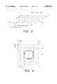
- FIG. 3shows a segment of a perforated stiffener or heat spreader made in accordance with the present invention
- FIG. 4shows a plan view of an upper side of a TBGA package utilizing a perforated stiffener in accordance with the invention
- FIG. 5is a cross-sectional view of an alternative TBGA package made in accordance with the present invention.
- FIG. 6is a perspective view the underneath side of a portion of the alternative TBGA package shown in FIG. 5.
- FIG. 1shows a cross-sectional view of one type of TBGA package 10 which could incorporate the present invention.
- the type of package shown in FIG. 1is sometimes referred to as a "flip chip", and is characterized by not employing any wire bonds.
- the TBGA package 10includes a chip 12 having bumps 14 (e.g. gold bumps) that represent the interconnection points of the chip. These interconnection points may also be pads, and thus may be referred to as first surface pads (the "first surface” referring to a surface of the chip 12).
- the bumps or pads 14connect to selected traces 18 (not visible in FIG. 1) on one side of one or a two-layer thin tape 16, typically made of a polyimide material or other dielectric 20 sandwiched between two layers of copper 18' and 22.
- the copper layer 18'has a pattern of traces 18 formed thereon (not visible in FIG. 1) that electrically connect selected bumps 14 of the chip 12, through vias 24, to solder balls 26.
- the tape 16thus functions as a mini PCB that selectively connects the bumps 14 of the chip 12 to desired solder balls 26 located on the other side of the tape 16.
- the tape 16 shown in FIG. 1is referred to as a double layer tape (because electrical connections are made on both sides of the tape).
- the solder balls 26,are arranged in a ball grid array, as is known in the art, and are adapted for connection to metal traces or pads 30 on the surface of a printed circuit board (PCB) 32.
- PCBprinted circuit board
- a thin layer or film of solder paste 28may be spread over the PCB traces or pads 32 before soldering the solder balls 26 thereto in order to facilitate the solder connection, as is known in the art.
- the soldering of the balls 26 to the traces or pads 30is performed in conventional manner, e.g., through a solder reflow operation.
- a suitable encapsulant 13may be used to hold the chip 12 in its desired position against the tape 16. Further, an adhesive 36 may be used to hold a stiffener 34 against the tape 16, thereby imparting desired rigidity into the IC package.
- the stiffener 34is usually made from metal or other material having a coefficient of thermal expansion matching the coefficient of thermal expansion of the PCB 32.
- a filler material 15, e.g., epoxy or other suitable protective material or encapsulant,may then be placed over the chip 12 in order to fill in voids and cover the chip 12 to help protect it.
- the die or chip 12is encapsulated with encapsulant 13 and/or 15 after attachment is made to the bumps 14.
- the stiffener 34also functions as a heat sink or heat spreader. That is, the stiffener 34 helps keep the surface of the chip cool during operation, which in turn helps maintain the junction temperature of the various devices included on the chip at safe operating levels.
- the main purpose of the stiffener 34is to add rigidity and planarity to the TBGA package 10.
- FIG. 2shows a plan view of the array of solder balls 26 that is formed on the underneath side (the side that attaches to the PCB) of the TBGA package 10.
- the solder balls 26are typically arranged in rows 38 and columns 39.
- An opening 23is generally included in the tape 16, as seen in FIG. 2. The placement of the chip 12 in the center of the opposite side of the tape is thus readily evident through this opening, as shown in FIG. 2. If there is a conductive layer 22 on the underneath side of the tape 16, e.g., when two-layer tape is used, then such layer may be used as a voltage or ground plane.
- suitable open regions 27are made in the layer 22 to prevent the solder balls from shorting to the layer 22, and/or from shorting to each other through the layer 22. (Only a few of the open regions 27 are shown in FIG. 2, but it is to be understood that such open regions would be used whenever the copper layer 22 remains on the underneath side of the tape as a voltage or ground plane.)
- the present inventionadvantageously provides vent holes or openings 40 in a stiffener 34', as illustrated in FIG. 3.
- Such openings 40are typically arranged in an linear array of rows and columns, as shown in FIG. 3, which shows a portion of a stiffener 34' made in accordance with the present invention.
- the vent holes 40need not necessarily be arranged in a linear array as shown in FIG. 3, but may be arranged in any suitable pattern, whether an ordered pattern or a random pattern.
- the vent holes 40have a diameter d3 and are spaced in accordance with any desired grid spacing and/or pattern.
- a linear patternmay be employed, wherein rows of vent holes 40 are separated from each other by a distance d1, and wherein columns of vent holes are similarly separated by a distance d2.
- the values of d1 and d2are on the order of 50 mils (0.050 inches, or 1.27 mm), but may assume values from 20 mils (0.020 inches, or 0.51 mm) to 200 mils (0.200 inches, or 5.08 mm).
- the diameter d3 of the vent holes 40is typically on the order of 20 mils (0.020 inches, or 0.51 mm), but may range from 0.010 inches (0.254 mm) to 0.100 inches (2.54 mm).
- the thickness of the stiffener 34is typically around 10-20 mils (0.254-0.51 mm), but may assume any value as is known in the art. (The thickness of the stiffener is typically an industry specified value). Representative materials from which the stiffener 34 may be made include aluminum, copper, and nickel, or alloys thereof, and sometimes these metals may include a plating of gold or nickel.
- the size and spacing of the vent holes 40is selected so as not to materially alter the thermal, stiffness and planarity properties of the stiffener 34'. It is important that the vent holes 40 not be plugged up with any other material, unless that material is moisture permeable. Otherwise, the vent holes will not be able to perform their intended function of providing an escape vent through which water vapor or other gases may be released.
- FIG. 4a plan view of an upper side of a TBGA package utilizing a perforated stiffener 34' in accordance with the invention is illustrated. Note that an opening 42 is centrally located in the stiffener 34' and the chip 12 is positioned within this opening. Thus, for the configuration shown in FIG. 4, the stiffener 34' surrounds the chip 12.
- vent holes 40 shown in FIG. 4is meant to teach the concept of using vent holes, but is not necessarily meant to show the actual number and arrangement of holes that may be used in an TBGA package.
- a typical TBGA packagemay have outer dimensions of 15 mm by 15 mm, up to 50 mm by 50 mm, with an array of 11 by 11 up to 49 by 49 solder balls on its lower surface for attachment to a PCB.
- the number of vent holes 40 used in the stiffener 34'may range from one vent hole per solder ball (1:1) to one vent hole per four solder balls (1:4), or (in some instances) one vent hole per eight solder balls (1:8) or one vent hole per sixteen solder balls (1:16).
- vent holes 40allow evaporated moisture or other gases to escape from the package during 2nd level packaging, rather than being trapped therein.
- one vent holemay be sufficient in some instances to serve this purpose; but generally, an array or pattern of many vent holes will be used.
- FIG. 5a cross-sectional view of an alternative TBGA package 10' made in accordance with the present invention is illustrated.
- the chip 12is positioned within an opening 46 of a tape 16'.
- the tape 16'may have two conductive layers 18' and 22 separated by a dielectric or insulative layer 20, as does the tape 16 of FIG. 1, the individual traces 18 placed on the conductive layer 18' for the tape 16' shown in FIG. 5 are on the same side as, and thus connect directly to, the solder balls 26 without the use of, or need for, vias 24 to connect from one side of the tape 16 to the other.
- a via 24may be used to connect to such layer.
- other suitable electrical connection meansmay be used to electrically connect to the layer 22, e.g., a conductive strap or wire may be soldered to the layer 22 and pass through the opening 46 to connect to a desired trace 18 or contact point on the opposite side of the tape 16'.
- the chip 12is secured to the stiffener 34' through the use of a suitable die attach material 38.
- the tape 16'is secured to the stiffener 34' through the use of a suitable adhesive 36.
- the adhesive 36may be the same as, or different from, the die attach material 38.
- the bumps 14, or other attachment pads on the surface of the chip 12i.e., the first surface pads
- the trace extensions 44may comprise conductive wires that are bonded at each end to the trace 18 and the pad 14, or they may comprise actual extensions of the trace 18 on the tape 16.
- a suitable encapsulant 39as is known in the art, may also be used to fill in any remaining space or voids within the opening 46, as well as to encapsulate or cover (and thus protect) the chip 12.
- the adhesive 36 used to secure the stiffener 34' to the tape 16is preferably made from a material that is moisture permeable, thereby allowing moisture to readily pass therethrough. In this way, the adhesive 36 does not block or prevent the vent holes 40 from performing their intended function of allowing gases, e.g., water vapor, to escape therethrough.
- Any suitable commercially-available adhesive 36, and/or die attach agent or material 38, and/or encapsulant 39,may be used within the TBGA package in accordance with the present invention.
- stiffener 34'may also serve the function of a heat sink. This is accomplished by extending the spreader 34' over the top surface of the chip 12 (i.e., the surface opposite the chip contact pads 14) and selecting the die attach material 38 so that it exhibits appropriate thermal conducting characteristics.
- FIG. 6shows a partial perspective view of the chip 10' of FIG. 5 viewed from the bottom side of the chip, i.e., viewed from that side of the chip 10' that attaches to the PCB 32.
- no encapsulant or filler 39is shown in FIG. 6, but it is to be understood that such encapsulant is used to fill in the remaining space within the opening 46 of the tape 16'.
- extensions 44 of the individual traces 18 on the bottom surface of the tape 16'are connected to the bumps or other contact points 14 on the bottom surface of the chip 12.
- the other conductive surface 22 of the tape 16'i.e., the top surface of the tape 16' as oriented in FIG. 5, but which appears as the bottom surface as oriented in FIG. 6) typically has one or more conductive planes 22 thereon that may serve as voltage and/or ground planes, as explained previously.
- each of the traces 18spread out across the surface of the tape 16 and interconnect to respective solder balls 26.
- the solder balls 26are arranged in a suitable pattern or array, e.g., as shown in FIG. 2, so that they align with and may be soldered to appropriate pads 30 on the PCB 32, thereby providing both electrical and mechanical attachment of the chip 10' to the PCB 32.
- the present inventionadvantageously provides a TBGA IC package that allows moisture to vent therefrom during 2nd level packaging, thereby preventing moisture or gases (e.g., absorbed within the hygroscopic materials of the package and evaporated therefrom during 2nd level packaging) from being entrapped within the package during a 2nd level packaging operation, which entrapment could otherwise introduce numerous failure modes.
- moisture or gasese.g., absorbed within the hygroscopic materials of the package and evaporated therefrom during 2nd level packaging
- the inventionnot only provides a TBGA IC package wherein water vapor or other gases can readily vent during the 2nd level packaging operation, but also does so without materially altering the heat spreading and/or heat sinking capacity of the stiffener and/or heat spreader used with such package.
- the inventionprovides a TBGA IC package and a method of making a TBGA IC package during 1st level packaging that improves the yield of such TBGA package during 2nd level packaging.
Landscapes
- Engineering & Computer Science (AREA)
- Physics & Mathematics (AREA)
- Condensed Matter Physics & Semiconductors (AREA)
- General Physics & Mathematics (AREA)
- Computer Hardware Design (AREA)
- Microelectronics & Electronic Packaging (AREA)
- Power Engineering (AREA)
- Manufacturing & Machinery (AREA)
- Wire Bonding (AREA)
Abstract
Description
Claims (20)
Priority Applications (1)
| Application Number | Priority Date | Filing Date | Title |
|---|---|---|---|
| US08/934,529US5835355A (en) | 1997-09-22 | 1997-09-22 | Tape ball grid array package with perforated metal stiffener |
Applications Claiming Priority (1)
| Application Number | Priority Date | Filing Date | Title |
|---|---|---|---|
| US08/934,529US5835355A (en) | 1997-09-22 | 1997-09-22 | Tape ball grid array package with perforated metal stiffener |
Publications (1)
| Publication Number | Publication Date |
|---|---|
| US5835355Atrue US5835355A (en) | 1998-11-10 |
Family
ID=25465694
Family Applications (1)
| Application Number | Title | Priority Date | Filing Date |
|---|---|---|---|
| US08/934,529Expired - LifetimeUS5835355A (en) | 1997-09-22 | 1997-09-22 | Tape ball grid array package with perforated metal stiffener |
Country Status (1)
| Country | Link |
|---|---|
| US (1) | US5835355A (en) |
Cited By (162)
| Publication number | Priority date | Publication date | Assignee | Title |
|---|---|---|---|---|
| US5977633A (en)* | 1996-08-15 | 1999-11-02 | Nec Corporation | Semiconductor device with metal base substrate having hollows |
| US6048656A (en)* | 1999-05-11 | 2000-04-11 | Micron Technology, Inc. | Void-free underfill of surface mounted chips |
| US6078506A (en)* | 1997-02-13 | 2000-06-20 | Nec Corporation | Tape-ball grid array type semiconductor device having reinforcement plate with slits |
| US6097085A (en)* | 1997-08-29 | 2000-08-01 | Kabushiki Kaisha Toshiba | Electronic device and semiconductor package |
| US6208022B1 (en)* | 1997-03-27 | 2001-03-27 | Nec Corporation | Electronic-circuit assembly |
| US6259154B1 (en)* | 1998-04-21 | 2001-07-10 | Nec Corporation | Semiconductor device and method of manufacturing the same |
| US6278182B1 (en)* | 1999-01-06 | 2001-08-21 | Walsin Advanced Electronics Ltd. | Lead frame type semiconductor package |
| US6285081B1 (en) | 1999-07-13 | 2001-09-04 | Micron Technology, Inc. | Deflectable interconnect |
| US6291895B1 (en)* | 1998-02-25 | 2001-09-18 | Fujitsu Limited | Method of fabricating semiconductor having through hole |
| US6308938B1 (en)* | 1997-09-26 | 2001-10-30 | Mitsubishi Denki Kabushiki Kaisha | Semiconductor integrated circuit device |
| US6329713B1 (en)* | 1998-10-21 | 2001-12-11 | International Business Machines Corporation | Integrated circuit chip carrier assembly comprising a stiffener attached to a dielectric substrate |
| US6355199B1 (en)* | 1999-02-12 | 2002-03-12 | St. Assembly Test Services Pte Ltd | Method of molding flexible circuit with molded stiffener |
| US6396136B2 (en)* | 1998-12-31 | 2002-05-28 | Texas Instruments Incorporated | Ball grid package with multiple power/ground planes |
| US6395578B1 (en) | 1999-05-20 | 2002-05-28 | Amkor Technology, Inc. | Semiconductor package and method for fabricating the same |
| US6396701B1 (en)* | 1999-11-12 | 2002-05-28 | Fujitsu Limited | Semiconductor unit and cooling device |
| US6414849B1 (en)* | 1999-10-29 | 2002-07-02 | Stmicroelectronics, Inc. | Low stress and low profile cavity down flip chip and wire bond BGA package |
| US6442043B1 (en)* | 1999-08-11 | 2002-08-27 | Fujikura Limited | Chip assembly module of bump connection type using a multi-layer printed circuit substrate |
| US6448506B1 (en) | 2000-12-28 | 2002-09-10 | Amkor Technology, Inc. | Semiconductor package and circuit board for making the package |
| US6452278B1 (en) | 2000-06-30 | 2002-09-17 | Amkor Technology, Inc. | Low profile package for plural semiconductor dies |
| US20020135065A1 (en)* | 2000-12-01 | 2002-09-26 | Zhao Sam Ziqun | Thermally and electrically enhanced ball grid array packaging |
| US20020140085A1 (en)* | 2001-04-02 | 2002-10-03 | Lee Sang Ho | Semiconductor package including passive elements and method of manufacture |
| US6469258B1 (en) | 1999-08-24 | 2002-10-22 | Amkor Technology, Inc. | Circuit board for semiconductor package |
| US6486537B1 (en) | 2001-03-19 | 2002-11-26 | Amkor Technology, Inc. | Semiconductor package with warpage resistant substrate |
| US6501184B1 (en) | 1999-05-20 | 2002-12-31 | Amkor Technology, Inc. | Semiconductor package and method for manufacturing the same |
| US6506626B1 (en)* | 2000-05-12 | 2003-01-14 | Siliconware Precision Industries Co., Ltd. | Semiconductor package structure with heat-dissipation stiffener and method of fabricating the same |
| US20030015785A1 (en)* | 1995-11-29 | 2003-01-23 | Hitachi, Ltd. | BGA type semiconductor device and electronic equipment using the same |
| US6512288B1 (en) | 1999-06-07 | 2003-01-28 | Amkor Technology, Inc. | Circuit board semiconductor package |
| US6515356B1 (en)* | 1999-05-07 | 2003-02-04 | Amkor Technology, Inc. | Semiconductor package and method for fabricating the same |
| US20030047814A1 (en)* | 2001-09-10 | 2003-03-13 | Kwon Heung Kyu | Method for manufacturing flip chip package devices with a heat spreader |
| US20030057550A1 (en)* | 2000-12-22 | 2003-03-27 | Broadcom Corporation | Ball grid array package enhanced with a thermal and electrical connector |
| US6562661B2 (en) | 2000-02-24 | 2003-05-13 | Micron Technology, Inc. | Tape stiffener, semiconductor device component assemblies including same, and stereolithographic methods for fabricating same |
| US6564454B1 (en)* | 2000-12-28 | 2003-05-20 | Amkor Technology, Inc. | Method of making and stacking a semiconductor package |
| US6576998B1 (en) | 2002-02-28 | 2003-06-10 | Amkor Technology, Inc. | Thin semiconductor package with semiconductor chip and electronic discrete device |
| US20030111726A1 (en)* | 2001-12-18 | 2003-06-19 | Khan Reza-Ur Rahman | Ball grid array package substrates and method of making the same |
| US20030146503A1 (en)* | 2002-02-01 | 2003-08-07 | Broadcom Corporation | Ball grid array package with stepped stiffener layer |
| US20030146506A1 (en)* | 2002-02-01 | 2003-08-07 | Broadcom Corporation | Ball grid array package fabrication with IC die support structures |
| US20030146511A1 (en)* | 2002-02-01 | 2003-08-07 | Broadcom Corporation | Ball grid array package with multiple interposers |
| US20030164548A1 (en)* | 2002-03-04 | 2003-09-04 | Lee Teck Kheng | Flip chip packaging using recessed interposer terminals |
| US20030179556A1 (en)* | 2002-03-21 | 2003-09-25 | Broadcom Corporation | Enhanced die-up ball grid array package with two substrates and method for making the same |
| US20030201525A1 (en)* | 2002-04-25 | 2003-10-30 | Micron Technology, Inc. | Standoffs for centralizing internals in packaging process |
| US20040007776A1 (en)* | 2002-07-11 | 2004-01-15 | Tong Chen | Multi-substrate layer semiconductor packages and method for making same |
| US20040007771A1 (en)* | 1999-08-24 | 2004-01-15 | Amkor Technology, Inc. | Semiconductor package and method for fabricating the smae |
| US6683795B1 (en) | 2002-04-10 | 2004-01-27 | Amkor Technology, Inc. | Shield cap and semiconductor package including shield cap |
| US6687133B1 (en)* | 2002-11-15 | 2004-02-03 | Lsi Logic Corporation | Ground plane on 2 layer PBGA |
| US20040046262A1 (en)* | 2002-03-08 | 2004-03-11 | Kabushiki Kaisha Toshiba | Chip mounting substrate, first level assembly, and second level assembly |
| US6720650B2 (en)* | 2000-07-13 | 2004-04-13 | Nec Electronics Corporation | Semiconductor device having heat spreader attached thereto and method of manufacturing the same |
| US6747352B1 (en) | 2002-08-19 | 2004-06-08 | Amkor Technology, Inc. | Integrated circuit having multiple power/ground connections to a single external terminal |
| US6756251B2 (en) | 2001-08-21 | 2004-06-29 | Micron Technology, Inc. | Method of manufacturing microelectronic devices, including methods of underfilling microelectronic components through an underfill aperture |
| US6779783B2 (en)* | 2001-11-27 | 2004-08-24 | Via Technologies, Inc. | Method and structure for tape ball grid array package |
| US6784534B1 (en) | 2002-02-06 | 2004-08-31 | Amkor Technology, Inc. | Thin integrated circuit package having an optically transparent window |
| US20040195701A1 (en)* | 2003-01-07 | 2004-10-07 | Attarwala Abbas Ismail | Electronic package and method |
| US20040212051A1 (en)* | 2000-12-22 | 2004-10-28 | Broadcom Corporation | Ball grid array package with patterned stiffener layer |
| US20040219713A1 (en)* | 2002-01-09 | 2004-11-04 | Micron Technology, Inc. | Elimination of RDL using tape base flip chip on flex for die stacking |
| US6853070B2 (en) | 2001-02-15 | 2005-02-08 | Broadcom Corporation | Die-down ball grid array package with die-attached heat spreader and method for making the same |
| US20050051604A1 (en)* | 2003-09-09 | 2005-03-10 | Texas Instruments Incorporated | Method and system for forming ball grid array ("BGA") packages |
| US20050051893A1 (en)* | 2003-09-05 | 2005-03-10 | Taiwan Semiconductor Manufacturing Co. | SBGA design for low-k integrated circuits (IC) |
| US20050056943A1 (en)* | 2003-09-15 | 2005-03-17 | International Business Machines Corporation | Integrated electronic chip and interconnect device and process for making the same |
| US20050156322A1 (en)* | 2001-08-31 | 2005-07-21 | Smith Lee J. | Thin semiconductor package including stacked dies |
| US20050224956A1 (en)* | 2004-04-02 | 2005-10-13 | Chin-Li Kao | Chip package structure and chip packaging process |
| US6967124B1 (en) | 2001-06-19 | 2005-11-22 | Amkor Technology, Inc. | Imprinted integrated circuit substrate and method for imprinting an integrated circuit substrate |
| US6975035B2 (en) | 2002-03-04 | 2005-12-13 | Micron Technology, Inc. | Method and apparatus for dielectric filling of flip chip on interposer assembly |
| US6982485B1 (en) | 2002-02-13 | 2006-01-03 | Amkor Technology, Inc. | Stacking structure for semiconductor chips and a semiconductor package using it |
| US6989593B2 (en) | 2000-12-22 | 2006-01-24 | Broadcom Corporation | Die-up ball grid array package with patterned stiffener opening |
| US20060017155A1 (en)* | 2004-07-21 | 2006-01-26 | Advanced Semiconductor Engineering, Inc. | Flip chip package capable of measuring bond line thickness of thermal interface material |
| US20060084254A1 (en)* | 2004-01-06 | 2006-04-20 | Attarwala Abbas I | Method for making electronic packages |
| US7042072B1 (en) | 2002-08-02 | 2006-05-09 | Amkor Technology, Inc. | Semiconductor package and method of manufacturing the same which reduces warpage |
| US20060102998A1 (en)* | 2004-10-14 | 2006-05-18 | Harry Hedler | Flip-chip component |
| US20060125088A1 (en)* | 2004-12-14 | 2006-06-15 | Siliconware Precision Industries Co., Ltd. | Heat dissipating semiconductor package and fabrication method thereof |
| US7087460B2 (en) | 2002-03-04 | 2006-08-08 | Micron Technology, Inc. | Methods for assembly and packaging of flip chip configured dice with interposer |
| US7112520B2 (en) | 2002-03-04 | 2006-09-26 | Micron Technology, Inc. | Semiconductor die packages with recessed interconnecting structures and methods for assembling the same |
| US7115986B2 (en) | 2001-05-02 | 2006-10-03 | Micron Technology, Inc. | Flexible ball grid array chip scale packages |
| US7132744B2 (en) | 2000-12-22 | 2006-11-07 | Broadcom Corporation | Enhanced die-up ball grid array packages and method for making the same |
| US20060250139A1 (en)* | 2001-08-10 | 2006-11-09 | Micron Technology, Inc. | Bond pad structure comprising multiple bond pads with metal overlap |
| US7145225B2 (en) | 2002-03-04 | 2006-12-05 | Micron Technology, Inc. | Interposer configured to reduce the profiles of semiconductor device assemblies and packages including the same and methods |
| US7145238B1 (en) | 2004-05-05 | 2006-12-05 | Amkor Technology, Inc. | Semiconductor package and substrate having multi-level vias |
| US20060273458A1 (en)* | 2005-06-07 | 2006-12-07 | Wen-Shien Huang | Substrate structure of semiconductor package |
| US7185426B1 (en) | 2002-05-01 | 2007-03-06 | Amkor Technology, Inc. | Method of manufacturing a semiconductor package |
| US7196415B2 (en) | 2002-03-22 | 2007-03-27 | Broadcom Corporation | Low voltage drop and high thermal performance ball grid array package |
| US20070120240A1 (en)* | 2005-11-29 | 2007-05-31 | 3M Innovative Properties Company | Circuit substrate and method of manufacture |
| US20070134860A1 (en)* | 2004-01-30 | 2007-06-14 | Fu-Liang Yang | Methods and Structures for Planar and Multiple-Gate Transistors Formed on SOI |
| US20070145548A1 (en)* | 2003-12-22 | 2007-06-28 | Amkor Technology, Inc. | Stack-type semiconductor package and manufacturing method thereof |
| US7259448B2 (en)* | 2001-05-07 | 2007-08-21 | Broadcom Corporation | Die-up ball grid array package with a heat spreader and method for making the same |
| US7320933B2 (en) | 2002-08-20 | 2008-01-22 | Micron Technology, Inc. | Double bumping of flexible substrate for first and second level interconnects |
| USRE40112E1 (en) | 1999-05-20 | 2008-02-26 | Amkor Technology, Inc. | Semiconductor package and method for fabricating the same |
| US7334326B1 (en) | 2001-06-19 | 2008-02-26 | Amkor Technology, Inc. | Method for making an integrated circuit substrate having embedded passive components |
| US20080093733A1 (en)* | 2006-10-23 | 2008-04-24 | Via Technologies, Inc. | Chip package and manufacturing method thereof |
| US20080142960A1 (en)* | 2003-04-18 | 2008-06-19 | Freescale Semiconductor, Inc. | Circuit device with at least partial packaging and method for forming |
| US7399661B2 (en) | 2002-05-01 | 2008-07-15 | Amkor Technology, Inc. | Method for making an integrated circuit substrate having embedded back-side access conductors and vias |
| US7411281B2 (en) | 2004-06-21 | 2008-08-12 | Broadcom Corporation | Integrated circuit device package having both wire bond and flip-chip interconnections and method of making the same |
| US7432586B2 (en) | 2004-06-21 | 2008-10-07 | Broadcom Corporation | Apparatus and method for thermal and electromagnetic interference (EMI) shielding enhancement in die-up array packages |
| US20080246139A1 (en)* | 2007-04-03 | 2008-10-09 | Don Craven | Polar hybrid grid array package |
| US20080297489A1 (en)* | 2007-05-28 | 2008-12-04 | Fuji Xerox Co., Ltd. | Data input system |
| US7482686B2 (en) | 2004-06-21 | 2009-01-27 | Braodcom Corporation | Multipiece apparatus for thermal and electromagnetic interference (EMI) shielding enhancement in die-up array packages and method of making the same |
| US7501338B1 (en) | 2001-06-19 | 2009-03-10 | Amkor Technology, Inc. | Semiconductor package substrate fabrication method |
| US20090091031A1 (en)* | 2003-08-28 | 2009-04-09 | Noriyuki Takahashi | Semiconductor device |
| US20090095524A1 (en)* | 2007-10-12 | 2009-04-16 | Fujitsu Limited | Core substrate and method of producing the same |
| US7548430B1 (en) | 2002-05-01 | 2009-06-16 | Amkor Technology, Inc. | Buildup dielectric and metallization process and semiconductor package |
| US7550845B2 (en) | 2002-02-01 | 2009-06-23 | Broadcom Corporation | Ball grid array package with separated stiffener layer |
| US7550857B1 (en) | 2006-11-16 | 2009-06-23 | Amkor Technology, Inc. | Stacked redistribution layer (RDL) die assembly package |
| US7589398B1 (en) | 2006-10-04 | 2009-09-15 | Amkor Technology, Inc. | Embedded metal features structure |
| US7633765B1 (en) | 2004-03-23 | 2009-12-15 | Amkor Technology, Inc. | Semiconductor package including a top-surface metal layer for implementing circuit features |
| US7656236B2 (en) | 2007-05-15 | 2010-02-02 | Teledyne Wireless, Llc | Noise canceling technique for frequency synthesizer |
| US7670962B2 (en) | 2002-05-01 | 2010-03-02 | Amkor Technology, Inc. | Substrate having stiffener fabrication method |
| US7750250B1 (en) | 2006-12-22 | 2010-07-06 | Amkor Technology, Inc. | Blind via capture pad structure |
| US7752752B1 (en) | 2007-01-09 | 2010-07-13 | Amkor Technology, Inc. | Method of fabricating an embedded circuit pattern |
| US7786591B2 (en) | 2004-09-29 | 2010-08-31 | Broadcom Corporation | Die down ball grid array package |
| US20100289134A1 (en)* | 2009-05-15 | 2010-11-18 | Seng Guan Chow | Integrated circuit packaging system with reinforced encapsulant having embedded interconnect and method of manufacture thereof |
| US7915718B2 (en) | 2002-03-04 | 2011-03-29 | Micron Technology, Inc. | Apparatus for flip-chip packaging providing testing capability |
| CN102082102A (en)* | 2009-11-25 | 2011-06-01 | 新科金朋有限公司 | Semiconductor device and method of forming compliant stress relief buffer |
| US7960827B1 (en) | 2009-04-09 | 2011-06-14 | Amkor Technology, Inc. | Thermal via heat spreader package and method |
| US20110182042A1 (en)* | 2007-07-05 | 2011-07-28 | Occam Portfolio Llc | Electronic Assemblies without Solder and Methods for their Manufacture |
| US20110278714A1 (en)* | 2010-05-14 | 2011-11-17 | Chipmos Technologies Inc. | Chip package device and manufacturing method thereof |
| US20110316144A1 (en)* | 2010-06-25 | 2011-12-29 | Samsung Electronics Co., Ltd. | Flexible heat sink having ventilation ports and semiconductor package including the same |
| US8179045B2 (en) | 2008-04-22 | 2012-05-15 | Teledyne Wireless, Llc | Slow wave structure having offset projections comprised of a metal-dielectric composite stack |
| US20120120609A1 (en)* | 2010-11-12 | 2012-05-17 | Unimicron Technology Corporation | Package structure having a semiconductor component embedded therein and method of fabricating the same |
| US8183680B2 (en) | 2006-05-16 | 2012-05-22 | Broadcom Corporation | No-lead IC packages having integrated heat spreader for electromagnetic interference (EMI) shielding and thermal enhancement |
| US8222538B1 (en) | 2009-06-12 | 2012-07-17 | Amkor Technology, Inc. | Stackable via package and method |
| US8294276B1 (en) | 2010-05-27 | 2012-10-23 | Amkor Technology, Inc. | Semiconductor device and fabricating method thereof |
| US8300423B1 (en) | 2010-05-25 | 2012-10-30 | Amkor Technology, Inc. | Stackable treated via package and method |
| US8323771B1 (en) | 2007-08-15 | 2012-12-04 | Amkor Technology, Inc. | Straight conductor blind via capture pad structure and fabrication method |
| US8338229B1 (en) | 2010-07-30 | 2012-12-25 | Amkor Technology, Inc. | Stackable plasma cleaned via package and method |
| US8337657B1 (en) | 2010-10-27 | 2012-12-25 | Amkor Technology, Inc. | Mechanical tape separation package and method |
| US8471154B1 (en) | 2009-08-06 | 2013-06-25 | Amkor Technology, Inc. | Stackable variable height via package and method |
| US8482134B1 (en) | 2010-11-01 | 2013-07-09 | Amkor Technology, Inc. | Stackable package and method |
| US8525318B1 (en) | 2010-11-10 | 2013-09-03 | Amkor Technology, Inc. | Semiconductor device and fabricating method thereof |
| US8536462B1 (en) | 2010-01-22 | 2013-09-17 | Amkor Technology, Inc. | Flex circuit package and method |
| US8535961B1 (en) | 2010-12-09 | 2013-09-17 | Amkor Technology, Inc. | Light emitting diode (LED) package and method |
| US8557629B1 (en) | 2010-12-03 | 2013-10-15 | Amkor Technology, Inc. | Semiconductor device having overlapped via apertures |
| US8623753B1 (en) | 2009-05-28 | 2014-01-07 | Amkor Technology, Inc. | Stackable protruding via package and method |
| US8633598B1 (en) | 2011-09-20 | 2014-01-21 | Amkor Technology, Inc. | Underfill contacting stacking balls package fabrication method and structure |
| US8653674B1 (en) | 2011-09-15 | 2014-02-18 | Amkor Technology, Inc. | Electronic component package fabrication method and structure |
| US8717775B1 (en) | 2010-08-02 | 2014-05-06 | Amkor Technology, Inc. | Fingerprint sensor package and method |
| US8796561B1 (en) | 2009-10-05 | 2014-08-05 | Amkor Technology, Inc. | Fan out build up substrate stackable package and method |
| US8826531B1 (en) | 2005-04-05 | 2014-09-09 | Amkor Technology, Inc. | Method for making an integrated circuit substrate having laminated laser-embedded circuit layers |
| US8872329B1 (en) | 2009-01-09 | 2014-10-28 | Amkor Technology, Inc. | Extended landing pad substrate package structure and method |
| US8890329B2 (en) | 2011-04-26 | 2014-11-18 | Amkor Technology, Inc. | Semiconductor device |
| US20150014031A1 (en)* | 2013-07-10 | 2015-01-15 | Kinsus Interconnect Technology Corp. | Compound carrier board structure of flip-chip chip-scale package and manufacturing method thereof |
| US8937381B1 (en) | 2009-12-03 | 2015-01-20 | Amkor Technology, Inc. | Thin stackable package and method |
| US20150084168A1 (en)* | 2013-09-25 | 2015-03-26 | Min Ding | Package encapsulant relief feature |
| US9013011B1 (en) | 2011-03-11 | 2015-04-21 | Amkor Technology, Inc. | Stacked and staggered die MEMS package and method |
| US9029962B1 (en) | 2011-10-12 | 2015-05-12 | Amkor Technology, Inc. | Molded cavity substrate MEMS package fabrication method and structure |
| US20150270190A1 (en)* | 2014-03-18 | 2015-09-24 | Jin-Gyu Kim | Semiconductor package |
| US9202660B2 (en) | 2013-03-13 | 2015-12-01 | Teledyne Wireless, Llc | Asymmetrical slow wave structures to eliminate backward wave oscillations in wideband traveling wave tubes |
| US9202769B2 (en) | 2009-11-25 | 2015-12-01 | Stats Chippac, Ltd. | Semiconductor device and method of forming thermal lid for balancing warpage and thermal management |
| US20160049316A1 (en)* | 2013-01-07 | 2016-02-18 | Intel Corporation | Embedded package in pcb build up |
| US20160172323A1 (en)* | 2014-12-16 | 2016-06-16 | Intel Corporation | Picture frame stiffeners for microelectronic packages |
| US20160197033A1 (en)* | 2013-07-10 | 2016-07-07 | Kinsus Interconnect Technology Corp. | Compound carrier board structure of flip-chip chip-scale package and manufacturing method thereof |
| US9391043B2 (en) | 2012-11-20 | 2016-07-12 | Amkor Technology, Inc. | Semiconductor device and manufacturing method thereof |
| US9466545B1 (en) | 2007-02-21 | 2016-10-11 | Amkor Technology, Inc. | Semiconductor package in package |
| US9508626B2 (en) | 2010-04-23 | 2016-11-29 | STATS ChipPAC Pte. Ltd. | Semiconductor device and method of forming openings in thermally-conductive frame of FO-WLCSP to dissipate heat and reduce package height |
| US9543242B1 (en) | 2013-01-29 | 2017-01-10 | Amkor Technology, Inc. | Semiconductor package and fabricating method thereof |
| US9691635B1 (en) | 2002-05-01 | 2017-06-27 | Amkor Technology, Inc. | Buildup dielectric layer having metallization pattern semiconductor package fabrication method |
| US9691734B1 (en) | 2009-12-07 | 2017-06-27 | Amkor Technology, Inc. | Method of forming a plurality of electronic component packages |
| US9704842B2 (en) | 2013-11-04 | 2017-07-11 | Amkor Technology, Inc. | Interposer, manufacturing method thereof, semiconductor package using the same, and method for fabricating the semiconductor package |
| US9704747B2 (en) | 2013-03-29 | 2017-07-11 | Amkor Technology, Inc. | Semiconductor device and manufacturing method thereof |
| US9721872B1 (en) | 2011-02-18 | 2017-08-01 | Amkor Technology, Inc. | Methods and structures for increasing the allowable die size in TMV packages |
| US9748154B1 (en) | 2010-11-04 | 2017-08-29 | Amkor Technology, Inc. | Wafer level fan out semiconductor device and manufacturing method thereof |
| US9960328B2 (en) | 2016-09-06 | 2018-05-01 | Amkor Technology, Inc. | Semiconductor device and manufacturing method thereof |
| US20190190354A1 (en)* | 2017-12-18 | 2019-06-20 | Melexis Bulgaria Ltd. | Reinforced electronic device for an electrical motor |
| US20190341353A1 (en)* | 2018-05-04 | 2019-11-07 | Samsung Electronics Co., Ltd. | Fan-out semiconductor package |
| US10811277B2 (en) | 2004-03-23 | 2020-10-20 | Amkor Technology, Inc. | Encapsulated semiconductor package |
| US11081370B2 (en) | 2004-03-23 | 2021-08-03 | Amkor Technology Singapore Holding Pte. Ltd. | Methods of manufacturing an encapsulated semiconductor device |
Citations (20)
| Publication number | Priority date | Publication date | Assignee | Title |
|---|---|---|---|---|
| US4953060A (en)* | 1989-05-05 | 1990-08-28 | Ncr Corporation | Stackable integrated circuit chip package with improved heat removal |
| US5045921A (en)* | 1989-12-26 | 1991-09-03 | Motorola, Inc. | Pad array carrier IC device using flexible tape |
| US5105259A (en)* | 1990-09-28 | 1992-04-14 | Motorola, Inc. | Thermally enhanced semiconductor device utilizing a vacuum to ultimately enhance thermal dissipation |
| JPH04245668A (en)* | 1991-01-31 | 1992-09-02 | Ibiden Co Ltd | Board for placing electronic component using heat sink slag |
| US5216278A (en)* | 1990-12-04 | 1993-06-01 | Motorola, Inc. | Semiconductor device having a pad array carrier package |
| US5285350A (en)* | 1992-08-28 | 1994-02-08 | Aavid Engineering, Inc. | Heat sink plate for multiple semi-conductors |
| US5369550A (en)* | 1992-09-02 | 1994-11-29 | Vlsi Technology, Inc. | Method and apparatus for cooling a molded-plastic integrated-circuit package |
| US5397917A (en)* | 1993-04-26 | 1995-03-14 | Motorola, Inc. | Semiconductor package capable of spreading heat |
| US5410451A (en)* | 1993-12-20 | 1995-04-25 | Lsi Logic Corporation | Location and standoff pins for chip on tape |
| US5485037A (en)* | 1993-04-12 | 1996-01-16 | Amkor Electronics, Inc. | Semiconductor device having a thermal dissipator and electromagnetic shielding |
| US5490324A (en)* | 1993-09-15 | 1996-02-13 | Lsi Logic Corporation | Method of making integrated circuit package having multiple bonding tiers |
| US5506756A (en)* | 1994-01-25 | 1996-04-09 | Intel Corporation | Tape BGA package die-up/die down |
| US5511306A (en)* | 1994-04-05 | 1996-04-30 | Compaq Computer Corporation | Masking of circuit board vias to reduce heat-induced board and chip carrier package warp during wavesolder process |
| US5550406A (en)* | 1992-06-04 | 1996-08-27 | Lsi Logic Corporation | Multi-layer tab tape having distinct signal, power and ground planes and wafer probe card with multi-layer substrate |
| US5598321A (en)* | 1995-09-11 | 1997-01-28 | National Semiconductor Corporation | Ball grid array with heat sink |
| US5602422A (en)* | 1995-06-16 | 1997-02-11 | Minnesota Mining And Manufacturing Company | Flexible leads for tape ball grid array circuit |
| US5620928A (en)* | 1995-05-11 | 1997-04-15 | National Semiconductor Corporation | Ultra thin ball grid array using a flex tape or printed wiring board substrate and method |
| US5640048A (en)* | 1994-07-11 | 1997-06-17 | Sun Microsystems, Inc. | Ball grid array package for a integrated circuit |
| US5652185A (en)* | 1995-04-07 | 1997-07-29 | National Semiconductor Corporation | Maximized substrate design for grid array based assemblies |
| US5673479A (en)* | 1993-12-20 | 1997-10-07 | Lsi Logic Corporation | Method for mounting a microelectronic circuit peripherally-leaded package including integral support member with spacer |
- 1997
- 1997-09-22USUS08/934,529patent/US5835355A/ennot_activeExpired - Lifetime
Patent Citations (20)
| Publication number | Priority date | Publication date | Assignee | Title |
|---|---|---|---|---|
| US4953060A (en)* | 1989-05-05 | 1990-08-28 | Ncr Corporation | Stackable integrated circuit chip package with improved heat removal |
| US5045921A (en)* | 1989-12-26 | 1991-09-03 | Motorola, Inc. | Pad array carrier IC device using flexible tape |
| US5105259A (en)* | 1990-09-28 | 1992-04-14 | Motorola, Inc. | Thermally enhanced semiconductor device utilizing a vacuum to ultimately enhance thermal dissipation |
| US5216278A (en)* | 1990-12-04 | 1993-06-01 | Motorola, Inc. | Semiconductor device having a pad array carrier package |
| JPH04245668A (en)* | 1991-01-31 | 1992-09-02 | Ibiden Co Ltd | Board for placing electronic component using heat sink slag |
| US5550406A (en)* | 1992-06-04 | 1996-08-27 | Lsi Logic Corporation | Multi-layer tab tape having distinct signal, power and ground planes and wafer probe card with multi-layer substrate |
| US5285350A (en)* | 1992-08-28 | 1994-02-08 | Aavid Engineering, Inc. | Heat sink plate for multiple semi-conductors |
| US5369550A (en)* | 1992-09-02 | 1994-11-29 | Vlsi Technology, Inc. | Method and apparatus for cooling a molded-plastic integrated-circuit package |
| US5485037A (en)* | 1993-04-12 | 1996-01-16 | Amkor Electronics, Inc. | Semiconductor device having a thermal dissipator and electromagnetic shielding |
| US5397917A (en)* | 1993-04-26 | 1995-03-14 | Motorola, Inc. | Semiconductor package capable of spreading heat |
| US5490324A (en)* | 1993-09-15 | 1996-02-13 | Lsi Logic Corporation | Method of making integrated circuit package having multiple bonding tiers |
| US5410451A (en)* | 1993-12-20 | 1995-04-25 | Lsi Logic Corporation | Location and standoff pins for chip on tape |
| US5673479A (en)* | 1993-12-20 | 1997-10-07 | Lsi Logic Corporation | Method for mounting a microelectronic circuit peripherally-leaded package including integral support member with spacer |
| US5506756A (en)* | 1994-01-25 | 1996-04-09 | Intel Corporation | Tape BGA package die-up/die down |
| US5511306A (en)* | 1994-04-05 | 1996-04-30 | Compaq Computer Corporation | Masking of circuit board vias to reduce heat-induced board and chip carrier package warp during wavesolder process |
| US5640048A (en)* | 1994-07-11 | 1997-06-17 | Sun Microsystems, Inc. | Ball grid array package for a integrated circuit |
| US5652185A (en)* | 1995-04-07 | 1997-07-29 | National Semiconductor Corporation | Maximized substrate design for grid array based assemblies |
| US5620928A (en)* | 1995-05-11 | 1997-04-15 | National Semiconductor Corporation | Ultra thin ball grid array using a flex tape or printed wiring board substrate and method |
| US5602422A (en)* | 1995-06-16 | 1997-02-11 | Minnesota Mining And Manufacturing Company | Flexible leads for tape ball grid array circuit |
| US5598321A (en)* | 1995-09-11 | 1997-01-28 | National Semiconductor Corporation | Ball grid array with heat sink |
Non-Patent Citations (2)
| Title |
|---|
| Huang, et al., "Area Tape Automated Bonding Ball Grid Aray Technology", McGraw-Hill. Inc., pp. 433-464 (1995). |
| Huang, et al., Area Tape Automated Bonding Ball Grid Aray Technology , McGraw Hill. Inc., pp. 433 464 (1995).* |
Cited By (344)
| Publication number | Priority date | Publication date | Assignee | Title |
|---|---|---|---|---|
| US20030015785A1 (en)* | 1995-11-29 | 2003-01-23 | Hitachi, Ltd. | BGA type semiconductor device and electronic equipment using the same |
| US7164194B2 (en)* | 1995-11-29 | 2007-01-16 | Renesas Technology Corp. | BGA type semiconductor device and electronic equipment using the same |
| US5977633A (en)* | 1996-08-15 | 1999-11-02 | Nec Corporation | Semiconductor device with metal base substrate having hollows |
| US6078506A (en)* | 1997-02-13 | 2000-06-20 | Nec Corporation | Tape-ball grid array type semiconductor device having reinforcement plate with slits |
| US6208022B1 (en)* | 1997-03-27 | 2001-03-27 | Nec Corporation | Electronic-circuit assembly |
| US6097085A (en)* | 1997-08-29 | 2000-08-01 | Kabushiki Kaisha Toshiba | Electronic device and semiconductor package |
| US6308938B1 (en)* | 1997-09-26 | 2001-10-30 | Mitsubishi Denki Kabushiki Kaisha | Semiconductor integrated circuit device |
| US6291895B1 (en)* | 1998-02-25 | 2001-09-18 | Fujitsu Limited | Method of fabricating semiconductor having through hole |
| US6259154B1 (en)* | 1998-04-21 | 2001-07-10 | Nec Corporation | Semiconductor device and method of manufacturing the same |
| US6329713B1 (en)* | 1998-10-21 | 2001-12-11 | International Business Machines Corporation | Integrated circuit chip carrier assembly comprising a stiffener attached to a dielectric substrate |
| US6396136B2 (en)* | 1998-12-31 | 2002-05-28 | Texas Instruments Incorporated | Ball grid package with multiple power/ground planes |
| US6278182B1 (en)* | 1999-01-06 | 2001-08-21 | Walsin Advanced Electronics Ltd. | Lead frame type semiconductor package |
| SG108836A1 (en)* | 1999-02-12 | 2005-02-28 | Stats Chippac Ltd | Molded stiffener for flexible circuit molding |
| US6617525B2 (en)* | 1999-02-12 | 2003-09-09 | St. Assembly Test Services Ltd. | Molded stiffener for flexible circuit molding |
| US6355199B1 (en)* | 1999-02-12 | 2002-03-12 | St. Assembly Test Services Pte Ltd | Method of molding flexible circuit with molded stiffener |
| SG89285A1 (en)* | 1999-02-12 | 2002-06-18 | St Assembly Test Services Ltd | Molded stiffener for flexible circuit molding |
| US20040164411A1 (en)* | 1999-05-07 | 2004-08-26 | Amkor Technology, Inc. | Semiconductor package and method for fabricating the same |
| US6717248B2 (en) | 1999-05-07 | 2004-04-06 | Amkor Technology, Inc. | Semiconductor package and method for fabricating the same |
| US7190071B2 (en) | 1999-05-07 | 2007-03-13 | Amkor Technology, Inc. | Semiconductor package and method for fabricating the same |
| US6515356B1 (en)* | 1999-05-07 | 2003-02-04 | Amkor Technology, Inc. | Semiconductor package and method for fabricating the same |
| US6048656A (en)* | 1999-05-11 | 2000-04-11 | Micron Technology, Inc. | Void-free underfill of surface mounted chips |
| US6830955B2 (en) | 1999-05-20 | 2004-12-14 | Amkor Technology, Inc. | Semiconductor package and method for manufacturing the same |
| USRE40112E1 (en) | 1999-05-20 | 2008-02-26 | Amkor Technology, Inc. | Semiconductor package and method for fabricating the same |
| US6762078B2 (en) | 1999-05-20 | 2004-07-13 | Amkor Technology, Inc. | Semiconductor package having semiconductor chip within central aperture of substrate |
| US6501184B1 (en) | 1999-05-20 | 2002-12-31 | Amkor Technology, Inc. | Semiconductor package and method for manufacturing the same |
| US20030001285A1 (en)* | 1999-05-20 | 2003-01-02 | Amkor Technology, Inc. | Semiconductor package and method for manufacturing the same |
| US7061120B2 (en) | 1999-05-20 | 2006-06-13 | Amkor Technology, Inc. | Stackable semiconductor package having semiconductor chip within central through hole of substrate |
| US6395578B1 (en) | 1999-05-20 | 2002-05-28 | Amkor Technology, Inc. | Semiconductor package and method for fabricating the same |
| US6512288B1 (en) | 1999-06-07 | 2003-01-28 | Amkor Technology, Inc. | Circuit board semiconductor package |
| US6501176B2 (en) | 1999-07-13 | 2002-12-31 | Micron Technology, Inc. | Deflectable interconnect |
| US6664131B2 (en) | 1999-07-13 | 2003-12-16 | Micron Technology, Inc. | Method of making ball grid array package with deflectable interconnect |
| US6285081B1 (en) | 1999-07-13 | 2001-09-04 | Micron Technology, Inc. | Deflectable interconnect |
| US6503777B2 (en) | 1999-07-13 | 2003-01-07 | Micron Technology, Inc. | Deflectable interconnect |
| US6630738B2 (en)* | 1999-07-13 | 2003-10-07 | Micron Technology, Inc | Deflectable interconnect |
| US20030092218A1 (en)* | 1999-07-13 | 2003-05-15 | Jackson Timothy L. | Deflectable interconnect |
| US20030089985A1 (en)* | 1999-07-13 | 2003-05-15 | Jackson Timothy L. | Deflectable interconnect |
| US6442043B1 (en)* | 1999-08-11 | 2002-08-27 | Fujikura Limited | Chip assembly module of bump connection type using a multi-layer printed circuit substrate |
| KR100768998B1 (en)* | 1999-08-11 | 2007-10-22 | 가부시키가이샤후지쿠라 | Chip Assembly Module of Bump Connection Type Using a Multi-layer Printed Circuit Substrate |
| EP1076361A3 (en)* | 1999-08-11 | 2003-10-22 | Fujikura Ltd. | Chip assembly module of bump connection type using a multi-layer printed circuit substrate |
| US7211900B2 (en) | 1999-08-24 | 2007-05-01 | Amkor Technology, Inc. | Thin semiconductor package including stacked dies |
| US20050205979A1 (en)* | 1999-08-24 | 2005-09-22 | Shin Won S | Semiconductor package and method for fabricating the same |
| US6798049B1 (en) | 1999-08-24 | 2004-09-28 | Amkor Technology Inc. | Semiconductor package and method for fabricating the same |
| US20040007771A1 (en)* | 1999-08-24 | 2004-01-15 | Amkor Technology, Inc. | Semiconductor package and method for fabricating the smae |
| US6982488B2 (en) | 1999-08-24 | 2006-01-03 | Amkor Technology, Inc. | Semiconductor package and method for fabricating the same |
| US6469258B1 (en) | 1999-08-24 | 2002-10-22 | Amkor Technology, Inc. | Circuit board for semiconductor package |
| US6414849B1 (en)* | 1999-10-29 | 2002-07-02 | Stmicroelectronics, Inc. | Low stress and low profile cavity down flip chip and wire bond BGA package |
| US6396701B1 (en)* | 1999-11-12 | 2002-05-28 | Fujitsu Limited | Semiconductor unit and cooling device |
| US20060121649A1 (en)* | 2000-02-24 | 2006-06-08 | Grigg Ford B | Methods for fabricating stiffeners for flexible substrates |
| US20040142507A1 (en)* | 2000-02-24 | 2004-07-22 | Grigg Ford B. | Tape stiffener, semiconductor device component assemblies including same, and stereolithographic methods for fabricating same |
| US7029954B2 (en) | 2000-02-24 | 2006-04-18 | Micron Technology, Inc. | Tape stiffener, semiconductor device component assemblies including same, and stereolithographic methods for fabricating same |
| US6900078B2 (en) | 2000-02-24 | 2005-05-31 | Micron Technology, Inc. | Tape stiffener, semiconductor device component assemblies including same, and stereolithographic methods for fabricating same |
| US6562661B2 (en) | 2000-02-24 | 2003-05-13 | Micron Technology, Inc. | Tape stiffener, semiconductor device component assemblies including same, and stereolithographic methods for fabricating same |
| US20040212062A1 (en)* | 2000-02-24 | 2004-10-28 | Grigg Ford B. | Tape stiffener and semiconductor device component assemblies including same |
| US20030176021A1 (en)* | 2000-02-24 | 2003-09-18 | Grigg Ford B. | Tape stiffener, semiconductor device component assemblies including same, and stereolithographic methods for fabricating same |
| US20070172992A1 (en)* | 2000-02-24 | 2007-07-26 | Grigg Ford B | Methods for fabricating stiffeners for flexible substrates |
| US7189600B2 (en) | 2000-02-24 | 2007-03-13 | Micron Technology, Inc. | Methods for fabricating stiffeners for flexible substrates |
| US20040224442A1 (en)* | 2000-02-24 | 2004-11-11 | Grigg Ford B. | Tape stiffener, semiconductor device component assemblies including same, and stereolithographic methods for fabricating same |
| US6740962B1 (en) | 2000-02-24 | 2004-05-25 | Micron Technology, Inc. | Tape stiffener, semiconductor device component assemblies including same, and stereolithographic methods for fabricating same |
| US6746899B2 (en) | 2000-02-24 | 2004-06-08 | Micron Technology, Inc. | Tape stiffener, semiconductor device component assemblies including same, and stereolithographic methods for fabricating same |
| US6506626B1 (en)* | 2000-05-12 | 2003-01-14 | Siliconware Precision Industries Co., Ltd. | Semiconductor package structure with heat-dissipation stiffener and method of fabricating the same |
| US6452278B1 (en) | 2000-06-30 | 2002-09-17 | Amkor Technology, Inc. | Low profile package for plural semiconductor dies |
| US6720650B2 (en)* | 2000-07-13 | 2004-04-13 | Nec Electronics Corporation | Semiconductor device having heat spreader attached thereto and method of manufacturing the same |
| US20020135065A1 (en)* | 2000-12-01 | 2002-09-26 | Zhao Sam Ziqun | Thermally and electrically enhanced ball grid array packaging |
| US6882042B2 (en) | 2000-12-01 | 2005-04-19 | Broadcom Corporation | Thermally and electrically enhanced ball grid array packaging |
| US8039949B2 (en) | 2000-12-01 | 2011-10-18 | Broadcom Corporation | Ball grid array package having one or more stiffeners |
| US7629681B2 (en) | 2000-12-01 | 2009-12-08 | Broadcom Corporation | Ball grid array package with patterned stiffener surface and method of assembling the same |
| US8686558B2 (en) | 2000-12-01 | 2014-04-01 | Broadcom Corporation | Thermally and electrically enhanced ball grid array package |
| US7579217B2 (en) | 2000-12-22 | 2009-08-25 | Broadcom Corporation | Methods of making a die-up ball grid array package with printed circuit board attachable heat spreader |
| US7227256B2 (en) | 2000-12-22 | 2007-06-05 | Broadcom Corporation | Die-up ball grid array package with printed circuit board attachable heat spreader |
| US7005737B2 (en) | 2000-12-22 | 2006-02-28 | Broadcom Corporation | Die-up ball grid array package with enhanced stiffener |
| US20030057550A1 (en)* | 2000-12-22 | 2003-03-27 | Broadcom Corporation | Ball grid array package enhanced with a thermal and electrical connector |
| US20040212051A1 (en)* | 2000-12-22 | 2004-10-28 | Broadcom Corporation | Ball grid array package with patterned stiffener layer |
| US6989593B2 (en) | 2000-12-22 | 2006-01-24 | Broadcom Corporation | Die-up ball grid array package with patterned stiffener opening |
| US7038312B2 (en) | 2000-12-22 | 2006-05-02 | Broadcom Corporation | Die-up ball grid array package with attached stiffener ring |
| US7202559B2 (en) | 2000-12-22 | 2007-04-10 | Broadcom Corporation | Method of assembling a ball grid array package with patterned stiffener layer |
| US8310067B2 (en) | 2000-12-22 | 2012-11-13 | Broadcom Corporation | Ball grid array package enhanced with a thermal and electrical connector |
| US7859101B2 (en) | 2000-12-22 | 2010-12-28 | Broadcom Corporation | Die-up ball grid array package with die-attached heat spreader |
| US7102225B2 (en) | 2000-12-22 | 2006-09-05 | Broadcom Corporation | Die-up ball grid array package with printed circuit board attachable heat spreader |
| US7161239B2 (en) | 2000-12-22 | 2007-01-09 | Broadcom Corporation | Ball grid array package enhanced with a thermal and electrical connector |
| US7132744B2 (en) | 2000-12-22 | 2006-11-07 | Broadcom Corporation | Enhanced die-up ball grid array packages and method for making the same |
| US7893546B2 (en) | 2000-12-22 | 2011-02-22 | Broadcom Corporation | Ball grid array package enhanced with a thermal and electrical connector |
| US6906414B2 (en) | 2000-12-22 | 2005-06-14 | Broadcom Corporation | Ball grid array package with patterned stiffener layer |
| US7462933B2 (en) | 2000-12-22 | 2008-12-09 | Broadcom Corporation | Ball grid array package enhanced with a thermal and electrical connector |
| US6564454B1 (en)* | 2000-12-28 | 2003-05-20 | Amkor Technology, Inc. | Method of making and stacking a semiconductor package |
| US6448506B1 (en) | 2000-12-28 | 2002-09-10 | Amkor Technology, Inc. | Semiconductor package and circuit board for making the package |
| US7402906B2 (en) | 2001-02-15 | 2008-07-22 | Broadcom Corporation | Enhanced die-down ball grid array and method for making the same |
| US6853070B2 (en) | 2001-02-15 | 2005-02-08 | Broadcom Corporation | Die-down ball grid array package with die-attached heat spreader and method for making the same |
| US6486537B1 (en) | 2001-03-19 | 2002-11-26 | Amkor Technology, Inc. | Semiconductor package with warpage resistant substrate |
| US6995448B2 (en) | 2001-04-02 | 2006-02-07 | Amkor Technology, Inc. | Semiconductor package including passive elements and method of manufacture |
| US20020140085A1 (en)* | 2001-04-02 | 2002-10-03 | Lee Sang Ho | Semiconductor package including passive elements and method of manufacture |
| US7115986B2 (en) | 2001-05-02 | 2006-10-03 | Micron Technology, Inc. | Flexible ball grid array chip scale packages |
| US7259448B2 (en)* | 2001-05-07 | 2007-08-21 | Broadcom Corporation | Die-up ball grid array package with a heat spreader and method for making the same |
| US7259457B2 (en) | 2001-05-07 | 2007-08-21 | Broadcom Corporation | Die-up ball grid array package including a substrate capable of mounting an integrated circuit die and method for making the same |
| US7334326B1 (en) | 2001-06-19 | 2008-02-26 | Amkor Technology, Inc. | Method for making an integrated circuit substrate having embedded passive components |
| US6967124B1 (en) | 2001-06-19 | 2005-11-22 | Amkor Technology, Inc. | Imprinted integrated circuit substrate and method for imprinting an integrated circuit substrate |
| US7501338B1 (en) | 2001-06-19 | 2009-03-10 | Amkor Technology, Inc. | Semiconductor package substrate fabrication method |
| US20060250139A1 (en)* | 2001-08-10 | 2006-11-09 | Micron Technology, Inc. | Bond pad structure comprising multiple bond pads with metal overlap |
| US6756251B2 (en) | 2001-08-21 | 2004-06-29 | Micron Technology, Inc. | Method of manufacturing microelectronic devices, including methods of underfilling microelectronic components through an underfill aperture |
| US7087994B2 (en) | 2001-08-21 | 2006-08-08 | Micron Technology, Inc. | Microelectronic devices including underfill apertures |
| US20050156322A1 (en)* | 2001-08-31 | 2005-07-21 | Smith Lee J. | Thin semiconductor package including stacked dies |
| US7005320B2 (en)* | 2001-09-10 | 2006-02-28 | Samsung Electronics Co., Ltd. | Method for manufacturing flip chip package devices with a heat spreader |
| US20030047814A1 (en)* | 2001-09-10 | 2003-03-13 | Kwon Heung Kyu | Method for manufacturing flip chip package devices with a heat spreader |
| US6779783B2 (en)* | 2001-11-27 | 2004-08-24 | Via Technologies, Inc. | Method and structure for tape ball grid array package |
| US7405145B2 (en) | 2001-12-18 | 2008-07-29 | Broadcom Corporation | Ball grid array package substrates with a modified central opening and method for making the same |
| US20030111726A1 (en)* | 2001-12-18 | 2003-06-19 | Khan Reza-Ur Rahman | Ball grid array package substrates and method of making the same |
| US6879039B2 (en) | 2001-12-18 | 2005-04-12 | Broadcom Corporation | Ball grid array package substrates and method of making the same |
| US8125065B2 (en) | 2002-01-09 | 2012-02-28 | Micron Technology, Inc. | Elimination of RDL using tape base flip chip on flex for die stacking |
| US20040219713A1 (en)* | 2002-01-09 | 2004-11-04 | Micron Technology, Inc. | Elimination of RDL using tape base flip chip on flex for die stacking |
| US7189593B2 (en) | 2002-01-09 | 2007-03-13 | Micron Technology, Inc. | Elimination of RDL using tape base flip chip on flex for die stacking |
| US8441113B2 (en) | 2002-01-09 | 2013-05-14 | Micron Technology, Inc. | Elimination of RDL using tape base flip chip on flex for die stacking |
| US7129584B2 (en) | 2002-01-09 | 2006-10-31 | Micron Technology, Inc. | Elimination of RDL using tape base flip chip on flex for die stacking |
| US20030146506A1 (en)* | 2002-02-01 | 2003-08-07 | Broadcom Corporation | Ball grid array package fabrication with IC die support structures |
| US7245500B2 (en) | 2002-02-01 | 2007-07-17 | Broadcom Corporation | Ball grid array package with stepped stiffener layer |
| US7550845B2 (en) | 2002-02-01 | 2009-06-23 | Broadcom Corporation | Ball grid array package with separated stiffener layer |
| US7241645B2 (en) | 2002-02-01 | 2007-07-10 | Broadcom Corporation | Method for assembling a ball grid array package with multiple interposers |
| US6861750B2 (en) | 2002-02-01 | 2005-03-01 | Broadcom Corporation | Ball grid array package with multiple interposers |
| US6825108B2 (en) | 2002-02-01 | 2004-11-30 | Broadcom Corporation | Ball grid array package fabrication with IC die support structures |
| US20030146503A1 (en)* | 2002-02-01 | 2003-08-07 | Broadcom Corporation | Ball grid array package with stepped stiffener layer |
| US7078806B2 (en) | 2002-02-01 | 2006-07-18 | Broadcom Corporation | IC die support structures for ball grid array package fabrication |
| US20030146511A1 (en)* | 2002-02-01 | 2003-08-07 | Broadcom Corporation | Ball grid array package with multiple interposers |
| US6784534B1 (en) | 2002-02-06 | 2004-08-31 | Amkor Technology, Inc. | Thin integrated circuit package having an optically transparent window |
| US6982485B1 (en) | 2002-02-13 | 2006-01-03 | Amkor Technology, Inc. | Stacking structure for semiconductor chips and a semiconductor package using it |
| US6576998B1 (en) | 2002-02-28 | 2003-06-10 | Amkor Technology, Inc. | Thin semiconductor package with semiconductor chip and electronic discrete device |
| US7161237B2 (en) | 2002-03-04 | 2007-01-09 | Micron Technology, Inc. | Flip chip packaging using recessed interposer terminals |
| US8269326B2 (en) | 2002-03-04 | 2012-09-18 | Micron Technology, Inc. | Semiconductor device assemblies |
| US7569473B2 (en) | 2002-03-04 | 2009-08-04 | Micron Technology, Inc. | Methods of forming semiconductor assemblies |
| US7902648B2 (en) | 2002-03-04 | 2011-03-08 | Micron Technology, Inc. | Interposer configured to reduce the profiles of semiconductor device assemblies, packages including the same, and methods |
| US20030164548A1 (en)* | 2002-03-04 | 2003-09-04 | Lee Teck Kheng | Flip chip packaging using recessed interposer terminals |
| US7915718B2 (en) | 2002-03-04 | 2011-03-29 | Micron Technology, Inc. | Apparatus for flip-chip packaging providing testing capability |
| US20110204499A1 (en)* | 2002-03-04 | 2011-08-25 | Micron Technology, Inc. | Semiconductor device assemblies |
| US7348215B2 (en) | 2002-03-04 | 2008-03-25 | Micron Technology, Inc. | Methods for assembly and packaging of flip chip configured dice with interposer |
| US7087460B2 (en) | 2002-03-04 | 2006-08-08 | Micron Technology, Inc. | Methods for assembly and packaging of flip chip configured dice with interposer |
| US7534660B2 (en) | 2002-03-04 | 2009-05-19 | Micron Technology, Inc. | Methods for assembly and packaging of flip chip configured dice with interposer |
| US7531906B2 (en) | 2002-03-04 | 2009-05-12 | Micron Technology, Inc. | Flip chip packaging using recessed interposer terminals |
| US7122907B2 (en) | 2002-03-04 | 2006-10-17 | Micron Technology, Inc. | Interposer substrate and wafer scale interposer substrate member for use with flip-chip configured semiconductor dice |
| US7145225B2 (en) | 2002-03-04 | 2006-12-05 | Micron Technology, Inc. | Interposer configured to reduce the profiles of semiconductor device assemblies and packages including the same and methods |
| US7230330B2 (en) | 2002-03-04 | 2007-06-12 | Micron Technology, Inc. | Semiconductor die packages with recessed interconnecting structures |
| US7112520B2 (en) | 2002-03-04 | 2006-09-26 | Micron Technology, Inc. | Semiconductor die packages with recessed interconnecting structures and methods for assembling the same |
| US6975035B2 (en) | 2002-03-04 | 2005-12-13 | Micron Technology, Inc. | Method and apparatus for dielectric filling of flip chip on interposer assembly |
| US20050006747A1 (en)* | 2002-03-08 | 2005-01-13 | Kabushiki Kaisha Toshiba | Chip mounting substrate, first level assembly, and second level assembly |
| US20040046262A1 (en)* | 2002-03-08 | 2004-03-11 | Kabushiki Kaisha Toshiba | Chip mounting substrate, first level assembly, and second level assembly |
| US6791193B2 (en)* | 2002-03-08 | 2004-09-14 | Kabushiki Kaisha Toshiba | Chip mounting substrate, first level assembly, and second level assembly |
| US7312108B2 (en) | 2002-03-21 | 2007-12-25 | Broadcom Corporation | Method for assembling a ball grid array package with two substrates |
| US6876553B2 (en) | 2002-03-21 | 2005-04-05 | Broadcom Corporation | Enhanced die-up ball grid array package with two substrates |
| US6887741B2 (en) | 2002-03-21 | 2005-05-03 | Broadcom Corporation | Method for making an enhanced die-up ball grid array package with two substrates |
| US20030179556A1 (en)* | 2002-03-21 | 2003-09-25 | Broadcom Corporation | Enhanced die-up ball grid array package with two substrates and method for making the same |
| US7196415B2 (en) | 2002-03-22 | 2007-03-27 | Broadcom Corporation | Low voltage drop and high thermal performance ball grid array package |
| US7781882B2 (en) | 2002-03-22 | 2010-08-24 | Broadcom Corporation | Low voltage drop and high thermal performance ball grid array package |
| US7566590B2 (en) | 2002-03-22 | 2009-07-28 | Broadcom Corporation | Low voltage drop and high thermal performance ball grid array package |
| US6683795B1 (en) | 2002-04-10 | 2004-01-27 | Amkor Technology, Inc. | Shield cap and semiconductor package including shield cap |
| US7462510B2 (en) | 2002-04-25 | 2008-12-09 | Micron Technology, Inc. | Standoffs for centralizing internals in packaging process |
| US20030201525A1 (en)* | 2002-04-25 | 2003-10-30 | Micron Technology, Inc. | Standoffs for centralizing internals in packaging process |
| US20060237832A1 (en)* | 2002-04-25 | 2006-10-26 | Micron Technology, Inc. | Standoffs for centralizing internals in packaging process |
| US20050023562A1 (en)* | 2002-04-25 | 2005-02-03 | Micron Technology, Inc. | Standoffs for centralizing internals in packaging process |
| US7323767B2 (en) | 2002-04-25 | 2008-01-29 | Micron Technology, Inc. | Standoffs for centralizing internals in packaging process |
| US7501309B2 (en) | 2002-04-25 | 2009-03-10 | Micron Technology, Inc. | Standoffs for centralizing internals in packaging process |
| US7459797B2 (en) | 2002-04-25 | 2008-12-02 | Micron Technology, Inc. | Standoffs for centralizing internals in packaging process |
| US20060292750A1 (en)* | 2002-04-25 | 2006-12-28 | Micron Technology, Inc. | Standoffs for centralizing internals in packaging process |
| US10461006B1 (en) | 2002-05-01 | 2019-10-29 | Amkor Technology, Inc. | Encapsulated semiconductor package |
| US7312103B1 (en) | 2002-05-01 | 2007-12-25 | Amkor Technology, Inc. | Method for making an integrated circuit substrate having laser-embedded conductive patterns |
| US9812386B1 (en) | 2002-05-01 | 2017-11-07 | Amkor Technology, Inc. | Encapsulated semiconductor package |
| US7671457B1 (en) | 2002-05-01 | 2010-03-02 | Amkor Technology, Inc. | Semiconductor package including top-surface terminals for mounting another semiconductor package |
| US7399661B2 (en) | 2002-05-01 | 2008-07-15 | Amkor Technology, Inc. | Method for making an integrated circuit substrate having embedded back-side access conductors and vias |
| US7185426B1 (en) | 2002-05-01 | 2007-03-06 | Amkor Technology, Inc. | Method of manufacturing a semiconductor package |
| US7297562B1 (en) | 2002-05-01 | 2007-11-20 | Amkor Technology, Inc. | Circuit-on-foil process for manufacturing a laminated semiconductor package substrate having embedded conductive patterns |
| US7670962B2 (en) | 2002-05-01 | 2010-03-02 | Amkor Technology, Inc. | Substrate having stiffener fabrication method |
| US7548430B1 (en) | 2002-05-01 | 2009-06-16 | Amkor Technology, Inc. | Buildup dielectric and metallization process and semiconductor package |
| US8341835B1 (en) | 2002-05-01 | 2013-01-01 | Amkor Technology, Inc. | Buildup dielectric layer having metallization pattern semiconductor package fabrication method |
| US8322030B1 (en)* | 2002-05-01 | 2012-12-04 | Amkor Technology, Inc. | Circuit-on-foil process for manufacturing a laminated semiconductor package substrate having embedded conductive patterns |
| US9691635B1 (en) | 2002-05-01 | 2017-06-27 | Amkor Technology, Inc. | Buildup dielectric layer having metallization pattern semiconductor package fabrication method |
| US8316536B1 (en) | 2002-05-01 | 2012-11-27 | Amkor Technology, Inc. | Multi-level circuit substrate fabrication method |
| US8026587B1 (en) | 2002-05-01 | 2011-09-27 | Amkor Technology, Inc. | Semiconductor package including top-surface terminals for mounting another semiconductor package |
| US8110909B1 (en) | 2002-05-01 | 2012-02-07 | Amkor Technology, Inc. | Semiconductor package including top-surface terminals for mounting another semiconductor package |
| US6933603B2 (en)* | 2002-07-11 | 2005-08-23 | Teledyne Technologies Incorporated | Multi-substrate layer semiconductor packages and method for making same |
| US20040007776A1 (en)* | 2002-07-11 | 2004-01-15 | Tong Chen | Multi-substrate layer semiconductor packages and method for making same |
| US7042072B1 (en) | 2002-08-02 | 2006-05-09 | Amkor Technology, Inc. | Semiconductor package and method of manufacturing the same which reduces warpage |
| US6747352B1 (en) | 2002-08-19 | 2004-06-08 | Amkor Technology, Inc. | Integrated circuit having multiple power/ground connections to a single external terminal |
| US7320933B2 (en) | 2002-08-20 | 2008-01-22 | Micron Technology, Inc. | Double bumping of flexible substrate for first and second level interconnects |
| US6687133B1 (en)* | 2002-11-15 | 2004-02-03 | Lsi Logic Corporation | Ground plane on 2 layer PBGA |
| US20040195701A1 (en)* | 2003-01-07 | 2004-10-07 | Attarwala Abbas Ismail | Electronic package and method |
| US7105931B2 (en) | 2003-01-07 | 2006-09-12 | Abbas Ismail Attarwala | Electronic package and method |
| US20080142960A1 (en)* | 2003-04-18 | 2008-06-19 | Freescale Semiconductor, Inc. | Circuit device with at least partial packaging and method for forming |
| US8072062B2 (en)* | 2003-04-18 | 2011-12-06 | Freescale Semiconductor, Inc. | Circuit device with at least partial packaging and method for forming |
| US20090091031A1 (en)* | 2003-08-28 | 2009-04-09 | Noriyuki Takahashi | Semiconductor device |
| US7615872B2 (en)* | 2003-08-28 | 2009-11-10 | Renesas Technology Corp. | Semiconductor device |
| US20050051893A1 (en)* | 2003-09-05 | 2005-03-10 | Taiwan Semiconductor Manufacturing Co. | SBGA design for low-k integrated circuits (IC) |
| US20050051604A1 (en)* | 2003-09-09 | 2005-03-10 | Texas Instruments Incorporated | Method and system for forming ball grid array ("BGA") packages |
| US20060278998A1 (en)* | 2003-09-15 | 2006-12-14 | International Business Machines Corporation | Integrated electronic chip and interconnect device and process for making the same |
| US20050056943A1 (en)* | 2003-09-15 | 2005-03-17 | International Business Machines Corporation | Integrated electronic chip and interconnect device and process for making the same |
| US20070145548A1 (en)* | 2003-12-22 | 2007-06-28 | Amkor Technology, Inc. | Stack-type semiconductor package and manufacturing method thereof |
| US7575955B2 (en) | 2004-01-06 | 2009-08-18 | Ismat Corporation | Method for making electronic packages |
| US20060084254A1 (en)* | 2004-01-06 | 2006-04-20 | Attarwala Abbas I | Method for making electronic packages |
| US20070134860A1 (en)* | 2004-01-30 | 2007-06-14 | Fu-Liang Yang | Methods and Structures for Planar and Multiple-Gate Transistors Formed on SOI |
| US11081370B2 (en) | 2004-03-23 | 2021-08-03 | Amkor Technology Singapore Holding Pte. Ltd. | Methods of manufacturing an encapsulated semiconductor device |
| US11094560B1 (en) | 2004-03-23 | 2021-08-17 | Amkor Technology Singapore Holding Pte. Ltd. | Encapsulated semiconductor package |
| US8018068B1 (en) | 2004-03-23 | 2011-09-13 | Amkor Technology, Inc. | Semiconductor package including a top-surface metal layer for implementing circuit features |
| US7633765B1 (en) | 2004-03-23 | 2009-12-15 | Amkor Technology, Inc. | Semiconductor package including a top-surface metal layer for implementing circuit features |
| US10811277B2 (en) | 2004-03-23 | 2020-10-20 | Amkor Technology, Inc. | Encapsulated semiconductor package |
| US8227338B1 (en) | 2004-03-23 | 2012-07-24 | Amkor Technology, Inc. | Semiconductor package including a top-surface metal layer for implementing circuit features |
| US7335982B2 (en)* | 2004-04-02 | 2008-02-26 | Advanced Semiconductor Engineering, Inc. | Chip package structure and chip packaging process |
| US20050224956A1 (en)* | 2004-04-02 | 2005-10-13 | Chin-Li Kao | Chip package structure and chip packaging process |
| US7365006B1 (en) | 2004-05-05 | 2008-04-29 | Amkor Technology, Inc. | Semiconductor package and substrate having multi-level vias fabrication method |
| US7145238B1 (en) | 2004-05-05 | 2006-12-05 | Amkor Technology, Inc. | Semiconductor package and substrate having multi-level vias |
| US7432586B2 (en) | 2004-06-21 | 2008-10-07 | Broadcom Corporation | Apparatus and method for thermal and electromagnetic interference (EMI) shielding enhancement in die-up array packages |
| US7411281B2 (en) | 2004-06-21 | 2008-08-12 | Broadcom Corporation | Integrated circuit device package having both wire bond and flip-chip interconnections and method of making the same |
| US7791189B2 (en) | 2004-06-21 | 2010-09-07 | Broadcom Corporation | Multipiece apparatus for thermal and electromagnetic interference (EMI) shielding enhancement in die-up array packages and method of making the same |
| US7482686B2 (en) | 2004-06-21 | 2009-01-27 | Braodcom Corporation | Multipiece apparatus for thermal and electromagnetic interference (EMI) shielding enhancement in die-up array packages and method of making the same |
| US7595227B2 (en) | 2004-06-21 | 2009-09-29 | Broadcom Corporation | Integrated circuit device package having both wire bond and flip-chip interconnections and method of making the same |
| US20060017155A1 (en)* | 2004-07-21 | 2006-01-26 | Advanced Semiconductor Engineering, Inc. | Flip chip package capable of measuring bond line thickness of thermal interface material |
| US7015577B2 (en)* | 2004-07-21 | 2006-03-21 | Advanced Semiconductor Engineering, Inc. | Flip chip package capable of measuring bond line thickness of thermal interface material |
| US7786591B2 (en) | 2004-09-29 | 2010-08-31 | Broadcom Corporation | Die down ball grid array package |
| US8021927B2 (en) | 2004-09-29 | 2011-09-20 | Broadcom Corporation | Die down ball grid array packages and method for making same |
| US20060102998A1 (en)* | 2004-10-14 | 2006-05-18 | Harry Hedler | Flip-chip component |
| US7663248B2 (en)* | 2004-10-14 | 2010-02-16 | Infineon Technologies Ag | Flip-chip component |
| US20060125088A1 (en)* | 2004-12-14 | 2006-06-15 | Siliconware Precision Industries Co., Ltd. | Heat dissipating semiconductor package and fabrication method thereof |
| US8546183B2 (en)* | 2004-12-22 | 2013-10-01 | Siliconware Precision Industries Co., Ltd. | Method for fabricating heat dissipating semiconductor package |
| US7508066B2 (en)* | 2004-12-22 | 2009-03-24 | Siliconware Precision Industries Co., Ltd. | Heat dissipating semiconductor package and fabrication method thereof |
| US20090093089A1 (en)* | 2004-12-22 | 2009-04-09 | Siliconware Precision Industries Co., Ltd. | Method for fabricating heat dissipating semiconductor package |
| US8826531B1 (en) | 2005-04-05 | 2014-09-09 | Amkor Technology, Inc. | Method for making an integrated circuit substrate having laminated laser-embedded circuit layers |
| US20060273458A1 (en)* | 2005-06-07 | 2006-12-07 | Wen-Shien Huang | Substrate structure of semiconductor package |
| US20070120240A1 (en)* | 2005-11-29 | 2007-05-31 | 3M Innovative Properties Company | Circuit substrate and method of manufacture |
| US8183680B2 (en) | 2006-05-16 | 2012-05-22 | Broadcom Corporation | No-lead IC packages having integrated heat spreader for electromagnetic interference (EMI) shielding and thermal enhancement |
| US11848214B2 (en) | 2006-08-01 | 2023-12-19 | Amkor Technology Singapore Holding Pte. Ltd. | Encapsulated semiconductor package |
| US7911037B1 (en) | 2006-10-04 | 2011-03-22 | Amkor Technology, Inc. | Method and structure for creating embedded metal features |
| US7589398B1 (en) | 2006-10-04 | 2009-09-15 | Amkor Technology, Inc. | Embedded metal features structure |
| US20080093733A1 (en)* | 2006-10-23 | 2008-04-24 | Via Technologies, Inc. | Chip package and manufacturing method thereof |
| US7550857B1 (en) | 2006-11-16 | 2009-06-23 | Amkor Technology, Inc. | Stacked redistribution layer (RDL) die assembly package |
| US8629546B1 (en) | 2006-11-16 | 2014-01-14 | Amkor Technology, Inc. | Stacked redistribution layer (RDL) die assembly package |
| US8203203B1 (en) | 2006-11-16 | 2012-06-19 | Amkor Technology, Inc. | Stacked redistribution layer (RDL) die assembly package |
| US7825520B1 (en) | 2006-11-16 | 2010-11-02 | Amkor Technology, Inc. | Stacked redistribution layer (RDL) die assembly package |
| US8671565B1 (en) | 2006-12-22 | 2014-03-18 | Amkor Technology, Inc. | Blind via capture pad structure fabrication method |
| US7750250B1 (en) | 2006-12-22 | 2010-07-06 | Amkor Technology, Inc. | Blind via capture pad structure |
| US7752752B1 (en) | 2007-01-09 | 2010-07-13 | Amkor Technology, Inc. | Method of fabricating an embedded circuit pattern |
| US9768124B2 (en) | 2007-02-21 | 2017-09-19 | Amkor Technology, Inc. | Semiconductor package in package |
| US9466545B1 (en) | 2007-02-21 | 2016-10-11 | Amkor Technology, Inc. | Semiconductor package in package |
| CN101681892B (en)* | 2007-04-03 | 2011-08-03 | 英特尔公司 | Polar Coordinate Hybrid Grid Array Package |
| US20080246139A1 (en)* | 2007-04-03 | 2008-10-09 | Don Craven | Polar hybrid grid array package |
| WO2008124381A1 (en)* | 2007-04-03 | 2008-10-16 | Intel Corporation | Polar hybrid grid array package |
| US7656236B2 (en) | 2007-05-15 | 2010-02-02 | Teledyne Wireless, Llc | Noise canceling technique for frequency synthesizer |
| US20080297489A1 (en)* | 2007-05-28 | 2008-12-04 | Fuji Xerox Co., Ltd. | Data input system |
| US20110182042A1 (en)* | 2007-07-05 | 2011-07-28 | Occam Portfolio Llc | Electronic Assemblies without Solder and Methods for their Manufacture |
| US8323771B1 (en) | 2007-08-15 | 2012-12-04 | Amkor Technology, Inc. | Straight conductor blind via capture pad structure and fabrication method |
| US8035037B2 (en)* | 2007-10-12 | 2011-10-11 | Fujitsu Limited | Core substrate and method of producing the same |
| US20090095524A1 (en)* | 2007-10-12 | 2009-04-16 | Fujitsu Limited | Core substrate and method of producing the same |
| US8179045B2 (en) | 2008-04-22 | 2012-05-15 | Teledyne Wireless, Llc | Slow wave structure having offset projections comprised of a metal-dielectric composite stack |
| US8872329B1 (en) | 2009-01-09 | 2014-10-28 | Amkor Technology, Inc. | Extended landing pad substrate package structure and method |
| US9462704B1 (en) | 2009-01-09 | 2016-10-04 | Amkor Technology, Inc. | Extended landing pad substrate package structure and method |
| US7960827B1 (en) | 2009-04-09 | 2011-06-14 | Amkor Technology, Inc. | Thermal via heat spreader package and method |
| US20100289134A1 (en)* | 2009-05-15 | 2010-11-18 | Seng Guan Chow | Integrated circuit packaging system with reinforced encapsulant having embedded interconnect and method of manufacture thereof |
| US8604602B2 (en)* | 2009-05-15 | 2013-12-10 | Stats Chippac Ltd. | Integrated circuit packaging system with reinforced encapsulant having embedded interconnect and method of manufacture thereof |
| US8623753B1 (en) | 2009-05-28 | 2014-01-07 | Amkor Technology, Inc. | Stackable protruding via package and method |
| US12035472B2 (en) | 2009-06-12 | 2024-07-09 | Amkor Technology Singapore Holding Ptd. Ltd. | Stackable via package and method |
| US11089685B2 (en) | 2009-06-12 | 2021-08-10 | Amkor Technology Singapore Holding Pte. Ltd. | Stackable via package and method |
| US10034372B1 (en) | 2009-06-12 | 2018-07-24 | Amkor Technology, Inc. | Stackable via package and method |
| US9730327B1 (en) | 2009-06-12 | 2017-08-08 | Amkor Technology, Inc. | Stackable via package and method |
| US10206285B1 (en) | 2009-06-12 | 2019-02-12 | Amkor Technology, Inc. | Stackable via package and method |
| US11700692B2 (en) | 2009-06-12 | 2023-07-11 | Amkor Technology Singapore Holding Pte. Ltd. | Stackable via package and method |
| US8222538B1 (en) | 2009-06-12 | 2012-07-17 | Amkor Technology, Inc. | Stackable via package and method |
| US8704368B1 (en) | 2009-06-12 | 2014-04-22 | Amkor Technology, Inc. | Stackable via package and method |
| US9012789B1 (en) | 2009-06-12 | 2015-04-21 | Amkor Technology, Inc. | Stackable via package and method |
| US10548221B1 (en) | 2009-06-12 | 2020-01-28 | Amkor Technology, Inc. | Stackable via package and method |
| US10257942B1 (en) | 2009-08-06 | 2019-04-09 | Amkor Technology, Inc. | Stackable variable height via package and method |
| US8471154B1 (en) | 2009-08-06 | 2013-06-25 | Amkor Technology, Inc. | Stackable variable height via package and method |
| US8796561B1 (en) | 2009-10-05 | 2014-08-05 | Amkor Technology, Inc. | Fan out build up substrate stackable package and method |
| CN102082102A (en)* | 2009-11-25 | 2011-06-01 | 新科金朋有限公司 | Semiconductor device and method of forming compliant stress relief buffer |
| US9508621B2 (en) | 2009-11-25 | 2016-11-29 | STATS ChipPAC Pte. Ltd. | Semiconductor device and method of forming compliant stress relief buffer around large array WLCSP |
| US8912648B2 (en) | 2009-11-25 | 2014-12-16 | Stats Chippac, Ltd. | Semiconductor device and method of forming compliant stress relief buffer around large array WLCSP |
| US9202769B2 (en) | 2009-11-25 | 2015-12-01 | Stats Chippac, Ltd. | Semiconductor device and method of forming thermal lid for balancing warpage and thermal management |
| TWI511211B (en)* | 2009-11-25 | 2015-12-01 | Stats Chippac Ltd | Semiconductor device and method of forming compliant stress relief buffer around large array wlcsp |
| US8937381B1 (en) | 2009-12-03 | 2015-01-20 | Amkor Technology, Inc. | Thin stackable package and method |
| US9691734B1 (en) | 2009-12-07 | 2017-06-27 | Amkor Technology, Inc. | Method of forming a plurality of electronic component packages |
| US10546833B2 (en) | 2009-12-07 | 2020-01-28 | Amkor Technology, Inc. | Method of forming a plurality of electronic component packages |
| US8536462B1 (en) | 2010-01-22 | 2013-09-17 | Amkor Technology, Inc. | Flex circuit package and method |
| US9508626B2 (en) | 2010-04-23 | 2016-11-29 | STATS ChipPAC Pte. Ltd. | Semiconductor device and method of forming openings in thermally-conductive frame of FO-WLCSP to dissipate heat and reduce package height |
| US8338938B2 (en)* | 2010-05-14 | 2012-12-25 | Chipmos Technologies Inc. | Chip package device and manufacturing method thereof |
| US20110278714A1 (en)* | 2010-05-14 | 2011-11-17 | Chipmos Technologies Inc. | Chip package device and manufacturing method thereof |
| US8300423B1 (en) | 2010-05-25 | 2012-10-30 | Amkor Technology, Inc. | Stackable treated via package and method |
| US8294276B1 (en) | 2010-05-27 | 2012-10-23 | Amkor Technology, Inc. | Semiconductor device and fabricating method thereof |
| US20110316144A1 (en)* | 2010-06-25 | 2011-12-29 | Samsung Electronics Co., Ltd. | Flexible heat sink having ventilation ports and semiconductor package including the same |
| US8648478B2 (en)* | 2010-06-25 | 2014-02-11 | Samsung Electronics Co., Ltd. | Flexible heat sink having ventilation ports and semiconductor package including the same |
| US8338229B1 (en) | 2010-07-30 | 2012-12-25 | Amkor Technology, Inc. | Stackable plasma cleaned via package and method |
| US8717775B1 (en) | 2010-08-02 | 2014-05-06 | Amkor Technology, Inc. | Fingerprint sensor package and method |
| US8337657B1 (en) | 2010-10-27 | 2012-12-25 | Amkor Technology, Inc. | Mechanical tape separation package and method |
| US8753730B1 (en) | 2010-10-27 | 2014-06-17 | Amkor Technology, Inc. | Mechanical tape separation package |
| US9496210B1 (en) | 2010-11-01 | 2016-11-15 | Amkor Technology, Inc. | Stackable package and method |
| US8482134B1 (en) | 2010-11-01 | 2013-07-09 | Amkor Technology, Inc. | Stackable package and method |
| US12009343B1 (en) | 2010-11-01 | 2024-06-11 | Amkor Technology Singapore Holding Pte. Ltd. | Stackable package and method |
| US10903181B2 (en) | 2010-11-04 | 2021-01-26 | Amkor Technology Singapore Holding Pte. Ltd. | Wafer level fan out semiconductor device and manufacturing method thereof |
| US11855023B2 (en) | 2010-11-04 | 2023-12-26 | Amkor Technology Singapore Holding Pte. Ltd. | Wafer level fan out semiconductor device and manufacturing method thereof |
| US9748154B1 (en) | 2010-11-04 | 2017-08-29 | Amkor Technology, Inc. | Wafer level fan out semiconductor device and manufacturing method thereof |
| US8525318B1 (en) | 2010-11-10 | 2013-09-03 | Amkor Technology, Inc. | Semiconductor device and fabricating method thereof |
| US9093459B2 (en)* | 2010-11-12 | 2015-07-28 | Unimicron Technology Corporation | Package structure having a semiconductor component embedded therein and method of fabricating the same |
| US20120120609A1 (en)* | 2010-11-12 | 2012-05-17 | Unimicron Technology Corporation | Package structure having a semiconductor component embedded therein and method of fabricating the same |
| US9837331B1 (en) | 2010-12-03 | 2017-12-05 | Amkor Technology, Inc. | Semiconductor device having overlapped via apertures |
| US8557629B1 (en) | 2010-12-03 | 2013-10-15 | Amkor Technology, Inc. | Semiconductor device having overlapped via apertures |
| US9177932B1 (en) | 2010-12-03 | 2015-11-03 | Amkor Technology, Inc. | Semiconductor device having overlapped via apertures |
| US8535961B1 (en) | 2010-12-09 | 2013-09-17 | Amkor Technology, Inc. | Light emitting diode (LED) package and method |
| US11488892B2 (en) | 2011-02-18 | 2022-11-01 | Amkor Technology Singapore Holding Pte. Ltd. | Methods and structures for increasing the allowable die size in TMV packages |
| US10347562B1 (en) | 2011-02-18 | 2019-07-09 | Amkor Technology, Inc. | Methods and structures for increasing the allowable die size in TMV packages |
| US9721872B1 (en) | 2011-02-18 | 2017-08-01 | Amkor Technology, Inc. | Methods and structures for increasing the allowable die size in TMV packages |
| US9013011B1 (en) | 2011-03-11 | 2015-04-21 | Amkor Technology, Inc. | Stacked and staggered die MEMS package and method |
| US8890329B2 (en) | 2011-04-26 | 2014-11-18 | Amkor Technology, Inc. | Semiconductor device |
| US8653674B1 (en) | 2011-09-15 | 2014-02-18 | Amkor Technology, Inc. | Electronic component package fabrication method and structure |
| US8941250B1 (en) | 2011-09-15 | 2015-01-27 | Amkor Technology, Inc. | Electronic component package fabrication method and structure |
| US8890337B1 (en) | 2011-09-20 | 2014-11-18 | Amkor Technology, Inc. | Column and stacking balls package fabrication method and structure |
| US8633598B1 (en) | 2011-09-20 | 2014-01-21 | Amkor Technology, Inc. | Underfill contacting stacking balls package fabrication method and structure |
| US9029962B1 (en) | 2011-10-12 | 2015-05-12 | Amkor Technology, Inc. | Molded cavity substrate MEMS package fabrication method and structure |
| US9391043B2 (en) | 2012-11-20 | 2016-07-12 | Amkor Technology, Inc. | Semiconductor device and manufacturing method thereof |
| US11527496B2 (en) | 2012-11-20 | 2022-12-13 | Amkor Technology Singapore Holding Pte. Ltd. | Semiconductor device comprising semiconductor die and interposer and manufacturing method thereof |
| US9728514B2 (en) | 2012-11-20 | 2017-08-08 | Amkor Technology, Inc. | Semiconductor device and manufacturing method thereof |
| US10679952B2 (en) | 2012-11-20 | 2020-06-09 | Amkor Technology, Inc. | Semiconductor device having an encapsulated front side and interposer and manufacturing method thereof |
| US20160049316A1 (en)* | 2013-01-07 | 2016-02-18 | Intel Corporation | Embedded package in pcb build up |
| US10211069B2 (en)* | 2013-01-07 | 2019-02-19 | Intel Corporation | Embedded package in PCB build up |
| US9543242B1 (en) | 2013-01-29 | 2017-01-10 | Amkor Technology, Inc. | Semiconductor package and fabricating method thereof |
| US9852976B2 (en) | 2013-01-29 | 2017-12-26 | Amkor Technology, Inc. | Semiconductor package and fabricating method thereof |
| US9202660B2 (en) | 2013-03-13 | 2015-12-01 | Teledyne Wireless, Llc | Asymmetrical slow wave structures to eliminate backward wave oscillations in wideband traveling wave tubes |
| US9704747B2 (en) | 2013-03-29 | 2017-07-11 | Amkor Technology, Inc. | Semiconductor device and manufacturing method thereof |
| US9754870B2 (en)* | 2013-07-10 | 2017-09-05 | Kinsus Interconnect Technology Corp. | Compound carrier board structure of flip-chip chip-scale package and manufacturing method thereof |
| US9831167B1 (en)* | 2013-07-10 | 2017-11-28 | Kinsus Interconnect Technology Corp. | Compound carrier board structure of flip-chip chip-scale package and manufacturing method thereof |
| US20160197033A1 (en)* | 2013-07-10 | 2016-07-07 | Kinsus Interconnect Technology Corp. | Compound carrier board structure of flip-chip chip-scale package and manufacturing method thereof |
| US9406641B2 (en)* | 2013-07-10 | 2016-08-02 | Kinsus Interconnect Technology Corp. | Compound carrier board structure of flip-chip chip-scale package and manufacturing method thereof |
| US20150014031A1 (en)* | 2013-07-10 | 2015-01-15 | Kinsus Interconnect Technology Corp. | Compound carrier board structure of flip-chip chip-scale package and manufacturing method thereof |
| US20170345748A1 (en)* | 2013-07-10 | 2017-11-30 | Kinsus Interconnect Technology Corp. | Compound carrier board structure of flip-chip chip-scale package and manufacturing method thereof |
| US20150084168A1 (en)* | 2013-09-25 | 2015-03-26 | Min Ding | Package encapsulant relief feature |
| US9281256B2 (en)* | 2013-09-25 | 2016-03-08 | Freescale Semiconductor, Inc. | Package encapsulant relief feature |
| US9704842B2 (en) | 2013-11-04 | 2017-07-11 | Amkor Technology, Inc. | Interposer, manufacturing method thereof, semiconductor package using the same, and method for fabricating the semiconductor package |
| US11652038B2 (en) | 2013-11-19 | 2023-05-16 | Amkor Technology Singapore Holding Pte. Ltd. | Semiconductor package with front side and back side redistribution structures and fabricating method thereof |
| US10192816B2 (en) | 2013-11-19 | 2019-01-29 | Amkor Technology, Inc. | Semiconductor package and fabricating method thereof |
| US10943858B2 (en) | 2013-11-19 | 2021-03-09 | Amkor Technology Singapore Holding Pte. Ltd. | Semiconductor package and fabricating method thereof |
| US12159823B2 (en) | 2013-11-19 | 2024-12-03 | Amkor Technology Singapore Holding Pte. Ltd. | Semiconductor package with front side and back side redistribution structures and fabricating method thereof |
| US20150270190A1 (en)* | 2014-03-18 | 2015-09-24 | Jin-Gyu Kim | Semiconductor package |
| US9685388B2 (en) | 2014-12-16 | 2017-06-20 | Intel Corporation | Picture frame stiffeners for microelectronic packages |
| US20160172323A1 (en)* | 2014-12-16 | 2016-06-16 | Intel Corporation | Picture frame stiffeners for microelectronic packages |
| US9502368B2 (en)* | 2014-12-16 | 2016-11-22 | Intel Corporation | Picture frame stiffeners for microelectronic packages |
| US11437552B2 (en) | 2016-09-06 | 2022-09-06 | Amkor Technology Singapore Holding Pte. Ltd. | Semiconductor device with transmissive layer and manufacturing method thereof |
| US9960328B2 (en) | 2016-09-06 | 2018-05-01 | Amkor Technology, Inc. | Semiconductor device and manufacturing method thereof |
| US10784422B2 (en) | 2016-09-06 | 2020-09-22 | Amkor Technology, Inc. | Semiconductor device with optically-transmissive layer and manufacturing method thereof |
| US11942581B2 (en) | 2016-09-06 | 2024-03-26 | Amkor Technology Singapore Holding Pte. Ltd. | Semiconductor device with transmissive layer and manufacturing method thereof |
| US10490716B2 (en) | 2016-09-06 | 2019-11-26 | Amkor Technology, Inc. | Semiconductor device with optically-transmissive layer and manufacturing method thereof |
| US20190190354A1 (en)* | 2017-12-18 | 2019-06-20 | Melexis Bulgaria Ltd. | Reinforced electronic device for an electrical motor |
| US12301069B2 (en)* | 2017-12-18 | 2025-05-13 | Melexis Bulgaria Ltd. | Electronic device mountable in an electrical motor and method for manufacturing the same |
| US10923433B2 (en)* | 2018-05-04 | 2021-02-16 | Samsung Electronics Co., Ltd. | Fan-out semiconductor package |
| TWI712127B (en)* | 2018-05-04 | 2020-12-01 | 南韓商三星電子股份有限公司 | Fan-out semiconductor package |
| US20190341353A1 (en)* | 2018-05-04 | 2019-11-07 | Samsung Electronics Co., Ltd. | Fan-out semiconductor package |
Similar Documents
| Publication | Publication Date | Title |
|---|---|---|
| US5835355A (en) | Tape ball grid array package with perforated metal stiffener | |
| US6282094B1 (en) | Ball-grid array integrated circuit package with an embedded type of heat-dissipation structure and method of manufacturing the same | |
| US5903052A (en) | Structure for semiconductor package for improving the efficiency of spreading heat | |
| JP3123638B2 (en) | Semiconductor device | |
| US6110762A (en) | Method of manufacturing a custom corner attach heat sink design for a plastic ball grid array integrated circuit package | |
| KR100694739B1 (en) | Ball grid array package with multiple power / ground planes | |
| US6562662B2 (en) | Electronic package with bonded structure and method of making | |
| EP1374305B1 (en) | Enhanced die-down ball grid array and method for making the same | |
| US5598031A (en) | Electrically and thermally enhanced package using a separate silicon substrate | |
| JP3437369B2 (en) | Chip carrier and semiconductor device using the same | |
| US6670702B2 (en) | Stackable ball grid array package | |
| US7400032B2 (en) | Module assembly for stacked BGA packages | |
| JP2828053B2 (en) | Semiconductor device | |
| US6265783B1 (en) | Resin overmolded type semiconductor device | |
| US5362679A (en) | Plastic package with solder grid array | |
| US7906835B2 (en) | Oblong peripheral solder ball pads on a printed circuit board for mounting a ball grid array package | |
| US20020084524A1 (en) | Ball grid array package comprising a heat sink | |
| US6381838B1 (en) | BGA package and method of manufacturing the same | |
| US8304922B2 (en) | Semiconductor package system with thermal die bonding | |
| JPH0846085A (en) | Semiconductor device and manufacturing method thereof | |
| US6166435A (en) | Flip-chip ball grid array package with a heat slug | |
| KR900007301B1 (en) | Semiconductor package | |
| US6320136B1 (en) | Layered printed-circuit-board and module using the same | |
| US6809407B2 (en) | Semiconductor device | |
| JPH09326450A (en) | Semiconductor device and manufacturing method thereof |
Legal Events
| Date | Code | Title | Description |
|---|---|---|---|
| AS | Assignment | Owner name:LSI LOGIC CORPORATION, CALIFORNIA Free format text:ASSIGNMENT OF ASSIGNORS INTEREST;ASSIGNOR:DORDI, YEZDI N.;REEL/FRAME:008731/0019 Effective date:19970919 | |
| STCF | Information on status: patent grant | Free format text:PATENTED CASE | |
| FEPP | Fee payment procedure | Free format text:PAYOR NUMBER ASSIGNED (ORIGINAL EVENT CODE: ASPN); ENTITY STATUS OF PATENT OWNER: LARGE ENTITY | |
| FPAY | Fee payment | Year of fee payment:4 | |
| FPAY | Fee payment | Year of fee payment:8 | |
| FEPP | Fee payment procedure | Free format text:PAYER NUMBER DE-ASSIGNED (ORIGINAL EVENT CODE: RMPN); ENTITY STATUS OF PATENT OWNER: LARGE ENTITY Free format text:PAYOR NUMBER ASSIGNED (ORIGINAL EVENT CODE: ASPN); ENTITY STATUS OF PATENT OWNER: LARGE ENTITY | |
| FPAY | Fee payment | Year of fee payment:12 | |
| AS | Assignment | Owner name:DEUTSCHE BANK AG NEW YORK BRANCH, AS COLLATERAL AG Free format text:PATENT SECURITY AGREEMENT;ASSIGNORS:LSI CORPORATION;AGERE SYSTEMS LLC;REEL/FRAME:032856/0031 Effective date:20140506 | |
| AS | Assignment | Owner name:LSI CORPORATION, CALIFORNIA Free format text:CHANGE OF NAME;ASSIGNOR:LSI LOGIC CORPORATION;REEL/FRAME:033102/0270 Effective date:20070406 | |
| AS | Assignment | Owner name:AVAGO TECHNOLOGIES GENERAL IP (SINGAPORE) PTE. LTD Free format text:ASSIGNMENT OF ASSIGNORS INTEREST;ASSIGNOR:LSI CORPORATION;REEL/FRAME:035390/0388 Effective date:20140814 | |
| AS | Assignment | Owner name:AGERE SYSTEMS LLC, PENNSYLVANIA Free format text:TERMINATION AND RELEASE OF SECURITY INTEREST IN PATENT RIGHTS (RELEASES RF 032856-0031);ASSIGNOR:DEUTSCHE BANK AG NEW YORK BRANCH, AS COLLATERAL AGENT;REEL/FRAME:037684/0039 Effective date:20160201 Owner name:LSI CORPORATION, CALIFORNIA Free format text:TERMINATION AND RELEASE OF SECURITY INTEREST IN PATENT RIGHTS (RELEASES RF 032856-0031);ASSIGNOR:DEUTSCHE BANK AG NEW YORK BRANCH, AS COLLATERAL AGENT;REEL/FRAME:037684/0039 Effective date:20160201 | |
| AS | Assignment | Owner name:BANK OF AMERICA, N.A., AS COLLATERAL AGENT, NORTH CAROLINA Free format text:PATENT SECURITY AGREEMENT;ASSIGNOR:AVAGO TECHNOLOGIES GENERAL IP (SINGAPORE) PTE. LTD.;REEL/FRAME:037808/0001 Effective date:20160201 Owner name:BANK OF AMERICA, N.A., AS COLLATERAL AGENT, NORTH Free format text:PATENT SECURITY AGREEMENT;ASSIGNOR:AVAGO TECHNOLOGIES GENERAL IP (SINGAPORE) PTE. LTD.;REEL/FRAME:037808/0001 Effective date:20160201 | |
| AS | Assignment | Owner name:AVAGO TECHNOLOGIES GENERAL IP (SINGAPORE) PTE. LTD., SINGAPORE Free format text:TERMINATION AND RELEASE OF SECURITY INTEREST IN PATENTS;ASSIGNOR:BANK OF AMERICA, N.A., AS COLLATERAL AGENT;REEL/FRAME:041710/0001 Effective date:20170119 Owner name:AVAGO TECHNOLOGIES GENERAL IP (SINGAPORE) PTE. LTD Free format text:TERMINATION AND RELEASE OF SECURITY INTEREST IN PATENTS;ASSIGNOR:BANK OF AMERICA, N.A., AS COLLATERAL AGENT;REEL/FRAME:041710/0001 Effective date:20170119 | |
| AS | Assignment | Owner name:BELL SEMICONDUCTOR, LLC, ILLINOIS Free format text:ASSIGNMENT OF ASSIGNORS INTEREST;ASSIGNORS:AVAGO TECHNOLOGIES GENERAL IP (SINGAPORE) PTE. LTD.;BROADCOM CORPORATION;REEL/FRAME:044886/0766 Effective date:20171208 | |
| AS | Assignment | Owner name:CORTLAND CAPITAL MARKET SERVICES LLC, AS COLLATERA Free format text:SECURITY INTEREST;ASSIGNORS:HILCO PATENT ACQUISITION 56, LLC;BELL SEMICONDUCTOR, LLC;BELL NORTHERN RESEARCH, LLC;REEL/FRAME:045216/0020 Effective date:20180124 | |
| AS | Assignment | Owner name:BELL NORTHERN RESEARCH, LLC, ILLINOIS Free format text:RELEASE BY SECURED PARTY;ASSIGNOR:CORTLAND CAPITAL MARKET SERVICES LLC;REEL/FRAME:059723/0382 Effective date:20220401 Owner name:BELL SEMICONDUCTOR, LLC, ILLINOIS Free format text:RELEASE BY SECURED PARTY;ASSIGNOR:CORTLAND CAPITAL MARKET SERVICES LLC;REEL/FRAME:059723/0382 Effective date:20220401 Owner name:HILCO PATENT ACQUISITION 56, LLC, ILLINOIS Free format text:RELEASE BY SECURED PARTY;ASSIGNOR:CORTLAND CAPITAL MARKET SERVICES LLC;REEL/FRAME:059723/0382 Effective date:20220401 |