US5835256A - Reflective spatial light modulator with encapsulated micro-mechanical elements - Google Patents
Reflective spatial light modulator with encapsulated micro-mechanical elementsDownload PDFInfo
- Publication number
- US5835256A US5835256AUS08/665,380US66538096AUS5835256AUS 5835256 AUS5835256 AUS 5835256AUS 66538096 AUS66538096 AUS 66538096AUS 5835256 AUS5835256 AUS 5835256A
- Authority
- US
- United States
- Prior art keywords
- substrate
- spatial light
- light modulator
- optically transmissive
- deflectable
- Prior art date
- Legal status (The legal status is an assumption and is not a legal conclusion. Google has not performed a legal analysis and makes no representation as to the accuracy of the status listed.)
- Expired - Fee Related
Links
- 239000000758substrateSubstances0.000claimsabstractdescription100
- 238000000034methodMethods0.000claimsdescription15
- 230000003287optical effectEffects0.000claimsdescription15
- 238000004519manufacturing processMethods0.000claimsdescription14
- 230000008569processEffects0.000claimsdescription8
- 125000006850spacer groupChemical group0.000claimsdescription6
- 238000000151depositionMethods0.000claimsdescription3
- 238000005530etchingMethods0.000claimsdescription3
- 238000000059patterningMethods0.000claimsdescription2
- 238000005304joiningMethods0.000claims1
- 239000010410layerSubstances0.000description35
- XUIMIQQOPSSXEZ-UHFFFAOYSA-NSiliconChemical compound[Si]XUIMIQQOPSSXEZ-UHFFFAOYSA-N0.000description10
- 229910052710siliconInorganic materials0.000description10
- 239000010703siliconSubstances0.000description10
- 230000008901benefitEffects0.000description9
- 238000013461designMethods0.000description9
- 239000000463materialSubstances0.000description9
- VYPSYNLAJGMNEJ-UHFFFAOYSA-Nsilicon dioxideInorganic materialsO=[Si]=OVYPSYNLAJGMNEJ-UHFFFAOYSA-N0.000description9
- 229910052782aluminiumInorganic materials0.000description8
- XAGFODPZIPBFFR-UHFFFAOYSA-NaluminiumChemical compound[Al]XAGFODPZIPBFFR-UHFFFAOYSA-N0.000description8
- 229910052581Si3N4Inorganic materials0.000description6
- HQVNEWCFYHHQES-UHFFFAOYSA-Nsilicon nitrideChemical compoundN12[Si]34N5[Si]62N3[Si]51N64HQVNEWCFYHHQES-UHFFFAOYSA-N0.000description6
- 238000002161passivationMethods0.000description5
- 235000012239silicon dioxideNutrition0.000description5
- KRHYYFGTRYWZRS-UHFFFAOYSA-NFluoraneChemical compoundFKRHYYFGTRYWZRS-UHFFFAOYSA-N0.000description4
- 239000011241protective layerSubstances0.000description4
- 238000000926separation methodMethods0.000description4
- 239000000377silicon dioxideSubstances0.000description4
- 230000004075alterationEffects0.000description3
- 238000010894electron beam technologyMethods0.000description3
- 238000003384imaging methodMethods0.000description3
- 229910052738indiumInorganic materials0.000description3
- APFVFJFRJDLVQX-UHFFFAOYSA-Nindium atomChemical compound[In]APFVFJFRJDLVQX-UHFFFAOYSA-N0.000description3
- 238000004518low pressure chemical vapour depositionMethods0.000description3
- 229910052751metalInorganic materials0.000description3
- 239000002184metalSubstances0.000description3
- 230000004048modificationEffects0.000description3
- 238000012986modificationMethods0.000description3
- 239000003921oilSubstances0.000description3
- WFKWXMTUELFFGS-UHFFFAOYSA-NtungstenChemical compound[W]WFKWXMTUELFFGS-UHFFFAOYSA-N0.000description3
- 229910052721tungstenInorganic materials0.000description3
- 239000010937tungstenSubstances0.000description3
- 230000009471actionEffects0.000description2
- AZDRQVAHHNSJOQ-UHFFFAOYSA-NalumaneChemical group[AlH3]AZDRQVAHHNSJOQ-UHFFFAOYSA-N0.000description2
- QVGXLLKOCUKJST-UHFFFAOYSA-Natomic oxygenChemical compound[O]QVGXLLKOCUKJST-UHFFFAOYSA-N0.000description2
- 239000000919ceramicSubstances0.000description2
- 239000004973liquid crystal related substanceSubstances0.000description2
- 230000007246mechanismEffects0.000description2
- QPJSUIGXIBEQAC-UHFFFAOYSA-Nn-(2,4-dichloro-5-propan-2-yloxyphenyl)acetamideChemical compoundCC(C)OC1=CC(NC(C)=O)=C(Cl)C=C1ClQPJSUIGXIBEQAC-UHFFFAOYSA-N0.000description2
- 229910052760oxygenInorganic materials0.000description2
- 239000001301oxygenSubstances0.000description2
- 238000004806packaging method and processMethods0.000description2
- 229920002120photoresistant polymerPolymers0.000description2
- 238000012545processingMethods0.000description2
- 229910000838Al alloyInorganic materials0.000description1
- VYZAMTAEIAYCRO-UHFFFAOYSA-NChromiumChemical compound[Cr]VYZAMTAEIAYCRO-UHFFFAOYSA-N0.000description1
- OAICVXFJPJFONN-UHFFFAOYSA-NPhosphorusChemical compound[P]OAICVXFJPJFONN-UHFFFAOYSA-N0.000description1
- 239000000853adhesiveSubstances0.000description1
- 230000001070adhesive effectEffects0.000description1
- 230000003466anti-cipated effectEffects0.000description1
- 238000013459approachMethods0.000description1
- 238000000149argon plasma sinteringMethods0.000description1
- 238000003491arrayMethods0.000description1
- 230000000903blocking effectEffects0.000description1
- 239000003990capacitorSubstances0.000description1
- 229910052804chromiumInorganic materials0.000description1
- 239000011651chromiumSubstances0.000description1
- 239000011248coating agentSubstances0.000description1
- 238000000576coating methodMethods0.000description1
- 238000010276constructionMethods0.000description1
- 238000001816coolingMethods0.000description1
- 230000008021depositionEffects0.000description1
- 238000001035dryingMethods0.000description1
- 230000009881electrostatic interactionEffects0.000description1
- 238000005516engineering processMethods0.000description1
- 230000001747exhibiting effectEffects0.000description1
- 230000006870functionEffects0.000description1
- 238000010348incorporationMethods0.000description1
- AMGQUBHHOARCQH-UHFFFAOYSA-Nindium;oxotinChemical compound[In].[Sn]=OAMGQUBHHOARCQH-UHFFFAOYSA-N0.000description1
- 230000010365information processingEffects0.000description1
- 230000010354integrationEffects0.000description1
- 230000003993interactionEffects0.000description1
- 239000012528membraneSubstances0.000description1
- 239000000615nonconductorSubstances0.000description1
- 238000001020plasma etchingMethods0.000description1
- 239000004033plasticSubstances0.000description1
- 230000010287polarizationEffects0.000description1
- 229910021420polycrystalline siliconInorganic materials0.000description1
- 229920000642polymerPolymers0.000description1
- 229920005591polysiliconPolymers0.000description1
- 238000007639printingMethods0.000description1
- 239000010453quartzSubstances0.000description1
- 239000003870refractory metalSubstances0.000description1
- 239000004065semiconductorSubstances0.000description1
- 239000002356single layerSubstances0.000description1
- 230000003068static effectEffects0.000description1
- 238000006467substitution reactionMethods0.000description1
Images


Classifications
- G—PHYSICS
- G02—OPTICS
- G02B—OPTICAL ELEMENTS, SYSTEMS OR APPARATUS
- G02B26/00—Optical devices or arrangements for the control of light using movable or deformable optical elements
- G02B26/08—Optical devices or arrangements for the control of light using movable or deformable optical elements for controlling the direction of light
- G02B26/0816—Optical devices or arrangements for the control of light using movable or deformable optical elements for controlling the direction of light by means of one or more reflecting elements
- G02B26/0833—Optical devices or arrangements for the control of light using movable or deformable optical elements for controlling the direction of light by means of one or more reflecting elements the reflecting element being a micromechanical device, e.g. a MEMS mirror, DMD
- G02B26/0841—Optical devices or arrangements for the control of light using movable or deformable optical elements for controlling the direction of light by means of one or more reflecting elements the reflecting element being a micromechanical device, e.g. a MEMS mirror, DMD the reflecting element being moved or deformed by electrostatic means
Definitions
- the present inventionrelates to spatial light modulators, and, more particularly, to spatial light modulators with electronically addressable deflectable elements attached to an optically transmissive substrate.
- SLMsSpatial light modulators
- the incident light beammay be modulated in phase, intensity, polarization, or direction. This modulation may be accomplished through the use of a variety of materials exhibiting magneto-optic, electro-optic, or elastic properties. SLMs have many applications, including optical information processing, display systems, and electrostatic printing.
- An early SLM designed for use in a projection display systemis described by Nathanson, U.S. Pat. No. 3,746,911.
- the individual pixels of the SLMare addressed via a scanning electron beam as in a conventional direct-view cathode ray tube (CRT).
- CRTcathode ray tube
- the electron beamcharges deflectable reflective elements arrayed on a quartz faceplate. Elements that are charged bend towards the faceplate due to electrostatic forces. Bent and unbent elements reflect parallel incident light beams in different directions. Light reflected from unbent elements is blocked with a set of Schlieren stops, while light from bent elements is allowed to pass through projection optics and form an image on a screen.
- Another electron-beam-addressed SLMis the Eidophor, described in E.
- the active optical elementis an oil film, which is periodically dimpled by the electron beam so as to diffract incident light.
- the Eidophor systemis that the oil film is polymerized by constant electron bombardment and oil vapors result in a short cathode lifetime.
- a disadvantage of both of these systemsis their the use of bulky and expensive vacuum tubes.
- a SLM in which movable elements are addressed via electrical circuitry on a silicon substrateis described in K. Peterson, "Micromechanical Light Modulator Array Fabricated on Silicon” 31 Appl. Phys. Let. 521 (1977).
- This SLMcontains a 16 by 1 array of cantilever mirrors above a silicon substrate.
- the mirrorsare made of silicon dioxide and have a reflective metal coating.
- the space below the mirrorsis created by etching away silicon via a KOH etch.
- the mirrorsare deflected by electrostatic attraction: a voltage bias is applied between the reflective elements and the substrate and generates an electrostatic force.
- a similar SLM incorporating a two-dimensional arrayis described by Hartstein and Peterson, U.S. Pat. No. 4,229,732.
- this SLMAlthough the switching voltage of this SLM is lowered by connecting the deflectable mirror elements at only one corner, the device has low efficiency due to the small fractional active area. In addition, diffraction from the addressing circuitry lowers the contrast ratio (modulation depth) of the display.
- a silicon-based micro-mechanical SLM with a large fractional optically active areais the Digital Mirror Device (DMD), developed by Texas Instruments and described by Hornbeck, U.S. Pat. No. 5,216,537 and its references.
- the most recent implementationscomprise a square aluminum plate suspended via torsion hinges above addressing electrodes.
- a second aluminum plateis built on top of the first and is used as a mirror.
- the double plate aluminum structureis required to provide a reasonably flat mirror surface and cover the underlying circuitry and hinge mechanism. This is essential in order to achieve an acceptable contrast ratio.
- the entire aluminum structureis released via oxygen plasma etching of a polymer sacrificial layer. Aluminum can be deposited at low temperatures, avoiding damage to the underlying CMOS addressing circuitry.
- the hinges attaching the mirrors to the substrateare also made of aluminum, which is very susceptible to fatigue and plastic deformation.
- the DMDis a complex device and requires many well-controlled steps to manufacture; commercialization of the DMD has proceeded slowly
- the GLV's deflectable mechanical elementsare reflective flat beams or ribbons. Light reflects from both the ribbons and the substrate. If the distance between surface of the reflective ribbons and the reflective substrate is one-half of a wavelength, light reflected from the two surfaces adds constructively and the device acts like a mirror. If this distance is one-quarter of a wavelength, light directly reflected from the two surfaces will interfere destructively and the device will act as a diffraction grating, sending light into diffracted orders. Construction of the GLV differs substantially from the DMD.
- the presently favored approachrelies on an inherent electromechanical bistability to implement a passive addressing scheme.
- the bistabilityexists because the mechanical force required for deflection is roughly linear, whereas the electrostatic force obeys an inverse square law.
- the ribbonsdeflect.
- the restoring mechanical forcecan no longer balance the electrostatic force and the ribbons snap to the substrate.
- the voltagemust be lowered substantially below the snapping voltage in order for the ribbons to return to their undeflected position.
- This latching actionallows driver circuitry to be placed off-chip or only at the periphery.
- addressing circuitrydoes not occupy the optically active part of the array.
- SLMdiffraction-based SLM
- P. Alvelda"High-Efficiency Color Microdisplays” 307 SID 95 Digest.
- This SLMuses a liquid crystal layer on top of electrodes arrayed in a grating pattern. Pixels can be turned on and off by applying appropriate voltages to alternating electrodes. The device is actively addressed and potentially has a better contrast ratio than the GLV. However, optical energy is absorbed by the liquid crystal material: the Microdisplay is unable to tolerate large incident optical powers.
- Micro-mechanical mirror-based SLMshave an advantage over diffraction-based SLMs because they reflect incident light at only one angle, which can be quite large. This simplifies the design of the optical system in which the modulated reflected light may pass through the center of the imaging lens, while maintaining high efficiency. This results in an image with fewer aberrations and lowers manufacturing cost.
- the need thereforeis for a spatial light modulator with a high contrast ratio, which is easy to fabricate, and whose moving elements are made of reliable mechanical materials.
- An object of the present inventionis thus to provide a spatial light modulator which can exhibit most of the following characteristics: high resolution, high speed, large number of gray levels (over 100), a high contrast ratio (good modulation depth), optical flatness, VLSI (CMOS) compatibility, high reliability and lifetime, robust packaging, and low cost.
- CMOScomplementary metal-oxide-semiconductor
- Another object of this inventionis to provide a SLM in which the light modulating elements may be conveniently located near corresponding addressing circuitry without compromising any of the above desirable properties.
- Yet another object of this inventionis to provide a SLM which has a tolerance for high incident optical power and which has good optical efficiency.
- a preferred embodiment of this inventionincludes a spatial light modulator.
- the spatial light modulatorcomprises an upper and a lower substrate.
- One or more mechanically deflectable reflective elementsare suspended underneath the upper substrate, which is optically transmissive.
- This optically transmissive substrateis held above a second substrate containing electronic circuitry.
- individual reflective elementsare selectively deflected and serve to spatially modulate light that is incident to, and then reflected back through, the optically transmissive substrate.
- the spatial light modulatorcomprises an array of pixels.
- Each pixelcomprises a single deflectable rigid mirror and a torsion hinge, which attaches the mirror to an upper, optically transmissive substrate.
- the optically transmissive substrateis held above a silicon substrate, on which is formed an array of electrodes.
- An aperture layeris built into the optically transmissive substrate to block light from reaching the electrodes or the mirror support structure (hinges and attachments).
- Individual mirrorsare selectively deflected electrostatically by applying a voltage bias between individual mirrors and their corresponding electrodes.
- the electrical addressing circuitry on the silicon substrateis fabricated using standard VLSI technology, and resembles a low-density DRAM.
- an advantage of the spatial light modulator of this inventionis that the mechanically deflectable reflective elements can be made from materials chosen only for their excellent mechanical properties, such as LPCVD silicon nitride and polysilicon. Since these films are deposited at high temperatures, they are not normally compatible with VLSI processes.
- a further advantage of this spatial light modulatoris that after the two substrates are bonded together, the moving parts are fully encapsulated. This provides an excellent method of packaging and will lead to high device robustness.
- the spatial light modulator of this inventionhas the further advantage that it is inexpensive and straightforward to construct. It is comprised of two substrates: one which is made using standard VLSI techniques, and a second which is very simple to fabricate.
- this spatial light modulatoris that a light blocking aperture layer, as well as other planar optics, can be incorporated into the optically transmissive substrate. This can improve the contrast ratio and increase the effective light deflection angle, and reduce the cost of free-space optics at the systems level.
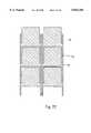
- FIG. 1shows a perspective view of a corner of the SLM device.
- FIGS. 2A-Gshow a basic fabrication process flow in cross-section.
- FIGS. 3A-Bshow in cross-section a single mirror modulating a light beam.
- FIG. 4shows the deflection angle of a mirror versus applied voltage bias.
- FIG. 5shows the electrical and mechanical torques acting on a deflectable mirror for several different voltage biases.
- FIG. 6shows a method by which the SLM pixels may be individually addressed using MOS transistors.
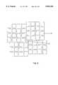
- FIGS. 7A-Cshow top view of mirror arrays with different hinge designs.
- FIG. 8shows spacer placement in a dense pixel array.
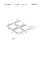
- FIG. 1A perspective view of a preferred embodiment of the spatial light modulator of this invention is shown in FIG. 1.
- Several rigid mirrors 48are attached to an optically transmissive substrate 20.
- the mirror 48 closest to the vieweris in the off or undeflected position, while the mirrors in the two adjacent positions are in their on or deflected states.
- the aperture layer between the mirrors and the optically transmissive substrateis not shown for clarity.
- FIGS. 2A-GThe fabrication process to produce the micro-mechanical spatial light modulator (SLM) of this invention is illustrated in cross-section in FIGS. 2A-G.
- the reflective deflecting elementsare rigid mirrors and are attached to the optically transmissive substrate 20.
- the substrate 20is made of which can withstand subsequent processing temperatures.
- a 50 nm thick layer of tungstenis deposited and patterned to form a light-blocking aperture layer 22.
- Tungstenis a refractory metal and remains stable during subsequent steps.
- a 200 nm protective layer 24 of LPCVD-grown silicon nitrideis deposited, as both an electrical insulator and an etch protection later.
- a 0.5 ⁇ m thick silicon dioxide sacrificial layer 26which will eventually be removed.
- a second low-stress silicon nitride mirror layer 28 of 150 nm thicknessis deposited.
- the deflectable mirrorsare created by patterning layer 28 as seen in FIG. 2B (a top view of this pattern can be seen in FIG. 8A).
- the sacrificial layer 26is partially removed in hydrofluoric acid (HF).
- HFhydrofluoric acid
- a photoresist layeris patterned to form small holds 30 as shown in FIG. 2C. The holds keep the mirrors immobile while all of the sacrificial layer 26 is removed via a second HF etch.
- the holdsprevent the mirror layer 28 from being pulled to the substrate 20 by capillary forces and also prevent the mirrors from being damaged during wet rinsing and drying.
- the holds 30are removed using an oxygen plasma dry etch. As seen in FIG. 2D, what remains after this etch are fully released mirrors 48.
- a thin 30 nm reflective layer 32 of aluminumis deposited on the entire mirror array. The aluminum also insures that all of the mirrors are electrically connected.
- the bottom circuit substrate 34 seen in FIG. 2Eis fabricated using standard VLSI techniques.
- An electrical schematic of one embodiment of the addressing circuitryis shown in FIG. 6. It resembles a standard memory array.
- a passivation later 38is deposited over the circuitry.
- a 0.5 ⁇ m aluminum layeris deposited and patterned to form bottom electrodes 42.
- Many configurationsare possible: what is important is that the active bottom electrode should be physically located higher than the rest of the circuit components and interconnects. This way the electrostatic interaction of the bottom electrode with the overhanging mirror will be the principle interaction with the mirror and the principle means of its deflection.
- a second passivation layer 46 of 0.5 ⁇ m thick silicon nitrideis deposited.
- a laminate of silicon dioxide (2.5 ⁇ m) topped by chromium (50 nm) and indium (200 nm)is deposited and patterned to form pillars 44 of fixed height.
- the finished circuit substrateis shown in FIG. 2F.
- the substratesare aligned optically and held together while heat is applied to melt the indium and form a seal.
- the finished deviceis seen in FIG. 2G. After cooling, the edges of the substrates can be glued and bond wires attached to make a very robust unit.
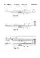
- FIGS. 3A-BThe operation of the above-described embodiment is shown in FIGS. 3A-B.
- the mirror 48In FIG. 3A the mirror 48 is undeflected. In this unbiased state, an incoming light beam perpendicularly incident to the modulator will pass through the optically transmissive substrate 20 and be reflected by the aperture layer 22 and the flat mirrors 48. The angle of the outgoing light beam 58 will then also be perpendicular to the optically transmissive substrate, within diffraction limits. Therefore, the modulator will behave optically as a perfect large pitch diffraction grating, which will diffract light only through a very small angle (about one degree for a 25 ⁇ m pitch grating), which is not sufficient to scatter any light into imaging optics.
- the incorporation of the aperture layer 22 into the optically transmissive substrateis a significant advantage of this modulator over the DMD and GLV: it simply and elegantly eliminates unwanted light scattering.
- the modulator with a voltage bias applied between the mirror 48 and the bottom electrode 42 appliedis shown in FIG. 3B.
- the mirroris deflected due to electrostatic attraction. Because of the design of the hinge, one end of the mirror will deflect towards the bottom silicon substrate. This will deflect the outgoing light beam 58 through a significant angle, and into the imaging optics.
- the snapping angledoes not depend significantly on the substrate-substrate separation and occurs when the mirror is approximately half-way deflected towards the lower substrate if the mechanical torque is linear in angle ⁇ .
- the modulatorIf the modulator is operated at voltages past the snapping point, it can be operated in a digital manner using either active addressing, with a transistor at each pixel location, or using passive addressing, by exploiting the electromechanical bistability. If the modulator is operated at voltages below the snapping point, it can operated in an analog fashion using active addressing. The mirror deflection will then be proportional to the charge stored at each coresponding electrode. Operation below the snapping point also has the advantage of preventing mechanical contact during operation, eliminating possible sticking problems. The use of high quality mechanical materials results in good uniformity over the pixel array, and makes analog operation practical.
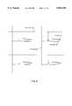
- an addressing scheme embodied in the circuitry of FIG. 6can be used.
- the substrates, and the mirror 48 and bottom electrode 42are drawn symbolically.
- the schemeis identical to that used for a DRAM (dynamic random access memory).
- Each pixelis driven by an NMOS transistor.
- the state of one row of pixelsis set by holding the bit lines 62 at the appropriate bias voltage for the desired mirror deflection.
- the biasis relative to the mirrors 48, which are connected to ground.
- the word line 60is then pulsed low-high-low and the voltage value is stored as charge between the bottom electrode 42 and mirror 48.
- An additional capacitormay have to be placed electrically in parallel to the mirror-electrode combination to insure that enough charge is stored to overcome leakage.
- a modulatorcan be made to have an operating voltage of only a few volts.
- the voltage at which the addressing circuitry must operatecan be made even lower by maintaining the mirror potential negative, as referenced to the circuit ground. This results in a larger difference in deflection angle for a given voltage difference.
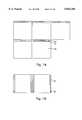
- FIG. 7AA top view of a section of the mirror array is presented in FIG. 7A.
- pillars 44may need to be embedded in the mirror array itself.
- FIG. 8A layout which accomplished this and maintains a reasonably contiguous SLM array is shown in FIG. 8.
- FIG. 7BOne simple variation is shown in FIG. 7B.
- the hingesoperate by flexion and not by torsion.
- This embodimentuses a single layer to form both the hinge and the mirror; a simple variation would be to deposit different layers for the hinge and the mirror plate itself.
- a thin torsion-type hingecould cross the plate, attaching to the plate only at one point.
- onecould thin an area of the mirror layer via an etch to form a thinner hinge, and thus lower switching voltages while keeping the plate rigid.
- a single square mirroris not the only possible reflective deflectable element possible; other designs, such as a cloverleaf or grating-like design are possible. For example, a row of skinny "mirrors" all deflecting in unison can form a switchable diffraction grating. It is even feasible that the reflective deflectable element is a metal-coated membrane. The deflectable element design could also be made so that one part of the element moves away from the lower substrate instead of towards it.
- additional structuremay be added.
- protruding bumpscan be fabricated to reduce the total surface area actually in contact.
- a conducting transparent layersuch as indium tin oxide, can be deposited before the protective layer 24. A bias applied between the conducting transparent layer and the mirrors will actively pull the mirrors to the top substrate 20 and reset them to their off state.
- a DRAM schemewas outlined above, but static RAM cells could also be used.
- a passive addressing schemecan be implemented that exploits the bistability inherent in this type of electromechanical device. Instead of all of the deflectable elements being electrically connected, addressing would be split between the bottom substrate where electrodes would run in one direction and the top substrate where the deflectable elements would be connected together in rows in a direction perpendicular to the columns. If voltage biases are applied to a row and a column, they would add only at one pixel, allowing it to be addressed individually. A large bias would turn on a pixel, a small bias would reset it, and an intermediate bias would leave the state of the deflectable elements unchanged. Even if an active addressing scheme is used, electrically connecting the deflecting elements of the top substrate in rows could increase addressing efficiency.
- the optically transmissive substratecontains an aperture layer in the shape of a grid. This layer may be further modified to comprise any binary optical pattern.
- the modulatorcould have more of a diffractive, as opposed to reflective, nature.
- other planar optical componentscan be integrated into the optically transmissive substrate, at either the top or bottom surface.
- Some of the many possible structuresinclude color filters composed of one or a stack of layers, micro-lenses, and color-dispersive or diffractive features. See for example Jahns and Huang, "Planar Integration of Free-Space Optical components" Applied Optics, vol. 28, No. 9, 1 May 1989.
- the ability to integrate this optical functionality into the optically transmissive substrateincreases achievable contrast ratio and lowers costs by reducing the cost of free-space optics at the systems level.
- the substratesmay be joined using a method very similar to that used in flat panel LCD manufacturing, which also requires sub-micron and micron vertical and lateral tolerances respectively.
- the substrateswill be optically aligned (to within 1-2 microns).
- the gap between the two substrateswould be partially evacuated, and the resulting pressure difference would push them together. They can then be bonded with adhesive along the edges.
- the pillars on one substratewill precisely control the separation distance. In any scheme, of course, the pillars can be built on either substrate. It is important to note that the method of deflection is also not necessarily restricted to electrostatic: thermal and piezo-electric actuation are among alternate possibilities.
- micro-mechanical elementsmany material substitutions are possible for the micro-mechanical elements: one possibility is the use of another type of ceramic (e.g. silicon dioxide) for the mirror, or even making the mirror completely out of a metal (e.g. an aluminum alloy).
- a metale.g. an aluminum alloy.
- the sacrificial layer materialsuch as silicon. Silicon could also be used instead of tungsten as the grid material. This would make the process more compatible with silicon nitride deposition facilities that are used for CMOS chip production.
- the pillarscan also be made from a wide variety of materials.
- the spatial light modulator of this inventionis a device that exhibits many desirable properties, including high resolution, high optical efficiency, high contrast ratio or modulation depth, and high mechanical reliability.
- the modulatorhas application in a wide variety of areas, including projection display systems.
- Low switching voltages and the innovative design of the modulatorenable standard VLSI circuitry to be used as the addressing mechanism. This makes the modulator easy and inexpensive to manufacture.
Landscapes
- Physics & Mathematics (AREA)
- General Physics & Mathematics (AREA)
- Optics & Photonics (AREA)
- Mechanical Light Control Or Optical Switches (AREA)
Abstract
Description
______________________________________ REFERENCE NUMERALS IN THE DRAWINGS ______________________________________ 20 Opticallytransmissive substrate 22Aperture layer 24Protective layer 25Via 26Sacrificial layer 28Mirror layer 30 Photoresist hold 32Reflective layer 34Circuit substrate 36Address circuit line 38 Passivation layer 40Via 42Bottom electrode 44Pillar 46Passivation layer 48Mirror 50Hinge 54Attachment region 56Incoming light beam 58Outgoing light beam 60Word line 62 Bitline ______________________________________
Claims (19)
Priority Applications (16)
| Application Number | Priority Date | Filing Date | Title |
|---|---|---|---|
| US08/665,380US5835256A (en) | 1995-06-19 | 1996-06-18 | Reflective spatial light modulator with encapsulated micro-mechanical elements |
| US09/160,361US6046840A (en) | 1995-06-19 | 1998-09-24 | Double substrate reflective spatial light modulator with self-limiting micro-mechanical elements |
| US09/437,586US6172797B1 (en) | 1995-06-19 | 1999-11-09 | Double substrate reflective spatial light modulator with self-limiting micro-mechanical elements |
| US09/624,591US6356378B1 (en) | 1995-06-19 | 2000-07-24 | Double substrate reflective spatial light modulator |
| US10/043,703US6538800B2 (en) | 1995-06-19 | 2002-01-09 | Reflective spatial light modulator with deflectable elements formed on a light transmissive substrate |
| US10/153,138US6690502B2 (en) | 1995-06-19 | 2002-05-20 | Double substrate reflective spatial light modulator with self-limiting micro-mechanical elements |
| US10/305,631US6952301B2 (en) | 1995-06-19 | 2002-11-26 | Spatial light modulators with light blocking and absorbing areas |
| US10/748,899US6798561B2 (en) | 1995-06-19 | 2003-12-29 | Double substrate reflective spatial light modulator with self-limiting micro-mechanical elements |
| US10/948,871US6947200B2 (en) | 1995-06-19 | 2004-09-24 | Double substrate reflective spatial light modulator with self-limiting micro-mechanical elements |
| US10/969,380US7138693B2 (en) | 1995-06-19 | 2004-10-19 | Barrier layers for microelectromechanical systems |
| US11/001,806US7023607B2 (en) | 1995-06-19 | 2004-12-01 | Double substrate reflective spatial light modulator with self-limiting micro-mechanical elements |
| US11/001,807US7012733B2 (en) | 1995-06-19 | 2004-12-01 | Double substrate reflective spatial light modulator with self-limiting micro-mechanical elements |
| US11/090,800US7009754B2 (en) | 1995-06-19 | 2005-03-24 | Double substrate reflective spatial light modulator with self-limiting micro-mechanical elements |
| US11/089,920US7027207B2 (en) | 1995-06-19 | 2005-03-24 | Double substrate reflective spatial light modulator with self-limiting micro-mechanical elements |
| US11/089,692US6975444B2 (en) | 1995-06-19 | 2005-03-24 | Double substrate reflective spatial light modulator with self-limiting micro-mechanical elements |
| US11/340,319US7403324B2 (en) | 1995-06-19 | 2006-01-25 | Double substrate reflective spatial light modulator with self-limiting micro-mechanical elements |
Applications Claiming Priority (2)
| Application Number | Priority Date | Filing Date | Title |
|---|---|---|---|
| US32295P | 1995-06-19 | 1995-06-19 | |
| US08/665,380US5835256A (en) | 1995-06-19 | 1996-06-18 | Reflective spatial light modulator with encapsulated micro-mechanical elements |
Related Child Applications (2)
| Application Number | Title | Priority Date | Filing Date |
|---|---|---|---|
| US09/160,361Continuation-In-PartUS6046840A (en) | 1995-06-19 | 1998-09-24 | Double substrate reflective spatial light modulator with self-limiting micro-mechanical elements |
| US09/160,361ContinuationUS6046840A (en) | 1995-06-19 | 1998-09-24 | Double substrate reflective spatial light modulator with self-limiting micro-mechanical elements |
Publications (1)
| Publication Number | Publication Date |
|---|---|
| US5835256Atrue US5835256A (en) | 1998-11-10 |
Family
ID=26667491
Family Applications (1)
| Application Number | Title | Priority Date | Filing Date |
|---|---|---|---|
| US08/665,380Expired - Fee RelatedUS5835256A (en) | 1995-06-19 | 1996-06-18 | Reflective spatial light modulator with encapsulated micro-mechanical elements |
Country Status (1)
| Country | Link |
|---|---|
| US (1) | US5835256A (en) |
Cited By (295)
| Publication number | Priority date | Publication date | Assignee | Title |
|---|---|---|---|---|
| US5999306A (en)* | 1995-12-01 | 1999-12-07 | Seiko Epson Corporation | Method of manufacturing spatial light modulator and electronic device employing it |
| US6031656A (en)* | 1998-10-28 | 2000-02-29 | Memsolutions, Inc. | Beam-addressed micromirror direct view display |
| US6034807A (en)* | 1998-10-28 | 2000-03-07 | Memsolutions, Inc. | Bistable paper white direct view display |
| US6052217A (en)* | 1997-06-30 | 2000-04-18 | Daewoo Electronics Co. Ltd. | Thin film actuated mirror array and method for manufacturing the same |
| WO2000077877A1 (en)* | 1999-06-11 | 2000-12-21 | University Of Hawaii | Mems transmission and circuit components |
| US6172797B1 (en) | 1995-06-19 | 2001-01-09 | Reflectivity, Inc. | Double substrate reflective spatial light modulator with self-limiting micro-mechanical elements |
| US6201629B1 (en)* | 1997-08-27 | 2001-03-13 | Microoptical Corporation | Torsional micro-mechanical mirror system |
| WO2001055769A1 (en)* | 2000-01-28 | 2001-08-02 | Reflectivity, Inc. | A deflectable spatial light modulator having superimposed hinge and deflectable element |
| WO2001056066A1 (en)* | 2000-01-28 | 2001-08-02 | Reflectivity, Inc. | A method for forming a micromechanical device |
| US6271957B1 (en)* | 1998-05-29 | 2001-08-07 | Affymetrix, Inc. | Methods involving direct write optical lithography |
| US6288821B1 (en) | 1999-10-01 | 2001-09-11 | Lucent Technologies, Inc. | Hybrid electro-optic device with combined mirror arrays |
| US6290864B1 (en) | 1999-10-26 | 2001-09-18 | Reflectivity, Inc. | Fluoride gas etching of silicon with improved selectivity |
| US6337760B1 (en) | 2000-07-17 | 2002-01-08 | Reflectivity, Inc. | Encapsulated multi-directional light beam steering device |
| US6342960B1 (en)* | 1998-12-18 | 2002-01-29 | The Boeing Company | Wavelength division multiplex transmitter |
| US6373619B1 (en)* | 1998-03-02 | 2002-04-16 | Micronic Laser Systems Ab | Pattern generator with improved address resolution |
| US6388661B1 (en) | 2000-05-03 | 2002-05-14 | Reflectivity, Inc. | Monochrome and color digital display systems and methods |
| US6396619B1 (en) | 2000-01-28 | 2002-05-28 | Reflectivity, Inc. | Deflectable spatial light modulator having stopping mechanisms |
| WO2002059679A1 (en)* | 2001-01-25 | 2002-08-01 | Nayna Networks, Inc. | Integrated mirror array and circuit device |
| US20020121502A1 (en)* | 1999-10-26 | 2002-09-05 | Patel Satyadev R. | Method for achieving improved selectivity in an etching process |
| US6449079B1 (en)* | 1998-12-16 | 2002-09-10 | Robert Bosch Gmbh | Deflectable micro-mirror |
| US20020145134A1 (en)* | 2001-03-09 | 2002-10-10 | Tim Olding | Sol-gel derived resistive and conductive coating |
| US6480646B2 (en)* | 2000-05-12 | 2002-11-12 | New Jersey Institute Of Technology | Micro-mirror and actuator with extended travel range |
| US20020171778A1 (en)* | 2001-05-16 | 2002-11-21 | Hubby Laurence M. | Optical system for full color, video projector using single light valve with plural sub-pixel reflectors |
| US6498686B2 (en) | 2001-03-30 | 2002-12-24 | Hewlett-Packard Company | Single light valve projector with reduced sequential color artifacts |
| US20020195423A1 (en)* | 1999-10-26 | 2002-12-26 | Reflectivity, Inc. | Method for vapor phase etching of silicon |
| US6523961B2 (en) | 2000-08-30 | 2003-02-25 | Reflectivity, Inc. | Projection system and mirror elements for improved contrast ratio in spatial light modulators |
| US20030054588A1 (en)* | 2000-12-07 | 2003-03-20 | Reflectivity, Inc., A California Corporation | Methods for depositing, releasing and packaging micro-electromechanical devices on wafer substrates |
| US20030073302A1 (en)* | 2001-10-12 | 2003-04-17 | Reflectivity, Inc., A California Corporation | Methods for formation of air gap interconnects |
| WO2002037162A3 (en)* | 2000-10-31 | 2003-05-01 | 3M Innovative Properties Co | Gimbaled micro-mirror positionable by thermal actuators |
| US20030107794A1 (en)* | 2001-12-11 | 2003-06-12 | Siekkinen James W. | Micro mirror array |
| US20030128367A1 (en)* | 2001-12-07 | 2003-07-10 | Tobjorn Sandstrom | Alignment sensor |
| US20030138363A1 (en)* | 1998-02-11 | 2003-07-24 | The Regents Of The University Of Michigan | Device for chemical and biochemical reactions using photo-generated reagents |
| US20030175748A1 (en)* | 2000-09-27 | 2003-09-18 | Feder John N. | Novel human G-protein coupled receptor, HGPRBMY3, expressed highly in immune- and colon- related tissues |
| WO2003081315A1 (en)* | 2002-03-26 | 2003-10-02 | Dicon A/S | Micro light modulator arrangement |
| US6639572B1 (en) | 1998-10-28 | 2003-10-28 | Intel Corporation | Paper white direct view display |
| US20030214639A1 (en)* | 2000-08-03 | 2003-11-20 | Satyadev Patel | Micromirrors with OFF-angle electrodes and stops |
| US20030234994A1 (en)* | 2002-06-19 | 2003-12-25 | Pan Shaoher X. | Reflective spatial light modulator |
| US6671078B2 (en)* | 2001-05-23 | 2003-12-30 | Axsun Technologies, Inc. | Electrostatic zipper actuator optical beam switching system and method of operation |
| US20040004753A1 (en)* | 2002-06-19 | 2004-01-08 | Pan Shaoher X. | Architecture of a reflective spatial light modulator |
| US20040012838A1 (en)* | 1995-06-19 | 2004-01-22 | Reflectivity, Inc., A California Corporation | Spatial light modulators with light blocking and absorbing areas |
| US20040035690A1 (en)* | 1998-02-11 | 2004-02-26 | The Regents Of The University Of Michigan | Method and apparatus for chemical and biochemical reactions using photo-generated reagents |
| US20040035821A1 (en)* | 1999-10-26 | 2004-02-26 | Doan Jonathan C. | Methods for forming and releasing microelectromechanical structures |
| US6704513B1 (en)* | 1998-12-21 | 2004-03-09 | Lucent Technologies, Inc. | Enhanced tilt optical power equalizer |
| US6707591B2 (en) | 2001-04-10 | 2004-03-16 | Silicon Light Machines | Angled illumination for a single order light modulator based projection system |
| US20040053143A1 (en)* | 2001-12-14 | 2004-03-18 | Micronic Laser Systems Ab | Methods and systems for improved boundary contrast |
| US6714337B1 (en) | 2002-06-28 | 2004-03-30 | Silicon Light Machines | Method and device for modulating a light beam and having an improved gamma response |
| US6712480B1 (en) | 2002-09-27 | 2004-03-30 | Silicon Light Machines | Controlled curvature of stressed micro-structures |
| US20040069742A1 (en)* | 2002-06-19 | 2004-04-15 | Pan Shaoher X. | Fabrication of a reflective spatial light modulator |
| US20040070040A1 (en)* | 2002-10-11 | 2004-04-15 | Aubuchon Christopher M. | Micromirror systems with side-supported mirrors and concealed flexure members |
| US20040070815A1 (en)* | 2002-10-11 | 2004-04-15 | Aubuchon Christopher M. | Micromirror systems with open support structures |
| US20040070813A1 (en)* | 2002-10-11 | 2004-04-15 | Aubuchon Christopher M. | Micromirror systems with electrodes configured for sequential mirror attraction |
| US6728023B1 (en) | 2002-05-28 | 2004-04-27 | Silicon Light Machines | Optical device arrays with optimized image resolution |
| US6741383B2 (en) | 2000-08-11 | 2004-05-25 | Reflectivity, Inc. | Deflectable micromirrors with stopping mechanisms |
| US20040100680A1 (en)* | 2002-11-26 | 2004-05-27 | Reflectivity, Inc., California Corporation | Spatial light modulators with light absorbing areas |
| US20040100677A1 (en)* | 2000-12-07 | 2004-05-27 | Reflectivity, Inc., A California Corporation | Spatial light modulators with light blocking/absorbing areas |
| US20040100594A1 (en)* | 2002-11-26 | 2004-05-27 | Reflectivity, Inc., A California Corporation | Spatial light modulators with light absorbing areas |
| US6747781B2 (en) | 2001-06-25 | 2004-06-08 | Silicon Light Machines, Inc. | Method, apparatus, and diffuser for reducing laser speckle |
| US6764875B2 (en) | 1998-07-29 | 2004-07-20 | Silicon Light Machines | Method of and apparatus for sealing an hermetic lid to a semiconductor die |
| US6767751B2 (en) | 2002-05-28 | 2004-07-27 | Silicon Light Machines, Inc. | Integrated driver process flow |
| US6771851B1 (en) | 2001-06-19 | 2004-08-03 | Nayna Networks | Fast switching method for a micro-mirror device for optical switching applications |
| US20040156090A1 (en)* | 2003-02-12 | 2004-08-12 | Patel Satyadev R. | High angle micro-mirrors and processes |
| US6782205B2 (en) | 2001-06-25 | 2004-08-24 | Silicon Light Machines | Method and apparatus for dynamic equalization in wavelength division multiplexing |
| US20040165249A1 (en)* | 2003-02-24 | 2004-08-26 | Aubuchon Christopher M. | Micromirror systems with concealed multi-piece hinge structures |
| US20040165250A1 (en)* | 2003-02-24 | 2004-08-26 | Aubuchon Christopher M. | Multi-tilt micromirror systems with concealed hinge structures |
| US6801354B1 (en) | 2002-08-20 | 2004-10-05 | Silicon Light Machines, Inc. | 2-D diffraction grating for substantially eliminating polarization dependent losses |
| US6800238B1 (en) | 2002-01-15 | 2004-10-05 | Silicon Light Machines, Inc. | Method for domain patterning in low coercive field ferroelectrics |
| US6806997B1 (en) | 2003-02-28 | 2004-10-19 | Silicon Light Machines, Inc. | Patterned diffractive light modulator ribbon for PDL reduction |
| US6813059B2 (en) | 2002-06-28 | 2004-11-02 | Silicon Light Machines, Inc. | Reduced formation of asperities in contact micro-structures |
| US20040223240A1 (en)* | 2000-08-30 | 2004-11-11 | Huibers Andrew G. | Micromirror array |
| US6822797B1 (en) | 2002-05-31 | 2004-11-23 | Silicon Light Machines, Inc. | Light modulator structure for producing high-contrast operation using zero-order light |
| US20040232535A1 (en)* | 2003-05-22 | 2004-11-25 | Terry Tarn | Microelectromechanical device packages with integral heaters |
| US20040240033A1 (en)* | 2002-06-19 | 2004-12-02 | Pan Shaoher X. | High fill ratio reflective spatial light modulator with hidden hinge |
| US6829077B1 (en) | 2003-02-28 | 2004-12-07 | Silicon Light Machines, Inc. | Diffractive light modulator with dynamically rotatable diffraction plane |
| US6829092B2 (en) | 2001-08-15 | 2004-12-07 | Silicon Light Machines, Inc. | Blazed grating light valve |
| US6829258B1 (en) | 2002-06-26 | 2004-12-07 | Silicon Light Machines, Inc. | Rapidly tunable external cavity laser |
| US20040251430A1 (en)* | 2003-06-12 | 2004-12-16 | Micronic Laser Systems Ab | Method for high precision printing of patterns |
| US20050007652A1 (en)* | 2003-07-10 | 2005-01-13 | Evans & Sutherland Computer Corporation. | Ultra-high resolution light modulation control system and method |
| US20050020089A1 (en)* | 2002-03-22 | 2005-01-27 | Hongqin Shi | Etching method used in fabrications of microstructures |
| US20050018091A1 (en)* | 2000-08-11 | 2005-01-27 | Patel Satyadev R. | Micromirror array device with a small pitch size |
| US6849471B2 (en) | 2003-03-28 | 2005-02-01 | Reflectivity, Inc. | Barrier layers for microelectromechanical systems |
| US6850353B1 (en) | 1999-06-11 | 2005-02-01 | University Of Hawaii | MEMS optical components |
| US20050024733A1 (en)* | 2003-07-25 | 2005-02-03 | Peter Richards | Color rendering of illumination light in display systems |
| US20050024734A1 (en)* | 2003-07-25 | 2005-02-03 | Peter Richards | Color rendering of illumination light in display systems |
| US20050032002A1 (en)* | 2003-08-04 | 2005-02-10 | Micronic Laser Systems Ab | Method to pattern a substrate |
| US6859299B1 (en) | 1999-06-11 | 2005-02-22 | Jung-Chih Chiao | MEMS optical components |
| US20050042792A1 (en)* | 2000-12-07 | 2005-02-24 | Patel Satyadev R. | Methods for depositing, releasing and packaging micro-electromechanical devices on wafer substrates |
| US6862127B1 (en) | 2003-11-01 | 2005-03-01 | Fusao Ishii | High performance micromirror arrays and methods of manufacturing the same |
| US20050045276A1 (en)* | 2001-05-22 | 2005-03-03 | Patel Satyadev R. | Method for making a micromechanical device by removing a sacrificial layer with multiple sequential etchants |
| US6865346B1 (en) | 2001-06-05 | 2005-03-08 | Silicon Light Machines Corporation | Fiber optic transceiver |
| US20050059254A1 (en)* | 2003-09-17 | 2005-03-17 | Hongqin Shi | Methods and apparatus of etch process control in fabrications of microstructures |
| US20050057792A1 (en)* | 2003-09-12 | 2005-03-17 | Shen-Ping Wang | Method of forming a micromechanical structure |
| US6872984B1 (en) | 1998-07-29 | 2005-03-29 | Silicon Light Machines Corporation | Method of sealing a hermetic lid to a semiconductor die at an angle |
| US20050074919A1 (en)* | 2000-12-07 | 2005-04-07 | Reflectivity, Inc. | Methods for depositing, releasing and packaging micro-electromechanical devices on wafer substrates |
| US20050088718A1 (en)* | 2003-07-03 | 2005-04-28 | Patel Satyadev R. | Micromirror array having reduced gap between adjacent micromirrors of the micromirror array |
| US20050088719A1 (en)* | 2003-07-03 | 2005-04-28 | Patel Satyadev R. | Micromirror having reduced space between hinge and mirror plate of the micromirror |
| US20050094240A1 (en)* | 2003-10-30 | 2005-05-05 | Andrew Huibers | Micromirror and post arrangements on substrates |
| US20050094242A1 (en)* | 2003-11-01 | 2005-05-05 | Fusao Ishii | Vacuum packaged micromirror arrays and methods of manufacturing the same |
| US20050094241A1 (en)* | 2003-11-01 | 2005-05-05 | Fusao Ishii | Electromechanical micromirror devices and methods of manufacturing the same |
| US20050093134A1 (en)* | 2003-10-30 | 2005-05-05 | Terry Tarn | Device packages with low stress assembly process |
| US6894836B2 (en) | 2001-08-28 | 2005-05-17 | Delphi Technologies, Inc. | Diffraction grating, method of making and method of using |
| US20050104144A1 (en)* | 2003-11-19 | 2005-05-19 | Xhp Microsystems, Inc. | Method and apparatus to reduce parasitic forces in electro-mechanical systems |
| US20050106774A1 (en)* | 2003-11-13 | 2005-05-19 | Dmitri Simonian | Surface processes in fabrications of microstructures |
| US6908201B2 (en) | 2002-06-28 | 2005-06-21 | Silicon Light Machines Corporation | Micro-support structures |
| US6913942B2 (en) | 2003-03-28 | 2005-07-05 | Reflectvity, Inc | Sacrificial layers for use in fabrications of microelectromechanical devices |
| EP1555563A2 (en) | 2000-08-03 | 2005-07-20 | Reflectivity Inc. | Color projection system |
| US20050157376A1 (en)* | 2002-11-26 | 2005-07-21 | Huibers Andrew G. | Spatial light modulators with light blocking/absorbing areas |
| US6922273B1 (en) | 2003-02-28 | 2005-07-26 | Silicon Light Machines Corporation | PDL mitigation structure for diffractive MEMS and gratings |
| US6922272B1 (en) | 2003-02-14 | 2005-07-26 | Silicon Light Machines Corporation | Method and apparatus for leveling thermal stress variations in multi-layer MEMS devices |
| US20050161432A1 (en)* | 2004-01-27 | 2005-07-28 | Jonathan Doan | Pre-oxidization of deformable elements of microstructures |
| US6928207B1 (en) | 2002-12-12 | 2005-08-09 | Silicon Light Machines Corporation | Apparatus for selectively blocking WDM channels |
| US6927891B1 (en) | 2002-12-23 | 2005-08-09 | Silicon Light Machines Corporation | Tilt-able grating plane for improved crosstalk in 1×N blaze switches |
| US20050174628A1 (en)* | 2002-06-19 | 2005-08-11 | Miradia Inc. | Memory cell dual protection |
| US6930364B2 (en) | 2001-09-13 | 2005-08-16 | Silicon Light Machines Corporation | Microelectronic mechanical system and methods |
| US6934070B1 (en) | 2002-12-18 | 2005-08-23 | Silicon Light Machines Corporation | Chirped optical MEM device |
| US20050190430A1 (en)* | 2000-08-11 | 2005-09-01 | Sataydev Patel | Micromirrors with mechanisms for enhancing coupling of the micromirrors with electrostatic fields |
| US20050196896A1 (en)* | 2003-05-13 | 2005-09-08 | Satyadev Patel | Micromirror array device |
| US20050200939A1 (en)* | 2004-03-10 | 2005-09-15 | Andrew Huibers | Micromirror modulation method and digital apparatus with improved grayscale |
| US6947613B1 (en) | 2003-02-11 | 2005-09-20 | Silicon Light Machines Corporation | Wavelength selective switch and equalizer |
| US6950223B2 (en)* | 2003-01-15 | 2005-09-27 | Reflectivity, Inc | Multiple hinge MEMS device |
| US6949202B1 (en) | 1999-10-26 | 2005-09-27 | Reflectivity, Inc | Apparatus and method for flow of process gas in an ultra-clean environment |
| US20050214970A1 (en)* | 2004-03-26 | 2005-09-29 | Jim Dunphy | Method and apparatus for lubricating microelectromechanical devices in packages |
| US20050212067A1 (en)* | 2004-03-26 | 2005-09-29 | Robert Duboc | Microelectromechanical devices with lubricants and getters formed thereon |
| US20050219502A1 (en)* | 2004-02-25 | 2005-10-06 | Micronic Laser Systems Ab | RET for optical maskless lithography |
| US20050225834A1 (en)* | 2004-04-02 | 2005-10-13 | Regan Michael J | Microelectromechanical device with reset electrode |
| US20050225832A1 (en)* | 2004-04-13 | 2005-10-13 | Jonathan Doan | Method of improving the performance of microstructures |
| US6956995B1 (en) | 2001-11-09 | 2005-10-18 | Silicon Light Machines Corporation | Optical communication arrangement |
| US6956878B1 (en) | 2000-02-07 | 2005-10-18 | Silicon Light Machines Corporation | Method and apparatus for reducing laser speckle using polarization averaging |
| US6962419B2 (en) | 1998-09-24 | 2005-11-08 | Reflectivity, Inc | Micromirror elements, package for the micromirror elements, and projection system therefor |
| US20050255666A1 (en)* | 2004-05-11 | 2005-11-17 | Miradia Inc. | Method and structure for aligning mechanical based device to integrated circuits |
| US20050270498A1 (en)* | 2004-06-04 | 2005-12-08 | Regis Grasser | Micromirror projection of polarized light |
| US20050275643A1 (en)* | 2004-06-11 | 2005-12-15 | Peter Richards | Asymmetrical switching delay compensation in display systems |
| US20050275930A1 (en)* | 2004-06-15 | 2005-12-15 | Satyadev Patel | Micromirror array assembly with in-array pillars |
| US6980349B1 (en) | 2004-08-25 | 2005-12-27 | Reflectivity, Inc | Micromirrors with novel mirror plates |
| US20050287694A1 (en)* | 2004-06-23 | 2005-12-29 | Rubinstein Y Dan | Wafer matching methods for use in assembling micromirror array devices |
| US20050286112A1 (en)* | 2004-06-23 | 2005-12-29 | Satyadev Patel | Micromirror having offset addressing electrode |
| US20060007515A1 (en)* | 2003-11-13 | 2006-01-12 | Dmitri Simonian | Surface lubrication in microstructures |
| US6987600B1 (en) | 2002-12-17 | 2006-01-17 | Silicon Light Machines Corporation | Arbitrary phase profile for better equalization in dynamic gain equalizer |
| US20060023286A1 (en)* | 2004-07-28 | 2006-02-02 | Miradia Inc. | Method and apparatus for a reflective spatial light modulator with a flexible pedestal |
| US20060035439A1 (en)* | 2004-08-13 | 2006-02-16 | Ching-Heng Po | Method of forming a micromechanical structure |
| US20060033977A1 (en)* | 2003-02-12 | 2006-02-16 | Patel Satyadev R | Micromirror device |
| US20060044519A1 (en)* | 2004-08-25 | 2006-03-02 | Andrew Huibers | Micromirrors and hinge structures for micromirror arrays in projection displays |
| US20060050353A1 (en)* | 2004-08-25 | 2006-03-09 | Andrew Huibers | Micromirrors and hinge structures for micromirror arrays in projection displays |
| US20060056005A1 (en)* | 2004-08-25 | 2006-03-16 | Satyadev Patel | Micromirror device and method for making the same |
| US7023606B2 (en) | 2001-08-03 | 2006-04-04 | Reflectivity, Inc | Micromirror array for projection TV |
| US7027202B1 (en) | 2003-02-28 | 2006-04-11 | Silicon Light Machines Corp | Silicon substrate as a light modulator sacrificial layer |
| US20060077123A1 (en)* | 2004-09-27 | 2006-04-13 | Gally Brian J | Optical films for controlling angular characteristics of displays |
| US20060077525A1 (en)* | 2004-10-19 | 2006-04-13 | Andrew Huibers | Micromirror array devices with light blocking areas |
| US20060082888A1 (en)* | 2004-10-19 | 2006-04-20 | Andrew Huibers | Optically reconfigurable light integrator in display systems using spatial light modulators |
| US20060082858A1 (en)* | 2004-10-19 | 2006-04-20 | Peter Heureux | Micromirror array device and a method for making the same |
| US7034984B2 (en) | 2002-06-19 | 2006-04-25 | Miradia Inc. | Fabrication of a high fill ratio reflective spatial light modulator with hidden hinge |
| US20060087717A1 (en)* | 2004-06-18 | 2006-04-27 | Miradia Inc. | Mirror structure with single crystal silicon cross-member |
| WO2005104717A3 (en)* | 2004-04-23 | 2006-04-27 | David E Dausch | Flexible electrostatic actuator |
| US20060093256A1 (en)* | 2004-10-29 | 2006-05-04 | Fujitsu Limited | Optical switch |
| US7042611B1 (en) | 2003-03-03 | 2006-05-09 | Silicon Light Machines Corporation | Pre-deflected bias ribbons |
| US7054515B1 (en) | 2002-05-30 | 2006-05-30 | Silicon Light Machines Corporation | Diffractive light modulator-based dynamic equalizer with integrated spectral monitor |
| US20060114214A1 (en)* | 2003-08-25 | 2006-06-01 | Dwight Griffin | Image rotation in display systems |
| US20060113639A1 (en)* | 2002-10-15 | 2006-06-01 | Sehat Sutardja | Integrated circuit including silicon wafer with annealed glass paste |
| US7057819B1 (en) | 2002-12-17 | 2006-06-06 | Silicon Light Machines Corporation | High contrast tilting ribbon blazed grating |
| US7057795B2 (en) | 2002-08-20 | 2006-06-06 | Silicon Light Machines Corporation | Micro-structures with individually addressable ribbon pairs |
| US7068372B1 (en) | 2003-01-28 | 2006-06-27 | Silicon Light Machines Corporation | MEMS interferometer-based reconfigurable optical add-and-drop multiplexor |
| US20060138076A1 (en)* | 2001-02-27 | 2006-06-29 | Philippe Robert | Method for making a planar suspended microstructure, using a sacrificial layer of polymer material and resulting component |
| US20060148121A1 (en)* | 2005-01-03 | 2006-07-06 | Miradia Inc. | Method and structure for forming an integrated spatial light modulator |
| US20060152794A1 (en)* | 2005-01-07 | 2006-07-13 | Miradia Inc. | Method and structure for reducing parasitic influences of deflection devices on spatial light modulators |
| US20060152795A1 (en)* | 2005-01-07 | 2006-07-13 | Miradia Inc. | Electrical contact method and structure for deflection devices formed in an array configuration |
| US20060220199A1 (en)* | 2005-04-05 | 2006-10-05 | Duboc Robert M | Low cost hermetically sealed package |
| US20060220045A1 (en)* | 2005-04-05 | 2006-10-05 | Jonathan Doan | Micromirror array device with compliant adhesive |
| US20060227406A1 (en)* | 2005-04-08 | 2006-10-12 | Satyadev Patel | Optical coating on light transmissive substrates of micromirror devices |
| US20060255457A1 (en)* | 2002-10-15 | 2006-11-16 | Sehat Sutardja | Integrated circuit package with glass layer and oscillator |
| US20060268388A1 (en)* | 1998-04-08 | 2006-11-30 | Miles Mark W | Movable micro-electromechanical device |
| US20060274397A1 (en)* | 2005-06-01 | 2006-12-07 | Miradia Inc. | Co-planar surface and torsion device mirror structure and method of manufacture for optical displays |
| US20060285192A1 (en)* | 2005-06-15 | 2006-12-21 | Miradia Inc. | Method and structure of patterning landing pad structures for spatial light modulators |
| US20060285083A1 (en)* | 2005-06-17 | 2006-12-21 | Andrew Huibers | Illumination system with integrated heat dissipation device for use in display systems employing spatial light modulators |
| US7177081B2 (en) | 2001-03-08 | 2007-02-13 | Silicon Light Machines Corporation | High contrast grating light valve type device |
| US7184195B2 (en) | 2005-06-15 | 2007-02-27 | Miradia Inc. | Method and structure reducing parasitic influences of deflection devices in an integrated spatial light modulator |
| US7189332B2 (en) | 2001-09-17 | 2007-03-13 | Texas Instruments Incorporated | Apparatus and method for detecting an endpoint in a vapor phase etch |
| US7202989B2 (en) | 2005-06-01 | 2007-04-10 | Miradia Inc. | Method and device for fabricating a release structure to facilitate bonding of mirror devices onto a substrate |
| US20070091483A1 (en)* | 2005-10-25 | 2007-04-26 | George Radominski | Display system |
| US20070176705A1 (en)* | 2002-10-15 | 2007-08-02 | Sehat Sutardja | Crystal oscillator emulator |
| US20070176690A1 (en)* | 2002-10-15 | 2007-08-02 | Sehat Sutardja | Crystal oscillator emulator |
| US20070188254A1 (en)* | 2002-10-15 | 2007-08-16 | Sehat Sutardja | Crystal oscillator emulator |
| US7274502B2 (en)* | 2004-12-22 | 2007-09-25 | Asml Holding N.V. | System, apparatus and method for maskless lithography that emulates binary, attenuating phase-shift and alternating phase-shift masks |
| US7286764B1 (en) | 2003-02-03 | 2007-10-23 | Silicon Light Machines Corporation | Reconfigurable modulator-based optical add-and-drop multiplexer |
| US20070258312A1 (en)* | 2006-05-05 | 2007-11-08 | Texas Instruments Incorporated | Memory Cell Array with Multiple Drivers |
| US7304784B2 (en) | 2004-09-27 | 2007-12-04 | Idc, Llc | Reflective display device having viewable display on both sides |
| US7321456B2 (en) | 2004-09-27 | 2008-01-22 | Idc, Llc | Method and device for corner interferometric modulation |
| US20080062500A1 (en)* | 2005-02-23 | 2008-03-13 | Pixtronix, Inc. | Methods and apparatus for spatial light modulation |
| EP1630781A3 (en)* | 2004-08-27 | 2008-04-16 | Idc, Llc | Method of sensing actuation and release voltages of an interferometric modulator comprising microelectromechanical systems (MEMS) and system for carrying out such a method |
| US7373026B2 (en) | 2004-09-27 | 2008-05-13 | Idc, Llc | MEMS device fabricated on a pre-patterned substrate |
| US20080130089A1 (en)* | 1994-05-05 | 2008-06-05 | Idc, Llc | METHOD OF FABRICATING MEMS DEVICES (SUCH AS IMod) COMPRISING USING A GAS PHASE ETCHANT TO REMOVE A LAYER |
| US7391973B1 (en) | 2003-02-28 | 2008-06-24 | Silicon Light Machines Corporation | Two-stage gain equalizer |
| US20080158635A1 (en)* | 2005-02-23 | 2008-07-03 | Pixtronix, Inc. | Display apparatus and methods for manufacture thereof |
| US7403180B1 (en) | 2007-01-29 | 2008-07-22 | Qualcomm Mems Technologies, Inc. | Hybrid color synthesis for multistate reflective modulator displays |
| US7405852B2 (en) | 2005-02-23 | 2008-07-29 | Pixtronix, Inc. | Display apparatus and methods for manufacture thereof |
| US7449284B2 (en) | 2004-05-11 | 2008-11-11 | Miradia Inc. | Method and structure for fabricating mechanical mirror structures using backside alignment techniques |
| US7450295B2 (en) | 2006-03-02 | 2008-11-11 | Qualcomm Mems Technologies, Inc. | Methods for producing MEMS with protective coatings using multi-component sacrificial layers |
| US7471444B2 (en) | 1996-12-19 | 2008-12-30 | Idc, Llc | Interferometric modulation of radiation |
| CN100451737C (en)* | 2004-04-23 | 2009-01-14 | 研究三角协会 | Flexible electrostatic actuator |
| US7502158B2 (en) | 2005-10-13 | 2009-03-10 | Miradia Inc. | Method and structure for high fill factor spatial light modulator with integrated spacer layer |
| US7511875B2 (en) | 1998-04-08 | 2009-03-31 | Idc, Llc | Moveable micro-electromechanical device |
| US7532386B2 (en) | 2004-09-27 | 2009-05-12 | Idc, Llc | Process for modifying offset voltage characteristics of an interferometric modulator |
| US7535621B2 (en) | 2006-12-27 | 2009-05-19 | Qualcomm Mems Technologies, Inc. | Aluminum fluoride films for microelectromechanical system applications |
| US7550794B2 (en) | 2002-09-20 | 2009-06-23 | Idc, Llc | Micromechanical systems device comprising a displaceable electrode and a charge-trapping layer |
| US7551344B2 (en) | 2005-02-23 | 2009-06-23 | Pixtronix, Inc. | Methods for manufacturing displays |
| US7564613B2 (en) | 2006-04-19 | 2009-07-21 | Qualcomm Mems Technologies, Inc. | Microelectromechanical device and method utilizing a porous surface |
| US7567373B2 (en) | 2004-07-29 | 2009-07-28 | Idc, Llc | System and method for micro-electromechanical operation of an interferometric modulator |
| US7566664B2 (en) | 2006-08-02 | 2009-07-28 | Qualcomm Mems Technologies, Inc. | Selective etching of MEMS using gaseous halides and reactive co-etchants |
| US20090190825A1 (en)* | 2004-06-23 | 2009-07-30 | Texas Instruments Incorporated | Performance Analyses of Micromirror Devices |
| US7570415B2 (en) | 2007-08-07 | 2009-08-04 | Qualcomm Mems Technologies, Inc. | MEMS device and interconnects for same |
| US20090201009A1 (en)* | 2008-02-11 | 2009-08-13 | Qualcomm Mems Technologies, Inc. | Methods for measurement and characterization of interferometric modulators |
| US20090201282A1 (en)* | 2008-02-11 | 2009-08-13 | Qualcomm Mems Technologies, Inc | Methods of tuning interferometric modulator displays |
| US20090201242A1 (en)* | 2008-02-11 | 2009-08-13 | Qualcomm Mems Technologies, Inc. | Sensing to determine pixel state in a passively addressed display array |
| US20090204350A1 (en)* | 2008-02-11 | 2009-08-13 | Qualcomms Technologies, Inc, | Methods for measurement and characterization of interferometric modulators |
| US7580172B2 (en) | 2005-09-30 | 2009-08-25 | Qualcomm Mems Technologies, Inc. | MEMS device and interconnects for same |
| US20090213450A1 (en)* | 2004-09-27 | 2009-08-27 | Idc, Llc | Support structures for electromechanical systems and methods of fabricating the same |
| US20090213107A1 (en)* | 2008-02-11 | 2009-08-27 | Qualcomm Mems Technologies, Inc, | Method and apparatus for sensing, measurement or characterization of display elements integrated with the display drive scheme, and system and applications using the same |
| US20090225396A1 (en)* | 2008-03-07 | 2009-09-10 | Qualcomm Mems Technologies, Inc. | System and methods for tiling display panels |
| US20090231673A1 (en)* | 2008-03-12 | 2009-09-17 | Texas Instruments Incorporated | Multilayered deformable element with reduced memory properties in a mems device |
| US20090231672A1 (en)* | 2008-03-12 | 2009-09-17 | Texas Instruments Incorporated | Electrically conductive protection layer and a microelectromechanical device using the same |
| US20090244678A1 (en)* | 2005-02-23 | 2009-10-01 | Pixtronix, Inc. | Display apparatus and methods for manufacture thereof |
| US20090303571A1 (en)* | 2008-04-24 | 2009-12-10 | Micronic Laser Systems Ab | Spatial Light Modulator with Structured Mirror Surfaces |
| US7636189B2 (en) | 2005-02-23 | 2009-12-22 | Pixtronix, Inc. | Display methods and apparatus |
| US20090323154A1 (en)* | 2008-06-25 | 2009-12-31 | Qualcomm Mems Technologies, Inc. | Backlight displays |
| US7643203B2 (en) | 2006-04-10 | 2010-01-05 | Qualcomm Mems Technologies, Inc. | Interferometric optical display system with broadband characteristics |
| US7652814B2 (en) | 2006-01-27 | 2010-01-26 | Qualcomm Mems Technologies, Inc. | MEMS device with integrated optical element |
| US20100027100A1 (en)* | 2008-08-04 | 2010-02-04 | Pixtronix, Inc. | Display with controlled formation of bubbles |
| US7660031B2 (en) | 2004-09-27 | 2010-02-09 | Qualcomm Mems Technologies, Inc. | Device and method for modifying actuation voltage thresholds of a deformable membrane in an interferometric modulator |
| US7660058B2 (en) | 2005-08-19 | 2010-02-09 | Qualcomm Mems Technologies, Inc. | Methods for etching layers within a MEMS device to achieve a tapered edge |
| US7688494B2 (en) | 2006-05-03 | 2010-03-30 | Qualcomm Mems Technologies, Inc. | Electrode and interconnect materials for MEMS devices |
| US20100109102A1 (en)* | 2005-01-03 | 2010-05-06 | Miradia Inc. | Method and structure for forming a gyroscope and accelerometer |
| US20100110518A1 (en)* | 2008-10-27 | 2010-05-06 | Pixtronix, Inc. | Mems anchors |
| US7719752B2 (en) | 2007-05-11 | 2010-05-18 | Qualcomm Mems Technologies, Inc. | MEMS structures, methods of fabricating MEMS components on separate substrates and assembly of same |
| US7733552B2 (en) | 2007-03-21 | 2010-06-08 | Qualcomm Mems Technologies, Inc | MEMS cavity-coating layers and methods |
| US7746529B2 (en) | 2005-02-23 | 2010-06-29 | Pixtronix, Inc. | MEMS display apparatus |
| US7755657B2 (en) | 2003-06-12 | 2010-07-13 | Micronic Laser Systems Ab | Method for high precision printing of patterns |
| US7755582B2 (en) | 2005-02-23 | 2010-07-13 | Pixtronix, Incorporated | Display methods and apparatus |
| DE102009000099A1 (en)* | 2009-01-09 | 2010-07-22 | Carl Zeiss Smt Ag | Micro mirror array with double bending beam arrangement and electronic actuators |
| US20100220248A1 (en)* | 1994-05-05 | 2010-09-02 | Qualcomm Mems Technologies, Inc. | Projection display |
| US7803536B2 (en) | 2002-09-20 | 2010-09-28 | Integrated Dna Technologies, Inc. | Methods of detecting fluorescence with anthraquinone quencher dyes |
| US20100245980A1 (en)* | 1996-11-05 | 2010-09-30 | Qualcomm Mems Technologies, Inc. | System and method for a mems device |
| US7808694B2 (en) | 1994-05-05 | 2010-10-05 | Qualcomm Mems Technologies, Inc. | Method and device for modulating light |
| US7807488B2 (en) | 2004-09-27 | 2010-10-05 | Qualcomm Mems Technologies, Inc. | Display element having filter material diffused in a substrate of the display element |
| US7808695B2 (en) | 2006-06-15 | 2010-10-05 | Qualcomm Mems Technologies, Inc. | Method and apparatus for low range bit depth enhancement for MEMS display architectures |
| US20100253925A1 (en)* | 2007-11-09 | 2010-10-07 | Nikon Corporation | Microactuator,optical device, display apparatus, exposure apparatus, and method for producing device |
| US7830588B2 (en) | 1996-12-19 | 2010-11-09 | Qualcomm Mems Technologies, Inc. | Method of making a light modulating display device and associated transistor circuitry and structures thereof |
| US7847999B2 (en) | 2007-09-14 | 2010-12-07 | Qualcomm Mems Technologies, Inc. | Interferometric modulator display devices |
| US7852545B2 (en) | 1994-05-05 | 2010-12-14 | Qualcomm Mems Technologies, Inc. | Method and device for modulating light |
| US7852546B2 (en) | 2007-10-19 | 2010-12-14 | Pixtronix, Inc. | Spacers for maintaining display apparatus alignment |
| US7852544B2 (en) | 1996-12-19 | 2010-12-14 | Qualcomm Mems Technologies, Inc. | Separable modulator |
| US7876489B2 (en) | 2006-06-05 | 2011-01-25 | Pixtronix, Inc. | Display apparatus with optical cavities |
| US7891818B2 (en) | 2006-12-12 | 2011-02-22 | Evans & Sutherland Computer Corporation | System and method for aligning RGB light in a single modulator projector |
| US7907319B2 (en) | 1995-11-06 | 2011-03-15 | Qualcomm Mems Technologies, Inc. | Method and device for modulating light with optical compensation |
| US7916378B2 (en) | 2007-03-08 | 2011-03-29 | Qualcomm Mems Technologies, Inc. | Method and apparatus for providing a light absorbing mask in an interferometric modulator display |
| US7969638B2 (en) | 2008-04-10 | 2011-06-28 | Qualcomm Mems Technologies, Inc. | Device having thin black mask and method of fabricating the same |
| US8040588B2 (en) | 2004-09-27 | 2011-10-18 | Qualcomm Mems Technologies, Inc. | System and method of illuminating interferometric modulators using backlighting |
| US8077378B1 (en) | 2008-11-12 | 2011-12-13 | Evans & Sutherland Computer Corporation | Calibration system and method for light modulation device |
| US8159428B2 (en) | 2005-02-23 | 2012-04-17 | Pixtronix, Inc. | Display methods and apparatus |
| KR101149860B1 (en) | 2004-02-03 | 2012-05-24 | 퀄컴 엠이엠에스 테크놀로지스, 인크. | Spatial light modulator with integrated optical structure |
| US8248560B2 (en) | 2008-04-18 | 2012-08-21 | Pixtronix, Inc. | Light guides and backlight systems incorporating prismatic structures and light redirectors |
| US8262274B2 (en) | 2006-10-20 | 2012-09-11 | Pitronix, Inc. | Light guides and backlight systems incorporating light redirectors at varying densities |
| US8310442B2 (en) | 2005-02-23 | 2012-11-13 | Pixtronix, Inc. | Circuits for controlling display apparatus |
| US8358317B2 (en) | 2008-05-23 | 2013-01-22 | Evans & Sutherland Computer Corporation | System and method for displaying a planar image on a curved surface |
| US8366867B2 (en) | 2007-06-25 | 2013-02-05 | Empire Technology Development Llc | Bonded structure, sealed structure, electronic component including the same, bonding method, and sealing method |
| US8416154B2 (en) | 2004-09-27 | 2013-04-09 | Qualcomm Mems Technologies, Inc. | Apparatus and method for reducing perceived color shift |
| US8482496B2 (en) | 2006-01-06 | 2013-07-09 | Pixtronix, Inc. | Circuits for controlling MEMS display apparatus on a transparent substrate |
| US8519945B2 (en) | 2006-01-06 | 2013-08-27 | Pixtronix, Inc. | Circuits for controlling display apparatus |
| US8520285B2 (en) | 2008-08-04 | 2013-08-27 | Pixtronix, Inc. | Methods for manufacturing cold seal fluid-filled display apparatus |
| US8526096B2 (en) | 2006-02-23 | 2013-09-03 | Pixtronix, Inc. | Mechanical light modulators with stressed beams |
| US8597460B2 (en) | 2007-05-30 | 2013-12-03 | Empire Technology Development Llc | Adhesion method, and biochemical chip and optical component made by the same |
| US8610986B2 (en) | 2009-04-06 | 2013-12-17 | The Board Of Trustees Of The University Of Illinois | Mirror arrays for maskless photolithography and image display |
| US8670171B2 (en) | 2010-10-18 | 2014-03-11 | Qualcomm Mems Technologies, Inc. | Display having an embedded microlens array |
| US8693084B2 (en) | 2008-03-07 | 2014-04-08 | Qualcomm Mems Technologies, Inc. | Interferometric modulator in transmission mode |
| US8702248B1 (en) | 2008-06-11 | 2014-04-22 | Evans & Sutherland Computer Corporation | Projection method for reducing interpixel gaps on a viewing surface |
| US8749538B2 (en) | 2011-10-21 | 2014-06-10 | Qualcomm Mems Technologies, Inc. | Device and method of controlling brightness of a display based on ambient lighting conditions |
| US8798425B2 (en) | 2007-12-07 | 2014-08-05 | Qualcomm Mems Technologies, Inc. | Decoupled holographic film and diffuser |
| US8848294B2 (en) | 2010-05-20 | 2014-09-30 | Qualcomm Mems Technologies, Inc. | Method and structure capable of changing color saturation |
| US8861071B2 (en) | 2004-09-27 | 2014-10-14 | Qualcomm Mems Technologies, Inc. | Method and device for compensating for color shift as a function of angle of view |
| US8872085B2 (en) | 2006-10-06 | 2014-10-28 | Qualcomm Mems Technologies, Inc. | Display device having front illuminator with turning features |
| US8928967B2 (en) | 1998-04-08 | 2015-01-06 | Qualcomm Mems Technologies, Inc. | Method and device for modulating light |
| US8971675B2 (en) | 2006-01-13 | 2015-03-03 | Qualcomm Mems Technologies, Inc. | Interconnect structure for MEMS device |
| US9019183B2 (en) | 2006-10-06 | 2015-04-28 | Qualcomm Mems Technologies, Inc. | Optical loss structure integrated in an illumination apparatus |
| US9025235B2 (en) | 2002-12-25 | 2015-05-05 | Qualcomm Mems Technologies, Inc. | Optical interference type of color display having optical diffusion layer between substrate and electrode |
| US9082353B2 (en) | 2010-01-05 | 2015-07-14 | Pixtronix, Inc. | Circuits for controlling display apparatus |
| US9087486B2 (en) | 2005-02-23 | 2015-07-21 | Pixtronix, Inc. | Circuits for controlling display apparatus |
| US9134552B2 (en) | 2013-03-13 | 2015-09-15 | Pixtronix, Inc. | Display apparatus with narrow gap electrostatic actuators |
| US9135868B2 (en) | 2005-02-23 | 2015-09-15 | Pixtronix, Inc. | Direct-view MEMS display devices and methods for generating images thereon |
| US9158106B2 (en) | 2005-02-23 | 2015-10-13 | Pixtronix, Inc. | Display methods and apparatus |
| US9170421B2 (en) | 2013-02-05 | 2015-10-27 | Pixtronix, Inc. | Display apparatus incorporating multi-level shutters |
| US9176318B2 (en) | 2007-05-18 | 2015-11-03 | Pixtronix, Inc. | Methods for manufacturing fluid-filled MEMS displays |
| US9183812B2 (en) | 2013-01-29 | 2015-11-10 | Pixtronix, Inc. | Ambient light aware display apparatus |
| US9229222B2 (en) | 2005-02-23 | 2016-01-05 | Pixtronix, Inc. | Alignment methods in fluid-filled MEMS displays |
| US9261694B2 (en) | 2005-02-23 | 2016-02-16 | Pixtronix, Inc. | Display apparatus and methods for manufacture thereof |
| US9291813B2 (en) | 2010-12-20 | 2016-03-22 | Pixtronix, Inc. | Systems and methods for MEMS light modulator arrays with reduced acoustic emission |
| US9398666B2 (en) | 2010-03-11 | 2016-07-19 | Pixtronix, Inc. | Reflective and transflective operation modes for a display device |
| US9641826B1 (en) | 2011-10-06 | 2017-05-02 | Evans & Sutherland Computer Corporation | System and method for displaying distant 3-D stereo on a dome surface |
| WO2023212173A3 (en)* | 2022-04-29 | 2024-04-04 | President And Fellows Of Harvard College | Systems and methods for retrieving cells from a continuous culture microfluidic device |
Citations (6)
| Publication number | Priority date | Publication date | Assignee | Title |
|---|---|---|---|---|
| US3746911A (en)* | 1971-04-13 | 1973-07-17 | Westinghouse Electric Corp | Electrostatically deflectable light valves for projection displays |
| US4229732A (en)* | 1978-12-11 | 1980-10-21 | International Business Machines Corporation | Micromechanical display logic and array |
| US5078479A (en)* | 1990-04-20 | 1992-01-07 | Centre Suisse D'electronique Et De Microtechnique Sa | Light modulation device with matrix addressing |
| US5216537A (en)* | 1990-06-29 | 1993-06-01 | Texas Instruments Incorporated | Architecture and process for integrating DMD with control circuit substrates |
| US5311360A (en)* | 1992-04-28 | 1994-05-10 | The Board Of Trustees Of The Leland Stanford, Junior University | Method and apparatus for modulating a light beam |
| US5535047A (en)* | 1995-04-18 | 1996-07-09 | Texas Instruments Incorporated | Active yoke hidden hinge digital micromirror device |
- 1996
- 1996-06-18USUS08/665,380patent/US5835256A/ennot_activeExpired - Fee Related
Patent Citations (6)
| Publication number | Priority date | Publication date | Assignee | Title |
|---|---|---|---|---|
| US3746911A (en)* | 1971-04-13 | 1973-07-17 | Westinghouse Electric Corp | Electrostatically deflectable light valves for projection displays |
| US4229732A (en)* | 1978-12-11 | 1980-10-21 | International Business Machines Corporation | Micromechanical display logic and array |
| US5078479A (en)* | 1990-04-20 | 1992-01-07 | Centre Suisse D'electronique Et De Microtechnique Sa | Light modulation device with matrix addressing |
| US5216537A (en)* | 1990-06-29 | 1993-06-01 | Texas Instruments Incorporated | Architecture and process for integrating DMD with control circuit substrates |
| US5311360A (en)* | 1992-04-28 | 1994-05-10 | The Board Of Trustees Of The Leland Stanford, Junior University | Method and apparatus for modulating a light beam |
| US5535047A (en)* | 1995-04-18 | 1996-07-09 | Texas Instruments Incorporated | Active yoke hidden hinge digital micromirror device |
Non-Patent Citations (12)
| Title |
|---|
| Cadman "New Micromechanical Display Using Thin Metallic Films" IEEE Electron Device Letters, Jan. 1983, pp.3-4, vEDL-4 n1, IEEE (U.S.A.). |
| Cadman New Micromechanical Display Using Thin Metallic Films IEEE Electron Device Letters, Jan. 1983, pp.3 4, vEDL 4 n1, IEEE (U.S.A.).* |
| Gerhard Multhaupt Light Valve Projection Displays an Introduction Displays, Jan. 1995, pp. 5 7, v16 n1, Elsevier Science, Holland.* |
| Gerhard Multhaupt Light Valve Technologies for High Definition Television Projection Displays Displays, 1991, pp. 115 128, v12 n3/4.* |
| Gerhard-Multhaupt "Light-Valve Projection Displays--an Introduction" Displays, Jan. 1995, pp. 5-7, v16 n1, Elsevier Science, Holland. |
| Gerhard-Multhaupt "Light-Valve Technologies for High-Definition Television Projection Displays" Displays, 1991, pp. 115-128, v12 n3/4. |
| Jaecklin "Line-Addressable Torsional Micromirrors for Light Modulator Arrays" Sensors & Actuators A, 1994, pp. 324-329, 441-442, Elsevier. |
| Jaecklin Line Addressable Torsional Micromirrors for Light Modulator Arrays Sensors & Actuators A, 1994, pp. 324 329, 441 442, Elsevier.* |
| K u ck Deformable Micromirror Devices as Phase Mod High Resolution Light Valves Transducers 95/Eurosensors IX, 29 Jun. 1995, Conf. Proceedings, Stockholm, Sweden.* |
| Kuck "Deformable Micromirror Devices as Phase-Mod High Resolution Light Valves" Transducers '95/Eurosensors IX, 29 Jun. 1995, Conf. Proceedings, Stockholm, Sweden. |
| Petersen "Micromechanical light modulator Array Fabricated on Silicon" Applied Physics Letters, 15 Oct. 1977, pp. 521-523, v31 n8, Amer. Inst. of Physics. |
| Petersen Micromechanical light modulator Array Fabricated on Silicon Applied Physics Letters, 15 Oct. 1977, pp. 521 523, v31 n8, Amer. Inst. of Physics.* |
Cited By (591)
| Publication number | Priority date | Publication date | Assignee | Title |
|---|---|---|---|---|
| US20080130089A1 (en)* | 1994-05-05 | 2008-06-05 | Idc, Llc | METHOD OF FABRICATING MEMS DEVICES (SUCH AS IMod) COMPRISING USING A GAS PHASE ETCHANT TO REMOVE A LAYER |
| US7808694B2 (en) | 1994-05-05 | 2010-10-05 | Qualcomm Mems Technologies, Inc. | Method and device for modulating light |
| US8105496B2 (en)* | 1994-05-05 | 2012-01-31 | Qualcomm Mems Technologies, Inc. | Method of fabricating MEMS devices (such as IMod) comprising using a gas phase etchant to remove a layer |
| US7852545B2 (en) | 1994-05-05 | 2010-12-14 | Qualcomm Mems Technologies, Inc. | Method and device for modulating light |
| US20100220248A1 (en)* | 1994-05-05 | 2010-09-02 | Qualcomm Mems Technologies, Inc. | Projection display |
| US6947200B2 (en) | 1995-06-19 | 2005-09-20 | Reflectivity, Inc | Double substrate reflective spatial light modulator with self-limiting micro-mechanical elements |
| US6690502B2 (en) | 1995-06-19 | 2004-02-10 | Reflectivity, Inc. | Double substrate reflective spatial light modulator with self-limiting micro-mechanical elements |
| US6952301B2 (en) | 1995-06-19 | 2005-10-04 | Reflectivity, Inc | Spatial light modulators with light blocking and absorbing areas |
| US7138693B2 (en) | 1995-06-19 | 2006-11-21 | Reflectivity, Inc. | Barrier layers for microelectromechanical systems |
| US20050041277A1 (en)* | 1995-06-19 | 2005-02-24 | Huibers Andrew G. | Double substrate reflective spatial light modulator with self-limiting micro-mechanical elements |
| US7012733B2 (en) | 1995-06-19 | 2006-03-14 | Reflectivity, Inc | Double substrate reflective spatial light modulator with self-limiting micro-mechanical elements |
| US7009754B2 (en) | 1995-06-19 | 2006-03-07 | Reflectivity, Inc | Double substrate reflective spatial light modulator with self-limiting micro-mechanical elements |
| US20050054135A1 (en)* | 1995-06-19 | 2005-03-10 | Satyadev Patel | Barrier layers for microelectromechanical systems |
| US7023607B2 (en) | 1995-06-19 | 2006-04-04 | Reflectivity, Inc | Double substrate reflective spatial light modulator with self-limiting micro-mechanical elements |
| US20050168795A1 (en)* | 1995-06-19 | 2005-08-04 | Huibers Andrew G. | Double substrate reflective spatial light modulator with self-limiting micro-mechanical elements |
| US7403324B2 (en) | 1995-06-19 | 2008-07-22 | Texas Instruments Incorporated | Double substrate reflective spatial light modulator with self-limiting micro-mechanical elements |
| US6172797B1 (en) | 1995-06-19 | 2001-01-09 | Reflectivity, Inc. | Double substrate reflective spatial light modulator with self-limiting micro-mechanical elements |
| US6356378B1 (en) | 1995-06-19 | 2002-03-12 | Reflectivity, Inc. | Double substrate reflective spatial light modulator |
| US7027207B2 (en) | 1995-06-19 | 2006-04-11 | Reflectivity, Inc | Double substrate reflective spatial light modulator with self-limiting micro-mechanical elements |
| US20040012838A1 (en)* | 1995-06-19 | 2004-01-22 | Reflectivity, Inc., A California Corporation | Spatial light modulators with light blocking and absorbing areas |
| US20040141224A1 (en)* | 1995-06-19 | 2004-07-22 | Huibers Andrew G. | Double substrate reflective spatial light modulator with self-limiting micro-mechanical elements |
| US6975444B2 (en) | 1995-06-19 | 2005-12-13 | Reflectivity, Inc. | Double substrate reflective spatial light modulator with self-limiting micro-mechanical elements |
| US20060132892A1 (en)* | 1995-06-19 | 2006-06-22 | Huibers Andrew G | Double substrate reflective spatial light modulator with self-limiting micro-mechanical elements |
| US6538800B2 (en) | 1995-06-19 | 2003-03-25 | Reflectivity, Inc. | Reflective spatial light modulator with deflectable elements formed on a light transmissive substrate |
| US20050174626A1 (en)* | 1995-06-19 | 2005-08-11 | Huibers Andrew G. | Double substrate reflective spatial light modulator with self-limiting micro-mechanical elements |
| US6798561B2 (en) | 1995-06-19 | 2004-09-28 | Reflectivity, Inc | Double substrate reflective spatial light modulator with self-limiting micro-mechanical elements |
| US20050105160A1 (en)* | 1995-06-19 | 2005-05-19 | Huibers Andrew G. | Double substrate reflective spatial light modulator with self-limiting micro-mechanical elements |
| US20050174625A1 (en)* | 1995-06-19 | 2005-08-11 | Huibers Andrew G. | Double substrate reflective spatial light modulator with self-limiting micro-mechanical elements |
| US7907319B2 (en) | 1995-11-06 | 2011-03-15 | Qualcomm Mems Technologies, Inc. | Method and device for modulating light with optical compensation |
| US6650461B2 (en) | 1995-12-01 | 2003-11-18 | Seiko Epson Corporation | Method of manufacturing spatial light modulator and electronic device employing it |
| US6271955B1 (en) | 1995-12-01 | 2001-08-07 | Seiko Epson Corporation | Method of manufacturing spatial light modulator and electronic device employing it |
| US6107115A (en)* | 1995-12-01 | 2000-08-22 | Seiko Epson Corporation | Method of manufacturing spatial light modulator and electronic device employing it |
| US5999306A (en)* | 1995-12-01 | 1999-12-07 | Seiko Epson Corporation | Method of manufacturing spatial light modulator and electronic device employing it |
| US6452712B2 (en) | 1995-12-01 | 2002-09-17 | Seiko Epson Corporation | Method of manufacturing spatial light modulator and electronic device employing it |
| US20100245980A1 (en)* | 1996-11-05 | 2010-09-30 | Qualcomm Mems Technologies, Inc. | System and method for a mems device |
| US7929197B2 (en) | 1996-11-05 | 2011-04-19 | Qualcomm Mems Technologies, Inc. | System and method for a MEMS device |
| US7830588B2 (en) | 1996-12-19 | 2010-11-09 | Qualcomm Mems Technologies, Inc. | Method of making a light modulating display device and associated transistor circuitry and structures thereof |
| US7852544B2 (en) | 1996-12-19 | 2010-12-14 | Qualcomm Mems Technologies, Inc. | Separable modulator |
| US7471444B2 (en) | 1996-12-19 | 2008-12-30 | Idc, Llc | Interferometric modulation of radiation |
| US6052217A (en)* | 1997-06-30 | 2000-04-18 | Daewoo Electronics Co. Ltd. | Thin film actuated mirror array and method for manufacturing the same |
| US6201629B1 (en)* | 1997-08-27 | 2001-03-13 | Microoptical Corporation | Torsional micro-mechanical mirror system |
| US6353492B2 (en) | 1997-08-27 | 2002-03-05 | The Microoptical Corporation | Method of fabrication of a torsional micro-mechanical mirror system |
| US6538799B2 (en) | 1997-08-27 | 2003-03-25 | The Microoptical Corporation | Magnetically actuated torsional micro-mechanical mirror system |
| US20080318806A1 (en)* | 1998-02-11 | 2008-12-25 | The Regents Of The University Of Michigan | Device for chemical and biochemical reactions using photo-generated reagents |
| US20030186427A1 (en)* | 1998-02-11 | 2003-10-02 | The Regents Of The University Of Michigan | Device for chemical and biochemical reactions using photo-generated reagents |
| US20030143131A1 (en)* | 1998-02-11 | 2003-07-31 | The Regents Of The University Of Michigan | Device for chemical and biochemical reactions using photo-generated reagents |
| US20030138363A1 (en)* | 1998-02-11 | 2003-07-24 | The Regents Of The University Of Michigan | Device for chemical and biochemical reactions using photo-generated reagents |
| US20040023368A1 (en)* | 1998-02-11 | 2004-02-05 | The Regents Of The University Of Michigan | Device for chemical and biochemical reactions using photo-generated reagents |
| US20110170075A1 (en)* | 1998-02-11 | 2011-07-14 | Xiaolian Gao | Device for chemical and biochemical reactions using photo-generated reagents |
| US20040035690A1 (en)* | 1998-02-11 | 2004-02-26 | The Regents Of The University Of Michigan | Method and apparatus for chemical and biochemical reactions using photo-generated reagents |
| US7838466B2 (en) | 1998-02-11 | 2010-11-23 | The Regents Of The University Of Michigan | Device for chemical and biochemical reactions using photo-generated reagents |
| US7491680B2 (en) | 1998-02-11 | 2009-02-17 | The Regents Of The University Of Michigan | Device for chemical and biochemical reactions using photo-generated reagents |
| US7544638B2 (en) | 1998-02-11 | 2009-06-09 | The Regents Of The University Of Michigan | Device for chemical and biochemical reactions using photo-generated reagents |
| US20100208327A1 (en)* | 1998-03-02 | 2010-08-19 | Torbjorn Sandstrom | Pattern generator |
| US20090191489A1 (en)* | 1998-03-02 | 2009-07-30 | Torbjorn Sandstrom | Pattern generator |
| US6987599B2 (en) | 1998-03-02 | 2006-01-17 | Micronic Laser Systems Ab | Pattern generator mirror configurations |
| US6373619B1 (en)* | 1998-03-02 | 2002-04-16 | Micronic Laser Systems Ab | Pattern generator with improved address resolution |
| US20060103914A1 (en)* | 1998-03-02 | 2006-05-18 | Torbjorn Sandstrom | Pattern generator |
| US7800815B2 (en) | 1998-03-02 | 2010-09-21 | Micronic Laser Systems Ab | Pattern generator |
| US7957055B2 (en) | 1998-03-02 | 2011-06-07 | Micronic Mydata AB | Pattern generator |
| US6747783B1 (en) | 1998-03-02 | 2004-06-08 | Micronic Laser Systems Ab | Pattern generator |
| US7365901B2 (en) | 1998-03-02 | 2008-04-29 | Micronic Laser Systems Ab | Pattern generator |
| US7710634B2 (en) | 1998-03-02 | 2010-05-04 | Micronic Laser Systems Ab | Pattern generator |
| US20080079922A1 (en)* | 1998-03-02 | 2008-04-03 | Torbjorn Sandstrom | Pattern generator |
| US7787174B2 (en) | 1998-03-02 | 2010-08-31 | Micronic Laser Systems Ab | Pattern generator |
| US7009753B2 (en) | 1998-03-02 | 2006-03-07 | Micronic Laser Systems Ab | Pattern generator |
| US8928967B2 (en) | 1998-04-08 | 2015-01-06 | Qualcomm Mems Technologies, Inc. | Method and device for modulating light |
| US7532377B2 (en) | 1998-04-08 | 2009-05-12 | Idc, Llc | Movable micro-electromechanical device |
| US20090135463A1 (en)* | 1998-04-08 | 2009-05-28 | Idc, Llc | Moveable micro-electromechanical device |
| US7554711B2 (en)* | 1998-04-08 | 2009-06-30 | Idc, Llc. | MEMS devices with stiction bumps |
| US9110289B2 (en) | 1998-04-08 | 2015-08-18 | Qualcomm Mems Technologies, Inc. | Device for modulating light with multiple electrodes |
| US7872792B2 (en) | 1998-04-08 | 2011-01-18 | Qualcomm Mems Technologies, Inc. | Method and device for modulating light with multiple electrodes |
| US20060268388A1 (en)* | 1998-04-08 | 2006-11-30 | Miles Mark W | Movable micro-electromechanical device |
| US7791787B2 (en) | 1998-04-08 | 2010-09-07 | Qualcomm Mems Technologies, Inc. | Moveable micro-electromechanical device |
| US7511875B2 (en) | 1998-04-08 | 2009-03-31 | Idc, Llc | Moveable micro-electromechanical device |
| US6271957B1 (en)* | 1998-05-29 | 2001-08-07 | Affymetrix, Inc. | Methods involving direct write optical lithography |
| US20050088722A1 (en)* | 1998-05-29 | 2005-04-28 | Affymetrix, Inc. | Compositions and methods involving direct write optical lithography |
| US20050233256A1 (en)* | 1998-05-29 | 2005-10-20 | Affymetrix, Inc., A California Corporation | Compositions and methods involving direct write optical lithography |
| US20060292628A1 (en)* | 1998-05-29 | 2006-12-28 | Affymetrix, Inc. | Compositions and methods involving direct write optical lithography |
| US6480324B2 (en) | 1998-05-29 | 2002-11-12 | Affymetrix, Inc. | Methods involving direct write optical lithography |
| US6764875B2 (en) | 1998-07-29 | 2004-07-20 | Silicon Light Machines | Method of and apparatus for sealing an hermetic lid to a semiconductor die |
| US6872984B1 (en) | 1998-07-29 | 2005-03-29 | Silicon Light Machines Corporation | Method of sealing a hermetic lid to a semiconductor die at an angle |
| US6962419B2 (en) | 1998-09-24 | 2005-11-08 | Reflectivity, Inc | Micromirror elements, package for the micromirror elements, and projection system therefor |
| US6529310B1 (en) | 1998-09-24 | 2003-03-04 | Reflectivity, Inc. | Deflectable spatial light modulator having superimposed hinge and deflectable element |
| US6034807A (en)* | 1998-10-28 | 2000-03-07 | Memsolutions, Inc. | Bistable paper white direct view display |
| US6639572B1 (en) | 1998-10-28 | 2003-10-28 | Intel Corporation | Paper white direct view display |
| US6031656A (en)* | 1998-10-28 | 2000-02-29 | Memsolutions, Inc. | Beam-addressed micromirror direct view display |
| US6449079B1 (en)* | 1998-12-16 | 2002-09-10 | Robert Bosch Gmbh | Deflectable micro-mirror |
| US6342960B1 (en)* | 1998-12-18 | 2002-01-29 | The Boeing Company | Wavelength division multiplex transmitter |
| US6704513B1 (en)* | 1998-12-21 | 2004-03-09 | Lucent Technologies, Inc. | Enhanced tilt optical power equalizer |
| US6850353B1 (en) | 1999-06-11 | 2005-02-01 | University Of Hawaii | MEMS optical components |
| US6859299B1 (en) | 1999-06-11 | 2005-02-22 | Jung-Chih Chiao | MEMS optical components |
| WO2000077877A1 (en)* | 1999-06-11 | 2000-12-21 | University Of Hawaii | Mems transmission and circuit components |
| US6288821B1 (en) | 1999-10-01 | 2001-09-11 | Lucent Technologies, Inc. | Hybrid electro-optic device with combined mirror arrays |
| US6942811B2 (en) | 1999-10-26 | 2005-09-13 | Reflectivity, Inc | Method for achieving improved selectivity in an etching process |
| US7041224B2 (en) | 1999-10-26 | 2006-05-09 | Reflectivity, Inc. | Method for vapor phase etching of silicon |
| US6960305B2 (en) | 1999-10-26 | 2005-11-01 | Reflectivity, Inc | Methods for forming and releasing microelectromechanical structures |
| US20020195423A1 (en)* | 1999-10-26 | 2002-12-26 | Reflectivity, Inc. | Method for vapor phase etching of silicon |
| US20020121502A1 (en)* | 1999-10-26 | 2002-09-05 | Patel Satyadev R. | Method for achieving improved selectivity in an etching process |
| US20040035821A1 (en)* | 1999-10-26 | 2004-02-26 | Doan Jonathan C. | Methods for forming and releasing microelectromechanical structures |
| US6290864B1 (en) | 1999-10-26 | 2001-09-18 | Reflectivity, Inc. | Fluoride gas etching of silicon with improved selectivity |
| US6949202B1 (en) | 1999-10-26 | 2005-09-27 | Reflectivity, Inc | Apparatus and method for flow of process gas in an ultra-clean environment |
| WO2001055769A1 (en)* | 2000-01-28 | 2001-08-02 | Reflectivity, Inc. | A deflectable spatial light modulator having superimposed hinge and deflectable element |
| WO2001056066A1 (en)* | 2000-01-28 | 2001-08-02 | Reflectivity, Inc. | A method for forming a micromechanical device |
| US6396619B1 (en) | 2000-01-28 | 2002-05-28 | Reflectivity, Inc. | Deflectable spatial light modulator having stopping mechanisms |
| US6956878B1 (en) | 2000-02-07 | 2005-10-18 | Silicon Light Machines Corporation | Method and apparatus for reducing laser speckle using polarization averaging |
| US6388661B1 (en) | 2000-05-03 | 2002-05-14 | Reflectivity, Inc. | Monochrome and color digital display systems and methods |
| US6756976B2 (en) | 2000-05-03 | 2004-06-29 | Reflectivity, Inc | Monochrome and color digital display systems and methods for implementing the same |
| US6480646B2 (en)* | 2000-05-12 | 2002-11-12 | New Jersey Institute Of Technology | Micro-mirror and actuator with extended travel range |
| US6337760B1 (en) | 2000-07-17 | 2002-01-08 | Reflectivity, Inc. | Encapsulated multi-directional light beam steering device |
| US6525864B1 (en)* | 2000-07-20 | 2003-02-25 | Nayna Networks, Inc. | Integrated mirror array and circuit device |
| EP1555563A2 (en) | 2000-08-03 | 2005-07-20 | Reflectivity Inc. | Color projection system |
| US20030214639A1 (en)* | 2000-08-03 | 2003-11-20 | Satyadev Patel | Micromirrors with OFF-angle electrodes and stops |
| US7099065B2 (en) | 2000-08-03 | 2006-08-29 | Reflectivity, Inc. | Micromirrors with OFF-angle electrodes and stops |
| US20050190430A1 (en)* | 2000-08-11 | 2005-09-01 | Sataydev Patel | Micromirrors with mechanisms for enhancing coupling of the micromirrors with electrostatic fields |
| US20050018091A1 (en)* | 2000-08-11 | 2005-01-27 | Patel Satyadev R. | Micromirror array device with a small pitch size |
| US6741383B2 (en) | 2000-08-11 | 2004-05-25 | Reflectivity, Inc. | Deflectable micromirrors with stopping mechanisms |
| US7019376B2 (en) | 2000-08-11 | 2006-03-28 | Reflectivity, Inc | Micromirror array device with a small pitch size |
| US6974713B2 (en) | 2000-08-11 | 2005-12-13 | Reflectivity, Inc. | Micromirrors with mechanisms for enhancing coupling of the micromirrors with electrostatic fields |
| US7012731B2 (en) | 2000-08-30 | 2006-03-14 | Reflectivity, Inc | Packaged micromirror array for a projection display |
| US7196740B2 (en) | 2000-08-30 | 2007-03-27 | Texas Instruments Incorporated | Projection TV with improved micromirror array |
| US7006275B2 (en) | 2000-08-30 | 2006-02-28 | Reflectivity, Inc | Packaged micromirror array for a projection display |
| US7300162B2 (en) | 2000-08-30 | 2007-11-27 | Texas Instruments Incorporated | Projection display |
| US7018052B2 (en) | 2000-08-30 | 2006-03-28 | Reflectivity, Inc | Projection TV with improved micromirror array |
| US7167297B2 (en) | 2000-08-30 | 2007-01-23 | Reflectivity, Inc | Micromirror array |
| US20040223240A1 (en)* | 2000-08-30 | 2004-11-11 | Huibers Andrew G. | Micromirror array |
| US20050007557A1 (en)* | 2000-08-30 | 2005-01-13 | Huibers Andrew G. | Rear projection TV with improved micromirror array |
| US7262817B2 (en) | 2000-08-30 | 2007-08-28 | Texas Instruments Incorporated | Rear projection TV with improved micromirror array |
| US6523961B2 (en) | 2000-08-30 | 2003-02-25 | Reflectivity, Inc. | Projection system and mirror elements for improved contrast ratio in spatial light modulators |
| US7172296B2 (en) | 2000-08-30 | 2007-02-06 | Reflectivity, Inc | Projection display |
| US20030175748A1 (en)* | 2000-09-27 | 2003-09-18 | Feder John N. | Novel human G-protein coupled receptor, HGPRBMY3, expressed highly in immune- and colon- related tissues |
| WO2002037162A3 (en)* | 2000-10-31 | 2003-05-01 | 3M Innovative Properties Co | Gimbaled micro-mirror positionable by thermal actuators |
| US7655492B2 (en) | 2000-12-07 | 2010-02-02 | Texas Instruments Incorporated | Methods for depositing, releasing and packaging micro-electromechanical devices on wafer substrates |
| US7671428B2 (en) | 2000-12-07 | 2010-03-02 | Texas Instruments Incorporated | Methods for depositing, releasing and packaging micro-electromechanical devices on wafer substrates |
| US6969635B2 (en)* | 2000-12-07 | 2005-11-29 | Reflectivity, Inc. | Methods for depositing, releasing and packaging micro-electromechanical devices on wafer substrates |
| US20040100677A1 (en)* | 2000-12-07 | 2004-05-27 | Reflectivity, Inc., A California Corporation | Spatial light modulators with light blocking/absorbing areas |
| US7573111B2 (en) | 2000-12-07 | 2009-08-11 | Texas Instruments Incorporated | Methods for depositing, releasing and packaging micro-electromechanical devices on wafer substrates |
| US7586668B2 (en) | 2000-12-07 | 2009-09-08 | Texas Instruments Incorporated | Methods for depositing, releasing and packaging micro-electromechanical devices on wafer substrates |
| US7286278B2 (en) | 2000-12-07 | 2007-10-23 | Texas Instruments Incorporated | Methods for depositing, releasing and packaging micro-electromechanical devices on wafer substrates |
| US20050074919A1 (en)* | 2000-12-07 | 2005-04-07 | Reflectivity, Inc. | Methods for depositing, releasing and packaging micro-electromechanical devices on wafer substrates |
| US7198982B2 (en) | 2000-12-07 | 2007-04-03 | Texas Instruments Incorporated | Methods for depositing, releasing and packaging micro-electromechanical devices on wafer substrates |
| US7307775B2 (en) | 2000-12-07 | 2007-12-11 | Texas Instruments Incorporated | Methods for depositing, releasing and packaging micro-electromechanical devices on wafer substrates |
| US20050173711A1 (en)* | 2000-12-07 | 2005-08-11 | Patel Satyadev R. | Methods for depositing, releasing and packaging micro-electromechanical devices on wafer substrates |
| US20050048688A1 (en)* | 2000-12-07 | 2005-03-03 | Patel Satyadev R. | Methods for depositing, releasing and packaging micro-electromechanical devices on wafer substrates |
| US6906847B2 (en) | 2000-12-07 | 2005-06-14 | Reflectivity, Inc | Spatial light modulators with light blocking/absorbing areas |
| US20050191789A1 (en)* | 2000-12-07 | 2005-09-01 | Patel Satyadev R. | Methods for depositing, releasing and packaging micro-electromechanical devices on wafer substrates |
| US20050139940A1 (en)* | 2000-12-07 | 2005-06-30 | Patel Satyadev R. | Methods for depositing, releasing and packaging microelectromechanical devices on wafer substrates |
| US20050042792A1 (en)* | 2000-12-07 | 2005-02-24 | Patel Satyadev R. | Methods for depositing, releasing and packaging micro-electromechanical devices on wafer substrates |
| US20050170614A1 (en)* | 2000-12-07 | 2005-08-04 | Patel Satyadev R. | Methods for depositing, releasing and packaging micro-electromechanical devices on wafer substrates |
| US6995040B2 (en)* | 2000-12-07 | 2006-02-07 | Reflectivity, Inc | Methods for depositing, releasing and packaging micro-electromechanical devices on wafer substrates |
| US20030054588A1 (en)* | 2000-12-07 | 2003-03-20 | Reflectivity, Inc., A California Corporation | Methods for depositing, releasing and packaging micro-electromechanical devices on wafer substrates |
| US6995034B2 (en) | 2000-12-07 | 2006-02-07 | Reflectivity, Inc | Methods for depositing, releasing and packaging micro-electromechanical devices on wafer substrates |
| US20050170547A1 (en)* | 2000-12-07 | 2005-08-04 | Patel Satyadev R. | Methods for depositing, releasing and packaging micro-electromechanical devices on wafer substrates |
| US20050170540A1 (en)* | 2000-12-07 | 2005-08-04 | Patel Satyadev R. | Methods for depositing, releasing and packaging micro-electromechanical devices on wafer substrates |
| US7449358B2 (en) | 2000-12-07 | 2008-11-11 | Texas Instruments Incorporated | Methods for depositing, releasing and packaging micro-electromechanical devices on wafer substrates |
| WO2002059679A1 (en)* | 2001-01-25 | 2002-08-01 | Nayna Networks, Inc. | Integrated mirror array and circuit device |
| US20060138076A1 (en)* | 2001-02-27 | 2006-06-29 | Philippe Robert | Method for making a planar suspended microstructure, using a sacrificial layer of polymer material and resulting component |
| US7177081B2 (en) | 2001-03-08 | 2007-02-13 | Silicon Light Machines Corporation | High contrast grating light valve type device |
| US20020145134A1 (en)* | 2001-03-09 | 2002-10-10 | Tim Olding | Sol-gel derived resistive and conductive coating |
| US7629190B2 (en) | 2001-03-15 | 2009-12-08 | Texas Instruments Incorporated | Method for making a micromechanical device by using a sacrificial substrate |
| US20050170546A1 (en)* | 2001-03-15 | 2005-08-04 | Patel Satyadev R. | Metod for making a micromechanical device by using a sacrificial substrate |
| US6498686B2 (en) | 2001-03-30 | 2002-12-24 | Hewlett-Packard Company | Single light valve projector with reduced sequential color artifacts |
| US6707591B2 (en) | 2001-04-10 | 2004-03-16 | Silicon Light Machines | Angled illumination for a single order light modulator based projection system |
| US20020171778A1 (en)* | 2001-05-16 | 2002-11-21 | Hubby Laurence M. | Optical system for full color, video projector using single light valve with plural sub-pixel reflectors |
| US7081928B2 (en) | 2001-05-16 | 2006-07-25 | Hewlett-Packard Development Company, L.P. | Optical system for full color, video projector using single light valve with plural sub-pixel reflectors |
| US20050045276A1 (en)* | 2001-05-22 | 2005-03-03 | Patel Satyadev R. | Method for making a micromechanical device by removing a sacrificial layer with multiple sequential etchants |
| US6671078B2 (en)* | 2001-05-23 | 2003-12-30 | Axsun Technologies, Inc. | Electrostatic zipper actuator optical beam switching system and method of operation |
| US6865346B1 (en) | 2001-06-05 | 2005-03-08 | Silicon Light Machines Corporation | Fiber optic transceiver |
| US6771851B1 (en) | 2001-06-19 | 2004-08-03 | Nayna Networks | Fast switching method for a micro-mirror device for optical switching applications |
| US6782205B2 (en) | 2001-06-25 | 2004-08-24 | Silicon Light Machines | Method and apparatus for dynamic equalization in wavelength division multiplexing |
| US6747781B2 (en) | 2001-06-25 | 2004-06-08 | Silicon Light Machines, Inc. | Method, apparatus, and diffuser for reducing laser speckle |
| US7023606B2 (en) | 2001-08-03 | 2006-04-04 | Reflectivity, Inc | Micromirror array for projection TV |
| US6829092B2 (en) | 2001-08-15 | 2004-12-07 | Silicon Light Machines, Inc. | Blazed grating light valve |
| US6894836B2 (en) | 2001-08-28 | 2005-05-17 | Delphi Technologies, Inc. | Diffraction grating, method of making and method of using |
| US7049164B2 (en) | 2001-09-13 | 2006-05-23 | Silicon Light Machines Corporation | Microelectronic mechanical system and methods |
| US6991953B1 (en) | 2001-09-13 | 2006-01-31 | Silicon Light Machines Corporation | Microelectronic mechanical system and methods |
| US6930364B2 (en) | 2001-09-13 | 2005-08-16 | Silicon Light Machines Corporation | Microelectronic mechanical system and methods |
| US7189332B2 (en) | 2001-09-17 | 2007-03-13 | Texas Instruments Incorporated | Apparatus and method for detecting an endpoint in a vapor phase etch |
| US20030073302A1 (en)* | 2001-10-12 | 2003-04-17 | Reflectivity, Inc., A California Corporation | Methods for formation of air gap interconnects |
| US6956995B1 (en) | 2001-11-09 | 2005-10-18 | Silicon Light Machines Corporation | Optical communication arrangement |
| US6950194B2 (en) | 2001-12-07 | 2005-09-27 | Micronic Laser Systems Ab | Alignment sensor |
| US20030128367A1 (en)* | 2001-12-07 | 2003-07-10 | Tobjorn Sandstrom | Alignment sensor |
| US20030107794A1 (en)* | 2001-12-11 | 2003-06-12 | Siekkinen James W. | Micro mirror array |
| US20040053143A1 (en)* | 2001-12-14 | 2004-03-18 | Micronic Laser Systems Ab | Methods and systems for improved boundary contrast |
| US7106490B2 (en) | 2001-12-14 | 2006-09-12 | Micronic Laser Systems Ab | Methods and systems for improved boundary contrast |
| US6800238B1 (en) | 2002-01-15 | 2004-10-05 | Silicon Light Machines, Inc. | Method for domain patterning in low coercive field ferroelectrics |
| US20050020089A1 (en)* | 2002-03-22 | 2005-01-27 | Hongqin Shi | Etching method used in fabrications of microstructures |
| US7027200B2 (en) | 2002-03-22 | 2006-04-11 | Reflectivity, Inc | Etching method used in fabrications of microstructures |
| KR100959295B1 (en) | 2002-03-26 | 2010-05-26 | 훈츠만 어드밴스트 머티리얼스(스위처랜드) 게엠베하 | Micro light modulator device |
| US20050157365A1 (en)* | 2002-03-26 | 2005-07-21 | Dicon A/S | Micro light modulator arrangement |
| WO2003081315A1 (en)* | 2002-03-26 | 2003-10-02 | Dicon A/S | Micro light modulator arrangement |
| CN1295541C (en)* | 2002-03-26 | 2007-01-17 | 迪康公司 | Micro light modulator arrangement |
| US7227677B2 (en) | 2002-03-26 | 2007-06-05 | Dtcon A/S | Micro light modulator arrangement |
| US6767751B2 (en) | 2002-05-28 | 2004-07-27 | Silicon Light Machines, Inc. | Integrated driver process flow |
| US6728023B1 (en) | 2002-05-28 | 2004-04-27 | Silicon Light Machines | Optical device arrays with optimized image resolution |
| US7054515B1 (en) | 2002-05-30 | 2006-05-30 | Silicon Light Machines Corporation | Diffractive light modulator-based dynamic equalizer with integrated spectral monitor |
| US6822797B1 (en) | 2002-05-31 | 2004-11-23 | Silicon Light Machines, Inc. | Light modulator structure for producing high-contrast operation using zero-order light |
| US6992810B2 (en) | 2002-06-19 | 2006-01-31 | Miradia Inc. | High fill ratio reflective spatial light modulator with hidden hinge |
| US20060131262A1 (en)* | 2002-06-19 | 2006-06-22 | Miradia Inc. | Fabrication of a reflective spatial light modulator |
| US20030234994A1 (en)* | 2002-06-19 | 2003-12-25 | Pan Shaoher X. | Reflective spatial light modulator |
| US20040004753A1 (en)* | 2002-06-19 | 2004-01-08 | Pan Shaoher X. | Architecture of a reflective spatial light modulator |
| US20040159631A1 (en)* | 2002-06-19 | 2004-08-19 | Pan Shaoher X. | Fabrication of a reflective spatial light modulator |
| US7022245B2 (en) | 2002-06-19 | 2006-04-04 | Miradia Inc. | Fabrication of a reflective spatial light modulator |
| US20040069742A1 (en)* | 2002-06-19 | 2004-04-15 | Pan Shaoher X. | Fabrication of a reflective spatial light modulator |
| US7428094B2 (en) | 2002-06-19 | 2008-09-23 | Miradia Inc. | Fabrication of a high fill ratio reflective spatial light modulator with hidden hinge |
| US20040145822A1 (en)* | 2002-06-19 | 2004-07-29 | Pan Shaoher X. | Reflective spatial light modulator |
| US20050174628A1 (en)* | 2002-06-19 | 2005-08-11 | Miradia Inc. | Memory cell dual protection |
| US20040240033A1 (en)* | 2002-06-19 | 2004-12-02 | Pan Shaoher X. | High fill ratio reflective spatial light modulator with hidden hinge |
| US20080062503A1 (en)* | 2002-06-19 | 2008-03-13 | Miradia Inc. | Fabrication of a high fill ratio reflective spatial light modulator with hidden hinge |
| US7092140B2 (en) | 2002-06-19 | 2006-08-15 | Miradia Inc. | Architecture of a reflective spatial light modulator |
| US7206110B2 (en) | 2002-06-19 | 2007-04-17 | Miradia Inc. | Memory cell dual protection |
| US7118234B2 (en) | 2002-06-19 | 2006-10-10 | Miradia Inc. | Reflective spatial light modulator |
| US7034984B2 (en) | 2002-06-19 | 2006-04-25 | Miradia Inc. | Fabrication of a high fill ratio reflective spatial light modulator with hidden hinge |
| US20040145795A1 (en)* | 2002-06-19 | 2004-07-29 | Pan Shaoher X. | Architecture of a reflective spatial light modulator |
| US20060082862A1 (en)* | 2002-06-19 | 2006-04-20 | Miradia Inc. | High fill ratio reflective spatial light modulator with hidden hinge |
| US6829258B1 (en) | 2002-06-26 | 2004-12-07 | Silicon Light Machines, Inc. | Rapidly tunable external cavity laser |
| US6813059B2 (en) | 2002-06-28 | 2004-11-02 | Silicon Light Machines, Inc. | Reduced formation of asperities in contact micro-structures |
| US6908201B2 (en) | 2002-06-28 | 2005-06-21 | Silicon Light Machines Corporation | Micro-support structures |
| US6714337B1 (en) | 2002-06-28 | 2004-03-30 | Silicon Light Machines | Method and device for modulating a light beam and having an improved gamma response |
| US6801354B1 (en) | 2002-08-20 | 2004-10-05 | Silicon Light Machines, Inc. | 2-D diffraction grating for substantially eliminating polarization dependent losses |
| US7057795B2 (en) | 2002-08-20 | 2006-06-06 | Silicon Light Machines Corporation | Micro-structures with individually addressable ribbon pairs |
| US7550794B2 (en) | 2002-09-20 | 2009-06-23 | Idc, Llc | Micromechanical systems device comprising a displaceable electrode and a charge-trapping layer |
| US7803536B2 (en) | 2002-09-20 | 2010-09-28 | Integrated Dna Technologies, Inc. | Methods of detecting fluorescence with anthraquinone quencher dyes |
| US6712480B1 (en) | 2002-09-27 | 2004-03-30 | Silicon Light Machines | Controlled curvature of stressed micro-structures |
| US6798560B2 (en) | 2002-10-11 | 2004-09-28 | Exajoula, Llc | Micromirror systems with open support structures |
| US7518781B2 (en) | 2002-10-11 | 2009-04-14 | Exajoule Llc | Micromirror systems with electrodes configured for sequential mirror attraction |
| US20070081225A1 (en)* | 2002-10-11 | 2007-04-12 | Aubuchon Christopher M | Micromirror systems with electrodes configured for sequential mirror attraction |
| US20040070813A1 (en)* | 2002-10-11 | 2004-04-15 | Aubuchon Christopher M. | Micromirror systems with electrodes configured for sequential mirror attraction |
| US6825968B2 (en) | 2002-10-11 | 2004-11-30 | Exajoule, Llc | Micromirror systems with electrodes configured for sequential mirror attraction |
| US20040070815A1 (en)* | 2002-10-11 | 2004-04-15 | Aubuchon Christopher M. | Micromirror systems with open support structures |
| US20040070040A1 (en)* | 2002-10-11 | 2004-04-15 | Aubuchon Christopher M. | Micromirror systems with side-supported mirrors and concealed flexure members |
| US6870659B2 (en) | 2002-10-11 | 2005-03-22 | Exajoule, Llc | Micromirror systems with side-supported mirrors and concealed flexure members |
| US20070176690A1 (en)* | 2002-10-15 | 2007-08-02 | Sehat Sutardja | Crystal oscillator emulator |
| US20060267194A1 (en)* | 2002-10-15 | 2006-11-30 | Sehat Sutardja | Integrated circuit package with air gap |
| US20080042767A1 (en)* | 2002-10-15 | 2008-02-21 | Sehat Sutardja | Crystal oscillator emulator |
| US7760036B2 (en) | 2002-10-15 | 2010-07-20 | Marvell World Trade Ltd. | Crystal oscillator emulator |
| US20110001571A1 (en)* | 2002-10-15 | 2011-01-06 | Sehat Sutardja | Crystal oscillator emulator |
| US8063711B2 (en) | 2002-10-15 | 2011-11-22 | Marvell World Trade Ltd. | Crystal oscillator emulator |
| US20070188254A1 (en)* | 2002-10-15 | 2007-08-16 | Sehat Sutardja | Crystal oscillator emulator |
| US20070182500A1 (en)* | 2002-10-15 | 2007-08-09 | Sehat Sutardja | Crystal oscillator emulator |
| US20060113639A1 (en)* | 2002-10-15 | 2006-06-01 | Sehat Sutardja | Integrated circuit including silicon wafer with annealed glass paste |
| US20070176705A1 (en)* | 2002-10-15 | 2007-08-02 | Sehat Sutardja | Crystal oscillator emulator |
| US7812683B2 (en) | 2002-10-15 | 2010-10-12 | Marvell World Trade Ltd. | Integrated circuit package with glass layer and oscillator |
| US7791424B2 (en) | 2002-10-15 | 2010-09-07 | Marvell World Trade Ltd. | Crystal oscillator emulator |
| US7760039B2 (en) | 2002-10-15 | 2010-07-20 | Marvell World Trade Ltd. | Crystal oscillator emulator |
| US7768361B2 (en) | 2002-10-15 | 2010-08-03 | Marvell World Trade Ltd. | Crystal oscillator emulator |
| US9350360B2 (en) | 2002-10-15 | 2016-05-24 | Marvell World Trade Ltd. | Systems and methods for configuring a semiconductor device |
| US7786817B2 (en) | 2002-10-15 | 2010-08-31 | Marvell World Trade Ltd. | Crystal oscillator emulator |
| US20060255457A1 (en)* | 2002-10-15 | 2006-11-16 | Sehat Sutardja | Integrated circuit package with glass layer and oscillator |
| US9143083B2 (en) | 2002-10-15 | 2015-09-22 | Marvell World Trade Ltd. | Crystal oscillator emulator with externally selectable operating configurations |
| US7768360B2 (en) | 2002-10-15 | 2010-08-03 | Marvell World Trade Ltd. | Crystal oscillator emulator |
| US20050157376A1 (en)* | 2002-11-26 | 2005-07-21 | Huibers Andrew G. | Spatial light modulators with light blocking/absorbing areas |
| US20040100680A1 (en)* | 2002-11-26 | 2004-05-27 | Reflectivity, Inc., California Corporation | Spatial light modulators with light absorbing areas |
| US20040100594A1 (en)* | 2002-11-26 | 2004-05-27 | Reflectivity, Inc., A California Corporation | Spatial light modulators with light absorbing areas |
| US6844959B2 (en) | 2002-11-26 | 2005-01-18 | Reflectivity, Inc | Spatial light modulators with light absorbing areas |
| US6958846B2 (en) | 2002-11-26 | 2005-10-25 | Reflectivity, Inc | Spatial light modulators with light absorbing areas |
| US7405860B2 (en) | 2002-11-26 | 2008-07-29 | Texas Instruments Incorporated | Spatial light modulators with light blocking/absorbing areas |
| US6928207B1 (en) | 2002-12-12 | 2005-08-09 | Silicon Light Machines Corporation | Apparatus for selectively blocking WDM channels |
| US7057819B1 (en) | 2002-12-17 | 2006-06-06 | Silicon Light Machines Corporation | High contrast tilting ribbon blazed grating |
| US6987600B1 (en) | 2002-12-17 | 2006-01-17 | Silicon Light Machines Corporation | Arbitrary phase profile for better equalization in dynamic gain equalizer |
| US6934070B1 (en) | 2002-12-18 | 2005-08-23 | Silicon Light Machines Corporation | Chirped optical MEM device |
| US6927891B1 (en) | 2002-12-23 | 2005-08-09 | Silicon Light Machines Corporation | Tilt-able grating plane for improved crosstalk in 1×N blaze switches |
| US9025235B2 (en) | 2002-12-25 | 2015-05-05 | Qualcomm Mems Technologies, Inc. | Optical interference type of color display having optical diffusion layer between substrate and electrode |
| US6950223B2 (en)* | 2003-01-15 | 2005-09-27 | Reflectivity, Inc | Multiple hinge MEMS device |
| US7068372B1 (en) | 2003-01-28 | 2006-06-27 | Silicon Light Machines Corporation | MEMS interferometer-based reconfigurable optical add-and-drop multiplexor |
| US7286764B1 (en) | 2003-02-03 | 2007-10-23 | Silicon Light Machines Corporation | Reconfigurable modulator-based optical add-and-drop multiplexer |
| US6947613B1 (en) | 2003-02-11 | 2005-09-20 | Silicon Light Machines Corporation | Wavelength selective switch and equalizer |
| US6970280B2 (en) | 2003-02-12 | 2005-11-29 | Reflectivity, Inc | High angle micro-mirrors and processes |
| US20050078349A1 (en)* | 2003-02-12 | 2005-04-14 | Patel Satyadev R. | High angle micro-mirrors and processes |
| US6885494B2 (en) | 2003-02-12 | 2005-04-26 | Reflectivity, Inc. | High angle micro-mirrors and processes |
| US20060033977A1 (en)* | 2003-02-12 | 2006-02-16 | Patel Satyadev R | Micromirror device |
| US20040156090A1 (en)* | 2003-02-12 | 2004-08-12 | Patel Satyadev R. | High angle micro-mirrors and processes |
| US7411717B2 (en) | 2003-02-12 | 2008-08-12 | Texas Instruments Incorporated | Micromirror device |
| US6922272B1 (en) | 2003-02-14 | 2005-07-26 | Silicon Light Machines Corporation | Method and apparatus for leveling thermal stress variations in multi-layer MEMS devices |
| US20040190817A1 (en)* | 2003-02-24 | 2004-09-30 | Exajoule Llc | Multi-tilt micromirror systems with concealed hinge structures |
| US20040165250A1 (en)* | 2003-02-24 | 2004-08-26 | Aubuchon Christopher M. | Multi-tilt micromirror systems with concealed hinge structures |
| US6900922B2 (en) | 2003-02-24 | 2005-05-31 | Exajoule, Llc | Multi-tilt micromirror systems with concealed hinge structures |
| US6906848B2 (en) | 2003-02-24 | 2005-06-14 | Exajoule, Llc | Micromirror systems with concealed multi-piece hinge structures |
| US20040165249A1 (en)* | 2003-02-24 | 2004-08-26 | Aubuchon Christopher M. | Micromirror systems with concealed multi-piece hinge structures |
| US6806997B1 (en) | 2003-02-28 | 2004-10-19 | Silicon Light Machines, Inc. | Patterned diffractive light modulator ribbon for PDL reduction |
| US7391973B1 (en) | 2003-02-28 | 2008-06-24 | Silicon Light Machines Corporation | Two-stage gain equalizer |
| US6829077B1 (en) | 2003-02-28 | 2004-12-07 | Silicon Light Machines, Inc. | Diffractive light modulator with dynamically rotatable diffraction plane |
| US6922273B1 (en) | 2003-02-28 | 2005-07-26 | Silicon Light Machines Corporation | PDL mitigation structure for diffractive MEMS and gratings |
| US7027202B1 (en) | 2003-02-28 | 2006-04-11 | Silicon Light Machines Corp | Silicon substrate as a light modulator sacrificial layer |
| US7042611B1 (en) | 2003-03-03 | 2006-05-09 | Silicon Light Machines Corporation | Pre-deflected bias ribbons |
| US7153443B2 (en) | 2003-03-28 | 2006-12-26 | Texas Instruments Incorporated | Microelectromechanical structure and a method for making the same |
| US6913942B2 (en) | 2003-03-28 | 2005-07-05 | Reflectvity, Inc | Sacrificial layers for use in fabrications of microelectromechanical devices |
| US6849471B2 (en) | 2003-03-28 | 2005-02-01 | Reflectivity, Inc. | Barrier layers for microelectromechanical systems |
| US20060266730A1 (en)* | 2003-03-28 | 2006-11-30 | Jonathan Doan | Microelectromechanical structure and a method for making the same |
| US20050196896A1 (en)* | 2003-05-13 | 2005-09-08 | Satyadev Patel | Micromirror array device |
| US7394140B2 (en) | 2003-05-13 | 2008-07-01 | Texas Instruments Incorporated | Micromirror array device with electrostatically deflectable mirror plates |
| US7449773B2 (en)* | 2003-05-22 | 2008-11-11 | Texas Instruments Incorporated | Microelectromechanical device packages with integral heaters |
| US20050157374A1 (en)* | 2003-05-22 | 2005-07-21 | Terry Tarn | Microelectromechanical device packages with integral heaters |
| US9056764B2 (en) | 2003-05-22 | 2015-06-16 | Texas Instruments Incorporated | Microelectromechanical device packages with integral heaters |
| US20040238600A1 (en)* | 2003-05-22 | 2004-12-02 | Terry Tarn | Novel packaging method for microstructure and semiconductor devices |
| US20090072380A1 (en)* | 2003-05-22 | 2009-03-19 | Texas Instruments Incorporated | Microelectromechanical Device Packages with Integral Heaters |
| US7402878B2 (en)* | 2003-05-22 | 2008-07-22 | Texas Instruments Incorporated | Packaging method for microstructure and semiconductor devices |
| US20050185248A1 (en)* | 2003-05-22 | 2005-08-25 | Terry Tarn | Microelectromechanical device packages with integral heaters |
| US7282393B2 (en)* | 2003-05-22 | 2007-10-16 | Texas Instruments Incorporated | Microelectromechanical device packages with integral heaters |
| US20040232535A1 (en)* | 2003-05-22 | 2004-11-25 | Terry Tarn | Microelectromechanical device packages with integral heaters |
| US7872338B2 (en) | 2003-05-22 | 2011-01-18 | Texas Instruments Incorporated | Microelectromechanical device packages with integral heaters |
| US20040251430A1 (en)* | 2003-06-12 | 2004-12-16 | Micronic Laser Systems Ab | Method for high precision printing of patterns |
| US6833854B1 (en) | 2003-06-12 | 2004-12-21 | Micronic Laser Systems Ab | Method for high precision printing of patterns |
| US7755657B2 (en) | 2003-06-12 | 2010-07-13 | Micronic Laser Systems Ab | Method for high precision printing of patterns |
| US6965468B2 (en) | 2003-07-03 | 2005-11-15 | Reflectivity, Inc | Micromirror array having reduced gap between adjacent micromirrors of the micromirror array |
| US6970281B2 (en) | 2003-07-03 | 2005-11-29 | Reflectivity, Inc. | Micromirror array having reduced gap between adjacent micromirrors of the micromirror array |
| US20050088718A1 (en)* | 2003-07-03 | 2005-04-28 | Patel Satyadev R. | Micromirror array having reduced gap between adjacent micromirrors of the micromirror array |
| US20050122561A1 (en)* | 2003-07-03 | 2005-06-09 | Andrew Huibers | Micromirror array having reduced gap between adjacent micromirrors of the micromirror array |
| US20050231788A1 (en)* | 2003-07-03 | 2005-10-20 | Andrew Huibers | Micromirror array having reduced gap between adjacent micromirrors of the micromirror array |
| US6980347B2 (en) | 2003-07-03 | 2005-12-27 | Reflectivity, Inc | Micromirror having reduced space between hinge and mirror plate of the micromirror |
| US20050088719A1 (en)* | 2003-07-03 | 2005-04-28 | Patel Satyadev R. | Micromirror having reduced space between hinge and mirror plate of the micromirror |
| US6985277B2 (en) | 2003-07-03 | 2006-01-10 | Reflectivity, Inc | Micromirror array having reduced gap between adjacent micromirrors of the micromirror array |
| US20050007652A1 (en)* | 2003-07-10 | 2005-01-13 | Evans & Sutherland Computer Corporation. | Ultra-high resolution light modulation control system and method |
| US6856449B2 (en) | 2003-07-10 | 2005-02-15 | Evans & Sutherland Computer Corporation | Ultra-high resolution light modulation control system and method |
| US7002726B2 (en) | 2003-07-24 | 2006-02-21 | Reflectivity, Inc. | Micromirror having reduced space between hinge and mirror plate of the micromirror |
| US20050231789A1 (en)* | 2003-07-24 | 2005-10-20 | Patel Satyadev R | Micromirror having reduced space between hinge and mirror plate of the micromirror |
| WO2005010566A3 (en)* | 2003-07-24 | 2007-01-18 | Reflectivity Inc | A micromirror having reduced space between hinge and mirror plate of the micromirror |
| US20050213190A1 (en)* | 2003-07-24 | 2005-09-29 | Patel Satyadev R | Micromirror having reduced space between hinge and mirror plate of the micromirror |
| US6972891B2 (en) | 2003-07-24 | 2005-12-06 | Reflectivity, Inc | Micromirror having reduced space between hinge and mirror plate of the micromirror |
| US7212359B2 (en) | 2003-07-25 | 2007-05-01 | Texas Instruments Incorporated | Color rendering of illumination light in display systems |
| US20050024734A1 (en)* | 2003-07-25 | 2005-02-03 | Peter Richards | Color rendering of illumination light in display systems |
| US20050024733A1 (en)* | 2003-07-25 | 2005-02-03 | Peter Richards | Color rendering of illumination light in display systems |
| US7131762B2 (en) | 2003-07-25 | 2006-11-07 | Texas Instruments Incorporated | Color rendering of illumination light in display systems |
| US20050032002A1 (en)* | 2003-08-04 | 2005-02-10 | Micronic Laser Systems Ab | Method to pattern a substrate |
| US7186486B2 (en) | 2003-08-04 | 2007-03-06 | Micronic Laser Systems Ab | Method to pattern a substrate |
| US20060114214A1 (en)* | 2003-08-25 | 2006-06-01 | Dwight Griffin | Image rotation in display systems |
| US20050057792A1 (en)* | 2003-09-12 | 2005-03-17 | Shen-Ping Wang | Method of forming a micromechanical structure |
| US20050059254A1 (en)* | 2003-09-17 | 2005-03-17 | Hongqin Shi | Methods and apparatus of etch process control in fabrications of microstructures |
| US7645704B2 (en) | 2003-09-17 | 2010-01-12 | Texas Instruments Incorporated | Methods and apparatus of etch process control in fabrications of microstructures |
| US7075702B2 (en) | 2003-10-30 | 2006-07-11 | Reflectivity, Inc | Micromirror and post arrangements on substrates |
| US7268934B2 (en) | 2003-10-30 | 2007-09-11 | Texas Instruments Incorporated | Micromirror and post arrangements on substrates |
| US20050093134A1 (en)* | 2003-10-30 | 2005-05-05 | Terry Tarn | Device packages with low stress assembly process |
| US7164199B2 (en) | 2003-10-30 | 2007-01-16 | Texas Instruments Incorporated | Device packages with low stress assembly process |
| US20050094240A1 (en)* | 2003-10-30 | 2005-05-05 | Andrew Huibers | Micromirror and post arrangements on substrates |
| US7042622B2 (en) | 2003-10-30 | 2006-05-09 | Reflectivity, Inc | Micromirror and post arrangements on substrates |
| US7362493B2 (en) | 2003-10-30 | 2008-04-22 | Texas Instruments Incorporated | Micromirror and post arrangements on substrates |
| US7697193B2 (en) | 2003-10-30 | 2010-04-13 | Texas Instruments Incorporated | Micromirror and post arrangements on substrates |
| US20060171014A1 (en)* | 2003-10-30 | 2006-08-03 | Andrew Huibers | Micromirror and post arrangements on substrates |
| US20080049290A1 (en)* | 2003-10-30 | 2008-02-28 | Texas Instruments Incorporated | Micromirror and Post Arrangements on Substrates |
| US20050094242A1 (en)* | 2003-11-01 | 2005-05-05 | Fusao Ishii | Vacuum packaged micromirror arrays and methods of manufacturing the same |
| US6903860B2 (en) | 2003-11-01 | 2005-06-07 | Fusao Ishii | Vacuum packaged micromirror arrays and methods of manufacturing the same |
| US6862127B1 (en) | 2003-11-01 | 2005-03-01 | Fusao Ishii | High performance micromirror arrays and methods of manufacturing the same |
| US20050094241A1 (en)* | 2003-11-01 | 2005-05-05 | Fusao Ishii | Electromechanical micromirror devices and methods of manufacturing the same |
| US20060007515A1 (en)* | 2003-11-13 | 2006-01-12 | Dmitri Simonian | Surface lubrication in microstructures |
| US20050106774A1 (en)* | 2003-11-13 | 2005-05-19 | Dmitri Simonian | Surface processes in fabrications of microstructures |
| US20050104144A1 (en)* | 2003-11-19 | 2005-05-19 | Xhp Microsystems, Inc. | Method and apparatus to reduce parasitic forces in electro-mechanical systems |
| US7026695B2 (en) | 2003-11-19 | 2006-04-11 | Miradia Inc. | Method and apparatus to reduce parasitic forces in electro-mechanical systems |
| US20050161432A1 (en)* | 2004-01-27 | 2005-07-28 | Jonathan Doan | Pre-oxidization of deformable elements of microstructures |
| US7514012B2 (en) | 2004-01-27 | 2009-04-07 | Texas Instruments Incorporated | Pre-oxidization of deformable elements of microstructures |
| KR101149860B1 (en) | 2004-02-03 | 2012-05-24 | 퀄컴 엠이엠에스 테크놀로지스, 인크. | Spatial light modulator with integrated optical structure |
| US9019590B2 (en) | 2004-02-03 | 2015-04-28 | Qualcomm Mems Technologies, Inc. | Spatial light modulator with integrated optical compensation structure |
| KR101149858B1 (en) | 2004-02-03 | 2012-05-24 | 퀄컴 엠이엠에스 테크놀로지스, 인크. | Spatial light modulator with integrated optical structure |
| US20050219502A1 (en)* | 2004-02-25 | 2005-10-06 | Micronic Laser Systems Ab | RET for optical maskless lithography |
| US7618751B2 (en) | 2004-02-25 | 2009-11-17 | Micronic Laser Systems Ab | RET for optical maskless lithography |
| US20050200939A1 (en)* | 2004-03-10 | 2005-09-15 | Andrew Huibers | Micromirror modulation method and digital apparatus with improved grayscale |
| US6999224B2 (en) | 2004-03-10 | 2006-02-14 | Reflectivity, Inc | Micromirror modulation method and digital apparatus with improved grayscale |
| US6979893B2 (en) | 2004-03-26 | 2005-12-27 | Reflectivity, Inc | Packaged microelectromechanical device with lubricant |
| US20050212067A1 (en)* | 2004-03-26 | 2005-09-29 | Robert Duboc | Microelectromechanical devices with lubricants and getters formed thereon |
| US20050214970A1 (en)* | 2004-03-26 | 2005-09-29 | Jim Dunphy | Method and apparatus for lubricating microelectromechanical devices in packages |
| US7298542B2 (en) | 2004-04-02 | 2007-11-20 | Hewlett-Packard Development Company, L.P. | Microelectromechanical device with reset electrode |
| US20050225834A1 (en)* | 2004-04-02 | 2005-10-13 | Regan Michael J | Microelectromechanical device with reset electrode |
| US20060227405A1 (en)* | 2004-04-02 | 2006-10-12 | Regan Michael J | Microelectromechanical device with reset electrode |
| US7095545B2 (en)* | 2004-04-02 | 2006-08-22 | Hewlett-Packard Development Company, L.P. | Microelectromechanical device with reset electrode |
| US7034982B2 (en) | 2004-04-13 | 2006-04-25 | Reflectivity, Inc | Method of improving the performance of microstructures |
| US20050225832A1 (en)* | 2004-04-13 | 2005-10-13 | Jonathan Doan | Method of improving the performance of microstructures |
| CN100451737C (en)* | 2004-04-23 | 2009-01-14 | 研究三角协会 | Flexible electrostatic actuator |
| WO2005104717A3 (en)* | 2004-04-23 | 2006-04-27 | David E Dausch | Flexible electrostatic actuator |
| US20080123171A1 (en)* | 2004-04-23 | 2008-05-29 | Research Triangle Institute | Flexible Electrostatic Actuator |
| US8198974B2 (en) | 2004-04-23 | 2012-06-12 | Research Triangle Institute | Flexible electrostatic actuator |
| US20050255666A1 (en)* | 2004-05-11 | 2005-11-17 | Miradia Inc. | Method and structure for aligning mechanical based device to integrated circuits |
| US7449284B2 (en) | 2004-05-11 | 2008-11-11 | Miradia Inc. | Method and structure for fabricating mechanical mirror structures using backside alignment techniques |
| US7407291B2 (en) | 2004-06-04 | 2008-08-05 | Texas Instruments Incorporated | Micromirror projection of polarized light |
| US20050270498A1 (en)* | 2004-06-04 | 2005-12-08 | Regis Grasser | Micromirror projection of polarized light |
| US20050275643A1 (en)* | 2004-06-11 | 2005-12-15 | Peter Richards | Asymmetrical switching delay compensation in display systems |
| US7499065B2 (en) | 2004-06-11 | 2009-03-03 | Texas Instruments Incorporated | Asymmetrical switching delay compensation in display systems |
| US20100302618A1 (en)* | 2004-06-15 | 2010-12-02 | Texas Instruments Incorporated | Micromirror Array Assembly with In-Array Pillars |
| US20050275930A1 (en)* | 2004-06-15 | 2005-12-15 | Satyadev Patel | Micromirror array assembly with in-array pillars |
| US8693082B2 (en) | 2004-06-15 | 2014-04-08 | Texas Instruments Incorporated | Micromirror array assembly with in-array pillars |
| US7110160B2 (en) | 2004-06-15 | 2006-09-19 | Reflectivity, Inc | Electrical contacts in microelectromechanical devices with multiple substrates |
| US7787170B2 (en) | 2004-06-15 | 2010-08-31 | Texas Instruments Incorporated | Micromirror array assembly with in-array pillars |
| US9261696B2 (en) | 2004-06-15 | 2016-02-16 | Texas Insturments Incorporated | Micromirror array assembly |
| US7369297B2 (en) | 2004-06-18 | 2008-05-06 | Miradia Inc. | Mirror structure with single crystal silicon cross-member |
| US20060087717A1 (en)* | 2004-06-18 | 2006-04-27 | Miradia Inc. | Mirror structure with single crystal silicon cross-member |
| US7042619B1 (en) | 2004-06-18 | 2006-05-09 | Miradia Inc. | Mirror structure with single crystal silicon cross-member |
| US20050286112A1 (en)* | 2004-06-23 | 2005-12-29 | Satyadev Patel | Micromirror having offset addressing electrode |
| US7378287B2 (en) | 2004-06-23 | 2008-05-27 | Texas Instruments Incorporated | Wafer matching methods for use in assembling micromirror array devices |
| US20090190825A1 (en)* | 2004-06-23 | 2009-07-30 | Texas Instruments Incorporated | Performance Analyses of Micromirror Devices |
| US7113322B2 (en) | 2004-06-23 | 2006-09-26 | Reflectivity, Inc | Micromirror having offset addressing electrode |
| US20050287694A1 (en)* | 2004-06-23 | 2005-12-29 | Rubinstein Y Dan | Wafer matching methods for use in assembling micromirror array devices |
| US20080055709A1 (en)* | 2004-07-28 | 2008-03-06 | Miradia Inc. | Method and apparatus for a reflective spatial light modulator with a flexible pedestal |
| US7233428B2 (en) | 2004-07-28 | 2007-06-19 | Miradia Inc. | Method and apparatus for a reflective spatial light modulator with a flexible pedestal |
| US7570416B2 (en) | 2004-07-28 | 2009-08-04 | Miradia Inc. | Method and apparatus for a reflective spatial light modulator with a flexible pedestal |
| US20060187525A1 (en)* | 2004-07-28 | 2006-08-24 | Miradia Inc. | Method and apparatus for a reflective spatial light modulator with a flexible pedestal |
| US7068417B2 (en) | 2004-07-28 | 2006-06-27 | Miradia Inc. | Method and apparatus for a reflective spatial light modulator with a flexible pedestal |
| US20060023286A1 (en)* | 2004-07-28 | 2006-02-02 | Miradia Inc. | Method and apparatus for a reflective spatial light modulator with a flexible pedestal |
| US7567373B2 (en) | 2004-07-29 | 2009-07-28 | Idc, Llc | System and method for micro-electromechanical operation of an interferometric modulator |
| US20060035439A1 (en)* | 2004-08-13 | 2006-02-16 | Ching-Heng Po | Method of forming a micromechanical structure |
| US7541280B2 (en) | 2004-08-13 | 2009-06-02 | Taiwan Semiconductor Manufacturing Co., Ltd. | Method of foming a micromechanical structure |
| US7436572B2 (en) | 2004-08-25 | 2008-10-14 | Texas Instruments Incorporated | Micromirrors and hinge structures for micromirror arrays in projection displays |
| US20060044519A1 (en)* | 2004-08-25 | 2006-03-02 | Andrew Huibers | Micromirrors and hinge structures for micromirror arrays in projection displays |
| US7119944B2 (en)* | 2004-08-25 | 2006-10-10 | Reflectivity, Inc. | Micromirror device and method for making the same |
| US6980349B1 (en) | 2004-08-25 | 2005-12-27 | Reflectivity, Inc | Micromirrors with novel mirror plates |
| US20060056005A1 (en)* | 2004-08-25 | 2006-03-16 | Satyadev Patel | Micromirror device and method for making the same |
| US7019880B1 (en) | 2004-08-25 | 2006-03-28 | Reflectivity, Inc | Micromirrors and hinge structures for micromirror arrays in projection displays |
| US20060050353A1 (en)* | 2004-08-25 | 2006-03-09 | Andrew Huibers | Micromirrors and hinge structures for micromirror arrays in projection displays |
| US7551159B2 (en) | 2004-08-27 | 2009-06-23 | Idc, Llc | System and method of sensing actuation and release voltages of an interferometric modulator |
| EP1630781A3 (en)* | 2004-08-27 | 2008-04-16 | Idc, Llc | Method of sensing actuation and release voltages of an interferometric modulator comprising microelectromechanical systems (MEMS) and system for carrying out such a method |
| US8040588B2 (en) | 2004-09-27 | 2011-10-18 | Qualcomm Mems Technologies, Inc. | System and method of illuminating interferometric modulators using backlighting |
| US8416154B2 (en) | 2004-09-27 | 2013-04-09 | Qualcomm Mems Technologies, Inc. | Apparatus and method for reducing perceived color shift |
| US8081370B2 (en)* | 2004-09-27 | 2011-12-20 | Qualcomm Mems Technologies, Inc. | Support structures for electromechanical systems and methods of fabricating the same |
| US7532386B2 (en) | 2004-09-27 | 2009-05-12 | Idc, Llc | Process for modifying offset voltage characteristics of an interferometric modulator |
| US8126297B2 (en) | 2004-09-27 | 2012-02-28 | Qualcomm Mems Technologies, Inc. | MEMS device fabricated on a pre-patterned substrate |
| US7660031B2 (en) | 2004-09-27 | 2010-02-09 | Qualcomm Mems Technologies, Inc. | Device and method for modifying actuation voltage thresholds of a deformable membrane in an interferometric modulator |
| US7807488B2 (en) | 2004-09-27 | 2010-10-05 | Qualcomm Mems Technologies, Inc. | Display element having filter material diffused in a substrate of the display element |
| US8111446B2 (en) | 2004-09-27 | 2012-02-07 | Qualcomm Mems Technologies, Inc. | Optical films for controlling angular characteristics of displays |
| US7830589B2 (en) | 2004-09-27 | 2010-11-09 | Qualcomm Mems Technologies, Inc. | Device and method for modifying actuation voltage thresholds of a deformable membrane in an interferometric modulator |
| US20090213450A1 (en)* | 2004-09-27 | 2009-08-27 | Idc, Llc | Support structures for electromechanical systems and methods of fabricating the same |
| US20060077123A1 (en)* | 2004-09-27 | 2006-04-13 | Gally Brian J | Optical films for controlling angular characteristics of displays |
| US7508571B2 (en) | 2004-09-27 | 2009-03-24 | Idc, Llc | Optical films for controlling angular characteristics of displays |
| US7321456B2 (en) | 2004-09-27 | 2008-01-22 | Idc, Llc | Method and device for corner interferometric modulation |
| US7304784B2 (en) | 2004-09-27 | 2007-12-04 | Idc, Llc | Reflective display device having viewable display on both sides |
| US7515327B2 (en) | 2004-09-27 | 2009-04-07 | Idc, Llc | Method and device for corner interferometric modulation |
| US7373026B2 (en) | 2004-09-27 | 2008-05-13 | Idc, Llc | MEMS device fabricated on a pre-patterned substrate |
| US8861071B2 (en) | 2004-09-27 | 2014-10-14 | Qualcomm Mems Technologies, Inc. | Method and device for compensating for color shift as a function of angle of view |
| EP1805545A4 (en)* | 2004-10-19 | 2010-06-30 | Texas Instruments Inc | Micromirror array device and a method for making the same |
| US7092143B2 (en) | 2004-10-19 | 2006-08-15 | Reflectivity, Inc | Micromirror array device and a method for making the same |
| US20060082888A1 (en)* | 2004-10-19 | 2006-04-20 | Andrew Huibers | Optically reconfigurable light integrator in display systems using spatial light modulators |
| US20060082858A1 (en)* | 2004-10-19 | 2006-04-20 | Peter Heureux | Micromirror array device and a method for making the same |
| US20060077525A1 (en)* | 2004-10-19 | 2006-04-13 | Andrew Huibers | Micromirror array devices with light blocking areas |
| US7265892B2 (en) | 2004-10-19 | 2007-09-04 | Texas Instruments Incorporated | Micromirror array devices with light blocking areas |
| US20060093256A1 (en)* | 2004-10-29 | 2006-05-04 | Fujitsu Limited | Optical switch |
| US7653273B2 (en) | 2004-10-29 | 2010-01-26 | Fujitsu Limited | Optical switch |
| US7274502B2 (en)* | 2004-12-22 | 2007-09-25 | Asml Holding N.V. | System, apparatus and method for maskless lithography that emulates binary, attenuating phase-shift and alternating phase-shift masks |
| US7670880B2 (en) | 2005-01-03 | 2010-03-02 | Miradia Inc. | Method and structure for forming an integrated spatial light modulator |
| US20100109102A1 (en)* | 2005-01-03 | 2010-05-06 | Miradia Inc. | Method and structure for forming a gyroscope and accelerometer |
| US7172921B2 (en) | 2005-01-03 | 2007-02-06 | Miradia Inc. | Method and structure for forming an integrated spatial light modulator |
| US8207004B2 (en) | 2005-01-03 | 2012-06-26 | Miradia Inc. | Method and structure for forming a gyroscope and accelerometer |
| US8530259B2 (en) | 2005-01-03 | 2013-09-10 | Miradia Inc. | Method and structure for forming a gyroscope and accelerometer |
| US20060148121A1 (en)* | 2005-01-03 | 2006-07-06 | Miradia Inc. | Method and structure for forming an integrated spatial light modulator |
| US7199918B2 (en) | 2005-01-07 | 2007-04-03 | Miradia Inc. | Electrical contact method and structure for deflection devices formed in an array configuration |
| US7142349B2 (en) | 2005-01-07 | 2006-11-28 | Miradia Inc. | Method and structure for reducing parasitic influences of deflection devices on spatial light modulators |
| US20060152795A1 (en)* | 2005-01-07 | 2006-07-13 | Miradia Inc. | Electrical contact method and structure for deflection devices formed in an array configuration |
| US20060152794A1 (en)* | 2005-01-07 | 2006-07-13 | Miradia Inc. | Method and structure for reducing parasitic influences of deflection devices on spatial light modulators |
| US8519923B2 (en) | 2005-02-23 | 2013-08-27 | Pixtronix, Inc. | Display methods and apparatus |
| US8310442B2 (en) | 2005-02-23 | 2012-11-13 | Pixtronix, Inc. | Circuits for controlling display apparatus |
| US9274333B2 (en) | 2005-02-23 | 2016-03-01 | Pixtronix, Inc. | Alignment methods in fluid-filled MEMS displays |
| US9261694B2 (en) | 2005-02-23 | 2016-02-16 | Pixtronix, Inc. | Display apparatus and methods for manufacture thereof |
| US9336732B2 (en) | 2005-02-23 | 2016-05-10 | Pixtronix, Inc. | Circuits for controlling display apparatus |
| US7729037B2 (en) | 2005-02-23 | 2010-06-01 | Pixtronix, Inc. | Methods and apparatus for spatial light modulation |
| US9229222B2 (en) | 2005-02-23 | 2016-01-05 | Pixtronix, Inc. | Alignment methods in fluid-filled MEMS displays |
| US7742215B2 (en) | 2005-02-23 | 2010-06-22 | Pixtronix, Inc. | Methods and apparatus for spatial light modulation |
| US7746529B2 (en) | 2005-02-23 | 2010-06-29 | Pixtronix, Inc. | MEMS display apparatus |
| US20090244678A1 (en)* | 2005-02-23 | 2009-10-01 | Pixtronix, Inc. | Display apparatus and methods for manufacture thereof |
| US9177523B2 (en) | 2005-02-23 | 2015-11-03 | Pixtronix, Inc. | Circuits for controlling display apparatus |
| US7755582B2 (en) | 2005-02-23 | 2010-07-13 | Pixtronix, Incorporated | Display methods and apparatus |
| US9158106B2 (en) | 2005-02-23 | 2015-10-13 | Pixtronix, Inc. | Display methods and apparatus |
| US7405852B2 (en) | 2005-02-23 | 2008-07-29 | Pixtronix, Inc. | Display apparatus and methods for manufacture thereof |
| US9135868B2 (en) | 2005-02-23 | 2015-09-15 | Pixtronix, Inc. | Direct-view MEMS display devices and methods for generating images thereon |
| US9500853B2 (en)* | 2005-02-23 | 2016-11-22 | Snaptrack, Inc. | MEMS-based display apparatus |
| US9530344B2 (en) | 2005-02-23 | 2016-12-27 | Snaptrack, Inc. | Circuits for controlling display apparatus |
| US20080158635A1 (en)* | 2005-02-23 | 2008-07-03 | Pixtronix, Inc. | Display apparatus and methods for manufacture thereof |
| US9087486B2 (en) | 2005-02-23 | 2015-07-21 | Pixtronix, Inc. | Circuits for controlling display apparatus |
| US7927654B2 (en) | 2005-02-23 | 2011-04-19 | Pixtronix, Inc. | Methods and apparatus for spatial light modulation |
| US20080151357A1 (en)* | 2005-02-23 | 2008-06-26 | Pixtronix, Inc. | Methods and apparatus for spatial light modulation |
| US20080158636A1 (en)* | 2005-02-23 | 2008-07-03 | Pixtronix, Inc. | Methods and apparatus for spatial light modulation |
| US7636189B2 (en) | 2005-02-23 | 2009-12-22 | Pixtronix, Inc. | Display methods and apparatus |
| US8159428B2 (en) | 2005-02-23 | 2012-04-17 | Pixtronix, Inc. | Display methods and apparatus |
| US7619806B2 (en) | 2005-02-23 | 2009-11-17 | Pixtronix, Inc. | Methods and apparatus for spatial light modulation |
| US7460290B2 (en) | 2005-02-23 | 2008-12-02 | Pixtronix, Inc. | Methods and apparatus for spatial light modulation |
| US20130010342A1 (en)* | 2005-02-23 | 2013-01-10 | Pixtronix, Inc. | Display apparatus and methods for manufacture thereof |
| US7999994B2 (en) | 2005-02-23 | 2011-08-16 | Pixtronix, Inc. | Display apparatus and methods for manufacture thereof |
| US7551344B2 (en) | 2005-02-23 | 2009-06-23 | Pixtronix, Inc. | Methods for manufacturing displays |
| US20080062500A1 (en)* | 2005-02-23 | 2008-03-13 | Pixtronix, Inc. | Methods and apparatus for spatial light modulation |
| US20060220045A1 (en)* | 2005-04-05 | 2006-10-05 | Jonathan Doan | Micromirror array device with compliant adhesive |
| US7408250B2 (en) | 2005-04-05 | 2008-08-05 | Texas Instruments Incorporated | Micromirror array device with compliant adhesive |
| US7508063B2 (en) | 2005-04-05 | 2009-03-24 | Texas Instruments Incorporated | Low cost hermetically sealed package |
| US20060220199A1 (en)* | 2005-04-05 | 2006-10-05 | Duboc Robert M | Low cost hermetically sealed package |
| US7295363B2 (en) | 2005-04-08 | 2007-11-13 | Texas Instruments Incorporated | Optical coating on light transmissive substrates of micromirror devices |
| US20060227406A1 (en)* | 2005-04-08 | 2006-10-12 | Satyadev Patel | Optical coating on light transmissive substrates of micromirror devices |
| US7382519B2 (en) | 2005-06-01 | 2008-06-03 | Miradia, Inc. | Method and device for fabricating a release structure to facilitate bonding of mirror devices onto a substrate |
| US20060274397A1 (en)* | 2005-06-01 | 2006-12-07 | Miradia Inc. | Co-planar surface and torsion device mirror structure and method of manufacture for optical displays |
| US7202989B2 (en) | 2005-06-01 | 2007-04-10 | Miradia Inc. | Method and device for fabricating a release structure to facilitate bonding of mirror devices onto a substrate |
| US7298539B2 (en) | 2005-06-01 | 2007-11-20 | Miradia Inc. | Co-planar surface and torsion device mirror structure and method of manufacture for optical displays |
| US7190508B2 (en) | 2005-06-15 | 2007-03-13 | Miradia Inc. | Method and structure of patterning landing pad structures for spatial light modulators |
| US20060285192A1 (en)* | 2005-06-15 | 2006-12-21 | Miradia Inc. | Method and structure of patterning landing pad structures for spatial light modulators |
| US7184195B2 (en) | 2005-06-15 | 2007-02-27 | Miradia Inc. | Method and structure reducing parasitic influences of deflection devices in an integrated spatial light modulator |
| US7434946B2 (en) | 2005-06-17 | 2008-10-14 | Texas Instruments Incorporated | Illumination system with integrated heat dissipation device for use in display systems employing spatial light modulators |
| US20060285083A1 (en)* | 2005-06-17 | 2006-12-21 | Andrew Huibers | Illumination system with integrated heat dissipation device for use in display systems employing spatial light modulators |
| US7660058B2 (en) | 2005-08-19 | 2010-02-09 | Qualcomm Mems Technologies, Inc. | Methods for etching layers within a MEMS device to achieve a tapered edge |
| US7580172B2 (en) | 2005-09-30 | 2009-08-25 | Qualcomm Mems Technologies, Inc. | MEMS device and interconnects for same |
| US7502158B2 (en) | 2005-10-13 | 2009-03-10 | Miradia Inc. | Method and structure for high fill factor spatial light modulator with integrated spacer layer |
| US7426072B2 (en) | 2005-10-25 | 2008-09-16 | Hewlett-Packard Development Company, L.P. | Display system |
| US20070091483A1 (en)* | 2005-10-25 | 2007-04-26 | George Radominski | Display system |
| US8482496B2 (en) | 2006-01-06 | 2013-07-09 | Pixtronix, Inc. | Circuits for controlling MEMS display apparatus on a transparent substrate |
| US8519945B2 (en) | 2006-01-06 | 2013-08-27 | Pixtronix, Inc. | Circuits for controlling display apparatus |
| US8971675B2 (en) | 2006-01-13 | 2015-03-03 | Qualcomm Mems Technologies, Inc. | Interconnect structure for MEMS device |
| US7652814B2 (en) | 2006-01-27 | 2010-01-26 | Qualcomm Mems Technologies, Inc. | MEMS device with integrated optical element |
| US8526096B2 (en) | 2006-02-23 | 2013-09-03 | Pixtronix, Inc. | Mechanical light modulators with stressed beams |
| US9128277B2 (en) | 2006-02-23 | 2015-09-08 | Pixtronix, Inc. | Mechanical light modulators with stressed beams |
| US7450295B2 (en) | 2006-03-02 | 2008-11-11 | Qualcomm Mems Technologies, Inc. | Methods for producing MEMS with protective coatings using multi-component sacrificial layers |
| US8077379B2 (en) | 2006-04-10 | 2011-12-13 | Qualcomm Mems Technologies, Inc. | Interferometric optical display system with broadband characteristics |
| US7643203B2 (en) | 2006-04-10 | 2010-01-05 | Qualcomm Mems Technologies, Inc. | Interferometric optical display system with broadband characteristics |
| US7564613B2 (en) | 2006-04-19 | 2009-07-21 | Qualcomm Mems Technologies, Inc. | Microelectromechanical device and method utilizing a porous surface |
| US7688494B2 (en) | 2006-05-03 | 2010-03-30 | Qualcomm Mems Technologies, Inc. | Electrode and interconnect materials for MEMS devices |
| US20070258312A1 (en)* | 2006-05-05 | 2007-11-08 | Texas Instruments Incorporated | Memory Cell Array with Multiple Drivers |
| US7876489B2 (en) | 2006-06-05 | 2011-01-25 | Pixtronix, Inc. | Display apparatus with optical cavities |
| US7898725B2 (en) | 2006-06-15 | 2011-03-01 | Qualcomm Mems Technologies, Inc. | Apparatuses with enhanced low range bit depth |
| US7808695B2 (en) | 2006-06-15 | 2010-10-05 | Qualcomm Mems Technologies, Inc. | Method and apparatus for low range bit depth enhancement for MEMS display architectures |
| US7566664B2 (en) | 2006-08-02 | 2009-07-28 | Qualcomm Mems Technologies, Inc. | Selective etching of MEMS using gaseous halides and reactive co-etchants |
| US8872085B2 (en) | 2006-10-06 | 2014-10-28 | Qualcomm Mems Technologies, Inc. | Display device having front illuminator with turning features |
| US9019183B2 (en) | 2006-10-06 | 2015-04-28 | Qualcomm Mems Technologies, Inc. | Optical loss structure integrated in an illumination apparatus |
| US8262274B2 (en) | 2006-10-20 | 2012-09-11 | Pitronix, Inc. | Light guides and backlight systems incorporating light redirectors at varying densities |
| US8545084B2 (en) | 2006-10-20 | 2013-10-01 | Pixtronix, Inc. | Light guides and backlight systems incorporating light redirectors at varying densities |
| US7891818B2 (en) | 2006-12-12 | 2011-02-22 | Evans & Sutherland Computer Corporation | System and method for aligning RGB light in a single modulator projector |
| US7535621B2 (en) | 2006-12-27 | 2009-05-19 | Qualcomm Mems Technologies, Inc. | Aluminum fluoride films for microelectromechanical system applications |
| US7403180B1 (en) | 2007-01-29 | 2008-07-22 | Qualcomm Mems Technologies, Inc. | Hybrid color synthesis for multistate reflective modulator displays |
| US20080266333A1 (en)* | 2007-01-29 | 2008-10-30 | Qualcomm Mems Technologies, Inc. | Hybrid color synthesis for multistate reflective modular displays |
| US7916378B2 (en) | 2007-03-08 | 2011-03-29 | Qualcomm Mems Technologies, Inc. | Method and apparatus for providing a light absorbing mask in an interferometric modulator display |
| US8164815B2 (en) | 2007-03-21 | 2012-04-24 | Qualcomm Mems Technologies, Inc. | MEMS cavity-coating layers and methods |
| US7733552B2 (en) | 2007-03-21 | 2010-06-08 | Qualcomm Mems Technologies, Inc | MEMS cavity-coating layers and methods |
| US8830557B2 (en) | 2007-05-11 | 2014-09-09 | Qualcomm Mems Technologies, Inc. | Methods of fabricating MEMS with spacers between plates and devices formed by same |
| US7719752B2 (en) | 2007-05-11 | 2010-05-18 | Qualcomm Mems Technologies, Inc. | MEMS structures, methods of fabricating MEMS components on separate substrates and assembly of same |
| US9176318B2 (en) | 2007-05-18 | 2015-11-03 | Pixtronix, Inc. | Methods for manufacturing fluid-filled MEMS displays |
| US8597460B2 (en) | 2007-05-30 | 2013-12-03 | Empire Technology Development Llc | Adhesion method, and biochemical chip and optical component made by the same |
| US8366867B2 (en) | 2007-06-25 | 2013-02-05 | Empire Technology Development Llc | Bonded structure, sealed structure, electronic component including the same, bonding method, and sealing method |
| US7570415B2 (en) | 2007-08-07 | 2009-08-04 | Qualcomm Mems Technologies, Inc. | MEMS device and interconnects for same |
| US7847999B2 (en) | 2007-09-14 | 2010-12-07 | Qualcomm Mems Technologies, Inc. | Interferometric modulator display devices |
| US7852546B2 (en) | 2007-10-19 | 2010-12-14 | Pixtronix, Inc. | Spacers for maintaining display apparatus alignment |
| US20100253925A1 (en)* | 2007-11-09 | 2010-10-07 | Nikon Corporation | Microactuator,optical device, display apparatus, exposure apparatus, and method for producing device |
| US8699116B2 (en) | 2007-11-09 | 2014-04-15 | Nikon Corporation | Microactuator, optical device, display apparatus, exposure apparatus, and method for producing device |
| US8798425B2 (en) | 2007-12-07 | 2014-08-05 | Qualcomm Mems Technologies, Inc. | Decoupled holographic film and diffuser |
| US8395371B2 (en) | 2008-02-11 | 2013-03-12 | Qualcomm Mems Technologies, Inc. | Methods for characterizing the behavior of microelectromechanical system devices |
| US20090201033A1 (en)* | 2008-02-11 | 2009-08-13 | Qualcomm Mems Technolgies, Inc. | Methods for measurement and characterization of interferometric modulators |
| US20090201282A1 (en)* | 2008-02-11 | 2009-08-13 | Qualcomm Mems Technologies, Inc | Methods of tuning interferometric modulator displays |
| US8258800B2 (en) | 2008-02-11 | 2012-09-04 | Qualcomm Mems Technologies, Inc. | Methods for measurement and characterization of interferometric modulators |
| US8466858B2 (en) | 2008-02-11 | 2013-06-18 | Qualcomm Mems Technologies, Inc. | Sensing to determine pixel state in a passively addressed display array |
| US20100039695A1 (en)* | 2008-02-11 | 2010-02-18 | Qualcomm Mems Technologies, Inc. | Methods for measurement and characterization of interferometric modulators |
| US20090201242A1 (en)* | 2008-02-11 | 2009-08-13 | Qualcomm Mems Technologies, Inc. | Sensing to determine pixel state in a passively addressed display array |
| US8274299B2 (en) | 2008-02-11 | 2012-09-25 | Qualcomm Mems Technologies, Inc. | Methods for measurement and characterization of interferometric modulators |
| US20090251157A1 (en)* | 2008-02-11 | 2009-10-08 | Qualcomm Mems Technologies, Inc. | Methods for measurement and characterization of interferometric modulators |
| US20090201009A1 (en)* | 2008-02-11 | 2009-08-13 | Qualcomm Mems Technologies, Inc. | Methods for measurement and characterization of interferometric modulators |
| US20090213107A1 (en)* | 2008-02-11 | 2009-08-27 | Qualcomm Mems Technologies, Inc, | Method and apparatus for sensing, measurement or characterization of display elements integrated with the display drive scheme, and system and applications using the same |
| US20090204350A1 (en)* | 2008-02-11 | 2009-08-13 | Qualcomms Technologies, Inc, | Methods for measurement and characterization of interferometric modulators |
| US20090201008A1 (en)* | 2008-02-11 | 2009-08-13 | Qualcomm Mems Technologies, Inc. | Methods for measurement and characterization of interferometric modulators |
| US8169426B2 (en) | 2008-02-11 | 2012-05-01 | Qualcomm Mems Technologies, Inc. | Method and apparatus for sensing, measurement or characterization of display elements integrated with the display drive scheme, and system and applications using the same |
| US8386201B2 (en) | 2008-02-11 | 2013-02-26 | Qualcomm Mems Technologies, Inc. | Methods for measurement and characterization of interferometric modulators |
| US8115471B2 (en) | 2008-02-11 | 2012-02-14 | Qualcomm Mems Technologies, Inc. | Methods for measurement and characterization of interferometric modulators |
| US20090201034A1 (en)* | 2008-02-11 | 2009-08-13 | Qualcomm Mems Technologies, Inc. | Methods for measurement and characterization of interferometric modulators |
| US8693084B2 (en) | 2008-03-07 | 2014-04-08 | Qualcomm Mems Technologies, Inc. | Interferometric modulator in transmission mode |
| US20090225396A1 (en)* | 2008-03-07 | 2009-09-10 | Qualcomm Mems Technologies, Inc. | System and methods for tiling display panels |
| US7948672B2 (en) | 2008-03-07 | 2011-05-24 | Qualcomm Mems Technologies, Inc. | System and methods for tiling display panels |
| US8472100B2 (en) | 2008-03-12 | 2013-06-25 | Texas Instruments Incorporated | Multilayered deformable element with reduced memory properties in a MEMS device |
| US20090231673A1 (en)* | 2008-03-12 | 2009-09-17 | Texas Instruments Incorporated | Multilayered deformable element with reduced memory properties in a mems device |
| US7997744B2 (en) | 2008-03-12 | 2011-08-16 | Texas Instruments Incorporated | Electrically conductive protection layer and a microelectromechanical device using the same |
| US20090231672A1 (en)* | 2008-03-12 | 2009-09-17 | Texas Instruments Incorporated | Electrically conductive protection layer and a microelectromechanical device using the same |
| US7969638B2 (en) | 2008-04-10 | 2011-06-28 | Qualcomm Mems Technologies, Inc. | Device having thin black mask and method of fabricating the same |
| US8248560B2 (en) | 2008-04-18 | 2012-08-21 | Pixtronix, Inc. | Light guides and backlight systems incorporating prismatic structures and light redirectors |
| US8441602B2 (en) | 2008-04-18 | 2013-05-14 | Pixtronix, Inc. | Light guides and backlight systems incorporating prismatic structures and light redirectors |
| US9243774B2 (en) | 2008-04-18 | 2016-01-26 | Pixtronix, Inc. | Light guides and backlight systems incorporating prismatic structures and light redirectors |
| US8077377B2 (en) | 2008-04-24 | 2011-12-13 | Micronic Mydata AB | Spatial light modulator with structured mirror surfaces |
| US20090303571A1 (en)* | 2008-04-24 | 2009-12-10 | Micronic Laser Systems Ab | Spatial Light Modulator with Structured Mirror Surfaces |
| US8358317B2 (en) | 2008-05-23 | 2013-01-22 | Evans & Sutherland Computer Corporation | System and method for displaying a planar image on a curved surface |
| US8702248B1 (en) | 2008-06-11 | 2014-04-22 | Evans & Sutherland Computer Corporation | Projection method for reducing interpixel gaps on a viewing surface |
| US20090323154A1 (en)* | 2008-06-25 | 2009-12-31 | Qualcomm Mems Technologies, Inc. | Backlight displays |
| US7791783B2 (en) | 2008-06-25 | 2010-09-07 | Qualcomm Mems Technologies, Inc. | Backlight displays |
| US7920317B2 (en) | 2008-08-04 | 2011-04-05 | Pixtronix, Inc. | Display with controlled formation of bubbles |
| US8891152B2 (en) | 2008-08-04 | 2014-11-18 | Pixtronix, Inc. | Methods for manufacturing cold seal fluid-filled display apparatus |
| US8520285B2 (en) | 2008-08-04 | 2013-08-27 | Pixtronix, Inc. | Methods for manufacturing cold seal fluid-filled display apparatus |
| US20100027100A1 (en)* | 2008-08-04 | 2010-02-04 | Pixtronix, Inc. | Display with controlled formation of bubbles |
| US20100110518A1 (en)* | 2008-10-27 | 2010-05-06 | Pixtronix, Inc. | Mems anchors |
| US8169679B2 (en) | 2008-10-27 | 2012-05-01 | Pixtronix, Inc. | MEMS anchors |
| US8599463B2 (en) | 2008-10-27 | 2013-12-03 | Pixtronix, Inc. | MEMS anchors |
| US9182587B2 (en) | 2008-10-27 | 2015-11-10 | Pixtronix, Inc. | Manufacturing structure and process for compliant mechanisms |
| US9116344B2 (en) | 2008-10-27 | 2015-08-25 | Pixtronix, Inc. | MEMS anchors |
| US8077378B1 (en) | 2008-11-12 | 2011-12-13 | Evans & Sutherland Computer Corporation | Calibration system and method for light modulation device |
| US9013676B2 (en) | 2009-01-09 | 2015-04-21 | Carl Zeiss Smt Gmbh | Individual mirror for constructing a faceted mirror, in particular for use in a projection exposure system for microlithography |
| DE102009000099A1 (en)* | 2009-01-09 | 2010-07-22 | Carl Zeiss Smt Ag | Micro mirror array with double bending beam arrangement and electronic actuators |
| US8610986B2 (en) | 2009-04-06 | 2013-12-17 | The Board Of Trustees Of The University Of Illinois | Mirror arrays for maskless photolithography and image display |
| US9400382B2 (en) | 2010-01-05 | 2016-07-26 | Pixtronix, Inc. | Circuits for controlling display apparatus |
| US9082353B2 (en) | 2010-01-05 | 2015-07-14 | Pixtronix, Inc. | Circuits for controlling display apparatus |
| US9398666B2 (en) | 2010-03-11 | 2016-07-19 | Pixtronix, Inc. | Reflective and transflective operation modes for a display device |
| US8848294B2 (en) | 2010-05-20 | 2014-09-30 | Qualcomm Mems Technologies, Inc. | Method and structure capable of changing color saturation |
| US8670171B2 (en) | 2010-10-18 | 2014-03-11 | Qualcomm Mems Technologies, Inc. | Display having an embedded microlens array |
| US9291813B2 (en) | 2010-12-20 | 2016-03-22 | Pixtronix, Inc. | Systems and methods for MEMS light modulator arrays with reduced acoustic emission |
| US9641826B1 (en) | 2011-10-06 | 2017-05-02 | Evans & Sutherland Computer Corporation | System and method for displaying distant 3-D stereo on a dome surface |
| US10110876B1 (en) | 2011-10-06 | 2018-10-23 | Evans & Sutherland Computer Corporation | System and method for displaying images in 3-D stereo |
| US8749538B2 (en) | 2011-10-21 | 2014-06-10 | Qualcomm Mems Technologies, Inc. | Device and method of controlling brightness of a display based on ambient lighting conditions |
| US9183812B2 (en) | 2013-01-29 | 2015-11-10 | Pixtronix, Inc. | Ambient light aware display apparatus |
| US9170421B2 (en) | 2013-02-05 | 2015-10-27 | Pixtronix, Inc. | Display apparatus incorporating multi-level shutters |
| US9134552B2 (en) | 2013-03-13 | 2015-09-15 | Pixtronix, Inc. | Display apparatus with narrow gap electrostatic actuators |
| WO2023212173A3 (en)* | 2022-04-29 | 2024-04-04 | President And Fellows Of Harvard College | Systems and methods for retrieving cells from a continuous culture microfluidic device |
Similar Documents
| Publication | Publication Date | Title |
|---|---|---|
| US5835256A (en) | Reflective spatial light modulator with encapsulated micro-mechanical elements | |
| US7027207B2 (en) | Double substrate reflective spatial light modulator with self-limiting micro-mechanical elements | |
| EP1116063B1 (en) | A double substrate reflective spatial light modulator with self-limiting micro-mechanical elements | |
| US6529310B1 (en) | Deflectable spatial light modulator having superimposed hinge and deflectable element | |
| US6396619B1 (en) | Deflectable spatial light modulator having stopping mechanisms | |
| KR100652857B1 (en) | Structure of Reflective Spatial Light Modulator | |
| KR100723549B1 (en) | Fabrication of Reflective Spatial Light Modulators | |
| US7280263B2 (en) | Reflective spatial light modulator | |
| US7923789B2 (en) | Method of fabricating reflective spatial light modulator having high contrast ratio |
Legal Events
| Date | Code | Title | Description |
|---|---|---|---|
| FPAY | Fee payment | Year of fee payment:4 | |
| AS | Assignment | Owner name:VENTURE LENDING & LEASING IV, INC.,CALIFORNIA Free format text:ASSIGNMENT OF ASSIGNORS INTEREST;ASSIGNOR:REFLECTIVITY, INC.;REEL/FRAME:016800/0574 Effective date:20050616 Owner name:VENTURE LENDING & LEASING IV, INC., CALIFORNIA Free format text:ASSIGNMENT OF ASSIGNORS INTEREST;ASSIGNOR:REFLECTIVITY, INC.;REEL/FRAME:016800/0574 Effective date:20050616 | |
| FPAY | Fee payment | Year of fee payment:8 | |
| AS | Assignment | Owner name:TEXAS INSTRUMENTS INCORPORATED,TEXAS Free format text:ASSIGNMENT OF ASSIGNORS INTEREST;ASSIGNOR:REFLECTIVITY, INC.;REEL/FRAME:017897/0553 Effective date:20060629 Owner name:TEXAS INSTRUMENTS INCORPORATED, TEXAS Free format text:ASSIGNMENT OF ASSIGNORS INTEREST;ASSIGNOR:REFLECTIVITY, INC.;REEL/FRAME:017897/0553 Effective date:20060629 | |
| AS | Assignment | Owner name:REFLECTIVITY, INC.,CALIFORNIA Free format text:RELEASE BY SECURED PARTY;ASSIGNOR:VENTURE LENDING & LEASING IV, INC.;REEL/FRAME:017906/0887 Effective date:20060629 Owner name:REFLECTIVITY, INC., CALIFORNIA Free format text:RELEASE BY SECURED PARTY;ASSIGNOR:VENTURE LENDING & LEASING IV, INC.;REEL/FRAME:017906/0887 Effective date:20060629 | |
| REMI | Maintenance fee reminder mailed | ||
| LAPS | Lapse for failure to pay maintenance fees | ||
| STCH | Information on status: patent discontinuation | Free format text:PATENT EXPIRED DUE TO NONPAYMENT OF MAINTENANCE FEES UNDER 37 CFR 1.362 | |
| FP | Lapsed due to failure to pay maintenance fee | Effective date:20101110 |