US5835255A - Visible spectrum modulator arrays - Google Patents
Visible spectrum modulator arraysDownload PDFInfo
- Publication number
- US5835255A US5835255AUS08/238,750US23875094AUS5835255AUS 5835255 AUS5835255 AUS 5835255AUS 23875094 AUS23875094 AUS 23875094AUS 5835255 AUS5835255 AUS 5835255A
- Authority
- US
- United States
- Prior art keywords
- cavity
- modulation
- mirror
- light
- walls
- Prior art date
- Legal status (The legal status is an assumption and is not a legal conclusion. Google has not performed a legal analysis and makes no representation as to the accuracy of the status listed.)
- Expired - Lifetime
Links
- 238000001429visible spectrumMethods0.000titleclaimsabstractdescription23
- 238000003491arrayMethods0.000titledescription10
- 230000003287optical effectEffects0.000claimsabstractdescription36
- 230000007246mechanismEffects0.000claimsabstractdescription12
- 239000012528membraneSubstances0.000claimsdescription37
- 239000000758substrateSubstances0.000claimsdescription37
- 230000004044responseEffects0.000claimsdescription21
- 230000005855radiationEffects0.000claimsdescription19
- 230000005540biological transmissionEffects0.000claimsdescription18
- 230000005670electromagnetic radiationEffects0.000claimsdescription11
- 238000002310reflectometryMethods0.000claimsdescription11
- 239000006096absorbing agentSubstances0.000claimsdescription8
- 239000003086colorantSubstances0.000claimsdescription7
- 239000003989dielectric materialSubstances0.000claimsdescription6
- 239000007769metal materialSubstances0.000claimsdescription4
- 239000002131composite materialSubstances0.000claimsdescription3
- XLYOFNOQVPJJNP-UHFFFAOYSA-NwaterSubstancesOXLYOFNOQVPJJNP-UHFFFAOYSA-N0.000abstractdescription9
- QVGXLLKOCUKJST-UHFFFAOYSA-Natomic oxygenChemical compound[O]QVGXLLKOCUKJST-UHFFFAOYSA-N0.000abstractdescription7
- 229910052760oxygenInorganic materials0.000abstractdescription7
- 239000001301oxygenSubstances0.000abstractdescription7
- 229910052755nonmetalInorganic materials0.000abstractdescription2
- 239000010410layerSubstances0.000description97
- 239000004020conductorSubstances0.000description61
- 238000000034methodMethods0.000description33
- 239000000463materialSubstances0.000description25
- 239000010408filmSubstances0.000description17
- 239000012634fragmentSubstances0.000description16
- VYPSYNLAJGMNEJ-UHFFFAOYSA-NSilicium dioxideChemical compoundO=[Si]=OVYPSYNLAJGMNEJ-UHFFFAOYSA-N0.000description15
- 229920002120photoresistant polymerPolymers0.000description13
- OKKJLVBELUTLKV-UHFFFAOYSA-NMethanolChemical compoundOCOKKJLVBELUTLKV-UHFFFAOYSA-N0.000description12
- 230000008569processEffects0.000description12
- 238000001020plasma etchingMethods0.000description11
- 230000003595spectral effectEffects0.000description11
- 229910052782aluminiumInorganic materials0.000description10
- XAGFODPZIPBFFR-UHFFFAOYSA-NaluminiumChemical compound[Al]XAGFODPZIPBFFR-UHFFFAOYSA-N0.000description10
- 230000001276controlling effectEffects0.000description9
- 125000006850spacer groupChemical group0.000description9
- CSCPPACGZOOCGX-UHFFFAOYSA-NAcetoneChemical compoundCC(C)=OCSCPPACGZOOCGX-UHFFFAOYSA-N0.000description8
- 235000012239silicon dioxideNutrition0.000description8
- 238000004519manufacturing processMethods0.000description7
- 238000005240physical vapour depositionMethods0.000description7
- 239000004065semiconductorSubstances0.000description7
- 239000000377silicon dioxideSubstances0.000description7
- 238000013459approachMethods0.000description6
- 238000000151depositionMethods0.000description6
- 238000010586diagramMethods0.000description6
- 238000013461designMethods0.000description5
- 230000005684electric fieldEffects0.000description5
- 229910052751metalInorganic materials0.000description5
- 239000002184metalSubstances0.000description5
- 230000008901benefitEffects0.000description4
- 238000005530etchingMethods0.000description4
- 239000012212insulatorSubstances0.000description4
- 239000002904solventSubstances0.000description4
- LRHPLDYGYMQRHN-UHFFFAOYSA-NN-ButanolChemical compoundCCCCOLRHPLDYGYMQRHN-UHFFFAOYSA-N0.000description3
- 229910052581Si3N4Inorganic materials0.000description3
- 238000005137deposition processMethods0.000description3
- 230000006870functionEffects0.000description3
- 230000007935neutral effectEffects0.000description3
- 239000004033plasticSubstances0.000description3
- 229920003023plasticPolymers0.000description3
- 230000001105regulatory effectEffects0.000description3
- HQVNEWCFYHHQES-UHFFFAOYSA-Nsilicon nitrideChemical compoundN12[Si]34N5[Si]62N3[Si]51N64HQVNEWCFYHHQES-UHFFFAOYSA-N0.000description3
- 238000000992sputter etchingMethods0.000description3
- 238000010561standard procedureMethods0.000description3
- LFQSCWFLJHTTHZ-UHFFFAOYSA-NEthanolChemical compoundCCOLFQSCWFLJHTTHZ-UHFFFAOYSA-N0.000description2
- KRHYYFGTRYWZRS-UHFFFAOYSA-NFluoraneChemical compoundFKRHYYFGTRYWZRS-UHFFFAOYSA-N0.000description2
- FAPWRFPIFSIZLT-UHFFFAOYSA-MSodium chlorideChemical compound[Na+].[Cl-]FAPWRFPIFSIZLT-UHFFFAOYSA-M0.000description2
- 238000010521absorption reactionMethods0.000description2
- 239000011248coating agentSubstances0.000description2
- 238000000576coating methodMethods0.000description2
- 150000001875compoundsChemical class0.000description2
- 238000007796conventional methodMethods0.000description2
- 230000008021depositionEffects0.000description2
- 230000000694effectsEffects0.000description2
- 230000008020evaporationEffects0.000description2
- 238000001704evaporationMethods0.000description2
- PCHJSUWPFVWCPO-UHFFFAOYSA-NgoldChemical compound[Au]PCHJSUWPFVWCPO-UHFFFAOYSA-N0.000description2
- 239000010931goldSubstances0.000description2
- 229910052737goldInorganic materials0.000description2
- 150000002500ionsChemical class0.000description2
- PQXKHYXIUOZZFA-UHFFFAOYSA-Mlithium fluorideChemical compound[Li+].[F-]PQXKHYXIUOZZFA-UHFFFAOYSA-M0.000description2
- 230000035699permeabilityEffects0.000description2
- 238000000623plasma-assisted chemical vapour depositionMethods0.000description2
- 229920000642polymerPolymers0.000description2
- 238000009987spinningMethods0.000description2
- 238000003860storageMethods0.000description2
- 239000000126substanceSubstances0.000description2
- TXEYQDLBPFQVAA-UHFFFAOYSA-NtetrafluoromethaneChemical compoundFC(F)(F)FTXEYQDLBPFQVAA-UHFFFAOYSA-N0.000description2
- IRPGOXJVTQTAAN-UHFFFAOYSA-N2,2,3,3,3-pentafluoropropanalChemical compoundFC(F)(F)C(F)(F)C=OIRPGOXJVTQTAAN-UHFFFAOYSA-N0.000description1
- KLZUFWVZNOTSEM-UHFFFAOYSA-KAluminum fluorideInorganic materialsF[Al](F)FKLZUFWVZNOTSEM-UHFFFAOYSA-K0.000description1
- 229920002799BoPETPolymers0.000description1
- KZBUYRJDOAKODT-UHFFFAOYSA-NChlorineChemical compoundClClKZBUYRJDOAKODT-UHFFFAOYSA-N0.000description1
- 239000005041Mylar™Substances0.000description1
- 239000004642PolyimideSubstances0.000description1
- 229910052771TerbiumInorganic materials0.000description1
- 238000001015X-ray lithographyMethods0.000description1
- 230000004308accommodationEffects0.000description1
- 230000003044adaptive effectEffects0.000description1
- 238000004458analytical methodMethods0.000description1
- WUKWITHWXAAZEY-UHFFFAOYSA-Lcalcium difluorideChemical compound[F-].[F-].[Ca+2]WUKWITHWXAAZEY-UHFFFAOYSA-L0.000description1
- 229910001634calcium fluorideInorganic materials0.000description1
- 230000008859changeEffects0.000description1
- 238000005229chemical vapour depositionMethods0.000description1
- 229910052681coesiteInorganic materials0.000description1
- 238000004891communicationMethods0.000description1
- 230000003750conditioning effectEffects0.000description1
- 238000010276constructionMethods0.000description1
- 230000008878couplingEffects0.000description1
- 238000010168coupling processMethods0.000description1
- 238000005859coupling reactionMethods0.000description1
- 229910052906cristobaliteInorganic materials0.000description1
- 230000003247decreasing effectEffects0.000description1
- 230000007547defectEffects0.000description1
- 230000001419dependent effectEffects0.000description1
- 238000006073displacement reactionMethods0.000description1
- 239000002019doping agentSubstances0.000description1
- 238000001035dryingMethods0.000description1
- 238000010894electron beam technologyMethods0.000description1
- 238000000609electron-beam lithographyMethods0.000description1
- 238000005516engineering processMethods0.000description1
- 238000001125extrusionMethods0.000description1
- 239000000835fiberSubstances0.000description1
- 238000011049fillingMethods0.000description1
- 239000011521glassSubstances0.000description1
- 230000006872improvementEffects0.000description1
- 238000010348incorporationMethods0.000description1
- AMGQUBHHOARCQH-UHFFFAOYSA-Nindium;oxotinChemical compound[In].[Sn]=OAMGQUBHHOARCQH-UHFFFAOYSA-N0.000description1
- ORUIBWPALBXDOA-UHFFFAOYSA-Lmagnesium fluorideChemical compound[F-].[F-].[Mg+2]ORUIBWPALBXDOA-UHFFFAOYSA-L0.000description1
- 229910001635magnesium fluorideInorganic materials0.000description1
- 230000000873masking effectEffects0.000description1
- 239000011159matrix materialSubstances0.000description1
- 150000002739metalsChemical class0.000description1
- 238000004377microelectronicMethods0.000description1
- 238000001451molecular beam epitaxyMethods0.000description1
- 238000001208nuclear magnetic resonance pulse sequenceMethods0.000description1
- 238000010943off-gassingMethods0.000description1
- 230000001590oxidative effectEffects0.000description1
- TWNQGVIAIRXVLR-UHFFFAOYSA-Noxo(oxoalumanyloxy)alumaneChemical compoundO=[Al]O[Al]=OTWNQGVIAIRXVLR-UHFFFAOYSA-N0.000description1
- 230000002093peripheral effectEffects0.000description1
- 230000010287polarizationEffects0.000description1
- 229920001721polyimidePolymers0.000description1
- 239000010453quartzSubstances0.000description1
- 230000002787reinforcementEffects0.000description1
- 230000010076replicationEffects0.000description1
- 230000000630rising effectEffects0.000description1
- 239000010703siliconSubstances0.000description1
- 229910052710siliconInorganic materials0.000description1
- 229910052709silverInorganic materials0.000description1
- 239000004332silverSubstances0.000description1
- 239000002356single layerSubstances0.000description1
- 239000011780sodium chlorideSubstances0.000description1
- 238000004611spectroscopical analysisMethods0.000description1
- 238000004544sputter depositionMethods0.000description1
- 230000004936stimulating effectEffects0.000description1
- 229910052682stishoviteInorganic materials0.000description1
- 229910052715tantalumInorganic materials0.000description1
- 239000010409thin filmSubstances0.000description1
- 238000013519translationMethods0.000description1
- 238000002834transmittanceMethods0.000description1
- 229910052905tridymiteInorganic materials0.000description1
- 239000002699waste materialSubstances0.000description1
Images


Classifications
- G—PHYSICS
- G09—EDUCATION; CRYPTOGRAPHY; DISPLAY; ADVERTISING; SEALS
- G09G—ARRANGEMENTS OR CIRCUITS FOR CONTROL OF INDICATING DEVICES USING STATIC MEANS TO PRESENT VARIABLE INFORMATION
- G09G3/00—Control arrangements or circuits, of interest only in connection with visual indicators other than cathode-ray tubes
- G09G3/20—Control arrangements or circuits, of interest only in connection with visual indicators other than cathode-ray tubes for presentation of an assembly of a number of characters, e.g. a page, by composing the assembly by combination of individual elements arranged in a matrix no fixed position being assigned to or needed to be assigned to the individual characters or partial characters
- G09G3/34—Control arrangements or circuits, of interest only in connection with visual indicators other than cathode-ray tubes for presentation of an assembly of a number of characters, e.g. a page, by composing the assembly by combination of individual elements arranged in a matrix no fixed position being assigned to or needed to be assigned to the individual characters or partial characters by control of light from an independent source
- G09G3/3433—Control arrangements or circuits, of interest only in connection with visual indicators other than cathode-ray tubes for presentation of an assembly of a number of characters, e.g. a page, by composing the assembly by combination of individual elements arranged in a matrix no fixed position being assigned to or needed to be assigned to the individual characters or partial characters by control of light from an independent source using light modulating elements actuated by an electric field and being other than liquid crystal devices and electrochromic devices
- G09G3/3466—Control arrangements or circuits, of interest only in connection with visual indicators other than cathode-ray tubes for presentation of an assembly of a number of characters, e.g. a page, by composing the assembly by combination of individual elements arranged in a matrix no fixed position being assigned to or needed to be assigned to the individual characters or partial characters by control of light from an independent source using light modulating elements actuated by an electric field and being other than liquid crystal devices and electrochromic devices based on interferometric effect
- B—PERFORMING OPERATIONS; TRANSPORTING
- B82—NANOTECHNOLOGY
- B82Y—SPECIFIC USES OR APPLICATIONS OF NANOSTRUCTURES; MEASUREMENT OR ANALYSIS OF NANOSTRUCTURES; MANUFACTURE OR TREATMENT OF NANOSTRUCTURES
- B82Y20/00—Nanooptics, e.g. quantum optics or photonic crystals
- G—PHYSICS
- G01—MEASURING; TESTING
- G01J—MEASUREMENT OF INTENSITY, VELOCITY, SPECTRAL CONTENT, POLARISATION, PHASE OR PULSE CHARACTERISTICS OF INFRARED, VISIBLE OR ULTRAVIOLET LIGHT; COLORIMETRY; RADIATION PYROMETRY
- G01J3/00—Spectrometry; Spectrophotometry; Monochromators; Measuring colours
- G01J3/12—Generating the spectrum; Monochromators
- G01J3/26—Generating the spectrum; Monochromators using multiple reflection, e.g. Fabry-Perot interferometer, variable interference filters
- G—PHYSICS
- G02—OPTICS
- G02B—OPTICAL ELEMENTS, SYSTEMS OR APPARATUS
- G02B26/00—Optical devices or arrangements for the control of light using movable or deformable optical elements
- G02B26/001—Optical devices or arrangements for the control of light using movable or deformable optical elements based on interference in an adjustable optical cavity
- G—PHYSICS
- G02—OPTICS
- G02B—OPTICAL ELEMENTS, SYSTEMS OR APPARATUS
- G02B26/00—Optical devices or arrangements for the control of light using movable or deformable optical elements
- G02B26/02—Optical devices or arrangements for the control of light using movable or deformable optical elements for controlling the intensity of light
- G—PHYSICS
- G02—OPTICS
- G02B—OPTICAL ELEMENTS, SYSTEMS OR APPARATUS
- G02B26/00—Optical devices or arrangements for the control of light using movable or deformable optical elements
- G02B26/08—Optical devices or arrangements for the control of light using movable or deformable optical elements for controlling the direction of light
- G02B26/0816—Optical devices or arrangements for the control of light using movable or deformable optical elements for controlling the direction of light by means of one or more reflecting elements
- G02B26/0833—Optical devices or arrangements for the control of light using movable or deformable optical elements for controlling the direction of light by means of one or more reflecting elements the reflecting element being a micromechanical device, e.g. a MEMS mirror, DMD
- G—PHYSICS
- G09—EDUCATION; CRYPTOGRAPHY; DISPLAY; ADVERTISING; SEALS
- G09G—ARRANGEMENTS OR CIRCUITS FOR CONTROL OF INDICATING DEVICES USING STATIC MEANS TO PRESENT VARIABLE INFORMATION
- G09G3/00—Control arrangements or circuits, of interest only in connection with visual indicators other than cathode-ray tubes
- G09G3/20—Control arrangements or circuits, of interest only in connection with visual indicators other than cathode-ray tubes for presentation of an assembly of a number of characters, e.g. a page, by composing the assembly by combination of individual elements arranged in a matrix no fixed position being assigned to or needed to be assigned to the individual characters or partial characters
- G09G3/22—Control arrangements or circuits, of interest only in connection with visual indicators other than cathode-ray tubes for presentation of an assembly of a number of characters, e.g. a page, by composing the assembly by combination of individual elements arranged in a matrix no fixed position being assigned to or needed to be assigned to the individual characters or partial characters using controlled light sources
- G—PHYSICS
- G09—EDUCATION; CRYPTOGRAPHY; DISPLAY; ADVERTISING; SEALS
- G09G—ARRANGEMENTS OR CIRCUITS FOR CONTROL OF INDICATING DEVICES USING STATIC MEANS TO PRESENT VARIABLE INFORMATION
- G09G3/00—Control arrangements or circuits, of interest only in connection with visual indicators other than cathode-ray tubes
- G09G3/20—Control arrangements or circuits, of interest only in connection with visual indicators other than cathode-ray tubes for presentation of an assembly of a number of characters, e.g. a page, by composing the assembly by combination of individual elements arranged in a matrix no fixed position being assigned to or needed to be assigned to the individual characters or partial characters
- G09G3/34—Control arrangements or circuits, of interest only in connection with visual indicators other than cathode-ray tubes for presentation of an assembly of a number of characters, e.g. a page, by composing the assembly by combination of individual elements arranged in a matrix no fixed position being assigned to or needed to be assigned to the individual characters or partial characters by control of light from an independent source
- G—PHYSICS
- G09—EDUCATION; CRYPTOGRAPHY; DISPLAY; ADVERTISING; SEALS
- G09G—ARRANGEMENTS OR CIRCUITS FOR CONTROL OF INDICATING DEVICES USING STATIC MEANS TO PRESENT VARIABLE INFORMATION
- G09G2300/00—Aspects of the constitution of display devices
- G09G2300/02—Composition of display devices
- G09G2300/023—Display panel composed of stacked panels
- G—PHYSICS
- G09—EDUCATION; CRYPTOGRAPHY; DISPLAY; ADVERTISING; SEALS
- G09G—ARRANGEMENTS OR CIRCUITS FOR CONTROL OF INDICATING DEVICES USING STATIC MEANS TO PRESENT VARIABLE INFORMATION
- G09G2300/00—Aspects of the constitution of display devices
- G09G2300/06—Passive matrix structure, i.e. with direct application of both column and row voltages to the light emitting or modulating elements, other than LCD or OLED
- G—PHYSICS
- G09—EDUCATION; CRYPTOGRAPHY; DISPLAY; ADVERTISING; SEALS
- G09G—ARRANGEMENTS OR CIRCUITS FOR CONTROL OF INDICATING DEVICES USING STATIC MEANS TO PRESENT VARIABLE INFORMATION
- G09G2300/00—Aspects of the constitution of display devices
- G09G2300/08—Active matrix structure, i.e. with use of active elements, inclusive of non-linear two terminal elements, in the pixels together with light emitting or modulating elements
- G09G2300/0809—Several active elements per pixel in active matrix panels
- G09G2300/0842—Several active elements per pixel in active matrix panels forming a memory circuit, e.g. a dynamic memory with one capacitor
- G—PHYSICS
- G09—EDUCATION; CRYPTOGRAPHY; DISPLAY; ADVERTISING; SEALS
- G09G—ARRANGEMENTS OR CIRCUITS FOR CONTROL OF INDICATING DEVICES USING STATIC MEANS TO PRESENT VARIABLE INFORMATION
- G09G3/00—Control arrangements or circuits, of interest only in connection with visual indicators other than cathode-ray tubes
- G09G3/20—Control arrangements or circuits, of interest only in connection with visual indicators other than cathode-ray tubes for presentation of an assembly of a number of characters, e.g. a page, by composing the assembly by combination of individual elements arranged in a matrix no fixed position being assigned to or needed to be assigned to the individual characters or partial characters
- G09G3/2007—Display of intermediate tones
- G09G3/2014—Display of intermediate tones by modulation of the duration of a single pulse during which the logic level remains constant
- G—PHYSICS
- G09—EDUCATION; CRYPTOGRAPHY; DISPLAY; ADVERTISING; SEALS
- G09G—ARRANGEMENTS OR CIRCUITS FOR CONTROL OF INDICATING DEVICES USING STATIC MEANS TO PRESENT VARIABLE INFORMATION
- G09G3/00—Control arrangements or circuits, of interest only in connection with visual indicators other than cathode-ray tubes
- G09G3/20—Control arrangements or circuits, of interest only in connection with visual indicators other than cathode-ray tubes for presentation of an assembly of a number of characters, e.g. a page, by composing the assembly by combination of individual elements arranged in a matrix no fixed position being assigned to or needed to be assigned to the individual characters or partial characters
- G09G3/2007—Display of intermediate tones
- G09G3/2018—Display of intermediate tones by time modulation using two or more time intervals
- G09G3/2022—Display of intermediate tones by time modulation using two or more time intervals using sub-frames
Definitions
- This inventionrelates to modulator arrays.
- Visible spectrum modulator arrayssuch as backlit LCD computer screens, have arrays of electro-optical elements corresponding to pixels. Each element may be electronically controlled to alter light which is aimed to pass through the element. By controlling all of the elements of the array, black and white or, using appropriate elements, color images may be displayed. Non-backlit LCD arrays have similar properties but work on reflected light. These and other types of visible spectrum modulator arrays have a wide variety of other uses.
- the inventionfeatures modulation of light in the visible spectrum using an array of modulation elements, and control circuitry connected to the array for controlling each of the modulation elements independently, each of the modulation elements having a surface which is caused to exhibit a predetermined impedance characteristic to particular frequencies of light.
- the surfacemay include antennas configured to interact with selected frequencies of light, or the surface may be a surface of an interference cavity.
- the impedance characteristicmay be reflection of particular frequencies of light, or transmission of particular frequencies of light.
- Each of the modulation elementsmay be an interference cavity that is deformable to alter the cavity dimension.
- the interference cavitymay include a pair of cavity walls (e.g., mirrors) separated by a cavity dimension.
- One of the mirrorsmay be a broadband mirror and the other of the mirrors may be a narrow band mirror. Or both of the mirrors may be narrow band mirrors, or both of the mirrors may be broad band, non-metallic mirrors.
- the cavitymay have a cavity dimension that renders the cavity resonant with respect to light of the frequency defined by the spectral characteristics of the mirrors and intrinsic cavity spacing in an undeformed state.
- One of the mirrorsmay be a hybrid filter.
- One (or both) of the wallsmay be a dielectric material, a metallic material, or a composite dielectric/metallic material.
- the cavitymay be deformable by virtue of a wall that is under tensile stress.
- the control circuitrymay be connected for analog control of the impedance to light of each element. The analog control may be control of the degree of deformity of the deformable wall of the cavity.
- the predetermined impedance characteristicmay include reflection of incident electromagnetic radiation in the visible spectrum, e.g., the proportion of incident electromagnetic radiation of a given frequency band that is, on average, reflected by each of the modulation elements.
- the modulation elementmay be responsive to a particular electrical condition to occupy either a state of higher reflectivity or a state of lower reflectivity, and the control circuitry may generate a stream of pulses having a duty cycle corresponding to the proportion of incident radiation that is reflected and places the modulation element in the higher state of reflectivity during each the pulse and in the lower state of reflectivity in the intervals between the pulses.
- the characteristicmay include emission of electromagnetic radiation in the visible spectrum.
- the characteristicmay include the amount of electromagnetic radiation in the visible spectrum that is emitted, on average, by the antennas.
- the characteristicmay be incident electromagnetic radiation in the visible spectrum.
- the modulation elementsmay include three sub-elements each associated with one of three colors of the visible spectrum.
- the modulation elementmay be responsive to a particular electrical condition to occupy either a state of higher transmissivity or a state of lower transmissivity, and the control circuitry may generate a stream of pulses having a duty cycle corresponding to the proportion of incident radiation that is transmitted and places the modulation element in the higher state of transmissivity during each the pulse and in the lower state of transmissivity in the intervals between the pulses.
- the characteristicmay include the proportion of incident electromagnetic radiation of a given frequency band that is, on average, transmitted by each of the modulation elements.
- the visible spectrummay include ultraviolet frequencies, or infrared frequencies.
- control circuitrymay be connected to the array for controlling the amplitude of light delivered by each of the modulation elements independently by pulse code modulation.
- the inventionfeatures a modulation element having a deformable portion held under tensile stress, and control circuitry connected to control the deformation of the deformable portion.
- Implementations of the inventionmay include the following features.
- the modulation elementmay be self-supporting or held on separate supports.
- the deformable portionmay be a rectangular membrane supported along two opposite edges by supports which are orthogonal to the membrane.
- the deformable portionunder one mode of control by the control circuitry, may be collapsed onto a wall of the cavity.
- the control circuitrycontrols the deformable portion by signals applied to the modulation element, and the deformation of the control portion may be subject to hysteresis with respect to signals applied by the control circuitry.
- the inventionfeatures modulating light in the visible spectrum using a deformable modulation element having a deformation mechanism and an optical portion, the deformation mechanism and the optical portion independently imparting to the element respectively a controlled deformation characteristic and a controlled modulation characteristic.
- the deformation mechanismmay be a flexible membrane held in tensile stress, and the optical portion may be formed on the flexible membrane.
- the optical portionmay be a mirror.
- the mirrormay have a narrow band, or a broad band, or include a hybrid filter.
- the inventionbroadly features a non-metal deformable modulation element.
- the inventionfeatures a process for making cavity-type modulation elements by forming a sandwich of two layers and a sacrificial layer between them, the sacrificial layer having a thickness related to the final cavity dimension, and using water or an oxygen based plasma to remove the sacrificial layer.
- Very high-resolution, full-color imagesare produced using relatively little power.
- the embodiment which senses the image incident on the arrayhas relatively low noise. Their color response characteristics are tunable by selection of the dimensions of the antennas.
- the antenna or cavity embodimentsare useful in portable, low power, full color displays, especially under high ambient light conditions.
- Phase controlled reflective embodimentsare useful in passive light scanning such as optical disk readers without moving parts.
- the emissive embodimentsalso could be used as display devices especially in low-ambient-light conditions.
- the deviceshave the advantage of being extremely light efficient, making them especially appropriate for high intensity projection displays, and reducing or eliminating the need for backlighting in low ambient light applications.
- more accurate color representationsare possible, as well as designs optimized for the IR and UV.
- Mechanical hysteresisprecludes the need for active drivers, and this coupled with their geometric simplicity and monolithic nature brings defect losses down significantly.
- the devicesare also exceptionally fast, low power, and non-polarizing. The fact that they can be reflective and/or transmissive enhances their flexibility.
- the process for fabrication as represented in some embodimentsrelies on benign chemicals, minimizing waste disposal problems, and facilitating the fabrication of devices on a variety of substrates (e.g., plastics or integrated circuits) using a larger variety of materials.
- substratese.g., plastics or integrated circuits
- Devices on plastic substrateshave the potential of being extremely inexpensive. All of the manufacturing technologies used are mature, further reducing manufacturing costs.
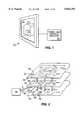
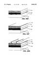
- FIG. 1is a perspective view of a display device.
- FIG. 2is a perspective schematic exploded view of a representative portion of the screen of FIG. 1.
- FIG. 3is an enlarged top view of a tri-dipole of FIG. 2.
- FIG. 4is a schematic view of a single dipole antenna of FIG. 3.
- FIG. 5is a schematic perspective view, broken away, of a portion of the screen of FIG. 1.
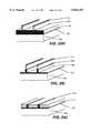
- FIG. 6is an enlarged top view of an individual tri-bus of FIG. 2.
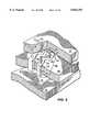
- FIG. 7is an enlarged perspective view of a representative portion of the screen of FIG. 1.
- FIG. 8is a cross-sectional view along 8--8 of FIG. 7.
- FIG. 9is a diagram of a portion of a control circuit of FIG. 2, and a corresponding dipole antenna of FIG. 3.
- FIGS. 10A, 10B, 10Care representative graphs of the input voltage to the bias source of FIG. 9.
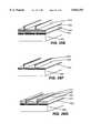
- FIG. 11is a diagram of portions of the control modules for a row of pixels
- FIG. 12is a circuit diagram of an oscillator.
- FIG. 13is a schematic diagram of a circuit module of FIG. 2, a corresponding dipole antenna of FIG. 3, and a graphical representation of the output of a binary counter.
- FIG. 14is a circuit diagram of the pulse counter of FIG. 13.
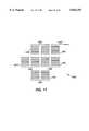
- FIGS. 15, 16, 17, 18, and 19are top views of alternative dipole arrangements.
- FIGS. 20A through 20Dare perspective views of a cavity device.
- FIGS. 21A and 21Bare side views of the cavity device.
- FIGS. 22A through 22Fare graphs of frequency responses of the cavity device in different states.
- FIGS. 23A and 23Bare top and cutaway side views, respectively, of a display.
- FIGS. 23C and 23Dare top and cutaway side views, respectively, of another display.
- FIG. 24Ais a graph of an electromechanical response of the cavity device.
- FIG. 24Bis a graph of an addressing and modulation scheme for a display.
- FIGS. 25A through 25N and FIGS. 26A through 26Kare perspective views of the device during assembly.
- FIGS. 27A through 27Care side views of dielectric mirrors.
- FIG. 27Dis a top view of a dielectric mirror.
- FIGS. 28A, 28Bare perspective and top views of a linear tunable filter.
- FIGS. 29A, 29Bare perspective and top views of a deformable mirror.
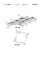
- device 20includes a screen 22 for displaying or sensing a high resolution color image (or a succession of color images) under control of power and control circuitry 26.
- the imageis made up of a densely packed rectangular array of tiny individual picture elements (pixels) each having a specific hue and brightness corresponding to the part of the image represented by the pixel.
- the pixel density of the imagedepends on the fabrication process used but could be on the order of 100,000 pixels per square centimeter.
- each pixelis generated by one so-called tri-dipole 30.
- the boundary of each tri-dipoleis T-shaped.
- the tri-dipolesare arranged in rows 32 in an interlocking fashion with the "Ts" of alternating tri-dipoles oriented in one direction and the "Ts" of intervening tri-dipoles along the same row oriented in the opposite direction.
- the rowstogether form a two-dimensional rectangular array of tri-dipoles (corresponding to the array of pixels) that are arranged on a first, external layer 34 of screen 22.
- the arraymay be called an electrically alterable optical planar array, or a visible spectrum modulator array.
- tri-busses 38are arranged in an interlocking two-dimensional array 40 corresponding to the layout of the tri-dipoles on layer 34 above.
- Each tri-dipole 30is connected to its corresponding tri-bus 38 by a multi-conductor link 42 running from layer 34 to layer 36 in a manner described below.
- a set of circuit modules 46are arranged in a two-dimensional rectangular array corresponding to the layouts of the tri-dipoles and tri-busses.
- Each circuit module 46is connected to its corresponding tri-bus 38 by a six-conductor link 48 running from layer 36 to layer 44 in a manner described below.
- Each circuit module 46electronically controls the optical characteristics of all of the antennas-of its corresponding tri-dipole 30 to generate the corresponding pixel of the image on screen 22.
- Circuit modules 46are connected, via conductors 50 running along layer 44, to an edge of layer 44.
- Wires 52connect the conductors 50 to control and power circuitry 26 which coordinates all of the circuit modules 46 to 25 generate the entire image.
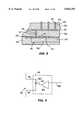
- each tri-dipole 30has three dipole sections 60, 62, 64.
- the center points 59, 61, 63 of the three sectionsare arranged at 120 degree intervals about a point 65 at the center of tri-dipole 30.
- Each section 60, 62, 64consists of a column of dipole antennas to 66, 68, 70, respectively, only ten dipole antennas are shown in each section in FIG. 3, but the number could be larger or smaller and would depend on, e.g., the density with which control circuits 46 can be fabricated, the tradeoff between bandwidth and gain implied by the spacing of the antennas, and the resistive losses of the conductors that connect the antennas to the control circuit 46.
- the dipole antennas of a given sectionall have the same dimensions corresponding to a particular resonant wavelength (color) assigned to that section.
- the resonant wavelengths for the three sections 60, 62, 64are respectively 0.45 microns (blue), 0.53 microns (green), and 0.6 microns (red).
- each dipole antenna 80schematically includes two Ls 82, 84 respectively made up of bases 86, 88, and arms 90, 92.
- the bases of each antenna 80are electrically connected to the corresponding circuit module 46.
- the span (X) of arms 90, 92is determined by the desired resonant wavelength of dipole antenna 80; for example, for a resonant wavelength of lambda, X would be lambda/2.
- Dipole antennas 66, 68, 70have X dimensions of 0.225 microns (lambda 1 ,/2), 0.265 microns (lambda 2 /2), and 0.3 microns (lambda 3 ,/2), respectively.
- the effective length (Y) of bases 86, 88 from arms 90, 92 to circuit module 46is also a function of the dipole antenna's resonant wavelength; for a resonant wavelength of lambda, Y is a multiple of lambda.
- each of the bases 86, 88physically is made up of four segments; (1) one of the conductors 96 of link 42, (2) a portion 112 of tri-bus 38, (3) a short connecting portion 124 of tri-bus 38, and (4) one of the conductors 94 of link 48, which together define a path (e.g., the path shown as dashed line 97) with an effective length of Y from the arm (e.g., 92) to the circuit module 46.
- a pathe.g., the path shown as dashed line 97
- Spacing Zmay be chosen based on the bandwidth/gain tradeoff, and for example may be one quarter of the resonant wavelength for the dipole antennas of a given section (i.e., lambda/4, or 0.1125 microns (lambda 1 /4), 0.1325 microns (lambda 2 /4) and 0.15 microns (lambda 3 /4) for antennas 66, 68, 70, respectively).
- each tri-bus 38is formed of aluminum on layer 36 and has three zigzag shaped bus pairs 100, 102, 104 for respectively connecting dipole antennas of the corresponding sections 60, 62, 64 of tri-dipole 30.
- Bus pairs 100, 102, 104are connected to individual dipole antennas 66, 68, 70 via conductors of link 42 (FIG. 2) that are joined to the bus pairs at points, e.g., 106.
- Each bus pair 100, 102, 104has two parallel buses 108, 110.
- Bus 108electrically connects together the arms of the dipole antenna 5 of the corresponding section and, independently, the related bus 110 electrically connects together the arms 92 of the dipole antennas of that same section.
- Points 106delineate a series of fragments 112, 114, 116 on each of the three bus pairs 100, 102, 104, respectively. Each fragment forms part of one or more of the bases 86, or 88 and therefore contributes to the effective Y dimension.
- the lengths (Q) of fragments 112, 114, 116are one-half of the resonant wavelengths (i.e. lambda/2) of the sections 60, 62, 64, or 0.225 microns (lambda 1 ,/2), 0.265 microns (lambda 2 ,/2), and 0.3 microns (lambda 3 ,/2), respectively.
- the conductors of link 48are attached to tri-bus 38 at points 118, 120, 122 at the ends of buses 108, 110. Between points 118, 120, 122 and the first points 106 on along buses 108, 110 are fragments 124, 126, 128, which also form portions of the bases 86, 88 and are included to adjust the effective Y dimensions of those bases to be integer multiples of lambda/2.
- the lengths of the three fragments 124, 126, 128are 0.1125 microns, 0.1525 microns, and 0.1875 microns, respectively.
- each dipole antenna 80is physically formed (of aluminum) on an insulating semiconductor (e.g. silicon dioxide of silicon nitride) substrate 130 (part of layer 34) by x-ray or electron beam lithography or other technique suitable for forming submicron-sized structures.
- an insulating semiconductore.g. silicon dioxide of silicon nitride
- Tri-busses 38are formed on the upper-side of a second insulating semiconductor substrate 132 (part of layer 36).
- Circuit modules 46(not seen in FIG. 7) are part of a third insulating semiconductor substrate 134 (part of layer 44) and are connected by conductors 50 to gold contact pads 136 (only one shown, not to scale) formed on the edge of substrate layer 134.
- circuit module 46is formed in and on substrate 134 by any one of several monolithic processes.
- a section 138 of the substrate 134which has been previously coated with an insulating semiconductor oxide layer 140, is repeatedly masked (whereby small windows are opened in the oxide layer, exposing the semiconductor beneath) and exposed to n and p dopants to form the desired circuit elements (not shown in detail in FIG. 8).
- the individual circuit elementsare connected to each other and to external contact pad 136 (FIG. 7) by aluminum conductors 142, 50, respectively.
- aluminum conductors 142, 50are connected to each other and to external contact pad 136 (FIG. 7) by aluminum conductors 142, 50, respectively.
- holes 144are opened in oxide layer 140 and a sheet of aluminum is deposited, filling holes 144.
- the unwanted aluminumis removed, leaving only conductors 142, 50.
- Semiconductor substrate layer 132is deposited directly on top of the remaining exposed oxide layer 140 and conductors 142, 50.
- Holes 146are channels for the electrical conductors 147 of links 48, which connect tri-bus 38 and circuit module 46.
- Tri-bus 38is etched from a sheet of aluminum deposited onto the surface of layer 132. The deposition process fills holes 146, thereby forming the conductors of links 48.
- Substrate layer 130is deposited onto the surface of substrate layer 132 and tri-bus 38.
- the arms of dipole antennas 80are formed by depositing a sheet of aluminum onto the surface of layer 130 and etching away the unwanted metal. During the deposition process holes 148 are filled thereby forming the conductors 149 of links 42 between the arms of dipole antenna 80 and tri-bus 38.
- the conductors 149are the uppermost parts of bases 86, 88 (FIG. 4) of dipole antennas 66, 68, 70; the lengths of conductors 149 together with the lengths of fragments 112, 114, 116 (FIG. 6), the lengths of fragments 124, 126, 128, and the lengths of the conductors 147 determine the effective Y dimension of bases 86, 88.
- the length of the conductors 149is determined by the thickness of the substrate 130 through which links 42 pass.
- Substrate 130 and links 42are 0.05625 microns (i.e. lambda 1 ,/8) thick. This thickness is achieved by controlling the deposition rate of the semiconductor material as layer 130 is formed.
- the length of the conductors 149is determined by the thickness of the substrate layer 132 through which they pass. This layer and links 48 are therefore also 0.05625 microns 20 thick.
- the Y dimensions for the dipole antennas 66, 68, 70 of sections 60, 62, 64therefore are as follows:
- Yequals the sum of 0,05625 microns (length of conductor in link 42,lambda 1 /8)+n * 0.3 microns (where 0.3 microns-lambda 3 /2, the length of a fragment 116, and n equals the number of fragments 116 in each base 86, 88 of the nth dipole antenna 70n)+0.1875 microns (the length of fragment 128, (lambda 3 /2)-(lambda 1 /4))+0.05625 microns (length of conductor in link 48), and that sum equals (n+1) * (lambda 3 /2).
- the displayed imageis not emitted from device 20 but is comprised of ambient light (or light from a source, not 25 shown) selectively reflected by the tri-dipoles 30 of screen 22.
- each tri-dipole 30receives ambient light having a broad spectrum of wavelengths and is controlled by the corresponding circuit module to reflect only that portion of the ambient light manifesting the hue and brightness of the desired corresponding pixel.
- the hue generated by tri-dipole 30depends on the relative intensities of the light reflected by sections 60, 62, 64.
- the overall brightness of that hue of lightin turn depends on the absolute intensities of the light radiation reflected by sections 60, 62, 64.
- both the hue and brightness of the light generated by tri-dipole 30can be controlled by regulating the intensity of the light reflected by the dipole antennas in each section of the tri-dipole; this is done by controlling the reflectivity of each dipole antenna, i.e.. the percentage of the light of the relevant wavelength for that dipole antenna which is reflected.
- the desired percentageis attained not by regulating the amount of light reflected at any given instant but by arranging for the antenna to be fully reflective in each of a series of spaced apart time slots, and otherwise non-reflective.
- Each dipole antennain conjunction with its circuit module, has only two possible states: either it reflects all of the light (at the antenna's resonant frequency), or it reflects none of that light.
- the intensityis regulated by controlling the percentage of total time occupied by the time slots in which the dipole antenna occupies the first state.
- Each dipole antennais controlled to be reflective or not by controlling the impedance of the dipole antenna relative to the impedance of the medium (e.g., air) through which the light travels. If the medium has an effective impedance of zero, then the relationship of the reflectivity of the dipole antenna to zero (the controlled impedance of the dipole antenna) can be derived as follows.
- the incident plus reflected wave for z ⁇ 0may be represented as: ##EQU1##
- E (overbar)is the complex amplitude of the electric field of the sum of the transmitted wave and the reflected wave
- E ois the complex amplitude of the electric field of the transmitted 20 wave
- E ris the complex amplitude of the electric field of the reflective wave
- x(hat)is the orientation of the electric field of the wave
- His the amplitude of the magnetic field
- y(hat)is the orientation of the magnetic field
- gois the permeability of free space
- ⁇ ois the permittivity of free space
- k⁇ sqrt ⁇ o ⁇ o !
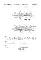
- the impedance z L , of dipole antenna 80is controlled by a variable resistance PIN diode 160 connected across bases 86, 88.
- PIN line 162to the output of a bias high voltage or a low voltage based on a line 168 from power and the output of bias source 164 is a high voltage
- the resistance R of PIN diode 160 (and hence the impedance (E,) of the dipole antennais zero causing full reflection
- resistance Ris set to a value such that the resulting impedance z@ is matched to z. (the impedance of the air surrounding the antenna), causing zero reflection.
- power and control circuitry 26receives a video signal (e.g. a digitized standard RGB television signal) and uses conventional techniques to deliver corresponding signals to modules 46 which indicate the relative desired intensities of light reflected from all sections 60, 62, 64 of all of the tri-dipoles in the array at a given time.
- Circuit modules 46use conventional techniques to deliver an appropriate stream of input control signal pulses to each bias source 164 on line 168.
- pulse stream 170has a period T and a 50% duty cycle.
- pulse stream 170has a period T and a 50% duty cycle.
- the input to bias source 164is high and the corresponding output of source 164 is a high voltage.
- dipole antenna 80will reflect all received light having the dipole antenna's resonant wavelength.
- the output of source 164will be low and dipole antennas 80 will absorb the received light.
- 10B, 10C, pulse streams 172, 174represent a 30% duty cycle and a 100% duty cycle respectively; with a 30% duty cycle the effective intensity of the light radiation of the dipole antennas of the section will be 30%; for a duty cycle of 100%, the effective intensity is 100%.
- the relative intensities required of the three red, 25 green, and blue sections 60, 62, 64may be, respectively, 30, 40, and 10.
- the input signals to the bias sources 164, carried on lines 168,would then have duty cycles, respectively, of 30%, 40%, and 10%.
- An adjacent pixel which is to be a brown of the same hue but greater brightnessmight require duty cycles of 45%, 60%, and 15%.
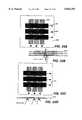
- each circuit module 46 in the rowincludes storage 180, 182 for two bits.
- the bit 1 storage elements 180 of the modules 46 in the roware connected together to create one long shift register with the pulse width modulated signals being passed along the row data line 184 from pixel to pixel. If, for example, the period of the modulated signals is 1 millisecond and there are ten different intensity levels, then an entire string of bits (representing the on or off state of the respective pixels in the row during the succeeding 1/10 millisecond) is shifted down the row every 1/10 millisecond.
- each element 182is the input to the driver 188 for the appropriate one of the three colors of that pixel, which in turn drives the corresponding section 60, 62, 64 of the tri-dipole.
- the rate at which data is shifted along the shift registersis determined by the number of elements on a given row, the number of rows, the number of intensity levels, and the refresh rate of the entire array.
- the light comprising the imageis emitted by tri-dipoles 30 rather than being produced by reflected ambient light.
- each tri-dipolegenerates the light for a single pixel with a hue and brightness governed by the intensities of the light emitted by each of the three sections 60, 62, 64.
- Each dipole antenna within a tri-dipoleis caused to emit light at the resonant wavelength of that antenna by stimulating it using a signal whose frequency corresponds to the resonant wavelength.
- the sections 60, 62, 64will emit blue (lambda 1 ), green (lambda 2 ), and red (lambda 3 ) light respectively when provided with signals whose frequencies equal, respectively, lambda 1 , lambda 2 and lambda 3 .
- ⁇is the charge density
- z(hat)indicates the direction of the current (along the z-axis); ⁇ angular frequency; and d is the distance between ideal point charges representing the dipole.
- the vector potential A(overbar) in polar coordinatesis given by ##EQU4## where ⁇ represents the angle relative to the dipole; ⁇ (hat) is the angular orientation of the wave; ⁇ o is the permeability of free space; r is radius from the dipole; r(hat) is radial orientation of the wave; A r is the radial component of the vector potential; A.sub. ⁇ is the angular component of the vector potential; and k is a factor which is used to represent sinusoidally varying waves.
- the H fieldis given by
- Equation (16)describes the radiation pattern away from a dipole antenna at distances significantly greater than the wavelength of the emitted electromagnetic wave. It is a very broad radiation pattern providing a wide field of view at relevant distances.
- the dipole antennas 66, 68, 70 of each section 60, 62, 64are driven by signals (e.g., sinusoidal) with frequencies of 5 ⁇ 10 14 Hz, 5.6 ⁇ 10 14 Hz, and 6.6 ⁇ 10 14 Hz for red, green, and blue, respectively.
- signalse.g., sinusoidal
- These signalsare supplied by three monolithic oscillators 200 (one shown) within circuit module 46, each tuned to one of the three required frequencies.
- circuit 200an a stable multivibrator
- the center pair of coupled transistors 202, 204are the primary active elements and will oscillate if the circuit admittance's are set appropriately.
- Diodes 206, 208, 210, 212provide coupling capacitance's between the transistors and the inductors 214, 216 are used to tune the operating frequency.
- an image of the objectis focused by a conventional lens (not shown in FIG. 1) onto screen 22, which then acts as an image sensor.
- the tri-dipoles of screen 22, controlled by power and control circuitry 26,generate electrical signals corresponding to pixels of the received image.
- the signalsare then processed by a processor which, in conventional fashion, delivers a derived RGB video signal which can then be transmitted or stored.
- the signals generated for each tri-dipoleare generated by the corresponding circuit module 46 and represent the hue and brightness of the light radiation received at that tri-dipole.
- circuit module 46can, by independently measuring the intensity of the light radiation received at each section 60, 62, 64, derive a signal which specifies the hue and intensity of the received pixel.
- dipole antenna 80will absorb incident light radiation at its resonant wavelength when its reflection coefficient ( ⁇ L ) is zero, which occurs when its controlled impedance (z L ) matches the impedance of the medium (z o ). In those circumstances, a voltage pulse is produced across the ends 308, 310 of dipole 80 for each incident photon. The relative magnitude of the light radiation received by each dipole antenna can thus be measured by counting the average number of pulses across ends 308, 310 over a given time period.
- circuit module 46includes a terminating load resistor 315 connected across ends 308, 310.
- the controlled impedance of the combination of dipole antenna 80 and resistor 315is equal to z o .
- the voltage of the pulse across resistor 315(created by an incident photon) is illustrated by the sine wave graph above register 15 and is described generally by the following equation
- a pulse detector 318amplifies and sharpens the resulting pulse to a square wave form as shown, which is then used as the clock (CLK) input 319 to a binary counter 320.
- the output of the binary counteris sampled at a regular rate; collectively the samples form a digital signal representing the intensity of received light radiation over time.
- Each time counter 320is sampled, it is reset to zero by a pulse on control line 322, Counter 320 thus serves as a digital integrator that indicates how much light arrived in each one of a succession of equal length time periods.
- the pair of transistors 322, 324serve as a high impedance differential stage whose output (representing the voltage difference between points 308, 310) is delivered to an amplifier 326.
- Amplifier 326serves as a high-bandwidth gain stage and delivers a single sided output pulse to a conditioning circuit 328 that converts slow rising pulses to square pulses 330 for driving counter 320.
- the array of tri-dipolesis operated as a phased array.
- phased arraysThe operation of phased arrays is discussed more fully in Amitay, et al., Theory and Analysis of Phased Array Antennas, 1972, incorporated herein by reference.
- wave cancellation or reinforcementcan be used to control the direction in three dimensions and orientation of the radiation. Beams can thus be generated or scanned.
- the arraycan be made more sensitive to radiation received from selected directions.
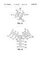
- each section of tri-dipole 400 arraybe a single dipole antenna 406, 407, 408.
- the tri-dipole antennasare then arranged about a center Point 410 at 120 degree intervals in a radial pattern.
- Bases 411, 412, as well as arms 414, 415, of the dipole antennas,are all formed on the same surface.
- each sectionmay consist of multiple dipole antennas 406, 407, 408 connected by attaching the bases 411, 412 of each succeeding dipole antenna to the inner ends of arms 414, 415 of the preceding dipole antenna.
- Circuit modules 416are formed on the surface of layer 413.
- a multi-dipole 430could have five sections 432, 434, 436, 438, 440 composed of dipole antennas 442, 444, 446, 448, 450, respectively.
- the dipole antennas of the different sectionswould have different resonant wavelengths.
- Other multi-dipolesmight have any number of sections.
- the scanning of pixelscould be done other than by pulse width modulation, for example, using charge coupled devices to shift packets of charge along the rows of pixels.
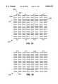
- each section 470 of a tri-dipole in the reflective modecould be formed of a number of subsections (e.g., 472) arranged in two rows 474 and a number of columns 47.
- the antennas 478 in each subsection 472are all served by a single PIN diode circuit 480 located at the peripheral edge of section 470 at the end of the subsection on the layer below the antenna layer. All circuits 480 for the entire Section 470 are in turn served by a single bias source 164 (FIG. 9). This arrangement reduces the number of bias sources required for the entire array of tri-dipoles.
- FIG. 19shows an alternate arrangement in which there is but one row of subsections each served by a single PIN diode circuit at the end of the row.
- selected tri-dipolescould be used to receive control signals transmitted directly by light and to pass those control signals to the control circuits of nearby active tri-dipoles.
- the dipolescould be mono-dipoles comprised of only a single dipole antenna, all with the same resonant wavelength.
- Dipole antennas 470could be randomly arranged on the surface of layer 472 of screen 22.
- RGBRed, Green, Blue
- the arraycould be three-dimensional.
- the successive tri-dipoles in the arraycan be oriented so that their respective antennas are orthogonal to each other to enable the array to interact with radiation of any arbitrary polarization.
- the PIN diodescould be replaced by other impedance controlling elements. Such elements might include quantum well transistors, superconducting junctions, or transistors based on vacuum microelectronics. Further improvement could be achieved by reducing the complexity of the third layer containing control circuitry. The electronics required to get control signals to the circuitry could be eliminated by the use of laser or electron beams to provide such signals. This would have the advantage of allowing for arrays of even higher density.
- the arraycould be fabricated on a transparent substrate, thus facilitating transmissive operation.
- the antenna arraysalone (without control circuitry or connection buses) may be fabricated on one-half of a microfabricated interferometric cavity.
- the antenna arraycan be considered a frequency selective mirror whose spectral characteristics are controlled by the dimensions of the antennas.
- Such a cavitywill transmit and reflect certain portions of incident electromagnetic radiation depending on (a) the dimensions of the cavity itself and (b) the frequency response of the mirrors.
- the behavior of interferometric cavities and dielectric mirrorsis discussed more fully in Macleod, H. A., Thin Film Optical Filters, 1969, incorporated by reference.
- two example adjacent elements of a larger array of this kindinclude two cavities 498, 499 fabricated on a transparent substrate 500.
- a layer 502the primary mirror/conductor, is comprised of a transparent conductive coating upon which a dielectric or metallic mirror has been fabricated.
- Insulating supports 504hold up a second transparent conducting membrane 506.
- Each array elementhas an antenna array 508 formed on the membrane 506.
- the two structures, 506 and 508,together comprise the secondary mirror/conductor.
- the antenna arraymay be fabricated as part of the primary mirror/conductor.
- Secondary mirror/conductor 506/508forms a flexible membrane, fabricated such that it is under tensile stress and thus parallel to the substrate, in the undriven state.
- the interferencewill determine its effective impedance, and thus its reflective and/or transmissive characteristics.
- the cavity heighti.e., the spacing between the inner walls of layers 502, 506
- the change in heightis achieved by applying a voltage across the two layers at the cavity, which, due to electrostatic forces, causes layer 506 to collapse.
- Cavity 498is shown collapsed (7 volts applied), while cavity 499 is shown uncollapsed (0 volts applied).
- each cavitymay be formed by a combination of dielectric or metallic mirrors on the two layers, and without the antennas formed on either layer.
- the spectral characteristics of the mirrorare determined by the nature and thickness(es) of the materials comprising it.
- each cavityis fabricated using a simpler process which precludes the need for separately defined support pillars.
- each secondary mirror/conductor, 506is formed in a U-shape with the legs attached to the primary layer; each secondary mirror/conductor thus is self-supporting.
- FIG. 20dthe cavity has been modified to alter it's mechanical behavior.
- a stiffening layer, 510has been added to limit deformation of the membrane while in the driven state. This assures that the two mirrors will remain parallel as a driving voltage is gradually increased.
- the resulting devicecan be driven in analog mode (e.g., cavity 511 may be driven by 5 volts to achieve partial deformation of the cavity) so that continuous variation of its spectral characteristics may be achieved.
- the binary modulation modeis shown in FIG. 21A.
- incident light 512the delta lambda represents a range of incident frequencies, e.g., the range of visible light
- the delta lambda nthe spectral component which is at the resonant frequency of the device in the undriven state. Consequently this component (delta lamba n) is transmitted, 516, and the remaining components (at nonresonant frequencies, delta lambda minus delta lamba n) are reflected, 514.
- This operationis in the nature of the operation of a fabry-perot interference cavity.
- the resonant frequency of the deviceWhen the device is driven and the geometry altered to collapse (right side of figure), the resonant frequency of the device also changes. With the correct cavity dimensions, all of the incident light (delta lamba) is reflected.
- FIG. 21Ashows a binary mode of operation while FIG. 21B shows an analog mode, where a continuously variable voltage may be used to cause a continuously variable degree of translation of secondary mirror/conductor 506.
- a continuously variable voltagemay be used to cause a continuously variable degree of translation of secondary mirror/conductor 506.
- Thisprovides a mechanism for continuous frequency selection within an operational range because the resonant frequency of the cavity can be varied continuously.
- the transmitted wavelengthsare delta lambda n zero, while in the right hand side they are delta lambda n one.
- Equation 1defines the transmission T through a fabry-perot cavity.
- Ta, Tb, Ra, Rbare the transmittances and reflectances of the primary (a) and secondary (b) mirrors.
- Phi a and Phi bare the phase changes upon reflectance at the primary and secondary mirrors, respectively.
- Deltais the phase thickness.
- Equation 2defines the phase thickness in terms of the cavity spacing ds, the index of refraction of the spacer ns, and the angle of incidence, theta s.
- Equation 3shows that the transmission T becomes the transmission of the second mirror when the transmission of the first mirror approaches 0.
- FIGS. 22A through 22Fillustrate some of the possibilities and relate to the equations of FIG. 21B. These are idealized plots which illustrate transmission and reflectivity (T/R) of the cavity for wavelengths in the visible range in driven and undriven states for each of the driven and undriven response modes. The different modes are achieved by using different combinations of mirrors and cavity spacings.
- the spectral characteristics of the mirrors usedcan be referred to as broad-band and narrow-band.
- the mirrorsare optimized for the visible range with a broad band mirror operating across the entire visible range (i.e., reflecting over a minimum range of 400 nm to 700 nm).
- a broad band mirroroperating across the entire visible range (i.e., reflecting over a minimum range of 400 nm to 700 nm).
- Such a mirroris denoted in the stack formula 1.671.linevert split.0.775(ERS) 0.833M (ERS).linevert split.1.671 where ERS denotes an equal ripple filter.
- a narrow-band filter optimized for the color greenwould reflect only over the range of 500 nm to 570 nm, and transmit everywhere else.
- the cavity spacing(i.e., cavity height) in both driven and undriven states can be set to a predetermined value by the film thicknesses used in its construction. These two values determine whether a cavity is resonant or non-resonant. For a resonant cavity, the spacing is determined such that the undriven state coincides with the resonant peak of the narrower of the two mirrors. When a device is non-resonant, it must be driven in order for the device to become resonant.
- FIG. 22Ashows a T/R plot of a cavity having broad band mirrors on both layers of the cavity.
- thisresults in transmission/reflection peaks which occur at wavelengths which are approximately integral multiples of the cavity spacing.
- the notation m delta lambda n in FIG. 21Adenotes the fact that there may be a series of peaks.
- Thisis classic fabry-perot behavior.
- the driven stateshown to the right in FIG. 22A
- the cavity resonanceis shifted out of the visible range causing the device to act like a broadband mirror.
- FIG. 22Bshows a T/R plot for a cavity having one broad band and one narrow band mirror.
- This devicehas a resonant cavity, causing a transmission peak at the center of the narrow-band mirror's passband when the device is in the undriven state.
- Driving the device(right hand side of FIG. 22B) shifts the cavity resonance away from that of the narrow band mirror, and the device acts like a broadband mirror.
- the cavityis like that of FIG. 22B, except the cavity is non-resonant which results in broadband mirror cavity behavior in the undriven state.
- the cavity spacingshifts into resonance, causing a transmission peak centered on the narrow-band mirror.
- FIG. 22Dshows the performance of a resonant cavity with two narrow-band mirrors.
- the overall cavity responseis that of a broad-band transmitter.
- Driving the device out of resonancei.e. active
- the cavity of FIG. 22Ehas two narrow band mirrors, but it is a non-resonant cavity. Consequently its behavior is opposite that of the cavity portrayed in FIG. 22D.
- the transmissionapproaches zero for frequencies outside its range. This is essentially the transmission of mirror b.
- the transmissionbecomes a maximum outside the frequency range. In either case, the spurious peaks typical of a fabry-perot are avoided. The result is a device which can be described as a single mode resonant cavity.
- both of the mirrorsare narrow banded, then fabry-perot type behavior occurs only when the cavity spacing is correct. Making the mirrors narrow enough allows only a single peak to occur. Then it is unnecessary to be concerned about spurious peaks that might occur within the visible range.
- FIG. 22Fis for a cavity with a simpler design involving only a metallic mirror on one wall and a hybrid filter on the other wall.
- the hybrid filteris a combination of a narrow bandpass filter (outer surface) and an induced absorber (inner surface).
- the induced absorberis a simple structure which can consist of one or more dielectric or dielectric and metallic films. The function of the absorber is to cause incident light of a specified frequency range to be absorbed by a reflective surface (i.e. mirror).
- the induced absorberonly functions when it is in contact with the mirror, otherwise it is inconsequential.
- the hybrid filter(a green centered narrow bandpass/induced absorber) reflects everything but the green light, which is unaffected by the induced absorber and subsequently reflected by the metallic mirror.
- the overall cavity responseis like that of a broad-band mirror.
- the hybrid filtercomes into contact with the metallic mirror.
- the absorbercouples the green light into the mirror, and the result is an absorption peak at that wavelength.
- a red 3 ⁇ 3 pixel (i.e., 9 cavities) subtractive mode display array based on the cavity device using the N--N (narrow band-narrow band) configuration of FIG. 22Dis shown.
- the cavity pixelsare formed at the intersections of primary mirror/conductors 602 and secondary mirror/conductors 604.
- the displayis fabricated on substrate 608 and driven via contact pads 606 connected to each conductor/mirror 604.
- a full nine-pixel displaycomprises three replications of the array of FIG. 23A arranged on top of one another and fabricated on separate substrates or color planes 610, 612, 614, as shown in FIG. 23B.
- Each of the individual color planesinteracts only with and reflects one color (e.g., red, green, or blue), while passing all other colors. This is done by selecting the mirror spectral characteristic and cavity spacing in each color plane appropriately.
- the color planesare physically aligned and electrically driven through the contact pads to produce full color images. The image would be viewed from below in FIG. 23B.
- Pixel size and overall display sizecan be altered to make the displays useful in many different display and spatial light modulator applications. These include direct view and projection displays, optical computing, holographic memory, and any other situation where a one or two dimensional modulator of light can be used.
- the secondary mirror/conductorexperiences a displacement towards the substrate until the force of restoration balances the electrical attraction.
- the force of restorationis completely overcome and the membrane is pressed tightly against the substrate.
- the voltagecan then be lowered again to some degree without affecting the position of the membrane. Only if the voltage is then lowered significantly or eliminated will the membrane be released. Because the membrane is under tensile stress, it will then pull itself away from the substrate when the voltage is released. This hysteresis can be used to achieve matrix addressing of a two-dimensional array, as explained with reference to FIG. 24B.
- the displaycan be addressed and brightness controlled using control pulse sequences in the driving voltage. Shown is a timing diagram for a 3 ⁇ 3 pixel array analogous to that shown in FIG. 23A.
- a continuous series of -5 volts scanning pulsesis applied to the rows (rows 1-3) of the pixel array in a sequential fashion, as seen in the charts labelled "Row".
- the pulsesappear at the same frequency on each of the rows but the pulses for different rows are staggered. These pulses are insufficient in their own right to cause the membrane to collapse.
- the columns (cols. 1-3) of the pixel array(see charts labelled "Col) are maintained at a bias voltage of 5 volts so that the nominal voltage across each unactivated pixel is 5 volts.
- the nominal row and column potentialsare 5 and -5 volts respectively, resulting in a cavity voltage of 10 volts.
- the total voltage across the cavitybecomes 15 volts which is sufficient to drive the secondary mirror/conductor into the collapsed state, where it will remain until the end of the scan when all of the column voltages are pulsed to zero.
- the three charts at the bottom of FIG. 24Bshow the on and off states of the three pixels identified there by row and column numbers.
- the intensity or brightness of a pixelmay be varied by changing the fraction of the scan during which the pixel is activated.
- the scan cyclebegins at 198 and ends at 199.
- the frequency of the scan pulsesis such that six pulses of a given row fall within the scan cycle, providing an opportunity to activate a pixel at any one of six times during each cycle. Once the pixel is activated it stays on until the end of the cycle. Therefore six different intensities are possible for each pixel.
- pixel C1R1is at full brightness
- pixel C2R2is at 4/6 brightness
- pixel C3R2is at 1/6 brightness. All pixels are cleared at the end of the scan and the cycle begins again. Since these structures can be driven at frequencies as high as 50 kHz, this method of brightness control is practical. Assuming six brightness levels, there would be a possibility of more than 8 thousand row scans per second.
- substrate 700is first cleaned using standard procedures.
- the substratemay be of many different materials including silicon, plastic, mylar, or quartz.
- the primary requirementis that the material be able to support an optically smooth, though not necessarily flat, finish.
- a preferred materialwould likely be glass, which would permit both transmissive and reflective operation in the visible range.
- the substrateis then coated with the primary conductor/mirror layer(s) 702.
- Thiscan be achieved using a physical vapor deposition (PVD) method such as sputtering or e-beam evaporation.
- PVDphysical vapor deposition
- Other possible methodsinclude chemical vapor deposition and molecular beam epitaxy.
- the dimensions and nature of the layer(s)depend on the specific configuration desired. Detailed examples are discussed below.
- a photoresist 704has been patterned on the primary conductor/mirror.
- the photoresistmay be of a positive or negative type.
- the standard procedure for this stepinvolves spinning of the resist, softbaking at 90 C, exposing through an appropriate mask, developing to produce the pattern, and hardbaking at 130 C.
- the photoresist patternis defined in the primary conductor/mirror by an etching process.
- This stepcan be achieved either by wet chemical means or by plasma or reactive ion etching (RIE).
- RIEreactive ion etching
- the choice of etching techniquedepends on the nature of the conductor/mirror. In the case of an aluminum conductor/mirror, chlorine gas may be used to perform the etch, with a standard chamber power of 100 watts producing an etch rate of 100 angstroms/min. Some mirror materials may resist RIE and in such cases a technique such as ion milling may be used. All RIE steps are performed at a pressure of 30 mtorr unless otherwise noted. All plasma etch steps are performed at a pressure of 100 mtorr unless otherwise noted. The photoresist is removed using standard solvents.
- the conductor/mirrormay be defined using the well-known procedure called lift-off. This procedure is used to define a layer in a subsequent step and is described below.
- support rail material 706,has been deposited using one of the methods mentioned previously.
- This materialshould be an insulator, for example silicon dioxide or silicon nitride.
- the materialshould be deposited uniformly, and at a thickness equal to thickness of the spacer layer, which will be deposited later. This thickness should in general be at least a multiple of the wavelength of light of interest. A thickness of 0.5 microns would place such a device near the middle of the visible spectrum.
- photoresist layer 708is spun on and hardbaked. Since this layer will not be photolithographically defined, other polymeric materials may be used instead. The only requirement is that they dissolve in solvents such as acetone or methanol, and be able to withstand a vacuum. This is the first step in defining a lift-off stencil.
- template layer 710has been deposited using one of the methods of PVD.
- the layeris of silicon dioxide though other materials are possible. Ideally the material should be etched using a process which does not affect the underlying resist.
- Buffered Oxide Etch (BOE)which consists of Hydrofluoric acid diluted 7:1 with water can perform this step in 15 seconds.
- the layerneed only be a thousand angstroms thick.
- photoresist layer 712has been spun-on and patterned in a manner already discussed.
- the pattern of resist layer 711has been transferred to layers 710 and 708.
- the BOEis used to etch through the silicon dioxide layer 710.
- An oxygen plasmais used to etch through resist layer 708, and to remove resist layer 711.
- Plasma etchingdiffers from RIE in that it tends to be less anisotropic, yielding profiles that are not purely vertical.
- resist layer 708has been slightly underetched in order to facilitate removal of the lift-off stencil.
- RIEusing a carbon tetrafluoride chemistry (CF4/02 6:4) is then applied to etching through layer 706.
- spacer layer 712is deposited using PVD techniques.
- This materialcan be any number of different compounds which can be deposited using this technique. There are two key requirements for such a material. The first is that the material be soluble in water but not in solvents such as acetone or methanol. Example materials include lithium fluoride, aluminum fluoride, and sodium chloride. The second is that it be deposited with extreme uniformity and thickness control.
- the formerallows resulting structures to be underetched without damage by using water as the final etchant.
- Wateris an extremely benign solvent, and makes possible the incorporation of many different mirror, conductor, and structural materials in the final device.
- the spacermay also be composed of a polymeric material such as hardbaked photoresist or polyimide.
- a technique other than spinningmust be used to deposit the polymer. Two such techniques include extrusion and capillary coating. The consequence of using such a spacer is that all subsequent process steps must be low temperature in nature to prevent outgassing and shrinkage of this layer. In this case, the spacer is ultimately removed using an oxygen plasma.
- the stencilis subsequently removed using an ultrasonic acetone bath and methanol rinse. This also removes or lifts off excess deposited spacer material and is what constitutes the final step of the lift-off process.
- a natural overhangmay be produced via overexposure.
- positive photoresistusing a technique known as image-reversal. This would preclude the need to put down a sacrificial photoresist layer and a subsequent SiO2 layer.
- secondary conductor/mirror layer(s) and support membrane (714)are deposited.
- the nature of the conductor/mirroris dependent on the application.
- the support membranemust have a tensile residual stress. Tensile stress is required for two reasons. First so that the resulting membranes will be flat and therefore parallel to the substrate in the quiescent state. Secondly, such structures have a tendency to stick when the membranes come in contact with the substrate. Sufficient tensile stress is required pull the membrane away when the drive voltage is reduced.
- the membranemust have the appropriate optical characteristics as well. For visible light this would mean transparency in the visible region.
- Silicon nitrideis one candidate for this role for it can be deposited using plasma enhanced chemical vapor deposition (PECVD) with controlled stress.
- PECVDplasma enhanced chemical vapor deposition
- Other candidatesinclude silicon dioxide, magnesium fluoride and calcium fluoride, all of which can be deposited using e-beam evaporation with a resulting tensile stress.
- photoresist layer 716has been spun-on and patterned in a manner discussed above.
- layer(s) 714have been etched according to the pattern of resist layer 716.
- the final etchis accomplished by placing the device in water for a period of time.
- the wateris agitated, and when the devices are fully etched they are dried.
- One variation on this stepinvolves the use of n-butyl alcohol to displace the water when the etch is finished.
- the devicesare then placed in a chamber at approximately 32 degrees centigrade to cause the alcohol to freeze. After this step the devices are placed into a vacuum chamber where the air is then evacuated. This causes the alcohol to sublime and can reduce membrane sticking during the drying phase.
- FIGS. 26A through 26CAnother alternative process has initial steps of assembly shown in FIGS. 26A through 26C, analogous to those shown in FIGS. 25A through 25C.
- photoresist or polymer layer 806is spun on and a stencil layer, 208, of silicon dioxide is deposited using PVD. This layer must be thicker than the spacer layer to be deposited.
- resist layer 810has been spun-on and patterned using standard procedures.
- this stepuses BOE and an oxygen plasma etch to define a lift-off stencil.
- the spacer materialis chosen and deposited as described in FIG. 25J.
- the stencilis subsequently removed using an ultrasonic acetone bath and methanol rinse.
- the step shown in FIG. 26Iis analogous to that shown in FIG. 25K.
- photoresist layer 814has been spun-on and patterned.
- layer(s) 812have been etched according to the pattern of resist layer 214.
- the final etchis accomplished in a manner described above.
- All of the materials used for the mirrorsmust be deposited in such a way that their stress can be controlled. Ideally, they are deposited as "stress balanced" which means that the overall stress of the film or film stack is zero. Since the ultimate goal is that the support membrane conductor/mirror combination have an overall tensile stress, conductor/mirror films with compressive stress may be accommodated by having a high stress support membrane.
- the technique of ion assisted e-beam deposition (IABD)precludes the need for such accommodation. Using this technique, the residual stress of almost any film of interest may be controlled by bombarding the substrate with a stream of neutral ions during the deposition process. This make possible the total mechanical decoupling of the support material from the optical material. As a result, emphasis can be placed on depositing an optically neutral support membrane with ideal mechanical characteristics. In the same manner, a "mechanically neutral” (i.e. stressless) conductor/mirror can be deposited with ideal optical characteristic.
- the simplest conductor/mirror configuration for an individual cavityis formed from a layer 900 that is either the substrate for the primary conductor/mirror, or the support membrane if this is the secondary.
- Layer 902is a metallic film with a thickness on the order of several hundred angstroms. The film can be of aluminum, silver, or any number of metals, based on the spectral, and resistive properties as well as the ease with which the metal can be etched.
- Layer 904is an insulator and/or reflection enhancement film. This can be formed by oxidizing the metal, if aluminum is being used, in an oxygen plasma thus forming a thin layer of aluminum oxide. Alternatively, insulating layers or reflection enhancement layers may be deposited in a manner discussed before.
- Metallic mirrorsmust be somewhat transmissive and therefore no more than several hundred angstroms thick. Insulator films can have thicknesses from one hundred to several thousand angstroms. Their thickness is determined by the kind of voltages expected in driving the devices.
- the conductor 906is either a transparent film such as indium tin oxide (ITO), or a very thin metallic layer such as gold. Either can be deposited using suitable film deposition methods. Thicknesses for the ITO should be in the range of several thousand angstroms, and metallic conductors less than 100 angstroms.
- 908is a multilayer dielectric stack comprising the mirror. Such a mirror consists of alternating dielectric films with differing indexes of refraction deposited by a suitable PVD process. By choosing films with appropriate thicknesses and indexes, mirrors with tailorable spectral characteristics can be fabricated as is well known in the art. In general, the thickness of the individual layers is one quarter the wavelength of the light of interest.
- these mirrorsmay be deposited using a technique known as codeposition.
- codepositionIn this case, PVD is used to deposit two materials with different refractive indices simultaneously. Using computer control the refractive index of the resulting film can be varied continuously between those of either film. This deposition technique makes possible mirrors with virtually any spectral characteristic.
- a dielectric mirror 908is deposited directly on substrate 900.
- Metallic conductor 902 and insulator 904are deposited and patterned such that they form a border around the periphery of the mirror. Using this configuration, it is possible to provide drive voltages to the devices without compromising throughput since the conductor can be placed outside the active area of the device.
- FIG. 27Dshows a planar view of this mirror configuration.
- a linear tunable filteris shown which has been fabricated using the process sequence defined above.
- the major differenceis the nature of the mask used to define the self-supporting membrane, which is comprised of support 1006 and 1008.
- the substrate, 1000is transparent in the frequency region of interest, and electrodes 1004 are used to drive the device.
- Dielectric mirror 1002are defined separately to produce a configuration like that of FIGS. 27c, 27d.
- Three filtersare shown though many more can be fabricated. Each filter 1010, 1012, and 1014 is driven independently so that individual frequencies may be separated from an incident light beam.
- FIG. 28bis a top view of the structure.
- a device known as a deformable mirrorincludes a self-supporting membrane 1102 fabricated on a substrate 1100.
- a potentialis applied between actuator electrodes 1104 and conducting mirror 1106, the surface of the mirror can be deformed in a controllable manner.
- Such a devicecan be used as a component in an adaptive optics system, or in any situation where control of an incident wavefront is required.
Landscapes
- Physics & Mathematics (AREA)
- Engineering & Computer Science (AREA)
- General Physics & Mathematics (AREA)
- Optics & Photonics (AREA)
- Spectroscopy & Molecular Physics (AREA)
- Theoretical Computer Science (AREA)
- Computer Hardware Design (AREA)
- Chemical & Material Sciences (AREA)
- Nanotechnology (AREA)
- Life Sciences & Earth Sciences (AREA)
- Biophysics (AREA)
- Crystallography & Structural Chemistry (AREA)
- Mechanical Light Control Or Optical Switches (AREA)
- Devices For Indicating Variable Information By Combining Individual Elements (AREA)
- Micromachines (AREA)
Abstract
Description
x E.sub.o +E.sub.r !=xE.sub.t (5)
y(1/η.sub.o)(E.sub.o -E.sub.R)=y(1/η.sub.t)E.sub.t (6)
1+E.sub.r /E.sub.o =E.sub.t /E.sub.o (7)
1-E.sub.R /E.sub.o =(η.sub.o /η.sub.t)(E.sub.t /E.sub.o) (8)
I=jωσ (11)
J(r')=zIdδ(r') (12)
V(z)=V+e.sup.-jkz +Γ.sub.L e.sup.jkz (17)
V(z)=V+e.sup.-jkz (18)
Claims (46)
Priority Applications (51)
| Application Number | Priority Date | Filing Date | Title |
|---|---|---|---|
| US08/238,750US5835255A (en) | 1986-04-23 | 1994-05-05 | Visible spectrum modulator arrays |
| PCT/US1995/005358WO1995030924A1 (en) | 1994-05-05 | 1995-05-01 | Visible spectrum modulator arrays |
| JP52903095AJP3942040B2 (en) | 1994-05-05 | 1995-05-01 | Visible spectrum modulator array |
| EP95918880AEP0801766A4 (en) | 1994-05-05 | 1995-05-01 | Visible spectrum modulator arrays |
| US08/688,710US6040937A (en) | 1994-05-05 | 1996-07-31 | Interferometric modulation |
| US08/744,253US5986796A (en) | 1993-03-17 | 1996-11-05 | Visible spectrum modulator arrays |
| US09/056,975US6674562B1 (en) | 1994-05-05 | 1998-04-08 | Interferometric modulation of radiation |
| US09/238,340US6055090A (en) | 1994-05-05 | 1999-01-27 | Interferometric modulation |
| US09/413,222US7123216B1 (en) | 1994-05-05 | 1999-10-05 | Photonic MEMS and structures |
| US09/966,843US6867896B2 (en) | 1994-05-05 | 2001-09-28 | Interferometric modulation of radiation |
| US09/974,544US6680792B2 (en) | 1994-05-05 | 2001-10-10 | Interferometric modulation of radiation |
| US10/012,092US6650455B2 (en) | 1994-05-05 | 2001-11-13 | Photonic mems and structures |
| US09/991,378US20020075555A1 (en) | 1994-05-05 | 2001-11-21 | Interferometric modulation of radiation |
| US10/076,224US6710908B2 (en) | 1994-05-05 | 2002-02-13 | Controlling micro-electro-mechanical cavities |
| US10/078,282US7042643B2 (en) | 1994-05-05 | 2002-02-19 | Interferometric modulation of radiation |
| US10/644,312US7460291B2 (en) | 1994-05-05 | 2003-08-19 | Separable modulator |
| US10/752,140US7692844B2 (en) | 1994-05-05 | 2004-01-05 | Interferometric modulation of radiation |
| US10/844,802US7280265B2 (en) | 1994-05-05 | 2004-05-12 | Interferometric modulation of radiation |
| US11/056,571US7379227B2 (en) | 1994-05-05 | 2005-02-11 | Method and device for modulating light |
| US11/070,497US7012732B2 (en) | 1994-05-05 | 2005-03-01 | Method and device for modulating light with a time-varying signal |
| US11/192,436US7463421B2 (en) | 1994-05-05 | 2005-07-28 | Method and device for modulating light |
| JP2005292775AJP2006106756A (en) | 1994-05-05 | 2005-10-05 | Visible spectrum modulator array |
| US11/267,819US7776631B2 (en) | 1994-05-05 | 2005-11-04 | MEMS device and method of forming a MEMS device |
| US11/267,939US8014059B2 (en) | 1994-05-05 | 2005-11-04 | System and method for charge control in a MEMS device |
| US11/432,724US7848001B2 (en) | 1994-05-05 | 2006-05-11 | Method and system for interferometric modulation in projection or peripheral devices |
| JP2006140486AJP4027395B2 (en) | 1994-05-05 | 2006-05-19 | Visible spectrum modulator array |
| US11/438,913US7372619B2 (en) | 1994-05-05 | 2006-05-23 | Display device having a movable structure for modulating light and method thereof |
| US11/584,425US7619810B2 (en) | 1994-05-05 | 2006-10-20 | Systems and methods of testing micro-electromechanical devices |
| US11/626,792US8284474B2 (en) | 1994-05-05 | 2007-01-24 | Method and system for interferometric modulation in projection or peripheral devices |
| US11/668,973US7846344B2 (en) | 1994-05-05 | 2007-01-30 | Method and device for modulating light |
| US11/742,271US8059326B2 (en) | 1994-05-05 | 2007-04-30 | Display devices comprising of interferometric modulator and sensor |
| US11/754,229US7532381B2 (en) | 1994-05-05 | 2007-05-25 | Method of making a light modulating display device and associated transistor circuitry and structures thereof |
| JP2007189815AJP4639346B2 (en) | 1994-05-05 | 2007-07-20 | Display device including a plurality of reflection elements and manufacturing method |
| US11/841,795US8081369B2 (en) | 1994-05-05 | 2007-08-20 | System and method for a MEMS device |
| US11/841,833US7800809B2 (en) | 1994-05-05 | 2007-08-20 | System and method for a MEMS device |
| US11/841,741US7830587B2 (en) | 1993-03-17 | 2007-08-20 | Method and device for modulating light with semiconductor substrate |
| US11/841,810US7738157B2 (en) | 1994-05-05 | 2007-08-20 | System and method for a MEMS device |
| US11/841,752US7826120B2 (en) | 1994-05-05 | 2007-08-20 | Method and device for multi-color interferometric modulation |
| US11/841,726US7839556B2 (en) | 1994-05-05 | 2007-08-20 | Method and device for modulating light |
| US11/841,847US7848004B2 (en) | 1994-05-05 | 2007-08-20 | System and method for a MEMS device |
| US11/841,780US7808694B2 (en) | 1994-05-05 | 2007-08-20 | Method and device for modulating light |
| US11/841,820US7852545B2 (en) | 1994-05-05 | 2007-08-20 | Method and device for modulating light |
| US11/868,414US7605969B2 (en) | 1994-05-05 | 2007-10-05 | Interferometric modulation of radiation |
| US12/031,603US8105496B2 (en) | 1994-05-05 | 2008-02-14 | Method of fabricating MEMS devices (such as IMod) comprising using a gas phase etchant to remove a layer |
| US12/099,057US20080191978A1 (en) | 1994-05-05 | 2008-04-07 | Apparatus for driving micromechanical devices |
| US12/781,645US20100220248A1 (en) | 1994-05-05 | 2010-05-17 | Projection display |
| US12/815,136US8054532B2 (en) | 1994-05-05 | 2010-06-14 | Method and device for providing illumination to interferometric modulators |
| US12/902,524US20110026096A1 (en) | 1994-05-05 | 2010-10-12 | Method and device for multi-color interferometric modulation |
| US12/908,846US8035884B2 (en) | 1994-05-05 | 2010-10-20 | Method and device for modulating light with semiconductor substrate |
| US12/939,087US20110043891A1 (en) | 1994-05-05 | 2010-11-03 | Method for modulating light |
| US13/225,357US20120062310A1 (en) | 1994-05-05 | 2011-09-02 | System and method for charge control in a mems device |
Applications Claiming Priority (7)
| Application Number | Priority Date | Filing Date | Title |
|---|---|---|---|
| US85511686A | 1986-04-23 | 1986-04-23 | |
| US16677488A | 1988-03-04 | 1988-03-04 | |
| US29689689A | 1989-01-12 | 1989-01-12 | |
| US48979490A | 1990-03-05 | 1990-03-05 | |
| US79481991A | 1991-11-18 | 1991-11-18 | |
| US3271193A | 1993-03-17 | 1993-03-17 | |
| US08/238,750US5835255A (en) | 1986-04-23 | 1994-05-05 | Visible spectrum modulator arrays |
Related Parent Applications (3)
| Application Number | Title | Priority Date | Filing Date |
|---|---|---|---|
| US3271193AContinuation-In-Part | 1986-04-23 | 1993-03-17 | |
| US08/544,630Continuation-In-PartUS5651569A (en) | 1995-10-18 | 1995-10-18 | Inflatable bumper system |
| US55463095AContinuation-In-Part | 1993-03-17 | 1995-11-06 |
Related Child Applications (6)
| Application Number | Title | Priority Date | Filing Date |
|---|---|---|---|
| PCT/US1995/005358Continuation-In-PartWO1995030924A1 (en) | 1993-03-17 | 1995-05-01 | Visible spectrum modulator arrays |
| US55463095AContinuation-In-Part | 1993-03-17 | 1995-11-06 | |
| US76994796AContinuation-In-Part | 1994-05-05 | 1996-12-19 | |
| US09/056,975Continuation-In-PartUS6674562B1 (en) | 1993-03-17 | 1998-04-08 | Interferometric modulation of radiation |
| US09/413,222Continuation-In-PartUS7123216B1 (en) | 1994-05-05 | 1999-10-05 | Photonic MEMS and structures |
| US11/841,741Continuation-In-PartUS7830587B2 (en) | 1993-03-17 | 2007-08-20 | Method and device for modulating light with semiconductor substrate |
Publications (1)
| Publication Number | Publication Date |
|---|---|
| US5835255Atrue US5835255A (en) | 1998-11-10 |
Family
ID=22899150
Family Applications (2)
| Application Number | Title | Priority Date | Filing Date |
|---|---|---|---|
| US08/238,750Expired - LifetimeUS5835255A (en) | 1986-04-23 | 1994-05-05 | Visible spectrum modulator arrays |
| US08/744,253Expired - LifetimeUS5986796A (en) | 1993-03-17 | 1996-11-05 | Visible spectrum modulator arrays |
Family Applications After (1)
| Application Number | Title | Priority Date | Filing Date |
|---|---|---|---|
| US08/744,253Expired - LifetimeUS5986796A (en) | 1993-03-17 | 1996-11-05 | Visible spectrum modulator arrays |
Country Status (4)
| Country | Link |
|---|---|
| US (2) | US5835255A (en) |
| EP (1) | EP0801766A4 (en) |
| JP (4) | JP3942040B2 (en) |
| WO (1) | WO1995030924A1 (en) |
Cited By (441)
| Publication number | Priority date | Publication date | Assignee | Title |
|---|---|---|---|---|
| US5986796A (en)* | 1993-03-17 | 1999-11-16 | Etalon Inc. | Visible spectrum modulator arrays |
| US6040937A (en)* | 1994-05-05 | 2000-03-21 | Etalon, Inc. | Interferometric modulation |
| JP2002040238A (en)* | 2000-07-19 | 2002-02-06 | Sony Corp | Optical multilayered structural body, optical switching device and image display device |
| US6392775B1 (en)* | 1998-01-13 | 2002-05-21 | Seagate Technology Llc | Optical reflector for micro-machined mirrors |
| US20020070931A1 (en)* | 2000-07-03 | 2002-06-13 | Hiroichi Ishikawa | Optical multilayer structure, optical switching device, and image display |
| US6407851B1 (en) | 2000-08-01 | 2002-06-18 | Mohammed N. Islam | Micromechanical optical switch |
| US6445502B1 (en) | 2001-02-02 | 2002-09-03 | Celeste Optics, Inc. | Variable blazed grating |
| US6449410B1 (en)* | 2001-03-16 | 2002-09-10 | Optic Net, Inc. | Two-dimensional tunable filter array for a matrix of integrated fiber optic input-output light channels |
| US6466354B1 (en) | 2000-09-19 | 2002-10-15 | Silicon Light Machines | Method and apparatus for interferometric modulation of light |
| US6493488B1 (en) | 2000-12-22 | 2002-12-10 | Celeste Optics, Inc. | Apparatus and method for high speed optical signal processing |
| US20030043157A1 (en)* | 1999-10-05 | 2003-03-06 | Iridigm Display Corporation | Photonic MEMS and structures |
| US6574033B1 (en) | 2002-02-27 | 2003-06-03 | Iridigm Display Corporation | Microelectromechanical systems device and method for fabricating same |
| US6587263B1 (en) | 2000-03-31 | 2003-07-01 | Lockheed Martin Corporation | Optical solar reflectors |
| US6589625B1 (en) | 2001-08-01 | 2003-07-08 | Iridigm Display Corporation | Hermetic seal and method to create the same |
| WO2003069413A1 (en) | 2002-02-12 | 2003-08-21 | Iridigm Display Corporation | A method for fabricating a structure for a microelectromechanical systems (mems) device |
| US6650455B2 (en) | 1994-05-05 | 2003-11-18 | Iridigm Display Corporation | Photonic mems and structures |
| US6674562B1 (en) | 1994-05-05 | 2004-01-06 | Iridigm Display Corporation | Interferometric modulation of radiation |
| WO2004006003A1 (en) | 2002-07-02 | 2004-01-15 | Iridigm Display Corporation | A device having a light-absorbing mask a method for fabricating same |
| US6680792B2 (en)* | 1994-05-05 | 2004-01-20 | Iridigm Display Corporation | Interferometric modulation of radiation |
| US6707591B2 (en) | 2001-04-10 | 2004-03-16 | Silicon Light Machines | Angled illumination for a single order light modulator based projection system |
| US6710908B2 (en) | 1994-05-05 | 2004-03-23 | Iridigm Display Corporation | Controlling micro-electro-mechanical cavities |
| US6712480B1 (en) | 2002-09-27 | 2004-03-30 | Silicon Light Machines | Controlled curvature of stressed micro-structures |
| US6714337B1 (en) | 2002-06-28 | 2004-03-30 | Silicon Light Machines | Method and device for modulating a light beam and having an improved gamma response |
| US6721473B1 (en) | 2001-02-02 | 2004-04-13 | Cheetah Omni, Llc | Variable blazed grating based signal processing |
| US6721475B1 (en) | 2000-12-22 | 2004-04-13 | Cheetah Omni, Llc | Apparatus and method for providing gain equalization |
| US6728023B1 (en) | 2002-05-28 | 2004-04-27 | Silicon Light Machines | Optical device arrays with optimized image resolution |
| US6741384B1 (en) | 2003-04-30 | 2004-05-25 | Hewlett-Packard Development Company, L.P. | Control of MEMS and light modulator arrays |
| US6747781B2 (en) | 2001-06-25 | 2004-06-08 | Silicon Light Machines, Inc. | Method, apparatus, and diffuser for reducing laser speckle |
| US6764875B2 (en) | 1998-07-29 | 2004-07-20 | Silicon Light Machines | Method of and apparatus for sealing an hermetic lid to a semiconductor die |
| US6767751B2 (en) | 2002-05-28 | 2004-07-27 | Silicon Light Machines, Inc. | Integrated driver process flow |
| US20040147198A1 (en)* | 2003-01-29 | 2004-07-29 | Prime View International Co., Ltd. | Optical-interference type display panel and method for making the same |
| US6782205B2 (en) | 2001-06-25 | 2004-08-24 | Silicon Light Machines | Method and apparatus for dynamic equalization in wavelength division multiplexing |
| US20040175577A1 (en)* | 2003-03-05 | 2004-09-09 | Prime View International Co., Ltd. | Structure of a light-incidence electrode of an optical interference display plate |
| US6795605B1 (en) | 2000-08-01 | 2004-09-21 | Cheetah Omni, Llc | Micromechanical optical switch |
| US20040184134A1 (en)* | 2003-01-16 | 2004-09-23 | Tomohiro Makigaki | Optical modulator, display device and manufacturing method for same |
| US6800238B1 (en) | 2002-01-15 | 2004-10-05 | Silicon Light Machines, Inc. | Method for domain patterning in low coercive field ferroelectrics |
| US6801354B1 (en) | 2002-08-20 | 2004-10-05 | Silicon Light Machines, Inc. | 2-D diffraction grating for substantially eliminating polarization dependent losses |
| US6806997B1 (en) | 2003-02-28 | 2004-10-19 | Silicon Light Machines, Inc. | Patterned diffractive light modulator ribbon for PDL reduction |
| US20040209195A1 (en)* | 2003-04-21 | 2004-10-21 | Wen-Jian Lin | Method for fabricating an interference display unit |
| US20040207897A1 (en)* | 2003-04-21 | 2004-10-21 | Wen-Jian Lin | Method for fabricating an interference display unit |
| US20040207898A1 (en)* | 2003-04-21 | 2004-10-21 | Wen-Jian Lin | Structure of an optical interference display cell |
| US6813059B2 (en) | 2002-06-28 | 2004-11-02 | Silicon Light Machines, Inc. | Reduced formation of asperities in contact micro-structures |
| US20040218251A1 (en)* | 2003-04-30 | 2004-11-04 | Arthur Piehl | Optical interference pixel display with charge control |
| US6822797B1 (en) | 2002-05-31 | 2004-11-23 | Silicon Light Machines, Inc. | Light modulator structure for producing high-contrast operation using zero-order light |
| US20040240027A1 (en)* | 2003-05-26 | 2004-12-02 | Prime View International Co., Ltd. | Structure of a structure release and a method for manufacturing the same |
| US6829092B2 (en) | 2001-08-15 | 2004-12-07 | Silicon Light Machines, Inc. | Blazed grating light valve |
| US6829258B1 (en) | 2002-06-26 | 2004-12-07 | Silicon Light Machines, Inc. | Rapidly tunable external cavity laser |
| US6829077B1 (en) | 2003-02-28 | 2004-12-07 | Silicon Light Machines, Inc. | Diffractive light modulator with dynamically rotatable diffraction plane |
| US20050003667A1 (en)* | 2003-05-26 | 2005-01-06 | Prime View International Co., Ltd. | Method for fabricating optical interference display cell |
| US6856459B1 (en) | 2000-12-22 | 2005-02-15 | Cheetah Omni, Llc | Apparatus and method for controlling polarization of an optical signal |
| US20050035699A1 (en)* | 2003-08-15 | 2005-02-17 | Hsiung-Kuang Tsai | Optical interference display panel |
| US20050036192A1 (en)* | 2003-08-15 | 2005-02-17 | Wen-Jian Lin | Optical interference display panel |
| US20050042117A1 (en)* | 2003-08-18 | 2005-02-24 | Wen-Jian Lin | Optical interference display panel and manufacturing method thereof |
| WO2005019899A1 (en)* | 2003-08-19 | 2005-03-03 | Idc, Llc | Separable modulator |
| US20050046923A1 (en)* | 2003-08-29 | 2005-03-03 | Prime View International Co., Ltd. | Interferometric modulation pixels and manufacturing method thereof |
| US20050046919A1 (en)* | 2003-08-29 | 2005-03-03 | Sharp Kabushiki Kaisha | Interferometric modulator and display unit |
| US6865346B1 (en) | 2001-06-05 | 2005-03-08 | Silicon Light Machines Corporation | Fiber optic transceiver |
| US20050060715A1 (en)* | 2000-12-06 | 2005-03-17 | Microsoft Corporation | System and related interfaces supporting the processing of media content |
| US6872984B1 (en) | 1998-07-29 | 2005-03-29 | Silicon Light Machines Corporation | Method of sealing a hermetic lid to a semiconductor die at an angle |
| US20050068605A1 (en)* | 2003-09-26 | 2005-03-31 | Prime View International Co., Ltd. | Color changeable pixel |
| US20050078348A1 (en)* | 2003-09-30 | 2005-04-14 | Wen-Jian Lin | Structure of a micro electro mechanical system and the manufacturing method thereof |
| US6882461B1 (en) | 2004-02-18 | 2005-04-19 | Prime View International Co., Ltd | Micro electro mechanical system display cell and method for fabricating thereof |
| US20050099356A1 (en)* | 2003-11-06 | 2005-05-12 | Harris Corporation | Multiband radially distributed graded phased array antenna and associated methods |
| US6908201B2 (en) | 2002-06-28 | 2005-06-21 | Silicon Light Machines Corporation | Micro-support structures |
| US20050157364A1 (en)* | 2004-01-20 | 2005-07-21 | Wen-Jian Lin | Structure of an optical interference display unit |
| US6922273B1 (en) | 2003-02-28 | 2005-07-26 | Silicon Light Machines Corporation | PDL mitigation structure for diffractive MEMS and gratings |
| US6922272B1 (en) | 2003-02-14 | 2005-07-26 | Silicon Light Machines Corporation | Method and apparatus for leveling thermal stress variations in multi-layer MEMS devices |
| US20050163365A1 (en)* | 1999-07-22 | 2005-07-28 | Barbour Blair A. | Apparatus and method of information extraction from electromagnetic energy based upon multi-characteristic spatial geometry processing |
| US6928207B1 (en) | 2002-12-12 | 2005-08-09 | Silicon Light Machines Corporation | Apparatus for selectively blocking WDM channels |
| US6927891B1 (en) | 2002-12-23 | 2005-08-09 | Silicon Light Machines Corporation | Tilt-able grating plane for improved crosstalk in 1×N blaze switches |
| US6934070B1 (en) | 2002-12-18 | 2005-08-23 | Silicon Light Machines Corporation | Chirped optical MEM device |
| US20050195462A1 (en)* | 2004-03-05 | 2005-09-08 | Prime View International Co., Ltd. | Interference display plate and manufacturing method thereof |
| US20050195467A1 (en)* | 2004-03-03 | 2005-09-08 | Manish Kothari | Altering temporal response of microelectromechanical elements |
| US6947613B1 (en) | 2003-02-11 | 2005-09-20 | Silicon Light Machines Corporation | Wavelength selective switch and equalizer |
| US20050213053A1 (en)* | 2004-03-29 | 2005-09-29 | Childers Winthrop D | Projection of pixelized color images |
| WO2005078693A3 (en)* | 2004-02-03 | 2005-10-13 | Idc Llc | Driver voltage adjuster |
| US6956995B1 (en) | 2001-11-09 | 2005-10-18 | Silicon Light Machines Corporation | Optical communication arrangement |
| US6956878B1 (en) | 2000-02-07 | 2005-10-18 | Silicon Light Machines Corporation | Method and apparatus for reducing laser speckle using polarization averaging |
| US20050231791A1 (en)* | 2003-12-09 | 2005-10-20 | Sampsell Jeffrey B | Area array modulation and lead reduction in interferometric modulators |
| US6972881B1 (en) | 2002-11-21 | 2005-12-06 | Nuelight Corp. | Micro-electro-mechanical switch (MEMS) display panel with on-glass column multiplexers using MEMS as mux elements |
| US6980346B1 (en) | 2004-09-15 | 2005-12-27 | Hewlett-Packard Development Company, L.P. | Display device |
| US6987600B1 (en) | 2002-12-17 | 2006-01-17 | Silicon Light Machines Corporation | Arbitrary phase profile for better equalization in dynamic gain equalizer |
| DE10018444B4 (en)* | 1999-05-04 | 2006-01-26 | Soft Imaging System Gmbh | Semiconductor system for registering spectra, color signals, color images and the like |
| US20060017689A1 (en)* | 2003-04-30 | 2006-01-26 | Faase Kenneth J | Light modulator with concentric control-electrode structure |
| US20060017934A1 (en)* | 2004-07-21 | 2006-01-26 | Van Brocklin Andrew L | Interferometer calibration methods and apparatus |
| US6991953B1 (en) | 2001-09-13 | 2006-01-31 | Silicon Light Machines Corporation | Microelectronic mechanical system and methods |
| US20060023000A1 (en)* | 2004-07-30 | 2006-02-02 | Matthew Gelhaus | System and method for spreading a non-periodic signal for a spatial light modulator |
| US7012726B1 (en) | 2003-11-03 | 2006-03-14 | Idc, Llc | MEMS devices with unreleased thin film components |
| US20060056000A1 (en)* | 2004-08-27 | 2006-03-16 | Marc Mignard | Current mode display driver circuit realization feature |
| EP1640331A2 (en) | 2004-09-27 | 2006-03-29 | Idc, Llc | System and method for display device with reinforcing substance |
| EP1640772A1 (en) | 2004-09-27 | 2006-03-29 | Idc, Llc | System and method of providing MEMS device with anti-stiction coating |
| EP1641026A2 (en) | 2004-09-27 | 2006-03-29 | Idc, Llc | Method and system for xenon fluoride etching with enhanced efficiency |
| EP1640761A1 (en)* | 2004-09-27 | 2006-03-29 | Idc, Llc | Method and device for manipulating color in a display |
| EP1640315A2 (en) | 2004-09-27 | 2006-03-29 | Idc, Llc | System and method of providing a regenerating protective coating in a MEMS device |
| EP1640766A2 (en) | 2004-09-27 | 2006-03-29 | Idc, Llc | Method and device for corner interferometric modulation |
| EP1640322A2 (en) | 2004-09-27 | 2006-03-29 | Idc, Llc | System and method for protecting micro-structure of display array using spacers in gap within display device |
| EP1640770A2 (en) | 2004-09-27 | 2006-03-29 | Idc, Llc | Device having a conductive light absorbing mask and method for fabricating same |
| US20060066511A1 (en)* | 2004-09-27 | 2006-03-30 | Clarence Chui | Systems and methods using interferometric optical modulators and diffusers |
| EP1643288A2 (en) | 2004-09-27 | 2006-04-05 | Idc, Llc | Inverse interferometric modulator device |
| WO2006036399A1 (en)* | 2004-09-27 | 2006-04-06 | Idc, Llc | Mirror and mirror layer for optical modulator and method |
| WO2006036450A1 (en)* | 2004-09-27 | 2006-04-06 | Idc, Llc | System and method for providing thermal compensation for an interferometric modulator display |
| US7027202B1 (en) | 2003-02-28 | 2006-04-11 | Silicon Light Machines Corp | Silicon substrate as a light modulator sacrificial layer |
| US20060077125A1 (en)* | 2004-09-27 | 2006-04-13 | Idc, Llc. A Delaware Limited Liability Company | Method and device for generating white in an interferometric modulator display |
| US20060077124A1 (en)* | 2004-09-27 | 2006-04-13 | Gally Brian J | Method and device for manipulating color in a display |
| US20060077146A1 (en)* | 2004-09-27 | 2006-04-13 | Lauren Palmateer | System and method for display device with integrated desiccant |
| US20060077123A1 (en)* | 2004-09-27 | 2006-04-13 | Gally Brian J | Optical films for controlling angular characteristics of displays |
| US7042611B1 (en) | 2003-03-03 | 2006-05-09 | Silicon Light Machines Corporation | Pre-deflected bias ribbons |
| US7046420B1 (en)* | 2003-02-28 | 2006-05-16 | Silicon Light Machines Corporation | MEM micro-structures and methods of making the same |
| US7054515B1 (en) | 2002-05-30 | 2006-05-30 | Silicon Light Machines Corporation | Diffractive light modulator-based dynamic equalizer with integrated spectral monitor |
| US7057819B1 (en) | 2002-12-17 | 2006-06-06 | Silicon Light Machines Corporation | High contrast tilting ribbon blazed grating |
| US7057795B2 (en) | 2002-08-20 | 2006-06-06 | Silicon Light Machines Corporation | Micro-structures with individually addressable ribbon pairs |
| EP1640762A3 (en)* | 2004-09-27 | 2006-06-07 | Idc, Llc | Method and device for manipulating color in a display |
| US7060895B2 (en) | 2004-05-04 | 2006-06-13 | Idc, Llc | Modifying the electro-mechanical behavior of devices |
| US7068372B1 (en) | 2003-01-28 | 2006-06-27 | Silicon Light Machines Corporation | MEMS interferometer-based reconfigurable optical add-and-drop multiplexor |
| US20060148262A1 (en)* | 2004-12-31 | 2006-07-06 | Au Optronics Corp. | Method for fabricating microelectromechanical optical display devices |
| US20060198682A1 (en)* | 2005-03-07 | 2006-09-07 | Sanyo Electric Co., Ltd. | Ribbon for printing apparatus, printing apparatus using this ribbon, and method for detecting ribbon type |
| US7116862B1 (en) | 2000-12-22 | 2006-10-03 | Cheetah Omni, Llc | Apparatus and method for providing gain equalization |
| US7126738B2 (en)* | 1995-05-01 | 2006-10-24 | Idc, Llc | Visible spectrum modulator arrays |
| US7130104B2 (en) | 2004-09-27 | 2006-10-31 | Idc, Llc | Methods and devices for inhibiting tilting of a mirror in an interferometric modulator |
| US7136588B1 (en) | 2000-12-22 | 2006-11-14 | Cheetah Omni, Llc | Apparatus and method for optical add/drop multiplexing |
| US7136213B2 (en) | 2004-09-27 | 2006-11-14 | Idc, Llc | Interferometric modulators having charge persistence |
| US7138984B1 (en) | 2001-06-05 | 2006-11-21 | Idc, Llc | Directly laminated touch sensitive screen |
| US20060261330A1 (en)* | 1994-05-05 | 2006-11-23 | Miles Mark W | MEMS device and method of forming a MEMS device |
| US7142346B2 (en) | 2003-12-09 | 2006-11-28 | Idc, Llc | System and method for addressing a MEMS display |
| US7145704B1 (en) | 2003-11-25 | 2006-12-05 | Cheetah Omni, Llc | Optical logic gate based optical router |
| US7164520B2 (en) | 2004-05-12 | 2007-01-16 | Idc, Llc | Packaging for an interferometric modulator |
| US7177081B2 (en) | 2001-03-08 | 2007-02-13 | Silicon Light Machines Corporation | High contrast grating light valve type device |
| US20070047900A1 (en)* | 2005-07-22 | 2007-03-01 | Sampsell Jeffrey B | MEMS devices having support structures and methods of fabricating the same |
| US7193768B2 (en) | 2003-08-26 | 2007-03-20 | Qualcomm Mems Technologies, Inc. | Interference display cell |
| US20070064295A1 (en)* | 2005-09-21 | 2007-03-22 | Kenneth Faase | Light modulator with tunable optical state |
| US7198973B2 (en) | 2003-04-21 | 2007-04-03 | Qualcomm Mems Technologies, Inc. | Method for fabricating an interference display unit |
| US7221495B2 (en) | 2003-06-24 | 2007-05-22 | Idc Llc | Thin film precursor stack for MEMS manufacturing |
| US20070139655A1 (en)* | 2005-12-20 | 2007-06-21 | Qi Luo | Method and apparatus for reducing back-glass deflection in an interferometric modulator display device |
| CN1325964C (en)* | 2003-09-09 | 2007-07-11 | 高通Mems科技公司 | Optical interference type display unit structure and manufacturing method |
| CN1330991C (en)* | 2004-03-09 | 2007-08-08 | 高通Mems科技公司 | Microelectromechanical display unit and its manufacturing method |
| US7256922B2 (en) | 2004-07-02 | 2007-08-14 | Idc, Llc | Interferometric modulators with thin film transistors |
| US7259865B2 (en) | 2004-09-27 | 2007-08-21 | Idc, Llc | Process control monitors for interferometric modulators |
| US7259449B2 (en) | 2004-09-27 | 2007-08-21 | Idc, Llc | Method and system for sealing a substrate |
| US20070211257A1 (en)* | 2006-03-09 | 2007-09-13 | Kearl Daniel A | Fabry-Perot Interferometer Composite and Method |
| US7271945B2 (en) | 2005-02-23 | 2007-09-18 | Pixtronix, Inc. | Methods and apparatus for actuating displays |
| US20070242345A1 (en)* | 2006-04-13 | 2007-10-18 | Qualcomm Incorporated | Packaging a mems device using a frame |
| US7286764B1 (en) | 2003-02-03 | 2007-10-23 | Silicon Light Machines Corporation | Reconfigurable modulator-based optical add-and-drop multiplexer |
| US20070247693A1 (en)* | 2004-09-27 | 2007-10-25 | Idc, Llc | Method and system for packaging a mems device |
| US7289259B2 (en) | 2004-09-27 | 2007-10-30 | Idc, Llc | Conductive bus structure for interferometric modulator array |
| US7289256B2 (en) | 2004-09-27 | 2007-10-30 | Idc, Llc | Electrical characterization of interferometric modulators |
| US7297471B1 (en) | 2003-04-15 | 2007-11-20 | Idc, Llc | Method for manufacturing an array of interferometric modulators |
| US7302157B2 (en) | 2004-09-27 | 2007-11-27 | Idc, Llc | System and method for multi-level brightness in interferometric modulation |
| US7299681B2 (en) | 2004-09-27 | 2007-11-27 | Idc, Llc | Method and system for detecting leak in electronic devices |
| US7304786B2 (en) | 2005-02-23 | 2007-12-04 | Pixtronix, Inc. | Methods and apparatus for bi-stable actuation of displays |
| US7304785B2 (en) | 2005-02-23 | 2007-12-04 | Pixtronix, Inc. | Display methods and apparatus |
| US7304784B2 (en) | 2004-09-27 | 2007-12-04 | Idc, Llc | Reflective display device having viewable display on both sides |
| US7310179B2 (en) | 2004-09-27 | 2007-12-18 | Idc, Llc | Method and device for selective adjustment of hysteresis window |
| US20080001913A1 (en)* | 2006-06-30 | 2008-01-03 | Faase Kenneth J | MEMS device having distance stops |
| US7317568B2 (en) | 2004-09-27 | 2008-01-08 | Idc, Llc | System and method of implementation of interferometric modulators for display mirrors |
| CN100360982C (en)* | 2005-01-13 | 2008-01-09 | 友达光电股份有限公司 | Microelectromechanical optical display assembly |
| US7321457B2 (en) | 2006-06-01 | 2008-01-22 | Qualcomm Incorporated | Process and structure for fabrication of MEMS device having isolated edge posts |
| US20080025849A1 (en)* | 2006-07-31 | 2008-01-31 | Hitachi, Ltd. | High-Pressure Fuel Pump Control Apparatus for an Internal Combustion Engine |
| US7327510B2 (en) | 2004-09-27 | 2008-02-05 | Idc, Llc | Process for modifying offset voltage characteristics of an interferometric modulator |
| US20080037093A1 (en)* | 1994-05-05 | 2008-02-14 | Idc, Llc | Method and device for multi-color interferometric modulation |
| US20080036795A1 (en)* | 1994-05-05 | 2008-02-14 | Idc, Llc | Method and device for modulating light |
| US7339714B1 (en) | 2001-02-02 | 2008-03-04 | Cheetah Omni, Llc | Variable blazed grating based signal processing |
| US7343080B2 (en) | 2004-09-27 | 2008-03-11 | Idc, Llc | System and method of testing humidity in a sealed MEMS device |
| US7345805B2 (en) | 2004-09-27 | 2008-03-18 | Idc, Llc | Interferometric modulator array with integrated MEMS electrical switches |
| US7349141B2 (en) | 2004-09-27 | 2008-03-25 | Idc, Llc | Method and post structures for interferometric modulation |
| US7349136B2 (en) | 2004-09-27 | 2008-03-25 | Idc, Llc | Method and device for a display having transparent components integrated therein |
| US7349139B2 (en) | 2004-09-27 | 2008-03-25 | Idc, Llc | System and method of illuminating interferometric modulators using backlighting |
| US7355779B2 (en) | 2005-09-02 | 2008-04-08 | Idc, Llc | Method and system for driving MEMS display elements |
| US7359066B2 (en) | 2004-09-27 | 2008-04-15 | Idc, Llc | Electro-optical measurement of hysteresis in interferometric modulators |
| US20080088912A1 (en)* | 1994-05-05 | 2008-04-17 | Idc, Llc | System and method for a mems device |
| US20080088910A1 (en)* | 1994-05-05 | 2008-04-17 | Idc, Llc | System and method for a mems device |
| US20080088908A1 (en)* | 1994-05-05 | 2008-04-17 | Idc, Llc | System and method for a mems device |
| US7365897B2 (en) | 2005-02-23 | 2008-04-29 | Pixtronix, Inc. | Methods and apparatus for spatial light modulation |
| US7370185B2 (en) | 2003-04-30 | 2008-05-06 | Hewlett-Packard Development Company, L.P. | Self-packaged optical interference display device having anti-stiction bumps, integral micro-lens, and reflection-absorbing layers |
| US7369294B2 (en) | 2004-09-27 | 2008-05-06 | Idc, Llc | Ornamental display device |
| US7369292B2 (en) | 2006-05-03 | 2008-05-06 | Qualcomm Mems Technologies, Inc. | Electrode and interconnect materials for MEMS devices |
| US7369296B2 (en) | 2004-09-27 | 2008-05-06 | Idc, Llc | Device and method for modifying actuation voltage thresholds of a deformable membrane in an interferometric modulator |
| US7368803B2 (en) | 2004-09-27 | 2008-05-06 | Idc, Llc | System and method for protecting microelectromechanical systems array using back-plate with non-flat portion |
| US7373026B2 (en) | 2004-09-27 | 2008-05-13 | Idc, Llc | MEMS device fabricated on a pre-patterned substrate |
| US7372613B2 (en) | 2004-09-27 | 2008-05-13 | Idc, Llc | Method and device for multistate interferometric light modulation |
| US20080111834A1 (en)* | 2006-11-09 | 2008-05-15 | Mignard Marc M | Two primary color display |
| US7382515B2 (en) | 2006-01-18 | 2008-06-03 | Qualcomm Mems Technologies, Inc. | Silicon-rich silicon nitrides as etch stops in MEMS manufacture |
| US7385744B2 (en) | 2006-06-28 | 2008-06-10 | Qualcomm Mems Technologies, Inc. | Support structure for free-standing MEMS device and methods for forming the same |
| US7388704B2 (en) | 2006-06-30 | 2008-06-17 | Qualcomm Mems Technologies, Inc. | Determination of interferometric modulator mirror curvature and airgap variation using digital photographs |
| US7391973B1 (en) | 2003-02-28 | 2008-06-24 | Silicon Light Machines Corporation | Two-stage gain equalizer |
| US20080158650A1 (en)* | 2004-12-31 | 2008-07-03 | Au Optronics Corp. | Method for fabricating microelectromechanical optical display devices |
| US7405863B2 (en) | 2006-06-01 | 2008-07-29 | Qualcomm Mems Technologies, Inc. | Patterning of mechanical layer in MEMS to reduce stresses at supports |
| US7405924B2 (en) | 2004-09-27 | 2008-07-29 | Idc, Llc | System and method for protecting microelectromechanical systems array using structurally reinforced back-plate |
| US7405852B2 (en) | 2005-02-23 | 2008-07-29 | Pixtronix, Inc. | Display apparatus and methods for manufacture thereof |
| US7405861B2 (en) | 2004-09-27 | 2008-07-29 | Idc, Llc | Method and device for protecting interferometric modulators from electrostatic discharge |
| US7415186B2 (en) | 2004-09-27 | 2008-08-19 | Idc, Llc | Methods for visually inspecting interferometric modulators for defects |
| US7417784B2 (en) | 2006-04-19 | 2008-08-26 | Qualcomm Mems Technologies, Inc. | Microelectromechanical device and method utilizing a porous surface |
| US7417735B2 (en) | 2004-09-27 | 2008-08-26 | Idc, Llc | Systems and methods for measuring color and contrast in specular reflective devices |
| US7420728B2 (en) | 2004-09-27 | 2008-09-02 | Idc, Llc | Methods of fabricating interferometric modulators by selectively removing a material |
| US7424198B2 (en)* | 2004-09-27 | 2008-09-09 | Idc, Llc | Method and device for packaging a substrate |
| US7423522B2 (en) | 2000-03-02 | 2008-09-09 | Donnelly Corporation | Tire pressure alert system |
| US7429983B2 (en) | 2005-11-01 | 2008-09-30 | Cheetah Omni, Llc | Packet-based digital display system |
| US20080266333A1 (en)* | 2007-01-29 | 2008-10-30 | Qualcomm Mems Technologies, Inc. | Hybrid color synthesis for multistate reflective modular displays |
| US7446927B2 (en) | 2004-09-27 | 2008-11-04 | Idc, Llc | MEMS switch with set and latch electrodes |
| US7450295B2 (en) | 2006-03-02 | 2008-11-11 | Qualcomm Mems Technologies, Inc. | Methods for producing MEMS with protective coatings using multi-component sacrificial layers |
| US7453579B2 (en) | 2004-09-27 | 2008-11-18 | Idc, Llc | Measurement of the dynamic characteristics of interferometric modulators |
| US7460246B2 (en) | 2004-09-27 | 2008-12-02 | Idc, Llc | Method and system for sensing light using interferometric elements |
| US20080297880A1 (en)* | 2004-07-09 | 2008-12-04 | The University Of Cincinnati | Display Capable Electrowetting Light Valve |
| US7471444B2 (en) | 1996-12-19 | 2008-12-30 | Idc, Llc | Interferometric modulation of radiation |
| US7471442B2 (en) | 2006-06-15 | 2008-12-30 | Qualcomm Mems Technologies, Inc. | Method and apparatus for low range bit depth enhancements for MEMS display architectures |
| US7476327B2 (en) | 2004-05-04 | 2009-01-13 | Idc, Llc | Method of manufacture for microelectromechanical devices |
| US7486429B2 (en) | 2004-09-27 | 2009-02-03 | Idc, Llc | Method and device for multistate interferometric light modulation |
| US7492502B2 (en) | 2004-09-27 | 2009-02-17 | Idc, Llc | Method of fabricating a free-standing microstructure |
| US7502159B2 (en) | 2005-02-23 | 2009-03-10 | Pixtronix, Inc. | Methods and apparatus for actuating displays |
| US20090073540A1 (en)* | 2007-09-17 | 2009-03-19 | Qualcomm Mems Technologies, Inc. | Semi-transparent/transflective lighted interferometric devices |
| US20090071933A1 (en)* | 2007-09-14 | 2009-03-19 | Qualcomm Mems Technologies, Inc. | Etching processes used in mems production |
| US7511875B2 (en) | 1998-04-08 | 2009-03-31 | Idc, Llc | Moveable micro-electromechanical device |
| US7515147B2 (en) | 2004-08-27 | 2009-04-07 | Idc, Llc | Staggered column drive circuit systems and methods |
| EP2030947A3 (en)* | 2007-08-29 | 2009-04-22 | Qualcomm Mems Technologies, Inc. | Interferometric optical modulator with broadband reflection characteristics |
| US7526103B2 (en) | 2004-04-15 | 2009-04-28 | Donnelly Corporation | Imaging system for vehicle |
| US7527996B2 (en) | 2006-04-19 | 2009-05-05 | Qualcomm Mems Technologies, Inc. | Non-planar surface structures and process for microelectromechanical systems |
| US7527995B2 (en) | 2004-09-27 | 2009-05-05 | Qualcomm Mems Technologies, Inc. | Method of making prestructure for MEMS systems |
| US7527998B2 (en) | 2006-06-30 | 2009-05-05 | Qualcomm Mems Technologies, Inc. | Method of manufacturing MEMS devices providing air gap control |
| US7532377B2 (en) | 1998-04-08 | 2009-05-12 | Idc, Llc | Movable micro-electromechanical device |
| US7532195B2 (en) | 2004-09-27 | 2009-05-12 | Idc, Llc | Method and system for reducing power consumption in a display |
| US7535466B2 (en) | 2004-09-27 | 2009-05-19 | Idc, Llc | System with server based control of client device display features |
| US7534640B2 (en) | 2005-07-22 | 2009-05-19 | Qualcomm Mems Technologies, Inc. | Support structure for MEMS device and methods therefor |
| US7545550B2 (en) | 2004-09-27 | 2009-06-09 | Idc, Llc | Systems and methods of actuating MEMS display elements |
| US7547565B2 (en) | 2005-02-04 | 2009-06-16 | Qualcomm Mems Technologies, Inc. | Method of manufacturing optical interference color display |
| US7547568B2 (en) | 2006-02-22 | 2009-06-16 | Qualcomm Mems Technologies, Inc. | Electrical conditioning of MEMS device and insulating layer thereof |
| US7550810B2 (en) | 2006-02-23 | 2009-06-23 | Qualcomm Mems Technologies, Inc. | MEMS device having a layer movable at asymmetric rates |
| US7551159B2 (en) | 2004-08-27 | 2009-06-23 | Idc, Llc | System and method of sensing actuation and release voltages of an interferometric modulator |
| US7550794B2 (en) | 2002-09-20 | 2009-06-23 | Idc, Llc | Micromechanical systems device comprising a displaceable electrode and a charge-trapping layer |
| US7554714B2 (en) | 2004-09-27 | 2009-06-30 | Idc, Llc | Device and method for manipulation of thermal response in a modulator |
| US7553684B2 (en) | 2004-09-27 | 2009-06-30 | Idc, Llc | Method of fabricating interferometric devices using lift-off processing techniques |
| US7561323B2 (en) | 2004-09-27 | 2009-07-14 | Idc, Llc | Optical films for directing light towards active areas of displays |
| US7560299B2 (en) | 2004-08-27 | 2009-07-14 | Idc, Llc | Systems and methods of actuating MEMS display elements |
| US7566664B2 (en) | 2006-08-02 | 2009-07-28 | Qualcomm Mems Technologies, Inc. | Selective etching of MEMS using gaseous halides and reactive co-etchants |
| US7567373B2 (en) | 2004-07-29 | 2009-07-28 | Idc, Llc | System and method for micro-electromechanical operation of an interferometric modulator |
| US7569488B2 (en) | 2007-06-22 | 2009-08-04 | Qualcomm Mems Technologies, Inc. | Methods of making a MEMS device by monitoring a process parameter |
| CN100523905C (en)* | 2004-09-27 | 2009-08-05 | Idc公司 | System and method for providing thermal compensation for interferometric modulator displays |
| US20090201009A1 (en)* | 2008-02-11 | 2009-08-13 | Qualcomm Mems Technologies, Inc. | Methods for measurement and characterization of interferometric modulators |
| US20090204350A1 (en)* | 2008-02-11 | 2009-08-13 | Qualcomms Technologies, Inc, | Methods for measurement and characterization of interferometric modulators |
| US20090201282A1 (en)* | 2008-02-11 | 2009-08-13 | Qualcomm Mems Technologies, Inc | Methods of tuning interferometric modulator displays |
| US20090201242A1 (en)* | 2008-02-11 | 2009-08-13 | Qualcomm Mems Technologies, Inc. | Sensing to determine pixel state in a passively addressed display array |
| US20090213107A1 (en)* | 2008-02-11 | 2009-08-27 | Qualcomm Mems Technologies, Inc, | Method and apparatus for sensing, measurement or characterization of display elements integrated with the display drive scheme, and system and applications using the same |
| US7582952B2 (en) | 2006-02-21 | 2009-09-01 | Qualcomm Mems Technologies, Inc. | Method for providing and removing discharging interconnect for chip-on-glass output leads and structures thereof |
| US7586484B2 (en) | 2004-09-27 | 2009-09-08 | Idc, Llc | Controller and driver features for bi-stable display |
| WO2009114323A1 (en)* | 2008-03-07 | 2009-09-17 | Qualcomm Mems Technologies, Inc. | Interferometric modulator in transmission mode |
| US7602375B2 (en) | 2004-09-27 | 2009-10-13 | Idc, Llc | Method and system for writing data to MEMS display elements |
| US7603001B2 (en) | 2006-02-17 | 2009-10-13 | Qualcomm Mems Technologies, Inc. | Method and apparatus for providing back-lighting in an interferometric modulator display device |
| US7616368B2 (en) | 2005-02-23 | 2009-11-10 | Pixtronix, Inc. | Light concentrating reflective display methods and apparatus |
| US7623287B2 (en) | 2006-04-19 | 2009-11-24 | Qualcomm Mems Technologies, Inc. | Non-planar surface structures and process for microelectromechanical systems |
| US7626581B2 (en) | 2004-09-27 | 2009-12-01 | Idc, Llc | Device and method for display memory using manipulation of mechanical response |
| US7630119B2 (en) | 2004-09-27 | 2009-12-08 | Qualcomm Mems Technologies, Inc. | Apparatus and method for reducing slippage between structures in an interferometric modulator |
| US7630114B2 (en) | 2005-10-28 | 2009-12-08 | Idc, Llc | Diffusion barrier layer for MEMS devices |
| US7636151B2 (en) | 2006-01-06 | 2009-12-22 | Qualcomm Mems Technologies, Inc. | System and method for providing residual stress test structures |
| WO2009158354A1 (en)* | 2008-06-25 | 2009-12-30 | Qualcomm Mems Technologies, Inc. | Backlight displays |
| US7643202B2 (en) | 2007-05-09 | 2010-01-05 | Qualcomm Mems Technologies, Inc. | Microelectromechanical system having a dielectric movable membrane and a mirror |
| US7643203B2 (en) | 2006-04-10 | 2010-01-05 | Qualcomm Mems Technologies, Inc. | Interferometric optical display system with broadband characteristics |
| US7649671B2 (en) | 2006-06-01 | 2010-01-19 | Qualcomm Mems Technologies, Inc. | Analog interferometric modulator device with electrostatic actuation and release |
| US7653371B2 (en) | 2004-09-27 | 2010-01-26 | Qualcomm Mems Technologies, Inc. | Selectable capacitance circuit |
| US20100039370A1 (en)* | 1996-12-19 | 2010-02-18 | Idc, Llc | Method of making a light modulating display device and associated transistor circuitry and structures thereof |
| US7668415B2 (en)* | 2004-09-27 | 2010-02-23 | Qualcomm Mems Technologies, Inc. | Method and device for providing electronic circuitry on a backplate |
| US7675669B2 (en) | 2004-09-27 | 2010-03-09 | Qualcomm Mems Technologies, Inc. | Method and system for driving interferometric modulators |
| US7675665B2 (en) | 2005-02-23 | 2010-03-09 | Pixtronix, Incorporated | Methods and apparatus for actuating displays |
| US7679627B2 (en) | 2004-09-27 | 2010-03-16 | Qualcomm Mems Technologies, Inc. | Controller and driver features for bi-stable display |
| US7684104B2 (en) | 2004-09-27 | 2010-03-23 | Idc, Llc | MEMS using filler material and method |
| US7701631B2 (en) | 2004-09-27 | 2010-04-20 | Qualcomm Mems Technologies, Inc. | Device having patterned spacers for backplates and method of making the same |
| US7702192B2 (en) | 2006-06-21 | 2010-04-20 | Qualcomm Mems Technologies, Inc. | Systems and methods for driving MEMS display |
| US7706050B2 (en) | 2004-03-05 | 2010-04-27 | Qualcomm Mems Technologies, Inc. | Integrated modulator illumination |
| US7710632B2 (en) | 2004-09-27 | 2010-05-04 | Qualcomm Mems Technologies, Inc. | Display device having an array of spatial light modulators with integrated color filters |
| US7711239B2 (en) | 2006-04-19 | 2010-05-04 | Qualcomm Mems Technologies, Inc. | Microelectromechanical device and method utilizing nanoparticles |
| US7715085B2 (en) | 2007-05-09 | 2010-05-11 | Qualcomm Mems Technologies, Inc. | Electromechanical system having a dielectric movable membrane and a mirror |
| US7719752B2 (en) | 2007-05-11 | 2010-05-18 | Qualcomm Mems Technologies, Inc. | MEMS structures, methods of fabricating MEMS components on separate substrates and assembly of same |
| US7719500B2 (en) | 2004-09-27 | 2010-05-18 | Qualcomm Mems Technologies, Inc. | Reflective display pixels arranged in non-rectangular arrays |
| US7724993B2 (en) | 2004-09-27 | 2010-05-25 | Qualcomm Mems Technologies, Inc. | MEMS switches with deforming membranes |
| US7733552B2 (en) | 2007-03-21 | 2010-06-08 | Qualcomm Mems Technologies, Inc | MEMS cavity-coating layers and methods |
| US7738157B2 (en) | 1994-05-05 | 2010-06-15 | Qualcomm Mems Technologies, Inc. | System and method for a MEMS device |
| US7742016B2 (en) | 2005-02-23 | 2010-06-22 | Pixtronix, Incorporated | Display methods and apparatus |
| US7746529B2 (en) | 2005-02-23 | 2010-06-29 | Pixtronix, Inc. | MEMS display apparatus |
| US7755582B2 (en) | 2005-02-23 | 2010-07-13 | Pixtronix, Incorporated | Display methods and apparatus |
| US7763546B2 (en) | 2006-08-02 | 2010-07-27 | Qualcomm Mems Technologies, Inc. | Methods for reducing surface charges during the manufacture of microelectromechanical systems devices |
| US7777715B2 (en) | 2006-06-29 | 2010-08-17 | Qualcomm Mems Technologies, Inc. | Passive circuits for de-multiplexing display inputs |
| US7781850B2 (en) | 2002-09-20 | 2010-08-24 | Qualcomm Mems Technologies, Inc. | Controlling electromechanical behavior of structures within a microelectromechanical systems device |
| US7795061B2 (en) | 2005-12-29 | 2010-09-14 | Qualcomm Mems Technologies, Inc. | Method of creating MEMS device cavities by a non-etching process |
| US20100245980A1 (en)* | 1996-11-05 | 2010-09-30 | Qualcomm Mems Technologies, Inc. | System and method for a mems device |
| US7807488B2 (en) | 2004-09-27 | 2010-10-05 | Qualcomm Mems Technologies, Inc. | Display element having filter material diffused in a substrate of the display element |
| US7808703B2 (en) | 2004-09-27 | 2010-10-05 | Qualcomm Mems Technologies, Inc. | System and method for implementation of interferometric modulator displays |
| US7808694B2 (en) | 1994-05-05 | 2010-10-05 | Qualcomm Mems Technologies, Inc. | Method and device for modulating light |
| US7813026B2 (en) | 2004-09-27 | 2010-10-12 | Qualcomm Mems Technologies, Inc. | System and method of reducing color shift in a display |
| US7826127B2 (en) | 2006-06-21 | 2010-11-02 | Qualcomm Mems Technologies, Inc. | MEMS device having a recessed cavity and methods therefor |
| US7835061B2 (en) | 2006-06-28 | 2010-11-16 | Qualcomm Mems Technologies, Inc. | Support structures for free-standing electromechanical devices |
| US7835093B2 (en) | 2005-08-19 | 2010-11-16 | Qualcomm Mems Technologies, Inc. | Methods for forming layers within a MEMS device using liftoff processes |
| US7839356B2 (en) | 2005-02-23 | 2010-11-23 | Pixtronix, Incorporated | Display methods and apparatus |
| US7843410B2 (en)* | 2004-09-27 | 2010-11-30 | Qualcomm Mems Technologies, Inc. | Method and device for electrically programmable display |
| US7852546B2 (en) | 2007-10-19 | 2010-12-14 | Pixtronix, Inc. | Spacers for maintaining display apparatus alignment |
| US7855824B2 (en) | 2004-03-06 | 2010-12-21 | Qualcomm Mems Technologies, Inc. | Method and system for color optimization in a display |
| US7864403B2 (en) | 2009-03-27 | 2011-01-04 | Qualcomm Mems Technologies, Inc. | Post-release adjustment of interferometric modulator reflectivity |
| US7876489B2 (en) | 2006-06-05 | 2011-01-25 | Pixtronix, Inc. | Display apparatus with optical cavities |
| US7889163B2 (en) | 2004-08-27 | 2011-02-15 | Qualcomm Mems Technologies, Inc. | Drive method for MEMS devices |
| US7893919B2 (en) | 2004-09-27 | 2011-02-22 | Qualcomm Mems Technologies, Inc. | Display region architectures |
| US7898722B2 (en) | 1995-05-01 | 2011-03-01 | Qualcomm Mems Technologies, Inc. | Microelectromechanical device with restoring electrode |
| US7898521B2 (en) | 2004-09-27 | 2011-03-01 | Qualcomm Mems Technologies, Inc. | Device and method for wavelength filtering |
| US7903047B2 (en) | 2006-04-17 | 2011-03-08 | Qualcomm Mems Technologies, Inc. | Mode indicator for interferometric modulator displays |
| US7907319B2 (en) | 1995-11-06 | 2011-03-15 | Qualcomm Mems Technologies, Inc. | Method and device for modulating light with optical compensation |
| US7911428B2 (en)* | 2004-09-27 | 2011-03-22 | Qualcomm Mems Technologies, Inc. | Method and device for manipulating color in a display |
| US7916103B2 (en) | 2004-09-27 | 2011-03-29 | Qualcomm Mems Technologies, Inc. | System and method for display device with end-of-life phenomena |
| US7916980B2 (en) | 2006-01-13 | 2011-03-29 | Qualcomm Mems Technologies, Inc. | Interconnect structure for MEMS device |
| US7920136B2 (en) | 2005-05-05 | 2011-04-05 | Qualcomm Mems Technologies, Inc. | System and method of driving a MEMS display device |
| US7920135B2 (en) | 2004-09-27 | 2011-04-05 | Qualcomm Mems Technologies, Inc. | Method and system for driving a bi-stable display |
| US7928928B2 (en) | 2004-09-27 | 2011-04-19 | Qualcomm Mems Technologies, Inc. | Apparatus and method for reducing perceived color shift |
| US7936497B2 (en) | 2004-09-27 | 2011-05-03 | Qualcomm Mems Technologies, Inc. | MEMS device having deformable membrane characterized by mechanical persistence |
| US7948457B2 (en) | 2005-05-05 | 2011-05-24 | Qualcomm Mems Technologies, Inc. | Systems and methods of actuating MEMS display elements |
| US7957049B1 (en) | 2010-02-12 | 2011-06-07 | Sharp Kabushiki Kaisha | Highly reflective MEMS device |
| US20110157010A1 (en)* | 2007-07-25 | 2011-06-30 | Qualcomm Mems Technologies, Inc. | Electromechanical display devices and methods of fabricating the same |
| US20110164211A1 (en)* | 2010-01-07 | 2011-07-07 | Sharp Kabushiki Kaisha | Reflective colour display apparatus |
| WO2011084961A1 (en) | 2010-01-06 | 2011-07-14 | Qualcomm Mems Technologies, Inc. | Charge pump for producing a voltage for a display driver |
| CN1755501B (en)* | 2004-09-27 | 2011-08-03 | 高通Mems科技公司 | Method and device for manipulating color in a display |
| US7999995B2 (en) | 2009-09-28 | 2011-08-16 | Sharp Laboratories Of America, Inc. | Full color range interferometric modulation |
| US8004743B2 (en) | 2006-04-21 | 2011-08-23 | Qualcomm Mems Technologies, Inc. | Method and apparatus for providing brightness control in an interferometric modulator (IMOD) display |
| US8004504B2 (en) | 2004-09-27 | 2011-08-23 | Qualcomm Mems Technologies, Inc. | Reduced capacitance display element |
| US8008736B2 (en) | 2004-09-27 | 2011-08-30 | Qualcomm Mems Technologies, Inc. | Analog interferometric modulator device |
| US8014059B2 (en) | 1994-05-05 | 2011-09-06 | Qualcomm Mems Technologies, Inc. | System and method for charge control in a MEMS device |
| US20110235155A1 (en)* | 2010-03-25 | 2011-09-29 | Qualcomm Mems Technologies, Inc. | Mechanical layer and methods of shaping the same |
| US8035884B2 (en) | 1994-05-05 | 2011-10-11 | Qualcomm Mems Technologies, Inc. | Method and device for modulating light with semiconductor substrate |
| US20110249315A1 (en)* | 2010-04-09 | 2011-10-13 | Qualcomm Mems Technologies, Inc. | Mechanical layer and methods of forming the same |
| US8045252B2 (en) | 2004-02-03 | 2011-10-25 | Qualcomm Mems Technologies, Inc. | Spatial light modulator with integrated optical compensation structure |
| US8049713B2 (en) | 2006-04-24 | 2011-11-01 | Qualcomm Mems Technologies, Inc. | Power consumption optimized display update |
| US8058549B2 (en) | 2007-10-19 | 2011-11-15 | Qualcomm Mems Technologies, Inc. | Photovoltaic devices with integrated color interferometric film stacks |
| US8061882B2 (en) | 2006-10-06 | 2011-11-22 | Qualcomm Mems Technologies, Inc. | Illumination device with built-in light coupler |
| US8070332B2 (en) | 2007-07-12 | 2011-12-06 | Magna Electronics Inc. | Automatic lighting system with adaptive function |
| US8102407B2 (en) | 2004-09-27 | 2012-01-24 | Qualcomm Mems Technologies, Inc. | Method and device for manipulating color in a display |
| US8124434B2 (en) | 2004-09-27 | 2012-02-28 | Qualcomm Mems Technologies, Inc. | Method and system for packaging a display |
| US8149497B2 (en) | 2005-07-22 | 2012-04-03 | Qualcomm Mems Technologies, Inc. | Support structure for MEMS device and methods therefor |
| US8159428B2 (en) | 2005-02-23 | 2012-04-17 | Pixtronix, Inc. | Display methods and apparatus |
| US8174469B2 (en) | 2005-05-05 | 2012-05-08 | Qualcomm Mems Technologies, Inc. | Dynamic driver IC and display panel configuration |
| US8189871B2 (en) | 2004-09-30 | 2012-05-29 | Donnelly Corporation | Vision system for vehicle |
| US8193441B2 (en) | 2007-12-17 | 2012-06-05 | Qualcomm Mems Technologies, Inc. | Photovoltaics with interferometric ribbon masks |
| US8194056B2 (en) | 2006-02-09 | 2012-06-05 | Qualcomm Mems Technologies Inc. | Method and system for writing data to MEMS display elements |
| US8203440B2 (en) | 1993-02-26 | 2012-06-19 | Donnelly Corporation | Vehicular vision system |
| US8217830B2 (en) | 2007-01-25 | 2012-07-10 | Magna Electronics Inc. | Forward facing sensing system for a vehicle |
| US8248560B2 (en) | 2008-04-18 | 2012-08-21 | Pixtronix, Inc. | Light guides and backlight systems incorporating prismatic structures and light redirectors |
| US8262274B2 (en) | 2006-10-20 | 2012-09-11 | Pitronix, Inc. | Light guides and backlight systems incorporating light redirectors at varying densities |
| US8310442B2 (en) | 2005-02-23 | 2012-11-13 | Pixtronix, Inc. | Circuits for controlling display apparatus |
| US8310441B2 (en) | 2004-09-27 | 2012-11-13 | Qualcomm Mems Technologies, Inc. | Method and system for writing data to MEMS display elements |
| US8358458B2 (en) | 2008-06-05 | 2013-01-22 | Qualcomm Mems Technologies, Inc. | Low temperature amorphous silicon sacrificial layer for controlled adhesion in MEMS devices |
| US8362885B2 (en) | 2000-03-31 | 2013-01-29 | Donnelly Corporation | Vehicular rearview mirror system |
| US8376595B2 (en) | 2009-05-15 | 2013-02-19 | Magna Electronics, Inc. | Automatic headlamp control |
| US8379392B2 (en) | 2009-10-23 | 2013-02-19 | Qualcomm Mems Technologies, Inc. | Light-based sealing and device packaging |
| US8391630B2 (en) | 2005-12-22 | 2013-03-05 | Qualcomm Mems Technologies, Inc. | System and method for power reduction when decompressing video streams for interferometric modulator displays |
| US8446470B2 (en) | 2007-10-04 | 2013-05-21 | Magna Electronics, Inc. | Combined RGB and IR imaging sensor |
| US8451107B2 (en) | 2007-09-11 | 2013-05-28 | Magna Electronics, Inc. | Imaging system for vehicle |
| US8482496B2 (en) | 2006-01-06 | 2013-07-09 | Pixtronix, Inc. | Circuits for controlling MEMS display apparatus on a transparent substrate |
| US8520285B2 (en) | 2008-08-04 | 2013-08-27 | Pixtronix, Inc. | Methods for manufacturing cold seal fluid-filled display apparatus |
| US8519945B2 (en) | 2006-01-06 | 2013-08-27 | Pixtronix, Inc. | Circuits for controlling display apparatus |
| US8526096B2 (en) | 2006-02-23 | 2013-09-03 | Pixtronix, Inc. | Mechanical light modulators with stressed beams |
| US8536059B2 (en) | 2007-02-20 | 2013-09-17 | Qualcomm Mems Technologies, Inc. | Equipment and methods for etching of MEMS |
| US8599463B2 (en) | 2008-10-27 | 2013-12-03 | Pixtronix, Inc. | MEMS anchors |
| US8605351B1 (en)* | 2012-06-27 | 2013-12-10 | The United States Of America As Represented By The Secretary Of The Navy | Transparent interferometric visible spectrum modulator |
| US8629768B2 (en) | 1999-08-12 | 2014-01-14 | Donnelly Corporation | Vehicle vision system |
| US8636393B2 (en) | 2006-08-11 | 2014-01-28 | Magna Electronics Inc. | Driver assistance system for vehicle |
| US8637801B2 (en) | 1996-03-25 | 2014-01-28 | Magna Electronics Inc. | Driver assistance system for a vehicle |
| US8643724B2 (en) | 1996-05-22 | 2014-02-04 | Magna Electronics Inc. | Multi-camera vision system for a vehicle |
| US8659816B2 (en) | 2011-04-25 | 2014-02-25 | Qualcomm Mems Technologies, Inc. | Mechanical layer and methods of making the same |
| US8665079B2 (en) | 2002-05-03 | 2014-03-04 | Magna Electronics Inc. | Vision system for vehicle |
| US8694224B2 (en) | 2012-03-01 | 2014-04-08 | Magna Electronics Inc. | Vehicle yaw rate correction |
| US8736590B2 (en) | 2009-03-27 | 2014-05-27 | Qualcomm Mems Technologies, Inc. | Low voltage driver scheme for interferometric modulators |
| US8735225B2 (en) | 2004-09-27 | 2014-05-27 | Qualcomm Mems Technologies, Inc. | Method and system for packaging MEMS devices with glass seal |
| US8749538B2 (en) | 2011-10-21 | 2014-06-10 | Qualcomm Mems Technologies, Inc. | Device and method of controlling brightness of a display based on ambient lighting conditions |
| US8760751B2 (en) | 2012-01-26 | 2014-06-24 | Qualcomm Mems Technologies, Inc. | Analog IMOD having a color notch filter |
| US8798425B2 (en) | 2007-12-07 | 2014-08-05 | Qualcomm Mems Technologies, Inc. | Decoupled holographic film and diffuser |
| US8797628B2 (en) | 2007-10-19 | 2014-08-05 | Qualcomm Memstechnologies, Inc. | Display with integrated photovoltaic device |
| US8848294B2 (en) | 2010-05-20 | 2014-09-30 | Qualcomm Mems Technologies, Inc. | Method and structure capable of changing color saturation |
| US8872085B2 (en) | 2006-10-06 | 2014-10-28 | Qualcomm Mems Technologies, Inc. | Display device having front illuminator with turning features |
| US8874317B2 (en) | 2009-07-27 | 2014-10-28 | Magna Electronics Inc. | Parking assist system |
| US8878825B2 (en) | 2004-09-27 | 2014-11-04 | Qualcomm Mems Technologies, Inc. | System and method for providing a variable refresh rate of an interferometric modulator display |
| US8886401B2 (en) | 2003-10-14 | 2014-11-11 | Donnelly Corporation | Driver assistance system for a vehicle |
| US8885244B2 (en) | 2004-09-27 | 2014-11-11 | Qualcomm Mems Technologies, Inc. | Display device |
| US8890955B2 (en) | 2010-02-10 | 2014-11-18 | Magna Mirrors Of America, Inc. | Adaptable wireless vehicle vision system based on wireless communication error |
| US8902484B2 (en) | 2010-12-15 | 2014-12-02 | Qualcomm Mems Technologies, Inc. | Holographic brightness enhancement film |
| US8928967B2 (en) | 1998-04-08 | 2015-01-06 | Qualcomm Mems Technologies, Inc. | Method and device for modulating light |
| US8963159B2 (en) | 2011-04-04 | 2015-02-24 | Qualcomm Mems Technologies, Inc. | Pixel via and methods of forming the same |
| US8979349B2 (en) | 2009-05-29 | 2015-03-17 | Qualcomm Mems Technologies, Inc. | Illumination devices and methods of fabrication thereof |
| US8988760B2 (en) | 2008-07-17 | 2015-03-24 | Qualcomm Mems Technologies, Inc. | Encapsulated electromechanical devices |
| US9001412B2 (en) | 2004-09-27 | 2015-04-07 | Qualcomm Mems Technologies, Inc. | Electromechanical device with optical function separated from mechanical and electrical function |
| US9014904B2 (en) | 2004-12-23 | 2015-04-21 | Magna Electronics Inc. | Driver assistance system for vehicle |
| US9018577B2 (en) | 2007-08-17 | 2015-04-28 | Magna Electronics Inc. | Vehicular imaging system with camera misalignment correction and capturing image data at different resolution levels dependent on distance to object in field of view |
| US9025235B2 (en) | 2002-12-25 | 2015-05-05 | Qualcomm Mems Technologies, Inc. | Optical interference type of color display having optical diffusion layer between substrate and electrode |
| US9041806B2 (en) | 2009-09-01 | 2015-05-26 | Magna Electronics Inc. | Imaging and display system for vehicle |
| US9057872B2 (en) | 2010-08-31 | 2015-06-16 | Qualcomm Mems Technologies, Inc. | Dielectric enhanced mirror for IMOD display |
| US9082353B2 (en) | 2010-01-05 | 2015-07-14 | Pixtronix, Inc. | Circuits for controlling display apparatus |
| US9087486B2 (en) | 2005-02-23 | 2015-07-21 | Pixtronix, Inc. | Circuits for controlling display apparatus |
| US9085261B2 (en) | 2011-01-26 | 2015-07-21 | Magna Electronics Inc. | Rear vision system with trailer angle detection |
| US9092986B2 (en) | 2013-02-04 | 2015-07-28 | Magna Electronics Inc. | Vehicular vision system |
| US9090234B2 (en) | 2012-11-19 | 2015-07-28 | Magna Electronics Inc. | Braking control system for vehicle |
| US9117123B2 (en) | 2010-07-05 | 2015-08-25 | Magna Electronics Inc. | Vehicular rear view camera display system with lifecheck function |
| US9126525B2 (en) | 2009-02-27 | 2015-09-08 | Magna Electronics Inc. | Alert system for vehicle |
| US9135868B2 (en) | 2005-02-23 | 2015-09-15 | Pixtronix, Inc. | Direct-view MEMS display devices and methods for generating images thereon |
| US9134552B2 (en) | 2013-03-13 | 2015-09-15 | Pixtronix, Inc. | Display apparatus with narrow gap electrostatic actuators |
| US9134527B2 (en) | 2011-04-04 | 2015-09-15 | Qualcomm Mems Technologies, Inc. | Pixel via and methods of forming the same |
| US9146898B2 (en) | 2011-10-27 | 2015-09-29 | Magna Electronics Inc. | Driver assist system with algorithm switching |
| US9176318B2 (en) | 2007-05-18 | 2015-11-03 | Pixtronix, Inc. | Methods for manufacturing fluid-filled MEMS displays |
| US9183812B2 (en) | 2013-01-29 | 2015-11-10 | Pixtronix, Inc. | Ambient light aware display apparatus |
| US9180908B2 (en) | 2010-11-19 | 2015-11-10 | Magna Electronics Inc. | Lane keeping system and lane centering system |
| US9191574B2 (en) | 2001-07-31 | 2015-11-17 | Magna Electronics Inc. | Vehicular vision system |
| US9194943B2 (en) | 2011-04-12 | 2015-11-24 | Magna Electronics Inc. | Step filter for estimating distance in a time-of-flight ranging system |
| US9229222B2 (en) | 2005-02-23 | 2016-01-05 | Pixtronix, Inc. | Alignment methods in fluid-filled MEMS displays |
| US9245448B2 (en) | 2001-07-31 | 2016-01-26 | Magna Electronics Inc. | Driver assistance system for a vehicle |
| US9260095B2 (en) | 2013-06-19 | 2016-02-16 | Magna Electronics Inc. | Vehicle vision system with collision mitigation |
| US9264672B2 (en) | 2010-12-22 | 2016-02-16 | Magna Mirrors Of America, Inc. | Vision display system for vehicle |
| US9261694B2 (en) | 2005-02-23 | 2016-02-16 | Pixtronix, Inc. | Display apparatus and methods for manufacture thereof |
| US9327693B2 (en) | 2013-04-10 | 2016-05-03 | Magna Electronics Inc. | Rear collision avoidance system for vehicle |
| US9340227B2 (en) | 2012-08-14 | 2016-05-17 | Magna Electronics Inc. | Vehicle lane keep assist system |
| US9446713B2 (en) | 2012-09-26 | 2016-09-20 | Magna Electronics Inc. | Trailer angle detection system |
| WO2016148844A1 (en)* | 2015-03-18 | 2016-09-22 | Qualcomm Mems Technologies, Inc. | Interferometric modulator mirror design without metal layer in the hinge |
| US9481301B2 (en) | 2012-12-05 | 2016-11-01 | Magna Electronics Inc. | Vehicle vision system utilizing camera synchronization |
| US9487235B2 (en) | 2014-04-10 | 2016-11-08 | Magna Electronics Inc. | Vehicle control system with adaptive wheel angle correction |
| US9495876B2 (en) | 2009-07-27 | 2016-11-15 | Magna Electronics Inc. | Vehicular camera with on-board microcontroller |
| US9499139B2 (en) | 2013-12-05 | 2016-11-22 | Magna Electronics Inc. | Vehicle monitoring system |
| US9500853B2 (en) | 2005-02-23 | 2016-11-22 | Snaptrack, Inc. | MEMS-based display apparatus |
| US9547795B2 (en) | 2011-04-25 | 2017-01-17 | Magna Electronics Inc. | Image processing method for detecting objects using relative motion |
| US9554213B2 (en) | 2012-10-01 | 2017-01-24 | The Research Foundation For The State University Of New York | Hinged MEMS diaphragm |
| US9558409B2 (en) | 2012-09-26 | 2017-01-31 | Magna Electronics Inc. | Vehicle vision system with trailer angle detection |
| US9645256B2 (en) | 2013-03-12 | 2017-05-09 | Mirion Technologies Inc. | Radiation detector and method |
| US9761142B2 (en) | 2012-09-04 | 2017-09-12 | Magna Electronics Inc. | Driver assistant system using influence mapping for conflict avoidance path determination |
| US9900522B2 (en) | 2010-12-01 | 2018-02-20 | Magna Electronics Inc. | System and method of establishing a multi-camera image using pixel remapping |
| US9900490B2 (en) | 2011-09-21 | 2018-02-20 | Magna Electronics Inc. | Vehicle vision system using image data transmission and power supply via a coaxial cable |
| US9988047B2 (en) | 2013-12-12 | 2018-06-05 | Magna Electronics Inc. | Vehicle control system with traffic driving control |
| US10025994B2 (en) | 2012-12-04 | 2018-07-17 | Magna Electronics Inc. | Vehicle vision system utilizing corner detection |
| US10027930B2 (en) | 2013-03-29 | 2018-07-17 | Magna Electronics Inc. | Spectral filtering for vehicular driver assistance systems |
| US10078789B2 (en) | 2015-07-17 | 2018-09-18 | Magna Electronics Inc. | Vehicle parking assist system with vision-based parking space detection |
| US10089537B2 (en) | 2012-05-18 | 2018-10-02 | Magna Electronics Inc. | Vehicle vision system with front and rear camera integration |
| US10160437B2 (en) | 2016-02-29 | 2018-12-25 | Magna Electronics Inc. | Vehicle control system with reverse assist |
| US10214206B2 (en) | 2015-07-13 | 2019-02-26 | Magna Electronics Inc. | Parking assist system for vehicle |
| US10222224B2 (en) | 2013-06-24 | 2019-03-05 | Magna Electronics Inc. | System for locating a parking space based on a previously parked space |
| US10232797B2 (en) | 2013-04-29 | 2019-03-19 | Magna Electronics Inc. | Rear vision system for vehicle with dual purpose signal lines |
| US10328932B2 (en) | 2014-06-02 | 2019-06-25 | Magna Electronics Inc. | Parking assist system with annotated map generation |
| US10372008B2 (en) | 2011-05-21 | 2019-08-06 | E Ink Corporation | Electro-optic displays |
| US10457209B2 (en) | 2012-02-22 | 2019-10-29 | Magna Electronics Inc. | Vehicle vision system with multi-paned view |
| US10490167B2 (en) | 2014-03-25 | 2019-11-26 | Intel Corporation | Techniques for image enhancement using a tactile display |
| US10567705B2 (en) | 2013-06-10 | 2020-02-18 | Magna Electronics Inc. | Coaxial cable with bidirectional data transmission |
| US10640040B2 (en) | 2011-11-28 | 2020-05-05 | Magna Electronics Inc. | Vision system for vehicle |
| US10793067B2 (en) | 2011-07-26 | 2020-10-06 | Magna Electronics Inc. | Imaging system for vehicle |
| US11968639B2 (en) | 2020-11-11 | 2024-04-23 | Magna Electronics Inc. | Vehicular control system with synchronized communication between control units |
| US12115915B2 (en) | 2015-12-17 | 2024-10-15 | Magna Electronics Inc. | Vehicle vision system with electrical noise filtering circuitry |
| US12263791B2 (en) | 2012-12-07 | 2025-04-01 | Magna Electronics Inc. | Vehicular driver monitoring system with camera having micro lens array |
Families Citing this family (52)
| Publication number | Priority date | Publication date | Assignee | Title |
|---|---|---|---|---|
| US5699130A (en)* | 1994-05-17 | 1997-12-16 | Taylor Group Of Companies, Inc. | Digital video and audio systems using nano-mechanical structures |
| US6337753B1 (en)* | 1998-12-21 | 2002-01-08 | Lucent Technologies Inc. | Optical power equalizer |
| US6177909B1 (en) | 1999-11-04 | 2001-01-23 | The United States Of America As Represented By The Secretary Of The Air Force | Spatially light modulated reconfigurable photoconductive antenna |
| US6341039B1 (en)* | 2000-03-03 | 2002-01-22 | Axsun Technologies, Inc. | Flexible membrane for tunable fabry-perot filter |
| US6639722B2 (en) | 2001-08-15 | 2003-10-28 | Silicon Light Machines | Stress tuned blazed grating light valve |
| US7362316B2 (en)* | 2002-02-22 | 2008-04-22 | Intel Corporation | Light modulator having pixel memory decoupled from pixel display |
| US7956857B2 (en) | 2002-02-27 | 2011-06-07 | Intel Corporation | Light modulator having pixel memory decoupled from pixel display |
| DE10228946B4 (en)* | 2002-06-28 | 2004-08-26 | Universität Bremen | Optical modulator, display, use of an optical modulator and method for producing an optical modulator |
| JP2004150966A (en)* | 2002-10-31 | 2004-05-27 | Fujitsu Ltd | Array antenna |
| US7218438B2 (en)* | 2003-04-30 | 2007-05-15 | Hewlett-Packard Development Company, L.P. | Optical electronic device with partial reflector layer |
| US6876336B2 (en)* | 2003-08-04 | 2005-04-05 | Harris Corporation | Phased array antenna with edge elements and associated methods |
| US7009570B2 (en)* | 2003-08-04 | 2006-03-07 | Harris Corporation | Phased array antenna absorber and associated methods |
| TWI232333B (en)* | 2003-09-03 | 2005-05-11 | Prime View Int Co Ltd | Display unit using interferometric modulation and manufacturing method thereof |
| US7123796B2 (en)* | 2003-12-08 | 2006-10-17 | University Of Cincinnati | Light emissive display based on lightwave coupling |
| US7430355B2 (en)* | 2003-12-08 | 2008-09-30 | University Of Cincinnati | Light emissive signage devices based on lightwave coupling |
| US6850352B1 (en)* | 2004-01-08 | 2005-02-01 | Hewlett-Packard Development Company, L.P. | Method and system for generating color using a low-resolution spatial color modulator and a high-resolution modulator |
| US7436389B2 (en)* | 2004-07-29 | 2008-10-14 | Eugene J Mar | Method and system for controlling the output of a diffractive light device |
| US7612932B2 (en) | 2004-09-27 | 2009-11-03 | Idc, Llc | Microelectromechanical device with optical function separated from mechanical and electrical function |
| CN101027594A (en)* | 2004-09-27 | 2007-08-29 | Idc公司 | Controlling electromechanical behavior of structures within a microelectromechanical systems device |
| RU2383043C2 (en)* | 2004-09-27 | 2010-02-27 | АйДиСи, ЭлЭлСи | System and method of protecting microstructure of display matrix using pads in gap inside display device |
| WO2006036495A1 (en)* | 2004-09-27 | 2006-04-06 | Idc, Llc | Reduced capacitance display element |
| US7750886B2 (en) | 2004-09-27 | 2010-07-06 | Qualcomm Mems Technologies, Inc. | Methods and devices for lighting displays |
| US7550912B2 (en)* | 2004-09-27 | 2009-06-23 | Idc, Llc | Method and system for maintaining partial vacuum in display device |
| US20060066932A1 (en)* | 2004-09-27 | 2006-03-30 | Clarence Chui | Method of selective etching using etch stop layer |
| US8514169B2 (en) | 2004-09-27 | 2013-08-20 | Qualcomm Mems Technologies, Inc. | Apparatus and system for writing data to electromechanical display elements |
| US7630123B2 (en) | 2004-09-27 | 2009-12-08 | Qualcomm Mems Technologies, Inc. | Method and device for compensating for color shift as a function of angle of view |
| SG155994A1 (en)* | 2004-09-27 | 2009-10-29 | Idc Llc | Method and device for manipulating color in a display |
| US20080158635A1 (en)* | 2005-02-23 | 2008-07-03 | Pixtronix, Inc. | Display apparatus and methods for manufacture thereof |
| US7449759B2 (en)* | 2005-08-30 | 2008-11-11 | Uni-Pixel Displays, Inc. | Electromechanical dynamic force profile articulating mechanism |
| EP1943555B1 (en) | 2006-10-06 | 2012-05-02 | QUALCOMM MEMS Technologies, Inc. | Optical loss structure integrated in an illumination apparatus of a display |
| US7545552B2 (en) | 2006-10-19 | 2009-06-09 | Qualcomm Mems Technologies, Inc. | Sacrificial spacer process and resultant structure for MEMS support structure |
| US7706042B2 (en) | 2006-12-20 | 2010-04-27 | Qualcomm Mems Technologies, Inc. | MEMS device and interconnects for same |
| US7535621B2 (en)* | 2006-12-27 | 2009-05-19 | Qualcomm Mems Technologies, Inc. | Aluminum fluoride films for microelectromechanical system applications |
| JP4633088B2 (en)* | 2007-06-04 | 2011-02-16 | シャープ株式会社 | Interferometric modulator and display device |
| US7625825B2 (en) | 2007-06-14 | 2009-12-01 | Qualcomm Mems Technologies, Inc. | Method of patterning mechanical layer for MEMS structures |
| US7782517B2 (en)* | 2007-06-21 | 2010-08-24 | Qualcomm Mems Technologies, Inc. | Infrared and dual mode displays |
| US8068268B2 (en) | 2007-07-03 | 2011-11-29 | Qualcomm Mems Technologies, Inc. | MEMS devices having improved uniformity and methods for making them |
| WO2009088397A1 (en)* | 2007-08-08 | 2009-07-16 | Corning Incorporated | Solid oxide fuel cell devices with serpentine seal geometry |
| US7847999B2 (en) | 2007-09-14 | 2010-12-07 | Qualcomm Mems Technologies, Inc. | Interferometric modulator display devices |
| EP2203765A1 (en)* | 2007-10-23 | 2010-07-07 | Qualcomm Mems Technologies, Inc. | Adjustably transmissive mems-based devices |
| KR101415566B1 (en) | 2007-10-29 | 2014-07-04 | 삼성디스플레이 주식회사 | Display device |
| US7863079B2 (en) | 2008-02-05 | 2011-01-04 | Qualcomm Mems Technologies, Inc. | Methods of reducing CD loss in a microelectromechanical device |
| US7920317B2 (en)* | 2008-08-04 | 2011-04-05 | Pixtronix, Inc. | Display with controlled formation of bubbles |
| US9398666B2 (en) | 2010-03-11 | 2016-07-19 | Pixtronix, Inc. | Reflective and transflective operation modes for a display device |
| CN102338931B (en)* | 2010-07-15 | 2014-03-12 | 上海丽恒光微电子科技有限公司 | Optical modulator pixel unit and manufacturing method thereof |
| US8670171B2 (en) | 2010-10-18 | 2014-03-11 | Qualcomm Mems Technologies, Inc. | Display having an embedded microlens array |
| CN103380394B (en) | 2010-12-20 | 2017-03-22 | 追踪有限公司 | Systems and methods for MEMS light modulator arrays with reduced acoustic emission |
| US20130100145A1 (en)* | 2011-10-21 | 2013-04-25 | Qualcomm Mems Technologies, Inc. | Electromechanical systems device |
| US9170421B2 (en) | 2013-02-05 | 2015-10-27 | Pixtronix, Inc. | Display apparatus incorporating multi-level shutters |
| DE102013216846A1 (en)* | 2013-08-23 | 2015-02-26 | Putzmeister Engineering Gmbh | Work machine with control device |
| US10309615B2 (en) | 2015-02-09 | 2019-06-04 | Sun Chemical Corporation | Light emissive display based on lightwave coupling in combination with visible light illuminated content |
| DE102015206774B4 (en)* | 2015-04-15 | 2018-10-25 | Fraunhofer-Gesellschaft zur Förderung der angewandten Forschung e.V. | Micromechanical device with an actively bendable element |
Citations (37)
| Publication number | Priority date | Publication date | Assignee | Title |
|---|---|---|---|---|
| US2534846A (en)* | 1946-06-20 | 1950-12-19 | Emi Ltd | Color filter |
| US3439973A (en)* | 1963-06-28 | 1969-04-22 | Siemens Ag | Polarizing reflector for electromagnetic wave radiation in the micron wavelength |
| US3653741A (en)* | 1970-02-16 | 1972-04-04 | Alvin M Marks | Electro-optical dipolar material |
| US3813265A (en)* | 1970-02-16 | 1974-05-28 | A Marks | Electro-optical dipolar material |
| US3955880A (en)* | 1973-07-20 | 1976-05-11 | Organisation Europeenne De Recherches Spatiales | Infrared radiation modulator |
| US4099854A (en)* | 1976-10-12 | 1978-07-11 | The Unites States Of America As Represented By The Secretary Of The Navy | Optical notch filter utilizing electric dipole resonance absorption |
| US4228437A (en)* | 1979-06-26 | 1980-10-14 | The United States Of America As Represented By The Secretary Of The Navy | Wideband polarization-transforming electromagnetic mirror |
| US4377324A (en)* | 1980-08-04 | 1983-03-22 | Honeywell Inc. | Graded index Fabry-Perot optical filter device |
| US4389096A (en)* | 1977-12-27 | 1983-06-21 | Matsushita Electric Industrial Co., Ltd. | Image display apparatus of liquid crystal valve projection type |
| US4403248A (en)* | 1980-03-04 | 1983-09-06 | U.S. Philips Corporation | Display device with deformable reflective medium |
| US4445050A (en)* | 1981-12-15 | 1984-04-24 | Marks Alvin M | Device for conversion of light power to electric power |
| US4519676A (en)* | 1982-02-01 | 1985-05-28 | U.S. Philips Corporation | Passive display device |
| US4531126A (en)* | 1981-05-18 | 1985-07-23 | Societe D'etude Du Radant | Method and device for analyzing a very high frequency radiation beam of electromagnetic waves |
| US4663083A (en)* | 1978-05-26 | 1987-05-05 | Marks Alvin M | Electro-optical dipole suspension with reflective-absorptive-transmissive characteristics |
| US4681403A (en)* | 1981-07-16 | 1987-07-21 | U.S. Philips Corporation | Display device with micromechanical leaf spring switches |
| US4748366A (en)* | 1986-09-02 | 1988-05-31 | Taylor George W | Novel uses of piezoelectric materials for creating optical effects |
| US4790635A (en)* | 1986-04-25 | 1988-12-13 | The Secretary Of State For Defence In Her Brittanic Majesty's Government Of The United Kingdom Of Great Britain And Northern Ireland | Electro-optical device |
| US4982184A (en)* | 1989-01-03 | 1991-01-01 | General Electric Company | Electrocrystallochromic display and element |
| US5022745A (en)* | 1989-09-07 | 1991-06-11 | Massachusetts Institute Of Technology | Electrostatically deformable single crystal dielectrically coated mirror |
| US5044736A (en)* | 1990-11-06 | 1991-09-03 | Motorola, Inc. | Configurable optical filter or display |
| US5075796A (en)* | 1990-05-31 | 1991-12-24 | Eastman Kodak Company | Optical article for multicolor imaging |
| US5124834A (en)* | 1989-11-16 | 1992-06-23 | General Electric Company | Transferrable, self-supporting pellicle for elastomer light valve displays and method for making the same |
| US5153771A (en)* | 1990-07-18 | 1992-10-06 | Northrop Corporation | Coherent light modulation and detector |
| US5168406A (en)* | 1991-07-31 | 1992-12-01 | Texas Instruments Incorporated | Color deformable mirror device and method for manufacture |
| US5231532A (en)* | 1992-02-05 | 1993-07-27 | Texas Instruments Incorporated | Switchable resonant filter for optical radiation |
| US5233459A (en)* | 1991-03-06 | 1993-08-03 | Massachusetts Institute Of Technology | Electric display device |
| US5311360A (en)* | 1992-04-28 | 1994-05-10 | The Board Of Trustees Of The Leland Stanford, Junior University | Method and apparatus for modulating a light beam |
| US5381253A (en)* | 1991-11-14 | 1995-01-10 | Board Of Regents Of University Of Colorado | Chiral smectic liquid crystal optical modulators having variable retardation |
| US5401983A (en)* | 1992-04-08 | 1995-03-28 | Georgia Tech Research Corporation | Processes for lift-off of thin film materials or devices for fabricating three dimensional integrated circuits, optical detectors, and micromechanical devices |
| US5497172A (en)* | 1994-06-13 | 1996-03-05 | Texas Instruments Incorporated | Pulse width modulation for spatial light modulator with split reset addressing |
| US5500761A (en)* | 1994-01-27 | 1996-03-19 | At&T Corp. | Micromechanical modulator |
| US5500635A (en)* | 1990-02-20 | 1996-03-19 | Mott; Jonathan C. | Products incorporating piezoelectric material |
| US5579149A (en)* | 1993-09-13 | 1996-11-26 | Csem Centre Suisse D'electronique Et De Microtechnique Sa | Miniature network of light obturators |
| US5619059A (en)* | 1994-09-28 | 1997-04-08 | National Research Council Of Canada | Color deformable mirror device having optical thin film interference color coatings |
| US5636052A (en)* | 1994-07-29 | 1997-06-03 | Lucent Technologies Inc. | Direct view display based on a micromechanical modulation |
| US5703710A (en)* | 1994-09-09 | 1997-12-30 | Deacon Research | Method for manipulating optical energy using poled structure |
| US5710656A (en)* | 1996-07-30 | 1998-01-20 | Lucent Technologies Inc. | Micromechanical optical modulator having a reduced-mass composite membrane |
Family Cites Families (14)
| Publication number | Priority date | Publication date | Assignee | Title |
|---|---|---|---|---|
| FR1603131A (en)* | 1968-07-05 | 1971-03-22 | ||
| US5835255A (en)* | 1986-04-23 | 1998-11-10 | Etalon, Inc. | Visible spectrum modulator arrays |
| GB8621439D0 (en)* | 1986-09-05 | 1986-10-15 | Secr Defence | Electro-optic device |
| US4786128A (en)* | 1986-12-02 | 1988-11-22 | Quantum Diagnostics, Ltd. | Device for modulating and reflecting electromagnetic radiation employing electro-optic layer having a variable index of refraction |
| JPS63194285A (en)* | 1987-02-06 | 1988-08-11 | シャープ株式会社 | color display device |
| GB8921722D0 (en)* | 1989-09-26 | 1989-11-08 | British Telecomm | Micromechanical switch |
| CH682523A5 (en)* | 1990-04-20 | 1993-09-30 | Suisse Electronique Microtech | A modulation matrix addressed light. |
| JPH049625A (en)* | 1990-04-25 | 1992-01-14 | Toyota Central Res & Dev Lab Inc | Frequency analyzing element |
| US5240818A (en)* | 1991-07-31 | 1993-08-31 | Texas Instruments Incorporated | Method for manufacturing a color filter for deformable mirror device |
| JPH05281479A (en)* | 1992-03-31 | 1993-10-29 | Nippon Steel Corp | Display device |
| US5784190A (en)* | 1995-04-27 | 1998-07-21 | John M. Baker | Electro-micro-mechanical shutters on transparent substrates |
| US5739945A (en)* | 1995-09-29 | 1998-04-14 | Tayebati; Parviz | Electrically tunable optical filter utilizing a deformable multi-layer mirror |
| US5825528A (en)* | 1995-12-26 | 1998-10-20 | Lucent Technologies Inc. | Phase-mismatched fabry-perot cavity micromechanical modulator |
| JP2002062505A (en)* | 2000-08-14 | 2002-02-28 | Canon Inc | Projection display device and coherent modulation element used therefor |
- 1994
- 1994-05-05USUS08/238,750patent/US5835255A/ennot_activeExpired - Lifetime
- 1995
- 1995-05-01JPJP52903095Apatent/JP3942040B2/ennot_activeExpired - Lifetime
- 1995-05-01WOPCT/US1995/005358patent/WO1995030924A1/enactiveApplication Filing
- 1995-05-01EPEP95918880Apatent/EP0801766A4/ennot_activeCeased
- 1996
- 1996-11-05USUS08/744,253patent/US5986796A/ennot_activeExpired - Lifetime
- 2005
- 2005-10-05JPJP2005292775Apatent/JP2006106756A/enactivePending
- 2006
- 2006-05-19JPJP2006140486Apatent/JP4027395B2/ennot_activeExpired - Lifetime
- 2007
- 2007-07-20JPJP2007189815Apatent/JP4639346B2/ennot_activeExpired - Lifetime
Patent Citations (39)
| Publication number | Priority date | Publication date | Assignee | Title |
|---|---|---|---|---|
| US2534846A (en)* | 1946-06-20 | 1950-12-19 | Emi Ltd | Color filter |
| US3439973A (en)* | 1963-06-28 | 1969-04-22 | Siemens Ag | Polarizing reflector for electromagnetic wave radiation in the micron wavelength |
| US3443854A (en)* | 1963-06-28 | 1969-05-13 | Siemens Ag | Dipole device for electromagnetic wave radiation in micron wavelength ranges |
| US3653741A (en)* | 1970-02-16 | 1972-04-04 | Alvin M Marks | Electro-optical dipolar material |
| US3813265A (en)* | 1970-02-16 | 1974-05-28 | A Marks | Electro-optical dipolar material |
| US3955880A (en)* | 1973-07-20 | 1976-05-11 | Organisation Europeenne De Recherches Spatiales | Infrared radiation modulator |
| US4099854A (en)* | 1976-10-12 | 1978-07-11 | The Unites States Of America As Represented By The Secretary Of The Navy | Optical notch filter utilizing electric dipole resonance absorption |
| US4389096A (en)* | 1977-12-27 | 1983-06-21 | Matsushita Electric Industrial Co., Ltd. | Image display apparatus of liquid crystal valve projection type |
| US4663083A (en)* | 1978-05-26 | 1987-05-05 | Marks Alvin M | Electro-optical dipole suspension with reflective-absorptive-transmissive characteristics |
| US4228437A (en)* | 1979-06-26 | 1980-10-14 | The United States Of America As Represented By The Secretary Of The Navy | Wideband polarization-transforming electromagnetic mirror |
| US4403248A (en)* | 1980-03-04 | 1983-09-06 | U.S. Philips Corporation | Display device with deformable reflective medium |
| US4377324A (en)* | 1980-08-04 | 1983-03-22 | Honeywell Inc. | Graded index Fabry-Perot optical filter device |
| US4531126A (en)* | 1981-05-18 | 1985-07-23 | Societe D'etude Du Radant | Method and device for analyzing a very high frequency radiation beam of electromagnetic waves |
| US4681403A (en)* | 1981-07-16 | 1987-07-21 | U.S. Philips Corporation | Display device with micromechanical leaf spring switches |
| US4445050A (en)* | 1981-12-15 | 1984-04-24 | Marks Alvin M | Device for conversion of light power to electric power |
| US4519676A (en)* | 1982-02-01 | 1985-05-28 | U.S. Philips Corporation | Passive display device |
| US4790635A (en)* | 1986-04-25 | 1988-12-13 | The Secretary Of State For Defence In Her Brittanic Majesty's Government Of The United Kingdom Of Great Britain And Northern Ireland | Electro-optical device |
| US4748366A (en)* | 1986-09-02 | 1988-05-31 | Taylor George W | Novel uses of piezoelectric materials for creating optical effects |
| US4982184A (en)* | 1989-01-03 | 1991-01-01 | General Electric Company | Electrocrystallochromic display and element |
| US5022745A (en)* | 1989-09-07 | 1991-06-11 | Massachusetts Institute Of Technology | Electrostatically deformable single crystal dielectrically coated mirror |
| US5124834A (en)* | 1989-11-16 | 1992-06-23 | General Electric Company | Transferrable, self-supporting pellicle for elastomer light valve displays and method for making the same |
| US5500635A (en)* | 1990-02-20 | 1996-03-19 | Mott; Jonathan C. | Products incorporating piezoelectric material |
| US5075796A (en)* | 1990-05-31 | 1991-12-24 | Eastman Kodak Company | Optical article for multicolor imaging |
| US5153771A (en)* | 1990-07-18 | 1992-10-06 | Northrop Corporation | Coherent light modulation and detector |
| US5044736A (en)* | 1990-11-06 | 1991-09-03 | Motorola, Inc. | Configurable optical filter or display |
| US5233459A (en)* | 1991-03-06 | 1993-08-03 | Massachusetts Institute Of Technology | Electric display device |
| US5168406A (en)* | 1991-07-31 | 1992-12-01 | Texas Instruments Incorporated | Color deformable mirror device and method for manufacture |
| US5381253A (en)* | 1991-11-14 | 1995-01-10 | Board Of Regents Of University Of Colorado | Chiral smectic liquid crystal optical modulators having variable retardation |
| US5231532A (en)* | 1992-02-05 | 1993-07-27 | Texas Instruments Incorporated | Switchable resonant filter for optical radiation |
| US5401983A (en)* | 1992-04-08 | 1995-03-28 | Georgia Tech Research Corporation | Processes for lift-off of thin film materials or devices for fabricating three dimensional integrated circuits, optical detectors, and micromechanical devices |
| US5459610A (en)* | 1992-04-28 | 1995-10-17 | The Board Of Trustees Of The Leland Stanford, Junior University | Deformable grating apparatus for modulating a light beam and including means for obviating stiction between grating elements and underlying substrate |
| US5311360A (en)* | 1992-04-28 | 1994-05-10 | The Board Of Trustees Of The Leland Stanford, Junior University | Method and apparatus for modulating a light beam |
| US5579149A (en)* | 1993-09-13 | 1996-11-26 | Csem Centre Suisse D'electronique Et De Microtechnique Sa | Miniature network of light obturators |
| US5500761A (en)* | 1994-01-27 | 1996-03-19 | At&T Corp. | Micromechanical modulator |
| US5497172A (en)* | 1994-06-13 | 1996-03-05 | Texas Instruments Incorporated | Pulse width modulation for spatial light modulator with split reset addressing |
| US5636052A (en)* | 1994-07-29 | 1997-06-03 | Lucent Technologies Inc. | Direct view display based on a micromechanical modulation |
| US5703710A (en)* | 1994-09-09 | 1997-12-30 | Deacon Research | Method for manipulating optical energy using poled structure |
| US5619059A (en)* | 1994-09-28 | 1997-04-08 | National Research Council Of Canada | Color deformable mirror device having optical thin film interference color coatings |
| US5710656A (en)* | 1996-07-30 | 1998-01-20 | Lucent Technologies Inc. | Micromechanical optical modulator having a reduced-mass composite membrane |
Non-Patent Citations (40)
| Title |
|---|
| "Light over Matters", Jun. 1993, Circle No. 36. |
| Akasaka, "Three-Dimensional IC Trends", Proceedings of IEEE, vol. 74, No. 12, Dec. 1986, pp. 1703-1714. |
| Akasaka, Three Dimensional IC Trends , Proceedings of IEEE, vol. 74, No. 12, Dec. 1986, pp. 1703 1714.* |
| Aratani, et al., "Process and Design Considerations for Surface Micromachined Beams for a Tuneable Interferometer Array in Silicon", Proc. IEEE Microelectromechanical Workshop, Fort Lauderdale, FL, Feb. 7-10, p. 230, 1993. |
| Aratani, et al., Process and Design Considerations for Surface Micromachined Beams for a Tuneable Interferometer Array in Silicon , Proc. IEEE Microelectromechanical Workshop, Fort Lauderdale, FL, Feb. 7 10, p. 230, 1993.* |
| Aratani, K., et al., "Surface micromachined tuneable interferometer array", Sensors and Actuators, 1994, pp 17-23. |
| Aratani, K., et al., Surface micromachined tuneable interferometer array , Sensors and Actuators, 1994, pp 17 23.* |
| Conner, "Hybrid Color Display Using Optical Interference Filter Array", SID Digest 1993, pp. 577-580. |
| Conner, Hybrid Color Display Using Optical Interference Filter Array , SID Digest 1993, pp. 577 580.* |
| Goosen et al., "Possible Display Applications of the Silicon Mechanical Anti-Reflection Switch", Society for Information Display, 1994. |
| Goosen et al., "Silicon Modulator Based on Mechanically-Active Anti-Reflection Layer with 1Mbit/sec Capability for Fiber-in-the-Loop Applications", IEEE Photonic Technology Letters, Sep. 1994. |
| Goosen et al., Possible Display Applications of the Silicon Mechanical Anti Reflection Switch , Society for Information Display, 1994.* |
| Goosen et al., Silicon Modulator Based on Mechanically Active Anti Reflection Layer with 1Mbit/sec Capability for Fiber in the Loop Applications , IEEE Photonic Technology Letters, Sep. 1994.* |
| Gosch, "West Germany Graps the Lead in X-Ray Lithography", Electronics, Feb. 5, 1987, pp. 78-80. |
| Gosch, West Germany Graps the Lead in X Ray Lithography , Electronics, Feb. 5, 1987, pp. 78 80.* |
| Howard, "Nanometer-Scale Fabrication Techniques", VLSI Electronics: Microstructure Science, vol. 5, 1982, pp. 145-153, pp. 166-173. |
| Howard, Nanometer Scale Fabrication Techniques , VLSI Electronics: Microstructure Science, vol. 5, 1982, pp. 145 153, pp. 166 173.* |
| Jackson, "Classical Electrodynamics", John Wiley & Sons Inc., pp. 568-573. |
| Jackson, Classical Electrodynamics , John Wiley & Sons Inc., pp. 568 573.* |
| Jerman et al., "A Miniature Fabry-Perot Interferometer with a Corrugated Silicon Diaphragm Support", Sensors and Actuators A, vol. 29, p. 151, 1991. |
| Jerman et al., A Miniature Fabry Perot Interferometer with a Corrugated Silicon Diaphragm Support , Sensors and Actuators A, vol. 29, p. 151, 1991.* |
| Johnson, "Optical Scanners", Microwave Scanning Antennas, vol. 1, p. 251 et seq. |
| Johnson, Optical Scanners , Microwave Scanning Antennas, vol. 1, p. 251 et seq.* |
| Light over Matters , Jun. 1993, Circle No. 36.* |
| Miles, Mark, W., "A New Reflective FPD Technology Using Interferometric Modulation", Society for Information Display '97 Digest, Session 7.3. |
| Miles, Mark, W., A New Reflective FPD Technology Using Interferometric Modulation , Society for Information Display 97 Digest, Session 7.3.* |
| Newsbreaks, "Quantum-trench devices might operate at terahertz frequencies", Laser Focus World May 1993. |
| Newsbreaks, Quantum trench devices might operate at terahertz frequencies , Laser Focus World May 1993.* |
| Raley et al., "A Fabry-Perot Microinterferometer for Visible Wavelengths", IEEE Solid-State Sensor and Actuator Workshop, Jun. 1992, Hilton Head, SC. |
| Raley et al., A Fabry Perot Microinterferometer for Visible Wavelengths , IEEE Solid State Sensor and Actuator Workshop, Jun. 1992, Hilton Head, SC.* |
| Sperger et al., "High Performance Patterned All-Dielectric Interference Colour Filter for Display Applications", SID Digest 1994. |
| Sperger et al., High Performance Patterned All Dielectric Interference Colour Filter for Display Applications , SID Digest 1994.* |
| Stone, "Radiation and Optics, An Introduction to the Classical Theory", McGraw-Hill, pp. 340-343. |
| Stone, Radiation and Optics, An Introduction to the Classical Theory , McGraw Hill, pp. 340 343.* |
| Walker, et al., "Electron-beam-tunable Interference Filter Spatial Light Modulator", Optics Letters vol. 13, No. 5, p. 345, 1988. |
| Walker, et al., Electron beam tunable Interference Filter Spatial Light Modulator , Optics Letters vol. 13, No. 5, p. 345, 1988.* |
| Winton, John M., "A novel way to capture solar energy", Chemical Week, May 15, 1985. |
| Winton, John M., A novel way to capture solar energy , Chemical Week, May 15, 1985.* |
| Wu, "Design of a Reflective Color LCD Using Optical Interference Reflectors", ASIA Display '95, Oct. 16, pp. 929-931. |
| Wu, Design of a Reflective Color LCD Using Optical Interference Reflectors , ASIA Display 95, Oct. 16, pp. 929 931.* |
Cited By (966)
| Publication number | Priority date | Publication date | Assignee | Title |
|---|---|---|---|---|
| US8917169B2 (en) | 1993-02-26 | 2014-12-23 | Magna Electronics Inc. | Vehicular vision system |
| US8203440B2 (en) | 1993-02-26 | 2012-06-19 | Donnelly Corporation | Vehicular vision system |
| US8314689B2 (en) | 1993-02-26 | 2012-11-20 | Donnelly Corporation | Vehicular vision system |
| US8599001B2 (en) | 1993-02-26 | 2013-12-03 | Magna Electronics Inc. | Vehicular vision system |
| US5986796A (en)* | 1993-03-17 | 1999-11-16 | Etalon Inc. | Visible spectrum modulator arrays |
| US20080088910A1 (en)* | 1994-05-05 | 2008-04-17 | Idc, Llc | System and method for a mems device |
| US7852545B2 (en) | 1994-05-05 | 2010-12-14 | Qualcomm Mems Technologies, Inc. | Method and device for modulating light |
| US7846344B2 (en) | 1994-05-05 | 2010-12-07 | Qualcomm Mems Technologies, Inc. | Method and device for modulating light |
| US7460291B2 (en) | 1994-05-05 | 2008-12-02 | Idc, Llc | Separable modulator |
| US20070229936A1 (en)* | 1994-05-05 | 2007-10-04 | Idc, Llc | Method of making a light modulating display device and associated transistor circuitry and structures thereof |
| US7280265B2 (en) | 1994-05-05 | 2007-10-09 | Idc, Llc | Interferometric modulation of radiation |
| US20060261330A1 (en)* | 1994-05-05 | 2006-11-23 | Miles Mark W | MEMS device and method of forming a MEMS device |
| US20060262279A1 (en)* | 1994-05-05 | 2006-11-23 | Iridigm Display Corporation | Interferometric modulation of radiation |
| US7848004B2 (en) | 1994-05-05 | 2010-12-07 | Qualcomm Mems Technologies, Inc. | System and method for a MEMS device |
| US20080037093A1 (en)* | 1994-05-05 | 2008-02-14 | Idc, Llc | Method and device for multi-color interferometric modulation |
| US7012732B2 (en) | 1994-05-05 | 2006-03-14 | Idc, Llc | Method and device for modulating light with a time-varying signal |
| US7605969B2 (en) | 1994-05-05 | 2009-10-20 | Idc, Llc | Interferometric modulation of radiation |
| US6650455B2 (en) | 1994-05-05 | 2003-11-18 | Iridigm Display Corporation | Photonic mems and structures |
| US20080036795A1 (en)* | 1994-05-05 | 2008-02-14 | Idc, Llc | Method and device for modulating light |
| US6674562B1 (en) | 1994-05-05 | 2004-01-06 | Iridigm Display Corporation | Interferometric modulation of radiation |
| US7848001B2 (en) | 1994-05-05 | 2010-12-07 | Qualcomm Mems Technologies, Inc. | Method and system for interferometric modulation in projection or peripheral devices |
| US6680792B2 (en)* | 1994-05-05 | 2004-01-20 | Iridigm Display Corporation | Interferometric modulation of radiation |
| US8284474B2 (en) | 1994-05-05 | 2012-10-09 | Qualcomm Mems Technologies, Inc. | Method and system for interferometric modulation in projection or peripheral devices |
| US6710908B2 (en) | 1994-05-05 | 2004-03-23 | Iridigm Display Corporation | Controlling micro-electro-mechanical cavities |
| US20080084601A1 (en)* | 1994-05-05 | 2008-04-10 | Idc, Llc. | System and method for a mems device |
| US7532381B2 (en) | 1994-05-05 | 2009-05-12 | Idc, Llc | Method of making a light modulating display device and associated transistor circuitry and structures thereof |
| US7738157B2 (en) | 1994-05-05 | 2010-06-15 | Qualcomm Mems Technologies, Inc. | System and method for a MEMS device |
| US7463421B2 (en) | 1994-05-05 | 2008-12-09 | Idc, Llc | Method and device for modulating light |
| US20080088908A1 (en)* | 1994-05-05 | 2008-04-17 | Idc, Llc | System and method for a mems device |
| US7123216B1 (en) | 1994-05-05 | 2006-10-17 | Idc, Llc | Photonic MEMS and structures |
| US7692844B2 (en) | 1994-05-05 | 2010-04-06 | Qualcomm Mems Technologies, Inc. | Interferometric modulation of radiation |
| US7042643B2 (en) | 1994-05-05 | 2006-05-09 | Idc, Llc | Interferometric modulation of radiation |
| US8105496B2 (en) | 1994-05-05 | 2012-01-31 | Qualcomm Mems Technologies, Inc. | Method of fabricating MEMS devices (such as IMod) comprising using a gas phase etchant to remove a layer |
| US20080088912A1 (en)* | 1994-05-05 | 2008-04-17 | Idc, Llc | System and method for a mems device |
| US7372619B2 (en) | 1994-05-05 | 2008-05-13 | Idc, Llc | Display device having a movable structure for modulating light and method thereof |
| US8059326B2 (en) | 1994-05-05 | 2011-11-15 | Qualcomm Mems Technologies Inc. | Display devices comprising of interferometric modulator and sensor |
| US7776631B2 (en) | 1994-05-05 | 2010-08-17 | Qualcomm Mems Technologies, Inc. | MEMS device and method of forming a MEMS device |
| US7379227B2 (en) | 1994-05-05 | 2008-05-27 | Idc, Llc | Method and device for modulating light |
| US7839556B2 (en) | 1994-05-05 | 2010-11-23 | Qualcomm Mems Technologies, Inc. | Method and device for modulating light |
| US8035884B2 (en) | 1994-05-05 | 2011-10-11 | Qualcomm Mems Technologies, Inc. | Method and device for modulating light with semiconductor substrate |
| US8014059B2 (en) | 1994-05-05 | 2011-09-06 | Qualcomm Mems Technologies, Inc. | System and method for charge control in a MEMS device |
| US20100220248A1 (en)* | 1994-05-05 | 2010-09-02 | Qualcomm Mems Technologies, Inc. | Projection display |
| US8081369B2 (en)* | 1994-05-05 | 2011-12-20 | Qualcomm Mems Technologies, Inc. | System and method for a MEMS device |
| US7800809B2 (en) | 1994-05-05 | 2010-09-21 | Qualcomm Mems Technologies, Inc. | System and method for a MEMS device |
| US20080191978A1 (en)* | 1994-05-05 | 2008-08-14 | Idc, Llc | Apparatus for driving micromechanical devices |
| US7808694B2 (en) | 1994-05-05 | 2010-10-05 | Qualcomm Mems Technologies, Inc. | Method and device for modulating light |
| US7826120B2 (en) | 1994-05-05 | 2010-11-02 | Qualcomm Mems Technologies, Inc. | Method and device for multi-color interferometric modulation |
| US6867896B2 (en) | 1994-05-05 | 2005-03-15 | Idc, Llc | Interferometric modulation of radiation |
| US6040937A (en)* | 1994-05-05 | 2000-03-21 | Etalon, Inc. | Interferometric modulation |
| US20110043891A1 (en)* | 1994-05-05 | 2011-02-24 | Qualcomm Mems Technologies, Inc. | Method for modulating light |
| US7898722B2 (en) | 1995-05-01 | 2011-03-01 | Qualcomm Mems Technologies, Inc. | Microelectromechanical device with restoring electrode |
| US7388706B2 (en) | 1995-05-01 | 2008-06-17 | Idc, Llc | Photonic MEMS and structures |
| US7385748B2 (en) | 1995-05-01 | 2008-06-10 | Idc, Llc | Visible spectrum modulator arrays |
| US7126738B2 (en)* | 1995-05-01 | 2006-10-24 | Idc, Llc | Visible spectrum modulator arrays |
| US7236284B2 (en) | 1995-05-01 | 2007-06-26 | Idc, Llc | Photonic MEMS and structures |
| US20070097477A1 (en)* | 1995-05-01 | 2007-05-03 | Miles Mark W | Visible spectrum modulator arrays |
| US7907319B2 (en) | 1995-11-06 | 2011-03-15 | Qualcomm Mems Technologies, Inc. | Method and device for modulating light with optical compensation |
| US8422108B2 (en) | 1995-11-06 | 2013-04-16 | Qualcomm Mems Technologies, Inc. | Method and device for modulating light with optical compensation |
| US8637801B2 (en) | 1996-03-25 | 2014-01-28 | Magna Electronics Inc. | Driver assistance system for a vehicle |
| US8993951B2 (en) | 1996-03-25 | 2015-03-31 | Magna Electronics Inc. | Driver assistance system for a vehicle |
| US9131120B2 (en) | 1996-05-22 | 2015-09-08 | Magna Electronics Inc. | Multi-camera vision system for a vehicle |
| US8842176B2 (en) | 1996-05-22 | 2014-09-23 | Donnelly Corporation | Automatic vehicle exterior light control |
| US8643724B2 (en) | 1996-05-22 | 2014-02-04 | Magna Electronics Inc. | Multi-camera vision system for a vehicle |
| US20100245980A1 (en)* | 1996-11-05 | 2010-09-30 | Qualcomm Mems Technologies, Inc. | System and method for a mems device |
| US7929197B2 (en) | 1996-11-05 | 2011-04-19 | Qualcomm Mems Technologies, Inc. | System and method for a MEMS device |
| US7471444B2 (en) | 1996-12-19 | 2008-12-30 | Idc, Llc | Interferometric modulation of radiation |
| US20100039370A1 (en)* | 1996-12-19 | 2010-02-18 | Idc, Llc | Method of making a light modulating display device and associated transistor circuitry and structures thereof |
| US7672035B2 (en) | 1996-12-19 | 2010-03-02 | Qualcomm Mems Technologies, Inc. | Separable modulator |
| US7852544B2 (en) | 1996-12-19 | 2010-12-14 | Qualcomm Mems Technologies, Inc. | Separable modulator |
| US20090080060A1 (en)* | 1996-12-19 | 2009-03-26 | Idc, Llc | Separable modulator |
| US7830588B2 (en) | 1996-12-19 | 2010-11-09 | Qualcomm Mems Technologies, Inc. | Method of making a light modulating display device and associated transistor circuitry and structures thereof |
| US6392775B1 (en)* | 1998-01-13 | 2002-05-21 | Seagate Technology Llc | Optical reflector for micro-machined mirrors |
| US9110289B2 (en) | 1998-04-08 | 2015-08-18 | Qualcomm Mems Technologies, Inc. | Device for modulating light with multiple electrodes |
| US7791787B2 (en) | 1998-04-08 | 2010-09-07 | Qualcomm Mems Technologies, Inc. | Moveable micro-electromechanical device |
| US7872792B2 (en) | 1998-04-08 | 2011-01-18 | Qualcomm Mems Technologies, Inc. | Method and device for modulating light with multiple electrodes |
| US20090135463A1 (en)* | 1998-04-08 | 2009-05-28 | Idc, Llc | Moveable micro-electromechanical device |
| US7511875B2 (en) | 1998-04-08 | 2009-03-31 | Idc, Llc | Moveable micro-electromechanical device |
| US7554711B2 (en) | 1998-04-08 | 2009-06-30 | Idc, Llc. | MEMS devices with stiction bumps |
| US8928967B2 (en) | 1998-04-08 | 2015-01-06 | Qualcomm Mems Technologies, Inc. | Method and device for modulating light |
| US7532377B2 (en) | 1998-04-08 | 2009-05-12 | Idc, Llc | Movable micro-electromechanical device |
| US6872984B1 (en) | 1998-07-29 | 2005-03-29 | Silicon Light Machines Corporation | Method of sealing a hermetic lid to a semiconductor die at an angle |
| US6764875B2 (en) | 1998-07-29 | 2004-07-20 | Silicon Light Machines | Method of and apparatus for sealing an hermetic lid to a semiconductor die |
| DE10018444B4 (en)* | 1999-05-04 | 2006-01-26 | Soft Imaging System Gmbh | Semiconductor system for registering spectra, color signals, color images and the like |
| US20050163365A1 (en)* | 1999-07-22 | 2005-07-28 | Barbour Blair A. | Apparatus and method of information extraction from electromagnetic energy based upon multi-characteristic spatial geometry processing |
| US8629768B2 (en) | 1999-08-12 | 2014-01-14 | Donnelly Corporation | Vehicle vision system |
| US9436880B2 (en) | 1999-08-12 | 2016-09-06 | Magna Electronics Inc. | Vehicle vision system |
| US8643935B2 (en) | 1999-10-05 | 2014-02-04 | Qualcomm Mems Technologies, Inc. | Photonic MEMS and structures |
| US20030043157A1 (en)* | 1999-10-05 | 2003-03-06 | Iridigm Display Corporation | Photonic MEMS and structures |
| US7110158B2 (en) | 1999-10-05 | 2006-09-19 | Idc, Llc | Photonic MEMS and structures |
| US7483197B2 (en) | 1999-10-05 | 2009-01-27 | Idc, Llc | Photonic MEMS and structures |
| US20060262126A1 (en)* | 1999-10-05 | 2006-11-23 | Idc, Llc A Delaware Limited Liability Company | Transparent thin films |
| US8264763B2 (en) | 1999-10-05 | 2012-09-11 | Qualcomm Mems Technologies, Inc. | Controller and driver features for bi-stable display |
| US7830586B2 (en) | 1999-10-05 | 2010-11-09 | Qualcomm Mems Technologies, Inc. | Transparent thin films |
| US8416487B2 (en) | 1999-10-05 | 2013-04-09 | Qualcomm Mems Technologies, Inc. | Photonic MEMS and structures |
| US20110037907A1 (en)* | 1999-10-05 | 2011-02-17 | Qualcomm Mems Technologies, Inc. | Controller and driver features for bi-stable display |
| US7187489B2 (en) | 1999-10-05 | 2007-03-06 | Idc, Llc | Photonic MEMS and structures |
| US6956878B1 (en) | 2000-02-07 | 2005-10-18 | Silicon Light Machines Corporation | Method and apparatus for reducing laser speckle using polarization averaging |
| US7423522B2 (en) | 2000-03-02 | 2008-09-09 | Donnelly Corporation | Tire pressure alert system |
| US8362885B2 (en) | 2000-03-31 | 2013-01-29 | Donnelly Corporation | Vehicular rearview mirror system |
| US6587263B1 (en) | 2000-03-31 | 2003-07-01 | Lockheed Martin Corporation | Optical solar reflectors |
| US9783125B2 (en) | 2000-03-31 | 2017-10-10 | Magna Electronics Inc. | Accessory system for a vehicle |
| US8686840B2 (en) | 2000-03-31 | 2014-04-01 | Magna Electronics Inc. | Accessory system for a vehicle |
| KR100840827B1 (en)* | 2000-07-03 | 2008-06-23 | 소니 가부시끼 가이샤 | Optical multilayer structures, optical switching devices and image displays |
| EP1720347A1 (en)* | 2000-07-03 | 2006-11-08 | Sony Corporation | Optical multilayer structure, optical switching device, and image display |
| US20050219679A1 (en)* | 2000-07-03 | 2005-10-06 | Sony Corporation | Optical multilayer structure, optical switching device, and image display |
| EP1170618A3 (en)* | 2000-07-03 | 2004-11-17 | Sony Corporation | Optical multilayer structure, optical switching device, and image display |
| US7027208B2 (en) | 2000-07-03 | 2006-04-11 | Sony Corp | Optical multilayer structure, optical switching device, and image display |
| US6940631B2 (en) | 2000-07-03 | 2005-09-06 | Sony Corporation | Optical multilayer structure, optical switching device, and image display |
| US7012734B2 (en) | 2000-07-03 | 2006-03-14 | Sony Corporation | Optical multilayer structure, optical switching device, and image display |
| US20020070931A1 (en)* | 2000-07-03 | 2002-06-13 | Hiroichi Ishikawa | Optical multilayer structure, optical switching device, and image display |
| US20050219680A1 (en)* | 2000-07-03 | 2005-10-06 | Sony Corporation | Optical multilayer structure, optical switching device, and image display |
| JP2002040238A (en)* | 2000-07-19 | 2002-02-06 | Sony Corp | Optical multilayered structural body, optical switching device and image display device |
| US6795605B1 (en) | 2000-08-01 | 2004-09-21 | Cheetah Omni, Llc | Micromechanical optical switch |
| US20050275932A1 (en)* | 2000-08-01 | 2005-12-15 | Islam Mohammed N | Micromechanical optical switch |
| US20050024708A1 (en)* | 2000-08-01 | 2005-02-03 | Cheetah Omni, Inc., A Texas Limited Partnership | Micromechanical optical switch |
| US6950225B2 (en) | 2000-08-01 | 2005-09-27 | Cheetah Omni, Llc | Micromechanical optical switch |
| US6407851B1 (en) | 2000-08-01 | 2002-06-18 | Mohammed N. Islam | Micromechanical optical switch |
| US6859301B1 (en) | 2000-08-01 | 2005-02-22 | Cheetah Omni, Llc | Micromechanical optical switch |
| US7142347B2 (en) | 2000-08-01 | 2006-11-28 | Cheetah Omni, Llc | Method and system for processing photonic systems using semiconductor devices |
| US20050073737A1 (en)* | 2000-08-01 | 2005-04-07 | Cheetah Omni, Inc., A Texas Limited Liability Company | Micromechanical optical switch |
| US6654157B2 (en) | 2000-08-01 | 2003-11-25 | Che Tah Omni, Llc | Micromechanical optical switch |
| US6597491B2 (en) | 2000-08-01 | 2003-07-22 | Cheetah Omni, Llc | Micromechanical optical switch |
| US6466354B1 (en) | 2000-09-19 | 2002-10-15 | Silicon Light Machines | Method and apparatus for interferometric modulation of light |
| WO2002025348A3 (en)* | 2000-09-19 | 2003-03-13 | Silicon Light Machines Inc | Method and apparatus for interferometric modulation of light |
| US20050060715A1 (en)* | 2000-12-06 | 2005-03-17 | Microsoft Corporation | System and related interfaces supporting the processing of media content |
| US7136588B1 (en) | 2000-12-22 | 2006-11-14 | Cheetah Omni, Llc | Apparatus and method for optical add/drop multiplexing |
| US20050270541A1 (en)* | 2000-12-22 | 2005-12-08 | Cheetah Omni, Llc, A Delaware Corporation | Apparatus and method for controlling polarization of an optical signal |
| US6940647B2 (en) | 2000-12-22 | 2005-09-06 | Cheetah Omni, Llc | Apparatus and method for controlling polarization of an optical signal |
| US7116862B1 (en) | 2000-12-22 | 2006-10-03 | Cheetah Omni, Llc | Apparatus and method for providing gain equalization |
| US6856459B1 (en) | 2000-12-22 | 2005-02-15 | Cheetah Omni, Llc | Apparatus and method for controlling polarization of an optical signal |
| US6493488B1 (en) | 2000-12-22 | 2002-12-10 | Celeste Optics, Inc. | Apparatus and method for high speed optical signal processing |
| US6721475B1 (en) | 2000-12-22 | 2004-04-13 | Cheetah Omni, Llc | Apparatus and method for providing gain equalization |
| US6882771B1 (en) | 2000-12-22 | 2005-04-19 | Cheetah Omni, Llc | Apparatus and method for providing gain equalization |
| US20050088738A1 (en)* | 2000-12-22 | 2005-04-28 | Cheetah Omni, Llc , A Delaware Corporation | Apparatus and method for controlling polarization of an optical signal |
| US6943925B1 (en) | 2001-02-02 | 2005-09-13 | Cheetah Omni, Llc | Optical logic gate based optical router |
| US20050099692A1 (en)* | 2001-02-02 | 2005-05-12 | Cheetah Omni, Inc., A Texas Limited Liability Company | Variable blazed grating |
| US6900919B1 (en) | 2001-02-02 | 2005-05-31 | Cheetah Omni, Llc | Variable blazed grating |
| US6445502B1 (en) | 2001-02-02 | 2002-09-03 | Celeste Optics, Inc. | Variable blazed grating |
| US6972886B2 (en) | 2001-02-02 | 2005-12-06 | Cheetah Omni, Llc | Variable blazed grating |
| US6721473B1 (en) | 2001-02-02 | 2004-04-13 | Cheetah Omni, Llc | Variable blazed grating based signal processing |
| US7522836B2 (en) | 2001-02-02 | 2009-04-21 | Cheetah Omni, Llc | Optical logic gate based optical router |
| US7339714B1 (en) | 2001-02-02 | 2008-03-04 | Cheetah Omni, Llc | Variable blazed grating based signal processing |
| US6844974B1 (en) | 2001-02-02 | 2005-01-18 | Cheetah Omni, Llc | Variable blazed grating |
| US6847479B1 (en) | 2001-02-02 | 2005-01-25 | Cheetah Omni, Llc | Variable blazed grating |
| US7177081B2 (en) | 2001-03-08 | 2007-02-13 | Silicon Light Machines Corporation | High contrast grating light valve type device |
| US6449410B1 (en)* | 2001-03-16 | 2002-09-10 | Optic Net, Inc. | Two-dimensional tunable filter array for a matrix of integrated fiber optic input-output light channels |
| US6707591B2 (en) | 2001-04-10 | 2004-03-16 | Silicon Light Machines | Angled illumination for a single order light modulator based projection system |
| US6865346B1 (en) | 2001-06-05 | 2005-03-08 | Silicon Light Machines Corporation | Fiber optic transceiver |
| US7138984B1 (en) | 2001-06-05 | 2006-11-21 | Idc, Llc | Directly laminated touch sensitive screen |
| US6782205B2 (en) | 2001-06-25 | 2004-08-24 | Silicon Light Machines | Method and apparatus for dynamic equalization in wavelength division multiplexing |
| US6747781B2 (en) | 2001-06-25 | 2004-06-08 | Silicon Light Machines, Inc. | Method, apparatus, and diffuser for reducing laser speckle |
| US9834142B2 (en) | 2001-07-31 | 2017-12-05 | Magna Electronics Inc. | Driving assist system for vehicle |
| US10611306B2 (en) | 2001-07-31 | 2020-04-07 | Magna Electronics Inc. | Video processor module for vehicle |
| US10099610B2 (en) | 2001-07-31 | 2018-10-16 | Magna Electronics Inc. | Driver assistance system for a vehicle |
| US9245448B2 (en) | 2001-07-31 | 2016-01-26 | Magna Electronics Inc. | Driver assistance system for a vehicle |
| US9191574B2 (en) | 2001-07-31 | 2015-11-17 | Magna Electronics Inc. | Vehicular vision system |
| US10406980B2 (en) | 2001-07-31 | 2019-09-10 | Magna Electronics Inc. | Vehicular lane change system |
| US9656608B2 (en) | 2001-07-31 | 2017-05-23 | Magna Electronics Inc. | Driver assist system for vehicle |
| US9376060B2 (en) | 2001-07-31 | 2016-06-28 | Magna Electronics Inc. | Driver assist system for vehicle |
| US10046702B2 (en) | 2001-07-31 | 2018-08-14 | Magna Electronics Inc. | Control system for vehicle |
| US9463744B2 (en) | 2001-07-31 | 2016-10-11 | Magna Electronics Inc. | Driver assistance system for a vehicle |
| USRE40436E1 (en)* | 2001-08-01 | 2008-07-15 | Idc, Llc | Hermetic seal and method to create the same |
| US6589625B1 (en) | 2001-08-01 | 2003-07-08 | Iridigm Display Corporation | Hermetic seal and method to create the same |
| US6829092B2 (en) | 2001-08-15 | 2004-12-07 | Silicon Light Machines, Inc. | Blazed grating light valve |
| US6991953B1 (en) | 2001-09-13 | 2006-01-31 | Silicon Light Machines Corporation | Microelectronic mechanical system and methods |
| US7049164B2 (en) | 2001-09-13 | 2006-05-23 | Silicon Light Machines Corporation | Microelectronic mechanical system and methods |
| US6956995B1 (en) | 2001-11-09 | 2005-10-18 | Silicon Light Machines Corporation | Optical communication arrangement |
| US6800238B1 (en) | 2002-01-15 | 2004-10-05 | Silicon Light Machines, Inc. | Method for domain patterning in low coercive field ferroelectrics |
| CN101284643B (en)* | 2002-02-12 | 2012-01-18 | 高通Mems技术有限公司 | Method for fabricating a structure for a microelectromechanical systems (MEMS) device |
| EP2042466A3 (en)* | 2002-02-12 | 2009-11-11 | Idc, Llc | A method for fabricating a structure for a microelectromechanical systems (MEMS) device |
| EP1485758A4 (en)* | 2002-02-12 | 2006-09-13 | Idc Llc | A method for fabricating a structure for a microelectromechanical systems (mems) device |
| US7250315B2 (en) | 2002-02-12 | 2007-07-31 | Idc, Llc | Method for fabricating a structure for a microelectromechanical system (MEMS) device |
| WO2003069413A1 (en) | 2002-02-12 | 2003-08-21 | Iridigm Display Corporation | A method for fabricating a structure for a microelectromechanical systems (mems) device |
| EP2042466A2 (en) | 2002-02-12 | 2009-04-01 | Idc, Llc | A method for fabricating a structure for a microelectromechanical systems (MEMS) device |
| US7642110B2 (en) | 2002-02-12 | 2010-01-05 | Qualcomm Mems Technologies, Inc. | Method for fabricating a structure for a microelectromechanical systems (MEMS) device |
| US6574033B1 (en) | 2002-02-27 | 2003-06-03 | Iridigm Display Corporation | Microelectromechanical systems device and method for fabricating same |
| USRE42119E1 (en) | 2002-02-27 | 2011-02-08 | Qualcomm Mems Technologies, Inc. | Microelectrochemical systems device and method for fabricating same |
| US10683008B2 (en) | 2002-05-03 | 2020-06-16 | Magna Electronics Inc. | Vehicular driving assist system using forward-viewing camera |
| US9171217B2 (en) | 2002-05-03 | 2015-10-27 | Magna Electronics Inc. | Vision system for vehicle |
| US9834216B2 (en) | 2002-05-03 | 2017-12-05 | Magna Electronics Inc. | Vehicular control system using cameras and radar sensor |
| US8665079B2 (en) | 2002-05-03 | 2014-03-04 | Magna Electronics Inc. | Vision system for vehicle |
| US9643605B2 (en) | 2002-05-03 | 2017-05-09 | Magna Electronics Inc. | Vision system for vehicle |
| US9555803B2 (en) | 2002-05-03 | 2017-01-31 | Magna Electronics Inc. | Driver assistance system for vehicle |
| US10118618B2 (en) | 2002-05-03 | 2018-11-06 | Magna Electronics Inc. | Vehicular control system using cameras and radar sensor |
| US11203340B2 (en) | 2002-05-03 | 2021-12-21 | Magna Electronics Inc. | Vehicular vision system using side-viewing camera |
| US10351135B2 (en) | 2002-05-03 | 2019-07-16 | Magna Electronics Inc. | Vehicular control system using cameras and radar sensor |
| US6767751B2 (en) | 2002-05-28 | 2004-07-27 | Silicon Light Machines, Inc. | Integrated driver process flow |
| US6728023B1 (en) | 2002-05-28 | 2004-04-27 | Silicon Light Machines | Optical device arrays with optimized image resolution |
| US7054515B1 (en) | 2002-05-30 | 2006-05-30 | Silicon Light Machines Corporation | Diffractive light modulator-based dynamic equalizer with integrated spectral monitor |
| US6822797B1 (en) | 2002-05-31 | 2004-11-23 | Silicon Light Machines, Inc. | Light modulator structure for producing high-contrast operation using zero-order light |
| US6829258B1 (en) | 2002-06-26 | 2004-12-07 | Silicon Light Machines, Inc. | Rapidly tunable external cavity laser |
| US6908201B2 (en) | 2002-06-28 | 2005-06-21 | Silicon Light Machines Corporation | Micro-support structures |
| US6714337B1 (en) | 2002-06-28 | 2004-03-30 | Silicon Light Machines | Method and device for modulating a light beam and having an improved gamma response |
| US6813059B2 (en) | 2002-06-28 | 2004-11-02 | Silicon Light Machines, Inc. | Reduced formation of asperities in contact micro-structures |
| EP2515159A2 (en) | 2002-07-02 | 2012-10-24 | Qualcomm Mems Technologies, Inc. | A device having a light-absorbing mask and a method for fabricating same. |
| RU2344450C2 (en)* | 2002-07-02 | 2009-01-20 | АйДиСи, ЭлЭлСи | Device with light-absorbing mask and method of its production |
| US6741377B2 (en) | 2002-07-02 | 2004-05-25 | Iridigm Display Corporation | Device having a light-absorbing mask and a method for fabricating same |
| WO2004006003A1 (en) | 2002-07-02 | 2004-01-15 | Iridigm Display Corporation | A device having a light-absorbing mask a method for fabricating same |
| CN100405135C (en)* | 2002-07-02 | 2008-07-23 | Idc公司 | Device with light absorption mask and processing method thereof |
| US6801354B1 (en) | 2002-08-20 | 2004-10-05 | Silicon Light Machines, Inc. | 2-D diffraction grating for substantially eliminating polarization dependent losses |
| US7057795B2 (en) | 2002-08-20 | 2006-06-06 | Silicon Light Machines Corporation | Micro-structures with individually addressable ribbon pairs |
| US7781850B2 (en) | 2002-09-20 | 2010-08-24 | Qualcomm Mems Technologies, Inc. | Controlling electromechanical behavior of structures within a microelectromechanical systems device |
| US8368124B2 (en) | 2002-09-20 | 2013-02-05 | Qualcomm Mems Technologies, Inc. | Electromechanical devices having etch barrier layers |
| US8278726B2 (en) | 2002-09-20 | 2012-10-02 | Qualcomm Mems Technologies, Inc. | Controlling electromechanical behavior of structures within a microelectromechanical systems device |
| US7550794B2 (en) | 2002-09-20 | 2009-06-23 | Idc, Llc | Micromechanical systems device comprising a displaceable electrode and a charge-trapping layer |
| US6712480B1 (en) | 2002-09-27 | 2004-03-30 | Silicon Light Machines | Controlled curvature of stressed micro-structures |
| US6972881B1 (en) | 2002-11-21 | 2005-12-06 | Nuelight Corp. | Micro-electro-mechanical switch (MEMS) display panel with on-glass column multiplexers using MEMS as mux elements |
| US6928207B1 (en) | 2002-12-12 | 2005-08-09 | Silicon Light Machines Corporation | Apparatus for selectively blocking WDM channels |
| US6987600B1 (en) | 2002-12-17 | 2006-01-17 | Silicon Light Machines Corporation | Arbitrary phase profile for better equalization in dynamic gain equalizer |
| US7057819B1 (en) | 2002-12-17 | 2006-06-06 | Silicon Light Machines Corporation | High contrast tilting ribbon blazed grating |
| US6934070B1 (en) | 2002-12-18 | 2005-08-23 | Silicon Light Machines Corporation | Chirped optical MEM device |
| US6927891B1 (en) | 2002-12-23 | 2005-08-09 | Silicon Light Machines Corporation | Tilt-able grating plane for improved crosstalk in 1×N blaze switches |
| US9025235B2 (en) | 2002-12-25 | 2015-05-05 | Qualcomm Mems Technologies, Inc. | Optical interference type of color display having optical diffusion layer between substrate and electrode |
| US20040184134A1 (en)* | 2003-01-16 | 2004-09-23 | Tomohiro Makigaki | Optical modulator, display device and manufacturing method for same |
| US7034981B2 (en) | 2003-01-16 | 2006-04-25 | Seiko Epson Corporation | Optical modulator, display device and manufacturing method for same |
| US7068372B1 (en) | 2003-01-28 | 2006-06-27 | Silicon Light Machines Corporation | MEMS interferometer-based reconfigurable optical add-and-drop multiplexor |
| US7172915B2 (en)* | 2003-01-29 | 2007-02-06 | Qualcomm Mems Technologies Co., Ltd. | Optical-interference type display panel and method for making the same |
| US20040147198A1 (en)* | 2003-01-29 | 2004-07-29 | Prime View International Co., Ltd. | Optical-interference type display panel and method for making the same |
| US7286764B1 (en) | 2003-02-03 | 2007-10-23 | Silicon Light Machines Corporation | Reconfigurable modulator-based optical add-and-drop multiplexer |
| US6947613B1 (en) | 2003-02-11 | 2005-09-20 | Silicon Light Machines Corporation | Wavelength selective switch and equalizer |
| US6922272B1 (en) | 2003-02-14 | 2005-07-26 | Silicon Light Machines Corporation | Method and apparatus for leveling thermal stress variations in multi-layer MEMS devices |
| US6922273B1 (en) | 2003-02-28 | 2005-07-26 | Silicon Light Machines Corporation | PDL mitigation structure for diffractive MEMS and gratings |
| US7046420B1 (en)* | 2003-02-28 | 2006-05-16 | Silicon Light Machines Corporation | MEM micro-structures and methods of making the same |
| US7027202B1 (en) | 2003-02-28 | 2006-04-11 | Silicon Light Machines Corp | Silicon substrate as a light modulator sacrificial layer |
| US6829077B1 (en) | 2003-02-28 | 2004-12-07 | Silicon Light Machines, Inc. | Diffractive light modulator with dynamically rotatable diffraction plane |
| US7391973B1 (en) | 2003-02-28 | 2008-06-24 | Silicon Light Machines Corporation | Two-stage gain equalizer |
| US6806997B1 (en) | 2003-02-28 | 2004-10-19 | Silicon Light Machines, Inc. | Patterned diffractive light modulator ribbon for PDL reduction |
| US7042611B1 (en) | 2003-03-03 | 2006-05-09 | Silicon Light Machines Corporation | Pre-deflected bias ribbons |
| US20040175577A1 (en)* | 2003-03-05 | 2004-09-09 | Prime View International Co., Ltd. | Structure of a light-incidence electrode of an optical interference display plate |
| US7556917B2 (en) | 2003-04-15 | 2009-07-07 | Idc, Llc | Method for manufacturing an array of interferometric modulators |
| US7297471B1 (en) | 2003-04-15 | 2007-11-20 | Idc, Llc | Method for manufacturing an array of interferometric modulators |
| US7723015B2 (en) | 2003-04-15 | 2010-05-25 | Qualcomm Mems Technologies, Inc. | Method for manufacturing an array of interferometeric modulators |
| US20040209195A1 (en)* | 2003-04-21 | 2004-10-21 | Wen-Jian Lin | Method for fabricating an interference display unit |
| US7198973B2 (en) | 2003-04-21 | 2007-04-03 | Qualcomm Mems Technologies, Inc. | Method for fabricating an interference display unit |
| US6882458B2 (en) | 2003-04-21 | 2005-04-19 | Prime View International Co., Ltd. | Structure of an optical interference display cell |
| US20040207898A1 (en)* | 2003-04-21 | 2004-10-21 | Wen-Jian Lin | Structure of an optical interference display cell |
| US7016095B2 (en) | 2003-04-21 | 2006-03-21 | Prime View International Co., Ltd. | Method for fabricating an interference display unit |
| US20040207897A1 (en)* | 2003-04-21 | 2004-10-21 | Wen-Jian Lin | Method for fabricating an interference display unit |
| US20050168849A1 (en)* | 2003-04-21 | 2005-08-04 | Prime View International Co., Ltd. | Method for fabricating an interference display unit |
| US6995890B2 (en) | 2003-04-21 | 2006-02-07 | Prime View International Co., Ltd. | Interference display unit |
| US7447891B2 (en) | 2003-04-30 | 2008-11-04 | Hewlett-Packard Development Company, L.P. | Light modulator with concentric control-electrode structure |
| US7370185B2 (en) | 2003-04-30 | 2008-05-06 | Hewlett-Packard Development Company, L.P. | Self-packaged optical interference display device having anti-stiction bumps, integral micro-lens, and reflection-absorbing layers |
| US7072093B2 (en) | 2003-04-30 | 2006-07-04 | Hewlett-Packard Development Company, L.P. | Optical interference pixel display with charge control |
| US20060082863A1 (en)* | 2003-04-30 | 2006-04-20 | Arthur Piehl | Optical interference pixel display |
| US20040218251A1 (en)* | 2003-04-30 | 2004-11-04 | Arthur Piehl | Optical interference pixel display with charge control |
| US6741384B1 (en) | 2003-04-30 | 2004-05-25 | Hewlett-Packard Development Company, L.P. | Control of MEMS and light modulator arrays |
| US20060017689A1 (en)* | 2003-04-30 | 2006-01-26 | Faase Kenneth J | Light modulator with concentric control-electrode structure |
| US7221497B2 (en) | 2003-04-30 | 2007-05-22 | Hewlett-Packard Development Company, L.P. | Optical interference pixel display |
| US7078293B2 (en) | 2003-05-26 | 2006-07-18 | Prime View International Co., Ltd. | Method for fabricating optical interference display cell |
| US6870654B2 (en) | 2003-05-26 | 2005-03-22 | Prime View International Co., Ltd. | Structure of a structure release and a method for manufacturing the same |
| US7706044B2 (en) | 2003-05-26 | 2010-04-27 | Qualcomm Mems Technologies, Inc. | Optical interference display cell and method of making the same |
| US20050003667A1 (en)* | 2003-05-26 | 2005-01-06 | Prime View International Co., Ltd. | Method for fabricating optical interference display cell |
| US20040240027A1 (en)* | 2003-05-26 | 2004-12-02 | Prime View International Co., Ltd. | Structure of a structure release and a method for manufacturing the same |
| US7221495B2 (en) | 2003-06-24 | 2007-05-22 | Idc Llc | Thin film precursor stack for MEMS manufacturing |
| US7616369B2 (en) | 2003-06-24 | 2009-11-10 | Idc, Llc | Film stack for manufacturing micro-electromechanical systems (MEMS) devices |
| US20050035699A1 (en)* | 2003-08-15 | 2005-02-17 | Hsiung-Kuang Tsai | Optical interference display panel |
| US6999225B2 (en) | 2003-08-15 | 2006-02-14 | Prime View International Co, Ltd. | Optical interference display panel |
| US20060148365A1 (en)* | 2003-08-15 | 2006-07-06 | Hsiung-Kuang Tsai | Optical interference display panel |
| US7470373B2 (en) | 2003-08-15 | 2008-12-30 | Qualcomm Mems Technologies, Inc. | Optical interference display panel |
| US20050036192A1 (en)* | 2003-08-15 | 2005-02-17 | Wen-Jian Lin | Optical interference display panel |
| US7307776B2 (en) | 2003-08-15 | 2007-12-11 | Qualcomm Incorporated | Optical interference display panel |
| US7978396B2 (en) | 2003-08-15 | 2011-07-12 | Qualcomm Mems Technologies, Inc. | Optical interference display panel |
| US20050042117A1 (en)* | 2003-08-18 | 2005-02-24 | Wen-Jian Lin | Optical interference display panel and manufacturing method thereof |
| US8004736B2 (en) | 2003-08-18 | 2011-08-23 | Qualcomm Mems Technologies, Inc. | Optical interference display panel and manufacturing method thereof |
| US7532385B2 (en) | 2003-08-18 | 2009-05-12 | Qualcomm Mems Technologies, Inc. | Optical interference display panel and manufacturing method thereof |
| RU2351969C2 (en)* | 2003-08-19 | 2009-04-10 | АйДиСи, ЭлЭлСи | Modulator with shared properties |
| WO2005019899A1 (en)* | 2003-08-19 | 2005-03-03 | Idc, Llc | Separable modulator |
| US7193768B2 (en) | 2003-08-26 | 2007-03-20 | Qualcomm Mems Technologies, Inc. | Interference display cell |
| US6952303B2 (en) | 2003-08-29 | 2005-10-04 | Prime View International Co., Ltd | Interferometric modulation pixels and manufacturing method thereof |
| US20050046919A1 (en)* | 2003-08-29 | 2005-03-03 | Sharp Kabushiki Kaisha | Interferometric modulator and display unit |
| US7113339B2 (en) | 2003-08-29 | 2006-09-26 | Sharp Kabushiki Kaisha | Interferometric modulator and display unit |
| US20050046923A1 (en)* | 2003-08-29 | 2005-03-03 | Prime View International Co., Ltd. | Interferometric modulation pixels and manufacturing method thereof |
| CN1325964C (en)* | 2003-09-09 | 2007-07-11 | 高通Mems科技公司 | Optical interference type display unit structure and manufacturing method |
| US20050068605A1 (en)* | 2003-09-26 | 2005-03-31 | Prime View International Co., Ltd. | Color changeable pixel |
| US7006272B2 (en) | 2003-09-26 | 2006-02-28 | Prime View International Co., Ltd. | Color changeable pixel |
| US6982820B2 (en) | 2003-09-26 | 2006-01-03 | Prime View International Co., Ltd. | Color changeable pixel |
| US20080041817A1 (en)* | 2003-09-30 | 2008-02-21 | Qualcomm Mems Technologies, Inc. | Structure of a micro electro mechanical system and the manufacturing method thereof |
| US20080055699A1 (en)* | 2003-09-30 | 2008-03-06 | Qualcomm Mems Technologies, Inc | Structure of a micro electro mechanical system and the manufacturing method thereof |
| US7291921B2 (en) | 2003-09-30 | 2007-11-06 | Qualcomm Mems Technologies, Inc. | Structure of a micro electro mechanical system and the manufacturing method thereof |
| US7709964B2 (en) | 2003-09-30 | 2010-05-04 | Qualcomm, Inc. | Structure of a micro electro mechanical system and the manufacturing method thereof |
| US20050078348A1 (en)* | 2003-09-30 | 2005-04-14 | Wen-Jian Lin | Structure of a micro electro mechanical system and the manufacturing method thereof |
| US8886401B2 (en) | 2003-10-14 | 2014-11-11 | Donnelly Corporation | Driver assistance system for a vehicle |
| US7012726B1 (en) | 2003-11-03 | 2006-03-14 | Idc, Llc | MEMS devices with unreleased thin film components |
| US20050099356A1 (en)* | 2003-11-06 | 2005-05-12 | Harris Corporation | Multiband radially distributed graded phased array antenna and associated methods |
| US6954179B2 (en)* | 2003-11-06 | 2005-10-11 | Harris Corporation | Multiband radially distributed graded phased array antenna and associated methods |
| US7145704B1 (en) | 2003-11-25 | 2006-12-05 | Cheetah Omni, Llc | Optical logic gate based optical router |
| US7196837B2 (en) | 2003-12-09 | 2007-03-27 | Idc, Llc | Area array modulation and lead reduction in interferometric modulators |
| US7242512B2 (en) | 2003-12-09 | 2007-07-10 | Idc, Llc | System and method for addressing a MEMS display |
| US20050231791A1 (en)* | 2003-12-09 | 2005-10-20 | Sampsell Jeffrey B | Area array modulation and lead reduction in interferometric modulators |
| US7161728B2 (en) | 2003-12-09 | 2007-01-09 | Idc, Llc | Area array modulation and lead reduction in interferometric modulators |
| US8009347B2 (en) | 2003-12-09 | 2011-08-30 | Qualcomm Mems Technologies, Inc. | MEMS display |
| US7142346B2 (en) | 2003-12-09 | 2006-11-28 | Idc, Llc | System and method for addressing a MEMS display |
| US20110075247A1 (en)* | 2003-12-09 | 2011-03-31 | Qualcomm Mems Technologies, Inc. | Mems display |
| US7388697B2 (en) | 2003-12-09 | 2008-06-17 | Idc, Llc | System and method for addressing a MEMS display |
| US20050157364A1 (en)* | 2004-01-20 | 2005-07-21 | Wen-Jian Lin | Structure of an optical interference display unit |
| US6958847B2 (en)* | 2004-01-20 | 2005-10-25 | Prime View International Co., Ltd. | Structure of an optical interference display unit |
| EP2487520A1 (en) | 2004-02-03 | 2012-08-15 | Qualcomm Mems Technologies, Inc. | Spatial light modulator with integrated optical structure |
| US7532194B2 (en) | 2004-02-03 | 2009-05-12 | Idc, Llc | Driver voltage adjuster |
| US9019590B2 (en) | 2004-02-03 | 2015-04-28 | Qualcomm Mems Technologies, Inc. | Spatial light modulator with integrated optical compensation structure |
| WO2005078693A3 (en)* | 2004-02-03 | 2005-10-13 | Idc Llc | Driver voltage adjuster |
| US8111445B2 (en) | 2004-02-03 | 2012-02-07 | Qualcomm Mems Technologies, Inc. | Spatial light modulator with integrated optical compensation structure |
| US8045252B2 (en) | 2004-02-03 | 2011-10-25 | Qualcomm Mems Technologies, Inc. | Spatial light modulator with integrated optical compensation structure |
| KR100653342B1 (en) | 2004-02-18 | 2006-12-06 | 퀄컴 엠이엠스 테크놀로지스, 인크. | A micro electro mechanical system display cell and method for fabricating thereof |
| US6882461B1 (en) | 2004-02-18 | 2005-04-19 | Prime View International Co., Ltd | Micro electro mechanical system display cell and method for fabricating thereof |
| US20050195467A1 (en)* | 2004-03-03 | 2005-09-08 | Manish Kothari | Altering temporal response of microelectromechanical elements |
| US7119945B2 (en) | 2004-03-03 | 2006-10-10 | Idc, Llc | Altering temporal response of microelectromechanical elements |
| US7706050B2 (en) | 2004-03-05 | 2010-04-27 | Qualcomm Mems Technologies, Inc. | Integrated modulator illumination |
| US7880954B2 (en) | 2004-03-05 | 2011-02-01 | Qualcomm Mems Technologies, Inc. | Integrated modulator illumination |
| US20050195462A1 (en)* | 2004-03-05 | 2005-09-08 | Prime View International Co., Ltd. | Interference display plate and manufacturing method thereof |
| US7855824B2 (en) | 2004-03-06 | 2010-12-21 | Qualcomm Mems Technologies, Inc. | Method and system for color optimization in a display |
| CN1330991C (en)* | 2004-03-09 | 2007-08-08 | 高通Mems科技公司 | Microelectromechanical display unit and its manufacturing method |
| US7044606B2 (en) | 2004-03-29 | 2006-05-16 | Hewlett-Packard Development Company, L.P. | Projection of pixelized color images |
| US20050213053A1 (en)* | 2004-03-29 | 2005-09-29 | Childers Winthrop D | Projection of pixelized color images |
| US10015452B1 (en) | 2004-04-15 | 2018-07-03 | Magna Electronics Inc. | Vehicular control system |
| US8325986B2 (en) | 2004-04-15 | 2012-12-04 | Donnelly Corporation | Imaging system for vehicle |
| US10110860B1 (en) | 2004-04-15 | 2018-10-23 | Magna Electronics Inc. | Vehicular control system |
| US8593521B2 (en) | 2004-04-15 | 2013-11-26 | Magna Electronics Inc. | Imaging system for vehicle |
| US9008369B2 (en) | 2004-04-15 | 2015-04-14 | Magna Electronics Inc. | Vision system for vehicle |
| US8090153B2 (en) | 2004-04-15 | 2012-01-03 | Donnelly Corporation | Imaging system for vehicle |
| US10306190B1 (en) | 2004-04-15 | 2019-05-28 | Magna Electronics Inc. | Vehicular control system |
| US9948904B2 (en) | 2004-04-15 | 2018-04-17 | Magna Electronics Inc. | Vision system for vehicle |
| US7792329B2 (en) | 2004-04-15 | 2010-09-07 | Donnelly Corporation | Imaging system for vehicle |
| US9736435B2 (en) | 2004-04-15 | 2017-08-15 | Magna Electronics Inc. | Vision system for vehicle |
| US10187615B1 (en) | 2004-04-15 | 2019-01-22 | Magna Electronics Inc. | Vehicular control system |
| US7873187B2 (en) | 2004-04-15 | 2011-01-18 | Donnelly Corporation | Driver assistance system for vehicle |
| US11847836B2 (en) | 2004-04-15 | 2023-12-19 | Magna Electronics Inc. | Vehicular control system with road curvature determination |
| US10462426B2 (en) | 2004-04-15 | 2019-10-29 | Magna Electronics Inc. | Vehicular control system |
| US9191634B2 (en) | 2004-04-15 | 2015-11-17 | Magna Electronics Inc. | Vision system for vehicle |
| US7616781B2 (en) | 2004-04-15 | 2009-11-10 | Donnelly Corporation | Driver assistance system for vehicle |
| US9609289B2 (en) | 2004-04-15 | 2017-03-28 | Magna Electronics Inc. | Vision system for vehicle |
| US11503253B2 (en) | 2004-04-15 | 2022-11-15 | Magna Electronics Inc. | Vehicular control system with traffic lane detection |
| US7949152B2 (en) | 2004-04-15 | 2011-05-24 | Donnelly Corporation | Driver assistance system for vehicle |
| US8818042B2 (en) | 2004-04-15 | 2014-08-26 | Magna Electronics Inc. | Driver assistance system for vehicle |
| US10735695B2 (en) | 2004-04-15 | 2020-08-04 | Magna Electronics Inc. | Vehicular control system with traffic lane detection |
| US7526103B2 (en) | 2004-04-15 | 2009-04-28 | Donnelly Corporation | Imaging system for vehicle |
| US9428192B2 (en) | 2004-04-15 | 2016-08-30 | Magna Electronics Inc. | Vision system for vehicle |
| US7060895B2 (en) | 2004-05-04 | 2006-06-13 | Idc, Llc | Modifying the electro-mechanical behavior of devices |
| US7161094B2 (en) | 2004-05-04 | 2007-01-09 | Idc, Llc | Modifying the electro-mechanical behavior of devices |
| US7476327B2 (en) | 2004-05-04 | 2009-01-13 | Idc, Llc | Method of manufacture for microelectromechanical devices |
| US7164520B2 (en) | 2004-05-12 | 2007-01-16 | Idc, Llc | Packaging for an interferometric modulator |
| US8853747B2 (en) | 2004-05-12 | 2014-10-07 | Qualcomm Mems Technologies, Inc. | Method of making an electronic device with a curved backplate |
| US7256922B2 (en) | 2004-07-02 | 2007-08-14 | Idc, Llc | Interferometric modulators with thin film transistors |
| US7872790B2 (en) | 2004-07-09 | 2011-01-18 | University Of Cincinnati | Display capable electrowetting light valve |
| US20080297880A1 (en)* | 2004-07-09 | 2008-12-04 | The University Of Cincinnati | Display Capable Electrowetting Light Valve |
| US20060017934A1 (en)* | 2004-07-21 | 2006-01-26 | Van Brocklin Andrew L | Interferometer calibration methods and apparatus |
| US7212292B2 (en) | 2004-07-21 | 2007-05-01 | Hewlett-Packard Development Company, L.P. | Interferometer calibration methods and apparatus |
| US20060244975A1 (en)* | 2004-07-21 | 2006-11-02 | Vanbrocklin Andrew L | Interferometer Calibration Methods and Apparatus |
| US7110122B2 (en) | 2004-07-21 | 2006-09-19 | Hewlett-Packard Development Company, L.P. | Interferometer calibration methods and apparatus |
| US8115988B2 (en) | 2004-07-29 | 2012-02-14 | Qualcomm Mems Technologies, Inc. | System and method for micro-electromechanical operation of an interferometric modulator |
| US7567373B2 (en) | 2004-07-29 | 2009-07-28 | Idc, Llc | System and method for micro-electromechanical operation of an interferometric modulator |
| EP2246726A2 (en) | 2004-07-29 | 2010-11-03 | QUALCOMM MEMS Technologies, Inc. | System and method for micro-electromechanical operating of an interferometric modulator |
| US7936362B2 (en) | 2004-07-30 | 2011-05-03 | Hewlett-Packard Development Company L.P. | System and method for spreading a non-periodic signal for a spatial light modulator |
| US20060023000A1 (en)* | 2004-07-30 | 2006-02-02 | Matthew Gelhaus | System and method for spreading a non-periodic signal for a spatial light modulator |
| US7852542B2 (en) | 2004-08-27 | 2010-12-14 | Qualcomm Mems Technologies, Inc. | Current mode display driver circuit realization feature |
| US20060056000A1 (en)* | 2004-08-27 | 2006-03-16 | Marc Mignard | Current mode display driver circuit realization feature |
| US20090161192A1 (en)* | 2004-08-27 | 2009-06-25 | Idc, Llc | Current mode display driver circuit realization feature |
| US7928940B2 (en) | 2004-08-27 | 2011-04-19 | Qualcomm Mems Technologies, Inc. | Drive method for MEMS devices |
| US7551159B2 (en) | 2004-08-27 | 2009-06-23 | Idc, Llc | System and method of sensing actuation and release voltages of an interferometric modulator |
| US7889163B2 (en) | 2004-08-27 | 2011-02-15 | Qualcomm Mems Technologies, Inc. | Drive method for MEMS devices |
| US8487846B2 (en) | 2004-08-27 | 2013-07-16 | Qualcomm Mems Technologies, Inc. | System and method of sensing actuation and release voltages of an interferometric modulator |
| US7499208B2 (en) | 2004-08-27 | 2009-03-03 | Udc, Llc | Current mode display driver circuit realization feature |
| US7515147B2 (en) | 2004-08-27 | 2009-04-07 | Idc, Llc | Staggered column drive circuit systems and methods |
| US7560299B2 (en) | 2004-08-27 | 2009-07-14 | Idc, Llc | Systems and methods of actuating MEMS display elements |
| US6980346B1 (en) | 2004-09-15 | 2005-12-27 | Hewlett-Packard Development Company, L.P. | Display device |
| US7551246B2 (en) | 2004-09-27 | 2009-06-23 | Idc, Llc. | System and method for display device with integrated desiccant |
| EP1640315A2 (en) | 2004-09-27 | 2006-03-29 | Idc, Llc | System and method of providing a regenerating protective coating in a MEMS device |
| EP1640322A2 (en) | 2004-09-27 | 2006-03-29 | Idc, Llc | System and method for protecting micro-structure of display array using spacers in gap within display device |
| EP1640770A2 (en) | 2004-09-27 | 2006-03-29 | Idc, Llc | Device having a conductive light absorbing mask and method for fabricating same |
| US8008736B2 (en) | 2004-09-27 | 2011-08-30 | Qualcomm Mems Technologies, Inc. | Analog interferometric modulator device |
| US7570865B2 (en) | 2004-09-27 | 2009-08-04 | Idc, Llc | System and method of testing humidity in a sealed MEMS device |
| CN100523905C (en)* | 2004-09-27 | 2009-08-05 | Idc公司 | System and method for providing thermal compensation for interferometric modulator displays |
| US7573547B2 (en) | 2004-09-27 | 2009-08-11 | Idc, Llc | System and method for protecting micro-structure of display array using spacers in gap within display device |
| EP1641026A2 (en) | 2004-09-27 | 2006-03-29 | Idc, Llc | Method and system for xenon fluoride etching with enhanced efficiency |
| EP1640772A1 (en) | 2004-09-27 | 2006-03-29 | Idc, Llc | System and method of providing MEMS device with anti-stiction coating |
| US20060066511A1 (en)* | 2004-09-27 | 2006-03-30 | Clarence Chui | Systems and methods using interferometric optical modulators and diffusers |
| EP1643288A2 (en) | 2004-09-27 | 2006-04-05 | Idc, Llc | Inverse interferometric modulator device |
| WO2006036399A1 (en)* | 2004-09-27 | 2006-04-06 | Idc, Llc | Mirror and mirror layer for optical modulator and method |
| WO2006036450A1 (en)* | 2004-09-27 | 2006-04-06 | Idc, Llc | System and method for providing thermal compensation for an interferometric modulator display |
| US20060077125A1 (en)* | 2004-09-27 | 2006-04-13 | Idc, Llc. A Delaware Limited Liability Company | Method and device for generating white in an interferometric modulator display |
| US20060077124A1 (en)* | 2004-09-27 | 2006-04-13 | Gally Brian J | Method and device for manipulating color in a display |
| US20060077519A1 (en)* | 2004-09-27 | 2006-04-13 | Floyd Philip D | System and method for providing thermal compensation for an interferometric modulator display |
| US7586484B2 (en) | 2004-09-27 | 2009-09-08 | Idc, Llc | Controller and driver features for bi-stable display |
| US8004504B2 (en) | 2004-09-27 | 2011-08-23 | Qualcomm Mems Technologies, Inc. | Reduced capacitance display element |
| US20060077147A1 (en)* | 2004-09-27 | 2006-04-13 | Lauren Palmateer | System and method for protecting micro-structure of display array using spacers in gap within display device |
| US7602375B2 (en) | 2004-09-27 | 2009-10-13 | Idc, Llc | Method and system for writing data to MEMS display elements |
| US20060077148A1 (en)* | 2004-09-27 | 2006-04-13 | Gally Brian J | Method and device for manipulating color in a display |
| EP1640331A2 (en) | 2004-09-27 | 2006-03-29 | Idc, Llc | System and method for display device with reinforcing substance |
| US8040588B2 (en) | 2004-09-27 | 2011-10-18 | Qualcomm Mems Technologies, Inc. | System and method of illuminating interferometric modulators using backlighting |
| US7545550B2 (en) | 2004-09-27 | 2009-06-09 | Idc, Llc | Systems and methods of actuating MEMS display elements |
| US20060077146A1 (en)* | 2004-09-27 | 2006-04-13 | Lauren Palmateer | System and method for display device with integrated desiccant |
| US7403323B2 (en) | 2004-09-27 | 2008-07-22 | Idc, Llc | Process control monitors for interferometric modulators |
| US20060077123A1 (en)* | 2004-09-27 | 2006-04-13 | Gally Brian J | Optical films for controlling angular characteristics of displays |
| US7618831B2 (en) | 2004-09-27 | 2009-11-17 | Idc, Llc | Method of monitoring the manufacture of interferometric modulators |
| EP1640762A3 (en)* | 2004-09-27 | 2006-06-07 | Idc, Llc | Method and device for manipulating color in a display |
| US7623752B2 (en) | 2004-09-27 | 2009-11-24 | Idc, Llc | System and method of testing humidity in a sealed MEMS device |
| US7626581B2 (en) | 2004-09-27 | 2009-12-01 | Idc, Llc | Device and method for display memory using manipulation of mechanical response |
| US7630119B2 (en) | 2004-09-27 | 2009-12-08 | Qualcomm Mems Technologies, Inc. | Apparatus and method for reducing slippage between structures in an interferometric modulator |
| US7629678B2 (en) | 2004-09-27 | 2009-12-08 | Qualcomm Mems Technologies, Inc. | Method and system for sealing a substrate |
| EP1640766A2 (en) | 2004-09-27 | 2006-03-29 | Idc, Llc | Method and device for corner interferometric modulation |
| US8045835B2 (en) | 2004-09-27 | 2011-10-25 | Qualcomm Mems Technologies, Inc. | Method and device for packaging a substrate |
| US7130104B2 (en) | 2004-09-27 | 2006-10-31 | Idc, Llc | Methods and devices for inhibiting tilting of a mirror in an interferometric modulator |
| US7136213B2 (en) | 2004-09-27 | 2006-11-14 | Idc, Llc | Interferometric modulators having charge persistence |
| US7161730B2 (en) | 2004-09-27 | 2007-01-09 | Idc, Llc | System and method for providing thermal compensation for an interferometric modulator display |
| EP1640761A1 (en)* | 2004-09-27 | 2006-03-29 | Idc, Llc | Method and device for manipulating color in a display |
| US7642127B2 (en) | 2004-09-27 | 2010-01-05 | Qualcomm Mems Technologies, Inc. | Method and system for sealing a substrate |
| US7535466B2 (en) | 2004-09-27 | 2009-05-19 | Idc, Llc | System with server based control of client device display features |
| US20110193770A1 (en)* | 2004-09-27 | 2011-08-11 | Qualcomm Mems Technologies, Inc. | Device and method for wavelength filtering |
| EP1767981A3 (en)* | 2004-09-27 | 2007-06-27 | Idc, Llc | Method and device for manipulating color in a display |
| US7653371B2 (en) | 2004-09-27 | 2010-01-26 | Qualcomm Mems Technologies, Inc. | Selectable capacitance circuit |
| US7259865B2 (en) | 2004-09-27 | 2007-08-21 | Idc, Llc | Process control monitors for interferometric modulators |
| US7259449B2 (en) | 2004-09-27 | 2007-08-21 | Idc, Llc | Method and system for sealing a substrate |
| US7667884B2 (en) | 2004-09-27 | 2010-02-23 | Qualcomm Mems Technologies, Inc. | Interferometric modulators having charge persistence |
| US7668415B2 (en)* | 2004-09-27 | 2010-02-23 | Qualcomm Mems Technologies, Inc. | Method and device for providing electronic circuitry on a backplate |
| US7532195B2 (en) | 2004-09-27 | 2009-05-12 | Idc, Llc | Method and system for reducing power consumption in a display |
| US7675669B2 (en) | 2004-09-27 | 2010-03-09 | Qualcomm Mems Technologies, Inc. | Method and system for driving interferometric modulators |
| US9097885B2 (en) | 2004-09-27 | 2015-08-04 | Qualcomm Mems Technologies, Inc. | Device having a conductive light absorbing mask and method for fabricating same |
| US7679627B2 (en) | 2004-09-27 | 2010-03-16 | Qualcomm Mems Technologies, Inc. | Controller and driver features for bi-stable display |
| US7684104B2 (en) | 2004-09-27 | 2010-03-23 | Idc, Llc | MEMS using filler material and method |
| CN1755501B (en)* | 2004-09-27 | 2011-08-03 | 高通Mems科技公司 | Method and device for manipulating color in a display |
| US7692839B2 (en) | 2004-09-27 | 2010-04-06 | Qualcomm Mems Technologies, Inc. | System and method of providing MEMS device with anti-stiction coating |
| US7701631B2 (en) | 2004-09-27 | 2010-04-20 | Qualcomm Mems Technologies, Inc. | Device having patterned spacers for backplates and method of making the same |
| US9086564B2 (en) | 2004-09-27 | 2015-07-21 | Qualcomm Mems Technologies, Inc. | Conductive bus structure for interferometric modulator array |
| US7527995B2 (en) | 2004-09-27 | 2009-05-05 | Qualcomm Mems Technologies, Inc. | Method of making prestructure for MEMS systems |
| US20070247693A1 (en)* | 2004-09-27 | 2007-10-25 | Idc, Llc | Method and system for packaging a mems device |
| US7710632B2 (en) | 2004-09-27 | 2010-05-04 | Qualcomm Mems Technologies, Inc. | Display device having an array of spatial light modulators with integrated color filters |
| US7710629B2 (en) | 2004-09-27 | 2010-05-04 | Qualcomm Mems Technologies, Inc. | System and method for display device with reinforcing substance |
| US7710636B2 (en) | 2004-09-27 | 2010-05-04 | Qualcomm Mems Technologies, Inc. | Systems and methods using interferometric optical modulators and diffusers |
| US7525730B2 (en) | 2004-09-27 | 2009-04-28 | Idc, Llc | Method and device for generating white in an interferometric modulator display |
| US20070298541A1 (en)* | 2004-09-27 | 2007-12-27 | Idc, Llc | Method and system for sealing a substrate |
| US7289259B2 (en) | 2004-09-27 | 2007-10-30 | Idc, Llc | Conductive bus structure for interferometric modulator array |
| US9001412B2 (en) | 2004-09-27 | 2015-04-07 | Qualcomm Mems Technologies, Inc. | Electromechanical device with optical function separated from mechanical and electrical function |
| US7719747B2 (en) | 2004-09-27 | 2010-05-18 | Qualcomm Mems Technologies, Inc. | Method and post structures for interferometric modulation |
| US7289256B2 (en) | 2004-09-27 | 2007-10-30 | Idc, Llc | Electrical characterization of interferometric modulators |
| US7719500B2 (en) | 2004-09-27 | 2010-05-18 | Qualcomm Mems Technologies, Inc. | Reflective display pixels arranged in non-rectangular arrays |
| US7724993B2 (en) | 2004-09-27 | 2010-05-25 | Qualcomm Mems Technologies, Inc. | MEMS switches with deforming membranes |
| US7986451B2 (en) | 2004-09-27 | 2011-07-26 | Qualcomm Mems Technologies, Inc. | Optical films for directing light towards active areas of displays |
| US8970939B2 (en) | 2004-09-27 | 2015-03-03 | Qualcomm Mems Technologies, Inc. | Method and device for multistate interferometric light modulation |
| US7302157B2 (en) | 2004-09-27 | 2007-11-27 | Idc, Llc | System and method for multi-level brightness in interferometric modulation |
| US20100144230A1 (en)* | 2004-09-27 | 2010-06-10 | Qualcomm Mems Technologies Inc. | Method and device for providing electronic circuitry on a backplate |
| US7299681B2 (en) | 2004-09-27 | 2007-11-27 | Idc, Llc | Method and system for detecting leak in electronic devices |
| US8885244B2 (en) | 2004-09-27 | 2014-11-11 | Qualcomm Mems Technologies, Inc. | Display device |
| US8878825B2 (en) | 2004-09-27 | 2014-11-04 | Qualcomm Mems Technologies, Inc. | System and method for providing a variable refresh rate of an interferometric modulator display |
| US8878771B2 (en) | 2004-09-27 | 2014-11-04 | Qualcomm Mems Technologies, Inc. | Method and system for reducing power consumption in a display |
| US7508571B2 (en) | 2004-09-27 | 2009-03-24 | Idc, Llc | Optical films for controlling angular characteristics of displays |
| US7310179B2 (en) | 2004-09-27 | 2007-12-18 | Idc, Llc | Method and device for selective adjustment of hysteresis window |
| US8791897B2 (en) | 2004-09-27 | 2014-07-29 | Qualcomm Mems Technologies, Inc. | Method and system for writing data to MEMS display elements |
| US8035883B2 (en) | 2004-09-27 | 2011-10-11 | Qualcomm Mems Technologies, Inc. | Device having a conductive light absorbing mask and method for fabricating same |
| CN1755492B (en)* | 2004-09-27 | 2010-08-11 | 高通Mems科技公司 | Device having a conductive light absorbing mask and method for fabricating same |
| US8735225B2 (en) | 2004-09-27 | 2014-05-27 | Qualcomm Mems Technologies, Inc. | Method and system for packaging MEMS devices with glass seal |
| US7518775B2 (en) | 2004-09-27 | 2009-04-14 | Idc, Llc | Method and system for packaging a MEMS device |
| US7372613B2 (en) | 2004-09-27 | 2008-05-13 | Idc, Llc | Method and device for multistate interferometric light modulation |
| US7304784B2 (en) | 2004-09-27 | 2007-12-04 | Idc, Llc | Reflective display device having viewable display on both sides |
| US7564612B2 (en) | 2004-09-27 | 2009-07-21 | Idc, Llc | Photonic MEMS and structures |
| US8682130B2 (en) | 2004-09-27 | 2014-03-25 | Qualcomm Mems Technologies, Inc. | Method and device for packaging a substrate |
| US20080003352A1 (en)* | 2004-09-27 | 2008-01-03 | William Cummings | Process control monitors for interferometric modulators |
| US7317568B2 (en) | 2004-09-27 | 2008-01-08 | Idc, Llc | System and method of implementation of interferometric modulators for display mirrors |
| US8638491B2 (en) | 2004-09-27 | 2014-01-28 | Qualcomm Mems Technologies, Inc. | Device having a conductive light absorbing mask and method for fabricating same |
| US7373026B2 (en) | 2004-09-27 | 2008-05-13 | Idc, Llc | MEMS device fabricated on a pre-patterned substrate |
| US7807488B2 (en) | 2004-09-27 | 2010-10-05 | Qualcomm Mems Technologies, Inc. | Display element having filter material diffused in a substrate of the display element |
| US7808703B2 (en) | 2004-09-27 | 2010-10-05 | Qualcomm Mems Technologies, Inc. | System and method for implementation of interferometric modulator displays |
| US7321456B2 (en) | 2004-09-27 | 2008-01-22 | Idc, Llc | Method and device for corner interferometric modulation |
| US7813026B2 (en) | 2004-09-27 | 2010-10-12 | Qualcomm Mems Technologies, Inc. | System and method of reducing color shift in a display |
| EP2241924A1 (en) | 2004-09-27 | 2010-10-20 | Qualcomm Nems Technologies, Inc. | Systems and Methods Using Interferometric Optical Modulators and Diffusers |
| EP2241925A1 (en) | 2004-09-27 | 2010-10-20 | Qualcomm Mems Technologies, Inc. | Systems and Methods Using Interferometric Optical Modulators and Diffusers |
| US7561323B2 (en) | 2004-09-27 | 2009-07-14 | Idc, Llc | Optical films for directing light towards active areas of displays |
| US8090229B2 (en) | 2004-09-27 | 2012-01-03 | Qualcomm Mems Technologies, Inc. | Method and device for providing electronic circuitry on a backplate |
| US7492502B2 (en) | 2004-09-27 | 2009-02-17 | Idc, Llc | Method of fabricating a free-standing microstructure |
| US7486429B2 (en) | 2004-09-27 | 2009-02-03 | Idc, Llc | Method and device for multistate interferometric light modulation |
| US8098431B2 (en) | 2004-09-27 | 2012-01-17 | Qualcomm Mems Technologies, Inc. | Method and device for generating white in an interferometric modulator display |
| US7327510B2 (en) | 2004-09-27 | 2008-02-05 | Idc, Llc | Process for modifying offset voltage characteristics of an interferometric modulator |
| US7343080B2 (en) | 2004-09-27 | 2008-03-11 | Idc, Llc | System and method of testing humidity in a sealed MEMS device |
| US8416154B2 (en) | 2004-09-27 | 2013-04-09 | Qualcomm Mems Technologies, Inc. | Apparatus and method for reducing perceived color shift |
| US20110148751A1 (en)* | 2004-09-27 | 2011-06-23 | Qualcomm Mems Technologies, Inc. | Method and device for manipulating color in a display |
| US7843410B2 (en)* | 2004-09-27 | 2010-11-30 | Qualcomm Mems Technologies, Inc. | Method and device for electrically programmable display |
| US7460246B2 (en) | 2004-09-27 | 2008-12-02 | Idc, Llc | Method and system for sensing light using interferometric elements |
| US7453579B2 (en) | 2004-09-27 | 2008-11-18 | Idc, Llc | Measurement of the dynamic characteristics of interferometric modulators |
| KR101237888B1 (en)* | 2004-09-27 | 2013-02-28 | 퀄컴 엠이엠에스 테크놀로지스, 인크. | Method and device for providing electronic circuitry on a backplate |
| US7345805B2 (en) | 2004-09-27 | 2008-03-18 | Idc, Llc | Interferometric modulator array with integrated MEMS electrical switches |
| US7446926B2 (en) | 2004-09-27 | 2008-11-04 | Idc, Llc | System and method of providing a regenerating protective coating in a MEMS device |
| US7446927B2 (en) | 2004-09-27 | 2008-11-04 | Idc, Llc | MEMS switch with set and latch electrodes |
| US7349141B2 (en) | 2004-09-27 | 2008-03-25 | Idc, Llc | Method and post structures for interferometric modulation |
| US8362987B2 (en)* | 2004-09-27 | 2013-01-29 | Qualcomm Mems Technologies, Inc. | Method and device for manipulating color in a display |
| US7349136B2 (en) | 2004-09-27 | 2008-03-25 | Idc, Llc | Method and device for a display having transparent components integrated therein |
| US7349139B2 (en) | 2004-09-27 | 2008-03-25 | Idc, Llc | System and method of illuminating interferometric modulators using backlighting |
| US7429334B2 (en)* | 2004-09-27 | 2008-09-30 | Idc, Llc | Methods of fabricating interferometric modulators by selectively removing a material |
| US7424198B2 (en)* | 2004-09-27 | 2008-09-09 | Idc, Llc | Method and device for packaging a substrate |
| US7420725B2 (en) | 2004-09-27 | 2008-09-02 | Idc, Llc | Device having a conductive light absorbing mask and method for fabricating same |
| US8310441B2 (en) | 2004-09-27 | 2012-11-13 | Qualcomm Mems Technologies, Inc. | Method and system for writing data to MEMS display elements |
| US7355780B2 (en) | 2004-09-27 | 2008-04-08 | Idc, Llc | System and method of illuminating interferometric modulators using backlighting |
| US7420728B2 (en) | 2004-09-27 | 2008-09-02 | Idc, Llc | Methods of fabricating interferometric modulators by selectively removing a material |
| US7417783B2 (en) | 2004-09-27 | 2008-08-26 | Idc, Llc | Mirror and mirror layer for optical modulator and method |
| US7553684B2 (en) | 2004-09-27 | 2009-06-30 | Idc, Llc | Method of fabricating interferometric devices using lift-off processing techniques |
| US7368803B2 (en) | 2004-09-27 | 2008-05-06 | Idc, Llc | System and method for protecting microelectromechanical systems array using back-plate with non-flat portion |
| US7417735B2 (en) | 2004-09-27 | 2008-08-26 | Idc, Llc | Systems and methods for measuring color and contrast in specular reflective devices |
| US7893919B2 (en) | 2004-09-27 | 2011-02-22 | Qualcomm Mems Technologies, Inc. | Display region architectures |
| US7359066B2 (en) | 2004-09-27 | 2008-04-15 | Idc, Llc | Electro-optical measurement of hysteresis in interferometric modulators |
| EP2487533A1 (en) | 2004-09-27 | 2012-08-15 | Qualcomm Mems Technologies, Inc. | Optical films for directing light towards active areas of displays |
| US7898521B2 (en) | 2004-09-27 | 2011-03-01 | Qualcomm Mems Technologies, Inc. | Device and method for wavelength filtering |
| US8243360B2 (en) | 2004-09-27 | 2012-08-14 | Qualcomm Mems Technologies, Inc. | Device having a conductive light absorbing mask and method for fabricating same |
| US8226836B2 (en) | 2004-09-27 | 2012-07-24 | Qualcomm Mems Technologies, Inc. | Mirror and mirror layer for optical modulator and method |
| US7415186B2 (en) | 2004-09-27 | 2008-08-19 | Idc, Llc | Methods for visually inspecting interferometric modulators for defects |
| US7911428B2 (en)* | 2004-09-27 | 2011-03-22 | Qualcomm Mems Technologies, Inc. | Method and device for manipulating color in a display |
| US8218919B2 (en) | 2004-09-27 | 2012-07-10 | Qualcomm Mems Technologies, Inc. | Method and device for providing electronic circuitry on a backplate |
| US7916103B2 (en) | 2004-09-27 | 2011-03-29 | Qualcomm Mems Technologies, Inc. | System and method for display device with end-of-life phenomena |
| US7369294B2 (en) | 2004-09-27 | 2008-05-06 | Idc, Llc | Ornamental display device |
| US7405861B2 (en) | 2004-09-27 | 2008-07-29 | Idc, Llc | Method and device for protecting interferometric modulators from electrostatic discharge |
| EP2426541A3 (en)* | 2004-09-27 | 2012-06-13 | Qualcomm Mems Technologies, Inc. | Device having a conductive light absorbing mask and method for fabricating same |
| US7920135B2 (en) | 2004-09-27 | 2011-04-05 | Qualcomm Mems Technologies, Inc. | Method and system for driving a bi-stable display |
| US7928928B2 (en) | 2004-09-27 | 2011-04-19 | Qualcomm Mems Technologies, Inc. | Apparatus and method for reducing perceived color shift |
| US7554714B2 (en) | 2004-09-27 | 2009-06-30 | Idc, Llc | Device and method for manipulation of thermal response in a modulator |
| US20110128307A1 (en)* | 2004-09-27 | 2011-06-02 | Qualcomm Mems Technologies, Inc. | Method and device for manipulating color in a display |
| EP2426541A2 (en) | 2004-09-27 | 2012-03-07 | Qualcomm Mems Technologies, Inc. | Device having a conductive light absorbing mask and method for fabricating same |
| US7933476B2 (en)* | 2004-09-27 | 2011-04-26 | Qualcomm Mems Technologies, Inc. | Method and device for providing electronic circuitry on a backplate |
| US8124434B2 (en) | 2004-09-27 | 2012-02-28 | Qualcomm Mems Technologies, Inc. | Method and system for packaging a display |
| US7405924B2 (en) | 2004-09-27 | 2008-07-29 | Idc, Llc | System and method for protecting microelectromechanical systems array using structurally reinforced back-plate |
| US7935555B2 (en) | 2004-09-27 | 2011-05-03 | Qualcomm Mems Technologies, Inc. | Method and system for sealing a substrate |
| US7936497B2 (en) | 2004-09-27 | 2011-05-03 | Qualcomm Mems Technologies, Inc. | MEMS device having deformable membrane characterized by mechanical persistence |
| US8115983B2 (en) | 2004-09-27 | 2012-02-14 | Qualcomm Mems Technologies, Inc. | Method and system for packaging a MEMS device |
| US8111446B2 (en) | 2004-09-27 | 2012-02-07 | Qualcomm Mems Technologies, Inc. | Optical films for controlling angular characteristics of displays |
| US7369252B2 (en) | 2004-09-27 | 2008-05-06 | Idc, Llc | Process control monitors for interferometric modulators |
| US7369296B2 (en) | 2004-09-27 | 2008-05-06 | Idc, Llc | Device and method for modifying actuation voltage thresholds of a deformable membrane in an interferometric modulator |
| US8102407B2 (en) | 2004-09-27 | 2012-01-24 | Qualcomm Mems Technologies, Inc. | Method and device for manipulating color in a display |
| US8189871B2 (en) | 2004-09-30 | 2012-05-29 | Donnelly Corporation | Vision system for vehicle |
| US10623704B2 (en) | 2004-09-30 | 2020-04-14 | Donnelly Corporation | Driver assistance system for vehicle |
| US8977008B2 (en) | 2004-09-30 | 2015-03-10 | Donnelly Corporation | Driver assistance system for vehicle |
| US8483439B2 (en) | 2004-09-30 | 2013-07-09 | Donnelly Corporation | Vision system for vehicle |
| US12118806B2 (en) | 2004-12-23 | 2024-10-15 | Magna Electronics Inc. | Vehicular imaging system |
| US9014904B2 (en) | 2004-12-23 | 2015-04-21 | Magna Electronics Inc. | Driver assistance system for vehicle |
| US10509972B2 (en) | 2004-12-23 | 2019-12-17 | Magna Electronics Inc. | Vehicular vision system |
| US9193303B2 (en) | 2004-12-23 | 2015-11-24 | Magna Electronics Inc. | Driver assistance system for vehicle |
| US11308720B2 (en) | 2004-12-23 | 2022-04-19 | Magna Electronics Inc. | Vehicular imaging system |
| US9940528B2 (en) | 2004-12-23 | 2018-04-10 | Magna Electronics Inc. | Driver assistance system for vehicle |
| US7463406B2 (en) | 2004-12-31 | 2008-12-09 | Au Optronics Corp. | Method for fabricating microelectromechanical optical display devices |
| US20060148262A1 (en)* | 2004-12-31 | 2006-07-06 | Au Optronics Corp. | Method for fabricating microelectromechanical optical display devices |
| US20080158650A1 (en)* | 2004-12-31 | 2008-07-03 | Au Optronics Corp. | Method for fabricating microelectromechanical optical display devices |
| US7358102B2 (en) | 2004-12-31 | 2008-04-15 | Au Optronics Corp. | Method for fabricating microelectromechanical optical display devices |
| CN100360982C (en)* | 2005-01-13 | 2008-01-09 | 友达光电股份有限公司 | Microelectromechanical optical display assembly |
| US7547565B2 (en) | 2005-02-04 | 2009-06-16 | Qualcomm Mems Technologies, Inc. | Method of manufacturing optical interference color display |
| US8310442B2 (en) | 2005-02-23 | 2012-11-13 | Pixtronix, Inc. | Circuits for controlling display apparatus |
| US9158106B2 (en) | 2005-02-23 | 2015-10-13 | Pixtronix, Inc. | Display methods and apparatus |
| US7839356B2 (en) | 2005-02-23 | 2010-11-23 | Pixtronix, Incorporated | Display methods and apparatus |
| US7365897B2 (en) | 2005-02-23 | 2008-04-29 | Pixtronix, Inc. | Methods and apparatus for spatial light modulation |
| US7551344B2 (en) | 2005-02-23 | 2009-06-23 | Pixtronix, Inc. | Methods for manufacturing displays |
| US8519923B2 (en) | 2005-02-23 | 2013-08-27 | Pixtronix, Inc. | Display methods and apparatus |
| US7271945B2 (en) | 2005-02-23 | 2007-09-18 | Pixtronix, Inc. | Methods and apparatus for actuating displays |
| US7502159B2 (en) | 2005-02-23 | 2009-03-10 | Pixtronix, Inc. | Methods and apparatus for actuating displays |
| US7675665B2 (en) | 2005-02-23 | 2010-03-09 | Pixtronix, Incorporated | Methods and apparatus for actuating displays |
| US7616368B2 (en) | 2005-02-23 | 2009-11-10 | Pixtronix, Inc. | Light concentrating reflective display methods and apparatus |
| US9087486B2 (en) | 2005-02-23 | 2015-07-21 | Pixtronix, Inc. | Circuits for controlling display apparatus |
| US7619806B2 (en) | 2005-02-23 | 2009-11-17 | Pixtronix, Inc. | Methods and apparatus for spatial light modulation |
| US7755582B2 (en) | 2005-02-23 | 2010-07-13 | Pixtronix, Incorporated | Display methods and apparatus |
| US7304786B2 (en) | 2005-02-23 | 2007-12-04 | Pixtronix, Inc. | Methods and apparatus for bi-stable actuation of displays |
| US7636189B2 (en) | 2005-02-23 | 2009-12-22 | Pixtronix, Inc. | Display methods and apparatus |
| US9229222B2 (en) | 2005-02-23 | 2016-01-05 | Pixtronix, Inc. | Alignment methods in fluid-filled MEMS displays |
| US7746529B2 (en) | 2005-02-23 | 2010-06-29 | Pixtronix, Inc. | MEMS display apparatus |
| US9135868B2 (en) | 2005-02-23 | 2015-09-15 | Pixtronix, Inc. | Direct-view MEMS display devices and methods for generating images thereon |
| US9500853B2 (en) | 2005-02-23 | 2016-11-22 | Snaptrack, Inc. | MEMS-based display apparatus |
| US7405852B2 (en) | 2005-02-23 | 2008-07-29 | Pixtronix, Inc. | Display apparatus and methods for manufacture thereof |
| US7304785B2 (en) | 2005-02-23 | 2007-12-04 | Pixtronix, Inc. | Display methods and apparatus |
| US7417782B2 (en) | 2005-02-23 | 2008-08-26 | Pixtronix, Incorporated | Methods and apparatus for spatial light modulation |
| US7927654B2 (en) | 2005-02-23 | 2011-04-19 | Pixtronix, Inc. | Methods and apparatus for spatial light modulation |
| US9336732B2 (en) | 2005-02-23 | 2016-05-10 | Pixtronix, Inc. | Circuits for controlling display apparatus |
| US9177523B2 (en) | 2005-02-23 | 2015-11-03 | Pixtronix, Inc. | Circuits for controlling display apparatus |
| US9274333B2 (en) | 2005-02-23 | 2016-03-01 | Pixtronix, Inc. | Alignment methods in fluid-filled MEMS displays |
| US9261694B2 (en) | 2005-02-23 | 2016-02-16 | Pixtronix, Inc. | Display apparatus and methods for manufacture thereof |
| US7742016B2 (en) | 2005-02-23 | 2010-06-22 | Pixtronix, Incorporated | Display methods and apparatus |
| US8159428B2 (en) | 2005-02-23 | 2012-04-17 | Pixtronix, Inc. | Display methods and apparatus |
| US20060198682A1 (en)* | 2005-03-07 | 2006-09-07 | Sanyo Electric Co., Ltd. | Ribbon for printing apparatus, printing apparatus using this ribbon, and method for detecting ribbon type |
| US8174469B2 (en) | 2005-05-05 | 2012-05-08 | Qualcomm Mems Technologies, Inc. | Dynamic driver IC and display panel configuration |
| US7948457B2 (en) | 2005-05-05 | 2011-05-24 | Qualcomm Mems Technologies, Inc. | Systems and methods of actuating MEMS display elements |
| US7920136B2 (en) | 2005-05-05 | 2011-04-05 | Qualcomm Mems Technologies, Inc. | System and method of driving a MEMS display device |
| CN101228093A (en)* | 2005-07-22 | 2008-07-23 | 高通股份有限公司 | MEMS devices having support structures and methods of fabricating the same |
| US7534640B2 (en) | 2005-07-22 | 2009-05-19 | Qualcomm Mems Technologies, Inc. | Support structure for MEMS device and methods therefor |
| US20110115762A1 (en)* | 2005-07-22 | 2011-05-19 | Qualcomm Mems Technologies, Inc. | Mems devices having overlying support structures and methods of fabricating the same |
| US8120125B2 (en) | 2005-07-22 | 2012-02-21 | Qualcomm Mems Technologies, Inc. | MEMS devices having overlying support structures |
| US8344470B2 (en) | 2005-07-22 | 2013-01-01 | Qualcomm Mems Technologies, Inc. | Electromechanical devices having support structures |
| US20070047900A1 (en)* | 2005-07-22 | 2007-03-01 | Sampsell Jeffrey B | MEMS devices having support structures and methods of fabricating the same |
| US7936031B2 (en) | 2005-07-22 | 2011-05-03 | Qualcomm Mems Technologies, Inc. | MEMS devices having support structures |
| US7875485B2 (en) | 2005-07-22 | 2011-01-25 | Qualcomm Mems Technologies, Inc. | Methods of fabricating MEMS devices having overlying support structures |
| US8149497B2 (en) | 2005-07-22 | 2012-04-03 | Qualcomm Mems Technologies, Inc. | Support structure for MEMS device and methods therefor |
| EP2495212A2 (en)* | 2005-07-22 | 2012-09-05 | QUALCOMM MEMS Technologies, Inc. | Mems devices having support structures and methods of fabricating the same |
| CN101228093B (en)* | 2005-07-22 | 2012-11-28 | 高通Mems科技公司 | MEMS devices having support structures and methods of fabricating the same |
| US8218229B2 (en) | 2005-07-22 | 2012-07-10 | Qualcomm Mems Technologies, Inc. | Support structure for MEMS device and methods therefor |
| US20110058243A1 (en)* | 2005-08-19 | 2011-03-10 | Qualcomm Mems Technologies, Inc. | Methods for forming layers within a mems device using liftoff processes |
| US8298847B2 (en) | 2005-08-19 | 2012-10-30 | Qualcomm Mems Technologies, Inc. | MEMS devices having support structures with substantially vertical sidewalls and methods for fabricating the same |
| US7835093B2 (en) | 2005-08-19 | 2010-11-16 | Qualcomm Mems Technologies, Inc. | Methods for forming layers within a MEMS device using liftoff processes |
| US7355779B2 (en) | 2005-09-02 | 2008-04-08 | Idc, Llc | Method and system for driving MEMS display elements |
| US20070064295A1 (en)* | 2005-09-21 | 2007-03-22 | Kenneth Faase | Light modulator with tunable optical state |
| US7733553B2 (en) | 2005-09-21 | 2010-06-08 | Hewlett-Packard Development Company, L.P. | Light modulator with tunable optical state |
| US7630114B2 (en) | 2005-10-28 | 2009-12-08 | Idc, Llc | Diffusion barrier layer for MEMS devices |
| US8379061B2 (en) | 2005-11-01 | 2013-02-19 | Gopala Solutions Limited Liability Company | Packet-based digital display system |
| US7429983B2 (en) | 2005-11-01 | 2008-09-30 | Cheetah Omni, Llc | Packet-based digital display system |
| US20070139655A1 (en)* | 2005-12-20 | 2007-06-21 | Qi Luo | Method and apparatus for reducing back-glass deflection in an interferometric modulator display device |
| US7561334B2 (en) | 2005-12-20 | 2009-07-14 | Qualcomm Mems Technologies, Inc. | Method and apparatus for reducing back-glass deflection in an interferometric modulator display device |
| US8391630B2 (en) | 2005-12-22 | 2013-03-05 | Qualcomm Mems Technologies, Inc. | System and method for power reduction when decompressing video streams for interferometric modulator displays |
| US8394656B2 (en) | 2005-12-29 | 2013-03-12 | Qualcomm Mems Technologies, Inc. | Method of creating MEMS device cavities by a non-etching process |
| US7795061B2 (en) | 2005-12-29 | 2010-09-14 | Qualcomm Mems Technologies, Inc. | Method of creating MEMS device cavities by a non-etching process |
| US7636151B2 (en) | 2006-01-06 | 2009-12-22 | Qualcomm Mems Technologies, Inc. | System and method for providing residual stress test structures |
| US8482496B2 (en) | 2006-01-06 | 2013-07-09 | Pixtronix, Inc. | Circuits for controlling MEMS display apparatus on a transparent substrate |
| US8519945B2 (en) | 2006-01-06 | 2013-08-27 | Pixtronix, Inc. | Circuits for controlling display apparatus |
| US7916980B2 (en) | 2006-01-13 | 2011-03-29 | Qualcomm Mems Technologies, Inc. | Interconnect structure for MEMS device |
| US8971675B2 (en) | 2006-01-13 | 2015-03-03 | Qualcomm Mems Technologies, Inc. | Interconnect structure for MEMS device |
| US8064124B2 (en) | 2006-01-18 | 2011-11-22 | Qualcomm Mems Technologies, Inc. | Silicon-rich silicon nitrides as etch stops in MEMS manufacture |
| US7382515B2 (en) | 2006-01-18 | 2008-06-03 | Qualcomm Mems Technologies, Inc. | Silicon-rich silicon nitrides as etch stops in MEMS manufacture |
| US8194056B2 (en) | 2006-02-09 | 2012-06-05 | Qualcomm Mems Technologies Inc. | Method and system for writing data to MEMS display elements |
| US7603001B2 (en) | 2006-02-17 | 2009-10-13 | Qualcomm Mems Technologies, Inc. | Method and apparatus for providing back-lighting in an interferometric modulator display device |
| US7582952B2 (en) | 2006-02-21 | 2009-09-01 | Qualcomm Mems Technologies, Inc. | Method for providing and removing discharging interconnect for chip-on-glass output leads and structures thereof |
| US7547568B2 (en) | 2006-02-22 | 2009-06-16 | Qualcomm Mems Technologies, Inc. | Electrical conditioning of MEMS device and insulating layer thereof |
| US8526096B2 (en) | 2006-02-23 | 2013-09-03 | Pixtronix, Inc. | Mechanical light modulators with stressed beams |
| US7550810B2 (en) | 2006-02-23 | 2009-06-23 | Qualcomm Mems Technologies, Inc. | MEMS device having a layer movable at asymmetric rates |
| US9128277B2 (en) | 2006-02-23 | 2015-09-08 | Pixtronix, Inc. | Mechanical light modulators with stressed beams |
| US7450295B2 (en) | 2006-03-02 | 2008-11-11 | Qualcomm Mems Technologies, Inc. | Methods for producing MEMS with protective coatings using multi-component sacrificial layers |
| US7952789B2 (en) | 2006-03-02 | 2011-05-31 | Qualcomm Mems Technologies, Inc. | MEMS devices with multi-component sacrificial layers |
| US20070211257A1 (en)* | 2006-03-09 | 2007-09-13 | Kearl Daniel A | Fabry-Perot Interferometer Composite and Method |
| US7643203B2 (en) | 2006-04-10 | 2010-01-05 | Qualcomm Mems Technologies, Inc. | Interferometric optical display system with broadband characteristics |
| US7746537B2 (en) | 2006-04-13 | 2010-06-29 | Qualcomm Mems Technologies, Inc. | MEMS devices and processes for packaging such devices |
| US7715080B2 (en) | 2006-04-13 | 2010-05-11 | Qualcomm Mems Technologies, Inc. | Packaging a MEMS device using a frame |
| US20070242345A1 (en)* | 2006-04-13 | 2007-10-18 | Qualcomm Incorporated | Packaging a mems device using a frame |
| US7903047B2 (en) | 2006-04-17 | 2011-03-08 | Qualcomm Mems Technologies, Inc. | Mode indicator for interferometric modulator displays |
| US7623287B2 (en) | 2006-04-19 | 2009-11-24 | Qualcomm Mems Technologies, Inc. | Non-planar surface structures and process for microelectromechanical systems |
| US7564613B2 (en) | 2006-04-19 | 2009-07-21 | Qualcomm Mems Technologies, Inc. | Microelectromechanical device and method utilizing a porous surface |
| US7417784B2 (en) | 2006-04-19 | 2008-08-26 | Qualcomm Mems Technologies, Inc. | Microelectromechanical device and method utilizing a porous surface |
| US7711239B2 (en) | 2006-04-19 | 2010-05-04 | Qualcomm Mems Technologies, Inc. | Microelectromechanical device and method utilizing nanoparticles |
| US7527996B2 (en) | 2006-04-19 | 2009-05-05 | Qualcomm Mems Technologies, Inc. | Non-planar surface structures and process for microelectromechanical systems |
| US8004743B2 (en) | 2006-04-21 | 2011-08-23 | Qualcomm Mems Technologies, Inc. | Method and apparatus for providing brightness control in an interferometric modulator (IMOD) display |
| US8049713B2 (en) | 2006-04-24 | 2011-11-01 | Qualcomm Mems Technologies, Inc. | Power consumption optimized display update |
| US7369292B2 (en) | 2006-05-03 | 2008-05-06 | Qualcomm Mems Technologies, Inc. | Electrode and interconnect materials for MEMS devices |
| US7405863B2 (en) | 2006-06-01 | 2008-07-29 | Qualcomm Mems Technologies, Inc. | Patterning of mechanical layer in MEMS to reduce stresses at supports |
| US7321457B2 (en) | 2006-06-01 | 2008-01-22 | Qualcomm Incorporated | Process and structure for fabrication of MEMS device having isolated edge posts |
| US7561321B2 (en) | 2006-06-01 | 2009-07-14 | Qualcomm Mems Technologies, Inc. | Process and structure for fabrication of MEMS device having isolated edge posts |
| US7649671B2 (en) | 2006-06-01 | 2010-01-19 | Qualcomm Mems Technologies, Inc. | Analog interferometric modulator device with electrostatic actuation and release |
| US7876489B2 (en) | 2006-06-05 | 2011-01-25 | Pixtronix, Inc. | Display apparatus with optical cavities |
| US7471442B2 (en) | 2006-06-15 | 2008-12-30 | Qualcomm Mems Technologies, Inc. | Method and apparatus for low range bit depth enhancements for MEMS display architectures |
| US7702192B2 (en) | 2006-06-21 | 2010-04-20 | Qualcomm Mems Technologies, Inc. | Systems and methods for driving MEMS display |
| US7826127B2 (en) | 2006-06-21 | 2010-11-02 | Qualcomm Mems Technologies, Inc. | MEMS device having a recessed cavity and methods therefor |
| US7835061B2 (en) | 2006-06-28 | 2010-11-16 | Qualcomm Mems Technologies, Inc. | Support structures for free-standing electromechanical devices |
| US7385744B2 (en) | 2006-06-28 | 2008-06-10 | Qualcomm Mems Technologies, Inc. | Support structure for free-standing MEMS device and methods for forming the same |
| US7777715B2 (en) | 2006-06-29 | 2010-08-17 | Qualcomm Mems Technologies, Inc. | Passive circuits for de-multiplexing display inputs |
| US20080001913A1 (en)* | 2006-06-30 | 2008-01-03 | Faase Kenneth J | MEMS device having distance stops |
| US7388704B2 (en) | 2006-06-30 | 2008-06-17 | Qualcomm Mems Technologies, Inc. | Determination of interferometric modulator mirror curvature and airgap variation using digital photographs |
| US8964280B2 (en) | 2006-06-30 | 2015-02-24 | Qualcomm Mems Technologies, Inc. | Method of manufacturing MEMS devices providing air gap control |
| US7741751B2 (en) | 2006-06-30 | 2010-06-22 | Hewlett-Packard Development Company, L.P. | MEMS device having distance stops |
| US7527998B2 (en) | 2006-06-30 | 2009-05-05 | Qualcomm Mems Technologies, Inc. | Method of manufacturing MEMS devices providing air gap control |
| US20080025849A1 (en)* | 2006-07-31 | 2008-01-31 | Hitachi, Ltd. | High-Pressure Fuel Pump Control Apparatus for an Internal Combustion Engine |
| US7566664B2 (en) | 2006-08-02 | 2009-07-28 | Qualcomm Mems Technologies, Inc. | Selective etching of MEMS using gaseous halides and reactive co-etchants |
| US7763546B2 (en) | 2006-08-02 | 2010-07-27 | Qualcomm Mems Technologies, Inc. | Methods for reducing surface charges during the manufacture of microelectromechanical systems devices |
| US11951900B2 (en) | 2006-08-11 | 2024-04-09 | Magna Electronics Inc. | Vehicular forward viewing image capture system |
| US8636393B2 (en) | 2006-08-11 | 2014-01-28 | Magna Electronics Inc. | Driver assistance system for vehicle |
| US9440535B2 (en) | 2006-08-11 | 2016-09-13 | Magna Electronics Inc. | Vision system for vehicle |
| US10787116B2 (en) | 2006-08-11 | 2020-09-29 | Magna Electronics Inc. | Adaptive forward lighting system for vehicle comprising a control that adjusts the headlamp beam in response to processing of image data captured by a camera |
| US11623559B2 (en) | 2006-08-11 | 2023-04-11 | Magna Electronics Inc. | Vehicular forward viewing image capture system |
| US11148583B2 (en) | 2006-08-11 | 2021-10-19 | Magna Electronics Inc. | Vehicular forward viewing image capture system |
| US11396257B2 (en) | 2006-08-11 | 2022-07-26 | Magna Electronics Inc. | Vehicular forward viewing image capture system |
| US10071676B2 (en) | 2006-08-11 | 2018-09-11 | Magna Electronics Inc. | Vision system for vehicle |
| US8872085B2 (en) | 2006-10-06 | 2014-10-28 | Qualcomm Mems Technologies, Inc. | Display device having front illuminator with turning features |
| US8061882B2 (en) | 2006-10-06 | 2011-11-22 | Qualcomm Mems Technologies, Inc. | Illumination device with built-in light coupler |
| US8545084B2 (en) | 2006-10-20 | 2013-10-01 | Pixtronix, Inc. | Light guides and backlight systems incorporating light redirectors at varying densities |
| US8262274B2 (en) | 2006-10-20 | 2012-09-11 | Pitronix, Inc. | Light guides and backlight systems incorporating light redirectors at varying densities |
| US20080111834A1 (en)* | 2006-11-09 | 2008-05-15 | Mignard Marc M | Two primary color display |
| US9335411B1 (en) | 2007-01-25 | 2016-05-10 | Magna Electronics Inc. | Forward facing sensing system for vehicle |
| US9140789B2 (en) | 2007-01-25 | 2015-09-22 | Magna Electronics Inc. | Forward facing sensing system for vehicle |
| US10107905B2 (en) | 2007-01-25 | 2018-10-23 | Magna Electronics Inc. | Forward facing sensing system for vehicle |
| US9244165B1 (en) | 2007-01-25 | 2016-01-26 | Magna Electronics Inc. | Forward facing sensing system for vehicle |
| US10670713B2 (en) | 2007-01-25 | 2020-06-02 | Magna Electronics Inc. | Forward sensing system for vehicle |
| US8294608B1 (en) | 2007-01-25 | 2012-10-23 | Magna Electronics, Inc. | Forward facing sensing system for vehicle |
| US11506782B2 (en) | 2007-01-25 | 2022-11-22 | Magna Electronics Inc. | Vehicular forward-sensing system |
| US10877147B2 (en) | 2007-01-25 | 2020-12-29 | Magna Electronics Inc. | Forward sensing system for vehicle |
| US8614640B2 (en) | 2007-01-25 | 2013-12-24 | Magna Electronics Inc. | Forward facing sensing system for vehicle |
| US11815594B2 (en) | 2007-01-25 | 2023-11-14 | Magna Electronics Inc. | Vehicular forward-sensing system |
| US8217830B2 (en) | 2007-01-25 | 2012-07-10 | Magna Electronics Inc. | Forward facing sensing system for a vehicle |
| US9507021B2 (en) | 2007-01-25 | 2016-11-29 | Magna Electronics Inc. | Forward facing sensing system for vehicle |
| US20080266333A1 (en)* | 2007-01-29 | 2008-10-30 | Qualcomm Mems Technologies, Inc. | Hybrid color synthesis for multistate reflective modular displays |
| US8536059B2 (en) | 2007-02-20 | 2013-09-17 | Qualcomm Mems Technologies, Inc. | Equipment and methods for etching of MEMS |
| US8164815B2 (en)* | 2007-03-21 | 2012-04-24 | Qualcomm Mems Technologies, Inc. | MEMS cavity-coating layers and methods |
| US7733552B2 (en) | 2007-03-21 | 2010-06-08 | Qualcomm Mems Technologies, Inc | MEMS cavity-coating layers and methods |
| US20100245979A1 (en)* | 2007-03-21 | 2010-09-30 | Qualcomm Mems Technologies, Inc. | Mems cavity-coating layers and methods |
| US7889417B2 (en) | 2007-05-09 | 2011-02-15 | Qualcomm Mems Technologies, Inc. | Electromechanical system having a dielectric movable membrane |
| US7643202B2 (en) | 2007-05-09 | 2010-01-05 | Qualcomm Mems Technologies, Inc. | Microelectromechanical system having a dielectric movable membrane and a mirror |
| US7715085B2 (en) | 2007-05-09 | 2010-05-11 | Qualcomm Mems Technologies, Inc. | Electromechanical system having a dielectric movable membrane and a mirror |
| US7719752B2 (en) | 2007-05-11 | 2010-05-18 | Qualcomm Mems Technologies, Inc. | MEMS structures, methods of fabricating MEMS components on separate substrates and assembly of same |
| US8284475B2 (en) | 2007-05-11 | 2012-10-09 | Qualcomm Mems Technologies, Inc. | Methods of fabricating MEMS with spacers between plates and devices formed by same |
| US8830557B2 (en) | 2007-05-11 | 2014-09-09 | Qualcomm Mems Technologies, Inc. | Methods of fabricating MEMS with spacers between plates and devices formed by same |
| US9176318B2 (en) | 2007-05-18 | 2015-11-03 | Pixtronix, Inc. | Methods for manufacturing fluid-filled MEMS displays |
| US7569488B2 (en) | 2007-06-22 | 2009-08-04 | Qualcomm Mems Technologies, Inc. | Methods of making a MEMS device by monitoring a process parameter |
| US10086747B2 (en) | 2007-07-12 | 2018-10-02 | Magna Electronics Inc. | Driver assistance system for vehicle |
| US8814401B2 (en) | 2007-07-12 | 2014-08-26 | Magna Electronics Inc. | Vehicular vision system |
| US10807515B2 (en) | 2007-07-12 | 2020-10-20 | Magna Electronics Inc. | Vehicular adaptive headlighting system |
| US8142059B2 (en) | 2007-07-12 | 2012-03-27 | Magna Electronics Inc. | Automatic lighting system |
| US8070332B2 (en) | 2007-07-12 | 2011-12-06 | Magna Electronics Inc. | Automatic lighting system with adaptive function |
| US20110157010A1 (en)* | 2007-07-25 | 2011-06-30 | Qualcomm Mems Technologies, Inc. | Electromechanical display devices and methods of fabricating the same |
| US11328447B2 (en) | 2007-08-17 | 2022-05-10 | Magna Electronics Inc. | Method of blockage determination and misalignment correction for vehicular vision system |
| US11908166B2 (en) | 2007-08-17 | 2024-02-20 | Magna Electronics Inc. | Vehicular imaging system with misalignment correction of camera |
| US10726578B2 (en) | 2007-08-17 | 2020-07-28 | Magna Electronics Inc. | Vehicular imaging system with blockage determination and misalignment correction |
| US9972100B2 (en) | 2007-08-17 | 2018-05-15 | Magna Electronics Inc. | Vehicular imaging system comprising an imaging device with a single image sensor and image processor for determining a totally blocked state or partially blocked state of the single image sensor as well as an automatic correction for misalignment of the imaging device |
| US9018577B2 (en) | 2007-08-17 | 2015-04-28 | Magna Electronics Inc. | Vehicular imaging system with camera misalignment correction and capturing image data at different resolution levels dependent on distance to object in field of view |
| US8072402B2 (en) | 2007-08-29 | 2011-12-06 | Qualcomm Mems Technologies, Inc. | Interferometric optical modulator with broadband reflection characteristics |
| CN101801838B (en)* | 2007-08-29 | 2012-11-14 | 高通Mems科技公司 | Interferometric Optical Modulators with Broadband Reflective Properties |
| WO2009032525A3 (en)* | 2007-08-29 | 2009-05-14 | Qualcomm Mems Technologies Inc | Interferometric optical modulator with broadband reflection characteristics |
| EP2030947A3 (en)* | 2007-08-29 | 2009-04-22 | Qualcomm Mems Technologies, Inc. | Interferometric optical modulator with broadband reflection characteristics |
| US8451107B2 (en) | 2007-09-11 | 2013-05-28 | Magna Electronics, Inc. | Imaging system for vehicle |
| US10766417B2 (en) | 2007-09-11 | 2020-09-08 | Magna Electronics Inc. | Imaging system for vehicle |
| US11613209B2 (en) | 2007-09-11 | 2023-03-28 | Magna Electronics Inc. | System and method for guiding reversing of a vehicle toward a trailer hitch |
| US9796332B2 (en) | 2007-09-11 | 2017-10-24 | Magna Electronics Inc. | Imaging system for vehicle |
| US20090071933A1 (en)* | 2007-09-14 | 2009-03-19 | Qualcomm Mems Technologies, Inc. | Etching processes used in mems production |
| US20090071932A1 (en)* | 2007-09-14 | 2009-03-19 | Qualcomm Mems Technologies, Inc. | Etching processes used in mems production |
| US8308962B2 (en) | 2007-09-14 | 2012-11-13 | Qualcomm Mems Technologies, Inc. | Etching processes used in MEMS production |
| US8323516B2 (en) | 2007-09-14 | 2012-12-04 | Qualcomm Mems Technologies, Inc. | Etching processes used in MEMS production |
| US20090074646A1 (en)* | 2007-09-14 | 2009-03-19 | Qualcomm Mems Technologies, Inc. | Etching processes used in mems production |
| US20090101623A1 (en)* | 2007-09-14 | 2009-04-23 | Qualcomm Mems Technologies, Inc. | Etching processes used in mems production |
| US20090073540A1 (en)* | 2007-09-17 | 2009-03-19 | Qualcomm Mems Technologies, Inc. | Semi-transparent/transflective lighted interferometric devices |
| US20110069371A1 (en)* | 2007-09-17 | 2011-03-24 | Qualcomm Mems Technologies, Inc. | Semi-transparent/transflective lighted interferometric devices |
| US7848003B2 (en) | 2007-09-17 | 2010-12-07 | Qualcomm Mems Technologies, Inc. | Semi-transparent/transflective lighted interferometric devices |
| US10003755B2 (en) | 2007-10-04 | 2018-06-19 | Magna Electronics Inc. | Imaging system for vehicle |
| US8908040B2 (en) | 2007-10-04 | 2014-12-09 | Magna Electronics Inc. | Imaging system for vehicle |
| US10616507B2 (en) | 2007-10-04 | 2020-04-07 | Magna Electronics Inc. | Imaging system for vehicle |
| US8446470B2 (en) | 2007-10-04 | 2013-05-21 | Magna Electronics, Inc. | Combined RGB and IR imaging sensor |
| US11165975B2 (en) | 2007-10-04 | 2021-11-02 | Magna Electronics Inc. | Imaging system for vehicle |
| US7852546B2 (en) | 2007-10-19 | 2010-12-14 | Pixtronix, Inc. | Spacers for maintaining display apparatus alignment |
| US8797628B2 (en) | 2007-10-19 | 2014-08-05 | Qualcomm Memstechnologies, Inc. | Display with integrated photovoltaic device |
| US8058549B2 (en) | 2007-10-19 | 2011-11-15 | Qualcomm Mems Technologies, Inc. | Photovoltaic devices with integrated color interferometric film stacks |
| US8798425B2 (en) | 2007-12-07 | 2014-08-05 | Qualcomm Mems Technologies, Inc. | Decoupled holographic film and diffuser |
| US8193441B2 (en) | 2007-12-17 | 2012-06-05 | Qualcomm Mems Technologies, Inc. | Photovoltaics with interferometric ribbon masks |
| US20100039695A1 (en)* | 2008-02-11 | 2010-02-18 | Qualcomm Mems Technologies, Inc. | Methods for measurement and characterization of interferometric modulators |
| US20090201282A1 (en)* | 2008-02-11 | 2009-08-13 | Qualcomm Mems Technologies, Inc | Methods of tuning interferometric modulator displays |
| US20090201242A1 (en)* | 2008-02-11 | 2009-08-13 | Qualcomm Mems Technologies, Inc. | Sensing to determine pixel state in a passively addressed display array |
| US20090251157A1 (en)* | 2008-02-11 | 2009-10-08 | Qualcomm Mems Technologies, Inc. | Methods for measurement and characterization of interferometric modulators |
| US8395371B2 (en) | 2008-02-11 | 2013-03-12 | Qualcomm Mems Technologies, Inc. | Methods for characterizing the behavior of microelectromechanical system devices |
| US8466858B2 (en) | 2008-02-11 | 2013-06-18 | Qualcomm Mems Technologies, Inc. | Sensing to determine pixel state in a passively addressed display array |
| US20090204350A1 (en)* | 2008-02-11 | 2009-08-13 | Qualcomms Technologies, Inc, | Methods for measurement and characterization of interferometric modulators |
| US8258800B2 (en) | 2008-02-11 | 2012-09-04 | Qualcomm Mems Technologies, Inc. | Methods for measurement and characterization of interferometric modulators |
| US20090201009A1 (en)* | 2008-02-11 | 2009-08-13 | Qualcomm Mems Technologies, Inc. | Methods for measurement and characterization of interferometric modulators |
| US8169426B2 (en) | 2008-02-11 | 2012-05-01 | Qualcomm Mems Technologies, Inc. | Method and apparatus for sensing, measurement or characterization of display elements integrated with the display drive scheme, and system and applications using the same |
| US20090213107A1 (en)* | 2008-02-11 | 2009-08-27 | Qualcomm Mems Technologies, Inc, | Method and apparatus for sensing, measurement or characterization of display elements integrated with the display drive scheme, and system and applications using the same |
| US20090201033A1 (en)* | 2008-02-11 | 2009-08-13 | Qualcomm Mems Technolgies, Inc. | Methods for measurement and characterization of interferometric modulators |
| US20090201008A1 (en)* | 2008-02-11 | 2009-08-13 | Qualcomm Mems Technologies, Inc. | Methods for measurement and characterization of interferometric modulators |
| US8115471B2 (en) | 2008-02-11 | 2012-02-14 | Qualcomm Mems Technologies, Inc. | Methods for measurement and characterization of interferometric modulators |
| US20090201034A1 (en)* | 2008-02-11 | 2009-08-13 | Qualcomm Mems Technologies, Inc. | Methods for measurement and characterization of interferometric modulators |
| US8274299B2 (en) | 2008-02-11 | 2012-09-25 | Qualcomm Mems Technologies, Inc. | Methods for measurement and characterization of interferometric modulators |
| US8386201B2 (en) | 2008-02-11 | 2013-02-26 | Qualcomm Mems Technologies, Inc. | Methods for measurement and characterization of interferometric modulators |
| US7944604B2 (en)* | 2008-03-07 | 2011-05-17 | Qualcomm Mems Technologies, Inc. | Interferometric modulator in transmission mode |
| WO2009114323A1 (en)* | 2008-03-07 | 2009-09-17 | Qualcomm Mems Technologies, Inc. | Interferometric modulator in transmission mode |
| US20120212795A1 (en)* | 2008-03-07 | 2012-08-23 | Qualcomm Mems Technologies, Inc. | Interferometric modulator in transmission mode |
| US8174752B2 (en)* | 2008-03-07 | 2012-05-08 | Qualcomm Mems Technologies, Inc. | Interferometric modulator in transmission mode |
| US8693084B2 (en)* | 2008-03-07 | 2014-04-08 | Qualcomm Mems Technologies, Inc. | Interferometric modulator in transmission mode |
| US9243774B2 (en) | 2008-04-18 | 2016-01-26 | Pixtronix, Inc. | Light guides and backlight systems incorporating prismatic structures and light redirectors |
| US8441602B2 (en) | 2008-04-18 | 2013-05-14 | Pixtronix, Inc. | Light guides and backlight systems incorporating prismatic structures and light redirectors |
| US8248560B2 (en) | 2008-04-18 | 2012-08-21 | Pixtronix, Inc. | Light guides and backlight systems incorporating prismatic structures and light redirectors |
| US8358458B2 (en) | 2008-06-05 | 2013-01-22 | Qualcomm Mems Technologies, Inc. | Low temperature amorphous silicon sacrificial layer for controlled adhesion in MEMS devices |
| WO2009158354A1 (en)* | 2008-06-25 | 2009-12-30 | Qualcomm Mems Technologies, Inc. | Backlight displays |
| US20090323166A1 (en)* | 2008-06-25 | 2009-12-31 | Qualcomm Mems Technologies, Inc. | Backlight displays |
| US7768690B2 (en) | 2008-06-25 | 2010-08-03 | Qualcomm Mems Technologies, Inc. | Backlight displays |
| US8988760B2 (en) | 2008-07-17 | 2015-03-24 | Qualcomm Mems Technologies, Inc. | Encapsulated electromechanical devices |
| US8891152B2 (en) | 2008-08-04 | 2014-11-18 | Pixtronix, Inc. | Methods for manufacturing cold seal fluid-filled display apparatus |
| US8520285B2 (en) | 2008-08-04 | 2013-08-27 | Pixtronix, Inc. | Methods for manufacturing cold seal fluid-filled display apparatus |
| US9116344B2 (en) | 2008-10-27 | 2015-08-25 | Pixtronix, Inc. | MEMS anchors |
| US9182587B2 (en) | 2008-10-27 | 2015-11-10 | Pixtronix, Inc. | Manufacturing structure and process for compliant mechanisms |
| US8599463B2 (en) | 2008-10-27 | 2013-12-03 | Pixtronix, Inc. | MEMS anchors |
| US9911050B2 (en) | 2009-02-27 | 2018-03-06 | Magna Electronics Inc. | Driver active safety control system for vehicle |
| US12165420B2 (en) | 2009-02-27 | 2024-12-10 | Magna Electronics Inc. | Vehicular control system |
| US10839233B2 (en) | 2009-02-27 | 2020-11-17 | Magna Electronics Inc. | Vehicular control system |
| US12087061B2 (en) | 2009-02-27 | 2024-09-10 | Magna Electronics Inc. | Vehicular control system |
| US9126525B2 (en) | 2009-02-27 | 2015-09-08 | Magna Electronics Inc. | Alert system for vehicle |
| US11763573B2 (en) | 2009-02-27 | 2023-09-19 | Magna Electronics Inc. | Vehicular control system |
| US11288888B2 (en) | 2009-02-27 | 2022-03-29 | Magna Electronics Inc. | Vehicular control system |
| US7864403B2 (en) | 2009-03-27 | 2011-01-04 | Qualcomm Mems Technologies, Inc. | Post-release adjustment of interferometric modulator reflectivity |
| US8736590B2 (en) | 2009-03-27 | 2014-05-27 | Qualcomm Mems Technologies, Inc. | Low voltage driver scheme for interferometric modulators |
| US10005394B2 (en) | 2009-05-15 | 2018-06-26 | Magna Electronics Inc. | Driver assistance system for vehicle |
| US11511668B2 (en) | 2009-05-15 | 2022-11-29 | Magna Electronics Inc. | Vehicular driver assistance system with construction zone recognition |
| US8376595B2 (en) | 2009-05-15 | 2013-02-19 | Magna Electronics, Inc. | Automatic headlamp control |
| US9187028B2 (en) | 2009-05-15 | 2015-11-17 | Magna Electronics Inc. | Driver assistance system for vehicle |
| US10744940B2 (en) | 2009-05-15 | 2020-08-18 | Magna Electronics Inc. | Vehicular control system with temperature input |
| US12139063B2 (en) | 2009-05-15 | 2024-11-12 | Magna Electronics Inc. | Vehicular vision system with construction zone recognition |
| US9121979B2 (en) | 2009-05-29 | 2015-09-01 | Qualcomm Mems Technologies, Inc. | Illumination devices and methods of fabrication thereof |
| US8979349B2 (en) | 2009-05-29 | 2015-03-17 | Qualcomm Mems Technologies, Inc. | Illumination devices and methods of fabrication thereof |
| US10106155B2 (en) | 2009-07-27 | 2018-10-23 | Magna Electronics Inc. | Vehicular camera with on-board microcontroller |
| US11518377B2 (en) | 2009-07-27 | 2022-12-06 | Magna Electronics Inc. | Vehicular vision system |
| US9457717B2 (en) | 2009-07-27 | 2016-10-04 | Magna Electronics Inc. | Parking assist system |
| US10875526B2 (en) | 2009-07-27 | 2020-12-29 | Magna Electronics Inc. | Vehicular vision system |
| US9495876B2 (en) | 2009-07-27 | 2016-11-15 | Magna Electronics Inc. | Vehicular camera with on-board microcontroller |
| US9868463B2 (en) | 2009-07-27 | 2018-01-16 | Magna Electronics Inc. | Parking assist system |
| US8874317B2 (en) | 2009-07-27 | 2014-10-28 | Magna Electronics Inc. | Parking assist system |
| US10569804B2 (en) | 2009-07-27 | 2020-02-25 | Magna Electronics Inc. | Parking assist system |
| US11285877B2 (en) | 2009-09-01 | 2022-03-29 | Magna Electronics Inc. | Vehicular vision system |
| US11794651B2 (en) | 2009-09-01 | 2023-10-24 | Magna Electronics Inc. | Vehicular vision system |
| US9789821B2 (en) | 2009-09-01 | 2017-10-17 | Magna Electronics Inc. | Imaging and display system for vehicle |
| US10875455B2 (en) | 2009-09-01 | 2020-12-29 | Magna Electronics Inc. | Vehicular vision system |
| US9041806B2 (en) | 2009-09-01 | 2015-05-26 | Magna Electronics Inc. | Imaging and display system for vehicle |
| US10053012B2 (en) | 2009-09-01 | 2018-08-21 | Magna Electronics Inc. | Imaging and display system for vehicle |
| US10300856B2 (en) | 2009-09-01 | 2019-05-28 | Magna Electronics Inc. | Vehicular display system |
| US12296750B2 (en) | 2009-09-01 | 2025-05-13 | Magna Electronics Inc. | Vehicular vision system |
| US7999995B2 (en) | 2009-09-28 | 2011-08-16 | Sharp Laboratories Of America, Inc. | Full color range interferometric modulation |
| US8379392B2 (en) | 2009-10-23 | 2013-02-19 | Qualcomm Mems Technologies, Inc. | Light-based sealing and device packaging |
| US9082353B2 (en) | 2010-01-05 | 2015-07-14 | Pixtronix, Inc. | Circuits for controlling display apparatus |
| WO2011084961A1 (en) | 2010-01-06 | 2011-07-14 | Qualcomm Mems Technologies, Inc. | Charge pump for producing a voltage for a display driver |
| US20110164211A1 (en)* | 2010-01-07 | 2011-07-07 | Sharp Kabushiki Kaisha | Reflective colour display apparatus |
| US8890955B2 (en) | 2010-02-10 | 2014-11-18 | Magna Mirrors Of America, Inc. | Adaptable wireless vehicle vision system based on wireless communication error |
| US7957049B1 (en) | 2010-02-12 | 2011-06-07 | Sharp Kabushiki Kaisha | Highly reflective MEMS device |
| US8547626B2 (en) | 2010-03-25 | 2013-10-01 | Qualcomm Mems Technologies, Inc. | Mechanical layer and methods of shaping the same |
| US20110235155A1 (en)* | 2010-03-25 | 2011-09-29 | Qualcomm Mems Technologies, Inc. | Mechanical layer and methods of shaping the same |
| WO2011126953A1 (en)* | 2010-04-09 | 2011-10-13 | Qualcomm Mems Technologies, Inc. | Mechanical layer of an electromechanical device and methods of forming the same |
| US8817357B2 (en)* | 2010-04-09 | 2014-08-26 | Qualcomm Mems Technologies, Inc. | Mechanical layer and methods of forming the same |
| US20110249315A1 (en)* | 2010-04-09 | 2011-10-13 | Qualcomm Mems Technologies, Inc. | Mechanical layer and methods of forming the same |
| CN102834761A (en)* | 2010-04-09 | 2012-12-19 | 高通Mems科技公司 | Mechanical layer and methods of forming the same |
| US8848294B2 (en) | 2010-05-20 | 2014-09-30 | Qualcomm Mems Technologies, Inc. | Method and structure capable of changing color saturation |
| US9117123B2 (en) | 2010-07-05 | 2015-08-25 | Magna Electronics Inc. | Vehicular rear view camera display system with lifecheck function |
| US9057872B2 (en) | 2010-08-31 | 2015-06-16 | Qualcomm Mems Technologies, Inc. | Dielectric enhanced mirror for IMOD display |
| US10427679B2 (en) | 2010-11-19 | 2019-10-01 | Magna Electronics Inc. | Lane keeping system and lane centering system |
| US9758163B2 (en) | 2010-11-19 | 2017-09-12 | Magna Electronics Inc. | Lane keeping system and lane centering system |
| US9180908B2 (en) | 2010-11-19 | 2015-11-10 | Magna Electronics Inc. | Lane keeping system and lane centering system |
| US11753007B2 (en) | 2010-11-19 | 2023-09-12 | Magna Electronics Inc. | Vehicular lane centering system |
| US11198434B2 (en) | 2010-11-19 | 2021-12-14 | Magna Electronics Inc. | Vehicular lane centering system |
| US12244957B2 (en) | 2010-12-01 | 2025-03-04 | Magna Electronics Inc. | Vehicular vision system with multiple cameras |
| US10868974B2 (en) | 2010-12-01 | 2020-12-15 | Magna Electronics Inc. | Method for determining alignment of vehicular cameras |
| US9900522B2 (en) | 2010-12-01 | 2018-02-20 | Magna Electronics Inc. | System and method of establishing a multi-camera image using pixel remapping |
| US11553140B2 (en) | 2010-12-01 | 2023-01-10 | Magna Electronics Inc. | Vehicular vision system with multiple cameras |
| US8902484B2 (en) | 2010-12-15 | 2014-12-02 | Qualcomm Mems Technologies, Inc. | Holographic brightness enhancement film |
| US10486597B1 (en) | 2010-12-22 | 2019-11-26 | Magna Electronics Inc. | Vehicular vision system with rear backup video display |
| US9264672B2 (en) | 2010-12-22 | 2016-02-16 | Magna Mirrors Of America, Inc. | Vision display system for vehicle |
| US9598014B2 (en) | 2010-12-22 | 2017-03-21 | Magna Electronics Inc. | Vision display system for vehicle |
| US11548444B2 (en) | 2010-12-22 | 2023-01-10 | Magna Electronics Inc. | Vehicular multi-camera surround view system with video display |
| US10589678B1 (en) | 2010-12-22 | 2020-03-17 | Magna Electronics Inc. | Vehicular rear backup vision system with video display |
| US10814785B2 (en) | 2010-12-22 | 2020-10-27 | Magna Electronics Inc. | Vehicular rear backup vision system with video display |
| US11155211B2 (en) | 2010-12-22 | 2021-10-26 | Magna Electronics Inc. | Vehicular multi-camera surround view system with video display |
| US9731653B2 (en) | 2010-12-22 | 2017-08-15 | Magna Electronics Inc. | Vision display system for vehicle |
| US12017588B2 (en) | 2010-12-22 | 2024-06-25 | Magna Electronics Inc. | Vehicular rear backup system with video display |
| US10144352B2 (en) | 2010-12-22 | 2018-12-04 | Magna Electronics Inc. | Vision display system for vehicle |
| US9469250B2 (en) | 2010-12-22 | 2016-10-18 | Magna Electronics Inc. | Vision display system for vehicle |
| US10336255B2 (en) | 2010-12-22 | 2019-07-02 | Magna Electronics Inc. | Vehicular vision system with rear backup video display |
| US11708026B2 (en) | 2010-12-22 | 2023-07-25 | Magna Electronics Inc. | Vehicular rear backup system with video display |
| US9950738B2 (en) | 2011-01-26 | 2018-04-24 | Magna Electronics Inc. | Trailering assist system with trailer angle detection |
| US11820424B2 (en) | 2011-01-26 | 2023-11-21 | Magna Electronics Inc. | Trailering assist system with trailer angle detection |
| US9085261B2 (en) | 2011-01-26 | 2015-07-21 | Magna Electronics Inc. | Rear vision system with trailer angle detection |
| US10858042B2 (en) | 2011-01-26 | 2020-12-08 | Magna Electronics Inc. | Trailering assist system with trailer angle detection |
| US8963159B2 (en) | 2011-04-04 | 2015-02-24 | Qualcomm Mems Technologies, Inc. | Pixel via and methods of forming the same |
| US9134527B2 (en) | 2011-04-04 | 2015-09-15 | Qualcomm Mems Technologies, Inc. | Pixel via and methods of forming the same |
| US10288724B2 (en) | 2011-04-12 | 2019-05-14 | Magna Electronics Inc. | System and method for estimating distance between a mobile unit and a vehicle using a TOF system |
| US9194943B2 (en) | 2011-04-12 | 2015-11-24 | Magna Electronics Inc. | Step filter for estimating distance in a time-of-flight ranging system |
| US9547795B2 (en) | 2011-04-25 | 2017-01-17 | Magna Electronics Inc. | Image processing method for detecting objects using relative motion |
| US10043082B2 (en) | 2011-04-25 | 2018-08-07 | Magna Electronics Inc. | Image processing method for detecting objects using relative motion |
| US8659816B2 (en) | 2011-04-25 | 2014-02-25 | Qualcomm Mems Technologies, Inc. | Mechanical layer and methods of making the same |
| US10452931B2 (en) | 2011-04-25 | 2019-10-22 | Magna Electronics Inc. | Processing method for distinguishing a three dimensional object from a two dimensional object using a vehicular system |
| US10372008B2 (en) | 2011-05-21 | 2019-08-06 | E Ink Corporation | Electro-optic displays |
| US11285873B2 (en) | 2011-07-26 | 2022-03-29 | Magna Electronics Inc. | Method for generating surround view images derived from image data captured by cameras of a vehicular surround view vision system |
| US10793067B2 (en) | 2011-07-26 | 2020-10-06 | Magna Electronics Inc. | Imaging system for vehicle |
| US12143712B2 (en) | 2011-09-21 | 2024-11-12 | Magna Electronics Inc. | Vehicular vision system using image data transmission and power supply via a coaxial cable |
| US11201994B2 (en) | 2011-09-21 | 2021-12-14 | Magna Electronics Inc. | Vehicular multi-camera surround view system using image data transmission and power supply via coaxial cables |
| US9900490B2 (en) | 2011-09-21 | 2018-02-20 | Magna Electronics Inc. | Vehicle vision system using image data transmission and power supply via a coaxial cable |
| US10827108B2 (en) | 2011-09-21 | 2020-11-03 | Magna Electronics Inc. | Vehicular vision system using image data transmission and power supply via a coaxial cable |
| US11877054B2 (en) | 2011-09-21 | 2024-01-16 | Magna Electronics Inc. | Vehicular vision system using image data transmission and power supply via a coaxial cable |
| US10284764B2 (en) | 2011-09-21 | 2019-05-07 | Magna Electronics Inc. | Vehicle vision using image data transmission and power supply via a coaxial cable |
| US10567633B2 (en) | 2011-09-21 | 2020-02-18 | Magna Electronics Inc. | Vehicle vision system using image data transmission and power supply via a coaxial cable |
| US11638070B2 (en) | 2011-09-21 | 2023-04-25 | Magna Electronics Inc. | Vehicular vision system using image data transmission and power supply via a coaxial cable |
| US8749538B2 (en) | 2011-10-21 | 2014-06-10 | Qualcomm Mems Technologies, Inc. | Device and method of controlling brightness of a display based on ambient lighting conditions |
| US12065136B2 (en) | 2011-10-27 | 2024-08-20 | Magna Electronics Inc. | Vehicular control system with image processing and wireless communication |
| US11673546B2 (en) | 2011-10-27 | 2023-06-13 | Magna Electronics Inc. | Vehicular control system with image processing and wireless communication |
| US11279343B2 (en) | 2011-10-27 | 2022-03-22 | Magna Electronics Inc. | Vehicular control system with image processing and wireless communication |
| US9146898B2 (en) | 2011-10-27 | 2015-09-29 | Magna Electronics Inc. | Driver assist system with algorithm switching |
| US9919705B2 (en) | 2011-10-27 | 2018-03-20 | Magna Electronics Inc. | Driver assist system with image processing and wireless communication |
| US11142123B2 (en) | 2011-11-28 | 2021-10-12 | Magna Electronics Inc. | Multi-camera vehicular vision system |
| US11634073B2 (en) | 2011-11-28 | 2023-04-25 | Magna Electronics Inc. | Multi-camera vehicular vision system |
| US10640040B2 (en) | 2011-11-28 | 2020-05-05 | Magna Electronics Inc. | Vision system for vehicle |
| US12100166B2 (en) | 2011-11-28 | 2024-09-24 | Magna Electronics Inc. | Vehicular vision system |
| US8760751B2 (en) | 2012-01-26 | 2014-06-24 | Qualcomm Mems Technologies, Inc. | Analog IMOD having a color notch filter |
| US8970941B2 (en) | 2012-01-26 | 2015-03-03 | Qualcomm Mems Technologies, Inc. | Analog IMOD having a color notch filter |
| US11607995B2 (en) | 2012-02-22 | 2023-03-21 | Magna Electronics Inc. | Vehicular display system with multi-paned image display |
| US10457209B2 (en) | 2012-02-22 | 2019-10-29 | Magna Electronics Inc. | Vehicle vision system with multi-paned view |
| US11007937B2 (en) | 2012-02-22 | 2021-05-18 | Magna Electronics Inc. | Vehicular display system with multi-paned image display |
| US8849495B2 (en) | 2012-03-01 | 2014-09-30 | Magna Electronics Inc. | Vehicle vision system with yaw rate determination |
| US10127738B2 (en) | 2012-03-01 | 2018-11-13 | Magna Electronics Inc. | Method for vehicular control |
| US9346468B2 (en) | 2012-03-01 | 2016-05-24 | Magna Electronics Inc. | Vehicle vision system with yaw rate determination |
| US9715769B2 (en) | 2012-03-01 | 2017-07-25 | Magna Electronics Inc. | Process for determining state of a vehicle |
| US9916699B2 (en) | 2012-03-01 | 2018-03-13 | Magna Electronics Inc. | Process for determining state of a vehicle |
| US8694224B2 (en) | 2012-03-01 | 2014-04-08 | Magna Electronics Inc. | Vehicle yaw rate correction |
| US12100225B2 (en) | 2012-05-18 | 2024-09-24 | Magna Electronics Inc. | Vehicular vision system |
| US10089537B2 (en) | 2012-05-18 | 2018-10-02 | Magna Electronics Inc. | Vehicle vision system with front and rear camera integration |
| US11508160B2 (en) | 2012-05-18 | 2022-11-22 | Magna Electronics Inc. | Vehicular vision system |
| US10515279B2 (en) | 2012-05-18 | 2019-12-24 | Magna Electronics Inc. | Vehicle vision system with front and rear camera integration |
| US10922563B2 (en) | 2012-05-18 | 2021-02-16 | Magna Electronics Inc. | Vehicular control system |
| US11769335B2 (en) | 2012-05-18 | 2023-09-26 | Magna Electronics Inc. | Vehicular rear backup system |
| US11308718B2 (en) | 2012-05-18 | 2022-04-19 | Magna Electronics Inc. | Vehicular vision system |
| US9217856B1 (en) | 2012-06-27 | 2015-12-22 | The United States of America, as represented by the Secratary of the Navy | Process of fabricating transparent interferometric visible spectrum modulator |
| US8605351B1 (en)* | 2012-06-27 | 2013-12-10 | The United States Of America As Represented By The Secretary Of The Navy | Transparent interferometric visible spectrum modulator |
| US9340227B2 (en) | 2012-08-14 | 2016-05-17 | Magna Electronics Inc. | Vehicle lane keep assist system |
| US10115310B2 (en) | 2012-09-04 | 2018-10-30 | Magna Electronics Inc. | Driver assistant system using influence mapping for conflict avoidance path determination |
| US11663917B2 (en) | 2012-09-04 | 2023-05-30 | Magna Electronics Inc. | Vehicular control system using influence mapping for conflict avoidance path determination |
| US9761142B2 (en) | 2012-09-04 | 2017-09-12 | Magna Electronics Inc. | Driver assistant system using influence mapping for conflict avoidance path determination |
| US10733892B2 (en) | 2012-09-04 | 2020-08-04 | Magna Electronics Inc. | Driver assistant system using influence mapping for conflict avoidance path determination |
| US10089541B2 (en) | 2012-09-26 | 2018-10-02 | Magna Electronics Inc. | Vehicular control system with trailering assist function |
| US9802542B2 (en) | 2012-09-26 | 2017-10-31 | Magna Electronics Inc. | Trailer angle detection system calibration |
| US9558409B2 (en) | 2012-09-26 | 2017-01-31 | Magna Electronics Inc. | Vehicle vision system with trailer angle detection |
| US10909393B2 (en) | 2012-09-26 | 2021-02-02 | Magna Electronics Inc. | Vehicular control system with trailering assist function |
| US9446713B2 (en) | 2012-09-26 | 2016-09-20 | Magna Electronics Inc. | Trailer angle detection system |
| US11410431B2 (en) | 2012-09-26 | 2022-08-09 | Magna Electronics Inc. | Vehicular control system with trailering assist function |
| US10300855B2 (en) | 2012-09-26 | 2019-05-28 | Magna Electronics Inc. | Trailer driving assist system |
| US10800332B2 (en) | 2012-09-26 | 2020-10-13 | Magna Electronics Inc. | Trailer driving assist system |
| US11285875B2 (en) | 2012-09-26 | 2022-03-29 | Magna Electronics Inc. | Method for dynamically calibrating a vehicular trailer angle detection system |
| US11872939B2 (en) | 2012-09-26 | 2024-01-16 | Magna Electronics Inc. | Vehicular trailer angle detection system |
| US9779313B2 (en) | 2012-09-26 | 2017-10-03 | Magna Electronics Inc. | Vehicle vision system with trailer angle detection |
| US10586119B2 (en) | 2012-09-26 | 2020-03-10 | Magna Electronics Inc. | Vehicular control system with trailering assist function |
| US9906869B2 (en) | 2012-10-01 | 2018-02-27 | The Research Foundation For The State University Of New York | Hinged MEMS diaphragm, and method of manufacture thereof |
| US9554213B2 (en) | 2012-10-01 | 2017-01-24 | The Research Foundation For The State University Of New York | Hinged MEMS diaphragm |
| US9481344B2 (en) | 2012-11-19 | 2016-11-01 | Magna Electronics Inc. | Braking control system for vehicle |
| US10023161B2 (en) | 2012-11-19 | 2018-07-17 | Magna Electronics Inc. | Braking control system for vehicle |
| US9090234B2 (en) | 2012-11-19 | 2015-07-28 | Magna Electronics Inc. | Braking control system for vehicle |
| US10025994B2 (en) | 2012-12-04 | 2018-07-17 | Magna Electronics Inc. | Vehicle vision system utilizing corner detection |
| US10560610B2 (en) | 2012-12-05 | 2020-02-11 | Magna Electronics Inc. | Method of synchronizing multiple vehicular cameras with an ECU |
| US10873682B2 (en) | 2012-12-05 | 2020-12-22 | Magna Electronics Inc. | Method of synchronizing multiple vehicular cameras with an ECU |
| US9481301B2 (en) | 2012-12-05 | 2016-11-01 | Magna Electronics Inc. | Vehicle vision system utilizing camera synchronization |
| US9912841B2 (en) | 2012-12-05 | 2018-03-06 | Magna Electronics Inc. | Vehicle vision system utilizing camera synchronization |
| US10171709B2 (en) | 2012-12-05 | 2019-01-01 | Magna Electronics Inc. | Vehicle vision system utilizing multiple cameras and ethernet links |
| US12263791B2 (en) | 2012-12-07 | 2025-04-01 | Magna Electronics Inc. | Vehicular driver monitoring system with camera having micro lens array |
| US9183812B2 (en) | 2013-01-29 | 2015-11-10 | Pixtronix, Inc. | Ambient light aware display apparatus |
| US9092986B2 (en) | 2013-02-04 | 2015-07-28 | Magna Electronics Inc. | Vehicular vision system |
| US10803744B2 (en) | 2013-02-04 | 2020-10-13 | Magna Electronics Inc. | Vehicular collision mitigation system |
| US9318020B2 (en) | 2013-02-04 | 2016-04-19 | Magna Electronics Inc. | Vehicular collision mitigation system |
| US10497262B2 (en) | 2013-02-04 | 2019-12-03 | Magna Electronics Inc. | Vehicular collision mitigation system |
| US9563809B2 (en) | 2013-02-04 | 2017-02-07 | Magna Electronics Inc. | Vehicular vision system |
| US9824285B2 (en) | 2013-02-04 | 2017-11-21 | Magna Electronics Inc. | Vehicular control system |
| US11798419B2 (en) | 2013-02-04 | 2023-10-24 | Magna Electronics Inc. | Vehicular collision mitigation system |
| US9645256B2 (en) | 2013-03-12 | 2017-05-09 | Mirion Technologies Inc. | Radiation detector and method |
| US9134552B2 (en) | 2013-03-13 | 2015-09-15 | Pixtronix, Inc. | Display apparatus with narrow gap electrostatic actuators |
| US10027930B2 (en) | 2013-03-29 | 2018-07-17 | Magna Electronics Inc. | Spectral filtering for vehicular driver assistance systems |
| US11718291B2 (en) | 2013-04-10 | 2023-08-08 | Magna Electronics Inc. | Vehicular collision avoidance system |
| US10875527B2 (en) | 2013-04-10 | 2020-12-29 | Magna Electronics Inc. | Collision avoidance system for vehicle |
| US10207705B2 (en) | 2013-04-10 | 2019-02-19 | Magna Electronics Inc. | Collision avoidance system for vehicle |
| US11485358B2 (en) | 2013-04-10 | 2022-11-01 | Magna Electronics Inc. | Vehicular collision avoidance system |
| US9545921B2 (en) | 2013-04-10 | 2017-01-17 | Magna Electronics Inc. | Collision avoidance system for vehicle |
| US9802609B2 (en) | 2013-04-10 | 2017-10-31 | Magna Electronics Inc. | Collision avoidance system for vehicle |
| US12077153B2 (en) | 2013-04-10 | 2024-09-03 | Magna Electronics Inc. | Vehicular control system with multiple exterior viewing cameras |
| US9327693B2 (en) | 2013-04-10 | 2016-05-03 | Magna Electronics Inc. | Rear collision avoidance system for vehicle |
| US10232797B2 (en) | 2013-04-29 | 2019-03-19 | Magna Electronics Inc. | Rear vision system for vehicle with dual purpose signal lines |
| US11290679B2 (en) | 2013-06-10 | 2022-03-29 | Magna Electronics Inc. | Vehicular multi-camera vision system using coaxial cables with bidirectional data transmission |
| US12244963B2 (en) | 2013-06-10 | 2025-03-04 | Magna Electronics Inc. | Vehicular vision system |
| US11533452B2 (en) | 2013-06-10 | 2022-12-20 | Magna Electronics Inc. | Vehicular multi-camera vision system using coaxial cables with bidirectional data transmission |
| US11025859B2 (en) | 2013-06-10 | 2021-06-01 | Magna Electronics Inc. | Vehicular multi-camera vision system using coaxial cables with bidirectional data transmission |
| US11792360B2 (en) | 2013-06-10 | 2023-10-17 | Magna Electronics Inc. | Vehicular vision system using cable with bidirectional data transmission |
| US10567705B2 (en) | 2013-06-10 | 2020-02-18 | Magna Electronics Inc. | Coaxial cable with bidirectional data transmission |
| US10692380B2 (en) | 2013-06-19 | 2020-06-23 | Magna Electronics Inc. | Vehicle vision system with collision mitigation |
| US9260095B2 (en) | 2013-06-19 | 2016-02-16 | Magna Electronics Inc. | Vehicle vision system with collision mitigation |
| US9824587B2 (en) | 2013-06-19 | 2017-11-21 | Magna Electronics Inc. | Vehicle vision system with collision mitigation |
| US10718624B2 (en) | 2013-06-24 | 2020-07-21 | Magna Electronics Inc. | Vehicular parking assist system that determines a parking space based in part on previously parked spaces |
| US10222224B2 (en) | 2013-06-24 | 2019-03-05 | Magna Electronics Inc. | System for locating a parking space based on a previously parked space |
| US9499139B2 (en) | 2013-12-05 | 2016-11-22 | Magna Electronics Inc. | Vehicle monitoring system |
| US10870427B2 (en) | 2013-12-05 | 2020-12-22 | Magna Electronics Inc. | Vehicular control system with remote processor |
| US12214781B2 (en) | 2013-12-05 | 2025-02-04 | Magna Electronics Inc. | Vehicular central monitoring system with central server |
| US11618441B2 (en) | 2013-12-05 | 2023-04-04 | Magna Electronics Inc. | Vehicular control system with remote processor |
| US10137892B2 (en) | 2013-12-05 | 2018-11-27 | Magna Electronics Inc. | Vehicle monitoring system |
| US9988047B2 (en) | 2013-12-12 | 2018-06-05 | Magna Electronics Inc. | Vehicle control system with traffic driving control |
| US10688993B2 (en) | 2013-12-12 | 2020-06-23 | Magna Electronics Inc. | Vehicle control system with traffic driving control |
| US10490167B2 (en) | 2014-03-25 | 2019-11-26 | Intel Corporation | Techniques for image enhancement using a tactile display |
| US9487235B2 (en) | 2014-04-10 | 2016-11-08 | Magna Electronics Inc. | Vehicle control system with adaptive wheel angle correction |
| US10994774B2 (en) | 2014-04-10 | 2021-05-04 | Magna Electronics Inc. | Vehicular control system with steering adjustment |
| US10202147B2 (en) | 2014-04-10 | 2019-02-12 | Magna Electronics Inc. | Vehicle control system with adaptive wheel angle correction |
| US11318928B2 (en) | 2014-06-02 | 2022-05-03 | Magna Electronics Inc. | Vehicular automated parking system |
| US12403894B2 (en) | 2014-06-02 | 2025-09-02 | Magna Electronics Inc. | Vehicular automated parking system |
| US10328932B2 (en) | 2014-06-02 | 2019-06-25 | Magna Electronics Inc. | Parking assist system with annotated map generation |
| US9715156B2 (en) | 2015-03-18 | 2017-07-25 | Qualcomm Incorporated | Interferometric modulator mirror design without metal layer in the hinge |
| WO2016148844A1 (en)* | 2015-03-18 | 2016-09-22 | Qualcomm Mems Technologies, Inc. | Interferometric modulator mirror design without metal layer in the hinge |
| US11104327B2 (en) | 2015-07-13 | 2021-08-31 | Magna Electronics Inc. | Method for automated parking of a vehicle |
| US10214206B2 (en) | 2015-07-13 | 2019-02-26 | Magna Electronics Inc. | Parking assist system for vehicle |
| US10078789B2 (en) | 2015-07-17 | 2018-09-18 | Magna Electronics Inc. | Vehicle parking assist system with vision-based parking space detection |
| US12115915B2 (en) | 2015-12-17 | 2024-10-15 | Magna Electronics Inc. | Vehicle vision system with electrical noise filtering circuitry |
| US10773707B2 (en) | 2016-02-29 | 2020-09-15 | Magna Electronics Inc. | Vehicle control system with reverse assist |
| US10160437B2 (en) | 2016-02-29 | 2018-12-25 | Magna Electronics Inc. | Vehicle control system with reverse assist |
| US11968639B2 (en) | 2020-11-11 | 2024-04-23 | Magna Electronics Inc. | Vehicular control system with synchronized communication between control units |
| US12309726B2 (en) | 2020-11-11 | 2025-05-20 | Magna Electronics Inc. | Vehicular control system with synchronized communication between control units |
Also Published As
| Publication number | Publication date |
|---|---|
| WO1995030924A1 (en) | 1995-11-16 |
| JP2006317953A (en) | 2006-11-24 |
| JPH10500224A (en) | 1998-01-06 |
| JP3942040B2 (en) | 2007-07-11 |
| EP0801766A4 (en) | 2002-11-06 |
| JP2006106756A (en) | 2006-04-20 |
| US5986796A (en) | 1999-11-16 |
| JP4639346B2 (en) | 2011-02-23 |
| EP0801766A1 (en) | 1997-10-22 |
| JP4027395B2 (en) | 2007-12-26 |
| JP2008009440A (en) | 2008-01-17 |
Similar Documents
| Publication | Publication Date | Title |
|---|---|---|
| US5835255A (en) | Visible spectrum modulator arrays | |
| US8081369B2 (en) | System and method for a MEMS device | |
| US7830587B2 (en) | Method and device for modulating light with semiconductor substrate | |
| US7012732B2 (en) | Method and device for modulating light with a time-varying signal | |
| US7738157B2 (en) | System and method for a MEMS device | |
| US7826120B2 (en) | Method and device for multi-color interferometric modulation | |
| US7776631B2 (en) | MEMS device and method of forming a MEMS device | |
| US7126738B2 (en) | Visible spectrum modulator arrays | |
| US7898722B2 (en) | Microelectromechanical device with restoring electrode | |
| US20080088912A1 (en) | System and method for a mems device | |
| US20080106782A1 (en) | System and method for a mems device | |
| US20060268388A1 (en) | Movable micro-electromechanical device | |
| US7839556B2 (en) | Method and device for modulating light | |
| US7929197B2 (en) | System and method for a MEMS device | |
| US20120062310A1 (en) | System and method for charge control in a mems device | |
| US7800809B2 (en) | System and method for a MEMS device |
Legal Events
| Date | Code | Title | Description |
|---|---|---|---|
| AS | Assignment | Owner name:ETALON, INC., MASSACHUSETTS Free format text:ASSIGNMENT OF ASSIGNORS INTEREST;ASSIGNOR:MILES, MARK W.;REEL/FRAME:007093/0120 Effective date:19940705 | |
| STCF | Information on status: patent grant | Free format text:PATENTED CASE | |
| AS | Assignment | Owner name:IRIDIGM DISPLAY CORPORATION, CALIFORNIA Free format text:MERGER;ASSIGNOR:ETALO, INC.;REEL/FRAME:011449/0051 Effective date:20001031 | |
| FPAY | Fee payment | Year of fee payment:4 | |
| AS | Assignment | Owner name:IRIDIGM DISPLAY CORPORATION, A CORPORATION OF DELA Free format text:MERGER;ASSIGNOR:ETALON, INC.;REEL/FRAME:012721/0123 Effective date:20001031 | |
| REMI | Maintenance fee reminder mailed | ||
| FEPP | Fee payment procedure | Free format text:PAT HOLDER NO LONGER CLAIMS SMALL ENTITY STATUS, ENTITY STATUS SET TO UNDISCOUNTED (ORIGINAL EVENT CODE: STOL); ENTITY STATUS OF PATENT OWNER: LARGE ENTITY | |
| REFU | Refund | Free format text:REFUND - PAYMENT OF MAINTENANCE FEE, 8TH YR, SMALL ENTITY (ORIGINAL EVENT CODE: R2552); ENTITY STATUS OF PATENT OWNER: LARGE ENTITY | |
| FEPP | Fee payment procedure | Free format text:PAYOR NUMBER ASSIGNED (ORIGINAL EVENT CODE: ASPN); ENTITY STATUS OF PATENT OWNER: LARGE ENTITY | |
| AS | Assignment | Owner name:IRIDIGM DISPLAY CORPORATION, CALIFORNIA Free format text:ASSIGNMENT OF ASSIGNORS INTEREST;ASSIGNOR:MILES, MARK W.;REEL/FRAME:015953/0682 Effective date:20050303 Owner name:IDC, LLC, CALIFORNIA Free format text:ASSIGNMENT OF ASSIGNORS INTEREST;ASSIGNOR:IRIDIGM DISPLAY CORPORATION;REEL/FRAME:015953/0692 Effective date:20041001 | |
| FPAY | Fee payment | Year of fee payment:8 | |
| AS | Assignment | Owner name:QUALCOMM MEMS TECHNOLOGIES, INC., CALIFORNIA Free format text:ASSIGNMENT OF ASSIGNORS INTEREST;ASSIGNOR:IDC,LLC;REEL/FRAME:023449/0614 Effective date:20090925 | |
| FPAY | Fee payment | Year of fee payment:12 | |
| FEPP | Fee payment procedure | Free format text:PAYER NUMBER DE-ASSIGNED (ORIGINAL EVENT CODE: RMPN); ENTITY STATUS OF PATENT OWNER: LARGE ENTITY Free format text:PAYOR NUMBER ASSIGNED (ORIGINAL EVENT CODE: ASPN); ENTITY STATUS OF PATENT OWNER: LARGE ENTITY | |
| AS | Assignment | Owner name:SNAPTRACK, INC., CALIFORNIA Free format text:ASSIGNMENT OF ASSIGNORS INTEREST;ASSIGNOR:QUALCOMM MEMS TECHNOLOGIES, INC.;REEL/FRAME:039891/0001 Effective date:20160830 |