US5834843A - Multi-chip semiconductor chip module - Google Patents
Multi-chip semiconductor chip moduleDownload PDFInfo
- Publication number
- US5834843A US5834843AUS08/427,111US42711195AUS5834843AUS 5834843 AUS5834843 AUS 5834843AUS 42711195 AUS42711195 AUS 42711195AUS 5834843 AUS5834843 AUS 5834843A
- Authority
- US
- United States
- Prior art keywords
- chip
- units
- base member
- side wall
- terminals
- Prior art date
- Legal status (The legal status is an assumption and is not a legal conclusion. Google has not performed a legal analysis and makes no representation as to the accuracy of the status listed.)
- Expired - Lifetime
Links
Images


Classifications
- H—ELECTRICITY
- H01—ELECTRIC ELEMENTS
- H01L—SEMICONDUCTOR DEVICES NOT COVERED BY CLASS H10
- H01L23/00—Details of semiconductor or other solid state devices
- H01L23/48—Arrangements for conducting electric current to or from the solid state body in operation, e.g. leads, terminal arrangements ; Selection of materials therefor
- H01L23/488—Arrangements for conducting electric current to or from the solid state body in operation, e.g. leads, terminal arrangements ; Selection of materials therefor consisting of soldered or bonded constructions
- H01L23/498—Leads, i.e. metallisations or lead-frames on insulating substrates, e.g. chip carriers
- H01L23/49805—Leads, i.e. metallisations or lead-frames on insulating substrates, e.g. chip carriers the leads being also applied on the sidewalls or the bottom of the substrate, e.g. leadless packages for surface mounting
- H—ELECTRICITY
- H01—ELECTRIC ELEMENTS
- H01L—SEMICONDUCTOR DEVICES NOT COVERED BY CLASS H10
- H01L25/00—Assemblies consisting of a plurality of semiconductor or other solid state devices
- H01L25/03—Assemblies consisting of a plurality of semiconductor or other solid state devices all the devices being of a type provided for in a single subclass of subclasses H10B, H10D, H10F, H10H, H10K or H10N, e.g. assemblies of rectifier diodes
- H01L25/04—Assemblies consisting of a plurality of semiconductor or other solid state devices all the devices being of a type provided for in a single subclass of subclasses H10B, H10D, H10F, H10H, H10K or H10N, e.g. assemblies of rectifier diodes the devices not having separate containers
- H01L25/065—Assemblies consisting of a plurality of semiconductor or other solid state devices all the devices being of a type provided for in a single subclass of subclasses H10B, H10D, H10F, H10H, H10K or H10N, e.g. assemblies of rectifier diodes the devices not having separate containers the devices being of a type provided for in group H10D89/00
- H01L25/0655—Assemblies consisting of a plurality of semiconductor or other solid state devices all the devices being of a type provided for in a single subclass of subclasses H10B, H10D, H10F, H10H, H10K or H10N, e.g. assemblies of rectifier diodes the devices not having separate containers the devices being of a type provided for in group H10D89/00 the devices being arranged next to each other
- H—ELECTRICITY
- H01—ELECTRIC ELEMENTS
- H01L—SEMICONDUCTOR DEVICES NOT COVERED BY CLASS H10
- H01L2224/00—Indexing scheme for arrangements for connecting or disconnecting semiconductor or solid-state bodies and methods related thereto as covered by H01L24/00
- H01L2224/01—Means for bonding being attached to, or being formed on, the surface to be connected, e.g. chip-to-package, die-attach, "first-level" interconnects; Manufacturing methods related thereto
- H01L2224/10—Bump connectors; Manufacturing methods related thereto
- H01L2224/15—Structure, shape, material or disposition of the bump connectors after the connecting process
- H01L2224/16—Structure, shape, material or disposition of the bump connectors after the connecting process of an individual bump connector
- H—ELECTRICITY
- H01—ELECTRIC ELEMENTS
- H01L—SEMICONDUCTOR DEVICES NOT COVERED BY CLASS H10
- H01L2224/00—Indexing scheme for arrangements for connecting or disconnecting semiconductor or solid-state bodies and methods related thereto as covered by H01L24/00
- H01L2224/01—Means for bonding being attached to, or being formed on, the surface to be connected, e.g. chip-to-package, die-attach, "first-level" interconnects; Manufacturing methods related thereto
- H01L2224/42—Wire connectors; Manufacturing methods related thereto
- H01L2224/47—Structure, shape, material or disposition of the wire connectors after the connecting process
- H01L2224/48—Structure, shape, material or disposition of the wire connectors after the connecting process of an individual wire connector
- H01L2224/4805—Shape
- H01L2224/4809—Loop shape
- H01L2224/48091—Arched
- H—ELECTRICITY
- H01—ELECTRIC ELEMENTS
- H01L—SEMICONDUCTOR DEVICES NOT COVERED BY CLASS H10
- H01L2224/00—Indexing scheme for arrangements for connecting or disconnecting semiconductor or solid-state bodies and methods related thereto as covered by H01L24/00
- H01L2224/01—Means for bonding being attached to, or being formed on, the surface to be connected, e.g. chip-to-package, die-attach, "first-level" interconnects; Manufacturing methods related thereto
- H01L2224/42—Wire connectors; Manufacturing methods related thereto
- H01L2224/47—Structure, shape, material or disposition of the wire connectors after the connecting process
- H01L2224/48—Structure, shape, material or disposition of the wire connectors after the connecting process of an individual wire connector
- H01L2224/481—Disposition
- H01L2224/48151—Connecting between a semiconductor or solid-state body and an item not being a semiconductor or solid-state body, e.g. chip-to-substrate, chip-to-passive
- H01L2224/48221—Connecting between a semiconductor or solid-state body and an item not being a semiconductor or solid-state body, e.g. chip-to-substrate, chip-to-passive the body and the item being stacked
- H01L2224/48225—Connecting between a semiconductor or solid-state body and an item not being a semiconductor or solid-state body, e.g. chip-to-substrate, chip-to-passive the body and the item being stacked the item being non-metallic, e.g. insulating substrate with or without metallisation
- H01L2224/48227—Connecting between a semiconductor or solid-state body and an item not being a semiconductor or solid-state body, e.g. chip-to-substrate, chip-to-passive the body and the item being stacked the item being non-metallic, e.g. insulating substrate with or without metallisation connecting the wire to a bond pad of the item
- H—ELECTRICITY
- H01—ELECTRIC ELEMENTS
- H01L—SEMICONDUCTOR DEVICES NOT COVERED BY CLASS H10
- H01L2224/00—Indexing scheme for arrangements for connecting or disconnecting semiconductor or solid-state bodies and methods related thereto as covered by H01L24/00
- H01L2224/01—Means for bonding being attached to, or being formed on, the surface to be connected, e.g. chip-to-package, die-attach, "first-level" interconnects; Manufacturing methods related thereto
- H01L2224/42—Wire connectors; Manufacturing methods related thereto
- H01L2224/47—Structure, shape, material or disposition of the wire connectors after the connecting process
- H01L2224/48—Structure, shape, material or disposition of the wire connectors after the connecting process of an individual wire connector
- H01L2224/481—Disposition
- H01L2224/48151—Connecting between a semiconductor or solid-state body and an item not being a semiconductor or solid-state body, e.g. chip-to-substrate, chip-to-passive
- H01L2224/48221—Connecting between a semiconductor or solid-state body and an item not being a semiconductor or solid-state body, e.g. chip-to-substrate, chip-to-passive the body and the item being stacked
- H01L2224/48245—Connecting between a semiconductor or solid-state body and an item not being a semiconductor or solid-state body, e.g. chip-to-substrate, chip-to-passive the body and the item being stacked the item being metallic
- H01L2224/48247—Connecting between a semiconductor or solid-state body and an item not being a semiconductor or solid-state body, e.g. chip-to-substrate, chip-to-passive the body and the item being stacked the item being metallic connecting the wire to a bond pad of the item
- H—ELECTRICITY
- H01—ELECTRIC ELEMENTS
- H01L—SEMICONDUCTOR DEVICES NOT COVERED BY CLASS H10
- H01L24/00—Arrangements for connecting or disconnecting semiconductor or solid-state bodies; Methods or apparatus related thereto
- H01L24/01—Means for bonding being attached to, or being formed on, the surface to be connected, e.g. chip-to-package, die-attach, "first-level" interconnects; Manufacturing methods related thereto
- H01L24/42—Wire connectors; Manufacturing methods related thereto
- H01L24/47—Structure, shape, material or disposition of the wire connectors after the connecting process
- H01L24/48—Structure, shape, material or disposition of the wire connectors after the connecting process of an individual wire connector
- H—ELECTRICITY
- H01—ELECTRIC ELEMENTS
- H01L—SEMICONDUCTOR DEVICES NOT COVERED BY CLASS H10
- H01L2924/00—Indexing scheme for arrangements or methods for connecting or disconnecting semiconductor or solid-state bodies as covered by H01L24/00
- H01L2924/0001—Technical content checked by a classifier
- H01L2924/00014—Technical content checked by a classifier the subject-matter covered by the group, the symbol of which is combined with the symbol of this group, being disclosed without further technical details
- H—ELECTRICITY
- H01—ELECTRIC ELEMENTS
- H01L—SEMICONDUCTOR DEVICES NOT COVERED BY CLASS H10
- H01L2924/00—Indexing scheme for arrangements or methods for connecting or disconnecting semiconductor or solid-state bodies as covered by H01L24/00
- H01L2924/10—Details of semiconductor or other solid state devices to be connected
- H01L2924/11—Device type
- H01L2924/12—Passive devices, e.g. 2 terminal devices
- H01L2924/1204—Optical Diode
- H01L2924/12042—LASER
- H—ELECTRICITY
- H01—ELECTRIC ELEMENTS
- H01L—SEMICONDUCTOR DEVICES NOT COVERED BY CLASS H10
- H01L2924/00—Indexing scheme for arrangements or methods for connecting or disconnecting semiconductor or solid-state bodies as covered by H01L24/00
- H01L2924/10—Details of semiconductor or other solid state devices to be connected
- H01L2924/11—Device type
- H01L2924/14—Integrated circuits
- H—ELECTRICITY
- H01—ELECTRIC ELEMENTS
- H01L—SEMICONDUCTOR DEVICES NOT COVERED BY CLASS H10
- H01L2924/00—Indexing scheme for arrangements or methods for connecting or disconnecting semiconductor or solid-state bodies as covered by H01L24/00
- H01L2924/15—Details of package parts other than the semiconductor or other solid state devices to be connected
- H01L2924/151—Die mounting substrate
- H01L2924/153—Connection portion
- H01L2924/1532—Connection portion the connection portion being formed on the die mounting surface of the substrate
- H—ELECTRICITY
- H01—ELECTRIC ELEMENTS
- H01L—SEMICONDUCTOR DEVICES NOT COVERED BY CLASS H10
- H01L2924/00—Indexing scheme for arrangements or methods for connecting or disconnecting semiconductor or solid-state bodies as covered by H01L24/00
- H01L2924/15—Details of package parts other than the semiconductor or other solid state devices to be connected
- H01L2924/181—Encapsulation
- H01L2924/1815—Shape
- H—ELECTRICITY
- H01—ELECTRIC ELEMENTS
- H01L—SEMICONDUCTOR DEVICES NOT COVERED BY CLASS H10
- H01L2924/00—Indexing scheme for arrangements or methods for connecting or disconnecting semiconductor or solid-state bodies as covered by H01L24/00
- H01L2924/19—Details of hybrid assemblies other than the semiconductor or other solid state devices to be connected
- H01L2924/1901—Structure
- H01L2924/1904—Component type
- H01L2924/19041—Component type being a capacitor
Definitions
- the present inventiongenerally relates to semiconductor devices and more particularly to a multi-chip module including a plurality of semiconductor chips.
- QFPquad flat package
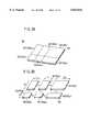
- FIG. 1shows an example a conventional QFP device 11 mounted upon a printed circuit board 14.
- the QFP device 11includes a resin package body 12 in which a semiconductor chip (not illustrated) is accommodated, wherein the QFP device 11 carries a number of lead pins 13 projecting laterally from the circumferential walls or side edges of the package body 12.
- the lead pins 13are bent in the downward direction outside the package body to form a well-known gull wing structure.
- the printed circuit board 14is formed of a material such as glass epoxy, and carries thereon a conductor pattern 15 in correspondence to the lead wires 13 of the QFP device 11 or other components, wherein the device 11 is mounted upon the substrate 14 by soldering the lead wires 13 upon the corresponding conductor patterns 15.
- a mounting processis used commonly in the art partly because of the fact that the soldering conducts easily due to the low reflow temperature of the solder alloy and partly because of the fact that glass epoxy substrate is easily available with a low cost.
- the semiconductor device 11includes a semiconductor chip encapsulated in the package body 12 formed of a resin, wherein the chip is held, inside the package body 12, on a lead frame stage as usual.
- the semiconductor chipcarries bonding pads thereon, and the bonding pads are interconnected to corresponding inner leads of the lead wires 13 by bonding wires.
- a so-called multi-chip module structurewherein a plurality of semiconductor chips are encapsulated in a single package body.
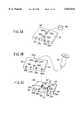
- FIGS. 2A-2Dshow the construction of a conventional multi-chip module in an elevational cross section.
- the multi-chip module 21Aincludes a chip mother board 22a carrying thereon a plurality of semiconductor chips 23, wherein the semiconductor chips 23 are connected electrically to the chip mother board 22a by means of bonding wires 24.
- the chip mother board 22aitself is held on a lead frame stage 25 and is connected electrically to inner leads 26a by the bonding wires 24.
- the semiconductor chips 23are encapsulated in a resin package body 27 together with the lead frame stage 25 and the chip mother board 22a as well as with the inner leads 26a, wherein outer leads 28a extend laterally from the package body 27 as an extension of the inner leads 26a.
- the outer leads 28aare thereby bent in the downward direction to form a J-shaped lead structure.
- FIG. 2Bshows another multi-chip module 21B that includes the semiconductor chips 23 in plural numbers on a chip mother board 22b, wherein the semiconductor chips 23 are connected electrically to the chip mother board 23b by means of the lead wires 24, similarly to the device 21A of FIG. 2A.
- the chip mother board 22bcarries thereon inner leads 26b directly such that the inner leads 26b are held upon a lower major surface of the chip mother board 22b together with the semiconductor chips 23.
- the semiconductor chips 23are thereby encapsulated in the resin package body 27 together with the chip mother board 22b and the inner leads 26b, and outer leads 28b extend laterally from the resin package body 27 as an extension of the inner leads 26b.
- the outer leads 28bare thereby bent in the downward direction outside the package body 27 to form a gull wing lead structure.
- FIG. 2Cshows a still other multi-chip module 21C, wherein the device 21C has a structure similar to that of the device 21B of FIG. 2B, except that the upper major surface of the chip mother board 22b is exposed for contact with a heat sink 29.
- FIG. 2Dshows a still other multi-chip module 21D, wherein the device 21D has a structure similar to that of FIG. 2B except that each of the semiconductor chips 23 carries thereon bumps 23a for mounting upon a corresponding tape lead by way of the flip-chip process.
- the semiconductor chips 23are mounted upon a corresponding tape lead 30 provided on the chip mother board 22b by the flip-chip process.
- the semiconductor chips 23are mounted upon both upper and lower major surfaces of the chip mother board 22b.
- FIGS. 2A-2DIn the case of the multi-chip modules 21A-21D of FIGS. 2A-2D, on the other hand, it should be noted that the interconnection between the semiconductor chips 23 and the chip mother board 22a or 22b is achieved by way of the bonding wire 24 or tape lead 30. Thus, such a conventional construction has a drawback of increased length of wiring and corresponding deterioration of the operational speed. Further, construction of FIGS. 2A-2D has another drawback in that it requires extensive modification of the interconnection or replacement of components when a design change has occurred in the multi-chip module. In such conventional multi-chip modules, therefore, such a design change inevitably invites substantial increase in the number of the fabrication steps and hence a corresponding increase in the fabrication cost of the device.
- Another and more specific object of the present inventionis to provide a low cost semiconductor device having a high operational speed.
- Another object of the present inventionis to provide a semiconductor device, comprising:
- a plurality of chip unitseach defined by a side wall and including a semiconductor chip, said plurality of chip units being arranged in a state such that a side wall of a chip unit abuts a corresponding side wall of an adjacent chip unit, in a flush manner each of said plurality of chip units including a plurality of terminals;
- interconnection meansfor interconnecting said plurality of terminals of a chip unit to corresponding terminals of an adjacent chip unit that abuts said chip unit at said respective side walls.
- the present inventionit is possible to construct a flat multi-chip module of high performance with a substantially reduced thickness. Further, such a multi-chip module allows easy replacement of the chip unit as necessary, even when there occurs a change in the design of the multi-chip module. Thereby, the fabrication cost of the semiconductor device is reduced. Further, the multi-chip module of the present invention eliminates use of interconnection wires or patterns and the operational speed of the device is maximized.
- FIG. 1is a diagram showing the construction of a conventional semiconductor device having the QFP structure
- FIGS. 2A-2Dare diagrams showing the structure of various conventional multi-chip modules
- FIGS. 3A and 3Bare diagrams showing the construction of a multi-chip module according to a first embodiment of the present invention respectively in a perspective view and an exploded view;
- FIGS. 4A and 4Bare diagrams showing the assembling process of the multi-chip module of the first embodiment of the present invention.
- FIGS. 5A-5Care diagrams showing various modifications of the multi-chip module of the first embodiment of the present invention.
- FIGS. 6A-6Care diagrams showing further modifications of the first embodiment
- FIGS. 7A-7Care diagrams showing the assembling of the multi-chip module of the first embodiment
- FIGS. 8A and 8Bare diagrams showing another example of assembling the multi-chip module of the first embodiment
- FIGS. 9A-9Dare diagrams showing other various modifications of the multi-chip module of the first embodiment.
- FIGS. 10A-10Dare diagrams showing various cooling schemes of the multi-chip module of the first embodiment
- FIGS. 11A-11Care diagrams showing the multi-chip module of the first embodiment that uses various chip mother boards;
- FIGS. 12A-12Care diagrams showing the multi-chip module of the first embodiment that uses other chip mother boards;
- FIGS. 13A-13Dare diagrams showing the fabrication process of the multi-chip module of the first embodiment
- FIG. 14is a diagram showing a modification of the fabrication process of the multi-chip module of the first embodiment
- FIG. 15is a diagram showing a further modification of the multi-chip module of the first embodiment
- FIGS. 16A and 16Bare diagrams showing a further modification of the multi-chip module of the first embodiment
- FIGS. 17A-17Dare diagrams showing further various modifications of the multi-chip module of the first embodiment.
- FIG. 18is a diagram showing the construction of a semiconductor device according to a second embodiment of the present invention.
- FIGS. 3A and 3Bshow the construction of a multi-chip module 31 according to a first embodiment of the present invention, wherein FIG. 3A shows the overall construction of the multi-chip module 31 while FIG. 3B shows the process of assembling the multi-chip module 31 of FIG. 3A.
- the multi-chip module 31includes a number of chip units 32 (32 1 -32 6 ) each having a rectangular shape, wherein the chip units 32 1 -32 6 are assembled in a two-dimensional plane to form together a flat body.
- the chip units 32are assembled such that a side edge of a chip unit, such as the chip unit 32 1 , abuts a corresponding side edge of adjacent chip unit such as the chip unit 32 2 or 32 3 .
- the chip units 32 1 -32 6are designed to perform various respective functions such as a memory function, arithmetic function, power supplying function, clock generation function, resistor function, capacitor function, and the like, and are formed of respective bare chips.
- the chip unit 32 1may act as a memory
- the chip unit 32 2may act as an arithmetic unit
- the chip unit 32 3may act as a power supply
- the chip unit 32 4may act as a clock generator
- the chip unit 32 5may act as a resistor
- the chip unit 32 6may act as a capacitor.
- each of the chip units 32 1 -32 6carries a plurality of terminals 33 on the side edges thereof such that the terminals 33 are exposed on the side edges.
- the chip units 32In the assembled state shown in FIG. 3A wherein the chip units 32 abut with each other at respective side edges, in a flush manner with no space between the respective side edges the terminals on a chip unit such as the chip unit 32 1 abuts respective, corresponding terminals on an adjacent chip unit such as the chip unit 32 2 .
- the chip units 32 forming the multi-chip module 31are electrically interconnected with each other.
- FIG. 3Bshows the multi-chip module 31 in an exploded view.
- each of the chip units 32 forming the multi-chip module 31has a rectangular shape with first and second, mutually intersecting side edges, wherein the first side edge is set to have a length of an integer multiple of a fundamental length a. Further, the second side edge is set to have a length equal to an integer multiple of another fundamental length b.
- the chip unit 32 5has a size of a ⁇ b
- the chip unit 32 1has a size of 2a ⁇ 2b
- the chip unit 32 6has a size of 2a ⁇ b
- the chip unit 32 3has a size of a ⁇ 2b.
- the terminals 33are formed by providing suitable electrode patterns on a wafer, followed by scribing along the scribe lines. As a result of scribing that divides the wafer into the individual chip units 32, the electrode patterns are exposed on the side edges of the chip units 32 as the terminals 33.
- the multi-chip module 31 of FIG. 3Ait should be noted that one can easily attend to the required design change by merely replacing one or more of the chip units 32. Thereby, the time needed for developing a new device is reduced substantially. Further, the multi-chip module 31 of FIG. 3A has an advantageous feature of increased operational speed, as the multi-chip module 31 eliminates the bonding wire or tape lead used in the conventional multi-chip modules for electrical connection.
- FIGS. 4A and 4Bshow the assembling of the multi-chip module 31 of FIG. 3A.
- the assembling of the multi-chip module 31is achieved by engaging the terminals 33 on the side edge of a chip unit such as the chip unit 32 3 , with the corresponding terminals 33 provided on the respective side edges of the chip units 32 1 and 32 4 .
- FIG. 4Bshows the details of the assembling process of FIG. 4A.
- a sheet 34 carrying a number of conductor pads 34a thereonis disposed between the terminals 33 of the chip unit 32 3 and the terminals 33 of the chip unit 32 4 .
- the terminals 33 of the chip unit 32 3are connected electrically to the corresponding terminals 33 of the chip unit 32 4 via the conductor pads 34a.
- the conductor pad 34aconnects only the terminals 33 that oppose with each other across the sheet 34.
- FIGS. 5A-5Cshow another examples of connecting the chip units 32 with each other, wherein FIG. 5A shows a case wherein each of the chip units 32 has terminals 33a on the side edges thereof such that each terminal 33a has a circular cutout or depression that increases the size in the interior of the chip unit. Thereby, two such circular cutouts form together a dumbbell shaped cutout when a chip unit 32 and another chip unit 32 are assembled with each other in the state that the respective side edges abut with each other.
- the dumbbell shaped cutoutis filled by a corresponding dumbbell shaped conductor element 35 that achieves not only the electrical connection between the two terminals 33a but also a mechanical connection of the two adjacent chip units 32.
- FIG. 5Bshows an example wherein each of the chip units 32 carries a plurality of terminals 33b along the side edge of the chip unit in the form of a cutout provided at the upper corner of the foregoing side edge.
- the terminals 33b of the two adjacent chip units 32form together a depression when the two chip units 32 are abutted with each other at the respective side walls.
- FIG. 5Cshows a case in which terminal pads 33c are formed on the upper major surface of the chip unit 32.
- the chip units 32are assembled to form a flat body similarly as before, wherein the terminal pads 33c on the upper major surface of the chip units are connected with each other by bonding wires 37.
- the bonding wire 37By using the bonding wire 37, it becomes also possible to connect the chip units 32 that do not contact with each other, although such a wire bonding provides a slight delay in signal processing due to the increased length of the bonding wire. Even so, the construction of the present invention provides a much higher processing speed as compared with the conventional multi-chip module shown in FIGS. 2A-2D.
- the terminalssuch as the terminals 33. 33a, 33b or 33c, are connected to external conductor patterns on the printed circuit board either directly or via suitable socket means.
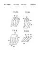
- FIGS. 6A-6Cshow other examples of the chip unit of the present invention.
- the chip units 32ahas a triangular shape and reduces the size of the multi-chip module 31 over the multi-chip module that uses the chip unit 32, depending on the number of the chip units used. It should be noted that such triangular chip units 32a can be formed easily by conventional wafer processing technology.
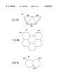
- FIG. 6Bshows a case wherein the multi-chip module 31 is formed of hexagonal chip units 32b.
- hexagonal chip units 32bBy using such hexagonal chip units 32b, it is possible to increase the area of contact with adjacent chip units, and the interconnection with other chip units is facilitated.
- the shape of the chip unitis not limited to triangular or hexagonal as set forth above, but other shapes such as octagonal shape is also possible.
- the size of the edgehas to be set to be an integer multiple of a predetermined size.
- FIG. 6Cshows a case in which the multi-chip module 31 is formed of circular chip units 32c, wherein each of the circular chip units 32c has a flat edge 32c 1 similar to the one provided on a semiconductor wafer, wherein two such circular chip units 32c are contacted with each other at the flat edge 32c 1 .
- the chip units 32 each carrying the terminals 33 on the side edges thereofare mounted upon a chip mother board 38 that carries thereon interconnection pads 39 that act also as a point of mechanical connection, wherein the pads 39 are formed with number and pitch corresponding to the number and pitch of the terminals 33 on the chip units 32 as well as the terminals for external connection.
- the interconnection of the terminals 33 on the chip units 32 and the pads 39 on the chip mother board 38is achieved by applying a laser beam to the contacting part of the terminal 33 and the pad 39 to cause a reflowing.
- solder alloys or conductive resinssuch as silver paste.
- Such a constructionis advantageous in the point that the chip units 32 can be easily dismounted by heating or by applying a laser beam whenever there arises a need for replacing the chip unit 32. As a result, one obtains a flat structure for the multi-chip module 31 as indicated in FIG. 7B.
- Such a flat multi-chip module 31is suitable for handling by an automatic transport system as indicated in FIG. 7C.
- the automatic transport systemincludes a suction unit 41 on a tip end of an arm 42, wherein the suction unit 41 includes a suction pad 43 that is evacuated via a tube 44. Thereby, the suction pad 43 engages firmly upon the upper major surface of the flat multi-chip module 31 and carries the same as necessary.
- the external connection of the multi-chip module 31is achieved as necessary by suitable means such as a connector or wire.
- suitable meanssuch as a connector or wire.
- BGAball grid array
- FIGS. 8A and 8Bshow another example of mounting the chip units 32 upon the chip mother board 38.
- the chip mother board 38is formed with a number of through holes 40 along the edge of the chip assembly, which chip assembly being formed of the chip units 32 arranged side by side, with a pitch d corresponding to the pitch of the terminals 33 on the side wall of the chip assembly.
- each chip 32carries the terminals 33 along the lower edge of the side walls such that each terminal 33 contacts with a conductive sleeve 40a provided in the corresponding through hole 40.
- the terminals 33cause a fusion and establishes a firm mechanical as well as electrical contact with the sleeves 40a of the through holes 40.
- FIGS. 9A-9Dshow the case of mounting the chip units 32 generally vertically upon the chip mother board 38.
- each of the chip units 32is mounted upon the chip mother board 38 substantially vertically such that an edge of the chip unit 32 abuts with the chip mother board 38.
- the area of contact of the chip units 32 and the chip mother board 38is substantially reduced, and the heat transfer from the chip units 32 to the mother board 38 is accordingly reduced.
- FIG. 9Bshows a modification of FIG. 9A, wherein another chip unit 32 7 is mounted upon the chip unit 32 2 by way of solder bumps 51.
- Such a constructionis useful for example is a memory unit for increasing the memory capacity by adding extra memory unit by way of the chip unit 32 7 .
- FIG. 9Cshows a modification of FIG. 9A wherein another chip unit 52 is provided so as to bridge across the memory units 32 that are held vertically on the chip mother board 38.
- the chip unit 52abuts the exposed side edges of the chip units 32, and it is possible to achieve electrical connection between various of the chip units 32 on the chip mother board 38.
- the chip unit 52can be provided also on other side edges of the chip units 32.
- FIG. 9Dshows a modification of FIG. 9A wherein the chip units 52 are provided on the chip mother board 38 obliquely. According to the construction of FIG. 9D, it is possible to reduce the height of the multi-chip module 31.
- FIGS. 10A-10Dshow the cooling of the multi-chip module 31 of the present invention.
- the multi-chip module 31carries four chip units 32 on the chip mother board 38 to form a flat arrangement, wherein there is provided another chip mother board 38a that carries thereon another chip unit 32 8 .
- the chip unit 32 8 and the chip unit 32are connected with each other by bonding wires 37, wherein it will be noted that there is disposed a cooling pipe 53 between the chip mother board 38 and the chip mother board 38a for cooling the same by the air or a fluid passing through the cooling pipe 53.
- Such a constructionis particularly useful for isolating the chip mother board 38 from the other chip mother board 38a thermally or vice versa, such that the heating in one of the chip mother boards does not cause influence in the other chip mother board.
- two chip mother boards 38 and 38arather than using a single chip mother board, it is possible to enhance the effect of cooling even when the cooling by means of the cooling pipe 53 is not employed.
- FIG. 10Bshows a construction in which a heat radiation element 54 is provided at a suitable location of the multi-chip module 31 in which a plurality of chip units 32 are assembled on the chip mother board 38 to form a flat structure.
- the chip units 32are formed to as to expose the region of the chip mother board 38 on which the heat radiation element 54 is provided.
- the heat radiation element 54it is possible to enhance the efficiency of heat dissipation of the multi-chip module 31.
- FIG. 10Cshows a structure wherein a cooling fan 55 is provided on the rear side of the chip mother board 38.
- the cooling fan 55may be the one that moves freely with the cooling air, or the one that includes a drive motor. In any of these examples, the efficiency of cooling is further enhanced.
- FIG. 10Dshows an example wherein the multi-chip module 31 as a whole is immersed in a bath 55a of liquid nitrogen. As a result of cooling by the liquid nitrogen bath, it is possible to maximize the operational speed of the chip units 32 on the chip mother board 38 by minimizing the size of the multi-chip module 31 and hence by maximizing the integration density in the chip units 32.
- the multi-chip module 31is constructed upon a chip mother board 38b of a layered structure, wherein the chip mother board 38b carries thereon the chip units 32 on both the upper and lower major surfaces thereof.
- the electrical interconnection between the chip units 32is achieved by a wiring pattern 56 that is formed integrally with the layered chip mother board 38b.
- the wiring pattern 56establishes a contact with the terminals at the side edges of the chip units 32, wherein the wiring pattern 56 forms a part of the layered structure of the chip mother board 38b.
- FIG. 11Bshows a construction of the multi-chip module 31 that uses a hollow chip mother board 38c.
- the chip mother board 38cincludes a wiring pattern as indicated by the pattern 56, wherein the wiring pattern 56 is formed integrally with the layered structure of the chip mother board 38c, similarly to the construction of FIG. 11A.
- the chip mother board 38c of FIG. 11Bincludes a hollow space 57 communicating with the exterior via an opening 57a, wherein there are formed a number of openings 57b in the interior of the hollow space 57 so as to expose the lower major surface of the chip units 32.
- the openings 57b thus formedact as a vent that allows the cooling air introduced into the hollow space 57 via the passage 57a to contact with the exposed lower major surface of the chip units 32.
- the chip units 32are cooled from the rear side of the chip mother board 38c.
- FIG. 11Bit should be noted that one can employ the cooling construction described already with reference to FIG. 10A or FIG. 10B. Further, it is not necessary to provide the chip units 32 on both sides of the chip mother board 38c. One may provide the chip units 32 on only one side of the chip mother board 38c.
- FIG. 11Cshows an example of the multi-chip module that uses a flexible film 38d as the chip mother board.
- the flexible film 38dcarries thereon a conductor pattern 56a, and the conductor pattern 56a achieves an interconnection between a first block of the chip units 32 and a second block of the chip units 32, each of the first and second blocks including a plurality to chip units 32.
- the chip mother board 38dis formed of a polyimide film or a polyester film
- the conductor pattern 56ais formed of a copper foil provided on the foregoing plastic film.
- the construction of FIG. 11Callows free bending of the chip mother board and can used in a limited space.
- FIG. 12Ashows an example of the multi-chip module 31 similar to the construction of FIG. 7B, except that two holes 58 are formed in respective corners of the chip mother board 38 that is not occupied by the chip units 32. By providing such holes 58, it is possible to discriminate the orientation of the module 31. Thereby, a proper positioning or alignment of the chip units 32 becomes possible when carrying the multi-chip module 31 or mounting the same upon a printed circuit board.
- FIG. 12Bshows another example of providing a positioning part on the multi-chip module 31.
- a rod 59is provided on the rear side of the chip mother board 38 for the purpose of positioning.
- FIG. 12Cshows an example of the multi-chip module 31 in which a number of openings 60 are formed on the chip mother board 38 in correspondence to the chip units 32.
- the chip unit 32is easily dismounted by pressing the chip unit 32 via the opening 60 while holding the multi-chip module 31 at an elevated temperature such that the solder alloy used for mounting the chip units 32 upon the chip mother board 38 causes a reflow.
- a wafer 61 on which desired device patterns such as the device patterns of a memory circuit are formedis prepared according to the usual wafer process, followed by a scribing process conducted along scribe lines 62 that separates individual device patterns on the wafer 61.
- the scribingmay be conducted by suitable mechanical means such as a dicing saw.
- the wafer 61is subjected to exposure to a laser beam, before the scribing process, as indicated in FIG. 13A by a two-dotted arrow, such that the defective pattern is eliminated as a result of irradiation of the laser beam.
- a depression 33c 1As a result of irradiation of the laser beam, there is formed a depression 33c 1 as represented in FIG. 13B. Further, a conductive pattern is provided in correspondence to the depression 33c 1 by filling the depression by conductive member 33c 2 such as a silver paste or solder alloy as indicated in FIG. 13C.
- Such a mending processmay be repeated as necessary by irradiation the wafer 61 again by a laser beam as indicated in FIG. 13C.
- each of the chip units 32is formed of a bare chip.
- FIGS. 13A-13Dare useful not only for mending but also for forming the terminals 33 at the side edge of the chip unit 32.
- depression 33c 1 of FIG. 13Bis formed on the scribe lines 62 such that the conductive member 33c 3 filling depression 33c 1 is exposed at the side edge of the chip unit 32 upon the scribing of the wafer 61 into individual chip units 32.
- FIG. 14shows an alternative process of forming the depression 33c 1 on the surface of the wafer 61.
- the upper major surface of the wafer 61is subjected to grinding by means of a rotating dicing blade 63.
- the depression 33c 1thus formed by the conductive member 33c 2 , it is possible to provide the terminal pads on any of the upper major surface and the side edge of the chip units 32 as desired.
- FIG. 15shows the assembling of the chip units 32 each carrying the terminal pads 32c on the upper major surface for external connection, on the chip mother board 38 to form the multi-chip module 31.
- the chip units 32are interconnected with each other by the terminals 33 on the side edges that abut with each other as the chip units 32 are held on the chip mother board 38 such that the side edges thereof are abutted with each other.
- the chips 32are held on the chip mother board 38 with an intervening shock absorbing layer 64.
- a flexible resinsuch as urethane rubber or a metal leaf spring is used for the layer 64.
- the interconnection between the chip mother board 38 and the chip units 32is achieved by the bonding wires 37a that connects the terminal pads 33c formed on the chip units 32.
- the terminal pads 33cBy forming the terminal pads 33c according to the process of FIGS. 13A-13D or FIG. 14 according to the needs that may change device by device, it is possible to form only the terminals 33 that are necessary for device connection. Thereby, the risk pertinent to the conventional multi-chip module that carries unnecessary terminals on the chip units 32 for general use of the chip unit, that moisture may penetrate into the chip unit 32 via the terminals is substantially reduced. Thereby, the reliability as well as yield of the device is improved substantially.
- FIGS. 16A and 16Bshow the examples of the multi-chip module 31 that has a protective member, wherein FIG. 16A shows the module 31 in a perspective view while FIG. 16B shows the module 31 in a cross sectional view.
- the multi-chip module 31includes a protective member 65a that surrounds the chip units 32 hold on the chip mother board 38, wherein the chip mother board 38 carries a predetermine number of the chip units 32 thereon similarly as before.
- the protective member 65ais typically formed of a metal or resin and protects the chip units 32 from external shocks.
- FIGS. 17A-17Dshow other examples of the multi-chip module 31 that carries a protective member, wherein FIG. 17A shows an example in which a protective member 65b formed of a resin is coated upon the chip units 32 held on the chip mother board 38.
- FIG. 17Bshows an example in which the chip units 32 are disposed on the chip mother board 38 such that the chip units 32 are accommodated in a space formed inside a resin or metal protective member 65c.
- the multi-chip module 31uses a chip mother board 38e having a depression at a central part thereof, wherein the chip units 32 forming the multi-chip module 31 are accommodated in the central depression on the chip mother board 38e.
- the central depressionis surrounded laterally by a side wall, and the side wall carries a screw thread 38e 1 on an outer surface thereof.
- a cap member 65d of resin or metalthat has a side wall on which a thread 65d 1 that mates the thread 38e 1 is formed.
- FIG. 17Dshows another example of the multi-chip module 31 that uses a chip mother board 38f, wherein the chip mother board 38f includes a depression for holding the chip units 32.
- the chip units 32are surrounded laterally by a side wall of the chip mother board 38f, and a cap member 65e of resin or metal is placed upon the chip mother board 38 such that the cap member 65e and the chip mother board 38f form together a space in which the chip units 32 are accommodated, wherein the side wall of the chip mother board 38f carries on the outer surface thereof a seal ring 66 that seals the gap between the outer surface of the side wall of the chip mother board 38f and the corresponding inner surface of the cap member 65e.
- the interior of the space in which the chip units 32 are accommodatedis held in an airtight state.
- FIG. 18shows a semiconductor device 71 according to a second embodiment of the present invention.
- the semiconductor device 71includes a plurality of multi-chip modules each having a construction of the multi-chip module 31, wherein the multi-chip modules are held parallel with each other between a pair of mother boards 72a and 72b.
- the bother boards 72a and 72bprovides an electrical interconnection between different multi-chip modules.
- each of the multi-chip modules 31includes the chip units 32 that are interconnected with each other by the terminals at the respective side edges. Such a construction is useful in reducing the overall size of the semiconductor device. Further, replacement of the chip units 32 is achieved easily in such a construction whenever there is a need for the replacement of a chip unit 32.
Landscapes
- Engineering & Computer Science (AREA)
- Power Engineering (AREA)
- Microelectronics & Electronic Packaging (AREA)
- Physics & Mathematics (AREA)
- Condensed Matter Physics & Semiconductors (AREA)
- General Physics & Mathematics (AREA)
- Computer Hardware Design (AREA)
- Wire Bonding (AREA)
- Cooling Or The Like Of Semiconductors Or Solid State Devices (AREA)
Abstract
Description
Claims (25)
Priority Applications (1)
| Application Number | Priority Date | Filing Date | Title |
|---|---|---|---|
| US09/145,027US6287949B1 (en) | 1994-06-20 | 1998-09-01 | Multi-chip semiconductor chip module |
Applications Claiming Priority (2)
| Application Number | Priority Date | Filing Date | Title |
|---|---|---|---|
| JP6-137608 | 1994-06-20 | ||
| JP13760894AJP3519453B2 (en) | 1994-06-20 | 1994-06-20 | Semiconductor device |
Related Child Applications (1)
| Application Number | Title | Priority Date | Filing Date |
|---|---|---|---|
| US09/145,027DivisionUS6287949B1 (en) | 1994-06-20 | 1998-09-01 | Multi-chip semiconductor chip module |
Publications (1)
| Publication Number | Publication Date |
|---|---|
| US5834843Atrue US5834843A (en) | 1998-11-10 |
Family
ID=15202669
Family Applications (2)
| Application Number | Title | Priority Date | Filing Date |
|---|---|---|---|
| US08/427,111Expired - LifetimeUS5834843A (en) | 1994-06-20 | 1995-04-21 | Multi-chip semiconductor chip module |
| US09/145,027Expired - LifetimeUS6287949B1 (en) | 1994-06-20 | 1998-09-01 | Multi-chip semiconductor chip module |
Family Applications After (1)
| Application Number | Title | Priority Date | Filing Date |
|---|---|---|---|
| US09/145,027Expired - LifetimeUS6287949B1 (en) | 1994-06-20 | 1998-09-01 | Multi-chip semiconductor chip module |
Country Status (2)
| Country | Link |
|---|---|
| US (2) | US5834843A (en) |
| JP (1) | JP3519453B2 (en) |
Cited By (36)
| Publication number | Priority date | Publication date | Assignee | Title |
|---|---|---|---|---|
| US6262434B1 (en)* | 1996-08-23 | 2001-07-17 | California Micro Devices Corporation | Integrated circuit structures and methods to facilitate accurate measurement of the IC devices |
| WO2001099189A1 (en)* | 2000-06-19 | 2001-12-27 | Advantest Corporation | Method and apparatus for edge connection between elements of an integrated circuit |
| US6369445B1 (en)* | 2000-06-19 | 2002-04-09 | Advantest Corporation | Method and apparatus for edge connection between elements of an integrated circuit |
| US20020053040A1 (en)* | 2000-11-02 | 2002-05-02 | Kazuyuki Kikuchi | Semiconductor integrated device |
| US20020117753A1 (en)* | 2001-02-23 | 2002-08-29 | Lee Michael G. | Three dimensional packaging |
| US6465858B2 (en)* | 2000-03-24 | 2002-10-15 | Matsushita Electric Industrial Co., Ltd. | Semiconductor device package for optical communication device |
| US6469901B1 (en)* | 2000-05-15 | 2002-10-22 | 3C Interactive, Inc. | System and method for cartridge-based, geometry-variant scalable electronic systems |
| DE10130592C1 (en)* | 2001-06-27 | 2002-10-24 | Infineon Technologies Ag | Module component used for storage modules for data processing comprises a main module and sub-modules |
| US6492720B1 (en)* | 2001-06-06 | 2002-12-10 | Mitsubishi Denki Kabushiki Kaisha | Flat-type semiconductor stack |
| US20020190367A1 (en)* | 2001-06-15 | 2002-12-19 | Mantz Frank E. | Slice interconnect structure |
| US20030002267A1 (en)* | 2001-06-15 | 2003-01-02 | Mantz Frank E. | I/O interface structure |
| US20030001257A1 (en)* | 1998-07-09 | 2003-01-02 | Masao Jojiki | Semiconductor device and semiconductor assembly apparatus for semiconductor device |
| US6512293B1 (en)* | 2001-06-05 | 2003-01-28 | Lsi Logic Corporation | Mechanically interlocking ball grid array packages and method of making |
| US20030051911A1 (en)* | 2001-09-20 | 2003-03-20 | Roeters Glen E. | Post in ring interconnect using 3-D stacking |
| US6573461B2 (en) | 2001-09-20 | 2003-06-03 | Dpac Technologies Corp | Retaining ring interconnect used for 3-D stacking |
| US6717245B1 (en)* | 2000-06-02 | 2004-04-06 | Micron Technology, Inc. | Chip scale packages performed by wafer level processing |
| US6716670B1 (en) | 2002-01-09 | 2004-04-06 | Bridge Semiconductor Corporation | Method of forming a three-dimensional stacked semiconductor package device |
| US20040108584A1 (en)* | 2002-12-05 | 2004-06-10 | Roeters Glen E. | Thin scale outline package |
| US20040207990A1 (en)* | 2003-04-21 | 2004-10-21 | Rose Andrew C. | Stair-step signal routing |
| US20040245654A1 (en)* | 2003-06-03 | 2004-12-09 | Liu Shuan Ta | Flip-chip attach structure and method |
| US20050023675A1 (en)* | 2003-06-23 | 2005-02-03 | Sanyo Electric Co., Ltd. | Semiconductor device and manufacturing method of the same |
| GB2409072A (en)* | 2003-12-09 | 2005-06-15 | Optimum Care Int Tech Inc | Memory module comprising units jointed together by tabs and sockets along the sides each holding a chip |
| US6936495B1 (en) | 2002-01-09 | 2005-08-30 | Bridge Semiconductor Corporation | Method of making an optoelectronic semiconductor package device |
| US6987034B1 (en) | 2002-01-09 | 2006-01-17 | Bridge Semiconductor Corporation | Method of making a semiconductor package device that includes singulating and trimming a lead |
| US20070018335A1 (en)* | 2005-07-11 | 2007-01-25 | Samsung Electro-Mechanics Co., Ltd. | Polygonal, rounded, and circular flip chip ball grid array board |
| US7190060B1 (en) | 2002-01-09 | 2007-03-13 | Bridge Semiconductor Corporation | Three-dimensional stacked semiconductor package device with bent and flat leads and method of making same |
| US7203074B1 (en)* | 2003-07-28 | 2007-04-10 | Intellect Lab, Llc | Electronic circuit building block |
| US20080017971A1 (en)* | 2006-07-21 | 2008-01-24 | Bae Systems Information And Electronic Systems Integration Inc. | High speed, high density, low power die interconnect system |
| US20080174023A1 (en)* | 2007-01-23 | 2008-07-24 | Samsung Electronics Co., Ltd. | Chip having side pad, method of fabricating the same and package using the same |
| US20080273424A1 (en)* | 2007-05-02 | 2008-11-06 | Robert Gideon Wodnicki | Monitoring or imaging system with interconnect structure for large area sensor array |
| US20080315331A1 (en)* | 2007-06-25 | 2008-12-25 | Robert Gideon Wodnicki | Ultrasound system with through via interconnect structure |
| EP1737039A3 (en)* | 2005-06-23 | 2009-07-29 | Nokia Corporation | Semiconductor Package |
| US9099363B1 (en)* | 2014-02-12 | 2015-08-04 | Freescale Semiconductor, Inc. | Substrate with corner cut-outs and semiconductor device assembled therewith |
| US20160013159A1 (en)* | 2014-07-08 | 2016-01-14 | Jong-oh Kwon | Chip, chip-stacked package using the same, and method of manufacturing the chip-stacked package |
| US9911716B2 (en) | 2015-01-29 | 2018-03-06 | International Business Machines Corporation | Polygon die packaging |
| US11410894B2 (en) | 2019-09-06 | 2022-08-09 | International Business Machines Corporation | Polygon integrated circuit (IC) packaging |
Families Citing this family (40)
| Publication number | Priority date | Publication date | Assignee | Title |
|---|---|---|---|---|
| US7805756B2 (en) | 1996-11-29 | 2010-09-28 | Frampton E Ellis | Microchips with inner firewalls, faraday cages, and/or photovoltaic cells |
| US7634529B2 (en) | 1996-11-29 | 2009-12-15 | Ellis Iii Frampton E | Personal and server computers having microchips with multiple processing units and internal firewalls |
| US8225003B2 (en) | 1996-11-29 | 2012-07-17 | Ellis Iii Frampton E | Computers and microchips with a portion protected by an internal hardware firewall |
| US7926097B2 (en) | 1996-11-29 | 2011-04-12 | Ellis Iii Frampton E | Computer or microchip protected from the internet by internal hardware |
| US8312529B2 (en) | 1996-11-29 | 2012-11-13 | Ellis Frampton E | Global network computers |
| US20050180095A1 (en)* | 1996-11-29 | 2005-08-18 | Ellis Frampton E. | Global network computers |
| US6725250B1 (en) | 1996-11-29 | 2004-04-20 | Ellis, Iii Frampton E. | Global network computers |
| US7506020B2 (en) | 1996-11-29 | 2009-03-17 | Frampton E Ellis | Global network computers |
| US6167428A (en)* | 1996-11-29 | 2000-12-26 | Ellis; Frampton E. | Personal computer microprocessor firewalls for internet distributed processing |
| US7024449B1 (en)* | 1996-11-29 | 2006-04-04 | Ellis Iii Frampton E | Global network computers |
| US6127245A (en)* | 1997-02-04 | 2000-10-03 | Micron Technology, Inc. | Grinding technique for integrated circuits |
| US6664628B2 (en)* | 1998-07-13 | 2003-12-16 | Formfactor, Inc. | Electronic component overlapping dice of unsingulated semiconductor wafer |
| US6696765B2 (en)* | 2001-11-19 | 2004-02-24 | Hitachi, Ltd. | Multi-chip module |
| US6610560B2 (en)* | 2001-05-11 | 2003-08-26 | Siliconware Precision Industries Co., Ltd. | Chip-on-chip based multi-chip module with molded underfill and method of fabricating the same |
| US6791035B2 (en)* | 2002-02-21 | 2004-09-14 | Intel Corporation | Interposer to couple a microelectronic device package to a circuit board |
| US7612443B1 (en) | 2003-09-04 | 2009-11-03 | University Of Notre Dame Du Lac | Inter-chip communication |
| US7705464B2 (en)* | 2004-09-13 | 2010-04-27 | Taiwan Semiconductor Manufacturing Company, Ltd. | Connection structure for semiconductor devices |
| KR100771862B1 (en)* | 2005-08-12 | 2007-11-01 | 삼성전자주식회사 | Printed circuit board, manufacturing method and memory module-socket assembly for memory module |
| US7750441B2 (en)* | 2006-06-29 | 2010-07-06 | Intel Corporation | Conductive interconnects along the edge of a microelectronic device |
| DE102006033870B4 (en)* | 2006-07-21 | 2009-02-26 | Infineon Technologies Ag | Electronic component with a plurality of substrates and a method for producing the same |
| JP2008047802A (en)* | 2006-08-21 | 2008-02-28 | Nec Electronics Corp | Semiconductor device and production method therefor |
| US8193613B2 (en)* | 2007-03-06 | 2012-06-05 | Broadcom Corporation | Semiconductor die having increased usable area |
| US8125796B2 (en) | 2007-11-21 | 2012-02-28 | Frampton E. Ellis | Devices with faraday cages and internal flexibility sipes |
| US7928563B2 (en)* | 2008-05-28 | 2011-04-19 | Georgia Tech Research Corporation | 3-D ICs with microfluidic interconnects and methods of constructing same |
| US8546930B2 (en)* | 2008-05-28 | 2013-10-01 | Georgia Tech Research Corporation | 3-D ICs equipped with double sided power, coolant, and data features |
| US8283566B2 (en)* | 2009-03-14 | 2012-10-09 | Palo Alto Research Center Incorporated | Printed circuit boards by massive parallel assembly |
| US12401619B2 (en) | 2010-01-26 | 2025-08-26 | Frampton E. Ellis | Computer or microchip with a secure system bios having a separate private network connection to a separate private network |
| US8429735B2 (en) | 2010-01-26 | 2013-04-23 | Frampton E. Ellis | Method of using one or more secure private networks to actively configure the hardware of a computer or microchip |
| US8541262B2 (en)* | 2010-09-02 | 2013-09-24 | Taiwan Semiconductor Manufacturing Company, Ltd. | Die edge contacts for semiconductor devices |
| US9190371B2 (en)* | 2010-12-21 | 2015-11-17 | Moon J. Kim | Self-organizing network with chip package having multiple interconnection configurations |
| CN102779760B (en)* | 2011-05-13 | 2015-06-03 | 力成科技股份有限公司 | Process and Structure of Mounted Substrate Multi-die Package |
| USD668658S1 (en)* | 2011-11-15 | 2012-10-09 | Connectblue Ab | Module |
| USD668659S1 (en)* | 2011-11-15 | 2012-10-09 | Connectblue Ab | Module |
| USD680545S1 (en)* | 2011-11-15 | 2013-04-23 | Connectblue Ab | Module |
| USD689053S1 (en)* | 2011-11-15 | 2013-09-03 | Connectblue Ab | Module |
| USD680119S1 (en)* | 2011-11-15 | 2013-04-16 | Connectblue Ab | Module |
| USD692896S1 (en)* | 2011-11-15 | 2013-11-05 | Connectblue Ab | Module |
| US9620473B1 (en) | 2013-01-18 | 2017-04-11 | University Of Notre Dame Du Lac | Quilt packaging system with interdigitated interconnecting nodules for inter-chip alignment |
| US10923456B2 (en)* | 2018-12-20 | 2021-02-16 | Cerebras Systems Inc. | Systems and methods for hierarchical exposure of an integrated circuit having multiple interconnected die |
| CN112448561B (en) | 2019-08-30 | 2022-04-15 | 台达电子企业管理(上海)有限公司 | Power module and preparation method thereof |
Citations (3)
| Publication number | Priority date | Publication date | Assignee | Title |
|---|---|---|---|---|
| US4860444A (en)* | 1986-03-31 | 1989-08-29 | Microelectronics And Computer Technology Corporation | Method of assembling a fluid-cooled integrated circuit package |
| US4990462A (en)* | 1989-04-12 | 1991-02-05 | Advanced Micro Devices, Inc. | Method for coplanar integration of semiconductor ic devices |
| US5406027A (en)* | 1990-11-26 | 1995-04-11 | Hitachi, Ltd. | Mounting structure and electronic device employing the same |
Family Cites Families (7)
| Publication number | Priority date | Publication date | Assignee | Title |
|---|---|---|---|---|
| US6379998B1 (en)* | 1986-03-12 | 2002-04-30 | Hitachi, Ltd. | Semiconductor device and method for fabricating the same |
| JPS6427420A (en) | 1987-07-22 | 1989-01-30 | Matsushita Electric Industrial Co Ltd | Hydroponic culture apparatus |
| US5126286A (en)* | 1990-10-05 | 1992-06-30 | Micron Technology, Inc. | Method of manufacturing edge connected semiconductor die |
| US5272113A (en)* | 1992-11-12 | 1993-12-21 | Xerox Corporation | Method for minimizing stress between semiconductor chips having a coefficient of thermal expansion different from that of a mounting substrate |
| KR100245257B1 (en)* | 1993-01-13 | 2000-02-15 | 윤종용 | Manufacturing method of semiconductor package at wafer level |
| JP3147666B2 (en)* | 1994-07-21 | 2001-03-19 | 株式会社村田製作所 | Multilayer electronic component and method of manufacturing the same |
| MY114888A (en)* | 1994-08-22 | 2003-02-28 | Ibm | Method for forming a monolithic electronic module by stacking planar arrays of integrated circuit chips |
- 1994
- 1994-06-20JPJP13760894Apatent/JP3519453B2/ennot_activeExpired - Lifetime
- 1995
- 1995-04-21USUS08/427,111patent/US5834843A/ennot_activeExpired - Lifetime
- 1998
- 1998-09-01USUS09/145,027patent/US6287949B1/ennot_activeExpired - Lifetime
Patent Citations (3)
| Publication number | Priority date | Publication date | Assignee | Title |
|---|---|---|---|---|
| US4860444A (en)* | 1986-03-31 | 1989-08-29 | Microelectronics And Computer Technology Corporation | Method of assembling a fluid-cooled integrated circuit package |
| US4990462A (en)* | 1989-04-12 | 1991-02-05 | Advanced Micro Devices, Inc. | Method for coplanar integration of semiconductor ic devices |
| US5406027A (en)* | 1990-11-26 | 1995-04-11 | Hitachi, Ltd. | Mounting structure and electronic device employing the same |
Cited By (78)
| Publication number | Priority date | Publication date | Assignee | Title |
|---|---|---|---|---|
| US6262434B1 (en)* | 1996-08-23 | 2001-07-17 | California Micro Devices Corporation | Integrated circuit structures and methods to facilitate accurate measurement of the IC devices |
| US6841417B2 (en)* | 1998-07-09 | 2005-01-11 | Asahi Kogaku Kogyo Kabushiki Kaisha | Semiconductor device and semiconductor assembly apparatus for semiconductor device |
| US20030001257A1 (en)* | 1998-07-09 | 2003-01-02 | Masao Jojiki | Semiconductor device and semiconductor assembly apparatus for semiconductor device |
| US6465858B2 (en)* | 2000-03-24 | 2002-10-15 | Matsushita Electric Industrial Co., Ltd. | Semiconductor device package for optical communication device |
| US6469901B1 (en)* | 2000-05-15 | 2002-10-22 | 3C Interactive, Inc. | System and method for cartridge-based, geometry-variant scalable electronic systems |
| US20070148918A1 (en)* | 2000-06-02 | 2007-06-28 | Kinsman Larry D | Method for fabricating a chip scale package using wafer level processing |
| US20040126928A1 (en)* | 2000-06-02 | 2004-07-01 | Kinsman Larry D. | Method for fabricating a chip scale package using wafer level processing and devices resulting therefrom |
| US7727858B2 (en) | 2000-06-02 | 2010-06-01 | Micron Technology, Inc. | Method for fabricating a chip scale package using wafer level processing |
| US6717245B1 (en)* | 2000-06-02 | 2004-04-06 | Micron Technology, Inc. | Chip scale packages performed by wafer level processing |
| US7183191B2 (en) | 2000-06-02 | 2007-02-27 | Micron Technology, Inc. | Method for fabricating a chip scale package using wafer level processing |
| US6780746B2 (en) | 2000-06-02 | 2004-08-24 | Micron Technology, Inc. | Method for fabricating a chip scale package using wafer level processing and devices resulting therefrom |
| US20050164429A1 (en)* | 2000-06-02 | 2005-07-28 | Kinsman Larry D. | Method for fabricating a chip scale package using wafer level processing |
| US6900079B2 (en) | 2000-06-02 | 2005-05-31 | Micron Technology, Inc. | Method for fabricating a chip scale package using wafer level processing |
| US6369445B1 (en)* | 2000-06-19 | 2002-04-09 | Advantest Corporation | Method and apparatus for edge connection between elements of an integrated circuit |
| CN1305181C (en)* | 2000-06-19 | 2007-03-14 | 株式会社鼎新 | Connecting component and its assembling mechanism |
| WO2001099189A1 (en)* | 2000-06-19 | 2001-12-27 | Advantest Corporation | Method and apparatus for edge connection between elements of an integrated circuit |
| SG90252A1 (en)* | 2000-06-19 | 2002-07-23 | Advantest Corp | Contact structure and assembly mechanism thereof |
| US6440775B2 (en) | 2000-06-19 | 2002-08-27 | Advantest Corporation | Method and apparatus for edge connection between elements of an integrated circuit |
| US20020053040A1 (en)* | 2000-11-02 | 2002-05-02 | Kazuyuki Kikuchi | Semiconductor integrated device |
| US6948137B2 (en)* | 2000-11-02 | 2005-09-20 | Renesas Technology Corp. | Semiconductor integrated device |
| US20020117753A1 (en)* | 2001-02-23 | 2002-08-29 | Lee Michael G. | Three dimensional packaging |
| US6512293B1 (en)* | 2001-06-05 | 2003-01-28 | Lsi Logic Corporation | Mechanically interlocking ball grid array packages and method of making |
| US6492720B1 (en)* | 2001-06-06 | 2002-12-10 | Mitsubishi Denki Kabushiki Kaisha | Flat-type semiconductor stack |
| US20030002267A1 (en)* | 2001-06-15 | 2003-01-02 | Mantz Frank E. | I/O interface structure |
| US20020190367A1 (en)* | 2001-06-15 | 2002-12-19 | Mantz Frank E. | Slice interconnect structure |
| US6665182B2 (en) | 2001-06-27 | 2003-12-16 | Infineon Technologies Ag | Module unit for memory modules and method for its production |
| DE10130592C1 (en)* | 2001-06-27 | 2002-10-24 | Infineon Technologies Ag | Module component used for storage modules for data processing comprises a main module and sub-modules |
| US6573461B2 (en) | 2001-09-20 | 2003-06-03 | Dpac Technologies Corp | Retaining ring interconnect used for 3-D stacking |
| US6573460B2 (en) | 2001-09-20 | 2003-06-03 | Dpac Technologies Corp | Post in ring interconnect using for 3-D stacking |
| US20030051911A1 (en)* | 2001-09-20 | 2003-03-20 | Roeters Glen E. | Post in ring interconnect using 3-D stacking |
| US6936495B1 (en) | 2002-01-09 | 2005-08-30 | Bridge Semiconductor Corporation | Method of making an optoelectronic semiconductor package device |
| US6744126B1 (en) | 2002-01-09 | 2004-06-01 | Bridge Semiconductor Corporation | Multichip semiconductor package device |
| US6891276B1 (en) | 2002-01-09 | 2005-05-10 | Bridge Semiconductor Corporation | Semiconductor package device |
| US6716670B1 (en) | 2002-01-09 | 2004-04-06 | Bridge Semiconductor Corporation | Method of forming a three-dimensional stacked semiconductor package device |
| US7190060B1 (en) | 2002-01-09 | 2007-03-13 | Bridge Semiconductor Corporation | Three-dimensional stacked semiconductor package device with bent and flat leads and method of making same |
| US6908794B1 (en) | 2002-01-09 | 2005-06-21 | Bridge Semiconductor Corporation | Method of making a semiconductor package device that includes a conductive trace with recessed and non-recessed portions |
| US7009309B1 (en) | 2002-01-09 | 2006-03-07 | Bridge Semiconductor Corporation | Semiconductor package device that includes an insulative housing with a protruding peripheral portion |
| US6989584B1 (en) | 2002-01-09 | 2006-01-24 | Bridge Semiconductor Corporation | Semiconductor package device that includes a conductive trace with a routing line, a terminal and a lead |
| US6803651B1 (en)* | 2002-01-09 | 2004-10-12 | Bridge Semiconductor Corporation | Optoelectronic semiconductor package device |
| US6774659B1 (en) | 2002-01-09 | 2004-08-10 | Bridge Semiconductor Corporation | Method of testing a semiconductor package device |
| US6987034B1 (en) | 2002-01-09 | 2006-01-17 | Bridge Semiconductor Corporation | Method of making a semiconductor package device that includes singulating and trimming a lead |
| US6989295B1 (en) | 2002-01-09 | 2006-01-24 | Bridge Semiconductor Corporation | Method of making a semiconductor package device that includes an insulative housing with first and second housing portions |
| US20040108584A1 (en)* | 2002-12-05 | 2004-06-10 | Roeters Glen E. | Thin scale outline package |
| US6856010B2 (en) | 2002-12-05 | 2005-02-15 | Staktek Group L.P. | Thin scale outline package |
| US20040207990A1 (en)* | 2003-04-21 | 2004-10-21 | Rose Andrew C. | Stair-step signal routing |
| US20040245654A1 (en)* | 2003-06-03 | 2004-12-09 | Liu Shuan Ta | Flip-chip attach structure and method |
| US7098076B2 (en)* | 2003-06-03 | 2006-08-29 | Gigno Technology Co., Ltd. | Flip-chip attach structure and method |
| US7306972B2 (en) | 2003-06-23 | 2007-12-11 | Sanyo Electric Co., Ltd. | Semiconductor device and manufacturing method of the same |
| US20060131741A1 (en)* | 2003-06-23 | 2006-06-22 | Sanyo Electric Co., Ltd. | Semiconductor device and manufacturing method of the same |
| US7061107B2 (en)* | 2003-06-23 | 2006-06-13 | Sanyo Electric Co., Ltd. | Semiconductor device and manufacturing method of the same |
| US20050023675A1 (en)* | 2003-06-23 | 2005-02-03 | Sanyo Electric Co., Ltd. | Semiconductor device and manufacturing method of the same |
| US7203074B1 (en)* | 2003-07-28 | 2007-04-10 | Intellect Lab, Llc | Electronic circuit building block |
| GB2409072B (en)* | 2003-12-09 | 2005-11-23 | Optimum Care Int Tech Inc | Memory module |
| GB2409072A (en)* | 2003-12-09 | 2005-06-15 | Optimum Care Int Tech Inc | Memory module comprising units jointed together by tabs and sockets along the sides each holding a chip |
| EP1737039A3 (en)* | 2005-06-23 | 2009-07-29 | Nokia Corporation | Semiconductor Package |
| US20070018335A1 (en)* | 2005-07-11 | 2007-01-25 | Samsung Electro-Mechanics Co., Ltd. | Polygonal, rounded, and circular flip chip ball grid array board |
| US9240382B2 (en) | 2006-07-21 | 2016-01-19 | Sagacious Investment Group, L.L.C. | High speed, high density, low power die interconnect system |
| US20080017971A1 (en)* | 2006-07-21 | 2008-01-24 | Bae Systems Information And Electronic Systems Integration Inc. | High speed, high density, low power die interconnect system |
| US9922873B2 (en) | 2006-07-21 | 2018-03-20 | Gula Consulting Limited Liability Company | High speed, high density, low power die interconnect system |
| US9905461B2 (en) | 2006-07-21 | 2018-02-27 | Gula Consulting Limited Liability Company | High speed, high density, low power die interconnect system |
| WO2008013673A3 (en)* | 2006-07-21 | 2008-04-24 | Bae Systems Information | High speed, high density, low power die interconnect system |
| US9324658B2 (en) | 2006-07-21 | 2016-04-26 | Gula Consulting Limited Liability Company | High speed, high density, low power die interconnect system |
| US9917008B2 (en) | 2006-07-21 | 2018-03-13 | Gula Consulting Limited Liability Company | High speed, high density, low power die interconnect system |
| US7999383B2 (en) | 2006-07-21 | 2011-08-16 | Bae Systems Information And Electronic Systems Integration Inc. | High speed, high density, low power die interconnect system |
| US8426244B2 (en) | 2006-07-21 | 2013-04-23 | Sagacious Investment Group L.L.C. | High speed, high density, low power die interconnect system |
| US8426968B2 (en) | 2006-07-21 | 2013-04-23 | Sagacious Investment Group L.L.C. | High speed, high density, low power die interconnect system |
| US11069571B2 (en) | 2006-07-21 | 2021-07-20 | Gula Consulting Limited Liability Company | High speed, high density, low power die interconnect system |
| US10872816B2 (en) | 2006-07-21 | 2020-12-22 | Gula Consulting Limited Liabiity Company | High speed, high density, low power die interconnect system |
| US7791173B2 (en) | 2007-01-23 | 2010-09-07 | Samsung Electronics Co., Ltd. | Chip having side pad, method of fabricating the same and package using the same |
| US20080174023A1 (en)* | 2007-01-23 | 2008-07-24 | Samsung Electronics Co., Ltd. | Chip having side pad, method of fabricating the same and package using the same |
| US20080273424A1 (en)* | 2007-05-02 | 2008-11-06 | Robert Gideon Wodnicki | Monitoring or imaging system with interconnect structure for large area sensor array |
| US7892176B2 (en)* | 2007-05-02 | 2011-02-22 | General Electric Company | Monitoring or imaging system with interconnect structure for large area sensor array |
| US20080315331A1 (en)* | 2007-06-25 | 2008-12-25 | Robert Gideon Wodnicki | Ultrasound system with through via interconnect structure |
| US20150228601A1 (en)* | 2014-02-12 | 2015-08-13 | Wai Keong Wong | Substrate with corner cut-outs and semiconductor device assembled therewith |
| US9099363B1 (en)* | 2014-02-12 | 2015-08-04 | Freescale Semiconductor, Inc. | Substrate with corner cut-outs and semiconductor device assembled therewith |
| US20160013159A1 (en)* | 2014-07-08 | 2016-01-14 | Jong-oh Kwon | Chip, chip-stacked package using the same, and method of manufacturing the chip-stacked package |
| US9911716B2 (en) | 2015-01-29 | 2018-03-06 | International Business Machines Corporation | Polygon die packaging |
| US11410894B2 (en) | 2019-09-06 | 2022-08-09 | International Business Machines Corporation | Polygon integrated circuit (IC) packaging |
Also Published As
| Publication number | Publication date |
|---|---|
| JP3519453B2 (en) | 2004-04-12 |
| JPH088392A (en) | 1996-01-12 |
| US6287949B1 (en) | 2001-09-11 |
Similar Documents
| Publication | Publication Date | Title |
|---|---|---|
| US5834843A (en) | Multi-chip semiconductor chip module | |
| US5723907A (en) | Loc simm | |
| US5510956A (en) | Electronic part unit or assembly having a plurality of electronic parts enclosed within a metal enclosure member mounted on a wiring layer | |
| JP3588801B2 (en) | Method for manufacturing semiconductor device | |
| US6002168A (en) | Microelectronic component with rigid interposer | |
| KR0169820B1 (en) | Chip scale package with metal wiring substrate | |
| US7679178B2 (en) | Semiconductor package on which a semiconductor device can be stacked and fabrication method thereof | |
| US5552637A (en) | Semiconductor device | |
| EP0617465B1 (en) | A semiconductor device and package | |
| US6929981B2 (en) | Package design and method of manufacture for chip grid array | |
| US20110272178A1 (en) | Substrate for an electrical device | |
| KR100236016B1 (en) | Stacked type semiconductor package and assembly method thereof | |
| JP2010093109A (en) | Semiconductor device, method of manufacturing the same, and method of manufacturing semiconductor module | |
| JPH0982884A (en) | Multi-chip module and manufacture thereof | |
| GB2286084A (en) | Electronic package with thermally conductive support | |
| JP2006502587A (en) | Components, methods and assemblies for multichip packages | |
| JPH0945809A (en) | Semiconductor device and substrate for mounting semiconductor device | |
| KR19990013363A (en) | Chip scale package and manufacturing method thereof | |
| KR100250560B1 (en) | Semiconductor device and manufacturing method | |
| JP4889359B2 (en) | Electronic equipment | |
| JPH0563138A (en) | Semiconductor integrated circuit device | |
| JPH08139226A (en) | Semiconductor circuit device and method for mounting its circuit | |
| JPH06349973A (en) | Resin-sealed semiconductor device | |
| KR100533761B1 (en) | semi-conduSSor package | |
| JP2822990B2 (en) | CSP type semiconductor device |
Legal Events
| Date | Code | Title | Description |
|---|---|---|---|
| AS | Assignment | Owner name:FUJITSU LIMITED, JAPAN Free format text:ASSIGNMENT OF ASSIGNORS INTEREST;ASSIGNORS:MORI, SYUJI;SEKIBA, TAKASI;KUDO, OSAMU;REEL/FRAME:007473/0082 Effective date:19950412 | |
| STCF | Information on status: patent grant | Free format text:PATENTED CASE | |
| FEPP | Fee payment procedure | Free format text:PAYOR NUMBER ASSIGNED (ORIGINAL EVENT CODE: ASPN); ENTITY STATUS OF PATENT OWNER: LARGE ENTITY | |
| FPAY | Fee payment | Year of fee payment:4 | |
| FPAY | Fee payment | Year of fee payment:8 | |
| AS | Assignment | Owner name:FUJITSU MICROELECTRONICS LIMITED, JAPAN Free format text:ASSIGNMENT OF ASSIGNORS INTEREST;ASSIGNOR:FUJITSU LIMITED;REEL/FRAME:021976/0876 Effective date:20081104 Owner name:FUJITSU MICROELECTRONICS LIMITED,JAPAN Free format text:ASSIGNMENT OF ASSIGNORS INTEREST;ASSIGNOR:FUJITSU LIMITED;REEL/FRAME:021976/0876 Effective date:20081104 | |
| FPAY | Fee payment | Year of fee payment:12 | |
| AS | Assignment | Owner name:FUJITSU SEMICONDUCTOR LIMITED, JAPAN Free format text:CHANGE OF NAME;ASSIGNOR:FUJITSU MICROELECTRONICS LIMITED;REEL/FRAME:024804/0269 Effective date:20100401 | |
| AS | Assignment | Owner name:SOCIONEXT INC., JAPAN Free format text:ASSIGNMENT OF ASSIGNORS INTEREST;ASSIGNOR:FUJITSU SEMICONDUCTOR LIMITED;REEL/FRAME:035508/0637 Effective date:20150302 |