US5831926A - Memory architecture for burst mode access - Google Patents
Memory architecture for burst mode accessDownload PDFInfo
- Publication number
- US5831926A US5831926AUS08/473,076US47307695AUS5831926AUS 5831926 AUS5831926 AUS 5831926AUS 47307695 AUS47307695 AUS 47307695AUS 5831926 AUS5831926 AUS 5831926A
- Authority
- US
- United States
- Prior art keywords
- address
- burst
- addresses
- bit
- sequence
- Prior art date
- Legal status (The legal status is an assumption and is not a legal conclusion. Google has not performed a legal analysis and makes no representation as to the accuracy of the status listed.)
- Expired - Lifetime
Links
- 230000015654memoryEffects0.000titleclaimsabstractdescription113
- 238000003491arrayMethods0.000claimsabstractdescription37
- 238000012163sequencing techniqueMethods0.000claimsabstractdescription33
- 238000000034methodMethods0.000claimsdescription16
- 230000000630rising effectEffects0.000description5
- 230000001934delayEffects0.000description4
- 238000010586diagramMethods0.000description4
- 230000008859changeEffects0.000description3
- 230000001360synchronised effectEffects0.000description3
- 230000002708enhancing effectEffects0.000description2
- 230000004044responseEffects0.000description2
- 230000005540biological transmissionEffects0.000description1
- 238000004590computer programMethods0.000description1
- 230000000694effectsEffects0.000description1
- 230000006872improvementEffects0.000description1
- 238000004519manufacturing processMethods0.000description1
- 230000004048modificationEffects0.000description1
- 238000012986modificationMethods0.000description1
- 230000008569processEffects0.000description1
- 238000005215recombinationMethods0.000description1
- 230000006798recombinationEffects0.000description1
- 230000003068static effectEffects0.000description1
Images


Classifications
- G—PHYSICS
- G11—INFORMATION STORAGE
- G11C—STATIC STORES
- G11C8/00—Arrangements for selecting an address in a digital store
- G11C8/04—Arrangements for selecting an address in a digital store using a sequential addressing device, e.g. shift register, counter
- G—PHYSICS
- G11—INFORMATION STORAGE
- G11C—STATIC STORES
- G11C7/00—Arrangements for writing information into, or reading information out from, a digital store
- G11C7/10—Input/output [I/O] data interface arrangements, e.g. I/O data control circuits, I/O data buffers
- G11C7/1015—Read-write modes for single port memories, i.e. having either a random port or a serial port
- G11C7/1018—Serial bit line access mode, e.g. using bit line address shift registers, bit line address counters, bit line burst counters
- G—PHYSICS
- G11—INFORMATION STORAGE
- G11C—STATIC STORES
- G11C7/00—Arrangements for writing information into, or reading information out from, a digital store
- G11C7/10—Input/output [I/O] data interface arrangements, e.g. I/O data control circuits, I/O data buffers
- G11C7/1015—Read-write modes for single port memories, i.e. having either a random port or a serial port
- G11C7/1042—Read-write modes for single port memories, i.e. having either a random port or a serial port using interleaving techniques, i.e. read-write of one part of the memory while preparing another part
Definitions
- the present inventiongenerally relates to computer memory systems, and in particular to an architecture and circuitry for memory chips using burst mode memory access.
- a typical burst mode accessbegins when a memory controller applies an initial address within a burst address space to a memory chip in the memory system, and instructs the memory chip to load the address. After a specific, predetermined amount of time (usually 2 clock cycles), the memory chip responds with the data stored at the initial address. At the next clock cycle, the memory chip outputs data from a next address within the burst address space of the initial address.
- the addresses within the burst address spaceare accessed sequentially. For example, if the initial address applied to the memory chip is address 0, then after two clock cycles, the data from address 0 is available from the memory chip.
- the memory chipdelivers data from address 1, and on the next single clock cycle, the memory chip delivers data from address 2, and so on. Improved memory system performance is achieved since data is available on every clock cycle, after the initial address is presented to the memory chips.
- Burst mode sequencesare typically either "linear sequential” (e.g., AMD, and Motorola burst sequences) or "aligned sequential” (e.g., Intel burst sequences), and may have a burst address space of any size, although four-word and 256-word burst address space sizes are typical.
- burst mode processing circuitryis provided directly on the memory chip. More specifically, a means is provided directly on the chip for loading the initial address, generating sequential addresses within the burst address spaces, and accessing the data at the initial and sequentially-generated addresses, based on a predefined burst mode sequence and burst addressing space size.
- a typical prior art burst mode memory chipreceives an initial address and internally advances the initial address according to a predefined burst mode address sequence and burst address space size. The chip then applies the burst address to a memory array to access data at each burst address location.
- Such prior art chipsonly access one location in the memory array at a time and the delay in accessing the sequential data can be substantial.
- chipsare typically not user programmable. In other words, the burst mode sequence and the burst mode address size are not selectable. Rather each memory chip is uniquely designed to support only one burst mode sequence and only one burst address space size.
- One example of a burst mode addressing systemis an aligned sequential burst mode provided by Intel, hereinafter also referred to as the "Intel Burst Mode".
- Intel Burst Modeunlike sequential burst modes, addresses are not accessed in sequence, rather higher-ordered addresses are typically accessed before corresponding lower-ordered addresses. For example, for a burst space of four words, accessing may occur in the sequence of 1,0,3,2 or 3,2,1,0, with higher ordered addresses 1 and 3 being accessed before corresponding lower-ordered addresses 0 and 2, respectively.
- a problemoccurs in generating the aligned sequential sequence of addresses based on an initially received address. To generate the sequence of addresses for an aligned sequential mode, an initially received address is typically exclusively ORed with the output of a binary up-counter which is always initialized to zero. Table I illustrates an example of the exclusive OR operation wherein the initial address is binary 11.
- an aligned sequential address sequenceis achieved using the exclusive OR operation.
- a pair of exclusive OR logic gatesare used within the memory system, resulting in at least one and one-half gate delays, often more.
- a second general technique for enhancing memory chip performanceis to provide interleaved memory arrays.
- a conventional interleaved memoryprovides an "even" memory bank and an "odd" memory bank. Data having even memory addresses are stored in the even memory bank. Data having odd memory addresses are stored in the odd memory bank. Hence, any two sequential memory locations are stored in separate memory banks. If the two sequential memory addresses are to be accessed, a first memory location is read from the first memory bank and, while the first memory bank is read, the second memory bank is pre-charged. Then, the second memory location is read from the second memory bank, while the first memory bank is pre-charged. Hence, if two sequential memory locations are accessed, the data stored at the locations may be fetched quickly without any intervening pre-charge cycles required for typical random access memory.
- interleaved memory systemsdo not necessarily provide optimal data output speed. If data addresses are not received and processed sequentially, then the advantages of providing interleaved memories is largely lost. As an example, some systems provide only for a statistical or probabilistic enhancement and processing time.
- One such exemplary systemstores all data corresponding to even pages of memory in an even memory bank and all data corresponding to odd pages of memory in an odd memory bank. Two pages of memory are read in an interleaved manner by alternatingly accessing addresses from the even page memory bank and from the odd page memory bank. A first address occurring within the even page is received. If a subsequent address is received that is not in the next odd page, then the page containing the received address must be precharged.
- the advantages of the interleavingare greatly reduced because the system provides interleaved access only to addresses that occur within sequential pages.
- a general object of the inventionis to provide an improved memory system.
- a more particular object of the inventionis to provide an improved architecture for memory chips used in a memory system supporting burst mode accesses.
- Another particular object of the inventionis to provide an improved method or apparatus for generating aligned sequential memory addresses for use with interleaved memory arrays.
- Yet another objectis to provide a means to select or adjust the burst address space size and the burst address sequence mode.
- the inventionprovides an interleaved memory system for accessing data, in burst mode, from a pair of memory arrays.
- the systemincludes a first array means for storing data having even addresses, a second array means for storing data having odd addresses, a means for receiving an initial address, and a burst means for alternatingly reading data from the first and second arrays for a plurality of addresses within a burst address space containing the initial address.
- the first and second arraysare EPROM arrays.
- the burst meansgenerates all addresses within the burst address space based on the initial address, a predetermined burst address space size and a predetermined burst address sequencing mode.
- the burst meansincludes a wrap-around capability whereby the burst means begins accessing data from the initial address and continues to a burst space boundary, then generates all other addresses within the burst address space defined by the initial address. Means may be provided for selecting the burst address space size and burst address sequencing mode.
- a methodfor achieving efficient burst mode access to interleaved memory arrays.
- the methodcomprises the steps of storing data having even addresses in a first memory array; storing data having odd addresses in a second memory array; receiving an initial memory address which is within one of a plurality of predetermined burst address spaces; and alternatingly reading data from the first and second arrays for a plurality of addresses within the burst address space containing the initial address.
- an apparatusfor generating an aligned sequence of memory addresses.
- the apparatusincludes means for receiving an initial address having a lowest ordered-bit.
- a counter meansis connected to the input means for receiving a partial address having all bits of the initial address excluding the lowest ordered-bit and for sequentially the partial address to generate a sequence of partial addresses, each excluding the lowest ordered bit.
- a binary-increment meansconnected to the input means, is provided for receiving the lowest ordered-bit and for sequentially incrementing the lowest-ordered bit to generate a sequence of alternating bits.
- a combining meansis connected to the counter means and to the binary-increment means for sequentially combining the alternating bits with each address of the sequences of partial addresses to generate a sequence of aligned sequential addresses.
- the inventionalso provides a method for generating aligned sequential addresses.
- the methodcomprises the steps of receiving an initial address having a lowest ordered-bit; receiving a partial address excluding the lowest ordered-bit and incrementing the partial address to generate a sequence of partial addresses, each excluding the lowest ordered-bit; generating an alternating bit; and sequentially combining the alternating bit with each address of the sequence of partial addresses thereby generating a sequence of aligned sequential addresses.
- burst mode memory systemsfor generating addresses based on a selected burst address space size or on a selected burst address sequencing mode.
- One such systemincludes a means for selecting a burst address space size, means for receiving an initial address and means for generating addresses within a burst address space containing the initial address based on the selected burst address space size.
- Another such systemprovides means for selecting a burst sequencing mode, means for receiving an initial address, and means for generating addresses within a burst address space containing the initial address based on the selected burst sequencing mode.
- the burst address space size and the burst space sequencing modemay be user selectable.
- a burst mode memory systemfor generating all addresses within a burst address space.
- the systemcomprises means for receiving an initial address, and means for generating addresses within a burst address space containing the initial address based on a predetermined burst address space size, wherein the means for generating addresses generates all address within the burst address space sequentially starting from the initial address and continuing to a burst address space boundary and then generates all remaining addresses in the burst address space.
- the inventionprovides an improved memory architecture for processing burst mode address sequences to achieve high-speed output of data stored at those addresses.
- the systemBy providing an alternating even and odd sequence of addresses, and by internally generating all addresses within a given burst address space prior to moving on to a next burst address space, the system achieves high speed output of data. Additional speed enhancement is achieved by eliminating exclusive OR-gate delays which are inherent in certain prior art burst systems which generate aligned sequential address sequences.
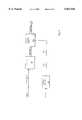
- FIG. 1is a block diagram of a memory system controller chip connected to a an input/output device and an EPROM memory device through a system bus, configured in accordance with a preferred embodiment of the invention.
- FIG. 2is a block diagram of the EPROM of FIG. 1.
- FIG. 3is a block diagram of a plus-one counter of FIG. 2.
- FIG. 4is a block diagram of an alternative apparatus for generating aligned sequential memory addresses.
- FIG. 1illustrates a computer system 10 having a memory system controller 12, an EPROM 14, and an interconnection bus 16. An input/output device 18 is also connected to the interconnection bus 16.
- EPROM 14includes an even array 20 and an odd array 22 for respectively storing read-only data having even and odd memory addresses.
- EPROM 14also includes a burst mode interleaving controller 24 which receives an initial burst mode address along bus 16 from memory system controller 12 and retrieves data from arrays 20 and 22 corresponding to all address within a burst address space containing the initial address.
- EPROM 14operates to retrieve all memory locations within a burst address space in response to a single address received along bus line 16.
- FIG. 2illustrates an exemplary embodiment of EPROM 14 in greater detail.
- Primary components of EPROM 14include a burst controller 26, a counter 30, a plus-one counter 32, a plane multiplexer 38 and an output switch 40, in addition to the previously described even and odd memory arrays 20 and 22, respectively.
- Counter controller 41which may be separate from EPROM 14, allows for selection of a particular burst sequencing mode as well as selection of a burst address space size. Operation of counter controller 41 will be described in further detail below.
- each addresswhich identifies a memory location of a single word within a burst address space, includes address bits denoted A0-AN.
- Address bits denoted A1-ANidentify a memory location in both the odd and even EPROM arrays.
- the address bit denoted A0determines the evenness or oddness of the address and is used to identify the array containing data corresponding to the address A0-A1.
- the initial addressis received and processed by a burst controller 26 which also receives a clock signal along line 28.
- the clock signalis generated by conventional means, not shown.
- Burst controller 26outputs address bits A1-AN to counter 30 along a bus line 17 and to plus-one counter 32 also along line 17.
- Burst controller 26also outputs a clock signal "ClockC” to counter 30 along a line 28a and outputs a clock signal "ClockP" to plus-one counter 32 along a second line 28b.
- ClockCis synchronized with the input clock signal but has a frequency of one-half that of the input clock signal.
- ClockPalso has a frequency one-half that of the input clock signal but is out-of-phase from signal ClockC.
- Burst controller 26also outputs bit A0 to plus2 one counter 32 and to plane multiplexer 38 along line 18a. Burst controller 26 also outputs a modified bit BA0 to output switch 40 along a line 18b. Bit BA0 is generated by receiving initial bit A0 and incrementing bit A0 by one on each clock cycle of the input clock signal. In this manner, BA0 alternates between 1 and 0. As will be described more fully below, address bit A0 and modified bit BA0 are used to facilitate generation of all addresses within the burst address space containing the initial address received along bus line 16.
- a "mode control" signalis also received by burst mode interleaving controller 24 which indicates the type of burst mode, i.e. "aligned sequential", "linear sequential", etc. The mode control signal is received along line 37, from a counter control unit 41.
- Counter 30receives N address bits denoted A1-AN of the initial address received along bus line 16. Counter 30 outputs sequentially generated addresses AC1-ACN beginning at the initial address, with each sequential address being incremented by two. More specifically, counter 30 increments A1-AN by a binary one which effectively increments A0-AN by two. For example, if the initial address is even, counter 30 increments address A1-AN to generate a sequence of even addresses, beginning with A1-AN.
- the output of counter 30, AC1-ACNis transmitted to plane multiplexer 38 which routes AC1-ACN to either even array 20 or odd array 22 depending upon whether AC1-ACN corresponds to an even or an odd address.
- a determination of whether AC1-ACN is even or oddis made based on the A0 bit received along line 18a directly from burst controller 26. If bit A0 is one, then all data output from counter 30 is odd. Hence partial address AC1-ACN is routed to odd array 22. In FIG. 2, the data routed between plane multiplexer 38 and odd array 22 is identified by partial address A01-A0N. If bit A0 is zero, then all addresses output from counter 30 are even. Hence, partial address AC1-ACN is routed to even array 20. In FIG. 2, all addresses routed from plane multiplexer 38 to even array 20 are identified by AE1-AEN.
- counter 30merely provides a partial address AC1-ACN, which does not, by itself, provide any indication whether it corresponds to an even address or an odd address.
- Plane multiplexer 38relies on the state of the A0 bit of the initial address received along bus line 16 to determine whether partial address AC1-ACN corresponds to an even or an odd address.
- all partial addresses AC1-ACN output from counter 30are also even, and are thereby routed to even array 20.
- initial address A0-ANis odd
- all partial addresses output from counter 30are odd and are routed to odd array 22.
- the converseis true for partial addresses AP1-APN output from plus-one counter 32.
- the state of the A0 bit of the initial addressdoes not change during the accessing of all addresses within the burst space. However, when a next "initial" address is received corresponding to a next burst space, the evenness and oddness of partial addresses provided by counter 30 and plus-one counter 32 may change.
- the partial addresses AE1-AEN and AO1-AON sent to the even and odd arrays respectively,are used by the arrays to access data stored therein.
- An A0 bitis not required for input to either the even or odd arrays since the arrays contain either only even or only odd data.
- a partial N-bit addressis sufficient to uniquely identify each memory location within the even or odd arrays.
- Datais output from even array 20 and from odd array 22 asynchronously.
- Output switch 40passes data alternately from even array 20 and odd array 22 for output, with new data effectively output at each rising edge of the input clock signal (received along clock line 28) which controls BA0 that is connected to output switch 40.
- Plus-one counter 32receives bits A1-AN of the initial address along with bit A0. Plus-one counter 32 outputs sequentially generated addresses with each sequential address being incremented by two. As with the operation of counter 30, plus-one counter 32 achieves the incrementing of the overall address A0-AN by 2 by adding a binary 1 to the partial address, A1-AN. Unlike counter 30, plus-one counter 32 initially increments the overall address, A0-AN, by 1.
- the A0 bitis forced into a low state prior to the initial increment by one, in other words, the A0 bit is set to zero before input to plus-one counter 32.
- All subsequent incrementing by twois applied solely to the partial memory address A1-AN resulting from truncating the A0 bit after an initial increment by one. For example, if the initial address is even and for a linear burst sequencing mode, plus-one counter 32 initially adds one to A0-AN to generate a modified full address. Then, counter 32 generates a sequence of addresses based only on A1-AN of the modified address. (For certain sequencing mode, described below, no initial increment by 1 is required.) The operation of counter 32 is synchronized to clock signal "ClockP" received along line 28b. The operation of plus-one counter 32 will be described in further detail below with reference to FIG. 3.
- counter 30operates to generate a sequence of odd address
- plus-one counter 32operates to generate a sequence of even addresses.
- Addresses output by counter 30are routed through plane multiplexer 38 which selects the proper even or odd array, depending upon whether the initial address is even or odd as determined by the state of the A0 bit received along line 18a. Addresses output by plus-one counter 32 are also processed by plane multiplexer 38 and routed to the appropriate memory array.
- Data retrieved by both the even and odd arraysare routed through output switch 40 onto output bus line 16 for transmission to memory system controller 12.
- Datais output from output switch 40 at each rising edge of both the ClockC and ClockP signals.
- datais output from output switch 40 at the rate of the clock signal received along the input line 28 with data alternatingly being provided either by even array 20 or odd array 22.
- bits A1-AN of the initial addressare loaded into counter 30 and output through plane multiplexer 38 into even array 20. Data accessed at that even address location is output from even array 20 through output switch 40. Hence data corresponding to the initial address is the first data to be output from output switch 40. All bits A0-AN are also applied to plus-one counter 32 which increments the overall address by 1 to generate an odd address corresponding to the first burst. Bits AP1l-APN of the odd address are directed through plane multiplexer 38 to odd array 22 and data is subsequently set-up to the output switch.
- BA0increments causing odd data to pass through the output switch and the rising edge of clockC causes counter 30 to increment AC1-ACN. BA0 increments again which causes even array data to pass through the output switch.
- the rising edge of clockPcauses counter 32 to increment AP1-APN and output the address through multiplexer 38 into odd array 22. This sequence repeats until all addresses within the burst address space are accessed.
- Counter 30increments the initial address by two to generate a second even address.
- the second even addressis routed through multiplexer 38 to even array 20. Data retrieved from even array 20 at the second even address is then output through output switch 40. Plus one counter 32 increments the first odd address by two to generate a second odd address for routing to odd array 22. Counter 30 increments the second even address by two and so on.
- the use of out-of-phase clock signals ClockC and ClockPallow counters 30 and 32 to operate out-of-phase.
- the counters, multiplexer, arrays and output switchoperate in sequence such that while a counter is outputting an incremented address, the multiplexer, arrays and output switch are operating on previously generated addresses within the same burst address space.
- output switch 40operates to combine the partial addresses AE1-AEN or AO1-AON received from the even or odd arrays, respectively, with alternating bit BA0.
- Bit BA0switches from 1 to 0 on each rising edge of the input clock signal.
- the value of BA0is timed such that when combined by output switch 40 with the partial addresses, the resulting full address is properly either even or odd.
- partial addresses received through even array 20are combined with bit BA0 when BA0 is set to 0.
- Partial addresses received from odd array 22are combined with bit BA0 when bit BA0 is set to 1.
- counter 30 and plus one counter 32output incremented partial addresses which are routed through plane multiplexer 38 to the appropriate even or odd arrays where data is fetched and output through output switch 40. Processing continues until all addresses within the burst address space defined by the initial address have been retrieved. As will be described more fully below, counter 30 and plus one counter 32 include wrap-around means for detecting a burst space boundary. Thus, for example, the system will access all data with in the burst space beginning at the initial address and continuing up to a burst space boundary, then wrap around to retrieve data from the lower addresses within the burst space. In this manner, all addresses within the burst space are accessed prior to receiving a second "initial" address.
- Plus-one counter 32receives address bits A0-AN from burst controller 26.
- Plus-one counter 32includes three main components a mode controller 34, a plus-one adder 33 and a counter 31.
- Partial address A1-ANis input directly to plus-one adder 33.
- Bit A0is routed through mode controller 34 which, depending upon the value of a mode selection signal received along line 37, outputs an unmodified bit A0 or an A0 bit forced to zero.
- the bit output from mode controller 34is identified by AF0.
- plus-one adder 33receives a full address A0-AN, with the A0 bit possibly being reset to zero from its initial value.
- Plus-one adder 33adds one to the full address received then outputs a partial address AA1-AAN to counter 31. Because plus-one adder 33 receives a full address including A0, the addition of one to the full address serves to increment the full address by one. Counter 31 also increments the address it receives by one. However, counter 31 receives only a partial address AA1-AAN. Hence, by incrementing AA1-AAN by one, counter 31 effectively increments the overall address by two. Counter 31 outputs a partial address AP1-APN to plane multiplexer 38 (FIG. 2).
- plus-one adder 33need not add one to the full address AF0:A1-AN, as such is not necessary. Rather, adder 33 need only pass bits A1-AN to counter 31 without any addition or modification.
- plus-one counter 32can be implemented without a separate mode controller.
- plus-one adder 33receives bit A0 and the mode selection signal directly. If the mode selection signal indicates a sequencing mode where A0 is to be set to 0, such as aligned sequential, plus-one adder 33 merely passes A1-AN to counter 31 unmodified as bits AA1-AAN. If the mode selection signal indicates that a mode wherein A0 is not forced to 0, such as a linear sequential mode, then plus-one adder 33 combines A0 with A1-AN, adds one, and then transmits bits AA1-AAN to counter 31.
- the handling of the A0 bit by plus-one counter 32, in conjunction with counter 30 and output switch 40effectively generates an aligned sequential address sequence without requiring the exclusive OR-gates described above in the Description of Related Art.
- the correct evenness or oddness of partial addresses output from counter 30 and plus-one counter 32is maintained by applying the unmodified A0 bit of the initial address directly to plane multiplexer 38 (FIG. 2).
- plane multiplexer 38FIG. 2
- the full address from the datais reconstructed by combining the alternating BA0 bit provided along line 18b with the partial addresses AE1-AEN or AO1-AON.
- the corresponding odd addressis reconstructed by combining AO1-AON with the BA0 bit which is set to one.
- the corresponding full addressis reconstructed by combining the partial AE1-AEN address with bit BA0 when bit BA0 is set to zero.
- Tables II, III, and IVprovide three examples of aligned sequential burst address sequences with a burst space size of 4 words.
- Each tablecontrasts a linear sequential burst with an aligned sequential burst, resulting from forcing A0 low during the aligned sequential address generation then recombining the addresses with bit BA0.
- Table IIcontrasts a linear burst with an aligned sequential burst, with both generated from an input address having bits A1-A0 equal to "11".
- the initial address and every second address thereafteris routed through counter 30, with counter 30 receiving and outputting partial addresses which exclude the lowest ordered bit A0 which, in this example, is only the A1 bit.
- the full addressis reconstructed by combining the BA0 from burst control 26 bit with the partial address received from counter 30.
- counter 30processes the initial address and all remaining odd addresses within the burst space not generated by plus-one counter 32.
- plus-one counter 32generates all other addresses in the burst space.
- plus-one counter 32generates the next even address and all remaining even addresses within the burst space.
- a left half of table IIillustrates the A1 and A0 bits output by output switch 40 in response to an input address of "11" for a linear burst mode.
- a linear sequence of bitsis provided, having a sequence of 3,0,1,2.
- a right half of table IIillustrates a corresponding aligned sequential sequence also beginning with an initial address of "11". As can be seen, an aligned sequence of 3,2,1,0 is provided.
- Tables III and IVprovide corresponding linear and aligned sequences for a initial address of "01" and for an initial address of "00".
- Table IIthe binary values set forth in tables III and IV represent the full addresses after recombination of intermediate partial addresses output from counters 30 and 32 with binary bit BA0.
- the technique of employing a counter to generate a sequence of partial addresses which exclude the A0 bit, followed by recombining the partial addresses with a alternating BA0 bitcan be employed in a variety of applications, in addition to the interleaved memory architecture set forth in FIGS. 1, 2 and 3.
- separate counterssuch as counter 30 and plus-one counter 32 of FIG. 2, are not required. Rather, a single counter may be employed.
- FIG. 4illustrates an apparatus for generating an aligned sequential address which employs only a single counter 100 in combination with an address combiner 102 and a binary incrementer 104.
- Counter 100receives a partial address of A1-AN which is internally converted to a full address, A0-AN with the A0 bit set to zero.
- Counter 100increments the full address by one.
- counter 100 of FIG. 4increments a full address by one.
- the counters of FIGS. 2 and 3generate either only odd or even addresses
- counter 100 of FIG. 4generates both even and odd addresses.
- counter 100internally employs a full address, including an A0 bit which is initially set to zero, counter 100 outputs only N bits, represented by AP1-APN.
- Binary incrementer 104receives bit A0 of the initial address and increments bit A0 by on each clock cycle to generate an alternating bit which alternates between 1 and 0 on each clock cycle.
- the alternating bit, denoted BA0is transmitted to address combiner 102 along a line 103.
- Address combiner 102combines partial address AP1-APN with bit BA0 to generate a full output address, represented in FIG. 4 by a AMO-AMN.
- the architecture illustrated in FIG. 4may be used in connection with a non-interleaved memory array wherein separate generation of even and odd addresses is not necessary.
- the advantages of generating an aligned sequential address sequence without requiring the additional gate delays described abovecan be gained in a variety of memory architectures and generally in any application requiring the generation of aligned sequential addresses.
- FIG. 4is configured for generating only aligned sequential addresses, and does not include a capability to alternatively generate other sequence modes.
- Counter 30 and counter 31both each include wrap-around circuitry that causes the respective counter to reset when the burst address space boundary is ready to be crossed.
- Information regarding the burst address spaceincluding the burst address space size, is transmitted to each counter along line 35 from counter controller 41. If a next incremental address is not within the original burst address space, the wrap-around circuitry resets the counter to a lowest address which is within the burst address space, e.g. "0000".
- the upper burst space boundaryis defined by an address having all ones, e.g.
- counters 30 and 33do not operate on the lowest ordered bit, hence the comparison between the addresses generated by the counters and the upper address boundary is based on only bits A1-AN.) Thereafter, counter 30 and counter 31 incrementally generate all remaining addresses within the burst address space up to the initial address. In this manner, all addresses within a particular burst address space are fetched from the even and odd EPROM arrays before addresses from a second burst space are fetched (corresponding to a second "initial" address received from memory system controller 12 of FIG. 1). As can be appreciated, because all addresses within a burst space are accessed with individual addresses alternatingly fetched from the even and odd array, output of the entire burst address space occurs at high speed.
- the wrap control circuitry provided within each countercan consist of a "lookahead" circuit that compares the output of each stage of the counter (i.e., each bit in the binary address being incremented) and resets the counter when all bits are set to "1". Since the counters advance the address A1-AN by one (or, equivalent, A0-AN by two), the counters effectively do not make use of A0 when advancing the address.
- counter controller 41provides signals indicating the burst address space size to the counters along line 35 for use in determining when wrap-around should occur.
- the burst address space size signalsmay alternatively be received through bus 16 (FIG. 1) or through other conventional means.
- the burst address space sizeis programmer selectable.
- Counter controller 41also provides the mode selection signal to the mode controller of plus-one counter 32 along line 37. Any circuitry required to implement counter controller 41 is provided in accordance with conventional hardware or software techniques.
- input/output device 18(FIG. 1) may be employed for allowing a user to input a burst sequencing mode and a first address space size, possibly within the parameters of the computer program for controlling operation of EPROM 14.
- any signals needed to implement the selectable burst size or address sequencing modemay be routed through, or generated by, memory system controller 12 (FIG. 1).
- the EPROM chip of the inventioncan be configured to allow a manufacturer to set these parameters, perhaps by employing additional EPROM memory cells, prior to shipment to end users.
- the selectability of the burst address space and the sequencing modeis not limited solely to the end user but such selections may, for particular applications, be reserved to the manufacturer or vendor.
- Other methods for selecting burst address size or burst address sequencing modemay employ any memory element, a fuse element, or even a change in one or more processing steps that hooks up counter control or counters differently.
- the inventionprovides for high-speed access to data stored in EPROM memory arrays (or other similar memory devices). By accessing addresses in a burst address sequence using interleaved memory arrays, high-speed access is assured, i.e., high-speed access is deterministic rather than merely statistical or probabilistic.
- an EPROM memory chipconfigured in accordance with the principles of the invention, is ideally suited for many applications requiring high-speed access to read-only memory.
- the EPROM chips of the inventionare preferably designed and configured using conventional VLSI design and fabrication techniques.
Landscapes
- Engineering & Computer Science (AREA)
- Microelectronics & Electronic Packaging (AREA)
- Dram (AREA)
Abstract
Description
TABLE I ______________________________________ External Internal Address Counter Address ______________________________________ Initial 11 ⊕ 00 = 11 3 Address 1st Burst 11 ⊕ 01 = 10 2 2nd Burst 11 ⊕ 10 = 01 1 3rd Burst 11 ⊕ 11 = 00 0 ______________________________________
TABLE II ______________________________________ Linear Sequential Aligned Burst Sequential Burst ______________________________________ Initial Address 11 3 11 3 1st Burst 00 0 10 2 2nd Burst 01 1 01 13rd Burst 10 2 00 0 ______________________________________
TABLE III ______________________________________ Linear Sequential Aligned Burst Sequential Burst ______________________________________ Initial Address 01 1 01 11st Burst 10 2 00 0 2nd Burst 11 3 11 3 3rd Burst 00 0 10 2 ______________________________________
TABLE IV ______________________________________ Linear Sequential Aligned Burst Sequential Burst ______________________________________ Initial Address 00 0 00 0 1st Burst 01 1 01 12nd Burst 10 2 10 2 3rd Burst 11 3 11 3 ______________________________________
Claims (20)
Priority Applications (2)
| Application Number | Priority Date | Filing Date | Title |
|---|---|---|---|
| US08/473,076US5831926A (en) | 1993-09-17 | 1995-06-07 | Memory architecture for burst mode access |
| US08/745,876US5787047A (en) | 1993-09-17 | 1996-11-08 | Memory architecture for burst mode access |
Applications Claiming Priority (2)
| Application Number | Priority Date | Filing Date | Title |
|---|---|---|---|
| US08/123,377US5453957A (en) | 1993-09-17 | 1993-09-17 | Memory architecture for burst mode access |
| US08/473,076US5831926A (en) | 1993-09-17 | 1995-06-07 | Memory architecture for burst mode access |
Related Parent Applications (1)
| Application Number | Title | Priority Date | Filing Date |
|---|---|---|---|
| US08/123,377DivisionUS5453957A (en) | 1993-09-17 | 1993-09-17 | Memory architecture for burst mode access |
Related Child Applications (1)
| Application Number | Title | Priority Date | Filing Date |
|---|---|---|---|
| US08/745,876DivisionUS5787047A (en) | 1993-09-17 | 1996-11-08 | Memory architecture for burst mode access |
Publications (1)
| Publication Number | Publication Date |
|---|---|
| US5831926Atrue US5831926A (en) | 1998-11-03 |
Family
ID=22408337
Family Applications (3)
| Application Number | Title | Priority Date | Filing Date |
|---|---|---|---|
| US08/123,377Expired - Fee RelatedUS5453957A (en) | 1993-09-17 | 1993-09-17 | Memory architecture for burst mode access |
| US08/473,076Expired - LifetimeUS5831926A (en) | 1993-09-17 | 1995-06-07 | Memory architecture for burst mode access |
| US08/745,876Expired - LifetimeUS5787047A (en) | 1993-09-17 | 1996-11-08 | Memory architecture for burst mode access |
Family Applications Before (1)
| Application Number | Title | Priority Date | Filing Date |
|---|---|---|---|
| US08/123,377Expired - Fee RelatedUS5453957A (en) | 1993-09-17 | 1993-09-17 | Memory architecture for burst mode access |
Family Applications After (1)
| Application Number | Title | Priority Date | Filing Date |
|---|---|---|---|
| US08/745,876Expired - LifetimeUS5787047A (en) | 1993-09-17 | 1996-11-08 | Memory architecture for burst mode access |
Country Status (1)
| Country | Link |
|---|---|
| US (3) | US5453957A (en) |
Cited By (28)
| Publication number | Priority date | Publication date | Assignee | Title |
|---|---|---|---|---|
| US5943292A (en)* | 1997-03-06 | 1999-08-24 | Kabushiki Kaisha Toshiba | Address counter circuit and semiconductor memory device |
| US6081853A (en)* | 1998-03-03 | 2000-06-27 | Ip First, Llc | Method for transferring burst data in a microprocessor |
| US6215729B1 (en) | 2000-06-30 | 2001-04-10 | Micron Technology, Inc. | Programmable counter circuit for generating a sequential/interleave address sequence |
| US6363032B2 (en) | 2000-06-30 | 2002-03-26 | Micron Technology, Inc. | Programmable counter circuit for generating a sequential/interleave address sequence |
| US20020109698A1 (en)* | 2001-02-15 | 2002-08-15 | Mark Champion | Checkerboard buffer using memory blocks |
| US20020109693A1 (en)* | 2001-02-15 | 2002-08-15 | Mark Champion | Checkerboard buffer using two-dimensional buffer pages |
| US20020109694A1 (en)* | 2001-02-15 | 2002-08-15 | Mark Champion | Checkerboard buffer using two-dimensional buffer pages and using bit-field addressing |
| US20020110030A1 (en)* | 2001-02-15 | 2002-08-15 | Mark Champion | Swapped Pixel pages |
| US20020109792A1 (en)* | 2001-02-15 | 2002-08-15 | Mark Champion | Two-dimensional buffer pages using memory bank alternation |
| US20020109690A1 (en)* | 2001-02-15 | 2002-08-15 | Mark Champion | Checkerboard buffer using memory bank alternation |
| US20020110351A1 (en)* | 2001-02-15 | 2002-08-15 | Mark Champion | Checkerboard buffer |
| US20020109689A1 (en)* | 2001-02-15 | 2002-08-15 | Mark Champion | Checkerboard buffer using sequential memory locations |
| US20020109691A1 (en)* | 2001-02-15 | 2002-08-15 | Mark Champion | Two-dimensional buffer pages using state addressing |
| US20020109791A1 (en)* | 2001-02-15 | 2002-08-15 | Mark Champion | Two-dimensional buffer pages |
| US20020109696A1 (en)* | 2001-02-15 | 2002-08-15 | Mark Champion | Checkerboard buffer using two-dimensional buffer pages and using memory bank alternation |
| US20020109695A1 (en)* | 2001-02-15 | 2002-08-15 | Mark Champion | Checkerboard buffer using two-dimensional buffer pages and using state addressing |
| US20020109692A1 (en)* | 2001-02-15 | 2002-08-15 | Sony Corporation | Dynamic buffer pages |
| US20020113904A1 (en)* | 2001-02-15 | 2002-08-22 | Mark Champion | Two-dimensional buffer pages using bit-field addressing |
| US20030058368A1 (en)* | 2001-09-24 | 2003-03-27 | Mark Champion | Image warping using pixel pages |
| US6564285B1 (en)* | 1994-06-03 | 2003-05-13 | Intel Corporation | Synchronous interface for a nonvolatile memory |
| US20030151609A1 (en)* | 2002-02-14 | 2003-08-14 | Mark Champion | Multi-sequence burst accessing for SDRAM |
| US6629223B2 (en)* | 1998-10-06 | 2003-09-30 | Texas Instruments Incorporated | Method and apparatus for accessing a memory core multiple times in a single clock cycle |
| US6708264B1 (en)* | 1999-06-15 | 2004-03-16 | Kabushiki Kaisha Toshiba | Synchronous memory device with prefetch address counter |
| WO2004047112A1 (en)* | 2002-11-20 | 2004-06-03 | Koninklijke Philips Electronics N.V. | Sdram address mapping optimized for two-dimensional access |
| US20040233206A1 (en)* | 2001-02-15 | 2004-11-25 | Sony Corporation, A Japanese Corporation | Pixel pages optimized for GLV |
| US20060149878A1 (en)* | 2004-12-30 | 2006-07-06 | Carmichael Richard D | Efficient interrupt processing in systems with multiple serial protocol engines |
| US20080235438A1 (en)* | 2007-03-20 | 2008-09-25 | Sony Corporation And Sony Electronics Inc. | System and method for effectively implementing a multiple-channel memory architecture |
| US20100287343A1 (en)* | 2008-01-21 | 2010-11-11 | Freescale Semiconductor, Inc. | Contention free parallel access system and a method for contention free parallel access to a group of memory banks |
Families Citing this family (33)
| Publication number | Priority date | Publication date | Assignee | Title |
|---|---|---|---|---|
| US5453957A (en)* | 1993-09-17 | 1995-09-26 | Cypress Semiconductor Corp. | Memory architecture for burst mode access |
| US5729709A (en)* | 1993-11-12 | 1998-03-17 | Intel Corporation | Memory controller with burst addressing circuit |
| JP3153078B2 (en)* | 1994-09-09 | 2001-04-03 | 日本電気株式会社 | Data processing device |
| US5636361A (en)* | 1994-12-22 | 1997-06-03 | International Business Machines Corporation | Multi-processor computer system having dual memory subsytems for enabling concurrent memory access thereto by more than one processor |
| US5689731A (en)* | 1995-06-07 | 1997-11-18 | International Business Machines Corporation | Programmable serializer using multiplexer and programmable address counter for providing flexiblity in scanning sequences and width of data |
| US5835970A (en)* | 1995-12-21 | 1998-11-10 | Cypress Semiconductor Corp. | Burst address generator having two modes of operation employing a linear/nonlinear counter using decoded addresses |
| KR0161868B1 (en)* | 1995-12-27 | 1999-01-15 | 문정환 | Memory address control circuit |
| US5715476A (en)* | 1995-12-29 | 1998-02-03 | Intel Corporation | Method and apparatus for controlling linear and toggle mode burst access sequences using toggle mode increment logic |
| JPH09231764A (en)* | 1996-01-19 | 1997-09-05 | Sgs Thomson Microelectron Inc | Burst counter circuit and operating method therefor |
| US5783958A (en)* | 1996-01-19 | 1998-07-21 | Sgs-Thomson Microelectronics, Inc. | Switching master slave circuit |
| JPH10162568A (en)* | 1996-12-02 | 1998-06-19 | Toshiba Corp | Semiconductor storage device |
| US5784331A (en)* | 1996-12-31 | 1998-07-21 | Sgs-Thomson Microelectronics, Inc. | Multiple access memory device |
| KR100229897B1 (en)* | 1997-01-10 | 1999-11-15 | 윤종용 | Timing Mode Selection Device According to Direct Memory Access Transmission Method |
| JP3907785B2 (en)* | 1997-06-04 | 2007-04-18 | 富士通株式会社 | Semiconductor memory device |
| US6138214A (en)* | 1997-12-19 | 2000-10-24 | Siemens Aktiengesellschaft | Synchronous dynamic random access memory architecture for sequential burst mode |
| JP3075352B2 (en)* | 1998-04-15 | 2000-08-14 | 日本電気株式会社 | Method and apparatus for supplying chemical mechanical polishing liquid |
| US6128244A (en)* | 1998-06-04 | 2000-10-03 | Micron Technology, Inc. | Method and apparatus for accessing one of a plurality of memory units within an electronic memory device |
| US6480510B1 (en) | 1998-07-28 | 2002-11-12 | Serconet Ltd. | Local area network of serial intelligent cells |
| JP2000285016A (en)* | 1999-03-30 | 2000-10-13 | Sanyo Electric Co Ltd | Memory control circuit |
| DE19944040C2 (en)* | 1999-09-14 | 2001-11-22 | Infineon Technologies Ag | Integrated memory with two burst modes |
| US6452864B1 (en)* | 2000-01-31 | 2002-09-17 | Stmicroelectonics S.R.L. | Interleaved memory device for sequential access synchronous reading with simplified address counters |
| US6785764B1 (en)* | 2000-05-11 | 2004-08-31 | Micron Technology, Inc. | Synchronous flash memory with non-volatile mode register |
| EP1195770B1 (en)* | 2000-10-06 | 2009-05-27 | STMicroelectronics S.r.l. | Internal addressing structure of a semiconductor memory |
| EP1220225A1 (en)* | 2000-12-28 | 2002-07-03 | STMicroelectronics S.r.l. | Method and device for reducing the mean access time to a non volatile memory during the reading phase |
| US7383321B2 (en) | 2002-07-09 | 2008-06-03 | Moyer Alan L | Method and system for communicating between a remote printer and a server |
| TW559809B (en)* | 2002-03-27 | 2003-11-01 | Via Tech Inc | Memory control chip, control method and control circuit |
| US7003684B2 (en)* | 2002-03-27 | 2006-02-21 | Via Technologies, Inc. | Memory control chip, control method and control circuit |
| KR100437467B1 (en)* | 2002-07-03 | 2004-06-23 | 삼성전자주식회사 | Multi-chip system having continuous burst read mode of operation |
| CA2479868A1 (en)* | 2003-09-02 | 2005-03-02 | Ronald E. Brick | Light fixture |
| CN100433195C (en)* | 2003-12-31 | 2008-11-12 | 深圳市朗科科技股份有限公司 | Flash memory medium data writing method |
| US7634622B1 (en) | 2005-06-14 | 2009-12-15 | Consentry Networks, Inc. | Packet processor that generates packet-start offsets to immediately store incoming streamed packets using parallel, staggered round-robin arbitration to interleaved banks of memory |
| US7436708B2 (en)* | 2006-03-01 | 2008-10-14 | Micron Technology, Inc. | NAND memory device column charging |
| US8427874B2 (en) | 2010-04-30 | 2013-04-23 | SanDisk Technologies, Inc. | Non-volatile memory and method with even/odd combined block decoding |
Citations (9)
| Publication number | Priority date | Publication date | Assignee | Title |
|---|---|---|---|---|
| US4247920A (en)* | 1979-04-24 | 1981-01-27 | Tektronix, Inc. | Memory access system |
| US4847809A (en)* | 1985-07-10 | 1989-07-11 | Kabushiki Kaisha Toshiba | Image memory having standard dynamic RAM chips |
| US4849937A (en)* | 1984-12-14 | 1989-07-18 | Mitsubishi Denki Kabushiki Kaisha | Digital delay unit with interleaved memory |
| US4903217A (en)* | 1987-02-12 | 1990-02-20 | International Business Machines Corp. | Frame buffer architecture capable of accessing a pixel aligned M by N array of pixels on the screen of an attached monitor |
| US4924375A (en)* | 1987-10-23 | 1990-05-08 | Chips And Technologies, Inc. | Page interleaved memory access |
| US4991110A (en)* | 1988-09-13 | 1991-02-05 | Silicon Graphics, Inc. | Graphics processor with staggered memory timing |
| US5121354A (en)* | 1990-03-12 | 1992-06-09 | International Business Machines Corp. | Random access memory with access on bit boundaries |
| US5453957A (en)* | 1993-09-17 | 1995-09-26 | Cypress Semiconductor Corp. | Memory architecture for burst mode access |
| US5469558A (en)* | 1991-08-16 | 1995-11-21 | Multichip Technology | Dynamically reconfigurable memory system with programmable controller and FIFO buffered data channels |
- 1993
- 1993-09-17USUS08/123,377patent/US5453957A/ennot_activeExpired - Fee Related
- 1995
- 1995-06-07USUS08/473,076patent/US5831926A/ennot_activeExpired - Lifetime
- 1996
- 1996-11-08USUS08/745,876patent/US5787047A/ennot_activeExpired - Lifetime
Patent Citations (9)
| Publication number | Priority date | Publication date | Assignee | Title |
|---|---|---|---|---|
| US4247920A (en)* | 1979-04-24 | 1981-01-27 | Tektronix, Inc. | Memory access system |
| US4849937A (en)* | 1984-12-14 | 1989-07-18 | Mitsubishi Denki Kabushiki Kaisha | Digital delay unit with interleaved memory |
| US4847809A (en)* | 1985-07-10 | 1989-07-11 | Kabushiki Kaisha Toshiba | Image memory having standard dynamic RAM chips |
| US4903217A (en)* | 1987-02-12 | 1990-02-20 | International Business Machines Corp. | Frame buffer architecture capable of accessing a pixel aligned M by N array of pixels on the screen of an attached monitor |
| US4924375A (en)* | 1987-10-23 | 1990-05-08 | Chips And Technologies, Inc. | Page interleaved memory access |
| US4991110A (en)* | 1988-09-13 | 1991-02-05 | Silicon Graphics, Inc. | Graphics processor with staggered memory timing |
| US5121354A (en)* | 1990-03-12 | 1992-06-09 | International Business Machines Corp. | Random access memory with access on bit boundaries |
| US5469558A (en)* | 1991-08-16 | 1995-11-21 | Multichip Technology | Dynamically reconfigurable memory system with programmable controller and FIFO buffered data channels |
| US5453957A (en)* | 1993-09-17 | 1995-09-26 | Cypress Semiconductor Corp. | Memory architecture for burst mode access |
Cited By (57)
| Publication number | Priority date | Publication date | Assignee | Title |
|---|---|---|---|---|
| US6564285B1 (en)* | 1994-06-03 | 2003-05-13 | Intel Corporation | Synchronous interface for a nonvolatile memory |
| US5943292A (en)* | 1997-03-06 | 1999-08-24 | Kabushiki Kaisha Toshiba | Address counter circuit and semiconductor memory device |
| US6081853A (en)* | 1998-03-03 | 2000-06-27 | Ip First, Llc | Method for transferring burst data in a microprocessor |
| US6629223B2 (en)* | 1998-10-06 | 2003-09-30 | Texas Instruments Incorporated | Method and apparatus for accessing a memory core multiple times in a single clock cycle |
| US20040109381A1 (en)* | 1998-10-06 | 2004-06-10 | Jean-Marc Bachot | Method and apparatus for accessing a memory core multiple times in a single clock cycle |
| US7035985B2 (en)* | 1998-10-06 | 2006-04-25 | Texas Instruments Incorporated | Method and apparatus for accessing a memory core multiple times in a single clock cycle |
| US6708264B1 (en)* | 1999-06-15 | 2004-03-16 | Kabushiki Kaisha Toshiba | Synchronous memory device with prefetch address counter |
| US6215729B1 (en) | 2000-06-30 | 2001-04-10 | Micron Technology, Inc. | Programmable counter circuit for generating a sequential/interleave address sequence |
| US6363032B2 (en) | 2000-06-30 | 2002-03-26 | Micron Technology, Inc. | Programmable counter circuit for generating a sequential/interleave address sequence |
| US20040246258A1 (en)* | 2001-02-15 | 2004-12-09 | Sony Corporation | Swapped pixel pages |
| US6850241B2 (en) | 2001-02-15 | 2005-02-01 | Sony Corporation | Swapped pixel pages |
| US20020110030A1 (en)* | 2001-02-15 | 2002-08-15 | Mark Champion | Swapped Pixel pages |
| US20020109792A1 (en)* | 2001-02-15 | 2002-08-15 | Mark Champion | Two-dimensional buffer pages using memory bank alternation |
| US20020109690A1 (en)* | 2001-02-15 | 2002-08-15 | Mark Champion | Checkerboard buffer using memory bank alternation |
| US20020110351A1 (en)* | 2001-02-15 | 2002-08-15 | Mark Champion | Checkerboard buffer |
| US20020109689A1 (en)* | 2001-02-15 | 2002-08-15 | Mark Champion | Checkerboard buffer using sequential memory locations |
| US20020109691A1 (en)* | 2001-02-15 | 2002-08-15 | Mark Champion | Two-dimensional buffer pages using state addressing |
| US20020109791A1 (en)* | 2001-02-15 | 2002-08-15 | Mark Champion | Two-dimensional buffer pages |
| US20020109696A1 (en)* | 2001-02-15 | 2002-08-15 | Mark Champion | Checkerboard buffer using two-dimensional buffer pages and using memory bank alternation |
| US20020109695A1 (en)* | 2001-02-15 | 2002-08-15 | Mark Champion | Checkerboard buffer using two-dimensional buffer pages and using state addressing |
| US20020109692A1 (en)* | 2001-02-15 | 2002-08-15 | Sony Corporation | Dynamic buffer pages |
| US20020113904A1 (en)* | 2001-02-15 | 2002-08-22 | Mark Champion | Two-dimensional buffer pages using bit-field addressing |
| US6795079B2 (en) | 2001-02-15 | 2004-09-21 | Sony Corporation | Two-dimensional buffer pages |
| US8547384B2 (en) | 2001-02-15 | 2013-10-01 | Sony Corporation | Checkerboard buffer |
| US6801204B2 (en) | 2001-02-15 | 2004-10-05 | Sony Corporation, A Japanese Corporation | Checkerboard buffer using memory blocks |
| US6803917B2 (en) | 2001-02-15 | 2004-10-12 | Sony Corporation | Checkerboard buffer using memory bank alternation |
| US20040233206A1 (en)* | 2001-02-15 | 2004-11-25 | Sony Corporation, A Japanese Corporation | Pixel pages optimized for GLV |
| US6828977B2 (en) | 2001-02-15 | 2004-12-07 | Sony Corporation | Dynamic buffer pages |
| US20020109693A1 (en)* | 2001-02-15 | 2002-08-15 | Mark Champion | Checkerboard buffer using two-dimensional buffer pages |
| US6831650B2 (en) | 2001-02-15 | 2004-12-14 | Sony Corporation | Checkerboard buffer using sequential memory locations |
| US6831649B2 (en) | 2001-02-15 | 2004-12-14 | Sony Corporation | Two-dimensional buffer pages using state addressing |
| US6831651B2 (en) | 2001-02-15 | 2004-12-14 | Sony Corporation | Checkerboard buffer |
| US20020109694A1 (en)* | 2001-02-15 | 2002-08-15 | Mark Champion | Checkerboard buffer using two-dimensional buffer pages and using bit-field addressing |
| US20050024368A1 (en)* | 2001-02-15 | 2005-02-03 | Xiping Liu | Two dimensional buffer pages |
| US20050057572A1 (en)* | 2001-02-15 | 2005-03-17 | Sony Corporation | Checkerboard buffer |
| US20050104890A1 (en)* | 2001-02-15 | 2005-05-19 | Sony Corporation | Dynamic buffer pages |
| US7830391B2 (en) | 2001-02-15 | 2010-11-09 | Sony Corporation | Checkerboard buffer using two-dimensional buffer pages |
| US7573483B2 (en) | 2001-02-15 | 2009-08-11 | Sony Corporation, A Japanese Corporation | Dynamic buffer pages |
| US6992674B2 (en) | 2001-02-15 | 2006-01-31 | Sony Corporation | Checkerboard buffer using two-dimensional buffer pages and using state addressing |
| US7379069B2 (en) | 2001-02-15 | 2008-05-27 | Sony Corporation | Checkerboard buffer using two-dimensional buffer pages |
| US7205993B2 (en) | 2001-02-15 | 2007-04-17 | Sony Corporation | Checkerboard buffer using two-dimensional buffer pages and using memory bank alternation |
| US20020109698A1 (en)* | 2001-02-15 | 2002-08-15 | Mark Champion | Checkerboard buffer using memory blocks |
| US7038691B2 (en) | 2001-02-15 | 2006-05-02 | Sony Corporation | Two-dimensional buffer pages using memory bank alternation |
| US7046249B2 (en) | 2001-02-15 | 2006-05-16 | Sony Corporation | Swapped pixel pages |
| US7068281B2 (en) | 2001-02-15 | 2006-06-27 | Sony Corporation | Pixel pages optimized for GLV |
| US7129953B2 (en) | 2001-02-15 | 2006-10-31 | Sony Corporation | Two dimensional buffer pages |
| US7088369B2 (en) | 2001-02-15 | 2006-08-08 | Sony Corporation | Checkerboard buffer using two-dimensional buffer pages and using bit-field addressing |
| US20030058368A1 (en)* | 2001-09-24 | 2003-03-27 | Mark Champion | Image warping using pixel pages |
| US6965980B2 (en)* | 2002-02-14 | 2005-11-15 | Sony Corporation | Multi-sequence burst accessing for SDRAM |
| US20030151609A1 (en)* | 2002-02-14 | 2003-08-14 | Mark Champion | Multi-sequence burst accessing for SDRAM |
| US20060047890A1 (en)* | 2002-11-20 | 2006-03-02 | Van De Waerdt Jan-Willem | Sdram address mapping optimized for two-dimensional access |
| US7221612B2 (en) | 2002-11-20 | 2007-05-22 | Nxp B.V. | SDRAM address mapping optimized for two-dimensional access |
| WO2004047112A1 (en)* | 2002-11-20 | 2004-06-03 | Koninklijke Philips Electronics N.V. | Sdram address mapping optimized for two-dimensional access |
| US20060149878A1 (en)* | 2004-12-30 | 2006-07-06 | Carmichael Richard D | Efficient interrupt processing in systems with multiple serial protocol engines |
| US20080235438A1 (en)* | 2007-03-20 | 2008-09-25 | Sony Corporation And Sony Electronics Inc. | System and method for effectively implementing a multiple-channel memory architecture |
| US20100287343A1 (en)* | 2008-01-21 | 2010-11-11 | Freescale Semiconductor, Inc. | Contention free parallel access system and a method for contention free parallel access to a group of memory banks |
| US8627022B2 (en)* | 2008-01-21 | 2014-01-07 | Freescale Semiconductor, Inc. | Contention free parallel access system and a method for contention free parallel access to a group of memory banks |
Also Published As
| Publication number | Publication date |
|---|---|
| US5453957A (en) | 1995-09-26 |
| US5787047A (en) | 1998-07-28 |
Similar Documents
| Publication | Publication Date | Title |
|---|---|---|
| US5831926A (en) | Memory architecture for burst mode access | |
| US5386385A (en) | Method and apparatus for preventing invalid operating modes and an application to synchronous memory devices | |
| US5912854A (en) | Data processing system arranged for operating synchronously with a high speed memory | |
| US6636446B2 (en) | Semiconductor memory device having write latency operation and method thereof | |
| US5345573A (en) | High speed burst read address generation with high speed transfer | |
| US4845664A (en) | On-chip bit reordering structure | |
| US6026050A (en) | Method and apparatus for adaptively adjusting the timing of a clock signal used to latch digital signals, and memory device using same | |
| US4323965A (en) | Sequential chip select decode apparatus and method | |
| US4384342A (en) | System for reducing access time to plural memory modules using five present-fetch and one prefetch address registers | |
| US5278967A (en) | System for providing gapless data transfer from page-mode dynamic random access memories | |
| US6128244A (en) | Method and apparatus for accessing one of a plurality of memory units within an electronic memory device | |
| KR20020086542A (en) | Memory device with support for unaligned access | |
| US4432055A (en) | Sequential word aligned addressing apparatus | |
| US5835970A (en) | Burst address generator having two modes of operation employing a linear/nonlinear counter using decoded addresses | |
| US6191997B1 (en) | Memory burst operations in which address count bits are used as column address bits for one, but not both, of the odd and even columns selected in parallel. | |
| EP0829804B1 (en) | Synchronous semiconductor memory device having macro command storage and execution method therefor | |
| US5663924A (en) | Boundary independent bit decode for a SDRAM | |
| US4376972A (en) | Sequential word aligned address apparatus | |
| EP0690450B1 (en) | Memory circuit sequentially accessible by arbitrary address | |
| US6016537A (en) | Method and apparatus for address multiplexing to support variable DRAM sizes | |
| US6714475B2 (en) | Fast accessing of a memory device using decoded address during setup time | |
| US6272065B1 (en) | Address generating and decoding circuit for use in burst-type random access memory device having a double data rate, and an address generating method thereof | |
| US4975882A (en) | User programmable redundant memory | |
| JPH0855495A (en) | Reconstituting circuit and method of synchronous memory device as asynchronous memory device | |
| US5276846A (en) | Fast access memory structure |
Legal Events
| Date | Code | Title | Description |
|---|---|---|---|
| STCF | Information on status: patent grant | Free format text:PATENTED CASE | |
| FPAY | Fee payment | Year of fee payment:4 | |
| REMI | Maintenance fee reminder mailed | ||
| SULP | Surcharge for late payment | ||
| FPAY | Fee payment | Year of fee payment:8 | |
| FEPP | Fee payment procedure | Free format text:PAYOR NUMBER ASSIGNED (ORIGINAL EVENT CODE: ASPN); ENTITY STATUS OF PATENT OWNER: LARGE ENTITY Free format text:PAYER NUMBER DE-ASSIGNED (ORIGINAL EVENT CODE: RMPN); ENTITY STATUS OF PATENT OWNER: LARGE ENTITY | |
| FPAY | Fee payment | Year of fee payment:12 | |
| AS | Assignment | Owner name:CYPRESS SEMICONDUCTOR CORPORATION, CALIFORNIA Free format text:ASSIGNMENT OF ASSIGNORS INTEREST;ASSIGNORS:NORRIS, CHRISTOPHER S.;LACEY, TIMOTHY M.;REEL/FRAME:032946/0500 Effective date:19931104 | |
| AS | Assignment | Owner name:RPX CORPORATION, CALIFORNIA Free format text:ASSIGNMENT OF ASSIGNORS INTEREST;ASSIGNOR:CYPRESS SEMICONDUCTOR CORPORATION;REEL/FRAME:033119/0615 Effective date:20140604 | |
| AS | Assignment | Owner name:JPMORGAN CHASE BANK, N.A., AS COLLATERAL AGENT, IL Free format text:SECURITY AGREEMENT;ASSIGNORS:RPX CORPORATION;RPX CLEARINGHOUSE LLC;REEL/FRAME:038041/0001 Effective date:20160226 | |
| AS | Assignment | Owner name:RPX CORPORATION, CALIFORNIA Free format text:RELEASE (REEL 038041 / FRAME 0001);ASSIGNOR:JPMORGAN CHASE BANK, N.A.;REEL/FRAME:044970/0030 Effective date:20171222 Owner name:RPX CLEARINGHOUSE LLC, CALIFORNIA Free format text:RELEASE (REEL 038041 / FRAME 0001);ASSIGNOR:JPMORGAN CHASE BANK, N.A.;REEL/FRAME:044970/0030 Effective date:20171222 |