US5828288A - Pedestal edge emitter and non-linear current limiters for field emitter displays and other electron source applications - Google Patents
Pedestal edge emitter and non-linear current limiters for field emitter displays and other electron source applicationsDownload PDFInfo
- Publication number
- US5828288A US5828288AUS08/518,745US51874595AUS5828288AUS 5828288 AUS5828288 AUS 5828288AUS 51874595 AUS51874595 AUS 51874595AUS 5828288 AUS5828288 AUS 5828288A
- Authority
- US
- United States
- Prior art keywords
- emitter
- current limiter
- sio
- layer
- substrate
- Prior art date
- Legal status (The legal status is an assumption and is not a legal conclusion. Google has not performed a legal analysis and makes no representation as to the accuracy of the status listed.)
- Expired - Fee Related
Links
Images


Classifications
- H—ELECTRICITY
- H01—ELECTRIC ELEMENTS
- H01J—ELECTRIC DISCHARGE TUBES OR DISCHARGE LAMPS
- H01J1/00—Details of electrodes, of magnetic control means, of screens, or of the mounting or spacing thereof, common to two or more basic types of discharge tubes or lamps
- H01J1/02—Main electrodes
- H01J1/30—Cold cathodes, e.g. field-emissive cathode
- H01J1/304—Field-emissive cathodes
- H01J1/3042—Field-emissive cathodes microengineered, e.g. Spindt-type
- H—ELECTRICITY
- H01—ELECTRIC ELEMENTS
- H01J—ELECTRIC DISCHARGE TUBES OR DISCHARGE LAMPS
- H01J2201/00—Electrodes common to discharge tubes
- H01J2201/30—Cold cathodes
- H01J2201/304—Field emission cathodes
- H01J2201/30403—Field emission cathodes characterised by the emitter shape
- H01J2201/30423—Microengineered edge emitters
- H—ELECTRICITY
- H01—ELECTRIC ELEMENTS
- H01J—ELECTRIC DISCHARGE TUBES OR DISCHARGE LAMPS
- H01J2201/00—Electrodes common to discharge tubes
- H01J2201/30—Cold cathodes
- H01J2201/319—Circuit elements associated with the emitters by direct integration
Definitions
- the present inventionrelates to field emission structures and devices, including field emission-based flat panel displays, as well as to methods of manufacture and use of such structures and devices.
- a microelectronic emission elementor a plurality (array) of such elements, is employed to emit a flux of electrons from one or more field emitters.
- the field emitterwhich often is referred to as a "tip" is specifically shaped to facilitate effective emission of electrons, and may for example be conical-, pyramidal-, or ridge-shaped in surface profile.
- Field emitter structureshave wide potential and actual utility in microelectronics applications, including electron guns, display devices comprising the field emitter structure in combination with photoluminescent material on which the emitted electrons are selectively impinged, and vacuum integrated circuits comprising assemblies of emitter tips coupled with associated control electrodes.
- a field emission tipis characteristically arranged in electrical contact with an emitter conductor and in spaced relationship to an extraction electrode, thereby forming an electron emission gap. With a voltage imposed between the emitter tip and extraction electrode, the field emitter tip discharges a flux of electrons.
- the tip or tip arraymay be formed on a suitable substrate such as silicon or other semiconductor material, and associated electrodes may be formed on and/or in the substrate by well-known planar techniques to yield practical microelectronic devices.
- Horizontal field emittersutilize horizontally arranged emitters and electrodes to generate electron beam emission parallel to the (horizontally aligned) substrate.
- vertical field emittersemploy vertically arranged emitters and electrodes to generate electron beam emission perpendicular to the substrate.
- Examples of horizontal field emittersare disclosed in Lambe U.S. Pat. No. 4,728,851 and Lee et al U.S. Pat. No. 4,827,177.
- the Lambe and Lee et al structuresare formed as a single horizontal layer on a substrate.
- An improved horizontal field emitteris disclosed in Jones et al U.S. Pat. No. 5,144,191.
- the sliced membersmay be processed so that the cathode material protrudes above the insulator casing.
- the exposed cathode material in either embodimentthen is shaped into emitter tips (microtip cathodes).
- U.S. Pat. No. 3,665,241discloses vertical field emission cathode/field ionizer structures in which "needle-like" elements such as conical or pyramidal tips are formed on a (typically conductive or semiconductive) substrate. Above this tip array, a foraminous electrode member, such as a screen or mesh, is arranged with its openings vertically aligned with associated tip elements.
- the needle-like elementscomprise a cylindrical lower pedestal section and an upper conical extremity, wherein the pedestal section has a higher resistivity than either the foraminous electrode or the upper conical extremity, and an insulator may be arranged between the conical tip electrodes and the foraminous electrode member.
- the structures of this patentmay be formed by metal deposition through a foraminous member (which may be left in place as a counter-electrode, or replaced with another foraminous member) to yield a regular array of metal points.
- the vertical column emitter structuremay be fabricated by forming the tips on the face of the substrate, followed by forming trenches in the substrate around the tips to form columns having the tips at their uppermost extremities.
- the vertical column emitter structure of U.S. Pat. No. 5,371,431is described as being fabricatable by forming trenches in the substrate to define columns, followed by forming tips on top of the columns.
- the trenchesmay be filled with a dielectric and a conductor layer may be formed on the dielectric to provide extraction electrodes.
- the present inventiona number of structures are provided which enhance the performance and reliability of field emitter devices, particularly field emitter displays.
- the inventionadditionally provides methods for fabricating the structures.
- primary aspects of the inventioninclude a novel emitter structure, herein termed a pedestal edge emitter; and improved non-linear current limiters useful both in combination with the pedestal edge emitters disclosed herein, as well as with various ones of the vertical field emitters disclosed in the patents and applications hereinabove under the heading "Background of the Invention”.
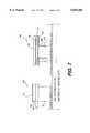
- FIG. 1is a cross-sectional drawing of a flat panel display including one form of pedestal edge emitter in accordance with the invention
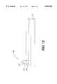
- FIG. 2is a cross-sectional view of another form of pedestal edge emitter in accordance with the invention.
- FIG. 3is a top plan view of a dot-in-circle pedestal edge emitter
- FIG. 4is a top plan view of a portion of a linear pedestal edge emitter
- FIG. 5depicts an intermediate step in a fabrication process
- FIG. 6depicts another step in the process
- FIG. 7depicts a pedestal edge emitter structure wherein dielectric layers are included to control focusing
- FIG. 8depicts a pedestal edge emitter structure including a recessed cap
- FIG. 9depicts a pedestal edge emitter with thin film emitter edges
- FIG. 10depicts a pedestal edge emitter of dish-shaped structure
- FIG. 11depicts a pedestal edge emitter wherein a thin film edge emitter functions as a current limiter
- FIG. 12depicts an alternative current limiter
- FIG. 13depicts gateable current limiter structures.
- a representative environment in which the pedestal edge emitter of the invention may be includedtakes the form of a flat panel display device 50 including an evacuated space 52, and a transparent panel 54 for viewing.
- a transparent panel 54for viewing.
- anode electrode 56On the underside of the panel 54 is a thin transparent anode electrode 56, supporting cathodoluminescent material 58.
- the anode 56is connected to a suitable positive supply voltage, schematically represented at 60.
- a pedestal edge emitter 62in accordance with one embodiment of the invention comprises a conductive column or pedestal 64 supporting an edge emitter electrode in the form of an emitter cap layer 66 having an emitter edge 68.
- the pedestal 64comprises a conductive material, such as Sb and Au-doped silicon.
- Below the cap 68is an optional underlayer 70.
- the conductive pedestal 64is formed on a layer 72 of current limiter material, such as for example arsenic-doped silicon or 50% Cr+50% SiO.
- the layer of current limiter materialmay be either patterned or non-patterned, and is formed over a lower emitter conductor layer 74, likewise either patterned or non-patterned.
- the emitter conductor 74is connected to a supply voltage source represented at 76, which is negative with reference to the anode supply 60.
- the emitter conductor 74is formed over a suitable substrate 78, such as a glass substrate 78.
- a gate electrode 80is fabricated on either side of the edge emitter 62, separated by a gap.
- the gate electrode 80is supported on an insulating stack 82, and is schematically connected to a gate (G) terminal 84.
- the gate terminal (G) 84is appropriately biased to control electron current flow between the edge emitter 62 and the anode 56, and thus producing illumination from the cathodoluminescent layer 58 which can be viewed through transparent electrode 56 and the transparent panel 54.
- either the underlayer 70 or the cap layer 66must be semi-insulating or semiconducting, with the other of the layers 66 and 70 being conducting.
- the purpose of such electrical characteristics of the underlayer and cap layersis to concentrate the electromagnetic field at the emitter edges 68 to achieve the desired controlled emission of electrons.
- an SiO underlayer 70can be constructed under a chromium or diamond-like film cap 66 by evaporating either SiO, or SiO plus a dopant. The SiO deposits on the sidewalls of the pedestal 64, and under the cap 66.
- CVDof a variety of materials, such as GaAs on an undercut chromium cap 66, followed by RIE, can also be used to create a semiconductor or semi-insulating layer.
- An SiO capcan be formed by undercutting a silicon conductive column, and then depositing via CVD a metal such as tungsten (deposited by WF6+SiH4+H2 reduction), followed by employing an SF6+O2 plasma to remove tungsten off the cap surface.
- a metalsuch as tungsten (deposited by WF6+SiH4+H2 reduction)
- FIG. 2depicts a related alternative pedestal edge emitter structure 80 wherein the current limiter material layer 72 of FIG. 1 is eliminated, and a pedestal 84 comprises current limiter material, formed over the cathode conductor layer 74.
- the use of the resistor or current limiter to form the columnar current limiter 84reduces step height at the edges of the emitter conductor 72.
- FIG. 3is a plan view depicting a configuration wherein the pedestal edge emitter structures of FIGS. 1 and 2 comprise a dot-in-circle pattern
- FIG. 4is a plan view depicting a linear pattern. Dot-in-circle patterns are preferred in most display applications.
- the emitter capis formed by deposition of a thin-film emitter material, such as silicon, Nb, diamond-like carbon, Ba/Sr--O, SiO2, SiO+Cr, or SiO2+Cr or Nb.
- a thin-film emitter materialsuch as silicon, Nb, diamond-like carbon, Ba/Sr--O, SiO2, SiO+Cr, or SiO2+Cr or Nb.
- the capis purposely left in place, or thinned, leaving a select layer or layers of edge emitter material, by deposition, etching, formation and material removal techniques conventionally known and employed in the art.
- the emitter conductor layer 74for example Al+Cu, is formed over the glass substrate 78, followed by the resistor or current limiter layer 72, and a silicon layer 64, which is subsequently etched to form the FIG. 1 pedestal 64.
- FIG. 5is selectively etched such as by RIE using 95% CF4 and 5% O2 as the etchant, at 1 watt per square centimeter and 13.56 mHz etching process conditions, resulting in the emitter column structure of FIG. 6, but initially without SiO layer 90.
- the gate insulator stack 82(FIGS. 1 and 2) is deposited, employing a suitable evaporation or sputter process. As represented in FIG. 6 at 90, during the evaporation or sputter process, some SiO coats the underside of the cap and sidewalls of the emitter column 64. The amount of this sidewall deposition can be controlled by controlling background pressure, oxygen background, reducing background such as H2, deposition rate, or by coevaporating another material such as SiO2.
- CVD depositionmay be employed to coat the pedestal 64 walls and underside of the cap.
- RIEmay then be used to remove the deposited material in the area surrounding the emitter cap, known as the field, and on top of the cap, but leaving the materials on the walls and cap underside.
- a materialmay be a highly emissive material, such as SiO+Cr, barium-strontium oxide, CVD diamond or diamond-like film, tungsten, barium oxide, or other emissive material. If the cap itself is of a highly emissive material, an insulator may be used.
- the emitter layercan be formed by reacting the cap layer with the emitter layer.
- a chromium capmay be formed over a silicon layer, and heated at 450° C. for 30 minutes.
- FIG. 7depicts the manner in which dielectric layers may be added to the gate or emitter to change focusing.
- a gate structure 120includes a gate conductor 122 over an insulator stack 124, with an SiO2 layer 126 over the gate conductor 122, and an SiO layer 128 over the SiO2 layer 126.
- a pedestal edge emitter structure 140includes a silicon emitter column or pedestal 142, and a Cr emitter electrode 144. There is an optional underlayer dielectric layer 146, for example SiO, under the electrode 144 and on the pedestal 142 sidewall. Over the electrode 144 is a layer 148 of SiO2, followed by a layer 150 of SiO.
- a gate structure 160in order to upwardly direct emission from a recessed pedestal edge emitter, includes a relatively thick Nb gate conductor 162 on a series of layers comprised of layer 168 of SiO2 on layer 166 of SiO on insulator stack 164 with an upper layer 170 over the Nb gate layer 162.
- a pedestal edge emitter 180includes an emitter pedestal 182, with a chromium cap 184, and an SiO2 upper layer 186.
- charge buildup on the insulatorscauses electrons to deflect as indicated at 188, vertically towards an anode, such as the FIG. 1 anode 56.
- a lower dielectric layercan be used to reduce downward emission, and tailor electric fields for focusing.
- etch back of the emitter edgecan be used to obtain focusing, while having less effect on emission.
- edge to gate relative heightmay be used to control electron emission trajectories.
- a pedestal edge emitter structure 190can comprise a pedestal 192, and an emitter cap 194 which is very thin, such as SiO+Cr (50/50 wt. %), with a thin film 196 of emissive material at the perimeter of the emitter column or pedestal 192.
- an upper dielectricparticularly on the gate structure, can be used to tailor electric field lines to focus or redirect electron trajectories.
- Dielectric layers on top of either the gate or emittercan be used to control electron trajectories.
- the use of multilayer emitter edgesenhances emission, while maintaining stability.
- the emitter cap 200may be curved in cross section, in the manner of a dish, by bending the edges upward.
- the emitter cap 200is supported on emitter column 201, e.g., of silicon.
- Column 201in turn is supported on a base structure comprising substrate 207, emitter conductor line (e.g., of Cr--Cu--Cr--Al, or Al+Cu) 205, and resistive or nonlinear current limiter layer 203.
- the structure 200 of FIG. 10can be achieved by employing stress mismatch in bi- or tri-layer materials.
- bilayered films on the order of 50 nanometers thickmay be employed.
- Etch back in plasma or a wet processcan be used to preferentially expose the edge of a single or composite material (e.g. Cr etch 20 nm in potassium permanganate to expose a 20 nm rim of SiO+Cr (50/50 wt. %), while leaving 30 nm surface chromium in the center of the dot), where 50 nm of each material is initially deposited.
- FIG. 11illustrates an embodiment wherein a laterally conductive region is employed to create a tunneling insulator diode.
- the structure showncomprises lateral element 209 on emitter column 211, which in turn is reposed on the conductor or current limiting/conductor sandwich 213.
- the emitter materialis deposited hot, for example 200° C., and then cooled to room temperature.
- suitable emitter materialsinclude Cr+SiO (50%/50% wt.) under Cr, or SiO under Nb.
- a protective etch cap on the top of columnar line emitterscan permit the formation of stable ultra-thin edge emitters, less than 0.1 micrometers, and possibly only a few molecules thick. Thin layers are deposited (for example GaAs or Si, 5 nm), and protected by subsequently-deposited cap layer (e.g. Cr). The protective etch cap is removed after processing.
- Non-linear current limitersare preferred, because they offer sharp turn-on, yet result in stable currents over a range of voltages.
- a suitable non-linear current limiter materialis SiO, plus Cr ranging from a trace amount of Cr up to about 50% Cr, with 10% to 25% wt. being typical.
- SiO+Cracts as a non-linear current limiter.
- an emitter conductor 224e.g. Al+Cu
- the actual emitter 230comprises Sb or Nb doped Si, or 50% Cr+SiO.
- the emitter 230can also be gold doped.
- the range of Crfor SiO+Cr current limiters for field emitter displays, the range of Cr from 1% to 30% is of primary interest.
- the Crmay be evaporated from a premixed, sintered material source using any heating method including electron beam heating. The rate of deposition during evaporation can affect the Cr content, so careful ratio/source temperature control is required.
- Nbmay be substituted for the Cr if the material is sputtered.
- Other current limiter materialswhen sandwiched between an electron injector and a hole injector) include SiO 2 +Cr (0 to 50% wt.), Al2O3, and SixOyN2.
- An alloy containing gold or boronmay be used as a hole injector layer on top of the current limiter (e.g., 20 nm to 1,000 nm thick, Ti, Si, or SiO+Cr gold containing layers are examples).
- the amount of gold or boron requiredis determined by the precise current-voltage characteristics desired and the thermal cycle used.
- a 100 nm thick layer of 10% Au in Tiis appropriate for a video display using a 1 micron thick 10% Cr in SiO over a 20 nm aluminum layer current limiter device, when 450° C. two hour air anneals of the current limiter plus 2-4 hours of 450° C. final packaging thermal cycles are used.
- An air bake at between 400° C. and 600° C. for 30 minutes or longer (depending upon the application)is desired to stabilize the current limiter characteristics for display and other field emitter device applications.
- FIG. 13Another aspect of the invention, shown in FIG. 13, is a supplemental or alternative current limiter, including a gateable current limiter structure.
- the structuresadvantageously permit tailoring of current densities within a pixel, can provide additional control, and can be used to reduce the external lead count from a display.
- an emitter conductor 242e.g. Cr--Cu--Cr
- a highly insulating or conductive current limiter stack 244such as SiO+15% Cr (wt. %), having a top 246, and sides 248 and 250.
- a representative emitter structure 256in this case an emitter "tip" structure 256, is formed on resistive strap 266 over the lightly conductive layer 244, between a pair of gate conductors 258 and 260 formed on respective gate insulator stacks 262 and 264.
- a thin (e.g. 20 nm) layer 266 of amorphous or polycrystalline siliconis provided, which may be viewed as a resistive strap.
- the resistive strap 266extends along the sides 248 and 250 of the current limiter stack 244, as well as over the top 246.
- the resistive strap 266is ohmically electrically connected to the emitter conductor 242. Two different control approaches are illustrated in FIG. 13, one on the left side, and the other on the right side.
- FIG. 13On the left side of FIG. 13 is a single optional resistive sheet strap 266.
- electron currentcan flow from the emitter conductor 242 to the emitter 256 both through the resistive strap 266 and through the current limiter stack 244. This configuration permits tailoring of current densities within a pixel, and provides an additional control variable.
- an insulated gate structure 262is formed, comprising a gate conductor 264 over a gate insulator 266, such as SiO2.
- a gate conductor 264By appropriately biasing the gate conductor 264, current flow through the resistive strap 266 and the current limiter material 244 can be controlled. This control capability can be used to reduce external lead count for the display, or simply to provide added functionality. If the resistive strap option is used, the highly insulating or current limiter stack 244 may even be pure SiO2 or SiO.
Landscapes
- Cathode-Ray Tubes And Fluorescent Screens For Display (AREA)
- Cold Cathode And The Manufacture (AREA)
Abstract
Description
Claims (5)
Priority Applications (2)
| Application Number | Priority Date | Filing Date | Title |
|---|---|---|---|
| US08/518,745US5828288A (en) | 1995-08-24 | 1995-08-24 | Pedestal edge emitter and non-linear current limiters for field emitter displays and other electron source applications |
| PCT/US1996/013329WO1997009730A2 (en) | 1995-08-24 | 1996-08-19 | Pedestal edge emitter and non-linear current limiters for field emitter displays and other electron source applications |
Applications Claiming Priority (1)
| Application Number | Priority Date | Filing Date | Title |
|---|---|---|---|
| US08/518,745US5828288A (en) | 1995-08-24 | 1995-08-24 | Pedestal edge emitter and non-linear current limiters for field emitter displays and other electron source applications |
Publications (1)
| Publication Number | Publication Date |
|---|---|
| US5828288Atrue US5828288A (en) | 1998-10-27 |
Family
ID=24065307
Family Applications (1)
| Application Number | Title | Priority Date | Filing Date |
|---|---|---|---|
| US08/518,745Expired - Fee RelatedUS5828288A (en) | 1995-08-24 | 1995-08-24 | Pedestal edge emitter and non-linear current limiters for field emitter displays and other electron source applications |
Country Status (2)
| Country | Link |
|---|---|
| US (1) | US5828288A (en) |
| WO (1) | WO1997009730A2 (en) |
Cited By (7)
| Publication number | Priority date | Publication date | Assignee | Title |
|---|---|---|---|---|
| US20020079802A1 (en)* | 2000-08-31 | 2002-06-27 | Kouji Inoue | Electron-emitting device, cold cathode field emission device and method for production thereof, And cold cathode field emission display and method for production thereof |
| US6670629B1 (en) | 2002-09-06 | 2003-12-30 | Ge Medical Systems Global Technology Company, Llc | Insulated gate field emitter array |
| US6750470B1 (en) | 2002-12-12 | 2004-06-15 | General Electric Company | Robust field emitter array design |
| US20040113178A1 (en)* | 2002-12-12 | 2004-06-17 | Colin Wilson | Fused gate field emitter |
| US20050189870A1 (en)* | 2004-02-26 | 2005-09-01 | Sang-Jo Lee | Electron emission device |
| US20060197425A1 (en)* | 2004-12-25 | 2006-09-07 | Ga-Lane Chen | Field emission light source |
| US20120313250A1 (en)* | 2011-06-08 | 2012-12-13 | International Business Machines Corporation | Forming Features on a Substrate Having Varying Feature Densities |
Families Citing this family (2)
| Publication number | Priority date | Publication date | Assignee | Title |
|---|---|---|---|---|
| US6013986A (en)* | 1997-06-30 | 2000-01-11 | Candescent Technologies Corporation | Electron-emitting device having multi-layer resistor |
| WO1999000537A1 (en)* | 1997-06-30 | 1999-01-07 | Candescent Technologies Corporation | Impedance-assisted electrochemical technique and electrochemistry for removing material, particularly excess emitter material in electron-emitting device |
Citations (62)
| Publication number | Priority date | Publication date | Assignee | Title |
|---|---|---|---|---|
| US2926286A (en)* | 1958-09-19 | 1960-02-23 | Tung Sol Electric Inc | Cold cathode display device |
| US3665241A (en)* | 1970-07-13 | 1972-05-23 | Stanford Research Inst | Field ionizer and field emission cathode structures and methods of production |
| US3753022A (en)* | 1971-04-26 | 1973-08-14 | Us Army | Miniature, directed, electron-beam source |
| US3921022A (en)* | 1974-09-03 | 1975-11-18 | Rca Corp | Field emitting device and method of making same |
| US3935500A (en)* | 1974-12-09 | 1976-01-27 | Texas Instruments Incorporated | Flat CRT system |
| US3970887A (en)* | 1974-06-19 | 1976-07-20 | Micro-Bit Corporation | Micro-structure field emission electron source |
| US3982147A (en)* | 1975-03-07 | 1976-09-21 | Charles Redman | Electric device for processing signals in three dimensions |
| US3998678A (en)* | 1973-03-22 | 1976-12-21 | Hitachi, Ltd. | Method of manufacturing thin-film field-emission electron source |
| US4008412A (en)* | 1974-08-16 | 1977-02-15 | Hitachi, Ltd. | Thin-film field-emission electron source and a method for manufacturing the same |
| US4095133A (en)* | 1976-04-29 | 1978-06-13 | U.S. Philips Corporation | Field emission device |
| US4163949A (en)* | 1977-12-27 | 1979-08-07 | Joe Shelton | Tubistor |
| US4164680A (en)* | 1975-08-27 | 1979-08-14 | Villalobos Humberto F | Polycrystalline diamond emitter |
| US4256532A (en)* | 1977-07-05 | 1981-03-17 | International Business Machines Corporation | Method for making a silicon mask |
| US4277883A (en)* | 1977-12-27 | 1981-07-14 | Raytheon Company | Integrated circuit manufacturing method |
| US4307507A (en)* | 1980-09-10 | 1981-12-29 | The United States Of America As Represented By The Secretary Of The Navy | Method of manufacturing a field-emission cathode structure |
| US4325000A (en)* | 1980-04-20 | 1982-04-13 | Burroughs Corporation | Low work function cathode |
| US4337115A (en)* | 1976-06-02 | 1982-06-29 | Tokyo Shibaura Electric Co., Ltd. | Method of forming electrodes on the surface of a semiconductor substrate |
| US4341980A (en)* | 1979-09-05 | 1982-07-27 | Tokyo Shibaura Denki Kabushiki Kaisha | Flat display device |
| JPS5894741A (en)* | 1981-11-30 | 1983-06-06 | Univ Kyoto | Negative ion generation method |
| US4498952A (en)* | 1982-09-17 | 1985-02-12 | Condesin, Inc. | Batch fabrication procedure for manufacture of arrays of field emitted electron beams with integral self-aligned optical lense in microguns |
| US4513308A (en)* | 1982-09-23 | 1985-04-23 | The United States Of America As Represented By The Secretary Of The Navy | p-n Junction controlled field emitter array cathode |
| US4578614A (en)* | 1982-07-23 | 1986-03-25 | The United States Of America As Represented By The Secretary Of The Navy | Ultra-fast field emitter array vacuum integrated circuit switching device |
| US4614564A (en)* | 1984-12-04 | 1986-09-30 | The United States Of America As Represented By The United States Department Of Energy | Process for selectively patterning epitaxial film growth on a semiconductor substrate |
| US4663559A (en)* | 1982-09-17 | 1987-05-05 | Christensen Alton O | Field emission device |
| US4670090A (en)* | 1986-01-23 | 1987-06-02 | Rockwell International Corporation | Method for producing a field effect transistor |
| US4683024A (en)* | 1985-02-04 | 1987-07-28 | American Telephone And Telegraph Company, At&T Bell Laboratories | Device fabrication method using spin-on glass resins |
| US4685996A (en)* | 1986-10-14 | 1987-08-11 | Busta Heinz H | Method of making micromachined refractory metal field emitters |
| US4724328A (en)* | 1985-02-12 | 1988-02-09 | Siemens Aktiengesellschaft | Lithographic apparatus for the production of microstructures |
| US4774433A (en)* | 1986-04-09 | 1988-09-27 | Hitachi, Ltd. | Apparatus for generating metal ions |
| US4818914A (en)* | 1987-07-17 | 1989-04-04 | Sri International | High efficiency lamp |
| US4824795A (en)* | 1985-12-19 | 1989-04-25 | Siliconix Incorporated | Method for obtaining regions of dielectrically isolated single crystal silicon |
| US4853545A (en)* | 1986-12-23 | 1989-08-01 | Siemens Aktiengesellschaft | Particle beam apparatus for low-error imaging of line-shaped subjects |
| US4900981A (en)* | 1985-12-20 | 1990-02-13 | Matsushita Electric Industrial Co. | Flat-shaped display apparatus |
| US4934773A (en)* | 1987-07-27 | 1990-06-19 | Reflection Technology, Inc. | Miniature video display system |
| US4964946A (en)* | 1990-02-02 | 1990-10-23 | The United States Of America As Represented By The Secretary Of The Navy | Process for fabricating self-aligned field emitter arrays |
| US4990766A (en)* | 1989-05-22 | 1991-02-05 | Murasa International | Solid state electron amplifier |
| US5012153A (en)* | 1989-12-22 | 1991-04-30 | Atkinson Gary M | Split collector vacuum field effect transistor |
| US5030895A (en)* | 1990-08-30 | 1991-07-09 | The United States Of America As Represented By The Secretary Of The Navy | Field emitter array comparator |
| US5053673A (en)* | 1988-10-17 | 1991-10-01 | Matsushita Electric Industrial Co., Ltd. | Field emission cathodes and method of manufacture thereof |
| US5063327A (en)* | 1988-07-06 | 1991-11-05 | Coloray Display Corporation | Field emission cathode based flat panel display having polyimide spacers |
| US5070282A (en)* | 1988-12-30 | 1991-12-03 | Thomson Tubes Electroniques | An electron source of the field emission type |
| US5129850A (en)* | 1991-08-20 | 1992-07-14 | Motorola, Inc. | Method of making a molded field emission electron emitter employing a diamond coating |
| US5140219A (en)* | 1991-02-28 | 1992-08-18 | Motorola, Inc. | Field emission display device employing an integral planar field emission control device |
| US5141459A (en)* | 1990-07-18 | 1992-08-25 | International Business Machines Corporation | Structures and processes for fabricating field emission cathodes |
| US5142184A (en)* | 1990-02-09 | 1992-08-25 | Kane Robert C | Cold cathode field emission device with integral emitter ballasting |
| US5141460A (en)* | 1991-08-20 | 1992-08-25 | Jaskie James E | Method of making a field emission electron source employing a diamond coating |
| US5144191A (en)* | 1991-06-12 | 1992-09-01 | Mcnc | Horizontal microelectronic field emission devices |
| US5164632A (en)* | 1990-05-31 | 1992-11-17 | Ricoh Company, Ltd. | Electron emission element for use in a display device |
| US5188977A (en)* | 1990-12-21 | 1993-02-23 | Siemens Aktiengesellschaft | Method for manufacturing an electrically conductive tip composed of a doped semiconductor material |
| US5191217A (en)* | 1991-11-25 | 1993-03-02 | Motorola, Inc. | Method and apparatus for field emission device electrostatic electron beam focussing |
| US5204666A (en)* | 1987-10-26 | 1993-04-20 | Yazaki Corporation | Indication display unit for vehicles |
| US5216324A (en)* | 1990-06-28 | 1993-06-01 | Coloray Display Corporation | Matrix-addressed flat panel display having a transparent base plate |
| US5227769A (en)* | 1991-05-23 | 1993-07-13 | Westinghouse Electric Corp. | Heads-up projection display |
| US5309169A (en)* | 1993-02-01 | 1994-05-03 | Honeywell Inc. | Visor display with fiber optic faceplate correction |
| US5313137A (en)* | 1989-11-30 | 1994-05-17 | Wittey Malcolm G | Display devices |
| US5371433A (en)* | 1991-01-25 | 1994-12-06 | U.S. Philips Corporation | Flat electron display device with spacer and method of making |
| US5374868A (en)* | 1992-09-11 | 1994-12-20 | Micron Display Technology, Inc. | Method for formation of a trench accessible cold-cathode field emission device |
| US5384509A (en)* | 1991-07-18 | 1995-01-24 | Motorola, Inc. | Field emission device with horizontal emitter |
| US5386175A (en)* | 1990-05-24 | 1995-01-31 | U.S. Philips Corporation | Thin-type picture display device |
| US5406170A (en)* | 1991-07-16 | 1995-04-11 | Ise Electronics Corporation | Light emitting device resistant to damage by thermal expansion |
| US5457356A (en)* | 1993-08-11 | 1995-10-10 | Spire Corporation | Flat panel displays and process |
| US5534743A (en)* | 1993-03-11 | 1996-07-09 | Fed Corporation | Field emission display devices, and field emission electron beam source and isolation structure components therefor |
Family Cites Families (2)
| Publication number | Priority date | Publication date | Assignee | Title |
|---|---|---|---|---|
| US5235244A (en)* | 1990-01-29 | 1993-08-10 | Innovative Display Development Partners | Automatically collimating electron beam producing arrangement |
| US5469015A (en)* | 1990-11-28 | 1995-11-21 | Matsushita Electric Industrial Co., Ltd. | Functional vacuum microelectronic field-emission device |
- 1995
- 1995-08-24USUS08/518,745patent/US5828288A/ennot_activeExpired - Fee Related
- 1996
- 1996-08-19WOPCT/US1996/013329patent/WO1997009730A2/enactiveApplication Filing
Patent Citations (63)
| Publication number | Priority date | Publication date | Assignee | Title |
|---|---|---|---|---|
| US2926286A (en)* | 1958-09-19 | 1960-02-23 | Tung Sol Electric Inc | Cold cathode display device |
| US3665241A (en)* | 1970-07-13 | 1972-05-23 | Stanford Research Inst | Field ionizer and field emission cathode structures and methods of production |
| US3753022A (en)* | 1971-04-26 | 1973-08-14 | Us Army | Miniature, directed, electron-beam source |
| US3998678A (en)* | 1973-03-22 | 1976-12-21 | Hitachi, Ltd. | Method of manufacturing thin-film field-emission electron source |
| US3970887A (en)* | 1974-06-19 | 1976-07-20 | Micro-Bit Corporation | Micro-structure field emission electron source |
| US4008412A (en)* | 1974-08-16 | 1977-02-15 | Hitachi, Ltd. | Thin-film field-emission electron source and a method for manufacturing the same |
| US3921022A (en)* | 1974-09-03 | 1975-11-18 | Rca Corp | Field emitting device and method of making same |
| US3935500A (en)* | 1974-12-09 | 1976-01-27 | Texas Instruments Incorporated | Flat CRT system |
| US3982147A (en)* | 1975-03-07 | 1976-09-21 | Charles Redman | Electric device for processing signals in three dimensions |
| US4164680A (en)* | 1975-08-27 | 1979-08-14 | Villalobos Humberto F | Polycrystalline diamond emitter |
| US4095133A (en)* | 1976-04-29 | 1978-06-13 | U.S. Philips Corporation | Field emission device |
| US4337115A (en)* | 1976-06-02 | 1982-06-29 | Tokyo Shibaura Electric Co., Ltd. | Method of forming electrodes on the surface of a semiconductor substrate |
| US4256532A (en)* | 1977-07-05 | 1981-03-17 | International Business Machines Corporation | Method for making a silicon mask |
| US4163949A (en)* | 1977-12-27 | 1979-08-07 | Joe Shelton | Tubistor |
| US4277883A (en)* | 1977-12-27 | 1981-07-14 | Raytheon Company | Integrated circuit manufacturing method |
| US4341980A (en)* | 1979-09-05 | 1982-07-27 | Tokyo Shibaura Denki Kabushiki Kaisha | Flat display device |
| US4325000A (en)* | 1980-04-20 | 1982-04-13 | Burroughs Corporation | Low work function cathode |
| US4307507A (en)* | 1980-09-10 | 1981-12-29 | The United States Of America As Represented By The Secretary Of The Navy | Method of manufacturing a field-emission cathode structure |
| JPS5894741A (en)* | 1981-11-30 | 1983-06-06 | Univ Kyoto | Negative ion generation method |
| US4578614A (en)* | 1982-07-23 | 1986-03-25 | The United States Of America As Represented By The Secretary Of The Navy | Ultra-fast field emitter array vacuum integrated circuit switching device |
| US4498952A (en)* | 1982-09-17 | 1985-02-12 | Condesin, Inc. | Batch fabrication procedure for manufacture of arrays of field emitted electron beams with integral self-aligned optical lense in microguns |
| US4663559A (en)* | 1982-09-17 | 1987-05-05 | Christensen Alton O | Field emission device |
| US4513308A (en)* | 1982-09-23 | 1985-04-23 | The United States Of America As Represented By The Secretary Of The Navy | p-n Junction controlled field emitter array cathode |
| US4614564A (en)* | 1984-12-04 | 1986-09-30 | The United States Of America As Represented By The United States Department Of Energy | Process for selectively patterning epitaxial film growth on a semiconductor substrate |
| US4683024A (en)* | 1985-02-04 | 1987-07-28 | American Telephone And Telegraph Company, At&T Bell Laboratories | Device fabrication method using spin-on glass resins |
| US4724328A (en)* | 1985-02-12 | 1988-02-09 | Siemens Aktiengesellschaft | Lithographic apparatus for the production of microstructures |
| US4824795A (en)* | 1985-12-19 | 1989-04-25 | Siliconix Incorporated | Method for obtaining regions of dielectrically isolated single crystal silicon |
| US4900981A (en)* | 1985-12-20 | 1990-02-13 | Matsushita Electric Industrial Co. | Flat-shaped display apparatus |
| US4670090A (en)* | 1986-01-23 | 1987-06-02 | Rockwell International Corporation | Method for producing a field effect transistor |
| US4774433A (en)* | 1986-04-09 | 1988-09-27 | Hitachi, Ltd. | Apparatus for generating metal ions |
| US4685996A (en)* | 1986-10-14 | 1987-08-11 | Busta Heinz H | Method of making micromachined refractory metal field emitters |
| US4853545A (en)* | 1986-12-23 | 1989-08-01 | Siemens Aktiengesellschaft | Particle beam apparatus for low-error imaging of line-shaped subjects |
| US4818914A (en)* | 1987-07-17 | 1989-04-04 | Sri International | High efficiency lamp |
| US4934773A (en)* | 1987-07-27 | 1990-06-19 | Reflection Technology, Inc. | Miniature video display system |
| US5204666A (en)* | 1987-10-26 | 1993-04-20 | Yazaki Corporation | Indication display unit for vehicles |
| US5063327A (en)* | 1988-07-06 | 1991-11-05 | Coloray Display Corporation | Field emission cathode based flat panel display having polyimide spacers |
| US5053673A (en)* | 1988-10-17 | 1991-10-01 | Matsushita Electric Industrial Co., Ltd. | Field emission cathodes and method of manufacture thereof |
| US5070282A (en)* | 1988-12-30 | 1991-12-03 | Thomson Tubes Electroniques | An electron source of the field emission type |
| US4990766A (en)* | 1989-05-22 | 1991-02-05 | Murasa International | Solid state electron amplifier |
| US5313137A (en)* | 1989-11-30 | 1994-05-17 | Wittey Malcolm G | Display devices |
| US5012153A (en)* | 1989-12-22 | 1991-04-30 | Atkinson Gary M | Split collector vacuum field effect transistor |
| US4964946A (en)* | 1990-02-02 | 1990-10-23 | The United States Of America As Represented By The Secretary Of The Navy | Process for fabricating self-aligned field emitter arrays |
| US5142184B1 (en)* | 1990-02-09 | 1995-11-21 | Motorola Inc | Cold cathode field emission device with integral emitter ballasting |
| US5142184A (en)* | 1990-02-09 | 1992-08-25 | Kane Robert C | Cold cathode field emission device with integral emitter ballasting |
| US5386175A (en)* | 1990-05-24 | 1995-01-31 | U.S. Philips Corporation | Thin-type picture display device |
| US5164632A (en)* | 1990-05-31 | 1992-11-17 | Ricoh Company, Ltd. | Electron emission element for use in a display device |
| US5216324A (en)* | 1990-06-28 | 1993-06-01 | Coloray Display Corporation | Matrix-addressed flat panel display having a transparent base plate |
| US5141459A (en)* | 1990-07-18 | 1992-08-25 | International Business Machines Corporation | Structures and processes for fabricating field emission cathodes |
| US5030895A (en)* | 1990-08-30 | 1991-07-09 | The United States Of America As Represented By The Secretary Of The Navy | Field emitter array comparator |
| US5188977A (en)* | 1990-12-21 | 1993-02-23 | Siemens Aktiengesellschaft | Method for manufacturing an electrically conductive tip composed of a doped semiconductor material |
| US5371433A (en)* | 1991-01-25 | 1994-12-06 | U.S. Philips Corporation | Flat electron display device with spacer and method of making |
| US5140219A (en)* | 1991-02-28 | 1992-08-18 | Motorola, Inc. | Field emission display device employing an integral planar field emission control device |
| US5227769A (en)* | 1991-05-23 | 1993-07-13 | Westinghouse Electric Corp. | Heads-up projection display |
| US5144191A (en)* | 1991-06-12 | 1992-09-01 | Mcnc | Horizontal microelectronic field emission devices |
| US5406170A (en)* | 1991-07-16 | 1995-04-11 | Ise Electronics Corporation | Light emitting device resistant to damage by thermal expansion |
| US5384509A (en)* | 1991-07-18 | 1995-01-24 | Motorola, Inc. | Field emission device with horizontal emitter |
| US5141460A (en)* | 1991-08-20 | 1992-08-25 | Jaskie James E | Method of making a field emission electron source employing a diamond coating |
| US5129850A (en)* | 1991-08-20 | 1992-07-14 | Motorola, Inc. | Method of making a molded field emission electron emitter employing a diamond coating |
| US5191217A (en)* | 1991-11-25 | 1993-03-02 | Motorola, Inc. | Method and apparatus for field emission device electrostatic electron beam focussing |
| US5374868A (en)* | 1992-09-11 | 1994-12-20 | Micron Display Technology, Inc. | Method for formation of a trench accessible cold-cathode field emission device |
| US5309169A (en)* | 1993-02-01 | 1994-05-03 | Honeywell Inc. | Visor display with fiber optic faceplate correction |
| US5534743A (en)* | 1993-03-11 | 1996-07-09 | Fed Corporation | Field emission display devices, and field emission electron beam source and isolation structure components therefor |
| US5457356A (en)* | 1993-08-11 | 1995-10-10 | Spire Corporation | Flat panel displays and process |
Cited By (14)
| Publication number | Priority date | Publication date | Assignee | Title |
|---|---|---|---|---|
| US20020079802A1 (en)* | 2000-08-31 | 2002-06-27 | Kouji Inoue | Electron-emitting device, cold cathode field emission device and method for production thereof, And cold cathode field emission display and method for production thereof |
| US6899584B2 (en) | 2002-09-06 | 2005-05-31 | General Electric Company | Insulated gate field emitter array |
| US6670629B1 (en) | 2002-09-06 | 2003-12-30 | Ge Medical Systems Global Technology Company, Llc | Insulated gate field emitter array |
| US20040104656A1 (en)* | 2002-09-06 | 2004-06-03 | General Electric Company | Insulated gate field emitter array |
| US6750470B1 (en) | 2002-12-12 | 2004-06-15 | General Electric Company | Robust field emitter array design |
| US20040113178A1 (en)* | 2002-12-12 | 2004-06-17 | Colin Wilson | Fused gate field emitter |
| US20040113140A1 (en)* | 2002-12-12 | 2004-06-17 | General Electric Company | Robust field emitter array design |
| US20050189870A1 (en)* | 2004-02-26 | 2005-09-01 | Sang-Jo Lee | Electron emission device |
| EP1569258A3 (en)* | 2004-02-26 | 2005-09-07 | Samsung SDI Co., Ltd. | Electron emission device |
| US7279830B2 (en) | 2004-02-26 | 2007-10-09 | Samsung Sdi Co., Ltd. | Electron emission device |
| CN100342472C (en)* | 2004-02-26 | 2007-10-10 | 三星Sdi株式会社 | Electron emission device |
| US20060197425A1 (en)* | 2004-12-25 | 2006-09-07 | Ga-Lane Chen | Field emission light source |
| US20120313250A1 (en)* | 2011-06-08 | 2012-12-13 | International Business Machines Corporation | Forming Features on a Substrate Having Varying Feature Densities |
| US8629063B2 (en)* | 2011-06-08 | 2014-01-14 | International Business Machines Corporation | Forming features on a substrate having varying feature densities |
Also Published As
| Publication number | Publication date |
|---|---|
| WO1997009730A2 (en) | 1997-03-13 |
| WO1997009730A3 (en) | 1997-06-05 |
Similar Documents
| Publication | Publication Date | Title |
|---|---|---|
| US6268229B1 (en) | Integrated circuit devices and methods employing amorphous silicon carbide resistor materials | |
| US7256535B2 (en) | Diamond triode devices with a diamond microtip emitter | |
| US5528099A (en) | Lateral field emitter device | |
| US5712534A (en) | High resistance resistors for limiting cathode current in field emmision displays | |
| US6144144A (en) | Patterned resistor suitable for electron-emitting device | |
| WO1997023002A9 (en) | Integrated circuit devices and methods employing amorphous silicon carbide resistor materials | |
| EP0501785A2 (en) | Electron emitting structure and manufacturing method | |
| US5828288A (en) | Pedestal edge emitter and non-linear current limiters for field emitter displays and other electron source applications | |
| US5378182A (en) | Self-aligned process for gated field emitters | |
| US5719406A (en) | Field emission device having a charge bleed-off barrier | |
| US6084245A (en) | Field emitter cell and array with vertical thin-film-edge emitter | |
| US6013986A (en) | Electron-emitting device having multi-layer resistor | |
| JPH05159696A (en) | Field emission electronic device | |
| US6984535B2 (en) | Selective etching of a protective layer to form a catalyst layer for an electron-emitting device | |
| US6168491B1 (en) | Method of forming field emitter cell and array with vertical thin-film-edge emitter | |
| US6144145A (en) | High performance field emitter and method of producing the same | |
| JPH0536345A (en) | Manufacture of field emission type cold cathode | |
| JPH0945215A (en) | Device having field emitter and manufacturing method thereof | |
| US6595820B2 (en) | Field emitter cell and array with vertical thin-film-edge emitter | |
| JP3502883B2 (en) | Cold electron-emitting device and method of manufacturing the same | |
| JP3595821B2 (en) | Cold electron-emitting device and method of manufacturing the same | |
| EP0578512B1 (en) | Single crystal field emission device | |
| JPH1083757A (en) | Cold electron-emitting device and method of manufacturing the same |
Legal Events
| Date | Code | Title | Description |
|---|---|---|---|
| AS | Assignment | Owner name:FED CORPORATION, NEW YORK Free format text:ASSIGNMENT OF ASSIGNORS INTEREST;ASSIGNORS:JONES, GARY W.;ZIMMERMAN, STEVEN M.;JONES, SUSAN K. SCHWARTZ;AND OTHERS;REEL/FRAME:007814/0482 Effective date:19950824 | |
| AS | Assignment | Owner name:EMAGIN CORPORATION, NEW YORK Free format text:CHANGE OF NAME;ASSIGNOR:FED CORPORATION, A CORP. OF DELAWARE;REEL/FRAME:011274/0734 Effective date:20000310 | |
| AS | Assignment | Owner name:VERSUS SUPPORT SERVICES INC., NEW YORK Free format text:SECURITY INTEREST;ASSIGNOR:EMAGIN CORPORATION;REEL/FRAME:012454/0893 Effective date:20011121 | |
| REMI | Maintenance fee reminder mailed | ||
| AS | Assignment | Owner name:ALLIGATOR HOLDINGS, INC., NEW YORK Free format text:ASSIGNMENT OF SECURITY INTEREST;ASSIGNOR:VERUS SUPPORT SERVICES INC.;REEL/FRAME:012991/0057 Effective date:20020620 | |
| AS | Assignment | Owner name:ALLIGATOR HOLDINGS, INC., NEW YORK Free format text:SECURITY AGREEMENT;ASSIGNOR:EMAGIN CORPORATION;REEL/FRAME:012983/0846 Effective date:20020620 | |
| LAPS | Lapse for failure to pay maintenance fees | ||
| STCH | Information on status: patent discontinuation | Free format text:PATENT EXPIRED DUE TO NONPAYMENT OF MAINTENANCE FEES UNDER 37 CFR 1.362 | |
| FP | Lapsed due to failure to pay maintenance fee | Effective date:20021027 | |
| AS | Assignment | Owner name:ALLIGATOR HOLDINGS, INC., NEW YORK Free format text:SECURITY INTEREST;ASSIGNOR:EMAGIN CORPORATION;REEL/FRAME:014007/0352 Effective date:20030422 | |
| AS | Assignment | Owner name:EMAGIN CORPORATION, NEW YORK Free format text:RELEASE BY SECURED PARTY;ASSIGNOR:ALLIGATOR HOLDINGS, INC.;REEL/FRAME:017858/0054 Effective date:20060630 |