US5827625A - Methods of designing a reticle and forming a semiconductor device therewith - Google Patents
Methods of designing a reticle and forming a semiconductor device therewithDownload PDFInfo
- Publication number
- US5827625A US5827625AUS08/912,601US91260197AUS5827625AUS 5827625 AUS5827625 AUS 5827625AUS 91260197 AUS91260197 AUS 91260197AUS 5827625 AUS5827625 AUS 5827625A
- Authority
- US
- United States
- Prior art keywords
- outrigger
- region
- feature
- semiconductor device
- attenuating
- Prior art date
- Legal status (The legal status is an assumption and is not a legal conclusion. Google has not performed a legal analysis and makes no representation as to the accuracy of the status listed.)
- Expired - Lifetime
Links
Images


Classifications
- G—PHYSICS
- G03—PHOTOGRAPHY; CINEMATOGRAPHY; ANALOGOUS TECHNIQUES USING WAVES OTHER THAN OPTICAL WAVES; ELECTROGRAPHY; HOLOGRAPHY
- G03F—PHOTOMECHANICAL PRODUCTION OF TEXTURED OR PATTERNED SURFACES, e.g. FOR PRINTING, FOR PROCESSING OF SEMICONDUCTOR DEVICES; MATERIALS THEREFOR; ORIGINALS THEREFOR; APPARATUS SPECIALLY ADAPTED THEREFOR
- G03F1/00—Originals for photomechanical production of textured or patterned surfaces, e.g., masks, photo-masks, reticles; Mask blanks or pellicles therefor; Containers specially adapted therefor; Preparation thereof
- G03F1/36—Masks having proximity correction features; Preparation thereof, e.g. optical proximity correction [OPC] design processes
Definitions
- This inventionrelates in general to reticles and semiconductor devices, and more particularly, to methods of designing and forming reticles and forming semiconductor devices using the reticles, where the reticles include resolution assisting features.
- FIG. 1illustrates a resist profile of each of the above mentioned features. It is desirable for the resist profile to have a square shape and not a rounded shape.
- FIG. 2includes a portion of a reticle that has attenuating features 20, which are of relatively uniform width, and outriggers 22.
- Outriggers 22are reticle features that do not print into an underlying resist layer. This should be compared with the features 20 which can be printed into the resist layer.
- the outriggers 22lie adjacent to only the edges of the feature patterns. More specifically, in the case of the dense and semi-dense feature patterns, the outriggers only lie outside the outermost features 20 and do not lie between the features 20 within each of the feature patterns. Note that the outriggers 22 are of substantially the same width.
- outriggersas shown in FIG. 2 helps to improve resolution of features 20 closest to the outriggers 22 but does not completely correct for the width differences.
- the resolution improvementresults in a square resist profile.
- the resolution improvementdoes not result in uniform widths among features 20.
- the resultant widths of semi-dense, dense, and isolated featuresare not the same.
- the differences in the widths of the various features produced by the prior art methodsprevents optimization of illumination and introduces biasing. There is a need for a method of forming features having the desired resist profile and uniform width.
- FIG. 1includes an illustration of resist profiles for dense, semi-dense, and isolated features (prior art);
- FIG. 2includes a top view of a portion of a reticle including features and outriggers (prior art);
- FIG. 3includes an illustration of a top view of a portion of a reticle that includes features and outriggers in accordance with an embodiment of the present invention
- FIG. 4includes an illustration of resist profiles for dense, semi-dense and isolated features using a reticle similar to the one shown in FIG. 3;
- FIGS. 5-8include illustrations of cross-sectional views of a portion of a substrate in accordance with the present invention.
- An aspect of the present inventionincludes the use of outriggers between features in both dense and semi-dense feature patterns. Additionally, the width of the outriggers can be varied based on pitch-to-line-width ratio for a given feature pattern.
- Attenuating featuresare reticle features that correspond to resist features to be formed within a resist layer.
- the attenuating featuresare opaque to the radiation used by the lithography tool (i.e., chrome, etc.) or (ii) include portions that allow radiation to pass through the reticle, however, the radiation from the portions destructively interfere with each other before reaching the resist layer (i.e., phase shifting regions).
- attenuating featuresare portions of the reticle that allow radiation to reach the resist layer. Therefore, attenuating features correspond to resist features that are to remain after the resist layer is exposed and developed.
- the resist featurescorrespond to device features to be formed within or over a semiconductor device substrate.
- the resolution limitrefers to the resolution limit of the lithography tool used to expose the resist layer. Subresolution is below that resolution limit. Outriggers are "subresolution" reticle features because the corresponding image, when projected onto the resist layer, is below the resolution limit and does not substantially pattern the underlying resist layer.
- a lithography toolhas a 4 ⁇ projection system and a resolution limit of 0.2 microns.
- An outrigger with a width of 0.60 micronsis a subresolution reticle feature because the projected image would be 0.15 microns and is below the resolution limit of 0.2 microns.
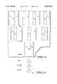
- FIG. 3includes a top view of a reticle that illustrates the use of outriggers for dense, semi-dense and isolated feature patterns.
- Attenuating features 30, as illustrated in FIG. 3are of a substantially uniform width. However, in alternative embodiments these widths can vary.
- the outriggers 32, 34, and 36are illustrated as having different line widths based on where the outriggers are located. Also, the three patterns have different pitches. Pitch is the distance that is the sum of a line width of an attenuating feature 30 and the distance between that feature 30 and the next adjacent feature 30.
- the three different feature patternshave different pitch-to-line width ratios.
- the dense feature patternhas a pitch-to-line width ratio no greater than approximately 3:1
- the isolated feature patternhas a pitch-to-line width ratio of at least 6:1
- the semi-dense feature patternhas a pitch-to-line width ratio between 3:1 and 6:1.
- the dense feature patternhas outriggers 32 that are relatively narrow because the pitch-to-line width ratio is relatively small compared to the semi-dense and isolated feature patterns.
- the outriggers 32are on both sides of the pattern.
- outriggers 34that are slightly wider to account for the larger pitch-to-line-width ratio in the semi-dense lines.
- Illustrated in the isolated feature patternare outriggers 36 that can be the same width or wider than the outriggers 32 or 34.
- the dense and semi-dense feature patternshave only one outrigger between each of the features 30. Compare this with the prior art, in which there are no outriggers between features within the dense or semi-dense feature patterns.
- each isolated featurehas two outriggers 36 adjacent to each of its opposing edges. Another portion of the device that would have an isolated feature may be 10 microns or more away from the isolated line and would similarly have a pair of outriggers 36 surrounding a different feature 30, but is not illustrated in FIG. 3. Therefore, as in the prior art for the isolated feature patterns, there could be two outriggers 36 that would lie between the widely spaced apart features 30.
- the present inventioncan be used for a wide variety of wavelengths of radiation sources, numerical aperture of lenses, and resist materials used in forming semiconductor devices.
- wavelengths usedcan range from approximately 436 nanometers (g-line) and lower.
- Other commonly used wavelengthsinclude approximately 356 nanometers (i-line), approximately 248 nanometers (deep ultraviolet or DUV), and approximately 193 nanometers (extreme ultraviolet or EUV).
- the numerical aperture of the lensesare generally in a range of approximately 0.45 to 0.65.
- the resist materialstypically are determined by the radiation source used, as the materials within the resist must be activated optimally at the wavelength of the radiation source used.
- Other resist materials, light source configurations, numerical apertures, and wavelengthscan be used.
- the present inventioncould be used for longer wavelength systems to extend their useful life before having to replace the equipment.
- the present inventioncan be used during the design and formation of a reticle.
- a semiconductor device layout fileis generated.
- the portions of the layout file corresponding to the attenuating features 30are made.
- the outriggerscan be manually or automatically inserted into the layout file after the locations of the attenuating features have been determined.
- the outriggerscan be scaled to the pitch-to-line-width ratio.
- the dense feature patternmay be seen with a memory array, and the semi-dense and isolated feature patterns may be used with logic portions of a semiconductor device.
- the layout filecan be transferred to a reticle fabrication tool, such as an electron beam writer.
- a reticle fabrication toolsuch as an electron beam writer.
- the layout fileis downloaded into a computer coupled to the reticle fabrication tool.
- a reticle substrateis processed to form a reticle having the pattern shown in FIG. 3.
- FIG. 3can be used to form a semiconductor device by exposing and developing a resist layer to give features similar to those shown in FIG. 4.
- FIG. 4includes an illustration of resist profiles. As can be seen, the width of the dense, semi-dense, and isolated features are substantially the same.
- a semiconductor device substrate 50includes field isolation regions 52, a gate dielectric layer 54, a conductive layer 56 and a resist layer 58.
- the semiconductor device substrate 50can be a monocrystalline semiconductor wafer, a semiconductor-on-insulating wafer, or any other substrate used to form semiconductor devices.
- Field isolation regions 52, the gate dielectric layer 54 and conductive layer 56are all formed using conventional processing steps.
- the conductive layer 56includes polysilicon, amorphous silicon, a silicide, or other metal-containing material.
- the resist layer 58is typically coated over the wafer and is spun on to achieve a relatively planar upper surface.
- Reticle 40includes a transparent substrate 42 made of quartz, glass, or the like and has attenuating features 30 and outriggers 32.
- the reticle 40is placed between the substrate 50 and the radiation source of a lithography tool (not illustrated) in FIG. 5 to emanate radiation 44 as illustrated in FIG. 5.
- the radiation 44does not pass through the features 30.
- the radiation 44is able to bend around the outriggers 32 to expose portions of the resist layer 58 beneath the transparent portions of the reticle 40 and underneath the outriggers 32.
- the features 30substantially block the radiation 44 from reaching the resist layer 58 below those features.
- the substrateis then removed from the lithography tool and the resist layer 58 is then developed using a conventional method. After developing, the resist layer 58 has members that overlie conductive layer 56 where gate electrodes will be formed as shown in FIG. 6.
- the substrateis then etched using a conventional etching step to form gate electrodes from the conductive layer 56. After etching to form the gate electrodes the resist members 58 are then removed using a conventional process.
- FIG. 7includes an illustration of the device at this point in the process.
- doped regions 62are formed in the substrate 50, and an interlevel dielectric layer 64 is then formed by deposition over the gate electrodes formed in conductive layer 56, doped regions 62 and field isolation regions 52.
- the interlevel dielectric layer 64may include doped oxide, undoped oxide, or a combination thereof.
- the interlevel dielectric layer 64is then patterned and interconnects 66 are formed to the doped regions 62. Other openings are made to the conductive layer 56 to connect the gate electrodes to other portions of the device but are not illustrated in FIG. 8.
- a passivation layer 68is then formed over the interconnects 66. In alternate embodiments, other contacts, interlevel dielectric layers, and interconnects may be formed as needed.
- the passivation layer 68overlies the uppermost interconnect level.
- the embodiments of the present inventioninclude a number of benefits.
- the outriggerscan be used at any pitch-to-line width ratio. Further, all features more closely replicate the dense feature pattern. Therefore, there is not a combination of characteristics that are unique to the dense, semi-dense and isolated feature patterns.
- the illumination conditionscan be optimized for a dense feature pattern since there will always be outriggers adjacent to each of the features. For example, annular illumination can be effectively used to improve processing latitude.
- a further benefit of the present inventionis that it can be used to extend the lifetime of existing equipment. More specifically, g-line steppers may be able to achieve a minimum lithography of approximately 0.8 microns. By the use of the outriggers, the minimum geometry may be extended down to 0.7 microns or possibly even lower.
- a further benefit of the present inventionis that it can be used over a widely varying set of lithography parameters including wavelength and numerical aperture of the lens.
- reticleshould be used in a manner that would be relatively transparent to process engineers and operators working within a wafer fabrication facility.
- the embodiments of the present inventioncan be used to form a semiconductor device using conventional lithography tools and processes.
- the parameters for using the lithography toolsare not expected to dramatically change, either the intensity of the light or the exposure time may increase slightly over that of the prior art since there are now more reticle features.
- these changesshould be less than 10% in magnitude and can be optimized as needed.
- the use of the present inventionis not expected to be a significant throughput limitation for the lithography tool which would otherwise cause an increase in the production costs of the wafers.
- Another benefit of the present inventionis that it can achieve a more consistent width of the developed resist features across the substrate surface whether the feature is found in a dense feature pattern, semi-dense feature pattern, or isolated feature pattern. This consistency in the width should still be maintained, even with small variations in the lithographic processing conditions.
- the embodiments of the present inventioncan be used for a number of different types of patterning layers.
- the present inventioncould be used to pattern a contact level or an interconnect level of the semiconductor device.
- the larger benefit of the present inventionis seen when forming masking levels that are considered critical. In other words, those that are designed to have features close to the resolution limit of the lithography tool.
- the present inventioncan be used for non-critical layers, such as some of the implant masks, the concepts of the present invention can be extended to the implant masks if needed.
- the embodiments of the present inventioncan be integrated to be used with phase shifting masks.
- the phase shifting materialcan be formed adjacent to the outriggers or attenuating features.
- the outriggersthemselves can be composed of phase edges (the edges between phase shifted and non-phase shifted regions on the reticle). These phase shifted outriggers can be made subresolution by having no or substantially less chrome than would a phase shifted feature.
- a second lithographic exposure stepcould be performed of the outrigger feature to ensure that those features do not print in the resist layer.
Landscapes
- Physics & Mathematics (AREA)
- General Physics & Mathematics (AREA)
- Exposure And Positioning Against Photoresist Photosensitive Materials (AREA)
Abstract
Description
Claims (34)
Priority Applications (1)
| Application Number | Priority Date | Filing Date | Title |
|---|---|---|---|
| US08/912,601US5827625A (en) | 1997-08-18 | 1997-08-18 | Methods of designing a reticle and forming a semiconductor device therewith |
Applications Claiming Priority (1)
| Application Number | Priority Date | Filing Date | Title |
|---|---|---|---|
| US08/912,601US5827625A (en) | 1997-08-18 | 1997-08-18 | Methods of designing a reticle and forming a semiconductor device therewith |
Publications (1)
| Publication Number | Publication Date |
|---|---|
| US5827625Atrue US5827625A (en) | 1998-10-27 |
Family
ID=25432169
Family Applications (1)
| Application Number | Title | Priority Date | Filing Date |
|---|---|---|---|
| US08/912,601Expired - LifetimeUS5827625A (en) | 1997-08-18 | 1997-08-18 | Methods of designing a reticle and forming a semiconductor device therewith |
Country Status (1)
| Country | Link |
|---|---|
| US (1) | US5827625A (en) |
Cited By (18)
| Publication number | Priority date | Publication date | Assignee | Title |
|---|---|---|---|---|
| US6042973A (en)* | 1998-01-08 | 2000-03-28 | Micron Technology, Inc. | Subresolution grating for attenuated phase shifting mask fabrication |
| US6096457A (en)* | 1998-02-27 | 2000-08-01 | Micron Technology, Inc. | Method for optimizing printing of a phase shift mask having a phase shift error |
| US6106979A (en)* | 1997-12-30 | 2000-08-22 | Micron Technology, Inc. | Use of attenuating phase-shifting mask for improved printability of clear-field patterns |
| US6184041B1 (en)* | 1998-05-13 | 2001-02-06 | International Business Machines Corporation | Fused hybrid resist shapes as a means of modulating hybrid resist space width |
| US6280646B1 (en) | 1999-07-16 | 2001-08-28 | Micron Technology, Inc. | Use of a chemically active reticle carrier for photomask etching |
| US6379847B2 (en) | 1998-02-27 | 2002-04-30 | Micron Technology, Inc. | Electrically programmable photolithography mask |
| KR100375146B1 (en)* | 1999-07-09 | 2003-03-29 | 엔이씨 일렉트로닉스 코포레이션 | Reticle and method of fabricating semiconductor device |
| US20030064298A1 (en)* | 2001-09-28 | 2003-04-03 | Asml Masktools, B.V. | Optical proximity correction method utilizing phase-edges as sub-resolution assist features |
| US6544694B2 (en)* | 2000-03-03 | 2003-04-08 | Koninklijke Philips Electronics N.V. | Method of manufacturing a device by means of a mask phase-shifting mask for use in said method |
| US6569574B2 (en)* | 1999-10-18 | 2003-05-27 | Micron Technology, Inc. | Methods of patterning radiation, methods of forming radiation-patterning tools, and radiation-patterning tools |
| US6582858B2 (en)* | 2001-09-07 | 2003-06-24 | United Microelectronics Corp. | Alternating phase shifting mask |
| US20030198873A1 (en)* | 2001-12-10 | 2003-10-23 | Dupont Photomasks, Inc. | Photomask and method for qualifying the same with a prototype specification |
| US20030211400A1 (en)* | 2000-02-14 | 2003-11-13 | Smith Bruce W | Method of improving photomask geometry |
| US6649452B2 (en)* | 2002-02-28 | 2003-11-18 | Motorola, Inc. | Method for manufacturing a lithographic reticle for transferring an integrated circuit design to a semiconductor wafer |
| US20040038134A1 (en)* | 2002-08-21 | 2004-02-26 | Dulman H. Daniel | Radiation-patterning tools, and methods of printing structures |
| US6737199B1 (en)* | 2000-01-31 | 2004-05-18 | Taiwan Semiconductor Manufacturing Company | Using new pattern fracturing rules for optical proximity correction mask-making to improve critical dimension uniformity |
| US20040248016A1 (en)* | 2003-06-06 | 2004-12-09 | Lucas Kevin D. | Method of designing a reticle and forming a semiconductor device therewith |
| DE10164306B4 (en)* | 2001-12-28 | 2006-06-08 | Infineon Technologies Ag | Double exposure with imaging auxiliary structures and different exposure tools |
Citations (5)
| Publication number | Priority date | Publication date | Assignee | Title |
|---|---|---|---|---|
| US4231811A (en)* | 1979-09-13 | 1980-11-04 | Intel Corporation | Variable thickness self-aligned photoresist process |
| US5242770A (en)* | 1992-01-16 | 1993-09-07 | Microunity Systems Engineering, Inc. | Mask for photolithography |
| US5286581A (en)* | 1991-08-19 | 1994-02-15 | Motorola, Inc. | Phase-shift mask and method for making |
| US5302477A (en)* | 1992-08-21 | 1994-04-12 | Intel Corporation | Inverted phase-shifted reticle |
| US5718829A (en)* | 1995-09-01 | 1998-02-17 | Micron Technology, Inc. | Phase shift structure and method of fabrication |
- 1997
- 1997-08-18USUS08/912,601patent/US5827625A/ennot_activeExpired - Lifetime
Patent Citations (5)
| Publication number | Priority date | Publication date | Assignee | Title |
|---|---|---|---|---|
| US4231811A (en)* | 1979-09-13 | 1980-11-04 | Intel Corporation | Variable thickness self-aligned photoresist process |
| US5286581A (en)* | 1991-08-19 | 1994-02-15 | Motorola, Inc. | Phase-shift mask and method for making |
| US5242770A (en)* | 1992-01-16 | 1993-09-07 | Microunity Systems Engineering, Inc. | Mask for photolithography |
| US5302477A (en)* | 1992-08-21 | 1994-04-12 | Intel Corporation | Inverted phase-shifted reticle |
| US5718829A (en)* | 1995-09-01 | 1998-02-17 | Micron Technology, Inc. | Phase shift structure and method of fabrication |
Non-Patent Citations (6)
| Title |
|---|
| Garofalo, et al., "Lithography Tricks and Tribulations", SPIE, vol. 2884, pp. 311-322, Jul. (1996). |
| Garofalo, et al., Lithography Tricks and Tribulations , SPIE, vol. 2884, pp. 311 322, Jul. (1996).* |
| Kenny, et al., "Chromeless Phase-Shifted Masks: A New Approach to Phase-Shifting Masks", A Preprint from the Tenth Annual Symposium on Microlithography of BACUS, pp. 1-12, Figs. 1-15, Sep. (1990). |
| Kenny, et al., Chromeless Phase Shifted Masks: A New Approach to Phase Shifting Masks , A Preprint from the Tenth Annual Symposium on Microlithography of BACUS, pp. 1 12, Figs. 1 15, Sep. (1990).* |
| Kim, et al. "CD Control for 180-nm and 130-nm Gate-Level Lithography", Microlithography World, pp. 16-21 (Autumn 1996). |
| Kim, et al. CD Control for 180 nm and 130 nm Gate Level Lithography , Microlithography World, pp. 16 21 (Autumn 1996).* |
Cited By (45)
| Publication number | Priority date | Publication date | Assignee | Title |
|---|---|---|---|---|
| US6106979A (en)* | 1997-12-30 | 2000-08-22 | Micron Technology, Inc. | Use of attenuating phase-shifting mask for improved printability of clear-field patterns |
| US6255024B1 (en) | 1997-12-30 | 2001-07-03 | Micron Technology, Inc. | Use of attenuating phase-shifting mask for improved printability of clear-field patterns |
| US6268091B1 (en) | 1998-01-08 | 2001-07-31 | Micron | Subresolution grating for attenuated phase shifting mask fabrication |
| US6077630A (en)* | 1998-01-08 | 2000-06-20 | Micron Technology, Inc. | Subresolution grating for attenuated phase shifting mask fabrication |
| US6558856B2 (en) | 1998-01-08 | 2003-05-06 | Micron Technology, Inc. | Subresolution grating for attenuated phase shifting mask fabrication |
| US6042973A (en)* | 1998-01-08 | 2000-03-28 | Micron Technology, Inc. | Subresolution grating for attenuated phase shifting mask fabrication |
| US6096457A (en)* | 1998-02-27 | 2000-08-01 | Micron Technology, Inc. | Method for optimizing printing of a phase shift mask having a phase shift error |
| US6379847B2 (en) | 1998-02-27 | 2002-04-30 | Micron Technology, Inc. | Electrically programmable photolithography mask |
| US6528217B2 (en) | 1998-02-27 | 2003-03-04 | Micron Technology, Inc. | Electrically programmable photolithography mask |
| US6537710B2 (en) | 1998-02-27 | 2003-03-25 | Micron Technology, Inc. | Electrically programmable photolithography mask |
| US6917411B1 (en) | 1998-02-27 | 2005-07-12 | Micron Technology, Inc. | Method for optimizing printing of an alternating phase shift mask having a phase shift error |
| US6184041B1 (en)* | 1998-05-13 | 2001-02-06 | International Business Machines Corporation | Fused hybrid resist shapes as a means of modulating hybrid resist space width |
| KR100375146B1 (en)* | 1999-07-09 | 2003-03-29 | 엔이씨 일렉트로닉스 코포레이션 | Reticle and method of fabricating semiconductor device |
| US6280646B1 (en) | 1999-07-16 | 2001-08-28 | Micron Technology, Inc. | Use of a chemically active reticle carrier for photomask etching |
| US6402886B2 (en) | 1999-07-16 | 2002-06-11 | Micron Technology, Inc. | Use of a chemically active reticle carrier for photomask etching |
| US6569574B2 (en)* | 1999-10-18 | 2003-05-27 | Micron Technology, Inc. | Methods of patterning radiation, methods of forming radiation-patterning tools, and radiation-patterning tools |
| US6692900B2 (en) | 1999-10-18 | 2004-02-17 | Micron Technology, Inc. | Methods of patterning radiation, methods of forming radiation-patterning tools, and radiation-patterning tools |
| US20040137342A1 (en)* | 1999-10-18 | 2004-07-15 | Bill Baggenstoss | Methods of patterning radiation, methods of forming radiation-patterning tools, and radiation-patterning tools |
| US7122453B2 (en) | 1999-10-18 | 2006-10-17 | Micron Technology, Inc. | Methods of patterning radiation, methods of forming radiation-patterning tools, and radiation-patterning tools |
| US6692876B2 (en) | 1999-10-18 | 2004-02-17 | Micron Technology, Inc. | Methods of patterning radiation, methods of forming radiation-patterning tools, and radiation-patterning tools |
| US6737199B1 (en)* | 2000-01-31 | 2004-05-18 | Taiwan Semiconductor Manufacturing Company | Using new pattern fracturing rules for optical proximity correction mask-making to improve critical dimension uniformity |
| US20030211400A1 (en)* | 2000-02-14 | 2003-11-13 | Smith Bruce W | Method of improving photomask geometry |
| JP2010079303A (en)* | 2000-02-14 | 2010-04-08 | Asml Masktools Bv | Method of improving photomask geometry |
| EP1269266A4 (en)* | 2000-02-14 | 2005-08-24 | Asml Masktools Bv | A method of improving photomask geometry |
| US6846595B2 (en)* | 2000-02-14 | 2005-01-25 | Asml Netherlands B.V. | Method of improving photomask geometry |
| US6544694B2 (en)* | 2000-03-03 | 2003-04-08 | Koninklijke Philips Electronics N.V. | Method of manufacturing a device by means of a mask phase-shifting mask for use in said method |
| US6582858B2 (en)* | 2001-09-07 | 2003-06-24 | United Microelectronics Corp. | Alternating phase shifting mask |
| US20030064298A1 (en)* | 2001-09-28 | 2003-04-03 | Asml Masktools, B.V. | Optical proximity correction method utilizing phase-edges as sub-resolution assist features |
| US7399559B2 (en) | 2001-09-28 | 2008-07-15 | Asml Masktools B.V. | Optical proximity correction method utilizing phase-edges as sub-resolution assist features |
| EP1298489A3 (en)* | 2001-09-28 | 2003-08-27 | ASML Masktools B.V. | An optical proximity correction method utilizing phase-edges as sub-resolution assist features |
| US7026081B2 (en) | 2001-09-28 | 2006-04-11 | Asml Masktools B.V. | Optical proximity correction method utilizing phase-edges as sub-resolution assist features |
| US20050271953A1 (en)* | 2001-09-28 | 2005-12-08 | Asml Masktools B.V. | Optical proximity correction method utilizing phase-edges as sub-resolution assist features |
| WO2003050615A3 (en)* | 2001-12-10 | 2004-02-12 | Dupont Photomasks Inc | Photomask and method for qualifying the same with a prototype specification |
| US6910203B2 (en)* | 2001-12-10 | 2005-06-21 | Toppan Photomasks, Inc. | Photomask and method for qualifying the same with a prototype specification |
| CN100380381C (en)* | 2001-12-10 | 2008-04-09 | 凸版光掩膜公司 | Photomask and method for qualifying it with template specification |
| US20030198873A1 (en)* | 2001-12-10 | 2003-10-23 | Dupont Photomasks, Inc. | Photomask and method for qualifying the same with a prototype specification |
| DE10164306B4 (en)* | 2001-12-28 | 2006-06-08 | Infineon Technologies Ag | Double exposure with imaging auxiliary structures and different exposure tools |
| US6649452B2 (en)* | 2002-02-28 | 2003-11-18 | Motorola, Inc. | Method for manufacturing a lithographic reticle for transferring an integrated circuit design to a semiconductor wafer |
| US6911301B2 (en)* | 2002-08-21 | 2005-06-28 | Micron Technology, Inc. | Methods of forming aligned structures with radiation-sensitive material |
| US6887629B2 (en) | 2002-08-21 | 2005-05-03 | Micron Technology, Inc. | Radiation-patterning tool |
| US20040180272A1 (en)* | 2002-08-21 | 2004-09-16 | Dulman H. Daniel | Methods of printing structures |
| US20040180273A1 (en)* | 2002-08-21 | 2004-09-16 | Dulman H. Daniel | Methods of forming aligned structures with radiation-sensitive material |
| US20040038134A1 (en)* | 2002-08-21 | 2004-02-26 | Dulman H. Daniel | Radiation-patterning tools, and methods of printing structures |
| US7226707B2 (en) | 2002-08-21 | 2007-06-05 | Micron Technology, Inc. | Methods of printing structures |
| US20040248016A1 (en)* | 2003-06-06 | 2004-12-09 | Lucas Kevin D. | Method of designing a reticle and forming a semiconductor device therewith |
Similar Documents
| Publication | Publication Date | Title |
|---|---|---|
| US5827625A (en) | Methods of designing a reticle and forming a semiconductor device therewith | |
| US7036108B2 (en) | Full sized scattering bar alt-PSM technique for IC manufacturing in sub-resolution era | |
| US7659042B2 (en) | Full phase shifting mask in damascene process | |
| US7737016B2 (en) | Two-print two-etch method for enhancement of CD control using ghost poly | |
| US20040248016A1 (en) | Method of designing a reticle and forming a semiconductor device therewith | |
| KR101147194B1 (en) | System and method for fabricating contact holes | |
| EP1752825B1 (en) | Lithography Masks and Methods | |
| US20040234900A1 (en) | Method and apparatus for producing rectangular contact holes utilizing side lobe formation | |
| JP2004514171A (en) | Photolithography mask | |
| US6902851B1 (en) | Method for using phase-shifting mask | |
| US5837426A (en) | Photolithographic process for mask programming of read-only memory devices | |
| US20110191728A1 (en) | Integrated circuit having line end created through use of mask that controls line end shortening and corner rounding arising from proximity effects | |
| EP1488284B1 (en) | Photomask and method for photolithographic patterning of a substrate by use of phase shifted assist features | |
| EP1288721B1 (en) | Photolithography with multiple level substrate | |
| US6620564B2 (en) | Method for patterning semiconductors through adjustment of image peak side lobes | |
| US6924069B2 (en) | Method for repairing attenuated phase shift masks | |
| US6406819B1 (en) | Method for selective PSM with assist OPC | |
| US20070015088A1 (en) | Method for lithographically printing tightly nested and isolated hole features using double exposure | |
| KR100278917B1 (en) | Method for manufacturing contact mask of semiconductor device | |
| US6911301B2 (en) | Methods of forming aligned structures with radiation-sensitive material | |
| US7008729B2 (en) | Method for fabricating phase mask of photolithography process | |
| KR100223324B1 (en) | Fine structure pattern fabricating method of semiconductor | |
| KR20040006323A (en) | Method for manufacturing reticle |
Legal Events
| Date | Code | Title | Description |
|---|---|---|---|
| AS | Assignment | Owner name:MOTOROLA, INC., ILLINOIS Free format text:ASSIGNMENT OF ASSIGNORS INTEREST;ASSIGNORS:LUCAS, KEVIN;KLING, MICHAEL E.;ROMAN, BERNARD J.;AND OTHERS;REEL/FRAME:008769/0247 Effective date:19970814 | |
| STCF | Information on status: patent grant | Free format text:PATENTED CASE | |
| FPAY | Fee payment | Year of fee payment:4 | |
| AS | Assignment | Owner name:FREESCALE SEMICONDUCTOR, INC., TEXAS Free format text:ASSIGNMENT OF ASSIGNORS INTEREST;ASSIGNOR:MOTOROLA, INC.;REEL/FRAME:015698/0657 Effective date:20040404 Owner name:FREESCALE SEMICONDUCTOR, INC.,TEXAS Free format text:ASSIGNMENT OF ASSIGNORS INTEREST;ASSIGNOR:MOTOROLA, INC.;REEL/FRAME:015698/0657 Effective date:20040404 | |
| FPAY | Fee payment | Year of fee payment:8 | |
| AS | Assignment | Owner name:CITIBANK, N.A. AS COLLATERAL AGENT, NEW YORK Free format text:SECURITY AGREEMENT;ASSIGNORS:FREESCALE SEMICONDUCTOR, INC.;FREESCALE ACQUISITION CORPORATION;FREESCALE ACQUISITION HOLDINGS CORP.;AND OTHERS;REEL/FRAME:018855/0129 Effective date:20061201 Owner name:CITIBANK, N.A. AS COLLATERAL AGENT,NEW YORK Free format text:SECURITY AGREEMENT;ASSIGNORS:FREESCALE SEMICONDUCTOR, INC.;FREESCALE ACQUISITION CORPORATION;FREESCALE ACQUISITION HOLDINGS CORP.;AND OTHERS;REEL/FRAME:018855/0129 Effective date:20061201 | |
| FPAY | Fee payment | Year of fee payment:12 | |
| AS | Assignment | Owner name:CITIBANK, N.A., AS COLLATERAL AGENT,NEW YORK Free format text:SECURITY AGREEMENT;ASSIGNOR:FREESCALE SEMICONDUCTOR, INC.;REEL/FRAME:024397/0001 Effective date:20100413 Owner name:CITIBANK, N.A., AS COLLATERAL AGENT, NEW YORK Free format text:SECURITY AGREEMENT;ASSIGNOR:FREESCALE SEMICONDUCTOR, INC.;REEL/FRAME:024397/0001 Effective date:20100413 | |
| AS | Assignment | Owner name:CITIBANK, N.A., AS NOTES COLLATERAL AGENT, NEW YORK Free format text:SECURITY AGREEMENT;ASSIGNOR:FREESCALE SEMICONDUCTOR, INC.;REEL/FRAME:030633/0424 Effective date:20130521 Owner name:CITIBANK, N.A., AS NOTES COLLATERAL AGENT, NEW YOR Free format text:SECURITY AGREEMENT;ASSIGNOR:FREESCALE SEMICONDUCTOR, INC.;REEL/FRAME:030633/0424 Effective date:20130521 | |
| AS | Assignment | Owner name:CITIBANK, N.A., AS NOTES COLLATERAL AGENT, NEW YORK Free format text:SECURITY AGREEMENT;ASSIGNOR:FREESCALE SEMICONDUCTOR, INC.;REEL/FRAME:031591/0266 Effective date:20131101 Owner name:CITIBANK, N.A., AS NOTES COLLATERAL AGENT, NEW YOR Free format text:SECURITY AGREEMENT;ASSIGNOR:FREESCALE SEMICONDUCTOR, INC.;REEL/FRAME:031591/0266 Effective date:20131101 | |
| AS | Assignment | Owner name:FREESCALE SEMICONDUCTOR, INC., TEXAS Free format text:PATENT RELEASE;ASSIGNOR:CITIBANK, N.A., AS COLLATERAL AGENT;REEL/FRAME:037356/0553 Effective date:20151207 Owner name:FREESCALE SEMICONDUCTOR, INC., TEXAS Free format text:PATENT RELEASE;ASSIGNOR:CITIBANK, N.A., AS COLLATERAL AGENT;REEL/FRAME:037354/0225 Effective date:20151207 Owner name:FREESCALE SEMICONDUCTOR, INC., TEXAS Free format text:PATENT RELEASE;ASSIGNOR:CITIBANK, N.A., AS COLLATERAL AGENT;REEL/FRAME:037356/0143 Effective date:20151207 | |
| AS | Assignment | Owner name:MORGAN STANLEY SENIOR FUNDING, INC., MARYLAND Free format text:ASSIGNMENT AND ASSUMPTION OF SECURITY INTEREST IN PATENTS;ASSIGNOR:CITIBANK, N.A.;REEL/FRAME:037486/0517 Effective date:20151207 | |
| AS | Assignment | Owner name:MORGAN STANLEY SENIOR FUNDING, INC., MARYLAND Free format text:ASSIGNMENT AND ASSUMPTION OF SECURITY INTEREST IN PATENTS;ASSIGNOR:CITIBANK, N.A.;REEL/FRAME:037518/0292 Effective date:20151207 | |
| AS | Assignment | Owner name:MORGAN STANLEY SENIOR FUNDING, INC., MARYLAND Free format text:SUPPLEMENT TO THE SECURITY AGREEMENT;ASSIGNOR:FREESCALE SEMICONDUCTOR, INC.;REEL/FRAME:039138/0001 Effective date:20160525 | |
| AS | Assignment | Owner name:NXP, B.V., F/K/A FREESCALE SEMICONDUCTOR, INC., NETHERLANDS Free format text:RELEASE BY SECURED PARTY;ASSIGNOR:MORGAN STANLEY SENIOR FUNDING, INC.;REEL/FRAME:040925/0001 Effective date:20160912 Owner name:NXP, B.V., F/K/A FREESCALE SEMICONDUCTOR, INC., NE Free format text:RELEASE BY SECURED PARTY;ASSIGNOR:MORGAN STANLEY SENIOR FUNDING, INC.;REEL/FRAME:040925/0001 Effective date:20160912 | |
| AS | Assignment | Owner name:NXP B.V., NETHERLANDS Free format text:RELEASE BY SECURED PARTY;ASSIGNOR:MORGAN STANLEY SENIOR FUNDING, INC.;REEL/FRAME:040928/0001 Effective date:20160622 | |
| AS | Assignment | Owner name:NXP USA, INC., TEXAS Free format text:CHANGE OF NAME;ASSIGNOR:FREESCALE SEMICONDUCTOR INC.;REEL/FRAME:040652/0180 Effective date:20161107 | |
| AS | Assignment | Owner name:NXP USA, INC., TEXAS Free format text:CORRECTIVE ASSIGNMENT TO CORRECT THE NATURE OF CONVEYANCE LISTED CHANGE OF NAME SHOULD BE MERGER AND CHANGE PREVIOUSLY RECORDED AT REEL: 040652 FRAME: 0180. ASSIGNOR(S) HEREBY CONFIRMS THE MERGER AND CHANGE OF NAME;ASSIGNOR:FREESCALE SEMICONDUCTOR INC.;REEL/FRAME:041354/0148 Effective date:20161107 | |
| AS | Assignment | Owner name:MORGAN STANLEY SENIOR FUNDING, INC., MARYLAND Free format text:CORRECTIVE ASSIGNMENT TO CORRECT THE REMOVE PATENTS 8108266 AND 8062324 AND REPLACE THEM WITH 6108266 AND 8060324 PREVIOUSLY RECORDED ON REEL 037518 FRAME 0292. ASSIGNOR(S) HEREBY CONFIRMS THE ASSIGNMENT AND ASSUMPTION OF SECURITY INTEREST IN PATENTS;ASSIGNOR:CITIBANK, N.A.;REEL/FRAME:041703/0536 Effective date:20151207 | |
| AS | Assignment | Owner name:SHENZHEN XINGUODU TECHNOLOGY CO., LTD., CHINA Free format text:CORRECTIVE ASSIGNMENT TO CORRECT THE TO CORRECT THE APPLICATION NO. FROM 13,883,290 TO 13,833,290 PREVIOUSLY RECORDED ON REEL 041703 FRAME 0536. ASSIGNOR(S) HEREBY CONFIRMS THE THE ASSIGNMENT AND ASSUMPTION OF SECURITYINTEREST IN PATENTS.;ASSIGNOR:MORGAN STANLEY SENIOR FUNDING, INC.;REEL/FRAME:048734/0001 Effective date:20190217 | |
| AS | Assignment | Owner name:NXP B.V., NETHERLANDS Free format text:RELEASE BY SECURED PARTY;ASSIGNOR:MORGAN STANLEY SENIOR FUNDING, INC.;REEL/FRAME:050744/0097 Effective date:20190903 | |
| AS | Assignment | Owner name:MORGAN STANLEY SENIOR FUNDING, INC., MARYLAND Free format text:CORRECTIVE ASSIGNMENT TO CORRECT THE REMOVE APPLICATION11759915 AND REPLACE IT WITH APPLICATION 11759935 PREVIOUSLY RECORDED ON REEL 037486 FRAME 0517. ASSIGNOR(S) HEREBY CONFIRMS THE ASSIGNMENT AND ASSUMPTION OF SECURITYINTEREST IN PATENTS;ASSIGNOR:CITIBANK, N.A.;REEL/FRAME:053547/0421 Effective date:20151207 | |
| AS | Assignment | Owner name:NXP B.V., NETHERLANDS Free format text:CORRECTIVE ASSIGNMENT TO CORRECT THE REMOVEAPPLICATION 11759915 AND REPLACE IT WITH APPLICATION11759935 PREVIOUSLY RECORDED ON REEL 040928 FRAME 0001. ASSIGNOR(S) HEREBY CONFIRMS THE RELEASE OF SECURITYINTEREST;ASSIGNOR:MORGAN STANLEY SENIOR FUNDING, INC.;REEL/FRAME:052915/0001 Effective date:20160622 | |
| AS | Assignment | Owner name:NXP, B.V. F/K/A FREESCALE SEMICONDUCTOR, INC., NETHERLANDS Free format text:CORRECTIVE ASSIGNMENT TO CORRECT THE REMOVEAPPLICATION 11759915 AND REPLACE IT WITH APPLICATION11759935 PREVIOUSLY RECORDED ON REEL 040925 FRAME 0001. ASSIGNOR(S) HEREBY CONFIRMS THE RELEASE OF SECURITYINTEREST;ASSIGNOR:MORGAN STANLEY SENIOR FUNDING, INC.;REEL/FRAME:052917/0001 Effective date:20160912 |