US5825658A - Method and a system for specifying and automatically analyzing multiple clock timing constraints in a VLSI circuit - Google Patents
Method and a system for specifying and automatically analyzing multiple clock timing constraints in a VLSI circuitDownload PDFInfo
- Publication number
- US5825658A US5825658AUS08/528,660US52866095AUS5825658AUS 5825658 AUS5825658 AUS 5825658AUS 52866095 AUS52866095 AUS 52866095AUS 5825658 AUS5825658 AUS 5825658A
- Authority
- US
- United States
- Prior art keywords
- timing
- timing constraints
- constraint
- clock
- integrated circuit
- Prior art date
- Legal status (The legal status is an assumption and is not a legal conclusion. Google has not performed a legal analysis and makes no representation as to the accuracy of the status listed.)
- Expired - Lifetime
Links
Images


Classifications
- G—PHYSICS
- G06—COMPUTING OR CALCULATING; COUNTING
- G06F—ELECTRIC DIGITAL DATA PROCESSING
- G06F30/00—Computer-aided design [CAD]
- G06F30/30—Circuit design
- G06F30/32—Circuit design at the digital level
- G06F30/33—Design verification, e.g. functional simulation or model checking
- G06F30/3308—Design verification, e.g. functional simulation or model checking using simulation
- G06F30/3312—Timing analysis
Definitions
- the present inventionis related generally to integrated circuit simulation and circuit optimization, and is particularly related to systems and methods for specifying multi-cycle timing constraints in very large scale integrated (VLSI) circuits for purposes of circuit simulation and circuit optimization.
- VLSIvery large scale integrated
- Timing constraintThe meaning of a timing constraint will be reviewed and then the syntax and semantics of the COMPASS timing constraint constructs will be introduced.
- a timing constraintspecifies a delay between specified nodes in a specified circuit.
- the specified delaycan be a minimum delay or a maximum delay.
- the specified delayis a minimum delay we speak about a "minDelay” timing constraint or a lower-bounded timing constraint.
- the specified delayis a maximum delay we speak about a "maxDelay” timing constraint or a upper-bounded timing constraint.
- a maxDelay timing constraintis composed of:
- a signal maximum arrival timethat is the latest time at which a signal is available on that node
- a signal maximum required timethat is the latest time at which a signal should be available on that node
- a minDelay timing constraintis composed of:
- a signal minimum arrival timethat is the earliest time at which a signal is available on that node
- a signal minimum required timethat is the earliest time at which a signal should be available on that node.
- Timing constraintsare used for at least the two following different reasons:
- Timing a timing constraintconsists in propagating a timing constraint input node arrival time value through a simulated representation of the specified circuit and comparing the value of the propagated time and the required time on the timing constraint's output node.
- slackis defined to mean the difference between the required time and the arrival time for any specified timing constraint output node.
- minDelay timing constraintthe term “slack” is defined to mean the difference between the arrival time and the required time for any specified timing constraint output node.
- a circuit designis said to be violating a timing constraint when at least one of the timing constraint output node's slack is negative.
- timing constraints for a specified circuitThere are many possible origins for timing constraints for a specified circuit. Some examples are:
- the environment in which the specified circuit is to be usedmay force some arrival times on an external input connector and may require various signals to be ready at specified "required times" on an output connector;
- the clock frequency and phase used by the specified circuitmay dictate the arrival times of sequentially generated output data at the circuit's output ports and may also dictate the required time of input data at the circuit's input connector;
- a desired clock latencymay require at particular signal arrival time on one or more clocked input nodes and/or may result in a particular required time on one or more particular output nodes.
- ff1will be called the master flip-flop
- ck1will be called the master clock
- ck2will be called the slave clock
- the shortest combinational path between the ff1 data output connector to the ff2 data input connectorwill be called shortest path; this path is really composed of the ff1 ck1-to-q timing plus the combinational path minus the ff2 hold time;
- the longest combinational path between the ff1 data output connector to the ff2 data input connectorwill be called the longest path; this path really is composed of the ff1 ck1-to-q timing plus the combinational path plus the ff2 set up time.
- a launch edgeis an active edge of the master clock and a latch edge is an active edge of the slave clock.
- a "setup check”checks setup relations between a pair of flip-flops; a setup relation tells that the correct data signal value is stable on the slave flip-flop in time to be properly latched.
- a setup relationthus determines one setup launch edge among the list of the launch edges and one set up latch edge among the list of latch edges.
- the difference between the setup latch edge and setup launch edgeimplies a maximum delay constraint for the longest path starting on a master flip-flop and ending on a slave flip-flop.
- the setup relationis simple: it checks the longest path between a pair of flip-flops clocked on the same pair of flip-flops.
- the setup checkfirst looks for the smallest difference between the setup latch edges and the setup launch edges. It then checks that the longest path is smaller than that difference.
- hold relationsare checked around all the different setup relations detected by the setup check as follows:
- FIG. 3Ashows the hold relations on a single frequency design.
- FIG. 3Bpresents the hold relation on a multi-frequency design.
- multi-cycle clock timing constraint specification mechanismis a general mechanism which allows the user to escape the default detected setup edge and allows the circuit designer or test engineer to redefine the timing relationships being tested. More accurately, multi-cycle timing constraints allow the engineer:
- setup multiplierwhich usually is the number of slave active edges you want to add to the default setup latch edge for setup checking; if you do not "multi-cycle the clock," the default number is obviously one. More particularly, setting a setup multiplier of "n” pushes forward the setup latch edge by an amount of "n-1” slave clock cycles.
- the setup multipliercan also be specified as the number of master active edges you want to remove from the default setup launch edge. In this case, setting a setup multiplier of "n” consists in pushing backward the setup launch edge by an amount of "n-1" master clock cycles;
- a hold multiplierwhich usually is the number of master active edges you want to add to the default detected hold setup edge.
- the default numberis zero, whether the slave clock is multi-cycled or not.
- Setting a hold multiplier of "n”pushes forward the setup launch edge by a quantity of "n” master clock cycle.
- the hold multipliercan also be specified as the number of slave active edges you want to remove from the setup latch edge; in this later case, setting a hold multiplier of "n” consists in pushing backward the setup latch edge by a quantity of "n” slave clock cycle.
- FIG. 4Apresents a single frequency design with a setup multi-frequency design of two and a hold multiplier of zero on the slave flop.
- FIG. 4Bpresents a multi-frequency design with setup multiplier of two and a hold multiplier of zero on the slave clock.
- the circuit design engineer or test engineerknow that some flip-flops will be disabled. For instance, in case of the single-frequency design, if both the master and the slave flip-flops are disabled on the second active edge, the hold check procedure can be programmed to take that into account by specifying a hold multiplier of one (see FIGS. 5A and 5B). In case of the multi-frequency design, if you know that the slave flip-flop is disabled on the second active edge of the slave clock, you may also tell it to the hold checker by setting a hold multiplier of one.
- the list of nodes to specifyis "design-specific", that is the list of input nodes should contain the names of all the sequential elements clocked by the clock.
- design-specificthat is the list of input nodes should contain the names of all the sequential elements clocked by the clock.
- the list of nodes to specifyis "technology specific", that is the list of nodes contains the name of the data connector of the sequential elements, such as "q”, “qn”, "d", “da”, “db”, "s”.
- Timing constraintsare independent of each other.
- a timing constraintcan never relax another timing constraint: the worst or most difficult timing constraint (the tightest one) always "wins" in that it is the one which will be the basis for determining if a circuit design meets all timing constraints, or will be the basis for implementing or optimizing a circuit design if the timing constraints are being used with a circuit optimization tool.
- a path clustermatches the timing constraint definition described above. Basically to specify a path cluster, the user must:
- a clock constraint on a design nodespecifies a timing constraint whose input nodes are the data output connectors of sequential elements clocked on the specified node and whose output nodes are the data input connectors of sequential elements clocked on the specified node.
- To create a clock constraintthe user must declare a clock together with its attribute (e.g., period, waveform, latency, skew, . . . ) on a specified circuit node.
- An example of a clock constraintis:
- input nodesare the data output connectors of the sequential element clocked by the clock clk;
- output nodesare the data input connectors of the sequential element clocked by the clock clk;
- output maximum required timesare the specified period values (in this case 10 ns) minus the setup time of these sequential element data input connectors;
- the clock declarationcreates exactly the same timing constraint as explained above.
- the clock-relative external delaycompletes the timing constraint with:
- the clock declarationcreates exactly the same timing constraint as explained above.
- the clock-relative external delaycompletes the timing constraint with:
- the input nodes and output nodes for "clock timing constraints"are the data input and output connectors of sequential element clocked by that clock. If a specified circuit design has more than one clock, creating the timing constraints for each of the different clocks does not automatically constrain paths starting on one flip-flop's input connector clocked on one clock and ending on another flip-flop's output connector clocked on another clock. To constrain such paths, the user must create the different clocks, and then must "group” these clocks. Two clocks are "grouped" by using the following command:
- input nodeswill either be data output connectors of sequential data elements clocked on the master clock or external input connectors for which external input delays have been specified relative to the master clock;
- output nodeswill either be data input connectors of sequential data elements clocked on slave-clock or external output connectors for which external output delays have been specified on the slave clock;
- the arrival time and required timesare computed according to the setup and hold relations, determined as explained above in the section "CLOCKED DESIGNS".
- the userfirst creates a clock timing constraint with the appropriate period. This will constrain the adder and the multiplier to the same timing constraint.
- the multiplier output nodescan be removed from the clock timing constraint and a new timing constraint can be created with a double period as its required time by using a multi-cycle timing constraint:
- input nodesare the multi-cycle start point (ff1.dataoutput( ) and ff2.dataoutput( ));
- output nodesare the multi-cycle end point (ff3.datainput( ) and ff4.datainput( ));
- output node maximum required timeis the twice the period minus the sequential element setup time.
- This "set multiCycle" commandsremove the multi-cycle end nodes from the clock constraint. This is necessary, because otherwise these end nodes would still be optimized within the clock constraint, making the multi-cycle constraint useless. Moreover this will not remove the multi-cycle start nodes from the clock constraint; that is the multi-cycle start nodes will belong to both the multi-cycle constraint and the clock constraint. Furthermore, the same clock output node can be used in more than one multi-cycle constraint.
- ff1 and ff2have to be clocked on clk1 and ff3 and ff4 on clk2, otherwise nothing will be constrained.
- FIG. 6presents a typical multi-cycle design, referred to in the following as a "MCD design".
- the MCD original designis composed of one adder and one multiplier surrounded by flip-flops clocked on the same clock "clk".
- the multiplieris twice as slow as the adder.
- timing constraint createdis the one represented by the following table:
- timing constraintresults in the complete logic begin constrained on twice the clock period (20 ns). However, the timing constraint should provide a required time of 10 ns at ff4.d when the multiplexer u1 directs the adder output to flip-flop ff4.
- the value "5" of the output delayhas to be specified by the user and is computed assuming a delay of 5 ns from the multiplexer input to the data input of flip-flop ff4.
- Another trivial but inconvenient solutionis to enter one time constraint at a time, break the path through which the constraint should not be propagated and optimize the circuit design with that constraint. This is a difficult and error-prone process because for each iteration of the process the user must break all the paths through which the constraint should not be propagates, and must correctly specify the timing constraint for the path through which the constraint should be propagated.
- It is a primary object of the present inventionis to provide the user of both electronic circuit synthesis tools and electronic circuit timing verification tools with an improved system for specifying multi-cycle timing constraints in circuit designs.
- Another object of the present inventionis to provide a method for specifying and automatically analyzing multiple clock cycle timing constraints in a VLSI circuit.
- the present inventionprovides a system and method for specifying and using a "constraint-based through path", which is a way to both:
- timing pathsalso called signal paths
- the "constraint-based through path”can be specified at either the circuit level, or at the HDL level before the circuit design is synthesized.
- the "constraint specific through path”is composed of:
- timingArcis a pin-to-pin timing path through one gate.
- the method of the present inventioncomprises the following steps:
- a system employing the present invention systemwhich uses the previously summarized method, comprises constraint-base thou path means, and checks the correct timing behavior of a circuit according to that specification.
- the method of the present inventionallows the user to correctly specify the timing constraints for a specified circuit design and to thereby provide the timing information required for optimal operation of a circuit synthesis tool or circuit timing verification tool, taking into account multi-cycle timing constraints.
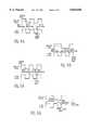
- FIGS. 1, 2A, 2B, 3A, 3B, 4A, 4B, 5A, 5Billustrate general knowledge in the domain of specifying "timing constraints" for electronic circuit designs.
- FIG. 6shows a typical multi-cycle circuit design
- FIG. 7shows an implementation of the circuit design represented in FIG. 6.
- FIGS. 8 and 9are used to illustrate the method of the present invention.
- FIGS. 10 and 11illustrates two examples using the method of the present invention.
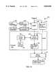
- FIG. 12is a flow diagram showing the flow of information in a preferred embodiment of the present invention.
- FIG. 13is a block diagram of a computer aided design system incorporating the present invention.
- FIG. 14schematically depicts the features of one circuit element or gate that are used in the path-based timing constraint generation procedure of the present invention.
- FIG. 15depicts a data structure for representing system level timing constraints.
- the computer aided circuit design (CAD) system 100 of the present inventionreceives a circuit netlist 102 from any of a number of sources.
- the circuit netlist 102may be directly generated and input by an engineer, or it may be generated by a logic synthesizer 104 from a set of logic equations 106 prepared by an engineer, or it may be generated by an HDL circuit synthesizer 108 from an HDL circuit description 110 written by an engineer.
- the engineerwill also generally specify a set of high level timing constraints 114 for the circuit as well as a cell library 116 for implementing the specified circuit with a particular set of circuit cells.
- the high level timing constraints 114are typically specified by the engineer as a set of input signal timing values (i.e., input nodes and a start time for each input node) and a set of output signal timing values (i.e., output nodes and a required arrival time for each output node).
- the delay parameters of each cell in the circuit netlistare obtained from the specified cell library 116, as discussed above.
- Netlist annotator procedure 118in conjunction with timing verifier 120, generates a set of path-based constraints from the circuit netlist 102 and the high level timing constraints.
- the path-based constraintsare stored in a path-based constraint file 122, and then passed to a timing driven silicon compiler 124 along with the circuit netlist 102.
- the silicon compiler 124generates a circuit layout 126 that satisfies the timing constraints specified in the path-based constraint file 122, or an error message if it is unable to generate a circuit layout meeting those timing constraints.
- the preferred embodimentis implemented on a computer workstation 140 having a CPU 162, a user interface 144, disk or other memory storage 146 for storing the cell library 116, netlist annotator 118 and timing verifier 120, as well as other software modules.
- Random access memory 148is used to store arrays of data such as the specified circuit netlist 102, an array of system level timing constraints 114, a file 122 of the path-based timing constraints generated by the netlist annotator 118, and node data structures 150 used during the process of generating the path-based timing constraints.
- Data such as the netlist 102, high level timing constraints 114 and the likemay be entered either through an input port 154 or through the user interface 144.
- the resulting file 122is transmitted via port 156 to a silicon compiler or connection routing program 122.
- the silicon compiler 124may be any one of several commercially available silicon compilers that utilize path-based timing constraints, including the Compass Design cellCOmplier, by Compass Design Automation of San Jose, Calif.
- each circuit element in a specified circuitis treated as a "box” or “gate” having inputs, outputs, pin-to-pin arcs connecting various ones of the input to various ones of the outputs, and a time delay value associated with each pin-to-pin arc. No other characteristics of the circuit elements are relevant to the procedure for generating path-based timing constraints.
- the system level timing constraintsare stored in a data structure 114 that represents multiple sets of distinct timing constraints.
- Each distinct constraintis represented by a set of start nodes (otherwise called input nodes), a start time for each such start node, a set of end nodes (otherwise known as output nodes) and a required arrival time for each such end node.
- Multiple system level timing constraintsare often used to represent distinct timing requirements associated with a specified circuit's performance.
- Data structure 114is also used to store the clock timing constraints and the constraint based "set through" specifications of the present invention.
- the method of the present inventionlets the user specify different timing constraints for different signal paths through a circuit.
- the timing paths between, ff1 and ff3 on the one side of the multiplexer and ff4 the other side of the multiplexershould be one clock period or two clock periods, respectively.
- the timing constraint to applydepends on the multiplexer selection bit value.
- the user of a circuit analysis tool for verifying that a circuit meets specified timing constraintsand the user of a circuit synthesis tool that optimizes a circuit design to as to meet specified timing constraints, both need a way to specify different timing constraints for different signal paths through a circuit.
- the specification of signal path specific timing constraintsis accomplished through the use of a construct called a "constraint specific through path".
- a "constraint specific through path”is composed of:
- timingArcis a pin-to-pin timing path through one gate.
- a timing arc driving a toNodeis broken for the specified constraint if it is not in the transitive fanout of a fromNode.
- a "constraint specific through path”is specified with the help of the following construct:
- ⁇ fromNodeNameList>specifies a list of nodes
- ⁇ toNodeNameList>specifies a list of nodes
- constraint ⁇ constraintName>specifies the constraint for which the "through” path applies.
- step 1we specify the clock timing constraint; this applies a 10 ns timing constraint to all the logic circuitry between the input nodes ff1.q, ff3.q and the output node ff4.d.
- Second (step 2)specifies a first multi-cycle timing constraint, mc1, for the multiplier.
- step 3specifies a "through" path u1.i2 ⁇ u1.z for the first multi-cycle timing constraint so that this timing constraint does not apply to the adder's signal path through the mulitplexer u1.i1 ⁇ u1.z.
- the multiplier in the first multi-cycle timing constraintunfortunately removes the ff4.d output node from the clock timing constraint.
- the direct consequenceis that the adder is also no longer subject to the one clock period timing constraint. That is, while the adder is driven by the clock constraint input nodes (ff1.q and ff3.q), it does not have any output nodes to which the timing constraint applies.
- the fourth phase (step 4)thus consists in creating a second multi-cycle timing constraint for the adder. Note that the multiplier factor of that multi-cycle is "1".
- the adder's multi-cycle timing constraintunfortunately applies a one clock period constraint to the complete combinational block composed of both the adder and the multiplier.
- the second multi-cycle timing constraintis thereby superseding the effect of the multiplier multi-cycle because it is applying a more stringent timing constraint.
- circuit nodes driving the multiplexerare named.
- the circuit nodes driving the multiplexercan be named by slightly modify the previously shown VHDL circuit description to read as follows:
- the userdoes not need to know the timing delay values of the circuit logic after the multiplexer
- circuit designwill be correctly optimized even if the logic after the multiplexer is modified during a circuit timing optimization process
- the method of the present inventionis intuitive; the user do not have play any tricks with timing constraint constructs and can directly specify the timing constraints that he has in mind;
- the method of the present inventionis general in that this methodology works well in conjunction with any other timing constraint; the user can break any timing path related to any timing constraint type;
- the method of the present inventionprovides users with a way to correctly specify "constraint specific through path” at the register transfer level (RTL), i.e., prior to synthesis of the circuit design from a HDL or RTL circuit description.
- RTLregister transfer level
- the following exampleshows how to take the advantage of the "set through” from node list (see FIG. 11).
- both the adder and the subtracterare subject to a one clock cycle timing constraint, while both the multiplier and the "divider" are subject to a three clock cycles timing constraint.
- the correct way to specify these timing constraintsis:
- the system level timing constraints, clock timing constraints, multi-cycle timing constraints and constraint based timing path specificationsare analyzed by a timing verifier 120 (see FIG. 1) to determine whether or not the specified circuit meets all the specified timing constraints, using the cell delay data stored in cell library 116.
- the timing verifierpropagates signal arrival times at each of the circuit's interconnected components, and back-propagates required signal arrival times at each of the interconnected components.
- signal arrival times and required signal arrival timesare propagated and back-propagated only through signal paths consistent with the constraint based timing path specifications.
- the silicon compilerwill place and route circuit cells so as to meet the specified timing constraints, and will limit the signal paths to which the specified multi-cycle clock timing constraints are applied in accordance with the constraint based timing path specifications.
Landscapes
- Engineering & Computer Science (AREA)
- Computer Hardware Design (AREA)
- Physics & Mathematics (AREA)
- Theoretical Computer Science (AREA)
- Evolutionary Computation (AREA)
- Geometry (AREA)
- General Engineering & Computer Science (AREA)
- General Physics & Mathematics (AREA)
- Design And Manufacture Of Integrated Circuits (AREA)
Abstract
Description
______________________________________ set pathCluster pc1 set arrivalTime -max 0 in1 in2 in3 -pathCluster pc1 set requiredTime -max 10 out1 out2 -pathCluster pc1 set requiredTime -max 8 out3 -pathCluster pc1 ______________________________________
______________________________________ input nodes output nodes constraint name name arrival time name required time ______________________________________ clk ff1.q 0ns ff2.d 10ns ff3.q 0ns mc1 ff1.q 0ns ff4.d 20ns ff3.q 0ns ______________________________________
______________________________________ input nodes output nodes constraint name name arrival time name required time ______________________________________ clk ff1.q 0ns ff3.q 0ns mc1 ff1.q 0ns ff4.d 20ns ff3.q 0ns ______________________________________
______________________________________ for each toNode belonging to NodeNameList begin for each timingArc driving toNode begin { mark all nodes in transitive fanin of toNode begin if no fromNode in fromNodeNameList is marked then begin { break timingArc for the current constraint } end } end } end ____________________________________________________________________________ input nodes output nodes constraint name name arrival name required through ______________________________________ clk ff1.q 0ns ff3.q 0ns mc1 ff1.q 0ns ff4.d 10ns i1 → z ff1.q 0ns (u1) mc2 ff1.q 0ns ff4.d 20ns i2 → z ff1.q 0ns (u1) ______________________________________
______________________________________ entity dp is port (sel : in bit; a,b : in bit.sub.-- vector (7 downto 0) ; c : out bit.sub.-- vector (15 downto 0) ) ; end dp ; architecture dp of dp is begin c <= extend(a,16) + extend(b,16) when sel = `0` else a*b ; end dp ; ______________________________________
______________________________________ entity dp is port (sel : in bit k; a,b : in bit.sub.-- vector (7 downto 0) ; c : out bit.sub.-- vector (15 downto 0) ) ; end dp ; architecture dp of dp is signal t1, t2 : bit.sub.-- vector (15 downto 0) ; begin t1 <= extend (a,16) + extend (b,16) ; t2 <= a * b ; c <= t1 when sel = `0` else t2 ; end dp; ______________________________________
Claims (7)
Priority Applications (1)
| Application Number | Priority Date | Filing Date | Title |
|---|---|---|---|
| US08/528,660US5825658A (en) | 1995-09-14 | 1995-09-14 | Method and a system for specifying and automatically analyzing multiple clock timing constraints in a VLSI circuit |
Applications Claiming Priority (1)
| Application Number | Priority Date | Filing Date | Title |
|---|---|---|---|
| US08/528,660US5825658A (en) | 1995-09-14 | 1995-09-14 | Method and a system for specifying and automatically analyzing multiple clock timing constraints in a VLSI circuit |
Publications (1)
| Publication Number | Publication Date |
|---|---|
| US5825658Atrue US5825658A (en) | 1998-10-20 |
Family
ID=24106609
Family Applications (1)
| Application Number | Title | Priority Date | Filing Date |
|---|---|---|---|
| US08/528,660Expired - LifetimeUS5825658A (en) | 1995-09-14 | 1995-09-14 | Method and a system for specifying and automatically analyzing multiple clock timing constraints in a VLSI circuit |
Country Status (1)
| Country | Link |
|---|---|
| US (1) | US5825658A (en) |
Cited By (34)
| Publication number | Priority date | Publication date | Assignee | Title |
|---|---|---|---|---|
| WO1999008213A1 (en)* | 1997-08-12 | 1999-02-18 | Cadence Design Systems, Inc. | System and method for generating and using stage-based constraints for timing-driven design |
| US6098068A (en)* | 1997-10-16 | 2000-08-01 | Micron Electronics, Inc. | Inter-module data management methodology for circuit synthesis |
| WO2001055843A1 (en)* | 2000-01-31 | 2001-08-02 | Intel Corporation | Method and apparatus for instruction set architecture having dyadic digital signal processing instructions |
| US6292931B1 (en)* | 1998-02-20 | 2001-09-18 | Lsi Logic Corporation | RTL analysis tool |
| US6295636B1 (en) | 1998-02-20 | 2001-09-25 | Lsi Logic Corporation | RTL analysis for improved logic synthesis |
| US6318911B1 (en)* | 1997-04-01 | 2001-11-20 | Kabushiki Kaisha Toshiba | Gated clock design supporting method, gated clock design supporting apparatus, and computer readable memory storing gated clock design supporting program |
| US6457167B1 (en) | 1998-03-31 | 2002-09-24 | Kabushiki Kaisha Toshiba | Gated clock design supporting method, gated clock design supporting apparatus, and computer readable memory storing gated clock design supporting program |
| US6615396B1 (en)* | 2000-08-25 | 2003-09-02 | Intel Corporation | Searching for a path through a circuit |
| US20030182098A1 (en)* | 1999-05-03 | 2003-09-25 | Ehrler Timothy J. | Derating factor determination for integrated circuit logic design tools |
| US20030204386A1 (en)* | 2002-04-24 | 2003-10-30 | Glenn Colon-Bonet | Class-based system for circuit modeling |
| US6651229B2 (en) | 2001-10-09 | 2003-11-18 | International Business Machines Corporation | Generation of refined switching windows in static timing analysis |
| US20030225559A1 (en)* | 2002-05-29 | 2003-12-04 | Sharma Anup K. | Verification of multi-cycle paths |
| US6711730B2 (en) | 2002-05-13 | 2004-03-23 | Hewlett-Packard Development Company, L.P. | Synthesizing signal net information from multiple integrated circuit package models |
| US20040153890A1 (en)* | 2002-12-20 | 2004-08-05 | Davis Alan Howard | Delay management system |
| US20040268279A1 (en)* | 2003-06-24 | 2004-12-30 | Lsi Logic Corporation | Timing constraint generator |
| US6842850B2 (en) | 1999-10-25 | 2005-01-11 | Intel Corporation | DSP data type matching for operation using multiple functional units |
| US20050076194A1 (en)* | 2000-01-31 | 2005-04-07 | Ruban Kanapathippillai | Unified instruction pipeline for power reduction in a digital signal processor integrated circuit |
| US20050130638A1 (en)* | 2003-12-12 | 2005-06-16 | Thies Schrader | System and method for simplified conference initiation |
| US20060123370A1 (en)* | 2004-12-08 | 2006-06-08 | Mario Vergara-Escobar | Method for specification and integration of reusable IP constraints |
| US20080005709A1 (en)* | 2006-06-30 | 2008-01-03 | International Business Machines Corporation | Verification of logic circuits using cycle based delay models |
| CN100373828C (en)* | 2002-11-21 | 2008-03-05 | 华为技术有限公司 | A test method for clock switching delay system of transmission equipment |
| US20080134117A1 (en)* | 2006-12-01 | 2008-06-05 | International Business Machines Corporation | System and method for efficient analysis of point-to-point delay constraints in static timing |
| US20090282376A1 (en)* | 2006-10-24 | 2009-11-12 | Kiyotaka Tanaka | Simulation system |
| US7949973B1 (en)* | 2008-04-03 | 2011-05-24 | Xilinx, Inc. | Methods of implementing multi-cycle paths in electronic circuits |
| US9223915B1 (en) | 2014-08-05 | 2015-12-29 | Cadence Design Systems, Inc. | Method, system, and computer program product for checking, verifying, or testing a multi-fabric electronic design spanning across multiple design fabrics |
| US9405871B1 (en)* | 2014-12-05 | 2016-08-02 | Xilinx, Inc. | Determination of path delays in circuit designs |
| US9747252B2 (en)* | 2015-02-05 | 2017-08-29 | Weng Tianxiang | Systematic method of coding wave-pipelined circuits in HDL |
| US9881120B1 (en) | 2015-09-30 | 2018-01-30 | Cadence Design Systems, Inc. | Method, system, and computer program product for implementing a multi-fabric mixed-signal design spanning across multiple design fabrics with electrical and thermal analysis awareness |
| US9881119B1 (en) | 2015-06-29 | 2018-01-30 | Cadence Design Systems, Inc. | Methods, systems, and computer program product for constructing a simulation schematic of an electronic design across multiple design fabrics |
| US9934354B1 (en) | 2016-06-30 | 2018-04-03 | Cadence Design Systems, Inc. | Methods, systems, and computer program product for implementing a layout-driven, multi-fabric schematic design |
| US10769344B1 (en)* | 2019-07-22 | 2020-09-08 | Microsoft Technology Licensing, Llc | Determining timing paths and reconciling topology in a superconducting circuit design |
| US11380835B2 (en) | 2019-07-22 | 2022-07-05 | Microsoft Technology Licensing, Llc | Determining critical timing paths in a superconducting circuit design |
| US20220327270A1 (en)* | 2021-03-30 | 2022-10-13 | Phytium Technology Co., Ltd. | Method, system, medium, and program product for path verification in logic circuit |
| WO2024041290A1 (en)* | 2022-08-24 | 2024-02-29 | Shanghai Univista Industrial Software Group Co., Ltd. | Method and system for emulating ic design with fpga, and storage medium |
Citations (9)
| Publication number | Priority date | Publication date | Assignee | Title |
|---|---|---|---|---|
| US5095454A (en)* | 1989-05-25 | 1992-03-10 | Gateway Design Automation Corporation | Method and apparatus for verifying timing during simulation of digital circuits |
| US5191541A (en)* | 1990-05-14 | 1993-03-02 | Sun Microsystems, Inc. | Method and apparatus to improve static path analysis of digital circuits |
| US5218551A (en)* | 1990-04-30 | 1993-06-08 | International Business Machines Corporation | Timing driven placement |
| US5355321A (en)* | 1992-06-12 | 1994-10-11 | Digital Equipment Corporation | Static timing verification |
| US5384720A (en)* | 1993-06-10 | 1995-01-24 | Hitachi Micro Systems Inc. | Logic circuit simulator and logic simulation method having reduced number of simulation events |
| US5426591A (en)* | 1994-01-28 | 1995-06-20 | Vlsi Technology, Inc. | Apparatus and method for improving the timing performance of a circuit |
| US5452239A (en)* | 1993-01-29 | 1995-09-19 | Quickturn Design Systems, Inc. | Method of removing gated clocks from the clock nets of a netlist for timing sensitive implementation of the netlist in a hardware emulation system |
| US5507029A (en)* | 1995-01-11 | 1996-04-09 | International Business Machines Corporation | Method for minimizing the time skew of electrical signals in very large scale integrated circuits |
| US5654898A (en)* | 1993-05-10 | 1997-08-05 | Cascade Design Automation Corporation | Timing-driven integrated circuit layout through device sizing |
- 1995
- 1995-09-14USUS08/528,660patent/US5825658A/ennot_activeExpired - Lifetime
Patent Citations (9)
| Publication number | Priority date | Publication date | Assignee | Title |
|---|---|---|---|---|
| US5095454A (en)* | 1989-05-25 | 1992-03-10 | Gateway Design Automation Corporation | Method and apparatus for verifying timing during simulation of digital circuits |
| US5218551A (en)* | 1990-04-30 | 1993-06-08 | International Business Machines Corporation | Timing driven placement |
| US5191541A (en)* | 1990-05-14 | 1993-03-02 | Sun Microsystems, Inc. | Method and apparatus to improve static path analysis of digital circuits |
| US5355321A (en)* | 1992-06-12 | 1994-10-11 | Digital Equipment Corporation | Static timing verification |
| US5452239A (en)* | 1993-01-29 | 1995-09-19 | Quickturn Design Systems, Inc. | Method of removing gated clocks from the clock nets of a netlist for timing sensitive implementation of the netlist in a hardware emulation system |
| US5654898A (en)* | 1993-05-10 | 1997-08-05 | Cascade Design Automation Corporation | Timing-driven integrated circuit layout through device sizing |
| US5384720A (en)* | 1993-06-10 | 1995-01-24 | Hitachi Micro Systems Inc. | Logic circuit simulator and logic simulation method having reduced number of simulation events |
| US5426591A (en)* | 1994-01-28 | 1995-06-20 | Vlsi Technology, Inc. | Apparatus and method for improving the timing performance of a circuit |
| US5507029A (en)* | 1995-01-11 | 1996-04-09 | International Business Machines Corporation | Method for minimizing the time skew of electrical signals in very large scale integrated circuits |
Non-Patent Citations (8)
| Title |
|---|
| Cherry, J.J. et al. ( Pearl: a CMOS timing analyzer , IEEE, Proceedings of the 25th ACM/IEEE Design Automation Conference, 12 Jun. 1988, pp. 148 153).* |
| Cherry, J.J. et al. ("Pearl: a CMOS timing analyzer", IEEE, Proceedings of the 25th ACM/IEEE Design Automation Conference, 12 Jun. 1988, pp. 148-153). |
| Gupta et al. ( Automated multi cycle symnbolic timing verification of microprocessor based designs , 31st Design Automation Conference, 1 Jan. 1994).* |
| Gupta et al. ("Automated multi-cycle symnbolic timing verification of microprocessor-based designs", 31st Design Automation Conference, 1 Jan. 1994). |
| Joy, D. A. Et al. ( Clock Period Minimization with Wave Pipelining , IEEE Transactions on Computer Aided Design of Integrated Circuits and Systems, vol. 12, No. 4, Apr. 1993, pp. 461 472).* |
| Joy, D. A. Et al. ("Clock Period Minimization with Wave Pipelining", IEEE Transactions on Computer-Aided Design of Integrated Circuits and Systems, vol. 12, No. 4, Apr. 1993, pp. 461-472). |
| Swinnen, M. Et al. ( Timing issues related to the automated placement and routing of high performance ASICs , IEEE, Proceedings of the Fourth Annual IEEE International ASIC Conference and Exhibition, 23 Sep. 1991, pp. P14 6/1 4).* |
| Swinnen, M. Et al. ("Timing issues related to the automated placement and routing of high performance ASICs", IEEE, Proceedings of the Fourth Annual IEEE International ASIC Conference and Exhibition, 23 Sep. 1991, pp. P14-6/1-4). |
Cited By (60)
| Publication number | Priority date | Publication date | Assignee | Title |
|---|---|---|---|---|
| US6318911B1 (en)* | 1997-04-01 | 2001-11-20 | Kabushiki Kaisha Toshiba | Gated clock design supporting method, gated clock design supporting apparatus, and computer readable memory storing gated clock design supporting program |
| US6263478B1 (en) | 1997-08-12 | 2001-07-17 | Cadence Design Systems, Inc. | System and method for generating and using stage-based constraints for timing-driven design |
| WO1999008213A1 (en)* | 1997-08-12 | 1999-02-18 | Cadence Design Systems, Inc. | System and method for generating and using stage-based constraints for timing-driven design |
| US6098068A (en)* | 1997-10-16 | 2000-08-01 | Micron Electronics, Inc. | Inter-module data management methodology for circuit synthesis |
| US6292931B1 (en)* | 1998-02-20 | 2001-09-18 | Lsi Logic Corporation | RTL analysis tool |
| US6295636B1 (en) | 1998-02-20 | 2001-09-25 | Lsi Logic Corporation | RTL analysis for improved logic synthesis |
| US6457167B1 (en) | 1998-03-31 | 2002-09-24 | Kabushiki Kaisha Toshiba | Gated clock design supporting method, gated clock design supporting apparatus, and computer readable memory storing gated clock design supporting program |
| US20030182098A1 (en)* | 1999-05-03 | 2003-09-25 | Ehrler Timothy J. | Derating factor determination for integrated circuit logic design tools |
| US7010475B2 (en) | 1999-05-03 | 2006-03-07 | Koninklijke Philips Electronics N.V. | Derating factor determination for integrated circuit logic design tools |
| US6842850B2 (en) | 1999-10-25 | 2005-01-11 | Intel Corporation | DSP data type matching for operation using multiple functional units |
| US6631461B2 (en) | 2000-01-31 | 2003-10-07 | Intel Corporation | Dyadic DSP instructions for digital signal processors |
| US7233166B2 (en) | 2000-01-31 | 2007-06-19 | Intel Corporation | Bus state keepers |
| US20050076194A1 (en)* | 2000-01-31 | 2005-04-07 | Ruban Kanapathippillai | Unified instruction pipeline for power reduction in a digital signal processor integrated circuit |
| US7318115B2 (en) | 2000-01-31 | 2008-01-08 | Intel Corporation | IC memory complex with controller for clusters of memory blocks I/O multiplexed using collar logic |
| US6643768B2 (en)* | 2000-01-31 | 2003-11-04 | Intel Corporation | Dyadic DSP instruction processor with main and sub-operation functional blocks selected from each set of multiplier and adder |
| US20030018881A1 (en)* | 2000-01-31 | 2003-01-23 | Kumar Ganapathy | Methods of dyadic DSP instruction operation |
| US7287148B2 (en) | 2000-01-31 | 2007-10-23 | Intel Corporation | Unified shared pipeline allowing deactivation of RISC/DSP units for power saving |
| WO2001055843A1 (en)* | 2000-01-31 | 2001-08-02 | Intel Corporation | Method and apparatus for instruction set architecture having dyadic digital signal processing instructions |
| US20060112260A1 (en)* | 2000-01-31 | 2006-05-25 | Kumar Ganapathy | Method and apparatus of instruction execution for signal processors |
| US20040093481A1 (en)* | 2000-01-31 | 2004-05-13 | Kumar Ganapathy | Method and apparatus for instruction set architecture having dyadic digital signal processing instructions |
| US20060112259A1 (en)* | 2000-01-31 | 2006-05-25 | Kumar Ganapathy | Method and apparatus for instruction set architecture with control instructions for signal processors |
| US6772319B2 (en) | 2000-01-31 | 2004-08-03 | Intel Corporation | Dyadic instruction processing instruction set architecture with 20-bit and 40-bit DSP and control instructions |
| US6446195B1 (en)* | 2000-01-31 | 2002-09-03 | Intel Corporation | Dyadic operations instruction processor with configurable functional blocks |
| US6988184B2 (en) | 2000-01-31 | 2006-01-17 | Intel Corporation | Dyadic DSP instruction predecode signal selective multiplexing data from input buses to first and second plurality of functional blocks to execute main and sub operations |
| US6615396B1 (en)* | 2000-08-25 | 2003-09-02 | Intel Corporation | Searching for a path through a circuit |
| US6651229B2 (en) | 2001-10-09 | 2003-11-18 | International Business Machines Corporation | Generation of refined switching windows in static timing analysis |
| US6988255B2 (en) | 2001-10-09 | 2006-01-17 | International Business Machines Corporation | Generation of refined switching windows in static timing analysis |
| US20040060022A1 (en)* | 2001-10-09 | 2004-03-25 | Allen Robert J. | Generation of refined switching windows in static timing analysis |
| US20030204386A1 (en)* | 2002-04-24 | 2003-10-30 | Glenn Colon-Bonet | Class-based system for circuit modeling |
| US6711730B2 (en) | 2002-05-13 | 2004-03-23 | Hewlett-Packard Development Company, L.P. | Synthesizing signal net information from multiple integrated circuit package models |
| US20040143531A1 (en)* | 2002-05-13 | 2004-07-22 | Frank Mark D. | Synthesizing signal net information from multiple integrated circuit package models |
| US20030225559A1 (en)* | 2002-05-29 | 2003-12-04 | Sharma Anup K. | Verification of multi-cycle paths |
| CN100373828C (en)* | 2002-11-21 | 2008-03-05 | 华为技术有限公司 | A test method for clock switching delay system of transmission equipment |
| US20040153890A1 (en)* | 2002-12-20 | 2004-08-05 | Davis Alan Howard | Delay management system |
| US7231573B2 (en)* | 2002-12-20 | 2007-06-12 | Verigy Pte. Ltd. | Delay management system |
| US7062736B2 (en)* | 2003-06-24 | 2006-06-13 | Lsi Logic Corporation | Timing constraint generator |
| US20040268279A1 (en)* | 2003-06-24 | 2004-12-30 | Lsi Logic Corporation | Timing constraint generator |
| US20050130638A1 (en)* | 2003-12-12 | 2005-06-16 | Thies Schrader | System and method for simplified conference initiation |
| US20060123370A1 (en)* | 2004-12-08 | 2006-06-08 | Mario Vergara-Escobar | Method for specification and integration of reusable IP constraints |
| US7526745B2 (en) | 2004-12-08 | 2009-04-28 | Telefonaktiebolaget L M Ericsson (Publ) | Method for specification and integration of reusable IP constraints |
| US20080005709A1 (en)* | 2006-06-30 | 2008-01-03 | International Business Machines Corporation | Verification of logic circuits using cycle based delay models |
| US20090282376A1 (en)* | 2006-10-24 | 2009-11-12 | Kiyotaka Tanaka | Simulation system |
| US7941773B2 (en)* | 2006-10-24 | 2011-05-10 | Panasonic Corporation | Simulation system to verify multicycle path based on circuit operational specification and circuit design specification |
| US7698674B2 (en) | 2006-12-01 | 2010-04-13 | International Business Machines Corporation | System and method for efficient analysis of point-to-point delay constraints in static timing |
| US20080134117A1 (en)* | 2006-12-01 | 2008-06-05 | International Business Machines Corporation | System and method for efficient analysis of point-to-point delay constraints in static timing |
| US7949973B1 (en)* | 2008-04-03 | 2011-05-24 | Xilinx, Inc. | Methods of implementing multi-cycle paths in electronic circuits |
| US9449130B1 (en) | 2014-08-05 | 2016-09-20 | Cadence Design Systems, Inc. | Methods, systems, and articles of manufacture for back annotating and visualizing parasitic models of electronic designs |
| US9223915B1 (en) | 2014-08-05 | 2015-12-29 | Cadence Design Systems, Inc. | Method, system, and computer program product for checking, verifying, or testing a multi-fabric electronic design spanning across multiple design fabrics |
| US9280621B1 (en) | 2014-08-05 | 2016-03-08 | Cadence Design Systems, Inc. | Methods, systems, and articles of manufacture for analyzing a multi-fabric electronic design and displaying analysis results for the multi-fabric electronic design spanning and displaying simulation results across multiple design fabrics |
| US9286421B1 (en) | 2014-08-05 | 2016-03-15 | Cadence Design Systems, Inc. | Methods, systems, and articles of manufacture for back annotating and visualizing parasitic models of electronic designs |
| US9361415B1 (en) | 2014-08-05 | 2016-06-07 | Cadence Design Systems, Inc. | Method, system, and computer program product for implementing a multi-fabric electronic design spanning across multiple design fabrics |
| US9405871B1 (en)* | 2014-12-05 | 2016-08-02 | Xilinx, Inc. | Determination of path delays in circuit designs |
| US9747252B2 (en)* | 2015-02-05 | 2017-08-29 | Weng Tianxiang | Systematic method of coding wave-pipelined circuits in HDL |
| US9881119B1 (en) | 2015-06-29 | 2018-01-30 | Cadence Design Systems, Inc. | Methods, systems, and computer program product for constructing a simulation schematic of an electronic design across multiple design fabrics |
| US9881120B1 (en) | 2015-09-30 | 2018-01-30 | Cadence Design Systems, Inc. | Method, system, and computer program product for implementing a multi-fabric mixed-signal design spanning across multiple design fabrics with electrical and thermal analysis awareness |
| US9934354B1 (en) | 2016-06-30 | 2018-04-03 | Cadence Design Systems, Inc. | Methods, systems, and computer program product for implementing a layout-driven, multi-fabric schematic design |
| US10769344B1 (en)* | 2019-07-22 | 2020-09-08 | Microsoft Technology Licensing, Llc | Determining timing paths and reconciling topology in a superconducting circuit design |
| US11380835B2 (en) | 2019-07-22 | 2022-07-05 | Microsoft Technology Licensing, Llc | Determining critical timing paths in a superconducting circuit design |
| US20220327270A1 (en)* | 2021-03-30 | 2022-10-13 | Phytium Technology Co., Ltd. | Method, system, medium, and program product for path verification in logic circuit |
| WO2024041290A1 (en)* | 2022-08-24 | 2024-02-29 | Shanghai Univista Industrial Software Group Co., Ltd. | Method and system for emulating ic design with fpga, and storage medium |
Similar Documents
| Publication | Publication Date | Title |
|---|---|---|
| US5825658A (en) | Method and a system for specifying and automatically analyzing multiple clock timing constraints in a VLSI circuit | |
| US6305001B1 (en) | Clock distribution network planning and method therefor | |
| US5751596A (en) | Automated system and method for identifying critical timing paths in integrated circuit layouts for use with automated circuit layout system | |
| US6023568A (en) | Extracting accurate and efficient timing models of latch-based designs | |
| US5896299A (en) | Method and a system for fixing hold time violations in hierarchical designs | |
| US6026226A (en) | Local compilation in context within a design hierarchy | |
| Ott et al. | A designer's guide to VHDL synthesis | |
| US7945878B2 (en) | Rules and directives for validating correct data used in the design of semiconductor products | |
| US20030208730A1 (en) | Method for verifying properties of a circuit model | |
| US8977994B1 (en) | Circuit design system and method of generating hierarchical block-level timing constraints from chip-level timing constraints | |
| US7587690B1 (en) | Method and system for global coverage analysis | |
| US6782520B1 (en) | IC layout system having separate trial and detailed routing phases | |
| US20090132984A1 (en) | Optimal Flow In Designing A Circuit Operable In Multiple Timing Modes | |
| US7210109B2 (en) | Equivalence checking of scan path flush operations | |
| US8037448B2 (en) | Language and templates for use in the design of semiconductor products | |
| CN114548006A (en) | Verification method and device for integrated circuit, electronic equipment and storage medium | |
| US7171634B2 (en) | Processing and verifying retimed sequential elements in a circuit design | |
| US6842884B2 (en) | Combinational equivalence checking methods and systems with internal don't cares | |
| US6681377B2 (en) | Timing resynthesis in a multi-clock emulation system | |
| Kam et al. | Correct-by-construction microarchitectural pipelining | |
| Kanase et al. | Physical implementation of shift register with respect to timing and dynamic drop | |
| US11301611B2 (en) | Deterministic clustering and packing method for random logic on programmable integrated circuits | |
| Cong et al. | Logic synthesis for better than worst-case designs | |
| Khan et al. | GHAZI: An open-source ASIC implementation of RISC-V based SoC | |
| US6532584B1 (en) | Circuit synthesis method |
Legal Events
| Date | Code | Title | Description |
|---|---|---|---|
| AS | Assignment | Owner name:VLSI TECHNOLOGY, INC., CALIFORNIA Free format text:ASSIGNMENT OF ASSIGNORS INTEREST;ASSIGNORS:GINETTI, ARNOLD;SPYROU, ATHANASIUS W.;FERNANDEZ, JEAN-MICHEL;AND OTHERS;REEL/FRAME:008567/0220;SIGNING DATES FROM 19951108 TO 19951113 | |
| STCF | Information on status: patent grant | Free format text:PATENTED CASE | |
| FEPP | Fee payment procedure | Free format text:PAYOR NUMBER ASSIGNED (ORIGINAL EVENT CODE: ASPN); ENTITY STATUS OF PATENT OWNER: LARGE ENTITY | |
| FEPP | Fee payment procedure | Free format text:PAYOR NUMBER ASSIGNED (ORIGINAL EVENT CODE: ASPN); ENTITY STATUS OF PATENT OWNER: LARGE ENTITY Free format text:PAYER NUMBER DE-ASSIGNED (ORIGINAL EVENT CODE: RMPN); ENTITY STATUS OF PATENT OWNER: LARGE ENTITY | |
| FPAY | Fee payment | Year of fee payment:4 | |
| FPAY | Fee payment | Year of fee payment:8 | |
| AS | Assignment | Owner name:NXP B.V., NETHERLANDS Free format text:ASSIGNMENT OF ASSIGNORS INTEREST;ASSIGNOR:PHILIPS SEMICONDUCTORS INC.;REEL/FRAME:018645/0779 Effective date:20061130 Owner name:PHILIPS SEMICONDUCTORS VLSI INC., NEW YORK Free format text:CHANGE OF NAME;ASSIGNOR:VLSI TECHNOLOGY, INC.;REEL/FRAME:018635/0570 Effective date:19990702 | |
| AS | Assignment | Owner name:PHILIPS SEMICONDUCTORS INC., NEW YORK Free format text:CHANGE OF NAME;ASSIGNOR:PHILIPS SEMICONDUCTORS VLSI INC.;REEL/FRAME:018668/0255 Effective date:19991220 | |
| AS | Assignment | Owner name:MORGAN STANLEY SENIOR FUNDING, INC., ENGLAND Free format text:SECURITY AGREEMENT;ASSIGNOR:NXP B.V.;REEL/FRAME:018806/0201 Effective date:20061201 | |
| FPAY | Fee payment | Year of fee payment:12 | |
| AS | Assignment | Owner name:NXP B.V., NETHERLANDS Free format text:RELEASE BY SECURED PARTY;ASSIGNOR:MORGAN STANLEY SENIOR FUNDING, INC;REEL/FRAME:050315/0443 Effective date:20190903 |