US5825253A - Phase-locked-loop with noise shaper - Google Patents
Phase-locked-loop with noise shaperDownload PDFInfo
- Publication number
- US5825253A US5825253AUS08/893,267US89326797AUS5825253AUS 5825253 AUS5825253 AUS 5825253AUS 89326797 AUS89326797 AUS 89326797AUS 5825253 AUS5825253 AUS 5825253A
- Authority
- US
- United States
- Prior art keywords
- divider
- output
- clock
- input
- noise
- Prior art date
- Legal status (The legal status is an assumption and is not a legal conclusion. Google has not performed a legal analysis and makes no representation as to the accuracy of the status listed.)
- Expired - Lifetime
Links
- 238000007493shaping processMethods0.000claimsabstractdescription17
- 238000001914filtrationMethods0.000claimsdescription7
- 238000000034methodMethods0.000claimsdescription7
- 230000001419dependent effectEffects0.000claims5
- 238000013139quantizationMethods0.000abstractdescription22
- 230000001351cycling effectEffects0.000abstractdescription6
- 238000012546transferMethods0.000description18
- 238000010586diagramMethods0.000description15
- 230000000737periodic effectEffects0.000description7
- 238000013461designMethods0.000description5
- 238000001228spectrumMethods0.000description5
- 101100445834Drosophila melanogaster E(z) geneProteins0.000description4
- 230000015556catabolic processEffects0.000description4
- 238000004891communicationMethods0.000description4
- 238000006731degradation reactionMethods0.000description4
- 230000003111delayed effectEffects0.000description3
- 230000001360synchronised effectEffects0.000description3
- 230000001960triggered effectEffects0.000description3
- 230000008901benefitEffects0.000description2
- 230000015572biosynthetic processEffects0.000description2
- 230000003595spectral effectEffects0.000description2
- 238000003786synthesis reactionMethods0.000description2
- 238000009825accumulationMethods0.000description1
- 238000013459approachMethods0.000description1
- 239000003990capacitorSubstances0.000description1
- 238000006243chemical reactionMethods0.000description1
- 230000000295complement effectEffects0.000description1
- 230000000694effectsEffects0.000description1
- 238000012986modificationMethods0.000description1
- 230000004048modificationEffects0.000description1
- 238000005192partitionMethods0.000description1
- 238000005070samplingMethods0.000description1
- 230000005236sound signalEffects0.000description1
Images


Classifications
- H—ELECTRICITY
- H03—ELECTRONIC CIRCUITRY
- H03L—AUTOMATIC CONTROL, STARTING, SYNCHRONISATION OR STABILISATION OF GENERATORS OF ELECTRONIC OSCILLATIONS OR PULSES
- H03L7/00—Automatic control of frequency or phase; Synchronisation
- H03L7/06—Automatic control of frequency or phase; Synchronisation using a reference signal applied to a frequency- or phase-locked loop
- H03L7/16—Indirect frequency synthesis, i.e. generating a desired one of a number of predetermined frequencies using a frequency- or phase-locked loop
- H03L7/18—Indirect frequency synthesis, i.e. generating a desired one of a number of predetermined frequencies using a frequency- or phase-locked loop using a frequency divider or counter in the loop
- H03L7/183—Indirect frequency synthesis, i.e. generating a desired one of a number of predetermined frequencies using a frequency- or phase-locked loop using a frequency divider or counter in the loop a time difference being used for locking the loop, the counter counting between fixed numbers or the frequency divider dividing by a fixed number
Definitions
- the present inventionrelates to electronics circuits. More particularly, the present invention relates to a novel and improved phase-locked-loop (PLL) which employs a noise shaper for generating a sinusoid having improved phase noise.
- PLLphase-locked-loop
- Phase-locked-loopsare an integral part of many electronic circuits and are particularly important in communication circuits. In most digital circuits, clock signals are needed to trigger the synchronous devices. In communication systems, clock signals from local oscillators (LOs) are needed for frequency conversion of the received and transmitted RF signals. Clock signals can be generated from a variety of sources such as voltage-controlled-oscillators (VCO), voltage-controlled-crystal-oscillators (VCXO), temperature-compensated-crystal-oscillators (TCXO), numerically-controlled-oscillators (NCO), multivibrators, or other types of oscillators.
- VCOvoltage-controlled-oscillators
- VXOvoltage-controlled-crystal-oscillators
- TCXOtemperature-compensated-crystal-oscillators
- NCOnumerically-controlled-oscillators
- multivibratorsor other types of oscillators.
- the clock signals derived from these sourcesmay or may not meet the required specifications.
- a VCOhas a wide frequency control range, poor frequency accuracy, and poor phase noise characteristics.
- a VCXOhas a narrow frequency control range but high frequency accuracy and good phase noise characteristics.
- PLLsare employed to provide frequency accuracy and improved phase noise.
- the requirements of the clock signalsare typically determined by the application for which the clock signals are used.
- An application which is especially critical of the requirements of the clock signalsis digital communication.
- BPSKbinary-phase-shift-keying
- QPSKquadrature-phase-shift-keying
- OFQPSKoffset QPSK
- PSKm-ary phase-shift-keying
- QAMquadrature amplitude modulation
- the performance of the demodulatoras indicated by the degradation in the measured bit error rate (BER) versus the theoretical BER, is influenced by the phase noise of the generated clock signals.
- the phase noiseis spectrally related to the jitter on the clock signal.
- PLLsare used to generate clock signals at the precise frequency and with the required phase noise characteristics.
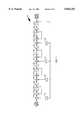
- FIG. 1An exemplary block diagram of a PLL of the prior art is shown in FIG. 1.
- a reference clockis provided by clock source 2 and provided to divider 4.
- Divider 4divides the reference clock by M to obtain a divided reference clock at the desired comparison frequency.
- VCO 10is a clock source which produces the desired clock signal.
- the clock signalis provided to divider 12 which divides the clock signal from VCO 10 by N to obtain a divided clock signal at the desired comparison frequency.
- the divided reference clock and the divided clock signalare provided to phase detector 6 which produces an error signal based on the phases of the two input signals.
- the error signalis provided to loop filter 8 which performs filtering of the error signal and provides a control voltage to VCO 10.
- the control voltageadjusts the frequency of the clock signal such that the frequency of the divided clock signal is identical to the frequency of the divided reference clock.
- the frequency of the clock signalis related to the frequency of the reference clock by the divider ratios M and N.
- the challenge in generating the clock signalis compounded by the need to generate a frequency which is fractionally related to the frequency of the reference clock.
- a receivermay need to generate various local oscillator frequencies depending on the RF frequency of the channel being received.
- the receivertypically has one clock source (e.g. VCO 10) and the frequency of the reference clock is fixed.
- the PLLcan be used to generate clock signals at various frequencies by changing the divider ratios M and/or N. In cases where the divider ratios M and/or N are not integers (fractional dividers), the phase noise of the clock signal may be degraded.
- a fractional dividercan be obtained by numerous methods.
- the clock cycle of the divided clock signalis periodically changed such that the average clock cycle of the divided clock signal is equal to the clock cycle of the divided reference clock.
- N2.5 divider
- the clock cyclecan be alternately changed between two and three cycles of the clock signal.
- the divider ratio Ncan be changed to obtain a divided clock signal at any comparison frequency lower than the frequency of the clock signal.
- the simple fractional divider as described aboveresults in a clock signal with additional phase noise.
- the varying clock cycles of the divided clock signalcause a periodic waveform to appear in the error signal at the output of phase detector 6.
- the periodic waveformis filtered by loop filter 8 but is not completely eliminated.
- the periodic waveformmanifests itself on the control voltage which causes a periodic jitter on the clock signal at the output of VCO 10.
- the periodic jittercan be observed as spurious tones above and below the frequency of the clock signal.
- the location of the spurious tonesis related to the fractional divider ratio M and/or N. More specifically, the frequency of the spurious tones is related to the periodicity of the divided reference clock and/or the divided clock signal. If the periodicity is over a many clock cycles, the error signal contains low frequency spectral components which are more difficult to filter. This results in spurious tones which are closer in frequency to the clock signal and higher in amplitude.
- the spurious tonescan degrade the performance of the application for which the clock signal is used. For example, the spurious tones can degrade the BER performance of the demodulator if the clock signal is used for demodulation of the received RF signal.
- the symbol rate and the data rateare related to the frequency of the received RF signal.
- the symbol clock and the data clockmay be derived from the clock signal.
- the data clockcan also be used to generate the output waveforms. Therefore, jitter on the clock signal manifests itself in the output waveforms and can cause objectionable distortion. If this is the case, the spurious tones can cause an audible tone to appear in the output audio signal or a visible artifact to appear in the output video signal.
- One approach to eliminating the spurious tones caused by the fractional divideris to randomize the divider ratio N such that the periodicity of the divided clock signal is eliminated.
- randomization of the divider ratioeliminates the alternating of the clock cycle between two and three cycles of the clock signal. Randomizing the clock cycle eliminates the periodicity (and thus the spurious tones) and results in a whitened error signal at the output of phase detector 6. Viewed another way, the energy in the spurious tones are evenly spread over the frequency spectrum from DC to the frequency of the clock signal.
- Loop filter 8filters the high frequency component of the error signal and results in a clock signal with improved phase noise characteristics.
- the improved phase noise resulting from the randomization of the duty cyclemay not be adequate.
- another methodis needed to further improve the phase noise of the clock signal.
- the performance of the circuitcan only benefit from any improvement in the phase noise of the clock signal.
- the present inventionis a novel and improved circuit for the generation of a clock signal having improved phase noise characteristics.
- the reference clockis divided by a variable divider to obtain a divided reference clock.
- the clock signalis divided by a second divider to obtain a divided clock signal.
- the two signalsare provided to a phase detector which generates a phase error in response to the phases of the two signals.
- the phase erroris filtered by a loop filter and the resultant control voltage is provided to a VCO.
- the VCOvaries the frequency of the clock signal in response to the control voltage.
- the reference clockis divided by a variable divider which is capable of dividing the reference clock by a divider ratio of 2, 3, 4, . . . or M depending on the value of a control signal.
- the control signalis generated from a divider controller in response to a controller input.
- the noise shaping characteristics of the divider controllerresult in selection of the variable divider ratio such that the average frequency of the divided reference clock is at the desired comparison frequency but the quantization noise from the fractional divide is pushed from low frequency to high frequency.
- the high frequency quantization noisecan be more easily filtered by subsequent filtering stages.
- the phase noise of the clock signalis improved. Additional improvements in the phase noise may be obtained by using higher order noise shapers and/or noise shapers having different frequency response characteristics.
- the divider ratios of the variable dividerare generated such that the frequency of the divided reference clock is at the desired comparison frequency.
- the value of the controller inputdetermines the divider ratio and the frequency of the divided reference clock which, in turn, determines the frequency of the clock signal.
- the divider controllercan be easily designed with many bits of resolution because of the simplicity of the noise shaper design. Thus, accurate divider ratios (and accurate frequency of the clock signal) can be simply obtained by changing the value of the controller input.
- the noise shaper designoffers great flexibility without sacrificing performance.
- the ditheringcan be derived from a random number generator or a pseudo random (PN) sequence generator.
- the random number or the PN sequencecan be filtered by a high-pass filter to remove low frequency components.
- the ditheringis provided to the noise shaper to minimize limit cycling (toggling between states) at the noise shaper output. Minimizing limit cycling removes spurious tones from the divided reference clock.
- FIG. 1is a block diagram of a phase lock loop of the prior art
- FIG. 2is a block diagram of an exemplary phase lock loop of the present invention
- FIG. 3is a block diagram of an exemplary divider controller of the present invention.
- FIG. 4is a block diagram of an exemplary noise shaper utilizing a second order single-loop delta sigma modulator
- FIG. 5is a block diagram of an exemplary noise shaper utilizing a fourth order single-loop delta sigma modulator
- FIG. 6is a block diagram of an exemplary noise shaper utilizing a fourth order feedback-network delta sigma modulator
- FIG. 7is a block diagram of an exemplary dither circuit of the present invention.
- FIG. 8is a block diagram of an exemplary variable divider of the present invention.
- FIG. 9is a diagram of the output power spectrum of the variable divider wherein the divider ratios are randomly selected.
- FIG. 10is a diagram of the output power spectrum of the variable divider wherein the divider ratios are provided a divider controller which employs a delta sigma modulator.
- Phase-locked-loopcan be used to provide a clock signal at the desired frequency based on a reference clock.
- the desired frequencycan be obtained by changing the divider ratios M and N as shown in FIG. 1.
- the PLLcan also be used to obtain the desired phase noise characteristics in the clock signal.
- the PLL loop bandwidthcan be controlled.
- the loop bandwidthdetermines the acquisition speed and the acquisition and tracking range of the PLL.
- the loop bandwidthalso determines the phase noise of the clock signal. If the reference clock has good phase noise characteristics, the loop bandwidth is typically designed to be wide to allow VCO 10 to track the reference clock. If the reference clock has poor phase noise characteristics, the loop bandwidth is typically designed to be narrow and VCO 10 may be replaced with a VCXO.
- the combination of the narrow loop bandwidth and improved phase noise from the VCXOresult in a clock signal with good phase noise characteristics. Often times, the loop bandwidth is determined based on a compromise between the desired phase noise characteristics and the acquisition and tracking requirements.
- the desired frequencycannot be obtained by selecting integer values for M and N.
- fractional dividersare used to divide the reference clock and/or the clock signal. Fractional division of the reference clock and/or clock signal can result in undesirable spurious tones appearing in the clock signal.
- the frequency of the spurious tonesis determined by the periodicity of the divided clock signal from divider 12 and/or the divided reference clock from divider 4. Longer periodicity corresponds to low frequency spurious tones in the error signal from phase detector 6. Low frequency components are more difficult to filter because of the lowpass nature of loop filter 8. The unfiltered or inadequately filtered low frequency components cause spurious tones on the clock signal.
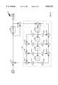
- Clock source 102generates the reference clock which is provided to variable divider 104.
- Variable divider 104divides the reference clock by 2, 3, 4, . . . or M depending on the control signal from divider controller 120.
- the output from variable divider 104, labeled as event clock,is provided to phase detector 106 and divider controller 120.
- VCO 110provides the clock signal to divider 112 which, in the exemplary embodiment, is a fixed divide by N divider.
- Divider 112can be a fractional divider, although this is neither preferred nor necessary in the present invention.
- the divided clock signal from divider 112is provided to phase detector 106.
- Phase detector 106generates an error signal based on the phases of the two input signals.
- the error signalis provided to loop filter 108 which filters the signal and provides a control voltage to VCO 110.
- the PLL of the present inventioncan be implemented in many embodiments.
- the PLLcan comprise analog or digital loop components.
- phase detector 106can be a simple phase/frequency detector implemented with two flip-flops and some logic gates in the manner well known in the art.
- Phase detector 106can also be designed for a specific application, such as an arc-tangent phase detector used for digital demodulation, and implemented with digital logic or a ROM look up table.
- Loop filter 108can be a type I, type II, or higher type loops implemented with analog components (e.g. resistors, capacitors, and an amplifier).
- Loop filter 108can also be implemented as a digital filter such as an infinite impulse response (IIR) filter.
- IIRinfinite impulse response
- Loop filter 108can have additional poles to filter undesirable high frequency components in the error signal from phase detector 106.
- the output of loop filter 108can be an analog control voltage, if VCO 110 requires an analog control signal, or a digital control value.
- VCO 110can be replaced with a VCXO or other oscillator circuits.
- VCO 110can be implemented as an NCO which requires a digital control value. The NCO can be triggered from a second independent reference clock or the same reference clock from clock source 102.
- divider 112can be implemented with simple counters or flip-flops using methods which are known in the art. The various implementations of the PLL are within the scope of the present invention.
- divider 112is implemented as a fixed integer divider. This reduces the complexity of the PLL.
- the present inventioncan be extended to include the use of a second variable divider and a second divider controller to replace divider 112.
- one set of variable divider 104 and divider controller 120is necessary to provide the desired performance.
- the present inventionis directed to the use of one or two sets of variable divider 104 and divider controller 120 to obtain the desired frequency accuracy and phase noise characteristics for the clock signal.
- divider controller 120is used to produce an event clock which has superior phase noise characteristics to an event clock generated by other methods, such as the fractional divider described above.
- the quantization noisecan be pushed from low frequency to high frequency, thus eliminating the spurious tones in the clock signal.
- the quantization noiseresults from representation of a fractional divide ratio (e.g. 8.394) with a series of integer divide ratios (e.g. 8 and 9).
- the close-in phase noise of the clock signalis improved because of the noise shaping characteristics of divider controller 120. The improved close-in phase noise minimizes degradation in the system performance.
- FIG. 3A block diagram of an exemplary divider controller 120 is shown in FIG. 3.
- the controller inputdetermines the divider ratio of variable divider 104 and thus the frequency of the clock signal.
- the controller inputcan be generated by a system controller or processor and is represented as a fine control and a coarse control in FIG. 3.
- the coarse controlcan comprise the p-1 most significant bits (MSBs) of the controller input
- the fine controlcan comprise the k-(p-1) least significant bits (LSBs) of the controller input.
- Other partitions of the controller inputscan be contemplated and are within the scope of the present invention.
- the dither output from dither circuit 140is provided to summer 142 which adds the fine control to the dither output.
- the functionality and implementation of dither circuit 140is described below.
- the output of summer 142is labeled as the noise shaper input.
- Noise shaper 150quantizes the noise shaper input and noise shapes the quantization noise.
- the noise shaper outputis provided to summer 160 which adds the coarse control to the noise shaper output.
- the output of summer 160comprises the control signal which is provided to variable divider 104.
- the coarse controlcontains the integer component of the desired divider ratio and the noise shaper output contains the fractional part.
- the coarse controlis 8 and the noise shaper output is a series of ones and zeros such that the average is 0.394. This embodiment limits the variations in the divider ratios (to 8 and 9) to minimize the error from phase detector 106.
- noise shaper 150can be implemented to accept the k-bit controller input and produce the p-bit control signal. This embodiment can result in wide variations in the divider ratios which can result in a higher error signal from phase detector 106.
- Dither circuit 140provides dithering to the divider ratios to remove spurious tones at the divided reference clock. Depending on the desired divider ratio and the implementation of noise shaper 150, dither circuit 140 may not be necessary. Therefore, the present invention is also directed to embodiments which does not employ dithering circuit 140.
- noise shaper 150is used to push the quantization noise from low frequency to higher frequency where filtering can be more easily performed.
- Noise shaper 150of many different types and of various orders can be used to perform the required noise shaping function as describe herein and are within the scope of the present invention.
- the followingis a discussion of three exemplary implementations of noise shaper 150. These implementations employ a single-loop architecture. Multi-loop architectures, such as the MASH (Multi-stAge noise SHaping) architecture, or the cascaded architecture which are known in the art, can also be utilized and are within the scope of the present invention.
- MASHMulti-stAge noise SHaping
- Noise shaper 150has the following transfer function:
- the output from noise shaper 150comprises the input signal X(z) which is shaped by the signal transfer function STF(z) plus the quantization noise E(z) which is shaped by the noise transfer function NTF(z).
- the signal transfer function STF(z)is typically designed such that it is frequency independent.
- STF(z)can be an allpass function comprising a fixed gain K and delay elements, such as K•z -2 .
- the quantization noise E(z)can be shaped by the noise transfer function NTF(z) such that the quantization noise in the band of interest (e.g. the band where the input signal is present) is pushed out-of-band where filtering is more easily performed.
- the characteristics of the noise transfer function NTF(z)is selected based on the application for which noise shaper 150 is used and is designed to provide the required performance.
- FIG. 4An exemplary noise shaper implemented with a second order single-loop delta sigma modulator 150a is shown in FIG. 4.
- the noise shaper inputis provided to summer 208 within the first section.
- the value of the noise shaper outputdetermines the fractional part of the divider ratio of variable divider 104, as described above and illustrated in FIG. 3.
- a delayed version of the noise shaper outputis also provided to summer 208a.
- Summer 208asubtracts the delayed noise shaper output from the noise shaper input and provides an error value to integrator 210a.
- summer 212aaccumulates the error value with the accumulated error value stored in register (z -1 ) 214a.
- the updated error value from summer 212ais provided to register 214a which stores the value at the next leading edge of event clock.
- the value stored in register 214arepresents an accumulation of the error values from summer 208a.
- the updated error value from summer 212ais provided to summer 208b which subtracts the delayed noise shaper output from the updated error value and provides an error value to integrator 210b.
- summer 212baccumulates the error value with the accumulated error value stored in register 214b.
- the updated error value from summer 212bis provided to register 214b which stores the value at the next leading edge of event clock.
- the updated error value from summer 212bis also provided to quantizer 218 which outputs a 1-bit value in accordance with the updated error value.
- quantizer 218retains the most significant bit from the updated error value and discards the remaining least significant bits.
- the quantized valuerepresents the noise shaper output which is provided to summer 160 (see FIG. 3).
- the quantized valueis also stored in register 220. As with register 214, register 220 is triggered off the leading edge of event clock.
- FIG. 4illustrates a second order single-loop delta sigma modulator or noise shaper.
- the transfer function of the noise shaper, from the quantization noise to the noise shaper output,can be described in the z-plane.
- the frequency responseis four, which means the amplitude of the quantization noise from noise shaper 150a is four times the amplitude of the whitened quantization noise.
- the quantization noiseis effectively pushed from low frequency to high frequency where filtering is more easily performed.
- Higher order delta sigma modulatorscan also be used to provide improved noise shaping of the quantization noise by pushing even more low frequency noise to higher frequency, thereby improving the close-in phase a noise characteristics of the clock signal.
- higher order delta sigma modulatorscan be implemented using a modified single-loop architectures.
- FIG. 5An exemplary noise shaper implemented with a fourth order single-loop delta sigma modulator 150b is shown in FIG. 5.
- the noise shaper inputis provided to summer 302a within the first section.
- the noise shaper outputis provided to gain element 310a which scales the output with the gain b 1 and provides the scaled output to summer 302a.
- Summer 302aadds the scaled output with the noise shaper input and provides an error value to the first integrator which comprises summer 304a and register 306a. Within the first integrator, summer 304a accumulates the error value from summer 302a with the accumulated error value stored in register (z -1 ) 306a.
- the error value from summer 304ais provided to register 306a which stores the value at the next leading edge of event clock (not shown in FIG. 5 for simplicity).
- the error value from register 306ais provided to gain element 308a which scales the error value with the gain a 1 .
- the scaled error value from gain element 308arepresents the output of the first section.
- the error value from gain element 308dis provided to quantizer (Q) 312 which outputs a 1-bit value in accordance with the error value.
- quantizer 218retains the most significant bits from the updated error value and discards the remaining least significant bits.
- the quantized valuerepresents the noise shaper output which is provided to summer 160 (see FIG. 3).
- the signal transfer function STF(z) and the noise transfer function NTF(z) of noise shaper 150bcan be calculated as: ##EQU1##
- the signal transfer function STF(z) and noise transfer function NTF(z)have the same poles which are given by D(z). These poles provide a gain and frequency shaping of the input signal X(z). Therefore, the c x coefficients are selected for the desired transfer function D(z). The a x and b x coefficients are then calculated based on equation (5).
- Delta sigma modulator 150bis preferred in the present invention because of its high performance and simplicity in design.
- FIG. 9illustrates the output power spectrum wherein the divider ratios are randomly selected. Notice the poor phase noise characteristic of the divided reference clock (or event clock).
- FIG. 10illustrates the output power spectrum wherein the divider ratios are provided by variable divider 104 which employs delta sigma modulator 150b. Notice the spectral purity of the divided reference clock and the improved close-in phase noise characteristics.
- the noise shaper inputcomprises 22-bits and the noise shaper output comprises 1-bit
- summers 302a, 302b, 302c, and 302dare implemented with 24-bit, 16-bit, 13-bit, and 10-bit precision, respectively
- summers 304a, 304b, 304c, and 304dare implemented with 27-bit, 19-bit, 15-bit, and 10-bit precision, respectively
- registers 306a, 306b, 306c, and 306dare implemented with 27-bit, 19-bit, 15-bit, and 10-bit precision, respectively.
- Quantizer 312outputs the MSB from register 306d.
- the numbersare represented in two's complement and a zero from quantizer 312 represents a positive value.
- a zero value from quantizer 312selects the negative values for the gains b x and a one value selects the positive values.
- noise shaper 150cAn exemplary noise shaper implemented with a fourth order feedback network is shown in FIG. 6.
- the noise shaper input and the filtered quantization noise from feedback network 410are provided to summer 402 which subtracts the filtered quantization noise from the noise shaper input.
- the resultant error valueis provided to quantizer 404 which quantizes the error value to provide the noise shaper output.
- quantizer 404outputs a 1-bit value which is the most significant bit of the error value from summer 402. More quantizer steps can also be used and are within the scope of the present invention.
- the noise shaper outputis subtracted from the error value by summer 406 to produce the quantizer error which is provided to feedback network 410.
- FIG. 6illustrates an exemplary feedback network 410 comprising a fourth order infinite impulse response (IIR) filter.
- IIRinfinite impulse response
- the IIR structureis preferred since it allows for the synthesis of both zeros and poles.
- the finite impulse response (FIR) structureallows for the synthesis of only poles but no zeros.
- the quantizer error from summer 406 and the feedback value from summer 420dare provide to summer 422 which subtracts the feedback value from the quantizer error.
- the summed value from summer 422is stored in delay element 416d.
- Delay elements 416a, 416b, 416c, and 416dare connected in a cascade configuration (as shown in FIG. 6) and are clocked by the event clock (not shown in FIG. 6).
- the outputs from delay elements 416are provided to gain elements 418 which scale the outputs with the corresponding gains D.
- the scaled value from gain elements 418are accumulated by summers 420 and the accumulated value is provided to summer 422.
- the outputs from delay elements 416are also provided to gain elements 414 which scales the outputs with the corresponding gains C.
- the scaled values from gain elements 414are accumulated by summers 412 and the accumulated values are the output of feedback network 410.
- the transfer function of feedback network 410can be expressed as: ##EQU2##
- the noise transfer function NTF(z) of the quantization noise from quantizer 404 to the noise shaper outputcan be calculated to be 1+H f (z) or: ##EQU3##
- noise shaper 150cprovides for four zeros and four poles.
- the placement of the pole locationcan be controlled by proper selection of the gains D within feedback network 410.
- the placement of the zero locationcan be controlled by proper selection of the gains C, assuming the gains D have been fixed.
- the placement of the zero and pole locationdirectly affect the noise shaping of the quantizer error and, thus, the phase noise characteristics.
- the present inventionis directed at the use of any combination of gains C and D which produce the desired noise shaping response.
- dither circuit 140provides dithering of the noise shaper input to minimize limit cycling at the output of noise shaper 150.
- Limit cyclingresults from noise shaper 150 not having the resolution to produce the desired output value and having to periodically toggle between states or periodically traverse through a series of states. The periodicity causes spurious tones to appear at the divided reference clock from variable divider 104.
- a small random or pseudo random valueis added to the noise shaper input. The amount of dithering is selected to be small enough to minimize degradation in the performance of the system.
- the ditheringis high-pass filtered to remove low frequency components which can degrade the phase noise characteristics of the clock signal.
- Dither circuit 140contains pseudo random (PN) generator 510 and high-pass filter 520.
- PNpseudo random
- high-pass filter 520may not be necessary since only a small amount of dither is added to the noise shaper input.
- the present inventionis directed at the use of dither circuit 140 with and without high-pass filter 520.
- PN generator 510is implemented with plurality of delay elements 512 and modulo-2 adders 514.
- Delay elements 512are connected in a cascade configuration and are clocked with the event clock (not shown in FIG. 7).
- Modulo-2 adders 514are interposed between successive delay elements 512 at the proper locations determined by the PN polynomial.
- the PN output from delay element 512ois also provided to modulo-2 adders 514.
- Delay elements 512can be implemented with registers or flip-flops as is known in the art.
- FIG. 7illustrates an exemplary PN generator 510 which implements the PN sequence of length 2 15 -1 and is defined by the polynomial:
- PN sequences of different lengthscan also be implemented. Furthermore, for a given length, it may be possible to utilize different polynomials.
- the present inventionis directed at the use of PN sequence of any length and implemented by any polynomial.
- the PN outputis high-pass filtered to remove low frequency noise components.
- An exemplary high-pass filter implemented as a fourth order FIR filteris shown in FIG. 7.
- High-pass filter 520comprises a plurality of delay elements 522 connected in cascade and clocked with the event clock (not shown in FIG. 7).
- the PN output and the outputs from delay elements 522are provided to gain elements 524 which scale the outputs with the corresponding gains G.
- the scaled value from gain elements 524are accumulated by summers 526 and the accumulated value is the dither output from high-pass filter 520.
- High-pass filter 520can be implemented with more or less taps to provide the desired filter response. High-pass filter 520 can also be implemented with other filter structures, such as an IIR filter. Different implementations of high-pass filter 520 are within the scope of the present invention.
- variable divider 104divides the reference clock by 2, 3, 4 . . . or M depending on the control signal from divider controller 120.
- the control signalcomprises p bits where p ⁇ log 2 (M-1).
- the control signalis based on the value of the controller input which comprises k bits.
- the present inventionis directed at the use of any number of bits for k and p.
- Counter 602is a simple p-bit up counter with a synchronous load input. This type of counter is known in the art. Counter 602 increments the output by one on every cycle of the reference clock. Counter 602 loads the output with the load value it receives a high load pulse at the LOAD input. The load is synchronous and the counter output only changes on the leading edge of the reference clock.
- the output of counter 602is provided to comparator 604.
- Comparator 604compares the counter output with the control signal and outputs a high load pulse when the values of the two signals are equal.
- the load pulse from comparator 604is provided to D flip-flop 606 which clocks the load pulse with the reference clock to provide the event clock.
- Flip-flop 606provides a clean pulse and aligns the event clock with the reference clock to ensure proper timing in subsequent circuits.
- the load pulseis also provided to counter 602. The load pulse loads the output of counter 602 with the load value at the next leading edge of the reference clock.
- variable divider 104outputs one pulse which is one reference clock cycle wide for every x clock cycles of the reference clock where x is the value of the control signal (counter 602 starts at one and counts to x).
- Variable divider 104can be implemented by other embodiments which are within the scope of the present invention.
Landscapes
- Stabilization Of Oscillater, Synchronisation, Frequency Synthesizers (AREA)
Abstract
Description
1. Field of the Invention
The present invention relates to electronics circuits. More particularly, the present invention relates to a novel and improved phase-locked-loop (PLL) which employs a noise shaper for generating a sinusoid having improved phase noise.
2. Description of the Related Art
Phase-locked-loops (PLLs) are an integral part of many electronic circuits and are particularly important in communication circuits. In most digital circuits, clock signals are needed to trigger the synchronous devices. In communication systems, clock signals from local oscillators (LOs) are needed for frequency conversion of the received and transmitted RF signals. Clock signals can be generated from a variety of sources such as voltage-controlled-oscillators (VCO), voltage-controlled-crystal-oscillators (VCXO), temperature-compensated-crystal-oscillators (TCXO), numerically-controlled-oscillators (NCO), multivibrators, or other types of oscillators. Depending on the source of the clock signals and the frequency, accuracy, and phase noise requirements, the clock signals derived from these sources may or may not meet the required specifications. For example, a VCO has a wide frequency control range, poor frequency accuracy, and poor phase noise characteristics. A VCXO has a narrow frequency control range but high frequency accuracy and good phase noise characteristics. PLLs are employed to provide frequency accuracy and improved phase noise.
The requirements of the clock signals are typically determined by the application for which the clock signals are used. An application which is especially critical of the requirements of the clock signals is digital communication. For demodulation of a digitally modulated waveform using binary-phase-shift-keying (BPSK), quadrature-phase-shift-keying (QPSK), offset QPSK (OQPSK), m-ary phase-shift-keying (PSK), or quadrature amplitude modulation (QAM) it may be necessary for the system to lock to the received RF signal. The performance of the demodulator, as indicated by the degradation in the measured bit error rate (BER) versus the theoretical BER, is influenced by the phase noise of the generated clock signals. The phase noise is spectrally related to the jitter on the clock signal. PLLs are used to generate clock signals at the precise frequency and with the required phase noise characteristics.
An exemplary block diagram of a PLL of the prior art is shown in FIG. 1. A reference clock is provided by clock source 2 and provided to divider 4.Divider 4 divides the reference clock by M to obtain a divided reference clock at the desired comparison frequency. VCO 10 is a clock source which produces the desired clock signal. The clock signal is provided to divider 12 which divides the clock signal fromVCO 10 by N to obtain a divided clock signal at the desired comparison frequency. The divided reference clock and the divided clock signal are provided to phase detector 6 which produces an error signal based on the phases of the two input signals. The error signal is provided to loopfilter 8 which performs filtering of the error signal and provides a control voltage toVCO 10. The control voltage adjusts the frequency of the clock signal such that the frequency of the divided clock signal is identical to the frequency of the divided reference clock. The frequency of the clock signal is related to the frequency of the reference clock by the divider ratios M and N.
The challenge in generating the clock signal is compounded by the need to generate a frequency which is fractionally related to the frequency of the reference clock. As an exemplary application where this is necessary, a receiver may need to generate various local oscillator frequencies depending on the RF frequency of the channel being received. The receiver typically has one clock source (e.g. VCO 10) and the frequency of the reference clock is fixed. The PLL can be used to generate clock signals at various frequencies by changing the divider ratios M and/or N. In cases where the divider ratios M and/or N are not integers (fractional dividers), the phase noise of the clock signal may be degraded.
A fractional divider can be obtained by numerous methods. In the simplest method, the clock cycle of the divided clock signal is periodically changed such that the average clock cycle of the divided clock signal is equal to the clock cycle of the divided reference clock. For example, to obtain an N=2.5 divider, the clock cycle can be alternately changed between two and three cycles of the clock signal. In theory, the divider ratio N can be changed to obtain a divided clock signal at any comparison frequency lower than the frequency of the clock signal.
The simple fractional divider as described above results in a clock signal with additional phase noise. The varying clock cycles of the divided clock signal cause a periodic waveform to appear in the error signal at the output of phase detector 6. The periodic waveform is filtered byloop filter 8 but is not completely eliminated. The periodic waveform manifests itself on the control voltage which causes a periodic jitter on the clock signal at the output ofVCO 10. In the frequency domain, the periodic jitter can be observed as spurious tones above and below the frequency of the clock signal. The location of the spurious tones is related to the fractional divider ratio M and/or N. More specifically, the frequency of the spurious tones is related to the periodicity of the divided reference clock and/or the divided clock signal. If the periodicity is over a many clock cycles, the error signal contains low frequency spectral components which are more difficult to filter. This results in spurious tones which are closer in frequency to the clock signal and higher in amplitude.
The spurious tones can degrade the performance of the application for which the clock signal is used. For example, the spurious tones can degrade the BER performance of the demodulator if the clock signal is used for demodulation of the received RF signal. In many communication systems, the symbol rate and the data rate are related to the frequency of the received RF signal. Thus, the symbol clock and the data clock may be derived from the clock signal. The data clock can also be used to generate the output waveforms. Therefore, jitter on the clock signal manifests itself in the output waveforms and can cause objectionable distortion. If this is the case, the spurious tones can cause an audible tone to appear in the output audio signal or a visible artifact to appear in the output video signal.
One approach to eliminating the spurious tones caused by the fractional divider is to randomize the divider ratio N such that the periodicity of the divided clock signal is eliminated. For the divide by 2.5 example given above, randomization of the divider ratio eliminates the alternating of the clock cycle between two and three cycles of the clock signal. Randomizing the clock cycle eliminates the periodicity (and thus the spurious tones) and results in a whitened error signal at the output of phase detector 6. Viewed another way, the energy in the spurious tones are evenly spread over the frequency spectrum from DC to the frequency of the clock signal.Loop filter 8 filters the high frequency component of the error signal and results in a clock signal with improved phase noise characteristics.
In some applications, the improved phase noise resulting from the randomization of the duty cycle may not be adequate. When this occurs, another method is needed to further improve the phase noise of the clock signal. For all applications, the performance of the circuit can only benefit from any improvement in the phase noise of the clock signal.
The present invention is a novel and improved circuit for the generation of a clock signal having improved phase noise characteristics. In accordance with the present invention, the reference clock is divided by a variable divider to obtain a divided reference clock. The clock signal is divided by a second divider to obtain a divided clock signal. The two signals are provided to a phase detector which generates a phase error in response to the phases of the two signals. The phase error is filtered by a loop filter and the resultant control voltage is provided to a VCO. The VCO varies the frequency of the clock signal in response to the control voltage.
It is an object of the present invention to provide a clock signal with improved phase noise characteristics. The reference clock is divided by a variable divider which is capable of dividing the reference clock by a divider ratio of 2, 3, 4, . . . or M depending on the value of a control signal. The control signal is generated from a divider controller in response to a controller input. The noise shaping characteristics of the divider controller result in selection of the variable divider ratio such that the average frequency of the divided reference clock is at the desired comparison frequency but the quantization noise from the fractional divide is pushed from low frequency to high frequency. The high frequency quantization noise can be more easily filtered by subsequent filtering stages. By pushing the quantization noise to higher frequency, the phase noise of the clock signal is improved. Additional improvements in the phase noise may be obtained by using higher order noise shapers and/or noise shapers having different frequency response characteristics.
It is another object of the present invention to obtain a clock signal having a wide frequency control range and high frequency accuracy. The divider ratios of the variable divider are generated such that the frequency of the divided reference clock is at the desired comparison frequency. The value of the controller input determines the divider ratio and the frequency of the divided reference clock which, in turn, determines the frequency of the clock signal. The divider controller can be easily designed with many bits of resolution because of the simplicity of the noise shaper design. Thus, accurate divider ratios (and accurate frequency of the clock signal) can be simply obtained by changing the value of the controller input. The noise shaper design offers great flexibility without sacrificing performance.
It is yet another object of the present invention to provide dithering to the divider ratios of the variable divider. The dithering can be derived from a random number generator or a pseudo random (PN) sequence generator. The random number or the PN sequence can be filtered by a high-pass filter to remove low frequency components. The dithering is provided to the noise shaper to minimize limit cycling (toggling between states) at the noise shaper output. Minimizing limit cycling removes spurious tones from the divided reference clock.
The features, objects, and advantages of the present invention will become more apparent from the detailed description set forth below when taken in conjunction with the drawings in which like reference characters identify correspondingly throughout and wherein:
FIG. 1 is a block diagram of a phase lock loop of the prior art;
FIG. 2 is a block diagram of an exemplary phase lock loop of the present invention;
FIG. 3 is a block diagram of an exemplary divider controller of the present invention;
FIG. 4 is a block diagram of an exemplary noise shaper utilizing a second order single-loop delta sigma modulator;
FIG. 5 is a block diagram of an exemplary noise shaper utilizing a fourth order single-loop delta sigma modulator;
FIG. 6 is a block diagram of an exemplary noise shaper utilizing a fourth order feedback-network delta sigma modulator;
FIG. 7 is a block diagram of an exemplary dither circuit of the present invention;
FIG. 8 is a block diagram of an exemplary variable divider of the present invention;
FIG. 9 is a diagram of the output power spectrum of the variable divider wherein the divider ratios are randomly selected; and
FIG. 10 is a diagram of the output power spectrum of the variable divider wherein the divider ratios are provided a divider controller which employs a delta sigma modulator.
Phase-locked-loop (PLL) can be used to provide a clock signal at the desired frequency based on a reference clock. The desired frequency can be obtained by changing the divider ratios M and N as shown in FIG. 1. The PLL can also be used to obtain the desired phase noise characteristics in the clock signal. By proper design ofloop filter 8, the PLL loop bandwidth can be controlled. The loop bandwidth determines the acquisition speed and the acquisition and tracking range of the PLL. The loop bandwidth also determines the phase noise of the clock signal. If the reference clock has good phase noise characteristics, the loop bandwidth is typically designed to be wide to allowVCO 10 to track the reference clock. If the reference clock has poor phase noise characteristics, the loop bandwidth is typically designed to be narrow andVCO 10 may be replaced with a VCXO. The combination of the narrow loop bandwidth and improved phase noise from the VCXO result in a clock signal with good phase noise characteristics. Often times, the loop bandwidth is determined based on a compromise between the desired phase noise characteristics and the acquisition and tracking requirements.
In many applications, the desired frequency cannot be obtained by selecting integer values for M and N. When this occurs, fractional dividers are used to divide the reference clock and/or the clock signal. Fractional division of the reference clock and/or clock signal can result in undesirable spurious tones appearing in the clock signal. The frequency of the spurious tones is determined by the periodicity of the divided clock signal fromdivider 12 and/or the divided reference clock fromdivider 4. Longer periodicity corresponds to low frequency spurious tones in the error signal from phase detector 6. Low frequency components are more difficult to filter because of the lowpass nature ofloop filter 8. The unfiltered or inadequately filtered low frequency components cause spurious tones on the clock signal. Some applications are especially sensitive to spurious tones which are close to the frequency of the clock signal since these spurious tones can cause objectionable degradation in the output signals (e.g. output audio and video signals).
A block diagram of the PLL of the present invention is shown in FIG. 2.Clock source 102 generates the reference clock which is provided tovariable divider 104.Variable divider 104 divides the reference clock by 2, 3, 4, . . . or M depending on the control signal fromdivider controller 120. The output fromvariable divider 104, labeled as event clock, is provided tophase detector 106 anddivider controller 120. Within the PLL,VCO 110 provides the clock signal to divider 112 which, in the exemplary embodiment, is a fixed divide by N divider.Divider 112 can be a fractional divider, although this is neither preferred nor necessary in the present invention. The divided clock signal fromdivider 112 is provided tophase detector 106.Phase detector 106 generates an error signal based on the phases of the two input signals. The error signal is provided toloop filter 108 which filters the signal and provides a control voltage toVCO 110.
The PLL of the present invention can be implemented in many embodiments. The PLL can comprise analog or digital loop components. For example,phase detector 106 can be a simple phase/frequency detector implemented with two flip-flops and some logic gates in the manner well known in the art.Phase detector 106 can also be designed for a specific application, such as an arc-tangent phase detector used for digital demodulation, and implemented with digital logic or a ROM look up table.Loop filter 108 can be a type I, type II, or higher type loops implemented with analog components (e.g. resistors, capacitors, and an amplifier).Loop filter 108 can also be implemented as a digital filter such as an infinite impulse response (IIR) filter.Loop filter 108 can have additional poles to filter undesirable high frequency components in the error signal fromphase detector 106. The output ofloop filter 108 can be an analog control voltage, ifVCO 110 requires an analog control signal, or a digital control value.VCO 110 can be replaced with a VCXO or other oscillator circuits.VCO 110 can be implemented as an NCO which requires a digital control value. The NCO can be triggered from a second independent reference clock or the same reference clock fromclock source 102. Finally,divider 112 can be implemented with simple counters or flip-flops using methods which are known in the art. The various implementations of the PLL are within the scope of the present invention.
In the preferred embodiment,divider 112 is implemented as a fixed integer divider. This reduces the complexity of the PLL. However, the present invention can be extended to include the use of a second variable divider and a second divider controller to replacedivider 112. Furthermore, it is possible to swapvariable divider 104 anddivider controller 120 withdivider 112. Typically, one set ofvariable divider 104 anddivider controller 120 is necessary to provide the desired performance. However, the present invention is directed to the use of one or two sets ofvariable divider 104 anddivider controller 120 to obtain the desired frequency accuracy and phase noise characteristics for the clock signal.
Divider Controller
In the present invention,divider controller 120 is used to produce an event clock which has superior phase noise characteristics to an event clock generated by other methods, such as the fractional divider described above. By controlling the clock cycle of the event clock in an non-periodic manner (or periodic over a very long period) the quantization noise can be pushed from low frequency to high frequency, thus eliminating the spurious tones in the clock signal. The quantization noise results from representation of a fractional divide ratio (e.g. 8.394) with a series of integer divide ratios (e.g. 8 and 9). Furthermore, the close-in phase noise of the clock signal (phase noise close to the frequency of the clock signal) is improved because of the noise shaping characteristics ofdivider controller 120. The improved close-in phase noise minimizes degradation in the system performance.
A block diagram of anexemplary divider controller 120 is shown in FIG. 3. The controller input (see FIG. 2) determines the divider ratio ofvariable divider 104 and thus the frequency of the clock signal. The controller input can be generated by a system controller or processor and is represented as a fine control and a coarse control in FIG. 3. For example, if the controller input contains k-bits and the control signal contains p-bits, the coarse control can comprise the p-1 most significant bits (MSBs) of the controller input and the fine control can comprise the k-(p-1) least significant bits (LSBs) of the controller input. Other partitions of the controller inputs can be contemplated and are within the scope of the present invention.
Withindivider controller 120, the dither output fromdither circuit 140 is provided tosummer 142 which adds the fine control to the dither output. The functionality and implementation ofdither circuit 140 is described below. The output ofsummer 142 is labeled as the noise shaper input.Noise shaper 150 quantizes the noise shaper input and noise shapes the quantization noise. The noise shaper output is provided to summer 160 which adds the coarse control to the noise shaper output. The output of summer 160 comprises the control signal which is provided tovariable divider 104.
In the exemplary embodiment, the coarse control contains the integer component of the desired divider ratio and the noise shaper output contains the fractional part. For the divide by 8.394 example given above, the coarse control is 8 and the noise shaper output is a series of ones and zeros such that the average is 0.394. This embodiment limits the variations in the divider ratios (to 8 and 9) to minimize the error fromphase detector 106.
Other embodiments ofdivider controller 120 can be designed. For example,noise shaper 150 can be implemented to accept the k-bit controller input and produce the p-bit control signal. This embodiment can result in wide variations in the divider ratios which can result in a higher error signal fromphase detector 106.
Noise Shaper
In the present invention,noise shaper 150 is used to push the quantization noise from low frequency to higher frequency where filtering can be more easily performed.Noise shaper 150 of many different types and of various orders can be used to perform the required noise shaping function as describe herein and are within the scope of the present invention. The following is a discussion of three exemplary implementations ofnoise shaper 150. These implementations employ a single-loop architecture. Multi-loop architectures, such as the MASH (Multi-stAge noise SHaping) architecture, or the cascaded architecture which are known in the art, can also be utilized and are within the scope of the present invention.
Y(z)=STF(z)X(z)+NTF(z)E(z), (1)
where Y(z) is the output from noise shaper 150 in the z-transform domain, X(z) is the input tonoise shaper 150, STF(z) is the signal transfer function from the input to the output ofnoise shaper 150, E(z) is the quantization noise, and NTF(z) is the noise transfer function from the quantizer to the output ofnoise shaper 150. Thus, the output fromnoise shaper 150 comprises the input signal X(z) which is shaped by the signal transfer function STF(z) plus the quantization noise E(z) which is shaped by the noise transfer function NTF(z). To avoid distortion of the input signal X(z), the signal transfer function STF(z) is typically designed such that it is frequency independent. For example, STF(z) can be an allpass function comprising a fixed gain K and delay elements, such as K•z-2. The quantization noise E(z) can be shaped by the noise transfer function NTF(z) such that the quantization noise in the band of interest (e.g. the band where the input signal is present) is pushed out-of-band where filtering is more easily performed. The characteristics of the noise transfer function NTF(z) is selected based on the application for whichnoise shaper 150 is used and is designed to provide the required performance.
An exemplary noise shaper implemented with a second order single-loopdelta sigma modulator 150a is shown in FIG. 4. The noise shaper input is provided to summer 208 within the first section. The value of the noise shaper output determines the fractional part of the divider ratio ofvariable divider 104, as described above and illustrated in FIG. 3. A delayed version of the noise shaper output is also provided tosummer 208a.Summer 208a subtracts the delayed noise shaper output from the noise shaper input and provides an error value tointegrator 210a. Withinintegrator 210a,summer 212a accumulates the error value with the accumulated error value stored in register (z-1) 214a. The updated error value fromsummer 212a is provided to register 214a which stores the value at the next leading edge of event clock. The value stored inregister 214a represents an accumulation of the error values fromsummer 208a.
The updated error value fromsummer 212a is provided tosummer 208b which subtracts the delayed noise shaper output from the updated error value and provides an error value tointegrator 210b. Withinintegrator 210b,summer 212b accumulates the error value with the accumulated error value stored inregister 214b. The updated error value fromsummer 212b is provided to register 214b which stores the value at the next leading edge of event clock.
The updated error value fromsummer 212b is also provided toquantizer 218 which outputs a 1-bit value in accordance with the updated error value. In the exemplary embodiment,quantizer 218 retains the most significant bit from the updated error value and discards the remaining least significant bits. The quantized value represents the noise shaper output which is provided to summer 160 (see FIG. 3). The quantized value is also stored inregister 220. As with register 214, register 220 is triggered off the leading edge of event clock.
FIG. 4 illustrates a second order single-loop delta sigma modulator or noise shaper. The transfer function of the noise shaper, from the quantization noise to the noise shaper output, can be described in the z-plane. For the second order noise shaper shown in FIG. 4, the transfer function can be described by two poles at z=0 and two zeros at z=+1. At low frequency, the zero dominates and the amplitude of the frequency response is small. At fs/6, where fs is the sampling rate or the frequency at which registers 214 and 220 are triggered, the response is unity. At this frequency, the amount of quantization noise fromnoise shaper 150a is the same as if the quantization noise was whitened. And at fs/2, the frequency response is four, which means the amplitude of the quantization noise fromnoise shaper 150a is four times the amplitude of the whitened quantization noise. Thus, the quantization noise is effectively pushed from low frequency to high frequency where filtering is more easily performed.
Higher order delta sigma modulators can also be used to provide improved noise shaping of the quantization noise by pushing even more low frequency noise to higher frequency, thereby improving the close-in phase a noise characteristics of the clock signal. In practice, it is difficult to design higher order delta sigma modulator using the structure shown in FIG. 4 because of concern over instability. However, higher order single-loop delta sigma modulators can be implemented using a modified single-loop architectures.
An exemplary noise shaper implemented with a fourth order single-loopdelta sigma modulator 150b is shown in FIG. 5. The noise shaper input is provided tosummer 302a within the first section. The noise shaper output is provided to gainelement 310a which scales the output with the gain b1 and provides the scaled output tosummer 302a.Summer 302a adds the scaled output with the noise shaper input and provides an error value to the first integrator which comprisessummer 304a and register 306a. Within the first integrator,summer 304a accumulates the error value fromsummer 302a with the accumulated error value stored in register (z-1) 306a. The error value fromsummer 304a is provided to register 306a which stores the value at the next leading edge of event clock (not shown in FIG. 5 for simplicity). The error value fromregister 306a is provided to gainelement 308a which scales the error value with the gain a1. The scaled error value fromgain element 308a represents the output of the first section.
The subsequent three sections are connected in the same manner as the first section. However, in the fourth section, the error value from gain element 308d is provided to quantizer (Q) 312 which outputs a 1-bit value in accordance with the error value. In the exemplary embodiment,quantizer 218 retains the most significant bits from the updated error value and discards the remaining least significant bits. The quantized value represents the noise shaper output which is provided to summer 160 (see FIG. 3). The signal transfer function STF(z) and the noise transfer function NTF(z) ofnoise shaper 150b can be calculated as: ##EQU1## where
D(z)=z.sup.4 +z.sup.3 (-4-c.sub.4)+z.sup.2 (6-c.sub.3 +3c.sub.4)+z.sup.1 (-4-c.sub.2 +2c.sub.3 -3c.sub.4)+(1-c.sub.1 +c.sub.2 -c.sub.3 +c.sub.4)(4)
and
c.sub.1 =b.sub.1 •a.sub.1 •a.sub.2 •a.sub.3 •a.sub.4, c.sub.2 =b.sub.2 •a.sub.2 •a.sub.3 •a.sub.4, c.sub.3 =b.sub.3 •a.sub.3 •a.sub.4, c.sub.4 =b.sub.4 •a.sub.4. (5)
From equation (2), the noise transfer function NTF(z) has four zeros at z=1. The signal transfer function STF(z) and noise transfer function NTF(z) have the same poles which are given by D(z). These poles provide a gain and frequency shaping of the input signal X(z). Therefore, the cx coefficients are selected for the desired transfer function D(z). The ax and bx coefficients are then calculated based on equation (5).
The details of an exemplary implementation ofdelta sigma modulator 150b which provides the performance illustrated in FIG. 10 are given below. In the exemplary embodiment, the noise shaper input comprises 22-bits and the noise shaper output comprises 1-bit,summers 302a, 302b, 302c, and 302d are implemented with 24-bit, 16-bit, 13-bit, and 10-bit precision, respectively,summers 304a, 304b, 304c, and 304d are implemented with 27-bit, 19-bit, 15-bit, and 10-bit precision, respectively, registers 306a, 306b, 306c, and 306d are implemented with 27-bit, 19-bit, 15-bit, and 10-bit precision, respectively. In the exemplary embodiment, the gains a1 =2-12, a2 =2-7, a3 =2-6, and a4 =1 can be implemented by retaining the appropriate number of MSBs and discarding the remaining LSBs and the gains b1 ±3,294,293, b2 ±11,518, b3 ±603, and b4 ±35 can be implemented by hardwired values. Quantizer 312 outputs the MSB from register 306d. In the exemplary implementation, the numbers are represented in two's complement and a zero from quantizer 312 represents a positive value. A zero value from quantizer 312 selects the negative values for the gains bx and a one value selects the positive values.
An exemplary noise shaper implemented with a fourth order feedback network is shown in FIG. 6. Withinnoise shaper 150c, the noise shaper input and the filtered quantization noise fromfeedback network 410 are provided tosummer 402 which subtracts the filtered quantization noise from the noise shaper input. The resultant error value is provided to quantizer 404 which quantizes the error value to provide the noise shaper output. In the exemplary embodiment, quantizer 404 outputs a 1-bit value which is the most significant bit of the error value fromsummer 402. More quantizer steps can also be used and are within the scope of the present invention. The noise shaper output is subtracted from the error value bysummer 406 to produce the quantizer error which is provided tofeedback network 410.
FIG. 6 illustrates anexemplary feedback network 410 comprising a fourth order infinite impulse response (IIR) filter. The IIR structure is preferred since it allows for the synthesis of both zeros and poles. The finite impulse response (FIR) structure allows for the synthesis of only poles but no zeros. The quantizer error fromsummer 406 and the feedback value fromsummer 420d are provide tosummer 422 which subtracts the feedback value from the quantizer error. The summed value fromsummer 422 is stored indelay element 416d. Delayelements summer 422. The outputs from delay elements 416 are also provided to gain elements 414 which scales the outputs with the corresponding gains C. The scaled values from gain elements 414 are accumulated by summers 412 and the accumulated values are the output offeedback network 410. The transfer function offeedback network 410 can be expressed as: ##EQU2##
The noise transfer function NTF(z) of the quantization noise from quantizer 404 to the noise shaper output can be calculated to be 1+Hf (z) or: ##EQU3##
As shown in equation (7),noise shaper 150c provides for four zeros and four poles. The placement of the pole location can be controlled by proper selection of the gains D withinfeedback network 410. The placement of the zero location can be controlled by proper selection of the gains C, assuming the gains D have been fixed. The placement of the zero and pole location directly affect the noise shaping of the quantizer error and, thus, the phase noise characteristics. The present invention is directed at the use of any combination of gains C and D which produce the desired noise shaping response.
Dither Circuit
In the present invention,dither circuit 140 provides dithering of the noise shaper input to minimize limit cycling at the output ofnoise shaper 150. Limit cycling results fromnoise shaper 150 not having the resolution to produce the desired output value and having to periodically toggle between states or periodically traverse through a series of states. The periodicity causes spurious tones to appear at the divided reference clock fromvariable divider 104. To minimize the effect of limit cycling, a small random or pseudo random value is added to the noise shaper input. The amount of dithering is selected to be small enough to minimize degradation in the performance of the system. Furthermore, in the exemplary embodiment, the dithering is high-pass filtered to remove low frequency components which can degrade the phase noise characteristics of the clock signal.
A block diagram illustrating an exemplary dither circuit is shown in FIG. 7.Dither circuit 140 contains pseudo random (PN)generator 510 and high-pass filter 520. In some applications, high-pass filter 520 may not be necessary since only a small amount of dither is added to the noise shaper input. The present invention is directed at the use ofdither circuit 140 with and without high-pass filter 520.
FIG. 7 illustrates anexemplary PN generator 510 which implements the PN sequence of length 215 -1 and is defined by the polynomial:
P(x)=x.sup.15 +x.sup.13 +x.sup.9 +x.sup.8 +x.sup.7 +x.sup.5 +1,(8)
Other PN sequences of different lengths can also be implemented. Furthermore, for a given length, it may be possible to utilize different polynomials. The present invention is directed at the use of PN sequence of any length and implemented by any polynomial.
In the exemplary embodiment, the PN output is high-pass filtered to remove low frequency noise components. An exemplary high-pass filter implemented as a fourth order FIR filter is shown in FIG. 7. High-pass filter 520 comprises a plurality of delay elements 522 connected in cascade and clocked with the event clock (not shown in FIG. 7). The PN output and the outputs from delay elements 522 are provided to gain elements 524 which scale the outputs with the corresponding gains G. In the exemplary embodiment, the gains are G4 =1, G3 =-3, G2 =3, G1 =-1. The scaled value from gain elements 524 are accumulated bysummers 526 and the accumulated value is the dither output from high-pass filter 520.
High-pass filter 520 can be implemented with more or less taps to provide the desired filter response. High-pass filter 520 can also be implemented with other filter structures, such as an IIR filter. Different implementations of high-pass filter 520 are within the scope of the present invention.
Variable Divider
In the present invention,variable divider 104 divides the reference clock by 2, 3, 4 . . . or M depending on the control signal fromdivider controller 120. The control signal comprises p bits where p≧log2 (M-1). The control signal is based on the value of the controller input which comprises k bits. The value of the controller input determines the average cycle width of the event clock and the frequency of the clock signal. Therefore, a greater number of bits for the controller input (greater value for k) allows for greater accuracy in setting the frequency of the clock signal. For example, k=20 bits allows for better than one part per million resolution in setting the frequency of the clock signal. The present invention is directed at the use of any number of bits for k and p.
A block diagram of an exemplaryvariable divider 104 is shown in FIG. 8.Counter 602 is a simple p-bit up counter with a synchronous load input. This type of counter is known in the art.Counter 602 increments the output by one on every cycle of the reference clock. Counter 602 loads the output with the load value it receives a high load pulse at the LOAD input. The load is synchronous and the counter output only changes on the leading edge of the reference clock.
The output ofcounter 602 is provided tocomparator 604.Comparator 604 compares the counter output with the control signal and outputs a high load pulse when the values of the two signals are equal. The load pulse fromcomparator 604 is provided to D flip-flop 606 which clocks the load pulse with the reference clock to provide the event clock. Flip-flop 606 provides a clean pulse and aligns the event clock with the reference clock to ensure proper timing in subsequent circuits. The load pulse is also provided to counter 602. The load pulse loads the output ofcounter 602 with the load value at the next leading edge of the reference clock. If the load value is one,variable divider 104 outputs one pulse which is one reference clock cycle wide for every x clock cycles of the reference clock where x is the value of the control signal (counter 602 starts at one and counts to x).Variable divider 104 can be implemented by other embodiments which are within the scope of the present invention.
The previous description of the preferred embodiments is provided to enable any person skilled in the art to make or use the present invention. The various modifications to these embodiments will be readily apparent to those skilled in the art, and the generic principles defined herein may be applied to other embodiments without the use of the inventive faculty. Thus, the present invention is not intended to be limited to the embodiments shown herein but is to be accorded the widest scope consistent with the principles and novel features disclosed herein.
Claims (20)
1. A circuit for providing an event clock having improved phase noise characteristics comprising:
a divider controller having an input for receiving an input value and an output, said divider controller producing a control signal at said output in response to said input value; and
a variable divider having an divider input for receiving a reference clock, a control input connected to said output of said divider controller, and an output, said variable divider producing said event clock at said output having cycle widths in response to said control signal.
2. The circuit of claim 1 wherein said divider controller comprises a noise shaper, said noise shaper having and input for receiving said input value and an output; and
wherein said control signal is dependent on said output of said noise shaper.
3. The circuit of claim 2 wherein said divider controller further comprises a dither circuit, said dither circuit having and output to said input of said noise shaper.
4. The circuit of claim 3 wherein said dither circuit comprises a PN generator having an output, wherein said output of said PN generator is said output of said dither circuit.
5. The circuit of claim 1 wherein said variable divider divides said reference clock by M where M is an integer which is dependent on said control signal.
6. A phase lock loop circuit for providing a clock signal having improved phase noise characteristics comprising:
a divider controller having an input for receiving an input value and an output, said divider controller producing a control signal at said output in response to said input value; and
a variable divider having an divider input for receiving a reference clock, a control input connected to said output of said divider controller, and an output, said variable divider producing said event clock at said output having cycle widths in response to said control signal;
an oscillator having an input and an output, said oscillator producing a clock signal at said output, said clock signal having a frequency which is responsive to said input;
a divider having an input connected to said output of said oscillator and an output, said divider dividing said clock signal
a phase detector having two inputs and an output, one input connected to said output of said variable divider and another input connected to said output of said divider; and
a loop filter having an input connected to said output of said phase detector and an output connected to said input of said oscillator.
7. The circuit of claim 6 wherein said divider controller comprises a noise shaper, said noise shaper having and input for receiving said input value and an output; and
wherein said control signal is dependent on said output of said noise shaper.
8. The circuit of claim 6 wherein said divider is a fixed N divider, where N is an integer.
9. An apparatus for providing an event clock having improved phase noise characteristics comprising:
noise shaping means for receiving a controller input and providing a control signal in response to said controller input; and
variable divider means for receiving a reference clock and said control signal, said variable divider means dividing said reference clock by a divide ratio corresponding to a value of said control signal.
10. The apparatus of claim 9 wherein said noise shaping means comprises a second order noise shaper.
11. The apparatus of claim 9 wherein said noise shaping means comprises a fourth order noise shaper.
12. The apparatus of claim 9 wherein said variable divider means divides said reference clock by M where M is an integer which is dependent on said value of said control signal.
13. The apparatus of claim 9 wherein noise shaping means has over 16 bits of resolution.
14. An apparatus for providing a clock signal having improved phase noise characteristics comprising:
noise shaping means for receiving a controller input and providing a control signal in response to said controller input;
variable divider means for receiving a reference clock and said control signal, said variable divider means dividing said reference clock by a divide ratio corresponding to a value of said control signal;
oscillator means for receiving a control voltage and producing a clock signal having a frequency which is responsive to said control voltage;
divider means for receiving said clock signal and dividing said clock signal to obtain a divided clock signal;
phase detector means for receiving said event clock and said divided clock signal, said phase detector means producing an error signal in response to a phase of said clock signal and a phase of said divided clock signal;
loop filter means for receiving said error signal, said loop filter means filtering said error signal to obtain said control voltage.
15. The apparatus of claim 14 wherein said noise shaping means comprises a second order noise shaper.
16. The apparatus of claim 14 wherein said noise shaping means comprises a fourth order noise shaper.
17. The apparatus of claim 14 wherein said variable divider means divides said reference clock by M where M is an integer which is dependent on said value of said control signal.
18. The apparatus of claim 14 wherein noise shaping means has over 16 bits of resolution.
19. A method for providing an event clock having improved phase noise characteristics comprising the steps of:
receiving a controller input and a reference clock;
producing a control signal which is noise shaped in response to said controller input; and
dividing said reference clock by a divider ratio corresponding to said control signal to obtain said event clock.
20. A method for providing a clock signal having improved phase noise characteristics comprising the steps of:
receiving a controller input and a reference clock;
producing a control signal which is noise shaped in response to said controller input;
dividing said reference clock by a divider ratio corresponding to said control signal to obtain said event clock;
producing a clock signal in response to a control voltage;
dividing said clock signal by a second divider ratio to obtain a divided clock signal;
phase comparing said event clock and said divided clock signal and to produce an error signal; and
filtering said error signal to obtain said control voltage.
Priority Applications (1)
| Application Number | Priority Date | Filing Date | Title |
|---|---|---|---|
| US08/893,267US5825253A (en) | 1997-07-15 | 1997-07-15 | Phase-locked-loop with noise shaper |
Applications Claiming Priority (1)
| Application Number | Priority Date | Filing Date | Title |
|---|---|---|---|
| US08/893,267US5825253A (en) | 1997-07-15 | 1997-07-15 | Phase-locked-loop with noise shaper |
Publications (1)
| Publication Number | Publication Date |
|---|---|
| US5825253Atrue US5825253A (en) | 1998-10-20 |
Family
ID=25401300
Family Applications (1)
| Application Number | Title | Priority Date | Filing Date |
|---|---|---|---|
| US08/893,267Expired - LifetimeUS5825253A (en) | 1997-07-15 | 1997-07-15 | Phase-locked-loop with noise shaper |
Country Status (1)
| Country | Link |
|---|---|
| US (1) | US5825253A (en) |
Cited By (55)
| Publication number | Priority date | Publication date | Assignee | Title |
|---|---|---|---|---|
| US5937021A (en)* | 1996-05-02 | 1999-08-10 | Alcatel Telspace | Digital phase-locked loop for clock recovery |
| US5986512A (en)* | 1997-12-12 | 1999-11-16 | Telefonaktiebolaget L M Ericsson (Publ) | Σ-Δ modulator-controlled phase-locked-loop circuit |
| US6219397B1 (en)* | 1998-03-20 | 2001-04-17 | Samsung Electronics Co., Ltd. | Low phase noise CMOS fractional-N frequency synthesizer for wireless communications |
| US6236343B1 (en)* | 1999-05-13 | 2001-05-22 | Quantum Corporation | Loop latency compensated PLL filter |
| WO2002019526A1 (en)* | 2000-08-31 | 2002-03-07 | Xilinx, Inc. | Digital clock multiplier and divider with synchronization |
| US6384647B1 (en) | 2000-08-31 | 2002-05-07 | Xilinx, Inc. | Digital clock multiplier and divider with sychronization during concurrences |
| US6445232B1 (en) | 2000-08-31 | 2002-09-03 | Xilinx, Inc. | Digital clock multiplier and divider with output waveform shaping |
| US6448915B1 (en) | 2000-08-31 | 2002-09-10 | Xilinx, Inc. | Modulo-M delta sigma circuit |
| EP1271792A1 (en)* | 2001-06-25 | 2003-01-02 | Motorola, Inc. | Low leakage local oscillator system |
| US6515601B2 (en)* | 2000-08-25 | 2003-02-04 | Nippon Precision Circuits Inc. | Noise shaper |
| US6573769B1 (en) | 2002-06-27 | 2003-06-03 | Pericom Semiconductor Corp. | Phase-locked loop (PLL) with mixer for subtracting outer-band phase noise |
| WO2003079553A1 (en)* | 2002-03-12 | 2003-09-25 | Qualcomm Incorporated | Sigma-delta modulator controlled phase locked loop with a noise shaped dither |
| US20030219091A1 (en)* | 2002-03-28 | 2003-11-27 | Riley Thomas Atkin Denning | Phase error cancellation circuit and method for fractional frequency dividers and circuits incorporating same |
| WO2003100983A1 (en)* | 2002-05-20 | 2003-12-04 | Cirrus Logic, Inc. | Delta-sigma modulators with integral digital low - pass filtering |
| US20040023617A1 (en)* | 1991-05-13 | 2004-02-05 | Mahany Ronald L. | Radio frequency local area network |
| US20040032898A1 (en)* | 2002-07-12 | 2004-02-19 | Sterling Smith | Digital spread spectrum frequency synthesizer |
| US20040047440A1 (en)* | 2002-09-10 | 2004-03-11 | Broadcom Corporation | Phase lock loop with cycle drop and add circuitry |
| EP1098433A3 (en)* | 1999-10-29 | 2004-03-17 | Matsushita Electric Industrial Co., Ltd. | Frequency synthesizer and oscillation frequency control method |
| US20040052324A1 (en)* | 2002-07-18 | 2004-03-18 | Sterling Smith | Digital frequency synthesizer based PLL |
| US20040146132A1 (en)* | 2003-01-17 | 2004-07-29 | Staszewski Robert B. | Radio frequency built-in self test for quality monitoring of local oscillator and transmitter |
| US20040210611A1 (en)* | 2003-04-16 | 2004-10-21 | Gradishar Thomas L. | Method and apparatus for noise shaping in direct digital synthesis circuits |
| US20050062626A1 (en)* | 2003-08-19 | 2005-03-24 | Broadcom Corporation | System and method for spectral shaping of dither signals |
| US20050102443A1 (en)* | 1991-05-13 | 2005-05-12 | Mahany Ronald L. | Radio frequency local area network |
| US6950048B1 (en)* | 2004-04-02 | 2005-09-27 | Tektronix, Inc. | Dither system for a quantizing device |
| US20050237121A1 (en)* | 2004-03-12 | 2005-10-27 | Matsushita Electric Industrial Co., Ltd. | Apparatus |
| US20050270203A1 (en)* | 2004-05-07 | 2005-12-08 | Broadcom Corporation | Nonlinear mapping in digital-to-analog and analog-to-digital converters |
| EP1556952A4 (en)* | 2002-10-25 | 2005-12-21 | Gct Semiconductor Inc | System and method for suppressing noise in a phase-locked loop circuit |
| US20060158260A1 (en)* | 2003-01-29 | 2006-07-20 | Nicola Da Dalt | Device and method for carrying out frequency synthesis |
| US20060267640A1 (en)* | 2003-04-02 | 2006-11-30 | Travis Christopher J | Method of establishing an oscillator clock signal |
| US7271666B1 (en) | 2005-09-22 | 2007-09-18 | Cirrus Logic, Inc. | Method and apparatus for canceling jitter in a fractional-N phase-lock loop (PLL) |
| US20070296510A1 (en)* | 2006-06-12 | 2007-12-27 | Backes Glen B | Frequency hopping oscillator circuit |
| US20080122504A1 (en)* | 2006-11-17 | 2008-05-29 | Zarlink Semiconductor Inc. | Fractional digital pll |
| US20080238498A1 (en)* | 2007-03-27 | 2008-10-02 | Mstar Semiconductor, Inc. | Clock generator, method for generating clock signal and fractional phase lock loop thereof |
| US7483397B2 (en) | 1991-10-01 | 2009-01-27 | Broadcom Corporation | Radio frequency local area network |
| US20090092070A1 (en)* | 1992-11-02 | 2009-04-09 | Broadcom Corporation | Radio frequency local area network |
| US20090097607A1 (en)* | 2007-10-12 | 2009-04-16 | Micron Technology, Inc. | Method and system of detecting and locking to multi-standard video streams |
| US7536167B2 (en) | 1991-05-13 | 2009-05-19 | Broadcom Corporation | Network supporting roaming, sleeping terminals |
| US20090167384A1 (en)* | 2008-01-02 | 2009-07-02 | Samsung Electronics Co., Ltd. | Dividing circuit and phase locked loop using the same |
| US20100117743A1 (en)* | 2008-11-13 | 2010-05-13 | Infineon Technologies Ag | Circuit with noise shaper |
| US20100188138A1 (en)* | 2005-03-14 | 2010-07-29 | Silicon Storage Technology, Inc. | Fast Start Charge Pump for Voltage Regulators |
| US20100188158A1 (en)* | 2009-01-23 | 2010-07-29 | Ainspan Herschel A | Optimal dithering of a digitally controlled oscillator with clock dithering for gain and bandwidth control |
| US20100327147A1 (en)* | 2009-04-13 | 2010-12-30 | Telcordia Technologies, Inc. | Optical Filter Control |
| DE102006007715B4 (en)* | 2005-02-14 | 2011-05-12 | Samsung Electronics Co., Ltd., Suwon | Frequency synthesizer and fractional-N frequency synthesis method |
| US20120025880A1 (en)* | 2010-07-28 | 2012-02-02 | Romano Luca | Fractional Spur Reduction Using Controlled Clock Jitter |
| US8395428B2 (en) | 2010-09-30 | 2013-03-12 | St-Ericsson Sa | Reference clock sampling digital PLL |
| US8509260B2 (en) | 1993-08-31 | 2013-08-13 | Broadcom Corporation | Modular, portable data processing terminal for use in a communication network |
| US8548111B2 (en) | 2010-09-30 | 2013-10-01 | ST-Ericsson-SA | Sampler circuit |
| KR20140103970A (en)* | 2011-11-21 | 2014-08-27 | 울프손 마이크로일렉트로닉스 피엘씨 | Clock generator |
| US8870791B2 (en) | 2006-03-23 | 2014-10-28 | Michael E. Sabatino | Apparatus for acquiring, processing and transmitting physiological sounds |
| US20160191202A1 (en)* | 2014-12-31 | 2016-06-30 | Ciena Corporation | Monitoring and control of reference clocks to reduce bit error ratio |
| US20200389180A1 (en)* | 2019-06-10 | 2020-12-10 | Stmicroelectronics International N.V. | Sigma-delta analog-to-digital converter circuit with correction for mismatch error introduced by the feedback digital-to-analog converter |
| US11522553B2 (en) | 2020-05-05 | 2022-12-06 | Stmicroelectronics International N.V. | Sigma-delta analog-to-digital converter circuit with real time correction for digital-to-analog converter mismatch error |
| CN117155384A (en)* | 2023-07-17 | 2023-12-01 | 浙江大学 | Modulator, fractional frequency synthesizer, radio frequency transceiver and electronic product |
| US20240072822A1 (en)* | 2022-08-30 | 2024-02-29 | Commissariat A L’Energie Atomique Et Aux Energies Alternatives | Multichannel transmit and/or receive system comprising at least n parallel processing channels and method for decorrelating quantization noise in such a system |
| US12088326B2 (en) | 2021-09-24 | 2024-09-10 | Stmicroelectronics International N.V. | Sigma-delta analog-to-digital converter circuit with data sharing for power saving |
Citations (1)
| Publication number | Priority date | Publication date | Assignee | Title |
|---|---|---|---|---|
| US4560960A (en)* | 1982-03-05 | 1985-12-24 | Thomson Csf | Digital frequency synthesizer for generating a frequency-modulated signal and radio frequency apparatus including such a device |
- 1997
- 1997-07-15USUS08/893,267patent/US5825253A/ennot_activeExpired - Lifetime
Patent Citations (1)
| Publication number | Priority date | Publication date | Assignee | Title |
|---|---|---|---|---|
| US4560960A (en)* | 1982-03-05 | 1985-12-24 | Thomson Csf | Digital frequency synthesizer for generating a frequency-modulated signal and radio frequency apparatus including such a device |
Cited By (118)
| Publication number | Priority date | Publication date | Assignee | Title |
|---|---|---|---|---|
| US20050086399A1 (en)* | 1991-05-13 | 2005-04-21 | Mahany Ronald L. | Radio frequency local area network |
| US7415548B2 (en) | 1991-05-13 | 2008-08-19 | Broadcom Corporation | Communication network having a plurality of bridging nodes which transmits a polling message with backward learning technique to determine communication pathway |
| US7457646B2 (en) | 1991-05-13 | 2008-11-25 | Broadcom Corporation | Radio frequency local area network |
| US20040023617A1 (en)* | 1991-05-13 | 2004-02-05 | Mahany Ronald L. | Radio frequency local area network |
| US7536167B2 (en) | 1991-05-13 | 2009-05-19 | Broadcom Corporation | Network supporting roaming, sleeping terminals |
| US7552246B2 (en) | 1991-05-13 | 2009-06-23 | Broadcom Corporation | Communication network having a plurality of bridging nodes which transmit a beacon to terminal nodes in power saving state that it has messages awaiting delivery |
| US7826818B2 (en) | 1991-05-13 | 2010-11-02 | Broadcom Corporation | Network supporting roaming, sleeping terminals |
| US7899951B2 (en) | 1991-05-13 | 2011-03-01 | Broadcom Corporation | Communication network having a plurality of bridging nodes which transmits a polling message with backward learning technique to determine communication pathway |
| US20050102443A1 (en)* | 1991-05-13 | 2005-05-12 | Mahany Ronald L. | Radio frequency local area network |
| US7483397B2 (en) | 1991-10-01 | 2009-01-27 | Broadcom Corporation | Radio frequency local area network |
| US7873343B2 (en) | 1991-10-01 | 2011-01-18 | Broadcom Corporation | Communication network terminal with sleep capability |
| US20090172189A1 (en)* | 1991-10-01 | 2009-07-02 | Broadcom Corporation | Radio frequency local area network |
| US7558557B1 (en) | 1991-11-12 | 2009-07-07 | Broadcom Corporation | Low-power messaging in a network supporting roaming terminals |
| US20090323589A1 (en)* | 1992-11-02 | 2009-12-31 | Broadcom Corporation | Radio frequency local area network |
| US20090092070A1 (en)* | 1992-11-02 | 2009-04-09 | Broadcom Corporation | Radio frequency local area network |
| US7917145B2 (en) | 1992-11-02 | 2011-03-29 | Broadcom Corporation | Radio frequency local area network |
| US8509260B2 (en) | 1993-08-31 | 2013-08-13 | Broadcom Corporation | Modular, portable data processing terminal for use in a communication network |
| US5937021A (en)* | 1996-05-02 | 1999-08-10 | Alcatel Telspace | Digital phase-locked loop for clock recovery |
| US5986512A (en)* | 1997-12-12 | 1999-11-16 | Telefonaktiebolaget L M Ericsson (Publ) | Σ-Δ modulator-controlled phase-locked-loop circuit |
| US6219397B1 (en)* | 1998-03-20 | 2001-04-17 | Samsung Electronics Co., Ltd. | Low phase noise CMOS fractional-N frequency synthesizer for wireless communications |
| US6236343B1 (en)* | 1999-05-13 | 2001-05-22 | Quantum Corporation | Loop latency compensated PLL filter |
| EP1098433A3 (en)* | 1999-10-29 | 2004-03-17 | Matsushita Electric Industrial Co., Ltd. | Frequency synthesizer and oscillation frequency control method |
| US6515601B2 (en)* | 2000-08-25 | 2003-02-04 | Nippon Precision Circuits Inc. | Noise shaper |
| US6445232B1 (en) | 2000-08-31 | 2002-09-03 | Xilinx, Inc. | Digital clock multiplier and divider with output waveform shaping |
| WO2002019526A1 (en)* | 2000-08-31 | 2002-03-07 | Xilinx, Inc. | Digital clock multiplier and divider with synchronization |
| US6384647B1 (en) | 2000-08-31 | 2002-05-07 | Xilinx, Inc. | Digital clock multiplier and divider with sychronization during concurrences |
| US6448915B1 (en) | 2000-08-31 | 2002-09-10 | Xilinx, Inc. | Modulo-M delta sigma circuit |
| EP1271792A1 (en)* | 2001-06-25 | 2003-01-02 | Motorola, Inc. | Low leakage local oscillator system |
| CN1650523B (en)* | 2002-03-12 | 2010-05-12 | 高通股份有限公司 | Method and apparatus in a phase locked loop for a frequency synthesizer |
| WO2003079553A1 (en)* | 2002-03-12 | 2003-09-25 | Qualcomm Incorporated | Sigma-delta modulator controlled phase locked loop with a noise shaped dither |
| US6823033B2 (en) | 2002-03-12 | 2004-11-23 | Qualcomm Inc. | ΣΔdelta modulator controlled phase locked loop with a noise shaped dither |
| US6944257B2 (en)* | 2002-03-28 | 2005-09-13 | Kaben Research Inc. | Phase error cancellation circuit and method for fractional frequency dividers and circuits incorporating same |
| US20030219091A1 (en)* | 2002-03-28 | 2003-11-27 | Riley Thomas Atkin Denning | Phase error cancellation circuit and method for fractional frequency dividers and circuits incorporating same |
| WO2003100983A1 (en)* | 2002-05-20 | 2003-12-04 | Cirrus Logic, Inc. | Delta-sigma modulators with integral digital low - pass filtering |
| US7194036B1 (en)* | 2002-05-20 | 2007-03-20 | Cirrus Logic, Inc. | Digital data processing circuits and systems with delta-sigma modulator filtering |
| US7110460B1 (en)* | 2002-05-20 | 2006-09-19 | Cirrus Logic, Inc. | Delta-sigma modulators with integral digital low-pass filtering |
| US7116721B1 (en)* | 2002-05-20 | 2006-10-03 | Cirrus Logic, Inc. | Delta-sigma modulators with integral digital low-pass filtering |
| US6573769B1 (en) | 2002-06-27 | 2003-06-03 | Pericom Semiconductor Corp. | Phase-locked loop (PLL) with mixer for subtracting outer-band phase noise |
| US20040032898A1 (en)* | 2002-07-12 | 2004-02-19 | Sterling Smith | Digital spread spectrum frequency synthesizer |
| US7315602B2 (en)* | 2002-07-12 | 2008-01-01 | Mstar Semiconductor, Inc. | Digital spread spectrum frequency synthesizer |
| US20040052324A1 (en)* | 2002-07-18 | 2004-03-18 | Sterling Smith | Digital frequency synthesizer based PLL |
| US7231010B2 (en)* | 2002-07-18 | 2007-06-12 | Mstar Semiconductor, Inc. | Digital frequency synthesizer based PLL |
| US20040047440A1 (en)* | 2002-09-10 | 2004-03-11 | Broadcom Corporation | Phase lock loop with cycle drop and add circuitry |
| US7088797B2 (en)* | 2002-09-10 | 2006-08-08 | Broadcom Corporation | Phase lock loop with cycle drop and add circuitry |
| EP1556952A4 (en)* | 2002-10-25 | 2005-12-21 | Gct Semiconductor Inc | System and method for suppressing noise in a phase-locked loop circuit |
| US20040146132A1 (en)* | 2003-01-17 | 2004-07-29 | Staszewski Robert B. | Radio frequency built-in self test for quality monitoring of local oscillator and transmitter |
| US8284886B2 (en)* | 2003-01-17 | 2012-10-09 | Texas Instruments Incorporated | Radio frequency built-in self test for quality monitoring of local oscillator and transmitter |
| US20060158260A1 (en)* | 2003-01-29 | 2006-07-20 | Nicola Da Dalt | Device and method for carrying out frequency synthesis |
| US7772929B2 (en) | 2003-01-29 | 2010-08-10 | Infineon Technologies Ag | Device and method for frequency synthesis |
| EP1588483B1 (en)* | 2003-01-29 | 2012-02-29 | Infineon Technologies AG | Device and method for carrying out frequency synthesis |
| US7924099B2 (en) | 2003-04-02 | 2011-04-12 | Christopher Julian Travis | Method of establishing an oscillator clock signal |
| US10270585B2 (en) | 2003-04-02 | 2019-04-23 | Christopher Julian Travis | Clock synchronizer and method of establishing an output clock |
| US7495516B2 (en) | 2003-04-02 | 2009-02-24 | Christopher Julian Travis | Method of establishing an oscillator clock signal |
| EP1811670A1 (en) | 2003-04-02 | 2007-07-25 | Christopher Julian Travis | Number controlled oscillator and a method of establishing an event clock |
| US20110156820A1 (en)* | 2003-04-02 | 2011-06-30 | Christopher Julian Travis | Method of establishing an oscillator clock signal |
| US20090121792A1 (en)* | 2003-04-02 | 2009-05-14 | Christopher Julian Travis | Method of establishing an oscillator clock signal |
| US8618886B2 (en) | 2003-04-02 | 2013-12-31 | Christopher Julian Travis | Method of establishing an oscillator clock signal |
| EP1811670B1 (en)* | 2003-04-02 | 2010-03-10 | Christopher Julian Travis | Number controlled oscillator and a method of establishing an event clock |
| US9407429B2 (en) | 2003-04-02 | 2016-08-02 | Christopher Julian Travis | Method of establishing an oscillator clock signal |
| US20060267640A1 (en)* | 2003-04-02 | 2006-11-30 | Travis Christopher J | Method of establishing an oscillator clock signal |
| US9768949B2 (en) | 2003-04-02 | 2017-09-19 | Christopher Julian Travis | Method of establishing an oscillator clock signal |
| US7143125B2 (en)* | 2003-04-16 | 2006-11-28 | Motorola, Inc. | Method and apparatus for noise shaping in direct digital synthesis circuits |
| US20040210611A1 (en)* | 2003-04-16 | 2004-10-21 | Gradishar Thomas L. | Method and apparatus for noise shaping in direct digital synthesis circuits |
| WO2004095458A3 (en)* | 2003-04-16 | 2006-05-18 | Motorola Inc | Method and apparatus for noise shaping in direct digital synthesis circuits |
| US20050062626A1 (en)* | 2003-08-19 | 2005-03-24 | Broadcom Corporation | System and method for spectral shaping of dither signals |
| US20060125668A1 (en)* | 2003-08-19 | 2006-06-15 | Broadcom Corporation | System and method for spectral shaping of dither signals |
| US7317410B2 (en) | 2003-08-19 | 2008-01-08 | Broadcom Corporation | System and method for spectral shaping of dither signals |
| US7009542B2 (en)* | 2003-08-19 | 2006-03-07 | Broadcom Corporation | System and method for spectral shaping of dither signals |
| US20050237121A1 (en)* | 2004-03-12 | 2005-10-27 | Matsushita Electric Industrial Co., Ltd. | Apparatus |
| US7706495B2 (en)* | 2004-03-12 | 2010-04-27 | Panasonic Corporation | Two-point frequency modulation apparatus |
| US20050219095A1 (en)* | 2004-04-02 | 2005-10-06 | Slavin Keith R | Dither system for a quantizing device |
| US6950048B1 (en)* | 2004-04-02 | 2005-09-27 | Tektronix, Inc. | Dither system for a quantizing device |
| US20100066580A1 (en)* | 2004-05-07 | 2010-03-18 | Broadcom Corporation | Nonlinear Mapping in Digital-to-Analog and Analog-to-Digital Converters |
| US8018363B2 (en) | 2004-05-07 | 2011-09-13 | Broadcom Corporation | Nonlinear mapping in digital-to-analog and analog-to-digital converters |
| US7593483B2 (en) | 2004-05-07 | 2009-09-22 | Broadcom Corporation | Nonlinear mapping in digital-to-analog and analog-to-digital converters |
| US20050270203A1 (en)* | 2004-05-07 | 2005-12-08 | Broadcom Corporation | Nonlinear mapping in digital-to-analog and analog-to-digital converters |
| DE102006007715B4 (en)* | 2005-02-14 | 2011-05-12 | Samsung Electronics Co., Ltd., Suwon | Frequency synthesizer and fractional-N frequency synthesis method |
| US8674749B2 (en)* | 2005-03-14 | 2014-03-18 | Silicon Storage Technology, Inc. | Fast start charge pump for voltage regulators |
| US20100188138A1 (en)* | 2005-03-14 | 2010-07-29 | Silicon Storage Technology, Inc. | Fast Start Charge Pump for Voltage Regulators |
| US7271666B1 (en) | 2005-09-22 | 2007-09-18 | Cirrus Logic, Inc. | Method and apparatus for canceling jitter in a fractional-N phase-lock loop (PLL) |
| US11357471B2 (en) | 2006-03-23 | 2022-06-14 | Michael E. Sabatino | Acquiring and processing acoustic energy emitted by at least one organ in a biological system |
| US8870791B2 (en) | 2006-03-23 | 2014-10-28 | Michael E. Sabatino | Apparatus for acquiring, processing and transmitting physiological sounds |
| US8920343B2 (en) | 2006-03-23 | 2014-12-30 | Michael Edward Sabatino | Apparatus for acquiring and processing of physiological auditory signals |
| US20070296510A1 (en)* | 2006-06-12 | 2007-12-27 | Backes Glen B | Frequency hopping oscillator circuit |
| US7675369B2 (en) | 2006-06-12 | 2010-03-09 | Honeywell International Inc. | Frequency hopping oscillator circuit |
| US20080122504A1 (en)* | 2006-11-17 | 2008-05-29 | Zarlink Semiconductor Inc. | Fractional digital pll |
| US7557624B2 (en)* | 2006-11-17 | 2009-07-07 | Zarlink Semiconductor Inc. | Fractional digital PLL |
| US20080238498A1 (en)* | 2007-03-27 | 2008-10-02 | Mstar Semiconductor, Inc. | Clock generator, method for generating clock signal and fractional phase lock loop thereof |
| US7944265B2 (en)* | 2007-03-27 | 2011-05-17 | Mstar Semiconductor, Inc. | Clock generator, method for generating clock signal and fractional phase lock loop thereof |
| US20090097607A1 (en)* | 2007-10-12 | 2009-04-16 | Micron Technology, Inc. | Method and system of detecting and locking to multi-standard video streams |
| US7940879B2 (en) | 2007-10-12 | 2011-05-10 | Aptina Imaging Corporation | Method and system of detecting and locking to multi-standard video streams |
| US20090167384A1 (en)* | 2008-01-02 | 2009-07-02 | Samsung Electronics Co., Ltd. | Dividing circuit and phase locked loop using the same |
| US7843239B2 (en)* | 2008-01-02 | 2010-11-30 | Samsung Electronics Co., Ltd. | Dividing circuit and phase locked loop using the same |
| US8076978B2 (en)* | 2008-11-13 | 2011-12-13 | Infineon Technologies Ag | Circuit with noise shaper |
| US20100117743A1 (en)* | 2008-11-13 | 2010-05-13 | Infineon Technologies Ag | Circuit with noise shaper |
| US8138840B2 (en) | 2009-01-23 | 2012-03-20 | International Business Machines Corporation | Optimal dithering of a digitally controlled oscillator with clock dithering for gain and bandwidth control |
| US20100188158A1 (en)* | 2009-01-23 | 2010-07-29 | Ainspan Herschel A | Optimal dithering of a digitally controlled oscillator with clock dithering for gain and bandwidth control |
| US8497467B2 (en) | 2009-04-13 | 2013-07-30 | Telcordia Technologies, Inc. | Optical filter control |
| US20100327147A1 (en)* | 2009-04-13 | 2010-12-30 | Telcordia Technologies, Inc. | Optical Filter Control |
| WO2011008318A1 (en)* | 2009-04-13 | 2011-01-20 | Telcordia Technologies, Inc. | Optical filter control |
| US20130200933A1 (en)* | 2010-07-28 | 2013-08-08 | Marvell World Trade Ltd. | Fractional spur reduction using controlled clock jitter |
| US8400197B2 (en)* | 2010-07-28 | 2013-03-19 | Marvell World Trade Ltd. | Fractional spur reduction using controlled clock jitter |
| US9000815B2 (en)* | 2010-07-28 | 2015-04-07 | Marvell World Trade Ltd. | Fractional spur reduction using controlled clock jitter |
| US20120025880A1 (en)* | 2010-07-28 | 2012-02-02 | Romano Luca | Fractional Spur Reduction Using Controlled Clock Jitter |
| US8548111B2 (en) | 2010-09-30 | 2013-10-01 | ST-Ericsson-SA | Sampler circuit |
| US8395428B2 (en) | 2010-09-30 | 2013-03-12 | St-Ericsson Sa | Reference clock sampling digital PLL |
| KR20200069390A (en)* | 2011-11-21 | 2020-06-16 | 시러스 로직 인터내셔널 세미컨덕터 리미티드 | Clock generator |
| KR20140103970A (en)* | 2011-11-21 | 2014-08-27 | 울프손 마이크로일렉트로닉스 피엘씨 | Clock generator |
| US20160191202A1 (en)* | 2014-12-31 | 2016-06-30 | Ciena Corporation | Monitoring and control of reference clocks to reduce bit error ratio |
| US9520965B2 (en)* | 2014-12-31 | 2016-12-13 | Ciena Corporation | Monitoring and control of reference clocks to reduce bit error ratio |
| US20200389180A1 (en)* | 2019-06-10 | 2020-12-10 | Stmicroelectronics International N.V. | Sigma-delta analog-to-digital converter circuit with correction for mismatch error introduced by the feedback digital-to-analog converter |
| US11043960B2 (en)* | 2019-06-10 | 2021-06-22 | Stmicroelectronics International N.V. | Sigma-delta analog-to-digital converter circuit with correction for mismatch error introduced by the feedback digital-to-analog converter |
| US11522553B2 (en) | 2020-05-05 | 2022-12-06 | Stmicroelectronics International N.V. | Sigma-delta analog-to-digital converter circuit with real time correction for digital-to-analog converter mismatch error |
| US11909410B2 (en) | 2020-05-05 | 2024-02-20 | Stmicroelectronics International N.V. | Sigma-delta analog-to-digital converter circuit with real time correction for digital-to-analog converter mismatch error |
| US12088326B2 (en) | 2021-09-24 | 2024-09-10 | Stmicroelectronics International N.V. | Sigma-delta analog-to-digital converter circuit with data sharing for power saving |
| US20240072822A1 (en)* | 2022-08-30 | 2024-02-29 | Commissariat A L’Energie Atomique Et Aux Energies Alternatives | Multichannel transmit and/or receive system comprising at least n parallel processing channels and method for decorrelating quantization noise in such a system |
| US12388463B2 (en)* | 2022-08-30 | 2025-08-12 | Commissariat A L'energie Atomique Et Aux Energies Alternatives | Multichannel transmit and/or receive system comprising at least N parallel processing channels and method for decorrelating quantization noise in such a system |
| CN117155384A (en)* | 2023-07-17 | 2023-12-01 | 浙江大学 | Modulator, fractional frequency synthesizer, radio frequency transceiver and electronic product |
Similar Documents
| Publication | Publication Date | Title |
|---|---|---|
| US5825253A (en) | Phase-locked-loop with noise shaper | |
| US5489903A (en) | Digital to analog conversion using non-uniform sample rates | |
| US5497152A (en) | Digital-to-digital conversion using non-uniform sample rates | |
| US5963160A (en) | Analog to digital conversion using nonuniform sample rates | |
| US6441655B1 (en) | Frequency division/multiplication with jitter minimization | |
| JP3109100B2 (en) | N-fractional synthesis of multiple accumulators by serial recombination | |
| US5528240A (en) | Digital phase-locked loop utilizing a high order sigma-delta modulator | |
| JP2844389B2 (en) | Synthesis of multistage latch accumulator fraction N | |
| KR101786885B1 (en) | Delta-sigma fractional-n frequency synthesizer with binary-weighted digital-to-analog differentiators for canceling quantization noise | |
| US7557661B1 (en) | Direct digital synthesis (DDS) hybrid phase-lock loop for low-jitter synchronization | |
| JP4620931B2 (en) | Noise shaping and digital frequency synthesis | |
| US7443250B2 (en) | Programmable phase-locked loop responsive to a selected bandwidth and a selected reference clock signal frequency to adjust circuit characteristics | |
| US7391842B1 (en) | Direct synthesis clock generation circuits and methods | |
| US20080290954A1 (en) | Fractional-N phase locked loop | |
| EP1225700A2 (en) | Delta-sigma modulator system and method | |
| US5485152A (en) | Analog to digital conversion using non-uniform sample rates | |
| US7271666B1 (en) | Method and apparatus for canceling jitter in a fractional-N phase-lock loop (PLL) | |
| JP3611589B2 (en) | Fractional N divider | |
| US6914935B2 (en) | Fractional N synthesizer with reduced fractionalization spurs | |
| Riley et al. | A hybrid/spl Delta//spl Sigma/fractional-N frequency synthesizer | |
| Lee et al. | A 6-GHz All-Digital Fractional-$ N $ Frequency Synthesizer Using FIR-Embedded Noise Filtering Technique | |
| AU4726099A (en) | System for generating an accurate low-noise periodic signal | |
| Meyer-Base et al. | Accumulator-synthesizer with error-compensation | |
| Pamarti | Digital techniques for integrated frequency synthesizers: A tutorial | |
| TWI397264B (en) | Fractional-n phase-locked-loop and method |
Legal Events
| Date | Code | Title | Description |
|---|---|---|---|
| AS | Assignment | Owner name:QUALCOMM INCORPORATED, CALIFORNIA Free format text:ASSIGNMENT OF ASSIGNORS INTEREST;ASSIGNORS:MATHE, LENNART KARL-AXEL;YOUNIS, SAED G.;REEL/FRAME:009258/0190 Effective date:19980109 | |
| AS | Assignment | Owner name:QUALCOMM INCORPORATED, CALIFORNIA Free format text:;ASSIGNORS:MATHE, LENNART KARL-AXEL;YOUNIS, SAED G.;REEL/FRAME:009249/0541 Effective date:19980109 | |
| STCF | Information on status: patent grant | Free format text:PATENTED CASE | |
| FEPP | Fee payment procedure | Free format text:PAYOR NUMBER ASSIGNED (ORIGINAL EVENT CODE: ASPN); ENTITY STATUS OF PATENT OWNER: LARGE ENTITY | |
| FPAY | Fee payment | Year of fee payment:4 | |
| REMI | Maintenance fee reminder mailed | ||
| FPAY | Fee payment | Year of fee payment:8 | |
| FPAY | Fee payment | Year of fee payment:12 |