US5824600A - Method for forming a silicide layer in a semiconductor device - Google Patents
Method for forming a silicide layer in a semiconductor deviceDownload PDFInfo
- Publication number
- US5824600A US5824600AUS08/524,457US52445795AUS5824600AUS 5824600 AUS5824600 AUS 5824600AUS 52445795 AUS52445795 AUS 52445795AUS 5824600 AUS5824600 AUS 5824600A
- Authority
- US
- United States
- Prior art keywords
- layer
- cobalt
- refractory metal
- substrate
- metal layer
- Prior art date
- Legal status (The legal status is an assumption and is not a legal conclusion. Google has not performed a legal analysis and makes no representation as to the accuracy of the status listed.)
- Expired - Fee Related
Links
Images


Classifications
- H—ELECTRICITY
- H01—ELECTRIC ELEMENTS
- H01L—SEMICONDUCTOR DEVICES NOT COVERED BY CLASS H10
- H01L21/00—Processes or apparatus adapted for the manufacture or treatment of semiconductor or solid state devices or of parts thereof
- H01L21/02—Manufacture or treatment of semiconductor devices or of parts thereof
- H01L21/04—Manufacture or treatment of semiconductor devices or of parts thereof the devices having potential barriers, e.g. a PN junction, depletion layer or carrier concentration layer
- H01L21/18—Manufacture or treatment of semiconductor devices or of parts thereof the devices having potential barriers, e.g. a PN junction, depletion layer or carrier concentration layer the devices having semiconductor bodies comprising elements of Group IV of the Periodic Table or AIIIBV compounds with or without impurities, e.g. doping materials
- H01L21/28—Manufacture of electrodes on semiconductor bodies using processes or apparatus not provided for in groups H01L21/20 - H01L21/268
- H01L21/283—Deposition of conductive or insulating materials for electrodes conducting electric current
- H01L21/285—Deposition of conductive or insulating materials for electrodes conducting electric current from a gas or vapour, e.g. condensation
- H01L21/28506—Deposition of conductive or insulating materials for electrodes conducting electric current from a gas or vapour, e.g. condensation of conductive layers
- H01L21/28512—Deposition of conductive or insulating materials for electrodes conducting electric current from a gas or vapour, e.g. condensation of conductive layers on semiconductor bodies comprising elements of Group IV of the Periodic Table
- H01L21/28518—Deposition of conductive or insulating materials for electrodes conducting electric current from a gas or vapour, e.g. condensation of conductive layers on semiconductor bodies comprising elements of Group IV of the Periodic Table the conductive layers comprising silicides
Definitions
- the present inventionrelates generally to the production of semiconductor devices and, more particularly, to a method for forming a silicide layer suitable for forming a shallow cobalt silicide (CoSi 2 ) layer whose thickness does not exceed 200 ⁇ .
- a silicide layeris preferably formed in the source/drain region in order to reduce the parasitic resistance of the semiconductor device and to improve the characteristics of the semiconductor device.
- the face resistance of the junctionis proportional to the specific resistance but in reverse proportion to the junction depth.
- the specific resistance of siliconis about 200 ⁇ cm.
- the specific resistance of silicidesis about 50 ⁇ cm, while it is somewhat changed in accordance with the metal components of the silicides.
- the face resistance of the junction or the parasitic resistancecan be reduced by forming the silicide layer in the source/drain region of the shallow junction.
- silicide layer in the source/drain region of an MOS transistoris achieved by reacting a high melting point metal with a silicon substrate of the junction.
- formation of the silicide layer in the source/drain regionis accompanied with consumption of silicon of the source/drain region to a depth corresponding to the thickness of the formed silicide layer. Therefore, it is required, in the production of VLSI, to provide a technique suitable for forming a shallow and stable silicide layer since the junction depth should include the thickness of the formed silicide layer corresponding to the consumed silicon of the source/drain region.
- the silicide layer formed in the source/drain region of the shallow junctionshould be provided with a uniform interface between the silicide and the silicon in order to provide the desired electric characteristics.
- the conventional silicideshave been generally classified into two types, that is, a polycide prepared by reacting a high melting point metal with a polysilicon and a SALICIDE (otherwise stated, self-aligned silicide) prepared by reaction of a high melting point metal with silicon.
- a conventional method for formation of a cobalt silicide layer in a source/drain regionwill be described in conjunction with accompanying drawings, FIGS. 1a to 3.
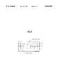
- FIGS. 1a to 1care sectional views of a semiconductor device showing a conventional method for forming the cobalt silicide layer in the source/drain region of the shallow junction.
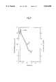
- FIG. 2is a graph of the distribution of dopant concentration of a conventional p/n junction.
- a P-type impurity ionis added to an n-type silicon substrate 1, thereby to form the source/drain junction on the substrate 1 as shown in FIG. 1a.
- boron ionsB ions
- a thin cobalt film 2is formed, by vapor deposition, on the silicon substrate 1 having the p/n junction and heated using RTP or a furnace at a high temperature not less than 700° C.
- the silicon (Si) of the silicon substrate 1reacts with the cobalt (Co) at the interface between the silicon substrate and the thin cobalt film 2.
- This reactionis represented by the reaction formula:
- a cobalt silicide (CoSi 2 ) layer 3is formed as shown in FIG. 1b.
- the time of this heat treatmentis controlled in order to form the desired shallow junction.
- part of the thin cobalt filmdoes not react with the silicon and remains as it was.
- FIG. 1bThe resulting structure of FIG. 1b is, thereafter, etched with a solution of 3HC1:1H 2 O 2 .
- a solution of 3HC1:1H 2 O 2As a result of this etching, only the remaining thin cobalt film 2 is etched and removed from the structure as shown in FIG. 1c since there is a difference of etching selection ratio between the remaining thin cobalt film 2 and the formed cobalt silicide layer 3.
- the above cobalt silicide formation methodhas several problems.
- the thickness of the formed silicide layer of that methodexceeds about 900 ⁇ and, as a result, this cobalt silicide formation method is rarely reproduced or duplicated when it is used to produce a shallow junction semiconductor device having a junction depth not more than 0.2 ⁇ m.
- use of such a silicidedeteriorates the characteristics of the semiconductor device.
- the contact resistanceis reduced as the dopant concentration of the silicon section just below the cobalt silicide (CoSi 2 ) layer is increased and the stability of the semiconductor device is improved in proportion to the distance between the silicide/silicon interface and the junction.
- the above cobalt silicide formation methodresults in a thick cobalt silicide layer of about 900 ⁇ being formed and consumes silicon as much as the thickness of the formed cobalt layer as represented in the graph of FIG. 3 showing redistribution of dopant concentration according to the above silicide layer formation method.
- a thick cobalt silicide layer of about 900 ⁇being formed and consumes silicon as much as the thickness of the formed cobalt layer as represented in the graph of FIG. 3 showing redistribution of dopant concentration according to the above silicide layer formation method.
- an object of the present inventionto provide a method for forming a silicide layer of a semiconductor device in which the aforementioned problems are overcome, which minimizes the silicon consumption, prevents redistribution of the dopant concentration and provides the desired shallow junction.
- a method for forming a silicide layer in accordance with an embodiment of the present inventioncomprises the steps of: forming a refractory metal layer and a thin cobalt film on a silicon substrate by vapor deposition under vacuum conditions; forming a silicide layer at an interface between the silicon substrate and the refractory metal layer by heat treatment; and etching and removing both the non-reacted thin cobalt film and the non-reacted refractory metal layer using the etching solution.
- Another definition of this inventionincludes a method for forming a silicide layer in a semiconductor device, including the steps of: forming a refractory metal layer on a semiconductor substrate; forming a cobalt layer on the refractory metal layer; implanting impurities in the interface between the refractory metal and the cobalt layer; heat treating the semiconductor substrate such that cobalt atoms from the cobalt layer pass through the refractory metal layer and form a cobalt silicide epitaxy layer on the semiconductor substrate; and removing the remaining cobalt layer and the remaining refractory metal layer.
- FIGS. 1a to 1care sectional views of a semiconductor device showing a conventional method for forming a cobalt silicide layer in a source/drain region of a shallow junction;
- FIG. 2is a graph showing a distribution of dopant concentration of a conventional p/n junction
- FIG. 3is a graph showing redistribution of dopant concentration according to the conventional silicide layer formation method
- FIGS. 4a to 4dare sectional views of a semiconductor device showing a method for forming a silicide layer in a source/drain region of shallow junction in accordance with an embodiment of the present invention
- FIG. 5is a spectrum of a silicide layer using Ta as a refractory metal in accordance with the present invention.
- FIG. 6is a spectrum of a silicide layer using Zr as a refractory metal in accordance with the present invention.
- FIG. 7is a graph showing the distribution of dopant concentration in accordance with the present invention.
- FIG. 8shows the preferential diffusion of the cobalt atoms into the substrate in accordance with the present invention.
- FIGS. 4a to 4dare sectional views of a semiconductor device showing a method for forming a silicide layer in a source/drain region of a shallow junction in accordance with an embodiment of the present invention.
- FIGS. 5 and 6are spectrums of silicide layers using Ta and Zr, respectively, as refractory metals according to the present invention.
- FIG. 7is a graph showing the distribution of dopant concentration in accordance with the present invention.
- p-type impurity ionsboron B
- boron Bare first implanted to an n-type silicon substrate 1 to form the source/drain junction on the substrate 1 as showing in FIG. 4a.
- the substrate 1 in which the p-type impurity ions are implantedis exposed to form a native oxide layer or film 4 on its surface. That is, in the case of formation of a p-type channel transistor, the boron (B) ions are implanted to the n-type silicon substrate 1 as represented in the graph of FIG. 7, thereby to form the source/drain junction on the substrate 1.
- a refractory metal layer 5such as a tantalum (Ta) layer, zirconium (Zr) layer or hafnium (Hf) layer is formed by vapor deposition on the silicon substrate 1 having the source/drain junction and a thin cobalt film 2 is formed by vapor deposition on the refractory metal layer 5 under the continued vacuum condition.
- a refractory metal layer 5such as a tantalum (Ta) layer, zirconium (Zr) layer or hafnium (Hf) layer is formed by vapor deposition on the silicon substrate 1 having the source/drain junction and a thin cobalt film 2 is formed by vapor deposition on the refractory metal layer 5 under the continued vacuum condition.
- the thickness of the refractory metal layer 5does not exceed 80 ⁇ and the thickness of the thin cobalt layer 2 does not exceed 250 ⁇ .
- Argon (Ar) ionsare implanted under conditions of energy (55 KeV) and dose (1 ⁇ 10 14 atoms/cm 2 ) so as to make the lower part of the cobalt layer 2 and the upper part of the substrate 1. amorphous, centering around the refractory metal layer S being an interlayer between the cobalt layer 2 and the substrate 1.
- a refractory metal 5such as Ta, Zr or Hf is formed on a p-type substrate 1 and a cobalt layer 2 is then formed on the refractory metal layer 5.
- V group of impurity ionssuch as phosphorous (P) and arsenic (As) are implanted under condition of energy (90 KeV) and dose (1 ⁇ 10 14 atoms/cm 2 ) so as to make the lower part of the cobalt layer 2 and the upper part of the substrate 1 amorphous, centering the refractory metal layer 5 being an interlayer between the substrate 1 and the cobalt layer 2, and also to form source/drain junctions.
- the above ion-implantationis followed by heat treatment (RTP).
- the heat treatmentis conducted for about twenty seconds at about 700° C. under nitrogen ambient or ammonium ambient.
- cobalt atoms of the thin cobalt film 2pass through the refractory metal layer 5 and form an epitaxy layer 6 of cobalt silicide CoSi 2 on the silicon substrate 1 as shown in FIG. 4c.
- the thickness of cobalt silicide layer 6does not exceed 200 ⁇ .
- non-reacted partsremain in both the thin cobalt film 2 and the refractory metal layer 5.
- the resulting structure of FIG. 4cis, thereafter, etched using a solution of 3HC1:1H 2 O 2 for about fifteen seconds. As a result of this etching, the remaining cobalt thin film 2 and the remaining refractory metal layer 5 except for the formed cobalt silicide layer 6 are etched and removed from the structure as shown in FIG. 4d.
- the refractory metal layer 5 formed by the vapor depositionreduces the native oxide layer 4 of the silicon substrate 1 during the heat treatment since its oxidation potential is larger than that of silicon.
- the refractory metal layer 5instead of the silicon substrate 1 is consumed during the silicide formation.
- the early silicide productis 300° C.
- the lattice constant of cobalt silicideis similar to that of silicon, so that the cobalt silicide is apt to grow into the epitaxy layer. Accordingly, the cobalt atoms pass through the refractory metal layer 5 during the heat treatment in order to reach the silicon substrate surface, from which surface the natural oxidant layer 4 was reduced and removed, and to form the cobalt silicide on the substrate surface.
- CoSi 2 solicaidethat is, self-aligned CoSi 2 silicide
- a bilayerconstituted by a C cobalt (Co) layer and a refractory metal layer
- spiking of CoSi 2may occur in part.
- the main reason why such spiking may occuris because Co atoms are preferentially diffused into the substrate 1 passing through the grain boundary as shown in FIG. 8.
- impurity ions of impuritiessuch as Ar, As and P are implanted to make the lower part of the cobalt layer and the upper part of the substrate 1 amorphous, centering around the refractory metal layer 5 being an interlayer between the cobalt layer 2 and the substrate 1, and moreover to prevent the preferential diffusion of cobalt atoms through the grain boundary.
- impurity ions of impuritiessuch as Ar, As and P are implanted to make the lower part of the cobalt layer and the upper part of the substrate 1 amorphous, centering around the refractory metal layer 5 being an interlayer between the cobalt layer 2 and the substrate 1, and moreover to prevent the preferential diffusion of cobalt atoms through the grain boundary.
- the processcan be simplified since an ion-implantation is carried out for both amorphous state and junction without carrying out the ion-implantation before forming the cobalt layer and the refractory metal layer.
- FIGS. 5 and 6are spectrums of silicide layers using Ta and Zr, respectively, as the refractory metal according to the present invention. Both the cobalt silicides of FIGS. 5 and 6 are formed by heat treatment at 750° C. As represented in the spectrums of FIGS. 5 and 6, the thickness of the cobalt silicide growing on the silicon substrate surface can be controlled by the refractory metal selected.
- the silicide formation method of the present inventionshows the following effects.
- the method of this inventionforms, by vapor deposition, a refractory metal layer on a silicon substrate having a junction and forms, by vapor disposition, a thin cobalt film on the formed refractory metal layer prior to heat treatment, thereby forming a shallow cobalt silicide layer of a thickness not exceeding 200 ⁇ in accordance with the refractory metal used.
- this methodeasily provides a shallow junction.
- this methodforms a shallow cobalt silicide layer at the interface of the silicon substrate by vapor deposition of the refractory metal layer on the silicon substrate having the junction and by vapor deposition of the thin cobalt film on the formed refractory metal layer and by heat treatment of the resulting structure.
- this methodprevents redistribution of the dopant, constituting the junction, as represented in the graph of FIG. 7.
- the cobalt silicide layer formed by this methodis preferably shallow, so that this method has the advantage that the dopant concentration at the interface between the silicon substrate and the cobalt silicide layer is not reduced.
- the cobalt silicide layer growing on the silicon substrateshows epitaxy characteristics, so that the interface between the cobalt silicide layer and the silicon substrate is flattened such that the desired processing stability is achieved.
- this methodimproves the electric characteristics of the semiconductor device.
Landscapes
- Engineering & Computer Science (AREA)
- Physics & Mathematics (AREA)
- Condensed Matter Physics & Semiconductors (AREA)
- General Physics & Mathematics (AREA)
- Manufacturing & Machinery (AREA)
- Computer Hardware Design (AREA)
- Microelectronics & Electronic Packaging (AREA)
- Power Engineering (AREA)
- Electrodes Of Semiconductors (AREA)
Abstract
Description
CoSi+Si=CoSi.sub.2 ( 1)
Claims (21)
Priority Applications (1)
| Application Number | Priority Date | Filing Date | Title |
|---|---|---|---|
| US08/524,457US5824600A (en) | 1993-01-19 | 1995-09-06 | Method for forming a silicide layer in a semiconductor device |
Applications Claiming Priority (4)
| Application Number | Priority Date | Filing Date | Title |
|---|---|---|---|
| KR616/1993 | 1993-01-19 | ||
| KR1019930000616AKR960006698B1 (en) | 1993-01-19 | 1993-01-19 | Silicide Formation Method |
| US18332994A | 1994-01-19 | 1994-01-19 | |
| US08/524,457US5824600A (en) | 1993-01-19 | 1995-09-06 | Method for forming a silicide layer in a semiconductor device |
Related Parent Applications (1)
| Application Number | Title | Priority Date | Filing Date |
|---|---|---|---|
| US18332994AContinuation-In-Part | 1993-01-19 | 1994-01-19 |
Publications (1)
| Publication Number | Publication Date |
|---|---|
| US5824600Atrue US5824600A (en) | 1998-10-20 |
Family
ID=26629499
Family Applications (1)
| Application Number | Title | Priority Date | Filing Date |
|---|---|---|---|
| US08/524,457Expired - Fee RelatedUS5824600A (en) | 1993-01-19 | 1995-09-06 | Method for forming a silicide layer in a semiconductor device |
Country Status (1)
| Country | Link |
|---|---|
| US (1) | US5824600A (en) |
Cited By (8)
| Publication number | Priority date | Publication date | Assignee | Title |
|---|---|---|---|---|
| US6096647A (en)* | 1999-10-25 | 2000-08-01 | Chartered Semiconductor Manufacturing Ltd. | Method to form CoSi2 on shallow junction by Si implantation |
| US6187617B1 (en)* | 1999-07-29 | 2001-02-13 | International Business Machines Corporation | Semiconductor structure having heterogeneous silicide regions and method for forming same |
| US6413859B1 (en)* | 2000-03-06 | 2002-07-02 | International Business Machines Corporation | Method and structure for retarding high temperature agglomeration of silicides using alloys |
| US20040266153A1 (en)* | 2003-06-26 | 2004-12-30 | Hu Yongjun Jeff | Methods of forming metal silicide |
| US20070032071A1 (en)* | 2005-08-02 | 2007-02-08 | Micron Technology, Inc. | Methods of forming CoSi2, methods of forming field effect transistors, and methods of forming conductive contacts |
| US20090011566A1 (en)* | 2007-07-03 | 2009-01-08 | Renesas Technology Corp. | Method of manufacturing semiconductor device |
| US20100013029A1 (en)* | 2008-07-18 | 2010-01-21 | Harry Chuang | Structure and a Method of Manufacture for Low Resistance NiSix |
| US20150372110A1 (en)* | 2013-07-17 | 2015-12-24 | Huawei Technologies Co., Ltd. | Semiconductor fin fabrication method and fin fet device fabrication method |
Citations (7)
| Publication number | Priority date | Publication date | Assignee | Title |
|---|---|---|---|---|
| US5047364A (en)* | 1988-06-27 | 1991-09-10 | Mitsubishi Denki Kabushiki Kaisha | Method for making a multi-point emission type semiconductor laser device |
| JPH042121A (en)* | 1990-04-18 | 1992-01-07 | Nippondenso Co Ltd | Manufacture of titanium silicide |
| US5210043A (en)* | 1989-09-26 | 1993-05-11 | Seiko Instruments Inc. | Process for producing semiconductor device |
| US5344793A (en)* | 1993-03-05 | 1994-09-06 | Siemens Aktiengesellschaft | Formation of silicided junctions in deep sub-micron MOSFETs by defect enhanced CoSi2 formation |
| US5352631A (en)* | 1992-12-16 | 1994-10-04 | Motorola, Inc. | Method for forming a transistor having silicided regions |
| US5356837A (en)* | 1993-10-29 | 1994-10-18 | International Business Machines Corporation | Method of making epitaxial cobalt silicide using a thin metal underlayer |
| US5536684A (en)* | 1994-06-30 | 1996-07-16 | Intel Corporation | Process for formation of epitaxial cobalt silicide and shallow junction of silicon |
- 1995
- 1995-09-06USUS08/524,457patent/US5824600A/ennot_activeExpired - Fee Related
Patent Citations (7)
| Publication number | Priority date | Publication date | Assignee | Title |
|---|---|---|---|---|
| US5047364A (en)* | 1988-06-27 | 1991-09-10 | Mitsubishi Denki Kabushiki Kaisha | Method for making a multi-point emission type semiconductor laser device |
| US5210043A (en)* | 1989-09-26 | 1993-05-11 | Seiko Instruments Inc. | Process for producing semiconductor device |
| JPH042121A (en)* | 1990-04-18 | 1992-01-07 | Nippondenso Co Ltd | Manufacture of titanium silicide |
| US5352631A (en)* | 1992-12-16 | 1994-10-04 | Motorola, Inc. | Method for forming a transistor having silicided regions |
| US5344793A (en)* | 1993-03-05 | 1994-09-06 | Siemens Aktiengesellschaft | Formation of silicided junctions in deep sub-micron MOSFETs by defect enhanced CoSi2 formation |
| US5356837A (en)* | 1993-10-29 | 1994-10-18 | International Business Machines Corporation | Method of making epitaxial cobalt silicide using a thin metal underlayer |
| US5536684A (en)* | 1994-06-30 | 1996-07-16 | Intel Corporation | Process for formation of epitaxial cobalt silicide and shallow junction of silicon |
Non-Patent Citations (14)
| Title |
|---|
| "A Self-Aligned CoSi2 Interconnection and Contact Technology for VLSI Applications" by L. Van Den Hove, et al., published in IEEE Transactions on Electron Devices, vol. ED-34, No. 3, Mar. 1987. |
| "A Study of the Leakage Mechanisms of Silicided n+/p Junctions" by R. Liu, et al., published in J.Appl. Phys. 63 (6) on Mar. 15, 1988. |
| "Application of Self-Aligned CoSi2 Interconnection in Submicrometer CMOS Transistors" by E.K. Broadbent, et al., published in IEEE Transactions on Electron Devices, vol. 36, No. 11, Nov. 1989. |
| "Process Limitation and Device Design Tradeoffs of Self-Aligned TiSi2 Junction Formation in Submicrometer CMOS Devices" by Chih-Yuan Lu, et al., published in IEEE Transactions on Electron Devices, vol. 38, No. 2, Feb. 1991. |
| "Self-Aligned Silicided (PtSi and CoSi2) Ultra-Shallow p+/n Junctions" by E.K. Broadbent, et al., published in IEEE Electron Device Letters, vol. EDL-8, No. 7, Jul. 1987. |
| "VLSI Technology" by S.M. Sze, published by McGraw-Hill Book Company. 1987. |
| A Self Aligned CoSi 2 Interconnection and Contact Technology for VLSI Applications by L. Van Den Hove, et al., published in IEEE Transactions on Electron Devices, vol. ED 34, No. 3, Mar. 1987.* |
| A Study of the Leakage Mechanisms of Silicided n /p Junctions by R. Liu, et al., published in J.Appl. Phys. 63 (6) on Mar. 15, 1988.* |
| Application of Self Aligned CoSi 2 Interconnection in Submicrometer CMOS Transistors by E.K. Broadbent, et al., published in IEEE Transactions on Electron Devices, vol. 36, No. 11, Nov. 1989.* |
| Physics of Semiconductor Devices, Second Edition, by S.M. Sze, published by John Wiley & Sons in 1981.* |
| Process Limitation and Device Design Tradeoffs of Self Aligned TiSi 2 Junction Formation in Submicrometer CMOS Devices by Chih Yuan Lu, et al., published in IEEE Transactions on Electron Devices, vol. 38, No. 2, Feb. 1991.* |
| Self Aligned Silicided (PtSi and CoSi 2 ) Ultra Shallow p /n Junctions by E.K. Broadbent, et al., published in IEEE Electron Device Letters, vol. EDL 8, No. 7, Jul. 1987.* |
| Semiconductor Devices Physics and Technology by S.M. Sze, published by John Wiley & Sons in 1983.* |
| VLSI Technology by S.M. Sze, published by McGraw Hill Book Company. 1987.* |
Cited By (19)
| Publication number | Priority date | Publication date | Assignee | Title |
|---|---|---|---|---|
| US6187617B1 (en)* | 1999-07-29 | 2001-02-13 | International Business Machines Corporation | Semiconductor structure having heterogeneous silicide regions and method for forming same |
| US6512296B1 (en) | 1999-07-29 | 2003-01-28 | International Business Machines Corporation | Semiconductor structure having heterogenous silicide regions having titanium and molybdenum |
| US6096647A (en)* | 1999-10-25 | 2000-08-01 | Chartered Semiconductor Manufacturing Ltd. | Method to form CoSi2 on shallow junction by Si implantation |
| US6413859B1 (en)* | 2000-03-06 | 2002-07-02 | International Business Machines Corporation | Method and structure for retarding high temperature agglomeration of silicides using alloys |
| US7282443B2 (en)* | 2003-06-26 | 2007-10-16 | Micron Technology, Inc. | Methods of forming metal silicide |
| US20040266153A1 (en)* | 2003-06-26 | 2004-12-30 | Hu Yongjun Jeff | Methods of forming metal silicide |
| US7030014B2 (en) | 2003-06-26 | 2006-04-18 | Micron Technology, Inc. | Semiconductor constructions and electronic systems comprising metal silicide |
| US20040266119A1 (en)* | 2003-06-26 | 2004-12-30 | Hu Yongjun Jeff | Semiconductor constructions comprising metal silicide |
| US20090035938A1 (en)* | 2005-08-02 | 2009-02-05 | Yongjun Jeff Hu | Methods of Forming CoSi2, Methods of Forming Field Effect Transistors, and Methods of Forming Conductive Contacts |
| US7449410B2 (en)* | 2005-08-02 | 2008-11-11 | Micron Technology, Inc. | Methods of forming CoSi2, methods of forming field effect transistors, and methods of forming conductive contacts |
| US20070032071A1 (en)* | 2005-08-02 | 2007-02-08 | Micron Technology, Inc. | Methods of forming CoSi2, methods of forming field effect transistors, and methods of forming conductive contacts |
| US7989340B2 (en) | 2005-08-02 | 2011-08-02 | Micron Technology, Inc. | Methods of forming CoSi2, methods of forming field effect transistors, and methods of forming conductive contacts |
| US8435889B2 (en) | 2005-08-02 | 2013-05-07 | Micron Technology, Inc. | Methods of forming CoSi2, methods of forming field effect transistors, and methods of forming conductive contacts |
| US20090011566A1 (en)* | 2007-07-03 | 2009-01-08 | Renesas Technology Corp. | Method of manufacturing semiconductor device |
| US7955925B2 (en)* | 2007-07-03 | 2011-06-07 | Renesas Electronics Corporation | Method of manufacturing semiconductor device |
| US20100013029A1 (en)* | 2008-07-18 | 2010-01-21 | Harry Chuang | Structure and a Method of Manufacture for Low Resistance NiSix |
| US8349732B2 (en) | 2008-07-18 | 2013-01-08 | Taiwan Semiconductor Manufacturing Company, Ltd. | Implanted metal silicide for semiconductor device |
| US20150372110A1 (en)* | 2013-07-17 | 2015-12-24 | Huawei Technologies Co., Ltd. | Semiconductor fin fabrication method and fin fet device fabrication method |
| US9698253B2 (en)* | 2013-07-17 | 2017-07-04 | Huawei Technologies Co., Ltd. | Semiconductor fin fabrication method and Fin FET device fabrication method |
Similar Documents
| Publication | Publication Date | Title |
|---|---|---|
| US5721175A (en) | Method of manufacturing a semiconductor device | |
| Morimoto et al. | Self-aligned nickel-mono-silicide technology for high-speed deep submicrometer logic CMOS ULSI | |
| US5567651A (en) | Self-aligned cobalt silicide on MOS integrated circuits | |
| US6127249A (en) | Metal silicidation methods and methods for using same | |
| US6159856A (en) | Method of manufacturing a semiconductor device with a silicide layer | |
| US5967794A (en) | Method for fabricating a field effect transistor having elevated source/drain regions | |
| EP0109082A2 (en) | Method of manufacturing a semiconductor device comprising a diffusion step | |
| US6329277B1 (en) | Method of forming cobalt silicide | |
| JPH0945907A (en) | Manufacture of semiconductor device | |
| JPH0774128A (en) | Self-aligned silicide process | |
| JPH05136086A (en) | Semiconductor manufacturing process for providing local interconnecting structure | |
| US6555453B1 (en) | Fully nickel silicided metal gate with shallow junction formed | |
| WO1994000878A1 (en) | Methods of forming a local interconnect and a high resistor polysilicon load | |
| US5824600A (en) | Method for forming a silicide layer in a semiconductor device | |
| US6096599A (en) | Formation of junctions by diffusion from a doped film into and through a silicide during silicidation | |
| Öztürk et al. | Rapid thermal chemical vapor deposition of germanium on silicon and silicon dioxide and new applications of Ge in ULSI technologies | |
| US5963829A (en) | Method of forming silicide film | |
| JP2559669B2 (en) | Method of forming silicide film | |
| US6828206B2 (en) | Semiconductor device and method for fabricating the same | |
| JPH05304108A (en) | Semiconductor device and fabrication thereof | |
| US5998286A (en) | Method to grow self-aligned silicon on a poly-gate, source and drain region | |
| JP3044849B2 (en) | Method for manufacturing semiconductor device | |
| GB2177255A (en) | VLSI MOSFET circuits using refractory metal and/or refractory metal silicide | |
| JP2003218060A (en) | Method for manufacturing semiconductor device | |
| JP2900897B2 (en) | Method for manufacturing semiconductor device |
Legal Events
| Date | Code | Title | Description |
|---|---|---|---|
| AS | Assignment | Owner name:LG SEMICON CO., LTD., KOREA, REPUBLIC OF Free format text:CHANGE OF NAME;ASSIGNOR:GOLDSTAR ELECTRON CO., LTD.;REEL/FRAME:007658/0783 Effective date:19960208 | |
| AS | Assignment | Owner name:LG SEMICON CO., LTD., KOREA, REPUBLIC OF Free format text:ASSIGNMENT OF ASSIGNORS INTEREST;ASSIGNORS:BYUN, JEONG SOO;KIM, HYUNG JUN;REEL/FRAME:008134/0809 Effective date:19960430 | |
| FEPP | Fee payment procedure | Free format text:PAYOR NUMBER ASSIGNED (ORIGINAL EVENT CODE: ASPN); ENTITY STATUS OF PATENT OWNER: LARGE ENTITY | |
| FPAY | Fee payment | Year of fee payment:4 | |
| FPAY | Fee payment | Year of fee payment:8 | |
| FEPP | Fee payment procedure | Free format text:PAYER NUMBER DE-ASSIGNED (ORIGINAL EVENT CODE: RMPN); ENTITY STATUS OF PATENT OWNER: LARGE ENTITY Free format text:PAYOR NUMBER ASSIGNED (ORIGINAL EVENT CODE: ASPN); ENTITY STATUS OF PATENT OWNER: LARGE ENTITY | |
| REMI | Maintenance fee reminder mailed | ||
| LAPS | Lapse for failure to pay maintenance fees | ||
| STCH | Information on status: patent discontinuation | Free format text:PATENT EXPIRED DUE TO NONPAYMENT OF MAINTENANCE FEES UNDER 37 CFR 1.362 | |
| FP | Lapsed due to failure to pay maintenance fee | Effective date:20101020 |