US5824584A - Method of making and accessing split gate memory device - Google Patents
Method of making and accessing split gate memory deviceDownload PDFInfo
- Publication number
- US5824584A US5824584AUS08/876,326US87632697AUS5824584AUS 5824584 AUS5824584 AUS 5824584AUS 87632697 AUS87632697 AUS 87632697AUS 5824584 AUS5824584 AUS 5824584A
- Authority
- US
- United States
- Prior art keywords
- gate
- forming
- doped layer
- voltage
- semiconductor
- Prior art date
- Legal status (The legal status is an assumption and is not a legal conclusion. Google has not performed a legal analysis and makes no representation as to the accuracy of the status listed.)
- Expired - Lifetime
Links
Images

Classifications
- H—ELECTRICITY
- H10—SEMICONDUCTOR DEVICES; ELECTRIC SOLID-STATE DEVICES NOT OTHERWISE PROVIDED FOR
- H10B—ELECTRONIC MEMORY DEVICES
- H10B43/00—EEPROM devices comprising charge-trapping gate insulators
- H10B43/40—EEPROM devices comprising charge-trapping gate insulators characterised by the peripheral circuit region
- H—ELECTRICITY
- H10—SEMICONDUCTOR DEVICES; ELECTRIC SOLID-STATE DEVICES NOT OTHERWISE PROVIDED FOR
- H10B—ELECTRONIC MEMORY DEVICES
- H10B41/00—Electrically erasable-and-programmable ROM [EEPROM] devices comprising floating gates
- Y—GENERAL TAGGING OF NEW TECHNOLOGICAL DEVELOPMENTS; GENERAL TAGGING OF CROSS-SECTIONAL TECHNOLOGIES SPANNING OVER SEVERAL SECTIONS OF THE IPC; TECHNICAL SUBJECTS COVERED BY FORMER USPC CROSS-REFERENCE ART COLLECTIONS [XRACs] AND DIGESTS
- Y10—TECHNICAL SUBJECTS COVERED BY FORMER USPC
- Y10S—TECHNICAL SUBJECTS COVERED BY FORMER USPC CROSS-REFERENCE ART COLLECTIONS [XRACs] AND DIGESTS
- Y10S438/00—Semiconductor device manufacturing: process
- Y10S438/933—Germanium or silicon or Ge-Si on III-V
Definitions
- This inventionrelates in general to non-volatile memory devices, and more particularly to high density, split-gate nonvolatile memory devices capable of operating a low power supply voltages, and to methods for operating and fabricating such devices.
- non-volatile memory devicesare typically constructed by fabricating a field effect transistor in a silicon substrate.
- the field effect transistoris capable of storing electrical charge either in a separate gate electrode, known as a floating gate, or in a dielectric layer underlying a control gate electrode.
- Datais stored in a non-volatile memory device by changing the threshold voltage of the field effect transistor through the storage of electrical charge over the channel region of the substrate.
- an accumulation of electrons in a floating gate electrode, or in a dielectric layer overlying the channel regioncreates a high threshold voltage in the field effect transistor.
- the control gateWhen the control gate is grounded, current will not flow through the transistor, which is defined as being in a logic zero state. Conversely, a reduction in the negative charge over the channel region creates a low threshold voltage, possibly negative. In this condition, with the control gate grounded, current will flow through the field effect transistor, which is defined as being in a logic one state.
- Flash EEPROMelectrically-erasable-programmable-read-only-memory
- Flash EEPROMsare a type of device which provide electrical erasing capability.
- flashrefers to the ability to erase the memory cells simultaneously with electrical pulses. In the erased state, the threshold voltage of the field effect transistor is low and electrical current can flow through the transistor indicating a logic 1 state.
- drain-side hot-electron injectionis used to inject electrons onto either a floating gate electrode, or into trapping sites in a dielectric film overlying the channel region.
- the injection currentcan be enhanced by increasing either the channel electric field, or the electric field in the dielectric layer.
- very high drain and gate voltagesare used, such that the transistor is operating very close to breakdown during programming.
- the high voltages necessary for drain-side injectionrequire that an additional power supply be provided to supply voltage levels in excess of the standard 5-volt operating voltage.
- Breakdown conditions during programmingcan be avoided by injecting electrons from the source region, rather than the drain region.
- a select gate electrodeis formed overlying a portion of the channel region adjacent to the source region.
- the select gate electrodeis electrically isolated from the control gate electrode, which is formed adjacent to the drain region.
- an electric field gradientis established in the channel region such that electrons originating in the source region are accelerated across a potential drop, and are injected onto a floating gate electrode located below the control gate electrode.
- Programming with source side injectionincreases the longevity of an EEPROM device by reducing the stress on the dielectric layer as compared with the excessive electric fields used for drain-side injection. Additionally, it has been demonstrated that source-side injection can be many times more efficient than drain side injection. The higher efficiency reduces the amount of time necessary to perform a programming operation.
- Another single gate EEPROM devicehas been formed by doping gate oxide with germanium, and eliminating the floating gate. By modifying the gate oxide composition of the device, the ability to integrate logic and memory cells on a common substrate becomes infeasible without greatly increasing the manufacturing complexity of the device.
- One type of EEPROM device using source side injectionrequires that three separate semiconductor layers be provided for the fabrication of a select gate, a control gate, and a floating gate. In practice, these three layers are typically formed from three polysilicon layers.
- Another type of source-side injection EEPROM deviceuses two polysilicon layers to form a select gate and a sidewall gate which are separated by an oxide-nitride-oxide (ONO) stack.
- ONOoxide-nitride-oxide
- the use of a sidewall gate in a EEPROM deviceenables one to form higher density memory arrays. Furthermore, fabrication of a sidewall gate device is considered to be simpler than that of a floating gate device due to a fewer number of processing steps.
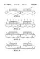
- FIGS. 1-6illustrate, in cross-section, a portion of a semiconductor device which include both a non-volatile memory portion and a logic portion fabricated in accordance with one embodiment of the present invention.
- FIG. 7illustrates current versus voltage (I-V) curves of a sidewall gate transistor having a germanium doped oxide in accordance with the present invention as compared to a sidewall gate transistor having an ONO as in the prior art.
- the present inventionprovides a semiconductor device which includes a non-volatile memory, and more particularly a EEPROM, that has improved threshold characteristics and a simpler fabrication flow as compared to prior art devices which include non-volatile memories. More particularly, the present invention utilizes a sidewall gate transistor in conjunction with a semiconductor doped oxide, or dielectric, to form a non-volatile memory cell.
- the semiconductor element used to dope the oxidewill generally include silicon or germanium.
- Use of the doped oxide layersimplifies the fabrication process by eliminating the need to deposit and etch ONO layers. Deposition and densification of the ONO layers is a time consuming portion of the fabrication process due to the high temperature and long processing times involved.
- the present inventionallows for implementation of logic and memory cells on a common substrate without increasing the number of processing steps.
- FIGS. 1-7It is important to point out that the figures are not necessarily drawn to scale, and that there are likely to be other embodiments of the invention which are not specifically illustrated.
- FIGS. 1-6illustrate in cross-section a portion of a semiconductor device 5 which includes a non-volatile memory portion 7 and a logic portion 9 in accordance with one embodiment of the present invention.
- semiconductor device 5includes a semiconductor substrate 10 having an overlying dielectric layer 12 and a first gate electrode 14 and a second gate electrode 16.
- substrate 10will be formed of a single crystal semiconductor material such as silicon and dielectric layer 12 will be formed of a dielectric such as silicon dioxide.
- gate electrodes 14 and 16are preferably formed of polysilicon.
- Gate electrode 14will serve as a select gate for the non-volatile memory device of semiconductor device 5 while gate electrode 16 will serve as a control gate electrode for a transistor to be formed in the logic portion of the device.
- Dielectric layer 12serves as the gate oxide for both the non-volatile and logic devices, and preferably is formed to a thickness in the range of 30-300 angstroms, and will generally be approximately 100 angstroms for a low voltage passing transistor and 250 angstroms for high voltage passing transistors.
- Oxide layer 20is deposited over both portions of the device as illustrated in FIG. 2.
- Oxide layer 20is again preferably silicon dioxide thermally grown or chemical vapor deposited to a thickness in the range of 30-500 angstroms, and in general this thickness will be in the low end of this range for low voltage and low power applications.
- semiconductor device 5undergoes an implantation step to implant semiconductor atoms 21, such as germanium or silicon, into the oxide layer.
- the implantation stepis a blanket implantation, in that the dopant atoms 21 are introduced across both portions of device 5.
- the goal in implanting the dopant species in oxide layer 20is to concentrate a region of dopants into the oxide layer.
- the concentration or projected range of dopant atoms 21will be substantially within the oxide layer such that the greatest concentration will be near approximately the center of the dielectric layer 12.
- germanium dopant atoms into the oxideat a dosage of 1E15 to 1E16 at an energy of 5-10 kev has been found to provide a suitable profile of dopant atoms for purposes of practicing the present invention.
- dopant atomsFor doping with silicon atoms, it is expected that a lower energy is to be used with roughly the same dosage. While germanium and silicon dopant atoms are used in preferred embodiments of the present invention, it is envisioned that other dopant atoms can be used to achieve the same or similar results. As will be subsequently discussed, the desire is that whatever dopant atoms are used, that they are to be tightly concentrated or consolidated within the center of the oxide layer 12. For example, implantation of the heavy metals such as tungsten or molybdenum may be suitable because the projected standard deviation of implanting these materials is relatively small. Accordingly, the concentration of the dopant atoms can be tightly tailored to be at a specific location inside the oxide.
- a sidewall gate 28is formed along the electrode 14 within the non-volatile memory portion of semiconductor device 5. Sidewall gate 28 is separated from the gate electrode 14 by oxide layer 20.
- a blanket layer of polysilicon or other suitable gate materialis deposited across both the non-volatile and logic portions of semiconductor device 5. This polysilicon layer is deposited to a thickness no greater than the thickness of gate electrodes 14 and 16, and is deposited at least to a thickness to enable formation of a sidewall spacer using an anisotropic etch technique.
- semiconductor device 5is subjected to dry anisotropic etch which results in the formation of polysilicon sidewall spacers formed along each sidewall of both gate electrode 14 and gate electrode 16 within the device 5.
- a maskis formed to protect what will be the source side of the transistor within the non-volatile memory portion 7 of device 5.
- a maskcan be formed using conventional photoresist and photolithography techniques. After formation of such a mask, semiconductor device 5 is again subjected to an etch to remove all polysilicon in the unprotected areas.
- semiconductor device 5is subjected to an etch to remove portions of oxide layer 20 as illustrated in FIG. 4.
- the oxide etchis performed selectively to underlying silicon and polysilicon members, for example by using a dry etch or wet HF (hydrogen fluoride) etch chemistry.
- the oxide layeris removed in both the non-volatile memory portion 7 and the logic portion of the device, leaving the oxide layer 20 present only between sidewall gate 28 and gate electrode 14 and semiconductor substrate 10.
- a dedicated oxide removal stepas represented in going from FIG. 3 to FIG. 4 may not be required in actual practice.
- semiconductor device 5is likely to undergo one or more cleaning operations. These cleaning operations may adequately remove oxide layer 20 across device 5 such that a separate oxide removal step is not needed.
- a dielectric layer 30is deposited over the device to protect sidewall gate 28 from a subsequent silicidation process and to enable formation of a dielectric spacer adjacent to sidewall gate 28 to provide an adequate offset of a self-aligned source region from the sidewall gate electrode (i.e., to provide an effective channel length).
- a dielectric layer 30is deposited over device 5, followed by deposition of a silicon nitride layer 32.
- oxide layer 30is deposited using tetraethylorthosilicate (TEOS) and is deposited to a thickness of between 100-200 angstroms.
- TEOStetraethylorthosilicate
- Silicon nitride layer 32is preferably deposited by CVD to a thickness of between 500 and 3,000 angstroms.
- the purpose of oxide layer 30is to enable sidewall spacers to be formed from silicon nitride layer 32, without attacking the underlying silicon substrate during the spacer etch.
- oxide layer 30serves as an etch stop.
- oxide layeris not necessary, if there is a sufficient thickness of oxide or another etch stop material subsequently formed on exposed portions of semiconductor device 10 to provide an adequate etch stop during the spacer etch.
- first and second gatesare contacted in a conventional manner.
- semiconductor device 5is subjected to an anisotropic etch to form nitride sidewall spacers 36 along both sidewalls of both gate electrode 14 and gate electrode 16.
- nitride spacers 36Following formation of nitride spacers 36, convention ion implantation is used to form a source region 38 and a drain region 40 in the non-volatile portion 7 of device 5, while simultaneously forming a source region 42 and a drain region 44 for the transistor and the logic portion of semiconductor device 5.
- the presence of nitride spacers 36enable the source and drain regions to be formed in a self-aligned manner. It should be noted, that a nitride spacer would not be needed, if the width of the sidewall gate is sufficiently large to create an effective channel length for operating the transistor. Generally, the advantage of using the sidewall spacer is that improved density can be obtained.
- an annealing stepneeds to occur.
- the step of annealingallows the formation of a locally concentrated area of the implanted species where charges can be trapped and stored.
- the locally concentrated area of the implanted specieswill generally have a greater concentration than prior to the annealing step.
- the step of annealingcan be performed independently, but in a preferred embodiment is the result of subsequent source and drain activation anneal step.
- the formation of the dopant concentrated areaallows for charge to be stored which will effect the Vt of the sidewall transistor, allowing it to operation in a non-volatile manner. In one embodiment, it is believed that microcrystals of the semiconductor element are formed.
- FIG. 7illustrates I-V characteristics of the present invention, as compared to the prior art.
- Lines 71 and 76represent an erased sidewall transistor using the prior art and the present invention respectively.
- the present inventionprovides an improved subthreshold slope as compared to the prior art.
- Curves 73 and 78represent an programmed sidewall transistor using the prior art and the present invention respectively. Similar to the preceding discussion, the curve 78 illustrates that the present invention provides a better subthreshold slope than the prior art.
- the advantagesoriginate from the fact that thicker thermally grown oxide is used and no CVD oxide and nitride is used as in the prior art.
- a programming drain voltagesuch as, for example, a ground voltage is applied to drain region 40.
- a programming select gate voltage that is higher than the programming drain voltage by at least a threshold voltage of the portion of the channel region under select gate 14is applied to select gate 14.
- a programming source voltage that is higher than the programming drain voltageis applied to source region 38.
- a programming control gate voltage that is higher than the programming source voltageis applied to control gate 28.
- the programming select gate voltageis between approximately one volt and approximately two volts
- the programming source voltageis between approximately three volts and approximately six volts
- the programming control gate voltageis between approximately eight volts and approximately ten volts.
- source region 38is at a higher voltage level than drain region 40, n-channel FET including gates 14 and 28 operates in a reverse active mode.
- source region 38functions as a drain of the FET of FIG. 6, and drain region 40 functions as a source of during the programming process.
- select gate 14is at a voltage level higher than the voltage level of drain region 40 by at least a threshold voltage of the portion of channel region under select gate 14.
- Negative charge carrierse.g., electrons, originate from drain region 40 and are accelerated through the portion of channel region between select gate 14 and control gate 28.
- the charge carriersWhen they reach the portion the channel region adjacent source region 38 and under control gate 28, the charge carriers are attracted by the high voltage at control gate 28.
- the charge carriersIn a hot carrier injection process, the charge carriers are injected across the doped oxide layer 20 and trapped in the dopant concentrated area formed during the steps described previously.
- the negative charge carrierse.g., electrons
- a threshold voltage of the portion of channel region under control gate 28increases.
- the current flowing through channel regiondecreases and so does the rate of hot carrier injection.
- the programming voltagesare removed from the non-volatile memory (NVM)
- the injected carriersremain trapped in the dopant concentrated area of the doped oxide layer 20.
- a first logic valuee.g., a logic one, is stored in the NVM cell, i.e., the NVM cell is programmed.
- the programming select gate voltageis slightly above the threshold voltage of the portion of channel region under select gate 16, thereby allowing a small current flowing in channel region 38.
- process of programming The NVM cellis power efficient and suitable for low voltage and low power applications.
- an erasing source voltageis applied to source region 38, and an erasing control gate voltage that is lower than the erasing source voltage is applied to control gate 28.
- the erasing source voltageis between approximately five volts and approximately seven volts
- the erasing control gate voltageis between approximately -8 volts and approximately -9 volts.
- the select gate and drain regionsdo not participate in the erasing process, and they can be either coupled to a reference voltage level, e.g., ground voltage level, or floating.
- an erasing drain voltage of approximately 1.8 voltsis applied to the drain 40. This drain voltage embodiment of the present invention has been demonstrated to increase the life expectancy of a device by more than an order of magnitude.
- a strong electric fieldis established in the overlap portion of source region under control gate 28.
- the strong electric fieldgenerates electron-hole pairs in the overall region of source 38 and control gate 28.
- the holeswhich are positive charge carriers, gain energy through the electric field at the source edge and are attracted by the negative voltage at control gate 28. This varies from the prior art which uses a hot carrier injection process, where the holes are injected across an oxide layer into silicon nitride layer 24 of ONO stack 25, where they combine with the electrons in silicon nitride layer 24.
- the erasing processcontinues until the oxide layer 20 become substantially electrically neutral or positively charged. After the erasing voltages are removed from the NVM cell, the doped oxide layer 20 remains substantially neutral or positively charged. In either case, a second logic value, e.g., a logic zero, is stored in NVM cell, i.e., The NVM cell is erased.
- a second logic valuee.g., a logic zero
- the charges stored in the dopant concentrated area in layer 20are neutralized by charges of opposite polarity injected from channel region 38. This differs from the erasing process of the prior art, in which the charge stored in the charge trapping sites move to a control gate in a Fowler-Nordheim tunneling process through a dielectric layer between the charge trapping sites and the control gate.
- a reading source voltagesuch as, for example, ground voltage is applied to source region 38.
- a reading control gate voltagethat is substantially equal to or higher than the reading source voltage is applied to control gate 28.
- a reading select gate voltagethat is higher than the reading source voltage by at least a threshold voltage of the portion of channel region under select gate 14 is applied to select gate 16.
- the portion of channel region under select gate 14is switched on and conductive.
- a reading drain voltage that is higher than the reading source voltageis applied to drain region 40.
- the reading control gate voltageis between approximately one volt and approximately two volts
- the reading drain voltageis between approximately one volts and approximately two volt
- select gate 16is coupled to a supply voltage, V DD .
- the supply voltage V DDranges between approximately three volts and approximately five volts. In low power applications, the supply voltage V DD usually ranges between, for example, approximately 0.9 volt and approximately 1.8 volts.
- the portion of channel region under control gate 28has a threshold voltage that is higher than its intrinsic threshold voltage when silicon nitride layer 24 are substantially neutral. If the NVM cell has been erased, the doped region 20 is substantially neutral or positively charged.
- the portion of channel region under control gate 28has a threshold voltage that is substantially equal to or lower than its intrinsic threshold voltage.
- the reading control gate voltageis preferably lower than the threshold voltage of the portion of channel region under control gate 28 if the NVM cell has been programmed. In addition, the reading control gate voltage is preferably higher than the threshold voltage of the portion of channel region under control gate 28 if The NVM cell has been erased.
- channel regionis nonconductive and the current flowing therethrough is small, e.g., equal to or less than approximately 2 micro-amperes ( ⁇ A).
- a sense amplifiercoupled to drain region 40 via a bit line (not shown in FIG. 1) senses the small current and reads the first logic value, e.g., logic one, from The NVM cell.
- the sense amplifiercoupled to drain region 40 senses the large current and reads the second logic value, logic zero, from The NVM cell.
- source region 38is at a lower voltage level than drain region 40.
- the voltage drop across the portion of channel region under control gate 28is small.
- the probability of charge carriers being inadvertently injected from channel region into the oxide layer 20is small.
- the disturbance to the data stored in The NVM cell during the reading processis small.
- the sense amplifier(not shown) is coupled to drain region 40 via a bit line (not shown in FIG. 1) and drain region 40 is separated from silicon nitride layer 24 by select gate 14. Therefore, the capacitance of a parasitic bit line capacitor is substantially independent of the charges in silicon nitride layer 24. In other words, the data dependence of the parasitic bit line capacitance is small in The NVM cell.
- An NVM cell, such as The NVM cell, having a small data dependence of the bit line capacitanceis suitable for high performance applications.
Landscapes
- Non-Volatile Memory (AREA)
- Semiconductor Memories (AREA)
Abstract
Description
Claims (14)
Priority Applications (1)
| Application Number | Priority Date | Filing Date | Title |
|---|---|---|---|
| US08/876,326US5824584A (en) | 1997-06-16 | 1997-06-16 | Method of making and accessing split gate memory device |
Applications Claiming Priority (1)
| Application Number | Priority Date | Filing Date | Title |
|---|---|---|---|
| US08/876,326US5824584A (en) | 1997-06-16 | 1997-06-16 | Method of making and accessing split gate memory device |
Publications (1)
| Publication Number | Publication Date |
|---|---|
| US5824584Atrue US5824584A (en) | 1998-10-20 |
Family
ID=25367452
Family Applications (1)
| Application Number | Title | Priority Date | Filing Date |
|---|---|---|---|
| US08/876,326Expired - LifetimeUS5824584A (en) | 1997-06-16 | 1997-06-16 | Method of making and accessing split gate memory device |
Country Status (1)
| Country | Link |
|---|---|
| US (1) | US5824584A (en) |
Cited By (53)
| Publication number | Priority date | Publication date | Assignee | Title |
|---|---|---|---|---|
| US6177318B1 (en)* | 1999-10-18 | 2001-01-23 | Halo Lsi Design & Device Technology, Inc. | Integration method for sidewall split gate monos transistor |
| US6187636B1 (en)* | 1997-03-14 | 2001-02-13 | Hyundai Electronics Industries Co., Ltd. | Flash memory device and fabrication method thereof |
| US6228695B1 (en) | 1999-05-27 | 2001-05-08 | Taiwan Semiconductor Manufacturing Company | Method to fabricate split-gate with self-aligned source and self-aligned floating gate to control gate |
| US6259133B1 (en)* | 1999-02-11 | 2001-07-10 | Advanced Micro Devices, Inc. | Method for forming an integrated circuit memory cell and product thereof |
| US6274479B1 (en)* | 1998-08-21 | 2001-08-14 | Micron Technology, Inc | Flowable germanium doped silicate glass for use as a spacer oxide |
| US6312989B1 (en) | 2000-01-21 | 2001-11-06 | Taiwan Semiconductor Manufacturing Company | Structure with protruding source in split-gate flash |
| US6323086B2 (en)* | 1998-06-15 | 2001-11-27 | International Business Machines Corporation | Flash memory structure using sidewall floating gate having one side thereof surrounded by control gate |
| US6333245B1 (en) | 1999-12-21 | 2001-12-25 | International Business Machines Corporation | Method for introducing dopants into semiconductor devices using a germanium oxide sacrificial layer |
| US6365059B1 (en) | 2000-04-28 | 2002-04-02 | Alexander Pechenik | Method for making a nano-stamp and for forming, with the stamp, nano-size elements on a substrate |
| US6433372B1 (en) | 2000-03-17 | 2002-08-13 | International Business Machines Corporation | Dense multi-gated device design |
| US6552398B2 (en)* | 2001-01-16 | 2003-04-22 | Ibm Corporation | T-Ram array having a planar cell structure and method for fabricating the same |
| US20030082871A1 (en)* | 2001-10-31 | 2003-05-01 | Eliyahou Harari | Multi-state non-volatile integrated circuit memory systems that employ dielectric storage elements |
| US20030109093A1 (en)* | 2001-10-31 | 2003-06-12 | Eliyahou Harari | Multi-state non-volatile integrated circuit memory systems that employ dielectric storage elements |
| US6602558B1 (en)* | 1998-08-07 | 2003-08-05 | Toyota Jidosha Kabushiki Kaisha | Non-linear optical silica thin film manufacturing method and non-linear optical silica element |
| US20040027877A1 (en)* | 2002-06-05 | 2004-02-12 | Dietmar Kotz | Method for setting the threshold voltage of a field-effect transistor, field-effect transistor and integrated circuit |
| US20040084710A1 (en)* | 2002-10-30 | 2004-05-06 | Baker Frank K. | Split-gate thin-film storage NVM cell |
| US6790718B1 (en)* | 1999-10-18 | 2004-09-14 | Nec Electronics Corporation | Method of manufacturing semiconductor memory device including one step of forming exposing the surface of the select transistors while not exposing the surface cell transistors |
| US20040195202A1 (en)* | 2000-04-28 | 2004-10-07 | Alexander Pechenik | Method for making a nano-stamp and for forming, with the stamp, nano-size elements on a substrate |
| US6816414B1 (en) | 2003-07-31 | 2004-11-09 | Freescale Semiconductor, Inc. | Nonvolatile memory and method of making same |
| US20050032321A1 (en)* | 2003-08-08 | 2005-02-10 | Chien-Chao Huang | Strained silicon MOS devices |
| US20050263816A1 (en)* | 2004-05-25 | 2005-12-01 | Taiwan Semiconductor Manufacturing Co. Ltd. | Microelectronic device having floating gate protective layer and method of manufacture therefor |
| US20060030105A1 (en)* | 2004-08-06 | 2006-02-09 | Prinz Erwin J | Method of discharging a semiconductor device |
| US20060246637A1 (en)* | 2004-04-23 | 2006-11-02 | Sharp Laboratories Of America, Inc. | Sidewall gate thin-film transistor |
| US20070077705A1 (en)* | 2005-09-30 | 2007-04-05 | Prinz Erwin J | Split gate memory cell and method therefor |
| US20070105306A1 (en)* | 2005-11-04 | 2007-05-10 | Freescale Semiconductor, Inc. | Nanocrystal bitcell process integration for high density application |
| US20070218633A1 (en)* | 2006-03-15 | 2007-09-20 | Prinz Erwin J | Silicided nonvolatile memory and method of making same |
| US20070218631A1 (en)* | 2006-03-15 | 2007-09-20 | Prinz Erwin J | Method for forming a non-volatile memory and a peripheral device on a semiconductor substrate |
| US20080042193A1 (en)* | 2000-12-11 | 2008-02-21 | Hitachi, Ltd. | Semiconductor device |
| US20080076221A1 (en)* | 2006-09-26 | 2008-03-27 | Kang Sung-Taeg | Split gate memory cell method |
| US20080199996A1 (en)* | 2007-02-19 | 2008-08-21 | Ramachandran Muralidhar | Method for forming a split gate memory device |
| US20080227254A1 (en)* | 2007-03-13 | 2008-09-18 | Freescale Semiconductor, Inc. | Electronic device including channel regions lying at different elevations and processes of forming the same |
| US7524719B2 (en) | 2006-08-31 | 2009-04-28 | Freescale Semiconductor, Inc. | Method of making self-aligned split gate memory cell |
| US20090111229A1 (en)* | 2007-10-31 | 2009-04-30 | Steimle Robert F | Method of forming a split gate non-volatile memory cell |
| CN100533740C (en)* | 2001-12-31 | 2009-08-26 | 台湾茂矽电子股份有限公司 | Integrated circuit including non-volatile memory |
| US20100025771A1 (en)* | 2008-07-31 | 2010-02-04 | Jan Hoentschel | Performance enhancement in pmos and nmos transistors on the basis of silicon/carbon material |
| US20100155852A1 (en)* | 2008-12-22 | 2010-06-24 | Fausto Piazza | Integrating Diverse Transistors On The Same Wafer |
| US20110156121A1 (en)* | 2009-12-31 | 2011-06-30 | Chartered Semiconductor Manufacturing, Ltd. | Memory cell with improved retention |
| US20120223390A1 (en)* | 2011-03-01 | 2012-09-06 | Tsinghua University | Tunneling field effect transistor and method for forming the same |
| US8816438B2 (en) | 2012-12-14 | 2014-08-26 | Spansion Llc | Process charging protection for split gate charge trapping flash |
| US8822289B2 (en) | 2012-12-14 | 2014-09-02 | Spansion Llc | High voltage gate formation |
| US8836006B2 (en) | 2012-12-14 | 2014-09-16 | Spansion Llc | Integrated circuits with non-volatile memory and methods for manufacture |
| US9209197B2 (en) | 2012-12-14 | 2015-12-08 | Cypress Semiconductor Corporation | Memory gate landing pad made from dummy features |
| US9368606B2 (en) | 2012-12-14 | 2016-06-14 | Cypress Semiconductor Corporation | Memory first process flow and device |
| US20160218227A1 (en)* | 2013-12-20 | 2016-07-28 | Cypress Semiconductor Corporation | Gate Formation Memory by Planarization |
| US9590079B2 (en) | 2012-12-14 | 2017-03-07 | Cypress Semiconductor Corporation | Use disposable gate cap to form transistors, and split gate charge trapping memory cells |
| US9852801B1 (en)* | 2016-12-01 | 2017-12-26 | Commissariat A L'energie Atomique Et Aux Energies Alternatives | Method for determining a leakage current through an inter-gate dielectric structure of a flash memory cell |
| US9865693B1 (en)* | 2016-08-04 | 2018-01-09 | United Microelectronics Corporation | Semiconductor memory cell, semiconductor memory device, and method of manufacturing semiconductor memory device |
| US9922833B2 (en) | 2012-12-14 | 2018-03-20 | Cypress Semiconductor Corporation | Charge trapping split gate embedded flash memory and associated methods |
| US9966477B2 (en) | 2012-12-14 | 2018-05-08 | Cypress Semiconductor Corporation | Charge trapping split gate device and method of fabricating same |
| US10014380B2 (en) | 2012-12-14 | 2018-07-03 | Cypress Semiconductor Corporation | Memory first process flow and device |
| US10141393B1 (en) | 2012-12-14 | 2018-11-27 | Cypress Semiconductor Corporation | Three dimensional capacitor |
| US10177040B2 (en) | 2013-01-31 | 2019-01-08 | Cypress Semiconductor Corporation | Manufacturing of FET devices having lightly doped drain and source regions |
| US10916634B2 (en) | 2019-05-20 | 2021-02-09 | United Microelectronics Corp. | Method of fabricating a flash memory |
Citations (8)
| Publication number | Priority date | Publication date | Assignee | Title |
|---|---|---|---|---|
| US4837173A (en)* | 1987-07-13 | 1989-06-06 | Motorola, Inc. | N-channel MOS transistors having source/drain regions with germanium |
| US4951100A (en)* | 1989-07-03 | 1990-08-21 | Motorola, Inc. | Hot electron collector for a LDD transistor |
| US5013675A (en)* | 1989-05-23 | 1991-05-07 | Advanced Micro Devices, Inc. | Method of forming and removing polysilicon lightly doped drain spacers |
| US5063172A (en)* | 1990-06-28 | 1991-11-05 | National Semiconductor Corporation | Manufacture of a split-gate EPROM cell using polysilicon spacers |
| US5408115A (en)* | 1994-04-04 | 1995-04-18 | Motorola Inc. | Self-aligned, split-gate EEPROM device |
| US5422504A (en)* | 1994-05-02 | 1995-06-06 | Motorola Inc. | EEPROM memory device having a sidewall spacer floating gate electrode and process |
| US5467308A (en)* | 1994-04-05 | 1995-11-14 | Motorola Inc. | Cross-point eeprom memory array |
| US5470794A (en)* | 1994-02-23 | 1995-11-28 | Advanced Micro Devices | Method for forming a silicide using ion beam mixing |
- 1997
- 1997-06-16USUS08/876,326patent/US5824584A/ennot_activeExpired - Lifetime
Patent Citations (8)
| Publication number | Priority date | Publication date | Assignee | Title |
|---|---|---|---|---|
| US4837173A (en)* | 1987-07-13 | 1989-06-06 | Motorola, Inc. | N-channel MOS transistors having source/drain regions with germanium |
| US5013675A (en)* | 1989-05-23 | 1991-05-07 | Advanced Micro Devices, Inc. | Method of forming and removing polysilicon lightly doped drain spacers |
| US4951100A (en)* | 1989-07-03 | 1990-08-21 | Motorola, Inc. | Hot electron collector for a LDD transistor |
| US5063172A (en)* | 1990-06-28 | 1991-11-05 | National Semiconductor Corporation | Manufacture of a split-gate EPROM cell using polysilicon spacers |
| US5470794A (en)* | 1994-02-23 | 1995-11-28 | Advanced Micro Devices | Method for forming a silicide using ion beam mixing |
| US5408115A (en)* | 1994-04-04 | 1995-04-18 | Motorola Inc. | Self-aligned, split-gate EEPROM device |
| US5467308A (en)* | 1994-04-05 | 1995-11-14 | Motorola Inc. | Cross-point eeprom memory array |
| US5422504A (en)* | 1994-05-02 | 1995-06-06 | Motorola Inc. | EEPROM memory device having a sidewall spacer floating gate electrode and process |
Non-Patent Citations (4)
| Title |
|---|
| Hanafi, et al., Fast and Long Retention Time Nano Crystal Memory:, IEEE Transactions on Electron Devices, vol. 43, No. 9, pp. 1553 1558, Sep. 1996.* |
| Hanafi, et al., Fast and Long Retention-Time Nano-Crystal Memory:, IEEE Transactions on Electron Devices, vol. 43, No. 9, pp. 1553-1558, Sep. 1996. |
| Kikuchi, et al., "Ti Silicidation Technology for High Speed EPROM Devices", IEEE Electron Devices Society, The Japan Society of Applied Physics, 1983 Symposium on VLSI Technology, Digest of Technical Papers, Cat. No. 83, Ch 1873-9, pp. 112-113 no month. |
| Kikuchi, et al., Ti Silicidation Technology for High Speed EPROM Devices , IEEE Electron Devices Society, The Japan Society of Applied Physics, 1983 Symposium on VLSI Technology, Digest of Technical Papers, Cat. No. 83, Ch 1873 9, pp. 112 113 no month.* |
Cited By (97)
| Publication number | Priority date | Publication date | Assignee | Title |
|---|---|---|---|---|
| US6187636B1 (en)* | 1997-03-14 | 2001-02-13 | Hyundai Electronics Industries Co., Ltd. | Flash memory device and fabrication method thereof |
| US6323086B2 (en)* | 1998-06-15 | 2001-11-27 | International Business Machines Corporation | Flash memory structure using sidewall floating gate having one side thereof surrounded by control gate |
| US6602558B1 (en)* | 1998-08-07 | 2003-08-05 | Toyota Jidosha Kabushiki Kaisha | Non-linear optical silica thin film manufacturing method and non-linear optical silica element |
| US6274479B1 (en)* | 1998-08-21 | 2001-08-14 | Micron Technology, Inc | Flowable germanium doped silicate glass for use as a spacer oxide |
| US6259133B1 (en)* | 1999-02-11 | 2001-07-10 | Advanced Micro Devices, Inc. | Method for forming an integrated circuit memory cell and product thereof |
| US6228695B1 (en) | 1999-05-27 | 2001-05-08 | Taiwan Semiconductor Manufacturing Company | Method to fabricate split-gate with self-aligned source and self-aligned floating gate to control gate |
| US6177318B1 (en)* | 1999-10-18 | 2001-01-23 | Halo Lsi Design & Device Technology, Inc. | Integration method for sidewall split gate monos transistor |
| US6790718B1 (en)* | 1999-10-18 | 2004-09-14 | Nec Electronics Corporation | Method of manufacturing semiconductor memory device including one step of forming exposing the surface of the select transistors while not exposing the surface cell transistors |
| US6333245B1 (en) | 1999-12-21 | 2001-12-25 | International Business Machines Corporation | Method for introducing dopants into semiconductor devices using a germanium oxide sacrificial layer |
| US6312989B1 (en) | 2000-01-21 | 2001-11-06 | Taiwan Semiconductor Manufacturing Company | Structure with protruding source in split-gate flash |
| US6534821B2 (en) | 2000-01-21 | 2003-03-18 | Taiwan Semiconductor Manufacturing Company | Structure with protruding source in split-gate flash |
| US6433372B1 (en) | 2000-03-17 | 2002-08-13 | International Business Machines Corporation | Dense multi-gated device design |
| US6365059B1 (en) | 2000-04-28 | 2002-04-02 | Alexander Pechenik | Method for making a nano-stamp and for forming, with the stamp, nano-size elements on a substrate |
| US20040195202A1 (en)* | 2000-04-28 | 2004-10-07 | Alexander Pechenik | Method for making a nano-stamp and for forming, with the stamp, nano-size elements on a substrate |
| US20080042193A1 (en)* | 2000-12-11 | 2008-02-21 | Hitachi, Ltd. | Semiconductor device |
| US7939879B2 (en)* | 2000-12-11 | 2011-05-10 | Renesas Electronics Corporation | Semiconductor device |
| US20110169070A1 (en)* | 2000-12-11 | 2011-07-14 | Renesas Electronics Corporation | Semiconductor device |
| US8278700B2 (en) | 2000-12-11 | 2012-10-02 | Renesas Electronics Corporation | Semiconductor device |
| US6552398B2 (en)* | 2001-01-16 | 2003-04-22 | Ibm Corporation | T-Ram array having a planar cell structure and method for fabricating the same |
| US7579247B2 (en) | 2001-10-31 | 2009-08-25 | Sandisk Corporation | Multi-state non-volatile integrated circuit memory systems that employ dielectric storage elements |
| US20030082871A1 (en)* | 2001-10-31 | 2003-05-01 | Eliyahou Harari | Multi-state non-volatile integrated circuit memory systems that employ dielectric storage elements |
| US7834392B2 (en) | 2001-10-31 | 2010-11-16 | Sandisk Corporation | Multi-state non-volatile integrated circuit memory systems that employ dielectric storage elements |
| US6897522B2 (en) | 2001-10-31 | 2005-05-24 | Sandisk Corporation | Multi-state non-volatile integrated circuit memory systems that employ dielectric storage elements |
| US20050157551A1 (en)* | 2001-10-31 | 2005-07-21 | Eliyahou Harari | Multi-state non-volatile integrated circuit memory systems that employ dielectric storage elements |
| US6925007B2 (en) | 2001-10-31 | 2005-08-02 | Sandisk Corporation | Multi-state non-volatile integrated circuit memory systems that employ dielectric storage elements |
| US20050180210A1 (en)* | 2001-10-31 | 2005-08-18 | Eliyahou Harari | Multi-state non-volatile integrated circuit memory systems that employ dielectric storage elements |
| US7342279B2 (en) | 2001-10-31 | 2008-03-11 | Sandisk Corporation | Multi-state non-volatile integrated circuit memory systems that employ dielectric storage elements |
| US7479677B2 (en) | 2001-10-31 | 2009-01-20 | Sandisk Corporation | Multi-state non-volatile integrated circuit memory systems that employ dielectric storage elements |
| US7341918B2 (en) | 2001-10-31 | 2008-03-11 | Sandisk Corporation | Multi-state non-volatile integrated circuit memory systems that employ dielectric storage elements |
| US20080119026A1 (en)* | 2001-10-31 | 2008-05-22 | Eliyahou Harari | Multi-State Non-Volatile Integrated Circuit Memory Systems that Employ Dielectric Storage Elements |
| US20030109093A1 (en)* | 2001-10-31 | 2003-06-12 | Eliyahou Harari | Multi-state non-volatile integrated circuit memory systems that employ dielectric storage elements |
| US20080116509A1 (en)* | 2001-10-31 | 2008-05-22 | Eliyahou Harari | Multi-State Non-Volatile Integrated Circuit Memory Systems that Employ Dielectric Storage Elements |
| CN100533740C (en)* | 2001-12-31 | 2009-08-26 | 台湾茂矽电子股份有限公司 | Integrated circuit including non-volatile memory |
| US20040027877A1 (en)* | 2002-06-05 | 2004-02-12 | Dietmar Kotz | Method for setting the threshold voltage of a field-effect transistor, field-effect transistor and integrated circuit |
| US20040084710A1 (en)* | 2002-10-30 | 2004-05-06 | Baker Frank K. | Split-gate thin-film storage NVM cell |
| US6828618B2 (en) | 2002-10-30 | 2004-12-07 | Freescale Semiconductor, Inc. | Split-gate thin-film storage NVM cell |
| US6816414B1 (en) | 2003-07-31 | 2004-11-09 | Freescale Semiconductor, Inc. | Nonvolatile memory and method of making same |
| US20050032321A1 (en)* | 2003-08-08 | 2005-02-10 | Chien-Chao Huang | Strained silicon MOS devices |
| US7342289B2 (en)* | 2003-08-08 | 2008-03-11 | Taiwan Semiconductor Manufacturing Co., Ltd | Strained silicon MOS devices |
| US20060246637A1 (en)* | 2004-04-23 | 2006-11-02 | Sharp Laboratories Of America, Inc. | Sidewall gate thin-film transistor |
| US20050263816A1 (en)* | 2004-05-25 | 2005-12-01 | Taiwan Semiconductor Manufacturing Co. Ltd. | Microelectronic device having floating gate protective layer and method of manufacture therefor |
| US7199008B2 (en) | 2004-05-25 | 2007-04-03 | Taiwan Semiconductor Manufacturing Company, Ltd. | Microelectronic device having floating gate protective layer and method of manufacture therefor |
| US7160775B2 (en) | 2004-08-06 | 2007-01-09 | Freescale Semiconductor, Inc. | Method of discharging a semiconductor device |
| US20060030105A1 (en)* | 2004-08-06 | 2006-02-09 | Prinz Erwin J | Method of discharging a semiconductor device |
| US7732278B2 (en) | 2005-09-30 | 2010-06-08 | Freescale Semiconductor, Inc. | Split gate memory cell and method therefor |
| US20070077705A1 (en)* | 2005-09-30 | 2007-04-05 | Prinz Erwin J | Split gate memory cell and method therefor |
| US7456465B2 (en) | 2005-09-30 | 2008-11-25 | Freescale Semiconductor, Inc. | Split gate memory cell and method therefor |
| US7491600B2 (en) | 2005-11-04 | 2009-02-17 | Freescale Semiconductor, Inc. | Nanocrystal bitcell process integration for high density application |
| US20070105306A1 (en)* | 2005-11-04 | 2007-05-10 | Freescale Semiconductor, Inc. | Nanocrystal bitcell process integration for high density application |
| US20070218631A1 (en)* | 2006-03-15 | 2007-09-20 | Prinz Erwin J | Method for forming a non-volatile memory and a peripheral device on a semiconductor substrate |
| US20070218633A1 (en)* | 2006-03-15 | 2007-09-20 | Prinz Erwin J | Silicided nonvolatile memory and method of making same |
| US7341914B2 (en) | 2006-03-15 | 2008-03-11 | Freescale Semiconductor, Inc. | Method for forming a non-volatile memory and a peripheral device on a semiconductor substrate |
| US7700439B2 (en) | 2006-03-15 | 2010-04-20 | Freescale Semiconductor, Inc. | Silicided nonvolatile memory and method of making same |
| US7524719B2 (en) | 2006-08-31 | 2009-04-28 | Freescale Semiconductor, Inc. | Method of making self-aligned split gate memory cell |
| US20080076221A1 (en)* | 2006-09-26 | 2008-03-27 | Kang Sung-Taeg | Split gate memory cell method |
| US7579243B2 (en)* | 2006-09-26 | 2009-08-25 | Freescale Semiconductor, Inc. | Split gate memory cell method |
| US20080199996A1 (en)* | 2007-02-19 | 2008-08-21 | Ramachandran Muralidhar | Method for forming a split gate memory device |
| US7416945B1 (en) | 2007-02-19 | 2008-08-26 | Freescale Semiconductor, Inc. | Method for forming a split gate memory device |
| US8803217B2 (en)* | 2007-03-13 | 2014-08-12 | Freescale Semiconductor, Inc. | Process of forming an electronic device including a control gate electrode, a semiconductor layer, and a select gate electrode |
| US20080227254A1 (en)* | 2007-03-13 | 2008-09-18 | Freescale Semiconductor, Inc. | Electronic device including channel regions lying at different elevations and processes of forming the same |
| TWI424571B (en)* | 2007-03-13 | 2014-01-21 | Freescale Semiconductor Inc | Electronic device including channel regions at different heights and method of forming the same |
| US7838363B2 (en)* | 2007-10-31 | 2010-11-23 | Freescale Semiconductor, Inc. | Method of forming a split gate non-volatile memory cell |
| US20090111229A1 (en)* | 2007-10-31 | 2009-04-30 | Steimle Robert F | Method of forming a split gate non-volatile memory cell |
| US8772878B2 (en)* | 2008-07-31 | 2014-07-08 | Globalfoundries Inc. | Performance enhancement in PMOS and NMOS transistors on the basis of silicon/carbon material |
| US20120129308A1 (en)* | 2008-07-31 | 2012-05-24 | Globalfoundries Inc. | Performance Enhancement in PMOS and NMOS Transistors on the Basis of Silicon/Carbon Material |
| US8154084B2 (en)* | 2008-07-31 | 2012-04-10 | Globalfoundries Inc. | Performance enhancement in PMOS and NMOS transistors on the basis of silicon/carbon material |
| US20140264386A1 (en)* | 2008-07-31 | 2014-09-18 | Globalfoundries Inc, | Performance enhancement in pmos and nmos transistors on the basis of silicon/carbon material |
| US20100025771A1 (en)* | 2008-07-31 | 2010-02-04 | Jan Hoentschel | Performance enhancement in pmos and nmos transistors on the basis of silicon/carbon material |
| US8450199B2 (en)* | 2008-12-22 | 2013-05-28 | Micron Technology, Inc. | Integrating diverse transistors on the same wafer |
| US20100155852A1 (en)* | 2008-12-22 | 2010-06-24 | Fausto Piazza | Integrating Diverse Transistors On The Same Wafer |
| US20110156121A1 (en)* | 2009-12-31 | 2011-06-30 | Chartered Semiconductor Manufacturing, Ltd. | Memory cell with improved retention |
| US8530310B2 (en)* | 2009-12-31 | 2013-09-10 | Globalfoundries Singapore Pte. Ltd. | Memory cell with improved retention |
| US20120223390A1 (en)* | 2011-03-01 | 2012-09-06 | Tsinghua University | Tunneling field effect transistor and method for forming the same |
| US8860140B2 (en)* | 2011-03-01 | 2014-10-14 | Tsinghua University | Tunneling field effect transistor and method for forming the same |
| US8816438B2 (en) | 2012-12-14 | 2014-08-26 | Spansion Llc | Process charging protection for split gate charge trapping flash |
| US10403731B2 (en) | 2012-12-14 | 2019-09-03 | Cypress Semiconductor Corporation | Memory first process flow and device |
| US8822289B2 (en) | 2012-12-14 | 2014-09-02 | Spansion Llc | High voltage gate formation |
| US9209197B2 (en) | 2012-12-14 | 2015-12-08 | Cypress Semiconductor Corporation | Memory gate landing pad made from dummy features |
| US9368588B2 (en) | 2012-12-14 | 2016-06-14 | Cypress Semiconductor Corporation | Integrated circuits with non-volatile memory and methods for manufacture |
| US9368606B2 (en) | 2012-12-14 | 2016-06-14 | Cypress Semiconductor Corporation | Memory first process flow and device |
| US11450680B2 (en) | 2012-12-14 | 2022-09-20 | Infineon Technologies LLC | Split gate charge trapping memory cells having different select gate and memory gate heights |
| US9590079B2 (en) | 2012-12-14 | 2017-03-07 | Cypress Semiconductor Corporation | Use disposable gate cap to form transistors, and split gate charge trapping memory cells |
| US11342429B2 (en) | 2012-12-14 | 2022-05-24 | Cypress Semiconductor Corporation | Memory first process flow and device |
| US10923601B2 (en) | 2012-12-14 | 2021-02-16 | Cypress Semiconductor Corporation | Charge trapping split gate device and method of fabricating same |
| US9917166B2 (en) | 2012-12-14 | 2018-03-13 | Cypress Semiconductor Corporation | Memory first process flow and device |
| US9922833B2 (en) | 2012-12-14 | 2018-03-20 | Cypress Semiconductor Corporation | Charge trapping split gate embedded flash memory and associated methods |
| US9966477B2 (en) | 2012-12-14 | 2018-05-08 | Cypress Semiconductor Corporation | Charge trapping split gate device and method of fabricating same |
| US10014380B2 (en) | 2012-12-14 | 2018-07-03 | Cypress Semiconductor Corporation | Memory first process flow and device |
| US10141393B1 (en) | 2012-12-14 | 2018-11-27 | Cypress Semiconductor Corporation | Three dimensional capacitor |
| US10818761B2 (en) | 2012-12-14 | 2020-10-27 | Cypress Semiconductor Corporation | Memory first process flow and device |
| US8836006B2 (en) | 2012-12-14 | 2014-09-16 | Spansion Llc | Integrated circuits with non-volatile memory and methods for manufacture |
| US10777568B2 (en) | 2012-12-14 | 2020-09-15 | Cypress Semiconductor Corporation | Split gate charge trapping memory cells having different select gate and memory gate heights |
| US10177040B2 (en) | 2013-01-31 | 2019-01-08 | Cypress Semiconductor Corporation | Manufacturing of FET devices having lightly doped drain and source regions |
| US20160218227A1 (en)* | 2013-12-20 | 2016-07-28 | Cypress Semiconductor Corporation | Gate Formation Memory by Planarization |
| US9865693B1 (en)* | 2016-08-04 | 2018-01-09 | United Microelectronics Corporation | Semiconductor memory cell, semiconductor memory device, and method of manufacturing semiconductor memory device |
| US9852801B1 (en)* | 2016-12-01 | 2017-12-26 | Commissariat A L'energie Atomique Et Aux Energies Alternatives | Method for determining a leakage current through an inter-gate dielectric structure of a flash memory cell |
| US10916634B2 (en) | 2019-05-20 | 2021-02-09 | United Microelectronics Corp. | Method of fabricating a flash memory |
Similar Documents
| Publication | Publication Date | Title |
|---|---|---|
| US5824584A (en) | Method of making and accessing split gate memory device | |
| US5585293A (en) | Fabrication process for a 1-transistor EEPROM memory device capable of low-voltage operation | |
| US5969383A (en) | Split-gate memory device and method for accessing the same | |
| US5408115A (en) | Self-aligned, split-gate EEPROM device | |
| EP0360504B1 (en) | One transistor flash eprom cell | |
| US6621115B2 (en) | Scalable flash EEPROM memory cell with floating gate spacer wrapped by control gate | |
| US7057931B2 (en) | Flash memory programming using gate induced junction leakage current | |
| KR100221062B1 (en) | A flash memory and manufacturing method of the same | |
| US6885590B1 (en) | Memory device having A P+ gate and thin bottom oxide and method of erasing same | |
| US7315057B2 (en) | Split gate non-volatile memory devices and methods of forming same | |
| US7602008B2 (en) | Split gate non-volatile memory devices and methods of forming the same | |
| US6828618B2 (en) | Split-gate thin-film storage NVM cell | |
| US6900098B1 (en) | Twin insulator charge storage device operation and its fabrication method | |
| US7320913B2 (en) | Methods of forming split-gate non-volatile memory devices | |
| US6844588B2 (en) | Non-volatile memory | |
| EP0649178A2 (en) | Flash EEPROM cell having gap between floating gate and drain for high hot electron injection efficiency for programming | |
| US6330187B1 (en) | Nonvolatile memory device and method for manufacturing the same | |
| US20050087798A1 (en) | Non-volatile memory device having improved programming and erasing characteristics and method of fabricating the same | |
| US5972753A (en) | Method of self-align cell edge implant to reduce leakage current and improve program speed in split-gate flash | |
| US20040155284A1 (en) | Non-volatile SONOS memory device and method for manufacturing the same | |
| JP2003224215A (en) | Transistor, semiconductor memory using the same, and transistor driving method | |
| US6025229A (en) | Method of fabricating split-gate source side injection flash memory array | |
| KR100243493B1 (en) | Asymmetric Nonvolatile Memory Cells, Arrays and Manufacturing Methods Thereof | |
| US6724032B2 (en) | Multi-bit non-volatile memory cell and method therefor | |
| US6693830B1 (en) | Single-poly two-transistor EEPROM cell with differentially doped floating gate |
Legal Events
| Date | Code | Title | Description |
|---|---|---|---|
| AS | Assignment | Owner name:MOTOROLA, INC., ILLINOIS Free format text:ASSIGNMENT OF ASSIGNORS INTEREST;ASSIGNORS:CHEN, WEI-MING;WANG, LEE Z.;CHANG, KUO-TUNG;AND OTHERS;REEL/FRAME:008620/0671 Effective date:19970530 | |
| STCF | Information on status: patent grant | Free format text:PATENTED CASE | |
| FPAY | Fee payment | Year of fee payment:4 | |
| AS | Assignment | Owner name:FREESCALE SEMICONDUCTOR, INC., TEXAS Free format text:ASSIGNMENT OF ASSIGNORS INTEREST;ASSIGNOR:MOTOROLA, INC.;REEL/FRAME:015698/0657 Effective date:20040404 Owner name:FREESCALE SEMICONDUCTOR, INC.,TEXAS Free format text:ASSIGNMENT OF ASSIGNORS INTEREST;ASSIGNOR:MOTOROLA, INC.;REEL/FRAME:015698/0657 Effective date:20040404 | |
| FPAY | Fee payment | Year of fee payment:8 | |
| AS | Assignment | Owner name:CITIBANK, N.A. AS COLLATERAL AGENT, NEW YORK Free format text:SECURITY AGREEMENT;ASSIGNORS:FREESCALE SEMICONDUCTOR, INC.;FREESCALE ACQUISITION CORPORATION;FREESCALE ACQUISITION HOLDINGS CORP.;AND OTHERS;REEL/FRAME:018855/0129 Effective date:20061201 Owner name:CITIBANK, N.A. AS COLLATERAL AGENT,NEW YORK Free format text:SECURITY AGREEMENT;ASSIGNORS:FREESCALE SEMICONDUCTOR, INC.;FREESCALE ACQUISITION CORPORATION;FREESCALE ACQUISITION HOLDINGS CORP.;AND OTHERS;REEL/FRAME:018855/0129 Effective date:20061201 | |
| FPAY | Fee payment | Year of fee payment:12 | |
| AS | Assignment | Owner name:CITIBANK, N.A., AS COLLATERAL AGENT,NEW YORK Free format text:SECURITY AGREEMENT;ASSIGNOR:FREESCALE SEMICONDUCTOR, INC.;REEL/FRAME:024397/0001 Effective date:20100413 Owner name:CITIBANK, N.A., AS COLLATERAL AGENT, NEW YORK Free format text:SECURITY AGREEMENT;ASSIGNOR:FREESCALE SEMICONDUCTOR, INC.;REEL/FRAME:024397/0001 Effective date:20100413 | |
| AS | Assignment | Owner name:CITIBANK, N.A., AS NOTES COLLATERAL AGENT, NEW YORK Free format text:SECURITY AGREEMENT;ASSIGNOR:FREESCALE SEMICONDUCTOR, INC.;REEL/FRAME:030633/0424 Effective date:20130521 Owner name:CITIBANK, N.A., AS NOTES COLLATERAL AGENT, NEW YOR Free format text:SECURITY AGREEMENT;ASSIGNOR:FREESCALE SEMICONDUCTOR, INC.;REEL/FRAME:030633/0424 Effective date:20130521 | |
| AS | Assignment | Owner name:CITIBANK, N.A., AS NOTES COLLATERAL AGENT, NEW YORK Free format text:SECURITY AGREEMENT;ASSIGNOR:FREESCALE SEMICONDUCTOR, INC.;REEL/FRAME:031591/0266 Effective date:20131101 Owner name:CITIBANK, N.A., AS NOTES COLLATERAL AGENT, NEW YOR Free format text:SECURITY AGREEMENT;ASSIGNOR:FREESCALE SEMICONDUCTOR, INC.;REEL/FRAME:031591/0266 Effective date:20131101 | |
| AS | Assignment | Owner name:FREESCALE SEMICONDUCTOR, INC., TEXAS Free format text:PATENT RELEASE;ASSIGNOR:CITIBANK, N.A., AS COLLATERAL AGENT;REEL/FRAME:037354/0225 Effective date:20151207 Owner name:FREESCALE SEMICONDUCTOR, INC., TEXAS Free format text:PATENT RELEASE;ASSIGNOR:CITIBANK, N.A., AS COLLATERAL AGENT;REEL/FRAME:037356/0553 Effective date:20151207 Owner name:FREESCALE SEMICONDUCTOR, INC., TEXAS Free format text:PATENT RELEASE;ASSIGNOR:CITIBANK, N.A., AS COLLATERAL AGENT;REEL/FRAME:037356/0143 Effective date:20151207 | |
| AS | Assignment | Owner name:MORGAN STANLEY SENIOR FUNDING, INC., MARYLAND Free format text:ASSIGNMENT AND ASSUMPTION OF SECURITY INTEREST IN PATENTS;ASSIGNOR:CITIBANK, N.A.;REEL/FRAME:037486/0517 Effective date:20151207 | |
| AS | Assignment | Owner name:MORGAN STANLEY SENIOR FUNDING, INC., MARYLAND Free format text:ASSIGNMENT AND ASSUMPTION OF SECURITY INTEREST IN PATENTS;ASSIGNOR:CITIBANK, N.A.;REEL/FRAME:037518/0292 Effective date:20151207 | |
| AS | Assignment | Owner name:MORGAN STANLEY SENIOR FUNDING, INC., MARYLAND Free format text:SUPPLEMENT TO THE SECURITY AGREEMENT;ASSIGNOR:FREESCALE SEMICONDUCTOR, INC.;REEL/FRAME:039138/0001 Effective date:20160525 | |
| AS | Assignment | Owner name:NXP, B.V., F/K/A FREESCALE SEMICONDUCTOR, INC., NETHERLANDS Free format text:RELEASE BY SECURED PARTY;ASSIGNOR:MORGAN STANLEY SENIOR FUNDING, INC.;REEL/FRAME:040925/0001 Effective date:20160912 Owner name:NXP, B.V., F/K/A FREESCALE SEMICONDUCTOR, INC., NE Free format text:RELEASE BY SECURED PARTY;ASSIGNOR:MORGAN STANLEY SENIOR FUNDING, INC.;REEL/FRAME:040925/0001 Effective date:20160912 | |
| AS | Assignment | Owner name:NXP B.V., NETHERLANDS Free format text:RELEASE BY SECURED PARTY;ASSIGNOR:MORGAN STANLEY SENIOR FUNDING, INC.;REEL/FRAME:040928/0001 Effective date:20160622 | |
| AS | Assignment | Owner name:NXP USA, INC., TEXAS Free format text:CHANGE OF NAME;ASSIGNOR:FREESCALE SEMICONDUCTOR INC.;REEL/FRAME:040652/0180 Effective date:20161107 | |
| AS | Assignment | Owner name:NXP USA, INC., TEXAS Free format text:CORRECTIVE ASSIGNMENT TO CORRECT THE NATURE OF CONVEYANCE LISTED CHANGE OF NAME SHOULD BE MERGER AND CHANGE PREVIOUSLY RECORDED AT REEL: 040652 FRAME: 0180. ASSIGNOR(S) HEREBY CONFIRMS THE MERGER AND CHANGE OF NAME;ASSIGNOR:FREESCALE SEMICONDUCTOR INC.;REEL/FRAME:041354/0148 Effective date:20161107 | |
| AS | Assignment | Owner name:MORGAN STANLEY SENIOR FUNDING, INC., MARYLAND Free format text:CORRECTIVE ASSIGNMENT TO CORRECT THE REMOVE PATENTS 8108266 AND 8062324 AND REPLACE THEM WITH 6108266 AND 8060324 PREVIOUSLY RECORDED ON REEL 037518 FRAME 0292. ASSIGNOR(S) HEREBY CONFIRMS THE ASSIGNMENT AND ASSUMPTION OF SECURITY INTEREST IN PATENTS;ASSIGNOR:CITIBANK, N.A.;REEL/FRAME:041703/0536 Effective date:20151207 | |
| AS | Assignment | Owner name:SHENZHEN XINGUODU TECHNOLOGY CO., LTD., CHINA Free format text:CORRECTIVE ASSIGNMENT TO CORRECT THE TO CORRECT THE APPLICATION NO. FROM 13,883,290 TO 13,833,290 PREVIOUSLY RECORDED ON REEL 041703 FRAME 0536. ASSIGNOR(S) HEREBY CONFIRMS THE THE ASSIGNMENT AND ASSUMPTION OF SECURITYINTEREST IN PATENTS.;ASSIGNOR:MORGAN STANLEY SENIOR FUNDING, INC.;REEL/FRAME:048734/0001 Effective date:20190217 | |
| AS | Assignment | Owner name:NXP B.V., NETHERLANDS Free format text:RELEASE BY SECURED PARTY;ASSIGNOR:MORGAN STANLEY SENIOR FUNDING, INC.;REEL/FRAME:050744/0097 Effective date:20190903 | |
| AS | Assignment | Owner name:MORGAN STANLEY SENIOR FUNDING, INC., MARYLAND Free format text:CORRECTIVE ASSIGNMENT TO CORRECT THE REMOVE APPLICATION11759915 AND REPLACE IT WITH APPLICATION 11759935 PREVIOUSLY RECORDED ON REEL 037486 FRAME 0517. ASSIGNOR(S) HEREBY CONFIRMS THE ASSIGNMENT AND ASSUMPTION OF SECURITYINTEREST IN PATENTS;ASSIGNOR:CITIBANK, N.A.;REEL/FRAME:053547/0421 Effective date:20151207 | |
| AS | Assignment | Owner name:NXP B.V., NETHERLANDS Free format text:CORRECTIVE ASSIGNMENT TO CORRECT THE REMOVEAPPLICATION 11759915 AND REPLACE IT WITH APPLICATION11759935 PREVIOUSLY RECORDED ON REEL 040928 FRAME 0001. ASSIGNOR(S) HEREBY CONFIRMS THE RELEASE OF SECURITYINTEREST;ASSIGNOR:MORGAN STANLEY SENIOR FUNDING, INC.;REEL/FRAME:052915/0001 Effective date:20160622 | |
| AS | Assignment | Owner name:NXP, B.V. F/K/A FREESCALE SEMICONDUCTOR, INC., NETHERLANDS Free format text:CORRECTIVE ASSIGNMENT TO CORRECT THE REMOVEAPPLICATION 11759915 AND REPLACE IT WITH APPLICATION11759935 PREVIOUSLY RECORDED ON REEL 040925 FRAME 0001. ASSIGNOR(S) HEREBY CONFIRMS THE RELEASE OF SECURITYINTEREST;ASSIGNOR:MORGAN STANLEY SENIOR FUNDING, INC.;REEL/FRAME:052917/0001 Effective date:20160912 |