US5824569A - Semiconductor device having ball-bonded pads - Google Patents
Semiconductor device having ball-bonded padsDownload PDFInfo
- Publication number
- US5824569A US5824569AUS08/611,314US61131496AUS5824569AUS 5824569 AUS5824569 AUS 5824569AUS 61131496 AUS61131496 AUS 61131496AUS 5824569 AUS5824569 AUS 5824569A
- Authority
- US
- United States
- Prior art keywords
- die
- encapsulation
- cavity
- forming
- layer
- Prior art date
- Legal status (The legal status is an assumption and is not a legal conclusion. Google has not performed a legal analysis and makes no representation as to the accuracy of the status listed.)
- Expired - Lifetime
Links
- 239000004065semiconductorSubstances0.000titleclaimsabstractdescription29
- 238000005538encapsulationMethods0.000claimsabstractdescription65
- 238000000034methodMethods0.000claimsabstractdescription41
- 239000000463materialSubstances0.000claimsdescription43
- 238000010438heat treatmentMethods0.000claims2
- 238000004519manufacturing processMethods0.000description8
- PCHJSUWPFVWCPO-UHFFFAOYSA-NgoldChemical compound[Au]PCHJSUWPFVWCPO-UHFFFAOYSA-N0.000description6
- 239000010931goldSubstances0.000description6
- 229910052737goldInorganic materials0.000description6
- 239000000758substrateSubstances0.000description6
- 238000003466weldingMethods0.000description6
- 238000012360testing methodMethods0.000description4
- 238000005516engineering processMethods0.000description3
- 238000004806packaging method and processMethods0.000description3
- KDLHZDBZIXYQEI-UHFFFAOYSA-NPalladiumChemical compound[Pd]KDLHZDBZIXYQEI-UHFFFAOYSA-N0.000description2
- 239000004642PolyimideSubstances0.000description2
- 239000011324beadSubstances0.000description2
- KPUWHANPEXNPJT-UHFFFAOYSA-NdisiloxaneChemical class[SiH3]O[SiH3]KPUWHANPEXNPJT-UHFFFAOYSA-N0.000description2
- 230000009977dual effectEffects0.000description2
- 239000008393encapsulating agentSubstances0.000description2
- 230000006870functionEffects0.000description2
- 229920001721polyimidePolymers0.000description2
- ZEMPKEQAKRGZGQ-AAKVHIHISA-N2,3-bis[[(z)-12-hydroxyoctadec-9-enoyl]oxy]propyl (z)-12-hydroxyoctadec-9-enoateChemical compoundCCCCCCC(O)C\C=C/CCCCCCCC(=O)OCC(OC(=O)CCCCCCC\C=C/CC(O)CCCCCC)COC(=O)CCCCCCC\C=C/CC(O)CCCCCCZEMPKEQAKRGZGQ-AAKVHIHISA-N0.000description1
- 239000004593EpoxySubstances0.000description1
- XAGFODPZIPBFFR-UHFFFAOYSA-NaluminiumChemical compound[Al]XAGFODPZIPBFFR-UHFFFAOYSA-N0.000description1
- 229910052782aluminiumInorganic materials0.000description1
- 239000004020conductorSubstances0.000description1
- 238000011109contaminationMethods0.000description1
- 230000007547defectEffects0.000description1
- 230000002950deficientEffects0.000description1
- 230000008030eliminationEffects0.000description1
- 238000003379elimination reactionMethods0.000description1
- 238000005530etchingMethods0.000description1
- 230000005484gravityEffects0.000description1
- 238000000608laser ablationMethods0.000description1
- 239000000155meltSubstances0.000description1
- 239000000203mixtureSubstances0.000description1
- 229920003986novolacPolymers0.000description1
- 229910052763palladiumInorganic materials0.000description1
- 230000002093peripheral effectEffects0.000description1
- 239000000523sampleSubstances0.000description1
- 229910000679solderInorganic materials0.000description1
- 239000007787solidSubstances0.000description1
- 239000000126substanceSubstances0.000description1
Images


Classifications
- H—ELECTRICITY
- H01—ELECTRIC ELEMENTS
- H01L—SEMICONDUCTOR DEVICES NOT COVERED BY CLASS H10
- H01L23/00—Details of semiconductor or other solid state devices
- H01L23/28—Encapsulations, e.g. encapsulating layers, coatings, e.g. for protection
- H01L23/31—Encapsulations, e.g. encapsulating layers, coatings, e.g. for protection characterised by the arrangement or shape
- H01L23/3107—Encapsulations, e.g. encapsulating layers, coatings, e.g. for protection characterised by the arrangement or shape the device being completely enclosed
- H—ELECTRICITY
- H01—ELECTRIC ELEMENTS
- H01L—SEMICONDUCTOR DEVICES NOT COVERED BY CLASS H10
- H01L24/00—Arrangements for connecting or disconnecting semiconductor or solid-state bodies; Methods or apparatus related thereto
- H01L24/01—Means for bonding being attached to, or being formed on, the surface to be connected, e.g. chip-to-package, die-attach, "first-level" interconnects; Manufacturing methods related thereto
- H01L24/10—Bump connectors ; Manufacturing methods related thereto
- H01L24/11—Manufacturing methods
- H—ELECTRICITY
- H01—ELECTRIC ELEMENTS
- H01L—SEMICONDUCTOR DEVICES NOT COVERED BY CLASS H10
- H01L24/00—Arrangements for connecting or disconnecting semiconductor or solid-state bodies; Methods or apparatus related thereto
- H01L24/01—Means for bonding being attached to, or being formed on, the surface to be connected, e.g. chip-to-package, die-attach, "first-level" interconnects; Manufacturing methods related thereto
- H01L24/10—Bump connectors ; Manufacturing methods related thereto
- H01L24/12—Structure, shape, material or disposition of the bump connectors prior to the connecting process
- H01L24/13—Structure, shape, material or disposition of the bump connectors prior to the connecting process of an individual bump connector
- H—ELECTRICITY
- H01—ELECTRIC ELEMENTS
- H01L—SEMICONDUCTOR DEVICES NOT COVERED BY CLASS H10
- H01L24/00—Arrangements for connecting or disconnecting semiconductor or solid-state bodies; Methods or apparatus related thereto
- H01L24/80—Methods for connecting semiconductor or other solid state bodies using means for bonding being attached to, or being formed on, the surface to be connected
- H01L24/81—Methods for connecting semiconductor or other solid state bodies using means for bonding being attached to, or being formed on, the surface to be connected using a bump connector
- H—ELECTRICITY
- H01—ELECTRIC ELEMENTS
- H01L—SEMICONDUCTOR DEVICES NOT COVERED BY CLASS H10
- H01L2224/00—Indexing scheme for arrangements for connecting or disconnecting semiconductor or solid-state bodies and methods related thereto as covered by H01L24/00
- H01L2224/01—Means for bonding being attached to, or being formed on, the surface to be connected, e.g. chip-to-package, die-attach, "first-level" interconnects; Manufacturing methods related thereto
- H01L2224/10—Bump connectors; Manufacturing methods related thereto
- H01L2224/11—Manufacturing methods
- H01L2224/113—Manufacturing methods by local deposition of the material of the bump connector
- H01L2224/1133—Manufacturing methods by local deposition of the material of the bump connector in solid form
- H01L2224/1134—Stud bumping, i.e. using a wire-bonding apparatus
- H—ELECTRICITY
- H01—ELECTRIC ELEMENTS
- H01L—SEMICONDUCTOR DEVICES NOT COVERED BY CLASS H10
- H01L2224/00—Indexing scheme for arrangements for connecting or disconnecting semiconductor or solid-state bodies and methods related thereto as covered by H01L24/00
- H01L2224/01—Means for bonding being attached to, or being formed on, the surface to be connected, e.g. chip-to-package, die-attach, "first-level" interconnects; Manufacturing methods related thereto
- H01L2224/10—Bump connectors; Manufacturing methods related thereto
- H01L2224/11—Manufacturing methods
- H01L2224/119—Methods of manufacturing bump connectors involving a specific sequence of method steps
- H01L2224/1191—Forming a passivation layer after forming the bump connector
- H—ELECTRICITY
- H01—ELECTRIC ELEMENTS
- H01L—SEMICONDUCTOR DEVICES NOT COVERED BY CLASS H10
- H01L2224/00—Indexing scheme for arrangements for connecting or disconnecting semiconductor or solid-state bodies and methods related thereto as covered by H01L24/00
- H01L2224/01—Means for bonding being attached to, or being formed on, the surface to be connected, e.g. chip-to-package, die-attach, "first-level" interconnects; Manufacturing methods related thereto
- H01L2224/10—Bump connectors; Manufacturing methods related thereto
- H01L2224/12—Structure, shape, material or disposition of the bump connectors prior to the connecting process
- H01L2224/13—Structure, shape, material or disposition of the bump connectors prior to the connecting process of an individual bump connector
- H01L2224/13001—Core members of the bump connector
- H01L2224/13075—Plural core members
- H01L2224/1308—Plural core members being stacked
- H—ELECTRICITY
- H01—ELECTRIC ELEMENTS
- H01L—SEMICONDUCTOR DEVICES NOT COVERED BY CLASS H10
- H01L2224/00—Indexing scheme for arrangements for connecting or disconnecting semiconductor or solid-state bodies and methods related thereto as covered by H01L24/00
- H01L2224/01—Means for bonding being attached to, or being formed on, the surface to be connected, e.g. chip-to-package, die-attach, "first-level" interconnects; Manufacturing methods related thereto
- H01L2224/10—Bump connectors; Manufacturing methods related thereto
- H01L2224/12—Structure, shape, material or disposition of the bump connectors prior to the connecting process
- H01L2224/13—Structure, shape, material or disposition of the bump connectors prior to the connecting process of an individual bump connector
- H01L2224/13001—Core members of the bump connector
- H01L2224/13099—Material
- H01L2224/131—Material with a principal constituent of the material being a metal or a metalloid, e.g. boron [B], silicon [Si], germanium [Ge], arsenic [As], antimony [Sb], tellurium [Te] and polonium [Po], and alloys thereof
- H01L2224/13117—Material with a principal constituent of the material being a metal or a metalloid, e.g. boron [B], silicon [Si], germanium [Ge], arsenic [As], antimony [Sb], tellurium [Te] and polonium [Po], and alloys thereof the principal constituent melting at a temperature of greater than or equal to 400°C and less than 950°C
- H01L2224/13124—Aluminium [Al] as principal constituent
- H—ELECTRICITY
- H01—ELECTRIC ELEMENTS
- H01L—SEMICONDUCTOR DEVICES NOT COVERED BY CLASS H10
- H01L2224/00—Indexing scheme for arrangements for connecting or disconnecting semiconductor or solid-state bodies and methods related thereto as covered by H01L24/00
- H01L2224/01—Means for bonding being attached to, or being formed on, the surface to be connected, e.g. chip-to-package, die-attach, "first-level" interconnects; Manufacturing methods related thereto
- H01L2224/10—Bump connectors; Manufacturing methods related thereto
- H01L2224/12—Structure, shape, material or disposition of the bump connectors prior to the connecting process
- H01L2224/13—Structure, shape, material or disposition of the bump connectors prior to the connecting process of an individual bump connector
- H01L2224/13001—Core members of the bump connector
- H01L2224/13099—Material
- H01L2224/131—Material with a principal constituent of the material being a metal or a metalloid, e.g. boron [B], silicon [Si], germanium [Ge], arsenic [As], antimony [Sb], tellurium [Te] and polonium [Po], and alloys thereof
- H01L2224/13138—Material with a principal constituent of the material being a metal or a metalloid, e.g. boron [B], silicon [Si], germanium [Ge], arsenic [As], antimony [Sb], tellurium [Te] and polonium [Po], and alloys thereof the principal constituent melting at a temperature of greater than or equal to 950°C and less than 1550°C
- H01L2224/13144—Gold [Au] as principal constituent
- H—ELECTRICITY
- H01—ELECTRIC ELEMENTS
- H01L—SEMICONDUCTOR DEVICES NOT COVERED BY CLASS H10
- H01L2224/00—Indexing scheme for arrangements for connecting or disconnecting semiconductor or solid-state bodies and methods related thereto as covered by H01L24/00
- H01L2224/01—Means for bonding being attached to, or being formed on, the surface to be connected, e.g. chip-to-package, die-attach, "first-level" interconnects; Manufacturing methods related thereto
- H01L2224/10—Bump connectors; Manufacturing methods related thereto
- H01L2224/12—Structure, shape, material or disposition of the bump connectors prior to the connecting process
- H01L2224/13—Structure, shape, material or disposition of the bump connectors prior to the connecting process of an individual bump connector
- H01L2224/13001—Core members of the bump connector
- H01L2224/13099—Material
- H01L2224/131—Material with a principal constituent of the material being a metal or a metalloid, e.g. boron [B], silicon [Si], germanium [Ge], arsenic [As], antimony [Sb], tellurium [Te] and polonium [Po], and alloys thereof
- H01L2224/13163—Material with a principal constituent of the material being a metal or a metalloid, e.g. boron [B], silicon [Si], germanium [Ge], arsenic [As], antimony [Sb], tellurium [Te] and polonium [Po], and alloys thereof the principal constituent melting at a temperature of greater than 1550°C
- H01L2224/13164—Palladium [Pd] as principal constituent
- H—ELECTRICITY
- H01—ELECTRIC ELEMENTS
- H01L—SEMICONDUCTOR DEVICES NOT COVERED BY CLASS H10
- H01L2224/00—Indexing scheme for arrangements for connecting or disconnecting semiconductor or solid-state bodies and methods related thereto as covered by H01L24/00
- H01L2224/01—Means for bonding being attached to, or being formed on, the surface to be connected, e.g. chip-to-package, die-attach, "first-level" interconnects; Manufacturing methods related thereto
- H01L2224/10—Bump connectors; Manufacturing methods related thereto
- H01L2224/15—Structure, shape, material or disposition of the bump connectors after the connecting process
- H01L2224/16—Structure, shape, material or disposition of the bump connectors after the connecting process of an individual bump connector
- H—ELECTRICITY
- H01—ELECTRIC ELEMENTS
- H01L—SEMICONDUCTOR DEVICES NOT COVERED BY CLASS H10
- H01L2224/00—Indexing scheme for arrangements for connecting or disconnecting semiconductor or solid-state bodies and methods related thereto as covered by H01L24/00
- H01L2224/01—Means for bonding being attached to, or being formed on, the surface to be connected, e.g. chip-to-package, die-attach, "first-level" interconnects; Manufacturing methods related thereto
- H01L2224/26—Layer connectors, e.g. plate connectors, solder or adhesive layers; Manufacturing methods related thereto
- H01L2224/27—Manufacturing methods
- H01L2224/274—Manufacturing methods by blanket deposition of the material of the layer connector
- H—ELECTRICITY
- H01—ELECTRIC ELEMENTS
- H01L—SEMICONDUCTOR DEVICES NOT COVERED BY CLASS H10
- H01L2224/00—Indexing scheme for arrangements for connecting or disconnecting semiconductor or solid-state bodies and methods related thereto as covered by H01L24/00
- H01L2224/01—Means for bonding being attached to, or being formed on, the surface to be connected, e.g. chip-to-package, die-attach, "first-level" interconnects; Manufacturing methods related thereto
- H01L2224/42—Wire connectors; Manufacturing methods related thereto
- H01L2224/44—Structure, shape, material or disposition of the wire connectors prior to the connecting process
- H01L2224/45—Structure, shape, material or disposition of the wire connectors prior to the connecting process of an individual wire connector
- H01L2224/45001—Core members of the connector
- H01L2224/45099—Material
- H01L2224/451—Material with a principal constituent of the material being a metal or a metalloid, e.g. boron (B), silicon (Si), germanium (Ge), arsenic (As), antimony (Sb), tellurium (Te) and polonium (Po), and alloys thereof
- H01L2224/45138—Material with a principal constituent of the material being a metal or a metalloid, e.g. boron (B), silicon (Si), germanium (Ge), arsenic (As), antimony (Sb), tellurium (Te) and polonium (Po), and alloys thereof the principal constituent melting at a temperature of greater than or equal to 950°C and less than 1550°C
- H01L2224/45144—Gold (Au) as principal constituent
- H—ELECTRICITY
- H01—ELECTRIC ELEMENTS
- H01L—SEMICONDUCTOR DEVICES NOT COVERED BY CLASS H10
- H01L2224/00—Indexing scheme for arrangements for connecting or disconnecting semiconductor or solid-state bodies and methods related thereto as covered by H01L24/00
- H01L2224/01—Means for bonding being attached to, or being formed on, the surface to be connected, e.g. chip-to-package, die-attach, "first-level" interconnects; Manufacturing methods related thereto
- H01L2224/42—Wire connectors; Manufacturing methods related thereto
- H01L2224/47—Structure, shape, material or disposition of the wire connectors after the connecting process
- H01L2224/48—Structure, shape, material or disposition of the wire connectors after the connecting process of an individual wire connector
- H01L2224/4805—Shape
- H01L2224/4809—Loop shape
- H01L2224/48091—Arched
- H—ELECTRICITY
- H01—ELECTRIC ELEMENTS
- H01L—SEMICONDUCTOR DEVICES NOT COVERED BY CLASS H10
- H01L2224/00—Indexing scheme for arrangements for connecting or disconnecting semiconductor or solid-state bodies and methods related thereto as covered by H01L24/00
- H01L2224/01—Means for bonding being attached to, or being formed on, the surface to be connected, e.g. chip-to-package, die-attach, "first-level" interconnects; Manufacturing methods related thereto
- H01L2224/42—Wire connectors; Manufacturing methods related thereto
- H01L2224/47—Structure, shape, material or disposition of the wire connectors after the connecting process
- H01L2224/48—Structure, shape, material or disposition of the wire connectors after the connecting process of an individual wire connector
- H01L2224/481—Disposition
- H01L2224/48151—Connecting between a semiconductor or solid-state body and an item not being a semiconductor or solid-state body, e.g. chip-to-substrate, chip-to-passive
- H01L2224/48221—Connecting between a semiconductor or solid-state body and an item not being a semiconductor or solid-state body, e.g. chip-to-substrate, chip-to-passive the body and the item being stacked
- H01L2224/48245—Connecting between a semiconductor or solid-state body and an item not being a semiconductor or solid-state body, e.g. chip-to-substrate, chip-to-passive the body and the item being stacked the item being metallic
- H01L2224/48247—Connecting between a semiconductor or solid-state body and an item not being a semiconductor or solid-state body, e.g. chip-to-substrate, chip-to-passive the body and the item being stacked the item being metallic connecting the wire to a bond pad of the item
- H—ELECTRICITY
- H01—ELECTRIC ELEMENTS
- H01L—SEMICONDUCTOR DEVICES NOT COVERED BY CLASS H10
- H01L2224/00—Indexing scheme for arrangements for connecting or disconnecting semiconductor or solid-state bodies and methods related thereto as covered by H01L24/00
- H01L2224/80—Methods for connecting semiconductor or other solid state bodies using means for bonding being attached to, or being formed on, the surface to be connected
- H01L2224/81—Methods for connecting semiconductor or other solid state bodies using means for bonding being attached to, or being formed on, the surface to be connected using a bump connector
- H01L2224/818—Bonding techniques
- H01L2224/81801—Soldering or alloying
- H—ELECTRICITY
- H01—ELECTRIC ELEMENTS
- H01L—SEMICONDUCTOR DEVICES NOT COVERED BY CLASS H10
- H01L2224/00—Indexing scheme for arrangements for connecting or disconnecting semiconductor or solid-state bodies and methods related thereto as covered by H01L24/00
- H01L2224/93—Batch processes
- H01L2224/94—Batch processes at wafer-level, i.e. with connecting carried out on a wafer comprising a plurality of undiced individual devices
- H—ELECTRICITY
- H01—ELECTRIC ELEMENTS
- H01L—SEMICONDUCTOR DEVICES NOT COVERED BY CLASS H10
- H01L24/00—Arrangements for connecting or disconnecting semiconductor or solid-state bodies; Methods or apparatus related thereto
- H01L24/01—Means for bonding being attached to, or being formed on, the surface to be connected, e.g. chip-to-package, die-attach, "first-level" interconnects; Manufacturing methods related thereto
- H01L24/42—Wire connectors; Manufacturing methods related thereto
- H01L24/44—Structure, shape, material or disposition of the wire connectors prior to the connecting process
- H01L24/45—Structure, shape, material or disposition of the wire connectors prior to the connecting process of an individual wire connector
- H—ELECTRICITY
- H01—ELECTRIC ELEMENTS
- H01L—SEMICONDUCTOR DEVICES NOT COVERED BY CLASS H10
- H01L24/00—Arrangements for connecting or disconnecting semiconductor or solid-state bodies; Methods or apparatus related thereto
- H01L24/01—Means for bonding being attached to, or being formed on, the surface to be connected, e.g. chip-to-package, die-attach, "first-level" interconnects; Manufacturing methods related thereto
- H01L24/42—Wire connectors; Manufacturing methods related thereto
- H01L24/47—Structure, shape, material or disposition of the wire connectors after the connecting process
- H01L24/48—Structure, shape, material or disposition of the wire connectors after the connecting process of an individual wire connector
- H—ELECTRICITY
- H01—ELECTRIC ELEMENTS
- H01L—SEMICONDUCTOR DEVICES NOT COVERED BY CLASS H10
- H01L2924/00—Indexing scheme for arrangements or methods for connecting or disconnecting semiconductor or solid-state bodies as covered by H01L24/00
- H01L2924/0001—Technical content checked by a classifier
- H01L2924/00013—Fully indexed content
- H—ELECTRICITY
- H01—ELECTRIC ELEMENTS
- H01L—SEMICONDUCTOR DEVICES NOT COVERED BY CLASS H10
- H01L2924/00—Indexing scheme for arrangements or methods for connecting or disconnecting semiconductor or solid-state bodies as covered by H01L24/00
- H01L2924/01—Chemical elements
- H01L2924/01006—Carbon [C]
- H—ELECTRICITY
- H01—ELECTRIC ELEMENTS
- H01L—SEMICONDUCTOR DEVICES NOT COVERED BY CLASS H10
- H01L2924/00—Indexing scheme for arrangements or methods for connecting or disconnecting semiconductor or solid-state bodies as covered by H01L24/00
- H01L2924/01—Chemical elements
- H01L2924/01013—Aluminum [Al]
- H—ELECTRICITY
- H01—ELECTRIC ELEMENTS
- H01L—SEMICONDUCTOR DEVICES NOT COVERED BY CLASS H10
- H01L2924/00—Indexing scheme for arrangements or methods for connecting or disconnecting semiconductor or solid-state bodies as covered by H01L24/00
- H01L2924/01—Chemical elements
- H01L2924/01033—Arsenic [As]
- H—ELECTRICITY
- H01—ELECTRIC ELEMENTS
- H01L—SEMICONDUCTOR DEVICES NOT COVERED BY CLASS H10
- H01L2924/00—Indexing scheme for arrangements or methods for connecting or disconnecting semiconductor or solid-state bodies as covered by H01L24/00
- H01L2924/01—Chemical elements
- H01L2924/01046—Palladium [Pd]
- H—ELECTRICITY
- H01—ELECTRIC ELEMENTS
- H01L—SEMICONDUCTOR DEVICES NOT COVERED BY CLASS H10
- H01L2924/00—Indexing scheme for arrangements or methods for connecting or disconnecting semiconductor or solid-state bodies as covered by H01L24/00
- H01L2924/01—Chemical elements
- H01L2924/01079—Gold [Au]
- H—ELECTRICITY
- H01—ELECTRIC ELEMENTS
- H01L—SEMICONDUCTOR DEVICES NOT COVERED BY CLASS H10
- H01L2924/00—Indexing scheme for arrangements or methods for connecting or disconnecting semiconductor or solid-state bodies as covered by H01L24/00
- H01L2924/01—Chemical elements
- H01L2924/01082—Lead [Pb]
- H—ELECTRICITY
- H01—ELECTRIC ELEMENTS
- H01L—SEMICONDUCTOR DEVICES NOT COVERED BY CLASS H10
- H01L2924/00—Indexing scheme for arrangements or methods for connecting or disconnecting semiconductor or solid-state bodies as covered by H01L24/00
- H01L2924/013—Alloys
- H01L2924/014—Solder alloys
- H—ELECTRICITY
- H01—ELECTRIC ELEMENTS
- H01L—SEMICONDUCTOR DEVICES NOT COVERED BY CLASS H10
- H01L2924/00—Indexing scheme for arrangements or methods for connecting or disconnecting semiconductor or solid-state bodies as covered by H01L24/00
- H01L2924/10—Details of semiconductor or other solid state devices to be connected
- H01L2924/1015—Shape
- H01L2924/10155—Shape being other than a cuboid
- H01L2924/10157—Shape being other than a cuboid at the active surface
- H—ELECTRICITY
- H01—ELECTRIC ELEMENTS
- H01L—SEMICONDUCTOR DEVICES NOT COVERED BY CLASS H10
- H01L2924/00—Indexing scheme for arrangements or methods for connecting or disconnecting semiconductor or solid-state bodies as covered by H01L24/00
- H01L2924/10—Details of semiconductor or other solid state devices to be connected
- H01L2924/11—Device type
- H01L2924/12—Passive devices, e.g. 2 terminal devices
- H01L2924/1204—Optical Diode
- H01L2924/12042—LASER
- H—ELECTRICITY
- H01—ELECTRIC ELEMENTS
- H01L—SEMICONDUCTOR DEVICES NOT COVERED BY CLASS H10
- H01L2924/00—Indexing scheme for arrangements or methods for connecting or disconnecting semiconductor or solid-state bodies as covered by H01L24/00
- H01L2924/10—Details of semiconductor or other solid state devices to be connected
- H01L2924/11—Device type
- H01L2924/14—Integrated circuits
- H—ELECTRICITY
- H01—ELECTRIC ELEMENTS
- H01L—SEMICONDUCTOR DEVICES NOT COVERED BY CLASS H10
- H01L2924/00—Indexing scheme for arrangements or methods for connecting or disconnecting semiconductor or solid-state bodies as covered by H01L24/00
- H01L2924/15—Details of package parts other than the semiconductor or other solid state devices to be connected
- H01L2924/181—Encapsulation
- H—ELECTRICITY
- H10—SEMICONDUCTOR DEVICES; ELECTRIC SOLID-STATE DEVICES NOT OTHERWISE PROVIDED FOR
- H10D—INORGANIC ELECTRIC SEMICONDUCTOR DEVICES
- H10D62/00—Semiconductor bodies, or regions thereof, of devices having potential barriers
- H10D62/10—Shapes, relative sizes or dispositions of the regions of the semiconductor bodies; Shapes of the semiconductor bodies
- H10D62/117—Shapes of semiconductor bodies
Definitions
- This inventionrelates to the field of integrated circuits and more particularly to a method for fabricating and packaging an integrated circuit device.
- ICsintegrated circuits
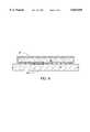
- the typical IC 10has lead frame leads 12, a die paddle 14, a semiconductor die 16 having a front side with circuitry and a back side, bond wires 18, and encapsulation material or other packaging layer 20.
- Bond wires 18attach to bond pads (not shown) on the front of the die 16. Bond wires provide the connection between the die and the lead frame leads.
- the leadsare attached to printed circuit boards (PCBs) or other devices (not shown).
- DIPdual in-line package
- TOPsthin small outline packages
- TABtape automated bonding
- COBchip-on-board
- COB assembly processestypically include the steps of bonding a die to a substrate and interconnecting the die to the substrate, using either conventional wire bond or TAB methods.
- TAB technologyhas eliminated the lead frame leads 12 and paddle 14, and instead uses TAB tape.
- TAB tapescomprise a predesigned network of electrical lines and buses which are attached to an IC die.
- the use of TAB tape and the elimination of lead framessave on fabrication steps and costs.
- the dieis connected to the TAB tape by a thermocompression or thermosonic bonder.
- the prior processeshave various disadvantages. Specifically, the testing of IC chips occurs after the TAB tape is attached to a number of die and to the substrate. Thus, when reliability testing takes place, any defective die requires replacement which increases costs. Additionally, by using these processes, several steps occur while the die is unprotected or not encapsulated which can result in additional die defects from increased exposure to the environment.
- a semiconductor device and method for forming the device which reduces the problems described abovewould be desirable.
- a semiconductor packaging techniqueis disclosed which is cost effective, reliable, and allows for testing of an IC die before it is mounted to TAB tape or soldered to a PC board.
- a semiconductor packaging techniqueis disclosed which is cost effective, reliable, and allows for testing of an IC die before it is mounted to TAB tape or soldered to a PC board.
- Uniquely, several layers of bonded beadsare formed and stacked higher than a total IC covering.
- FIG. 1is a cross section depicting a dual in-line package (DIP) semiconductor device.
- DIPdual in-line package
- FIGS. 2 through 5are cross sections illustrating process steps used with the inventive process.
- FIG. 6illustrates the bonding of ball bonded IC die to an electrical substrate providing electrical connection to other devices.
- FIGS. 7-8depict cross sections of an embodiment comprising wires for connection to bond pads.
- FIG. 9is a cross section showing the wires of FIG. 7 which have been flamed back (heated) to form raised contacts.
- FIGS. 10-13show embodiments having channels within a wafer section.
- U.S. Pat. No. 4,899,107is a discrete die burn-in for unpackaged die having same assignee as the present invention.
- FIG. 2is a detailed illustration of a first fabrication process of the invention, and includes the following elements: IC die 30, and gold ball towers 32. Discrete conductive elements other than the conductive balls shown are possible, such as conductive blocks or the wires as later described.
- first processthere are two steps. First, a completed IC die is manufactured and second, gold balls are welded in a tower fashion onto each bond pad of the die.
- the ballsmay be formed by other means from other materials such as solder wire or other conductive materials.
- the second main fabrication processis illustrated in FIG. 3.
- the gold ball tower bonded dieis placed into a cavity of a cavity bar holder or other holder 34 and onto a first layer of encapsulation material 36A.
- the encapsulating materialfunctions as a cushion between the die and holder 34, thus reducing damage.
- the encapsulating materialmay have any desired thickness on the faces of the die except, in this embodiment, for the side having the towers. The thickness of the encapsulating material on the tower side of the die is less than the height of the towers and allows for subsequent welding steps. Additionally, most any commonly known encapsulant material will suffice, such as siloxane polyimide etc.
- FIG. 4A third main fabrication process is illustrated in FIG. 4.
- a second layer of encapsulation material 36Bis applied over the tower side of the die.
- the die surfaceis covered while the towers are partially submerged in the material.
- a portion of the towersare not submerged in the material.
- the encapsulantfills a volume not occupied by encapsulation material 36A resulting in an encapsulated IC die as illustrated in FIG. 5 after the encapsulated device 40 is removed from the holder 34.
- towers 32function as leads. Therefore, the IC 40 can be tested for reliability and other factors before being mounted to tab tape or a PC board 50 as illustrated in FIG. 6. Additionally, IC contamination at later steps is reduced since the encapsulating process is completed.
- the ball bonded materialmay be any suitable welding material, such as compositions comprising aluminum, palladium, or other suitable materials.
- the encapsulationcan comprise many types of known materials suitable for that purpose, such as siloxane polyimide and epoxy novolac based materials.
- the ball bonded diecan also be clipped into a type of receptacle or socket, thus enabling easier removal for faster replacement of parts.
- FIGS. 7 and 8are cross sections showing another embodiment of the invention.
- a semiconductor die 30which has a plurality of bond pads (not shown) thereon with a wire 70 such as a ball bond formed from bond wire and electrically coupled with each pad.
- the dieis placed in a cavity bar holder 34 or other holder.
- no first layer of encapsulationis placed in the holder, although a first layer to cover the bottom of the holder can be formed as with previous embodiments to completely encapsulate the die 30.
- the wirecomprises a protruding portion 72 which protrudes from the encapsulation material 36 as shown.
- a vacuumcan be placed on a hole 74 through the holder 34 which secures the die to the holder. An embodiment using the vacuum hole may reduce movement of the die as the encapsulation is being formed in the cavity.
- a layer of encapsulation 36is formed within the cavity to cover the die 30 and a portion of the bond wire 70. Either before or after the die has been removed from the cavity, at least a portion, or preferably all of the protruding portion of each bond wire is removed such that the bond wire is exposed at the surface of the encapsulated device. Contact can then be made to some or all of the exposed portions of the bond wires.
- FIG. 9shows another embodiment of the invention.
- the structure of FIG. 7is formed as described above, and the protruding portions are trimmed (if necessary) and heated.
- the heat exposuremelts at least a portion of the exposed protruding bond wire and results in a raised contact or bump 90 which forms proximate the layer of encapsulation as shown. Contact can then be made to some or all of the raised contacts.
- the back of the semiconductor dieis exposed. Leaving the back of the die exposed may simplify the manufacturing process as forming two layers of encapsulation (one before placing the die in the cavity and one after) may be eliminated. Leaving the back of the die exposed would create no difficulties in many uses of the invention as the corner near the bond pads is covered by encapsulation. Also, a holder having sloped walls may aid in the removal of the encapsulated device. For example, a slope of about 10° or less would assist in the device removal while not excessively altering the outline of the package.
- FIGS. 10-12show another inventive embodiment of the invention.
- conductive balls 100such as those described in FIGS. 2-6 are shown with one or more ball on each bond pad, although an embodiment having the wires as described with FIGS. 7-9 would also be sufficient.
- a wafer section 102such as a part of a wafer or an entire wafer is provided which comprises a plurality of semiconductor die 104 with a channel 106 formed between the die 104.
- the channelscan be formed chemically by etching the die, mechanically such as by abrasive dicing, or by any workable means.
- the wafer sectionis placed in the holder 108, then encapsulation 110 is formed within the cavity and over the wafer section and conductive balls.
- the conductive ballscan be completely covered as shown, or the encapsulation can be formed to cover the wafer section and leave a portion of the conductive balls exposed. If the conductive balls are completely covered, they are exposed by removing a portion of the encapsulation such as shown in FIG. 11.
- the encapsulationcan be removed by laser ablation, chemical or mechanical means, or by other workable means. The entire surface can be planarized or a local removal of the encapsulation proximate the bond pads is also possible. Embodiments are also feasible wherein the encapsulation is not removed and contact is made to the conductive balls by a conductive probe which pierces the encapsulation.
- the dieAfter forming the encapsulation within the cavity and the channels, the die are segmented at the channels to result in the individual die packages 112 as shown in FIG. 12.
- the diecan be segmented at the channels by mechanically or chemically abrading the encapsulation which surrounds the die and the semiconductor material which forms the die.
- the dieare segmented using a saw blade of thickness less than the channel widths so as to leave encapsulation material for protecting the upper peripheral edges of the die.
- FIG. 13shows an embodiment similar to the embodiment of FIGS. 10-12 wherein a plurality of conductive balls 130 are formed on each bond pad and the encapsulation leaves at least a portion of one ball exposed. Removal of encapsulation to expose the ball is not required with this embodiment.
- a semiconductor device formed in accordance with the inventioncould conceivably be attached along with other devices to a printed circuit board, for example to a computer motherboard or as a part of a memory module used in a personal computer, a minicomputer, or a mainframe.
- the inventive deviceis useful in electronic devices related to telecommunications, the automobile industry, semiconductor test and manufacturing equipment, consumer electronics, or virtually any piece of consumer or industrial electronic equipment.
Landscapes
- Engineering & Computer Science (AREA)
- Computer Hardware Design (AREA)
- Microelectronics & Electronic Packaging (AREA)
- Power Engineering (AREA)
- Physics & Mathematics (AREA)
- Condensed Matter Physics & Semiconductors (AREA)
- General Physics & Mathematics (AREA)
- Manufacturing & Machinery (AREA)
- Encapsulation Of And Coatings For Semiconductor Or Solid State Devices (AREA)
- Wire Bonding (AREA)
Abstract
Description
This is a continuation-in-part of application Ser. No. 08/225,196, filed Apr. 8, 1994, now U.S. Pat. No. 5,496,775, which was a continuation of application Ser. No. 07/914,275, filed Jul. 15, 1992, now abandoned.
This invention relates to the field of integrated circuits and more particularly to a method for fabricating and packaging an integrated circuit device.
Historically, integrated circuits (ICs) have comprised a semiconductor die supported by a conductive lead frame. As illustrated in FIG. 1, thetypical IC 10 has lead frame leads 12, adie paddle 14, a semiconductor die 16 having a front side with circuitry and a back side,bond wires 18, and encapsulation material orother packaging layer 20.Bond wires 18 attach to bond pads (not shown) on the front of the die 16. Bond wires provide the connection between the die and the lead frame leads. The leads are attached to printed circuit boards (PCBs) or other devices (not shown).
The semiconductor industry pursues cost effective and reliable methods to decrease the size of semiconductor packages. The development of the dual in-line package (DIP) has been instrumental in the development of thin small outline packages (TSOPs), tape automated bonding (TAB), and chip-on-board (COB) technologies.
COB assembly processes typically include the steps of bonding a die to a substrate and interconnecting the die to the substrate, using either conventional wire bond or TAB methods.
In reference to FIG. 1, TAB technology has eliminated the lead frame leads 12 andpaddle 14, and instead uses TAB tape. TAB tapes comprise a predesigned network of electrical lines and buses which are attached to an IC die. The use of TAB tape and the elimination of lead frames save on fabrication steps and costs. Typically, the die is connected to the TAB tape by a thermocompression or thermosonic bonder.
The prior processes have various disadvantages. Specifically, the testing of IC chips occurs after the TAB tape is attached to a number of die and to the substrate. Thus, when reliability testing takes place, any defective die requires replacement which increases costs. Additionally, by using these processes, several steps occur while the die is unprotected or not encapsulated which can result in additional die defects from increased exposure to the environment.
A semiconductor device and method for forming the device which reduces the problems described above would be desirable.
One skilled in the art will appreciate the advantage of the subject IC and fabrication method for attaching an encapsulated and tested IC die to a PC board. Specifically, a semiconductor packaging technique is disclosed which is cost effective, reliable, and allows for testing of an IC die before it is mounted to TAB tape or soldered to a PC board. Uniquely, several layers of bonded beads are formed and stacked higher than a total IC covering.
Features of the present invention will become apparent from the following detailed description of the illustrated embodiments taken in conjunction with the accompanying drawings.
FIG. 1 is a cross section depicting a dual in-line package (DIP) semiconductor device.
FIGS. 2 through 5 are cross sections illustrating process steps used with the inventive process.
FIG. 6 illustrates the bonding of ball bonded IC die to an electrical substrate providing electrical connection to other devices.
FIGS. 7-8 depict cross sections of an embodiment comprising wires for connection to bond pads.
FIG. 9 is a cross section showing the wires of FIG. 7 which have been flamed back (heated) to form raised contacts.
FIGS. 10-13 show embodiments having channels within a wafer section.
It is noted that the illustrated embodiments are not drawn to scale, and they are only generally representative of the features of the invention.
The following U.S. patent is herein incorporated by reference: U.S. Pat. No. 4,899,107 is a discrete die burn-in for unpackaged die having same assignee as the present invention.
The following materials are incorporated by reference herein: Tape Automated Bonding Standardization and Implementation Requirements (Proposal), July, 1983, from the Solid State Products Engineering Council, 2001 Eye Street, NW, Washington D.C. 20006. Shindo TAB, a sales brochure for TAB tape, Toray Marketing & Sales (America), Inc., 1875 South Grant St., Suite 720, San Mateo, Calif. 94402.
FIG. 2 is a detailed illustration of a first fabrication process of the invention, and includes the following elements: IC die 30, andgold ball towers 32. Discrete conductive elements other than the conductive balls shown are possible, such as conductive blocks or the wires as later described.
In this first process there are two steps. First, a completed IC die is manufactured and second, gold balls are welded in a tower fashion onto each bond pad of the die. The balls may be formed by other means from other materials such as solder wire or other conductive materials.
One skilled in the art will recognize that there are many methods of creating a tower of gold material welding beads or balls. Moreover, 5 mil (1 mil=0.001 inches) wire is widely available which, after welding, will result in a ball having a diameter of about 15 mil. During the welding process the ball will decrease in height to about 1/2 to 2/3 of the diameter. It is noted that any size of gold bond wire may be used to comply with design constraints, and thus other sized balls may be similarly manufactured. Towers may be placed on any side of the die or on several sides of the die. Additionally, the gold material suggested may vary to other applicable materials or percentage of materials known for IC welding purposes. Finally, the height of the tower will vary depending upon the size of each ball and the number of balls used in the tower, for example up to 20 mils or higher. In this embodiment, it is desirable that the tower be higher than the encapsulating material.
The second main fabrication process is illustrated in FIG. 3. As shown in FIG. 3, the gold ball tower bonded die is placed into a cavity of a cavity bar holder orother holder 34 and onto a first layer ofencapsulation material 36A.
One skilled in the art will recognize that the gold towers are exposed and facing upwards. Moreover, the encapsulating material functions as a cushion between the die andholder 34, thus reducing damage. The encapsulating material may have any desired thickness on the faces of the die except, in this embodiment, for the side having the towers. The thickness of the encapsulating material on the tower side of the die is less than the height of the towers and allows for subsequent welding steps. Additionally, most any commonly known encapsulant material will suffice, such as siloxane polyimide etc.
A third main fabrication process is illustrated in FIG. 4. In this step a second layer ofencapsulation material 36B is applied over the tower side of the die. Thereby, the die surface is covered while the towers are partially submerged in the material. However, it is noted that a portion of the towers are not submerged in the material. The encapsulant fills a volume not occupied byencapsulation material 36A resulting in an encapsulated IC die as illustrated in FIG. 5 after the encapsulateddevice 40 is removed from theholder 34.
One skilled in the IC fabrication art will recognize thattowers 32 function as leads. Therefore, theIC 40 can be tested for reliability and other factors before being mounted to tab tape or aPC board 50 as illustrated in FIG. 6. Additionally, IC contamination at later steps is reduced since the encapsulating process is completed.
One skilled in the art will recognize that there are many variations to the illustrated embodiment. The ball bonded material may be any suitable welding material, such as compositions comprising aluminum, palladium, or other suitable materials.
The encapsulation can comprise many types of known materials suitable for that purpose, such as siloxane polyimide and epoxy novolac based materials.
There are several methods of attaching the completed ball bonded die onto a substrate. It is possible to weld the ball tower to the substrate. The ball bonded die can also be clipped into a type of receptacle or socket, thus enabling easier removal for faster replacement of parts.
FIGS. 7 and 8 are cross sections showing another embodiment of the invention. In this inventive method for forming a semiconductor device, and the structure which results therefrom, asemiconductor die 30 is provided which has a plurality of bond pads (not shown) thereon with awire 70 such as a ball bond formed from bond wire and electrically coupled with each pad. The die is placed in acavity bar holder 34 or other holder. In this embodiment, no first layer of encapsulation is placed in the holder, although a first layer to cover the bottom of the holder can be formed as with previous embodiments to completely encapsulate thedie 30. The wire comprises a protrudingportion 72 which protrudes from theencapsulation material 36 as shown. In an alternate embodiment, a vacuum can be placed on ahole 74 through theholder 34 which secures the die to the holder. An embodiment using the vacuum hole may reduce movement of the die as the encapsulation is being formed in the cavity.
After the die is placed within the cavity of the holder, a layer ofencapsulation 36 is formed within the cavity to cover thedie 30 and a portion of thebond wire 70. Either before or after the die has been removed from the cavity, at least a portion, or preferably all of the protruding portion of each bond wire is removed such that the bond wire is exposed at the surface of the encapsulated device. Contact can then be made to some or all of the exposed portions of the bond wires.
FIG. 9 shows another embodiment of the invention. In this embodiment, the structure of FIG. 7 is formed as described above, and the protruding portions are trimmed (if necessary) and heated. The heat exposure melts at least a portion of the exposed protruding bond wire and results in a raised contact or bump 90 which forms proximate the layer of encapsulation as shown. Contact can then be made to some or all of the raised contacts.
In the embodiments of FIGS. 7-9 the back of the semiconductor die is exposed. Leaving the back of the die exposed may simplify the manufacturing process as forming two layers of encapsulation (one before placing the die in the cavity and one after) may be eliminated. Leaving the back of the die exposed would create no difficulties in many uses of the invention as the corner near the bond pads is covered by encapsulation. Also, a holder having sloped walls may aid in the removal of the encapsulated device. For example, a slope of about 10° or less would assist in the device removal while not excessively altering the outline of the package.
FIGS. 10-12 show another inventive embodiment of the invention. In this embodiment,conductive balls 100 such as those described in FIGS. 2-6 are shown with one or more ball on each bond pad, although an embodiment having the wires as described with FIGS. 7-9 would also be sufficient. In the embodiment of FIGS. 10-12 awafer section 102 such as a part of a wafer or an entire wafer is provided which comprises a plurality of semiconductor die 104 with achannel 106 formed between the die 104. The channels can be formed chemically by etching the die, mechanically such as by abrasive dicing, or by any workable means. The wafer section is placed in theholder 108, then encapsulation 110 is formed within the cavity and over the wafer section and conductive balls. The conductive balls can be completely covered as shown, or the encapsulation can be formed to cover the wafer section and leave a portion of the conductive balls exposed. If the conductive balls are completely covered, they are exposed by removing a portion of the encapsulation such as shown in FIG. 11. The encapsulation can be removed by laser ablation, chemical or mechanical means, or by other workable means. The entire surface can be planarized or a local removal of the encapsulation proximate the bond pads is also possible. Embodiments are also feasible wherein the encapsulation is not removed and contact is made to the conductive balls by a conductive probe which pierces the encapsulation.
After forming the encapsulation within the cavity and the channels, the die are segmented at the channels to result in theindividual die packages 112 as shown in FIG. 12. The die can be segmented at the channels by mechanically or chemically abrading the encapsulation which surrounds the die and the semiconductor material which forms the die. In one exemplary preferred embodiment, the die are segmented using a saw blade of thickness less than the channel widths so as to leave encapsulation material for protecting the upper peripheral edges of the die.
FIG. 13 shows an embodiment similar to the embodiment of FIGS. 10-12 wherein a plurality ofconductive balls 130 are formed on each bond pad and the encapsulation leaves at least a portion of one ball exposed. Removal of encapsulation to expose the ball is not required with this embodiment.
A semiconductor device formed in accordance with the invention could conceivably be attached along with other devices to a printed circuit board, for example to a computer motherboard or as a part of a memory module used in a personal computer, a minicomputer, or a mainframe. An assembly similar to that described in U.S. Pat. No. 5,360,992 to Lowrey, et al. which is assigned to Micron Technology, Inc. and incorporated herein by reference, is also feasible with the inventive structure described herein. The inventive device is useful in electronic devices related to telecommunications, the automobile industry, semiconductor test and manufacturing equipment, consumer electronics, or virtually any piece of consumer or industrial electronic equipment.
While the invention has been taught with specific reference to one embodiment, one skilled in the art will recognize that changes can be made in form and detail without departing from the spirit and the scope of the invention. For example, instead of gravity leveling the encapsulation it may be possible to spin coat the die (or wafer or wafer section) with encapsulation to optimize the thickness of the encapsulation.
Claims (20)
1. A method for forming a semiconductor device comprising the following steps:
providing a semiconductor die having a plurality of pads thereon with at least one discrete conductive element on at least one of said pads;
providing a holder having a cavity therein;
placing said semiconductor die in said cavity;
subsequent to placing said die within said cavity, forming a layer of encapsulation material within said cavity thereby covering said die with said encapsulation material; and
subsequent to forming said layer of encapsulation, removing said encapsulated die from said cavity.
2. The method of claim 1, wherein a plurality of discrete conductive elements are formed over at least one of said pads.
3. The method of claim 1 further comprising the steps of:
completely covering said discrete conductive element with said encapsulation;
removing a portion of said encapsulation to expose at least a portion of said discrete conductive element.
4. The method of claim 1 further comprising the step of placing said die on said holder during said step of placing said semiconductor die in said cavity.
5. The method of claim 4 wherein a portion of said die remains exposed after said step of removing said encapsulated die from said cavity.
6. The method of claim 1 wherein said layer of encapsulation is a second layer of encapsulation, further comprising the steps of:
forming a first layer of encapsulation within said cavity prior to said step of placing said die in said cavity;
placing said die on said first layer of encapsulation during said step of placing said die in said cavity.
7. A method of forming a semiconductor device, comprising:
providing a wafer section comprising a plurality of semiconductor die each having a plurality of pads thereon, with at least one conductive ball on at least one of said pads of each of said die;
placing said wafer section in said cavity;
subsequent to placing said wafer section within said cavity, forming a layer of encapsulation material within said cavity thereby covering said wafer section with said encapsulation material; and
subsequent to forming said layer of encapsulation, removing said encapsulated wafer section from said cavity.
8. The method of claim 7 wherein said wafer section comprises a semiconductor wafer.
9. The method of claim 7 further comprising the steps of:
completely covering said conductive balls with said encapsulation;
removing a portion of said encapsulation to expose at least a portion of said conductive balls.
10. The method of claim 7 further comprising the step of placing said plurality of die on said holder during said step of placing said semiconductor die in said cavity.
11. The method of claim 10 wherein said plurality of die remain exposed after said step of removing said encapsulated die from said cavity.
12. The method of claim 7 wherein said layer of encapsulation is a second layer of encapsulation, further comprising the steps of:
forming a first layer of encapsulation within said cavity prior to said step of placing said wafer section in said cavity;
placing said wafer section on said first layer of encapsulation during said step of placing said wafer section in said cavity.
13. The method of claim 7 further comprising the following steps:
forming a channel between said die;
forming encapsulation material within said channel;
subsequent to forming said encapsulation within said channel, segmenting said die at said channel.
14. A method for forming a semiconductor device comprising the following steps:
providing a semiconductor die having a plurality of pads thereon with at least one bond wire electrically coupled with one of said pads;
providing a holder having a cavity therein;
placing said semiconductor die in said cavity;
subsequent to placing said die within said cavity, forming a layer of encapsulation material within said cavity thereby covering said die with said encapsulation material; and
subsequent to forming said layer of encapsulation, removing the encapsulated die from said cavity.
15. The method of claim 14 wherein said bond wire comprises a protruding portion which protrudes from said encapsulation material subsequent to said step of forming said layer of encapsulation material, further comprising the step of removing at least part of said protruding portion of said bond wire.
16. The method of claim 14 wherein said bond wire comprises a protruding portion which protrudes from said encapsulation material subsequent to said step of forming said layer of encapsulation material, further comprising the step of heating said protruding portion of said bond wire so as to form a raised contact proximate said layer of encapsulation.
17. The method of claim 14 wherein said die is one of a plurality of unsegmented semiconductor die each having a plurality of bond pads thereon, said plurality of die forming a wafer section, further comprising the following steps:
providing at least one bond wire electrically coupled with one of said pads of each of said die;
placing said wafer section in said cavity;
during said step of forming a layer of encapsulation material within said cavity, covering said wafer section with said encapsulation material.
18. The method of claim 17 further comprising the following steps:
forming a channel between said die;
forming encapsulation material within said channel;
subsequent to forming said encapsulation within said channel, segmenting said die at said channel.
19. The method of claim 18 wherein said each said bond wire comprises a protruding portion which protrudes from said encapsulation material subsequent to said step of forming said layer of encapsulation material, further comprising the step of removing at least part of said protruding portion of each said bond wire.
20. The method of claim 18 wherein each said bond wire comprises a protruding portion which protrudes from said encapsulation material subsequent to said step of forming said layer of encapsulation material, further comprising the step of heating each said protruding portion of each said bond wire such that said each protruding portion forms a raised contact proximate said layer of encapsulation.
Priority Applications (3)
| Application Number | Priority Date | Filing Date | Title |
|---|---|---|---|
| US08/611,314US5824569A (en) | 1992-07-15 | 1996-03-05 | Semiconductor device having ball-bonded pads |
| US09/175,807US6043564A (en) | 1992-07-15 | 1998-10-20 | Semiconductor device having ball-bonded pads |
| US09/536,965US6362532B1 (en) | 1992-07-15 | 2000-03-28 | Semiconductor device having ball-bonded pads |
Applications Claiming Priority (3)
| Application Number | Priority Date | Filing Date | Title |
|---|---|---|---|
| US91427592A | 1992-07-15 | 1992-07-15 | |
| US08/225,196US5496775A (en) | 1992-07-15 | 1994-04-08 | Semiconductor device having ball-bonded pads |
| US08/611,314US5824569A (en) | 1992-07-15 | 1996-03-05 | Semiconductor device having ball-bonded pads |
Related Parent Applications (1)
| Application Number | Title | Priority Date | Filing Date |
|---|---|---|---|
| US08/225,196Continuation-In-PartUS5496775A (en) | 1992-07-15 | 1994-04-08 | Semiconductor device having ball-bonded pads |
Related Child Applications (1)
| Application Number | Title | Priority Date | Filing Date |
|---|---|---|---|
| US09/175,807ContinuationUS6043564A (en) | 1992-07-15 | 1998-10-20 | Semiconductor device having ball-bonded pads |
Publications (1)
| Publication Number | Publication Date |
|---|---|
| US5824569Atrue US5824569A (en) | 1998-10-20 |
Family
ID=46251826
Family Applications (3)
| Application Number | Title | Priority Date | Filing Date |
|---|---|---|---|
| US08/611,314Expired - LifetimeUS5824569A (en) | 1992-07-15 | 1996-03-05 | Semiconductor device having ball-bonded pads |
| US09/175,807Expired - LifetimeUS6043564A (en) | 1992-07-15 | 1998-10-20 | Semiconductor device having ball-bonded pads |
| US09/536,965Expired - Fee RelatedUS6362532B1 (en) | 1992-07-15 | 2000-03-28 | Semiconductor device having ball-bonded pads |
Family Applications After (2)
| Application Number | Title | Priority Date | Filing Date |
|---|---|---|---|
| US09/175,807Expired - LifetimeUS6043564A (en) | 1992-07-15 | 1998-10-20 | Semiconductor device having ball-bonded pads |
| US09/536,965Expired - Fee RelatedUS6362532B1 (en) | 1992-07-15 | 2000-03-28 | Semiconductor device having ball-bonded pads |
Country Status (1)
| Country | Link |
|---|---|
| US (3) | US5824569A (en) |
Cited By (39)
| Publication number | Priority date | Publication date | Assignee | Title |
|---|---|---|---|---|
| US6182342B1 (en) | 1999-04-02 | 2001-02-06 | Andersen Laboratories, Inc. | Method of encapsulating a saw device |
| US6194250B1 (en)* | 1998-09-14 | 2001-02-27 | Motorola, Inc. | Low-profile microelectronic package |
| US6229209B1 (en) | 1995-02-23 | 2001-05-08 | Matsushita Electric Industrial Co., Ltd. | Chip carrier |
| US20010003049A1 (en)* | 1996-07-12 | 2001-06-07 | Norio Fukasawa | Method and mold for manufacturing semiconductor device, semiconductor device, and method for mounting the device |
| US6291894B1 (en)* | 1998-08-31 | 2001-09-18 | Micron Technology, Inc. | Method and apparatus for a semiconductor package for vertical surface mounting |
| US6335208B1 (en)* | 1999-05-10 | 2002-01-01 | Intersil Americas Inc. | Laser decapsulation method |
| WO2002058233A1 (en)* | 2001-01-18 | 2002-07-25 | Infineon Technologies Ag | Filter devices and method for fabricating filter devices |
| US20020142514A1 (en)* | 2001-03-28 | 2002-10-03 | Scheifers Steven M. | Microelectronic assembly with die support and method |
| US20020173070A1 (en)* | 2000-08-21 | 2002-11-21 | Bolken Todd O. | Method and apparatus for encapsulating a multi-chip substrate array |
| US20030089758A1 (en)* | 2000-12-22 | 2003-05-15 | Chun-Chi Lee | Wire bonding process and wire bond structure |
| US20030167630A1 (en)* | 2002-03-07 | 2003-09-11 | Pham Cuong Van | Method for attaching a die with a low melting metal |
| US20040043675A1 (en)* | 2002-08-29 | 2004-03-04 | Micron Technology, Inc. | Multi-component integrated circuit contacts |
| US20040046257A1 (en)* | 2002-09-06 | 2004-03-11 | Advanpack Solutions Pte.Ltd. | Package design and method of manufacture for chip grid array |
| US6709893B2 (en)* | 1998-05-11 | 2004-03-23 | Micron Technology, Inc. | Interconnections for a semiconductor device and method for forming same |
| US6717245B1 (en) | 2000-06-02 | 2004-04-06 | Micron Technology, Inc. | Chip scale packages performed by wafer level processing |
| US6777261B2 (en) | 2000-12-26 | 2004-08-17 | Micron Technology, Inc. | Method and apparatus for a semiconductor package for vertical surface mounting |
| US20040227259A1 (en)* | 1999-07-28 | 2004-11-18 | Seiko Epson Corporation | Substrate for semiconductor device, semiconductor chip mounting substrate, semiconductor device and method of fabrication thereof, and circuit board, together with electronic equipment |
| US20040238926A1 (en)* | 2003-03-20 | 2004-12-02 | Seiko Epson Corporation | Semiconductor wafer, semiconductor device and method for manufacturing same, circuit board, and electronic apparatus |
| US6881611B1 (en)* | 1996-07-12 | 2005-04-19 | Fujitsu Limited | Method and mold for manufacturing semiconductor device, semiconductor device and method for mounting the device |
| US20060192284A1 (en)* | 2003-09-26 | 2006-08-31 | Advanced Semiconductor Engineering, Inc. | Method of forming an encapsulation layer on a back side of a wafer |
| US7217999B1 (en)* | 1999-10-05 | 2007-05-15 | Nec Electronics Corporation | Multilayer interconnection board, semiconductor device having the same, and method of forming the same as well as method of mounting the semiconductor chip on the interconnection board |
| US20070158833A1 (en)* | 2006-01-04 | 2007-07-12 | Soo-San Park | Integrated circuit package system including stacked die |
| US20070158809A1 (en)* | 2006-01-04 | 2007-07-12 | Chow Seng G | Multi-chip package system |
| US20070182018A1 (en)* | 2006-02-09 | 2007-08-09 | Stats Chippac Ltd. | Integrated circuit package system including zero fillet resin |
| US20070190690A1 (en)* | 2006-02-14 | 2007-08-16 | Stats Chippac Ltd. | Integrated circuit package system with exposed interconnects |
| US20070202617A1 (en)* | 2005-04-08 | 2007-08-30 | Hembree David R | Method for fabricating stacked semiconductor components with through wire interconnects |
| US20070246819A1 (en)* | 2006-04-24 | 2007-10-25 | Micron Technology, Inc. | Semiconductor components and systems having encapsulated through wire interconnects (TWI) and wafer level methods of fabrication |
| US20080203549A1 (en)* | 2006-02-25 | 2008-08-28 | Seng Guan Chow | Stackable integrated circuit package system with multiple interconnect interface |
| US20080229573A1 (en)* | 2005-05-19 | 2008-09-25 | Wood Alan G | System For Fabricating Semiconductor Components With Conductive Interconnects |
| US7579267B2 (en) | 2005-12-07 | 2009-08-25 | Micron Technology, Inc. | Methods and systems for fabricating semiconductor components with through wire interconnects (TWI) |
| US7687315B2 (en) | 2005-04-29 | 2010-03-30 | Stats Chippac Ltd. | Stacked integrated circuit package system and method of manufacture therefor |
| US20100159645A1 (en)* | 1998-09-01 | 2010-06-24 | Sony Corporation | Semiconductor apparatus and process of production thereof |
| US7855100B2 (en) | 2005-03-31 | 2010-12-21 | Stats Chippac Ltd. | Integrated circuit package system with an encapsulant cavity and method of fabrication thereof |
| US20120032325A1 (en)* | 2005-10-03 | 2012-02-09 | Rohm Co., Ltd. | Semiconductor device |
| US20120181689A1 (en)* | 2008-12-08 | 2012-07-19 | Stats Chippac, Ltd. | Semiconductor Device and Method of Forming Bond Wires and Stud Bumps in Recessed Region of Peripheral Area around the Device for Electrical Interconnection to Other Devices |
| US20130037990A1 (en)* | 2011-08-11 | 2013-02-14 | Taiwan Semiconductor Manufacturing Company, Ltd. | Molding Wafer Chamber |
| TWI387062B (en)* | 2006-01-23 | 2013-02-21 | Digitaloptics Corp Europe Ltd | Wafer level packaging to lidded chips |
| US20140321063A1 (en)* | 2013-04-30 | 2014-10-30 | Infineon Technologies Ag | Directly Cooled Substrates for Semiconductor Modules and Corresponding Manufacturing Methods |
| US10522505B2 (en)* | 2017-04-06 | 2019-12-31 | Advanced Semiconductor Engineering, Inc. | Semiconductor device package and method for manufacturing the same |
Families Citing this family (11)
| Publication number | Priority date | Publication date | Assignee | Title |
|---|---|---|---|---|
| US5824569A (en)* | 1992-07-15 | 1998-10-20 | Micron Technology, Inc. | Semiconductor device having ball-bonded pads |
| DE10206661A1 (en)* | 2001-02-20 | 2002-09-26 | Infineon Technologies Ag | Electronic component used in semiconductors comprises a semiconductor chip surrounded by a sawn edge having profile-sawn contours of semiconductor material and surrounded by a plastic composition forming a plastic edge |
| US6686225B2 (en)* | 2001-07-27 | 2004-02-03 | Texas Instruments Incorporated | Method of separating semiconductor dies from a wafer |
| DE10156386B4 (en)* | 2001-11-16 | 2007-08-09 | Infineon Technologies Ag | Method for producing a semiconductor chip |
| US7122884B2 (en)* | 2002-04-16 | 2006-10-17 | Fairchild Semiconductor Corporation | Robust leaded molded packages and methods for forming the same |
| US8022489B2 (en)* | 2005-05-20 | 2011-09-20 | Macronix International Co., Ltd. | Air tunnel floating gate memory cell |
| US7589406B2 (en)* | 2005-06-27 | 2009-09-15 | Micron Technology, Inc. | Stacked semiconductor component |
| KR100871707B1 (en)* | 2007-03-30 | 2008-12-05 | 삼성전자주식회사 | Wafer level package having molding part to suppress cracking and manufacturing method thereof |
| US20080280393A1 (en)* | 2007-05-09 | 2008-11-13 | Taiwan Semiconductor Manufacturing Co., Ltd. | Methods for forming package structures |
| US20100089578A1 (en)* | 2008-10-10 | 2010-04-15 | Nguyen Philip D | Prevention of Water Intrusion Into Particulates |
| US8663220B2 (en)* | 2009-07-15 | 2014-03-04 | Ethicon Endo-Surgery, Inc. | Ultrasonic surgical instruments |
Citations (13)
| Publication number | Priority date | Publication date | Assignee | Title |
|---|---|---|---|---|
| US3212160A (en)* | 1962-05-18 | 1965-10-19 | Transitron Electronic Corp | Method of manufacturing semiconductive devices |
| US4600600A (en)* | 1983-11-30 | 1986-07-15 | Siemens Aktiengesellschaft | Method for the galvanic manufacture of metallic bump-like lead contacts |
| US4899107A (en)* | 1988-09-30 | 1990-02-06 | Micron Technology, Inc. | Discrete die burn-in for nonpackaged die |
| US5019535A (en)* | 1989-03-28 | 1991-05-28 | General Electric Company | Die attachment method using nonconductive adhesive for use in high density interconnected assemblies |
| US5071787A (en)* | 1989-03-14 | 1991-12-10 | Kabushiki Kaisha Toshiba | Semiconductor device utilizing a face-down bonding and a method for manufacturing the same |
| US5143865A (en)* | 1988-09-02 | 1992-09-01 | Kabushiki Kaisha Toshiba | Metal bump type semiconductor device and method for manufacturing the same |
| US5207585A (en)* | 1990-10-31 | 1993-05-04 | International Business Machines Corporation | Thin interface pellicle for dense arrays of electrical interconnects |
| US5225023A (en)* | 1989-02-21 | 1993-07-06 | General Electric Company | High density interconnect thermoplastic die attach material and solvent die attach processing |
| US5289346A (en)* | 1991-02-26 | 1994-02-22 | Microelectronics And Computer Technology Corporation | Peripheral to area adapter with protective bumper for an integrated circuit chip |
| US5341564A (en)* | 1992-03-24 | 1994-08-30 | Unisys Corporation | Method of fabricating integrated circuit module |
| US5496775A (en)* | 1992-07-15 | 1996-03-05 | Micron Semiconductor, Inc. | Semiconductor device having ball-bonded pads |
| US5567656A (en)* | 1993-12-27 | 1996-10-22 | Goldstar Electron Co., Ltd. | Process for packaging semiconductor device |
| US5663106A (en)* | 1994-05-19 | 1997-09-02 | Tessera, Inc. | Method of encapsulating die and chip carrier |
Family Cites Families (3)
| Publication number | Priority date | Publication date | Assignee | Title |
|---|---|---|---|---|
| US4807021A (en) | 1986-03-10 | 1989-02-21 | Kabushiki Kaisha Toshiba | Semiconductor device having stacking structure |
| US5824569A (en)* | 1992-07-15 | 1998-10-20 | Micron Technology, Inc. | Semiconductor device having ball-bonded pads |
| JP3258764B2 (en)* | 1993-06-01 | 2002-02-18 | 三菱電機株式会社 | Method for manufacturing resin-encapsulated semiconductor device, external lead-out electrode and method for manufacturing the same |
- 1996
- 1996-03-05USUS08/611,314patent/US5824569A/ennot_activeExpired - Lifetime
- 1998
- 1998-10-20USUS09/175,807patent/US6043564A/ennot_activeExpired - Lifetime
- 2000
- 2000-03-28USUS09/536,965patent/US6362532B1/ennot_activeExpired - Fee Related
Patent Citations (14)
| Publication number | Priority date | Publication date | Assignee | Title |
|---|---|---|---|---|
| US3212160A (en)* | 1962-05-18 | 1965-10-19 | Transitron Electronic Corp | Method of manufacturing semiconductive devices |
| US4600600A (en)* | 1983-11-30 | 1986-07-15 | Siemens Aktiengesellschaft | Method for the galvanic manufacture of metallic bump-like lead contacts |
| US5143865A (en)* | 1988-09-02 | 1992-09-01 | Kabushiki Kaisha Toshiba | Metal bump type semiconductor device and method for manufacturing the same |
| US4899107A (en)* | 1988-09-30 | 1990-02-06 | Micron Technology, Inc. | Discrete die burn-in for nonpackaged die |
| US5348607A (en)* | 1989-02-21 | 1994-09-20 | General Electric Company | High density interconnect thermoplastic die attach material and solvent die attach processing |
| US5225023A (en)* | 1989-02-21 | 1993-07-06 | General Electric Company | High density interconnect thermoplastic die attach material and solvent die attach processing |
| US5071787A (en)* | 1989-03-14 | 1991-12-10 | Kabushiki Kaisha Toshiba | Semiconductor device utilizing a face-down bonding and a method for manufacturing the same |
| US5019535A (en)* | 1989-03-28 | 1991-05-28 | General Electric Company | Die attachment method using nonconductive adhesive for use in high density interconnected assemblies |
| US5207585A (en)* | 1990-10-31 | 1993-05-04 | International Business Machines Corporation | Thin interface pellicle for dense arrays of electrical interconnects |
| US5289346A (en)* | 1991-02-26 | 1994-02-22 | Microelectronics And Computer Technology Corporation | Peripheral to area adapter with protective bumper for an integrated circuit chip |
| US5341564A (en)* | 1992-03-24 | 1994-08-30 | Unisys Corporation | Method of fabricating integrated circuit module |
| US5496775A (en)* | 1992-07-15 | 1996-03-05 | Micron Semiconductor, Inc. | Semiconductor device having ball-bonded pads |
| US5567656A (en)* | 1993-12-27 | 1996-10-22 | Goldstar Electron Co., Ltd. | Process for packaging semiconductor device |
| US5663106A (en)* | 1994-05-19 | 1997-09-02 | Tessera, Inc. | Method of encapsulating die and chip carrier |
Non-Patent Citations (3)
| Title |
|---|
| "Shindo TAB", a sales brochure for TAB tape, Toray Marketing & Sales (America), INC, 1875 S. Grant St., Ste. 720, San Mateo, CA. |
| Shindo TAB , a sales brochure for TAB tape, Toray Marketing & Sales (America), INC, 1875 S. Grant St., Ste. 720, San Mateo, CA.* |
| Tape Automated bonding Standardization and Implementation Requirements (Proposal), Jul. 1983, Solid State Products Engineering Council, 2001 Eye St., NW, Washington D.C.* |
Cited By (123)
| Publication number | Priority date | Publication date | Assignee | Title |
|---|---|---|---|---|
| US6229209B1 (en) | 1995-02-23 | 2001-05-08 | Matsushita Electric Industrial Co., Ltd. | Chip carrier |
| US6365499B1 (en) | 1995-02-23 | 2002-04-02 | Matsushita Electric Industrial Co., Ltd. | Chip carrier and method of manufacturing and mounting the same |
| US6372547B2 (en)* | 1995-02-23 | 2002-04-16 | Matsushita Electric Industrial Co., Ltd. | Method for manufacturing electronic device with resin layer between chip carrier and circuit wiring board |
| US20010003049A1 (en)* | 1996-07-12 | 2001-06-07 | Norio Fukasawa | Method and mold for manufacturing semiconductor device, semiconductor device, and method for mounting the device |
| US6881611B1 (en)* | 1996-07-12 | 2005-04-19 | Fujitsu Limited | Method and mold for manufacturing semiconductor device, semiconductor device and method for mounting the device |
| US20020030258A1 (en)* | 1996-07-12 | 2002-03-14 | Fujitsu Limited | Method and mold for manufacturing semiconductor device, semiconductor device, and method for mounting the device |
| US20040178512A1 (en)* | 1998-05-11 | 2004-09-16 | Moden Walter L. | Interconnections for a semiconductor device |
| US6709893B2 (en)* | 1998-05-11 | 2004-03-23 | Micron Technology, Inc. | Interconnections for a semiconductor device and method for forming same |
| US6974725B2 (en) | 1998-05-11 | 2005-12-13 | Micron Technology, Inc. | Interconnections for a semiconductor device |
| US6511863B2 (en) | 1998-08-31 | 2003-01-28 | Micron Technology, Inc. | Method and apparatus for a semiconductor package for vertical surface mounting |
| US6903465B2 (en) | 1998-08-31 | 2005-06-07 | Micron Technology, Inc. | Method and apparatus for a semiconductor package for vertical surface mounting |
| US6291894B1 (en)* | 1998-08-31 | 2001-09-18 | Micron Technology, Inc. | Method and apparatus for a semiconductor package for vertical surface mounting |
| US20100159645A1 (en)* | 1998-09-01 | 2010-06-24 | Sony Corporation | Semiconductor apparatus and process of production thereof |
| US6194250B1 (en)* | 1998-09-14 | 2001-02-27 | Motorola, Inc. | Low-profile microelectronic package |
| US6182342B1 (en) | 1999-04-02 | 2001-02-06 | Andersen Laboratories, Inc. | Method of encapsulating a saw device |
| USRE43980E1 (en) | 1999-05-10 | 2013-02-05 | Intersil Corporation | Laser decapsulation method |
| US7166186B2 (en) | 1999-05-10 | 2007-01-23 | Intersil Americas Inc. | Laser decapsulation apparatus and method |
| US7316936B2 (en) | 1999-05-10 | 2008-01-08 | Intersil Americans Inc. | Laser decapsulation method |
| US6335208B1 (en)* | 1999-05-10 | 2002-01-01 | Intersil Americas Inc. | Laser decapsulation method |
| USRE42193E1 (en) | 1999-05-10 | 2011-03-01 | Intersil Corporation | Laser decapsulation method |
| US20070111337A1 (en)* | 1999-05-10 | 2007-05-17 | Lowry Robert K | Laser decapsulation apparatus and method |
| US20040227259A1 (en)* | 1999-07-28 | 2004-11-18 | Seiko Epson Corporation | Substrate for semiconductor device, semiconductor chip mounting substrate, semiconductor device and method of fabrication thereof, and circuit board, together with electronic equipment |
| US8008130B2 (en) | 1999-10-05 | 2011-08-30 | Renesas Electronics Corporation | Multilayer interconnection board, semiconductor device having the same, and method of forming the same as well as method of mounting the semicondutor chip on the interconnection board |
| US7217999B1 (en)* | 1999-10-05 | 2007-05-15 | Nec Electronics Corporation | Multilayer interconnection board, semiconductor device having the same, and method of forming the same as well as method of mounting the semiconductor chip on the interconnection board |
| US6900079B2 (en) | 2000-06-02 | 2005-05-31 | Micron Technology, Inc. | Method for fabricating a chip scale package using wafer level processing |
| US7183191B2 (en) | 2000-06-02 | 2007-02-27 | Micron Technology, Inc. | Method for fabricating a chip scale package using wafer level processing |
| US6780746B2 (en)* | 2000-06-02 | 2004-08-24 | Micron Technology, Inc. | Method for fabricating a chip scale package using wafer level processing and devices resulting therefrom |
| US20040126928A1 (en)* | 2000-06-02 | 2004-07-01 | Kinsman Larry D. | Method for fabricating a chip scale package using wafer level processing and devices resulting therefrom |
| US7727858B2 (en) | 2000-06-02 | 2010-06-01 | Micron Technology, Inc. | Method for fabricating a chip scale package using wafer level processing |
| US6717245B1 (en) | 2000-06-02 | 2004-04-06 | Micron Technology, Inc. | Chip scale packages performed by wafer level processing |
| US20050164429A1 (en)* | 2000-06-02 | 2005-07-28 | Kinsman Larry D. | Method for fabricating a chip scale package using wafer level processing |
| US20070148918A1 (en)* | 2000-06-02 | 2007-06-28 | Kinsman Larry D | Method for fabricating a chip scale package using wafer level processing |
| US7156633B2 (en) | 2000-08-21 | 2007-01-02 | Micron Technology, Inc. | Apparatus for encapsulating a multi-chip substrate array |
| US6576496B1 (en)* | 2000-08-21 | 2003-06-10 | Micron Technology, Inc. | Method and apparatus for encapsulating a multi-chip substrate array |
| US6910874B2 (en) | 2000-08-21 | 2005-06-28 | Micron Technology, Inc. | Apparatus for encapsulating a multi-chip substrate array |
| US6746895B2 (en) | 2000-08-21 | 2004-06-08 | Micron Technology, Inc. | Method for encapsulating a multi-chip substrate array |
| US20050189642A1 (en)* | 2000-08-21 | 2005-09-01 | Bolken Todd O. | Apparatus for encapsulating a multi-chip substrate array |
| US20020173070A1 (en)* | 2000-08-21 | 2002-11-21 | Bolken Todd O. | Method and apparatus for encapsulating a multi-chip substrate array |
| US6863208B2 (en)* | 2000-12-22 | 2005-03-08 | Advanced Semiconductor Enigneering, Inc. | Wire bonding process and wire bond structure |
| US20030089758A1 (en)* | 2000-12-22 | 2003-05-15 | Chun-Chi Lee | Wire bonding process and wire bond structure |
| US6777261B2 (en) | 2000-12-26 | 2004-08-17 | Micron Technology, Inc. | Method and apparatus for a semiconductor package for vertical surface mounting |
| US20040029356A1 (en)* | 2001-01-18 | 2004-02-12 | Hans-Jorg Timme | Filter device and method for fabricating filter devices |
| US7291547B2 (en) | 2001-01-18 | 2007-11-06 | Infineon Technologies A.G. | Filter device and method for fabricating filter devices |
| WO2002058233A1 (en)* | 2001-01-18 | 2002-07-25 | Infineon Technologies Ag | Filter devices and method for fabricating filter devices |
| US6562663B2 (en)* | 2001-03-28 | 2003-05-13 | Motorola, Inc. | Microelectronic assembly with die support and method |
| US20040002181A1 (en)* | 2001-03-28 | 2004-01-01 | Scheifers Steven M. | Microelectronic assembly with die support and method |
| US20020142514A1 (en)* | 2001-03-28 | 2002-10-03 | Scheifers Steven M. | Microelectronic assembly with die support and method |
| US6826829B2 (en)* | 2002-03-07 | 2004-12-07 | Visteon Global Technologies, Inc. | Method for attaching a die with a low melting metal |
| US20030167630A1 (en)* | 2002-03-07 | 2003-09-11 | Pham Cuong Van | Method for attaching a die with a low melting metal |
| US20060001141A1 (en)* | 2002-08-29 | 2006-01-05 | Micron Technology, Inc. | Multi-component integrated circuit contacts |
| US7115998B2 (en) | 2002-08-29 | 2006-10-03 | Micron Technology, Inc. | Multi-component integrated circuit contacts |
| US20100203721A1 (en)* | 2002-08-29 | 2010-08-12 | Hiatt William M | Multi-component integrated circuit contacts |
| US9337162B2 (en) | 2002-08-29 | 2016-05-10 | Micron Technology, Inc. | Multi-component integrated circuit contacts |
| US20040043675A1 (en)* | 2002-08-29 | 2004-03-04 | Micron Technology, Inc. | Multi-component integrated circuit contacts |
| US7719120B2 (en) | 2002-08-29 | 2010-05-18 | Micron Technology, Inc. | Multi-component integrated circuit contacts |
| US8268715B2 (en) | 2002-08-29 | 2012-09-18 | Micron Technology, Inc. | Multi-component integrated circuit contacts |
| US20070018321A1 (en)* | 2002-08-29 | 2007-01-25 | Micron Technology, Inc. | Multi-component integrated circuit contacts |
| US7446028B2 (en) | 2002-08-29 | 2008-11-04 | Micron Technology, Inc. | Multi-component integrated circuit contacts |
| US6929981B2 (en)* | 2002-09-06 | 2005-08-16 | Advanpack Solutions Pte, Ltd. | Package design and method of manufacture for chip grid array |
| US7456496B2 (en) | 2002-09-06 | 2008-11-25 | Advanpack Solutions Pte Ltd | Package design and method of manufacture for chip grid array |
| US20050205987A1 (en)* | 2002-09-06 | 2005-09-22 | Advanpack Solutions Pte. Ltd. | Package design and method of manufacture for chip grid array |
| US20040046257A1 (en)* | 2002-09-06 | 2004-03-11 | Advanpack Solutions Pte.Ltd. | Package design and method of manufacture for chip grid array |
| US20040238926A1 (en)* | 2003-03-20 | 2004-12-02 | Seiko Epson Corporation | Semiconductor wafer, semiconductor device and method for manufacturing same, circuit board, and electronic apparatus |
| US20060192284A1 (en)* | 2003-09-26 | 2006-08-31 | Advanced Semiconductor Engineering, Inc. | Method of forming an encapsulation layer on a back side of a wafer |
| US8309397B2 (en) | 2005-03-31 | 2012-11-13 | Stats Chippac Ltd. | Integrated circuit packaging system with a component in an encapsulant cavity and method of fabrication thereof |
| US8021924B2 (en) | 2005-03-31 | 2011-09-20 | Stats Chippac Ltd. | Encapsulant cavity integrated circuit package system and method of fabrication thereof |
| US20110018084A1 (en)* | 2005-03-31 | 2011-01-27 | Il Kwon Shim | Encapsulant cavity integrated circuit package system and method of fabrication thereof |
| US7855100B2 (en) | 2005-03-31 | 2010-12-21 | Stats Chippac Ltd. | Integrated circuit package system with an encapsulant cavity and method of fabrication thereof |
| US20070202617A1 (en)* | 2005-04-08 | 2007-08-30 | Hembree David R | Method for fabricating stacked semiconductor components with through wire interconnects |
| US7757385B2 (en) | 2005-04-08 | 2010-07-20 | Micron Technology, Inc. | System for fabricating semiconductor components with through wire interconnects |
| US8053909B2 (en) | 2005-04-08 | 2011-11-08 | Micron Technology, Inc. | Semiconductor component having through wire interconnect with compressed bump |
| US7682962B2 (en) | 2005-04-08 | 2010-03-23 | Micron Technology, Inc. | Method for fabricating stacked semiconductor components with through wire interconnects |
| US20070200255A1 (en)* | 2005-04-08 | 2007-08-30 | Hembree David R | System for fabricating semiconductor components with through wire interconnects |
| US7728443B2 (en) | 2005-04-08 | 2010-06-01 | Micron Technology, Inc. | Semiconductor components with through wire interconnects |
| US20070222054A1 (en)* | 2005-04-08 | 2007-09-27 | Hembree David R | Semiconductor components with through wire interconnects |
| US7919846B2 (en) | 2005-04-08 | 2011-04-05 | Micron Technology, Inc. | Stacked semiconductor component having through wire interconnect |
| US7687315B2 (en) | 2005-04-29 | 2010-03-30 | Stats Chippac Ltd. | Stacked integrated circuit package system and method of manufacture therefor |
| US7935991B2 (en) | 2005-05-19 | 2011-05-03 | Micron Technology, Inc. | Semiconductor components with conductive interconnects |
| US7727872B2 (en) | 2005-05-19 | 2010-06-01 | Micron Technology, Inc. | Methods for fabricating semiconductor components with conductive interconnects |
| US7768096B2 (en) | 2005-05-19 | 2010-08-03 | Micron Technology, Inc. | System for fabricating semiconductor components with conductive interconnects |
| US8546931B2 (en) | 2005-05-19 | 2013-10-01 | Micron Technology, Inc. | Stacked semiconductor components having conductive interconnects |
| US7951702B2 (en) | 2005-05-19 | 2011-05-31 | Micron Technology, Inc. | Methods for fabricating semiconductor components with conductive interconnects having planar surfaces |
| US20080229573A1 (en)* | 2005-05-19 | 2008-09-25 | Wood Alan G | System For Fabricating Semiconductor Components With Conductive Interconnects |
| US8432046B2 (en)* | 2005-10-03 | 2013-04-30 | Rohm Co., Ltd. | Semiconductor device |
| US20120032325A1 (en)* | 2005-10-03 | 2012-02-09 | Rohm Co., Ltd. | Semiconductor device |
| US7786605B2 (en) | 2005-12-07 | 2010-08-31 | Micron Technology, Inc. | Stacked semiconductor components with through wire interconnects (TWI) |
| US8193646B2 (en) | 2005-12-07 | 2012-06-05 | Micron Technology, Inc. | Semiconductor component having through wire interconnect (TWI) with compressed wire |
| US7579267B2 (en) | 2005-12-07 | 2009-08-25 | Micron Technology, Inc. | Methods and systems for fabricating semiconductor components with through wire interconnects (TWI) |
| US8513797B2 (en) | 2005-12-07 | 2013-08-20 | Micron Technology, Inc. | Stacked semiconductor component having through wire interconnect (TWI) with compressed wire |
| US9013044B2 (en) | 2005-12-07 | 2015-04-21 | Micron Technology, Inc. | Through wire interconnect (TWI) for semiconductor components having wire in via and bonded connection with substrate contact |
| US7652376B2 (en) | 2006-01-04 | 2010-01-26 | Stats Chippac Ltd. | Integrated circuit package system including stacked die |
| US7768125B2 (en)* | 2006-01-04 | 2010-08-03 | Stats Chippac Ltd. | Multi-chip package system |
| US20070158833A1 (en)* | 2006-01-04 | 2007-07-12 | Soo-San Park | Integrated circuit package system including stacked die |
| US20070158809A1 (en)* | 2006-01-04 | 2007-07-12 | Chow Seng G | Multi-chip package system |
| TWI387062B (en)* | 2006-01-23 | 2013-02-21 | Digitaloptics Corp Europe Ltd | Wafer level packaging to lidded chips |
| US7750482B2 (en) | 2006-02-09 | 2010-07-06 | Stats Chippac Ltd. | Integrated circuit package system including zero fillet resin |
| US20070182018A1 (en)* | 2006-02-09 | 2007-08-09 | Stats Chippac Ltd. | Integrated circuit package system including zero fillet resin |
| US8704349B2 (en) | 2006-02-14 | 2014-04-22 | Stats Chippac Ltd. | Integrated circuit package system with exposed interconnects |
| US20070190690A1 (en)* | 2006-02-14 | 2007-08-16 | Stats Chippac Ltd. | Integrated circuit package system with exposed interconnects |
| US8232658B2 (en) | 2006-02-25 | 2012-07-31 | Stats Chippac Ltd. | Stackable integrated circuit package system with multiple interconnect interface |
| US20080203549A1 (en)* | 2006-02-25 | 2008-08-28 | Seng Guan Chow | Stackable integrated circuit package system with multiple interconnect interface |
| US8581387B1 (en) | 2006-04-24 | 2013-11-12 | Micron Technology, Inc. | Through wire interconnect (TWI) having bonded connection and encapsulating polymer layer |
| US8217510B2 (en) | 2006-04-24 | 2012-07-10 | Micron Technology, Inc. | Semiconductor module system having stacked components with encapsulated through wire interconnects (TWI) |
| US8404523B2 (en) | 2006-04-24 | 2013-03-26 | Micron Technoloy, Inc. | Method for fabricating stacked semiconductor system with encapsulated through wire interconnects (TWI) |
| US20070246819A1 (en)* | 2006-04-24 | 2007-10-25 | Micron Technology, Inc. | Semiconductor components and systems having encapsulated through wire interconnects (TWI) and wafer level methods of fabrication |
| US7659612B2 (en) | 2006-04-24 | 2010-02-09 | Micron Technology, Inc. | Semiconductor components having encapsulated through wire interconnects (TWI) |
| US20100047934A1 (en)* | 2006-04-24 | 2010-02-25 | Hembree David R | Method For Fabricating Semiconductor Component Having Encapsulated Through Wire Interconnect (TWI) |
| US7883908B2 (en) | 2006-04-24 | 2011-02-08 | Micron Technology, Inc. | Method for fabricating semiconductor component having encapsulated through wire interconnect (TWI) |
| US8120167B2 (en) | 2006-04-24 | 2012-02-21 | Micron Technology, Inc. | System with semiconductor components having encapsulated through wire interconnects (TWI) |
| US8741667B2 (en) | 2006-04-24 | 2014-06-03 | Micron Technology, Inc. | Method for fabricating a through wire interconnect (TWI) on a semiconductor substrate having a bonded connection and an encapsulating polymer layer |
| US9018751B2 (en) | 2006-04-24 | 2015-04-28 | Micron Technology, Inc. | Semiconductor module system having encapsulated through wire interconnect (TWI) |
| US20120181689A1 (en)* | 2008-12-08 | 2012-07-19 | Stats Chippac, Ltd. | Semiconductor Device and Method of Forming Bond Wires and Stud Bumps in Recessed Region of Peripheral Area around the Device for Electrical Interconnection to Other Devices |
| US20130037990A1 (en)* | 2011-08-11 | 2013-02-14 | Taiwan Semiconductor Manufacturing Company, Ltd. | Molding Wafer Chamber |
| US9679783B2 (en)* | 2011-08-11 | 2017-06-13 | Taiwan Semiconductor Manufacturing Company, Ltd. | Molding wafer chamber |
| US11205579B2 (en) | 2011-08-11 | 2021-12-21 | Taiwan Seminconductor Manufacturing Company, Ltd. | Molding wafer chamber |
| CN104134636A (en)* | 2013-04-30 | 2014-11-05 | 英飞凌科技股份有限公司 | Directly cooled substrates for semiconductor modules and corresponding manufacturing methods |
| US20140321063A1 (en)* | 2013-04-30 | 2014-10-30 | Infineon Technologies Ag | Directly Cooled Substrates for Semiconductor Modules and Corresponding Manufacturing Methods |
| US9731370B2 (en)* | 2013-04-30 | 2017-08-15 | Infineon Technologies Ag | Directly cooled substrates for semiconductor modules and corresponding manufacturing methods |
| CN104134636B (en)* | 2013-04-30 | 2018-06-08 | 英飞凌科技股份有限公司 | Substrate and corresponding manufacturing method are directly cooled down for semiconductor module |
| US10522505B2 (en)* | 2017-04-06 | 2019-12-31 | Advanced Semiconductor Engineering, Inc. | Semiconductor device package and method for manufacturing the same |
| US10937761B2 (en) | 2017-04-06 | 2021-03-02 | Advanced Semiconductor Engineering, Inc. | Semiconductor device package and method for manufacturing the same |
| US11682653B2 (en) | 2017-04-06 | 2023-06-20 | Advanced Semiconductor Engineering, Inc. | Semiconductor device package and method for manufacturing the same |
| US12272671B2 (en) | 2017-04-06 | 2025-04-08 | Advanced Semiconductor Engineering, Inc. | Semiconductor device package and method for manufacturing the same |
Also Published As
| Publication number | Publication date |
|---|---|
| US6043564A (en) | 2000-03-28 |
| US6362532B1 (en) | 2002-03-26 |
Similar Documents
| Publication | Publication Date | Title |
|---|---|---|
| US5824569A (en) | Semiconductor device having ball-bonded pads | |
| US5496775A (en) | Semiconductor device having ball-bonded pads | |
| US5969426A (en) | Substrateless resin encapsulated semiconductor device | |
| US6414381B1 (en) | Interposer for separating stacked semiconductor chips mounted on a multi-layer printed circuit board | |
| JP2944449B2 (en) | Semiconductor package and manufacturing method thereof | |
| US8952527B2 (en) | Semiconductor device and manufacturing method thereof | |
| KR100551641B1 (en) | A method of manufacturing a semiconductor device and a semiconductor device | |
| US5612514A (en) | Tab test device for area array interconnected chips | |
| JP3069792B2 (en) | Chip size semiconductor package, assembly thereof, and method of manufacturing the same | |
| JP2570637B2 (en) | MCM carrier | |
| EP0670594B1 (en) | Semiconductor package | |
| US6507118B1 (en) | Multi-metal layer circuit | |
| US5569956A (en) | Interposer connecting leadframe and integrated circuit | |
| US7495255B2 (en) | Test pads on flash memory cards | |
| JP3074264B2 (en) | Semiconductor device and its manufacturing method, lead frame and its manufacturing method | |
| US20070166882A1 (en) | Methods for fabricating chip-scale packages having carrier bonds | |
| US6495400B1 (en) | Method of forming low profile semiconductor package | |
| JPH07161876A (en) | SEMICONDUCTOR INTEGRATED CIRCUIT DEVICE, METHOD FOR MANUFACTURING THE SAME, AND MOLD DIES USED FOR MANUFACTURING THE SAME | |
| US6339253B1 (en) | Semiconductor package | |
| US7521781B2 (en) | Integrated circuit package system with mold clamp line critical area having widened conductive traces | |
| US7015585B2 (en) | Packaged integrated circuit having wire bonds and method therefor | |
| JPH07226418A (en) | Chip carrier semiconductor device and its manufacture | |
| US20030214019A1 (en) | Packaging system for semiconductor devices | |
| US6534337B1 (en) | Lead frame type plastic ball grid array package with pre-assembled ball type contacts | |
| JP2822990B2 (en) | CSP type semiconductor device |
Legal Events
| Date | Code | Title | Description |
|---|---|---|---|
| AS | Assignment | Owner name:MICRON TECHNOLOGY, INC., IDAHO Free format text:ASSIGNMENT OF ASSIGNORS INTEREST;ASSIGNORS:BROOKS, J. MIKE;WOOD, ALAN G.;DUESMAN, KEVIN G.;REEL/FRAME:008065/0066 Effective date:19960305 | |
| STCF | Information on status: patent grant | Free format text:PATENTED CASE | |
| FPAY | Fee payment | Year of fee payment:4 | |
| FPAY | Fee payment | Year of fee payment:8 | |
| FPAY | Fee payment | Year of fee payment:12 |