US5822255A - Semiconductor integrated circuit for supplying a control signal to a plurality of object circuits - Google Patents
Semiconductor integrated circuit for supplying a control signal to a plurality of object circuitsDownload PDFInfo
- Publication number
- US5822255A US5822255AUS08/790,794US79079497AUS5822255AUS 5822255 AUS5822255 AUS 5822255AUS 79079497 AUS79079497 AUS 79079497AUS 5822255 AUS5822255 AUS 5822255A
- Authority
- US
- United States
- Prior art keywords
- semiconductor integrated
- integrated circuit
- delay
- dummy
- line
- Prior art date
- Legal status (The legal status is an assumption and is not a legal conclusion. Google has not performed a legal analysis and makes no representation as to the accuracy of the status listed.)
- Expired - Lifetime
Links
Images


Classifications
- H—ELECTRICITY
- H03—ELECTRONIC CIRCUITRY
- H03L—AUTOMATIC CONTROL, STARTING, SYNCHRONISATION OR STABILISATION OF GENERATORS OF ELECTRONIC OSCILLATIONS OR PULSES
- H03L7/00—Automatic control of frequency or phase; Synchronisation
- H03L7/06—Automatic control of frequency or phase; Synchronisation using a reference signal applied to a frequency- or phase-locked loop
- H03L7/08—Details of the phase-locked loop
- H03L7/0805—Details of the phase-locked loop the loop being adapted to provide an additional control signal for use outside the loop
- G—PHYSICS
- G06—COMPUTING OR CALCULATING; COUNTING
- G06F—ELECTRIC DIGITAL DATA PROCESSING
- G06F15/00—Digital computers in general; Data processing equipment in general
- G06F15/76—Architectures of general purpose stored program computers
- G06F15/78—Architectures of general purpose stored program computers comprising a single central processing unit
- G—PHYSICS
- G06—COMPUTING OR CALCULATING; COUNTING
- G06F—ELECTRIC DIGITAL DATA PROCESSING
- G06F1/00—Details not covered by groups G06F3/00 - G06F13/00 and G06F21/00
- G06F1/04—Generating or distributing clock signals or signals derived directly therefrom
- G06F1/10—Distribution of clock signals, e.g. skew
- H—ELECTRICITY
- H03—ELECTRONIC CIRCUITRY
- H03K—PULSE TECHNIQUE
- H03K5/00—Manipulating of pulses not covered by one of the other main groups of this subclass
- H03K5/13—Arrangements having a single output and transforming input signals into pulses delivered at desired time intervals
- H03K5/131—Digitally controlled
- H—ELECTRICITY
- H03—ELECTRONIC CIRCUITRY
- H03L—AUTOMATIC CONTROL, STARTING, SYNCHRONISATION OR STABILISATION OF GENERATORS OF ELECTRONIC OSCILLATIONS OR PULSES
- H03L7/00—Automatic control of frequency or phase; Synchronisation
- H03L7/06—Automatic control of frequency or phase; Synchronisation using a reference signal applied to a frequency- or phase-locked loop
- H03L7/08—Details of the phase-locked loop
- H03L7/081—Details of the phase-locked loop provided with an additional controlled phase shifter
- H03L7/0812—Details of the phase-locked loop provided with an additional controlled phase shifter and where no voltage or current controlled oscillator is used
- H03L7/0816—Details of the phase-locked loop provided with an additional controlled phase shifter and where no voltage or current controlled oscillator is used the controlled phase shifter and the frequency- or phase-detection arrangement being connected to a common input
Definitions
- the present inventionrelates to a semiconductor integrated circuit, a semiconductor integrated circuit module, and a semiconductor integrated circuit system, for supplying a phase-locked control signal to a plurality of object circuits.
- Recent memory devicesoperate at a high speed of, for example, over 100 MHz, and therefore, employ a DLL (delay locked line) circuit to lock the phase of an internal clock signal with respect to the phase of an external clock signal, thereby suppressing an access delay or an access fluctuation in internal clock signal lines.
- DLLdelay locked line
- the DLL circuitemploys a dummy line for transmitting a dummy internal clock signal and estimates a propagation delay due to load on a real line for transmitting an actual internal clock signal.
- a high-speed and highly-integrated semiconductor circuitrequires a phase-locked clock signal for some elements and output pads formed therein.
- a synchronous DRAMSDRAM
- SDRAMsynchronous DRAM
- output buffersthat are formed at different locations on the SDRAM chip.
- semiconductor integrated circuitsnot only the semiconductor integrated circuits but also semiconductor integrated circuit modules such as memory modules and semiconductor integrated circuit systems such as memory systems need phase-locked clock signals and phase-locked control signals.
- a semiconductor integrated circuithaving first and second delay controllers for receiving an input signal; a plurality of object circuits for receiving an internal signal output from the first delay circuit through a real line; and a phase comparator for receiving the input signal and a dummy internal signal output from the second delay controller through a dummy line, for comparing phases of the received input and dummy internal signals with each other, and for controlling delays in the first and second delay controllers in accordance with the comparison result, characterized in that a length of the real line from the first delay controller to any one of the object circuits is substantially identical; and a load value of the dummy line is substantially equal to that of the real line between the first delay controller and a specific one of the object circuits.
- a length of the dummy linemay be substantially equal to the length of the real line between the first delay controller and the specific one of the object circuits.
- the real linemay have a tree shape between the first delay controller and the object circuits so as to determine the length of the real line to any one of the object circuits to be identical.
- a semiconductor integrated circuithaving first and second delay controllers for receiving an input signal; a plurality of object circuits for receiving an internal signal output from the first delay circuit through a real line; and a phase comparator for receiving the input signal and a dummy internal signal output from the second delay controller through a dummy line, for comparing phases of the received input and dummy internal signals with each other, and for controlling delays in the first and second delay controllers in accordance with the comparison result, characterized in that the real line from the first delay controller to the object circuits has a symmetrical tree shape; and a load value of the dummy line is substantially equal to that of the real line between the first delay controller and any one of the object circuits.
- a length of the dummy linemay be substantially equal to a length of the real line between the first delay controller and any one of the object circuits.
- a semiconductor integrated circuithaving first and second delay controllers for receiving an input signal; a plurality of object circuits for receiving an internal signal output from the first delay circuit through a real line; and a phase comparator for receiving the input signal and a dummy internal signal output from the second delay controller through a dummy line, for comparing phases of the received input and dummy internal signals with each other, and for controlling delays in the first and second delay controllers in accordance with the comparison result, characterized in that the object circuits are arranged in groups each having a node for receiving the internal signal output from the first delay controller, the real line from the first delay controller to the nodes is laid out in a symmetrical tree shape, and a load value of the dummy line is substantially equal to that of the real line between the first delay controller and a specific one of the nodes.
- a length of the dummy linemay be substantially equal to a length of the real line between the first delay controller and the specific one of the object circuits.
- the input signalmay be a clock signal for supply to the object circuits.
- the semiconductor integrated circuitmay be a synchronous DRAM, and the object circuits may be data output buffer circuits of the synchronous DRAM.
- the input signalmay be an enable signal for each of the data output buffer circuits.
- a semiconductor integrated circuit modulehaving first and second delay controllers for receiving an input signal; a plurality of object semiconductor integrated circuits for receiving an internal signal output from the first delay circuit through a real line; and a phase comparator for receiving the input signal and a dummy internal signal output from the second delay controller through a dummy line, for comparing phases of the received input and dummy internal signals with each other, and for controlling delays in the first and second delay controllers in accordance with the comparison result, characterized in that a length of the real line from the first delay controller to any one of the object semiconductor integrated circuits is substantially identical; and a load value of the dummy line is substantially equal to that of the real line between the first delay controller and a specific one of the object semiconductor integrated circuits.
- a length of the dummy linemay be substantially equal to the length of the real line between the first delay controller and the specific one of the object semiconductor integrated circuits.
- the real linemay have a tree shape between the first delay controller and the object semiconductor integrated circuits so as to determine the length of the real line to any one of the object semiconductor integrated circuits to be identical.
- a semiconductor integrated circuit modulehaving first and second delay controllers for receiving an input signal; a plurality of object semiconductor integrated circuits for receiving an internal signal output from the first delay circuit through a real line; and a phase comparator for receiving the input signal and a dummy internal signal output from the second delay controller through a dummy line, for comparing phases of the received input and dummy internal signals with each other, and for controlling delays in the first and second delay controllers in accordance with the comparison result, characterized in that the real line from the first delay controller to the object semiconductor integrated circuits has a symmetrical tree shape; and a load value of the dummy line is substantially equal to that of the real line between the first delay controller and any one of the object semiconductor integrated circuits.
- a length of the dummy linemay be substantially equal to a length of the real line between the first delay controller and any one of the object semiconductor integrated circuits.
- a semiconductor integrated circuit modulehaving first and second delay controllers for receiving an input signal; a plurality of object semiconductor integrated circuits for receiving an internal signal output from the first delay circuit through a real line; and a phase comparator for receiving the input signal and a dummy internal signal output from the second delay controller through a dummy line, for comparing phases of the received input and dummy internal signals with each other, and for controlling delays in the first and second delay controllers in accordance with the comparison result, characterized in that the object semiconductor integrated circuits are arranged in groups each having a node for receiving the internal signal output from the first delay controller, the real line from the first delay controller to the nodes is laid out in a symmetrical tree shape, and a load value of the dummy line is substantially equal to that of the real line between the first delay controller and a specific one of the nodes.
- a length of the dummy linemay be substantially equal to a length of the real line between the first delay controller and the specific one of the object semiconductor integrated circuits.
- the semiconductor integrated circuit modulemay be a memory module, and each of the object semiconductor integrated circuits may be a memory chip of the memory module.
- the input signalmay be a clock signal, and an input terminal of each of the object semiconductor integrated circuits may be a clock input terminal.
- a semiconductor integrated circuit systemhaving first and second delay controllers for receiving an input signal; a plurality of object semiconductor integrated circuit modules for receiving an internal signal output from the first delay circuit through a real line; and a phase comparator for receiving the input signal and a dummy internal signal output from the second delay controller through a dummy line, for comparing phases of the received input and dummy internal signals with each other, and for controlling delays in the first and second delay controllers in accordance with the comparison result, characterized in that a length of the real line from the first delay controller to any one of the object semiconductor integrated circuit modules is substantially identical; and a load value of the dummy line is substantially equal to that of the real line between the first delay controller and a specific one of the object semiconductor integrated circuit modules.
- a length of the dummy linemay be substantially equal to the length of the real line between the first delay controller and the specific one of the object semiconductor integrated circuit modules.
- the real linemay have a tree shape between the first delay controller and the object semiconductor integrated circuit modules so as to determine the length of the real line to any one of the object semiconductor integrated circuit modules to be identical.
- a semiconductor integrated circuit systemhaving first and second delay controllers for receiving an input signal; a plurality of object semiconductor integrated circuit modules for receiving an internal signal output from the first delay circuit through a real line; and a phase comparator for receiving the input signal and a dummy internal signal output from the second delay controller through a dummy line, for comparing phases of the received input and dummy internal signals with each other, and for controlling delays in the first and second delay controllers in accordance with the comparison result, characterized in that the real line from the first delay controller to the object semiconductor integrated circuit modules has a symmetrical tree shape; and a load value of the dummy line is substantially equal to that of the real line between the first delay controller and any one of the object semiconductor integrated circuit modules.
- a length of the dummy linemay be substantially equal to a length of the real line between the first delay controller and any one of the object semiconductor integrated circuit modules.
- a semiconductor integrated circuit systemhaving first and second delay controllers for receiving an input signal; a plurality of object semiconductor integrated circuit modules for receiving an internal signal output from the first delay circuit through a real line; and a phase comparator for receiving the input signal and a dummy internal signal output from the second delay controller through a dummy line, for comparing phases of the received input and dummy internal signals with each other, and for controlling delays in the first and second delay controllers in accordance with the comparison result, characterized in that the object semiconductor integrated circuit modules are arranged in groups each having a node for receiving the internal signal output from the first delay controller, the real line from the first delay controller to the nodes is laid out in a symmetrical tree shape, and a load value of the dummy line is substantially equal to that of the real line between the first delay controller and a specific one of the nodes.
- a length of the dummy linemay be substantially equal to a length of the real line between the first delay controller and the specific one of the object semiconductor integrated circuit modules.
- Each of the object semiconductor integrated circuit modulesmay be a memory module, and an input terminal of each of the object semiconductor integrated circuit modules may be a clock input terminal.
- a semiconductor integrated circuithaving first and second delay controllers for receiving an input signal; a plurality of object circuits for receiving an internal signal output from the first delay circuit through a real line; and a phase comparator for receiving the input signal and a dummy internal signal output from the second delay controller through a dummy line, for comparing phases of the received input and dummy internal signals with each other, and for controlling delays in the first and second delay controllers in accordance with the comparison result, wherein a load value of the dummy line is substantially equal to that of an average length of the real lines from the first delay controller to the plurality of object circuits.
- a semiconductor integrated circuit modulehaving first and second delay controllers for receiving an input signal; a plurality of object semiconductor integrated circuits for receiving an internal signal output from the first delay circuit through a real line; and a phase comparator for receiving the input signal and a dummy internal signal output from the second delay controller through a dummy line, for comparing phases of the received input and dummy internal signals with each other, and for controlling delays in the first and second delay controllers in accordance with the comparison result, wherein a load value of the dummy line is substantially equal to that of an average length of the real lines from the first delay controller to the plurality of object semiconductor integrated circuits.
- a semiconductor integrated circuit systemhaving first and second delay controllers for receiving an input signal; a plurality of object semiconductor integrated circuit modules for receiving an internal signal output from the first delay circuit through a real line; and a phase comparator for receiving the input signal and a dummy internal signal output from the second delay controller through a dummy line, for comparing phases of the received input and dummy internal signals with each other, and for controlling delays in the first and second delay controllers in accordance with the comparison result, wherein a load value of the dummy line is substantially equal to that of an average length of the real lines from the first delay controller to the plurality of object semiconductor integrated circuit modules.
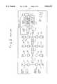
- FIG. 1is a block diagram showing a semiconductor integrated circuit according to a prior art
- FIG. 2is a block diagram showing lines for transmitting a clock signal in the circuit of FIG. 1;
- FIG. 3explains the problem of the circuit of FIG. 2;
- FIG. 4is a block diagram showing a semiconductor integrated circuit according to an embodiment of the present invention.
- FIG. 5is a block diagram showing a semiconductor integrated circuit according to another embodiment of the present invention.
- FIGS. 6A to 6Cshow a delay section of a delay controller according to the present invention
- FIG. 7shows a control section of the delay controller
- FIG. 8is a timing chart showing the operation of the control section of FIG. 7;
- FIG. 9shows a phase comparing section of a phase comparator according to the present invention.
- FIGS. 10A to 10Care timing charts showing the operation of the phase comparing section of FIG. 9;
- FIG. 11shows an amplifying section of the phase comparator
- FIG. 12is a timing chart showing the operation of a JK flip-flop of the amplifying section of FIG. 11;
- FIG. 13is a timing chart showing an incremental operation of the amplifying section of FIG. 11;
- FIG. 14is a timing chart showing a sustain operation of the amplifying section of FIG. 11;
- FIG. 15is a timing chart showing a decremental operation of the amplifying section of FIG. 11;
- FIG. 16shows an SDRAM according to the present invention
- FIG. 17is a timing chart showing the operation of the SDRAM of FIG. 16;
- FIG. 18is a block diagram showing essential parts of the SDRAM of FIG. 16;
- FIG. 19shows a data output buffer of the circuit of FIG. 18
- FIG. 20shows a dummy line for transmitting a dummy internal clock signal in a semiconductor integrated circuit according to the present invention
- FIG. 21shows a memory module according to the present invention.
- FIG. 22shows a memory system according to the present invention.
- FIG. 1is a block diagram showing an example of the DLL circuit according to the prior art.
- the circuithas a clock signal input pad 1, an output circuit 5 serving as an object circuit, a data output pad 6, a phase comparator 3, delay controllers 21 and 22 that control delays in response to the output of the phase comparator 3, a real line 41 for transmitting an internal clock signal from the delay controller 21 to the output circuit 5, and a dummy line 42 having the same load as the real line 41, for transmitting a dummy internal clock signal.
- the phase comparator 3compares the phase of an input signal A, which is a reference signal ⁇ ext and is also supplied to the delay controllers 21 and 22, with the phase of an input signal B, which is a comparison object signal ⁇ out, i.e., the dummy signal. According to the comparison result, the delay controllers 21 and 22 control delays therein so that the signal B is behind the signal A by one clock period. As a result, the internal clock signal supplied to the output circuit 5 is behind the input signal A by one clock period, to apparently suppress a propagation delay in the real line 41.
- Using the dummy line 42 for controlling a delay in the real line 41is advantageous because the dummy and real lines 42 and 41 do not restrict each other's location on a chip. This expands the freedom of designing and wiring the circuit.
- FIG. 2shows lines for transmitting the internal clock signal in the circuit of the prior art of FIG. 1 and explains the problem thereof.
- the circuithas output circuits 50 to 57 and data output pads 60 to 67 (DQ0 TO DQ7) formed on, for example, an SDRAM chip.
- the output circuits 50 to 57serve as output buffers of the SDRAM.
- the output circuits 50 to 57 and output pads 60 to 67are formed at different locations on the chip. Accordingly, the lengths of the real line 41 to the output circuits 50 to 57 are different from one another and involve different loads. If the length DL of the dummy line 42 is adjusted to any one of the lengths of the real line 41, errors will occur in the other lengths.
- the phase of the internal clock signal supplied to the output circuit 53 (54)will synchronize with the phase of the external clock signal supplied to the pad 1.
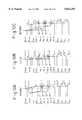
- FIG. 3explains the problem of the prior art of FIG. 2 when applied to an SDRAM.
- tACis a memory access time based on a system clock signal CLK
- tOHis an output data hold time. Due to the property fluctuation, temperature dependency, and source-voltage dependency of the SDRAM, there is a time difference between tAC and tOH.
- the time differenceis a dead band in which data is indefinite and unusable by a memory system.
- the dead bandmay also be extended due to, for example, a wiring delay and a delay fluctuation.
- a systemneeds a setup time tSI and a hold time tHI that must be secured in a period in which the output of the SDRAM is definite. Namely, tSI and tHI must be within a period of tCLK+tOH-tAC.
- output datamust have a predetermined phase with respect to the phase of the external clock signal CLK, i.e., the memory access time tAC must always be constant even if the output circuits 50 to 57 are formed at different locations as shown in FIG. 2. If output data must be synchronized with a rise of the external clock signal CLK, tAC must always be zero.
- Synchronizing an output signal with an external clock signalis important not only for the SDRAM but also for other semiconductor integrated circuits.
- the simplest way to avoid the propagation delay due to the different lengths of the real line 41 to the output circuits 50 to 57is to provide the dummy line 42, phase comparator 3, and delay controllers 21 and 22 for each of the output circuits 50 to 57. This, however, increases a chip area and power consumption. This problem of the prior art commonly occurs in semiconductor integrated circuits such as memory chips, semiconductor integrated circuit modules such as memory modules, and semiconductor integrated circuit systems such as memory systems.
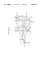
- FIG. 4is a block diagram showing a DLL circuit in a semiconductor integrated circuit according to a first embodiment of the present invention.
- the circuithas an input pad 1 for receiving an external clock signal CLK, a clock signal buffer 10, output circuits 50 to 57 serving as object circuits, data output pads 60 to 67 (DQ0 to DQ7), a first delay controller 21, a second delay controller 22, a phase comparator 3, a real line 41 for transmitting an internal clock signal, and a dummy line 42 for transmitting a dummy internal clock signal.
- the buffer 10In response to the external clock signal CLK supplied through the input pad 1, the buffer 10 provides a signal A ( ⁇ ext) serving as a reference signal to the delay controllers 21 and 22 and phase comparator 3.
- the delay controller 21provides an internal clock signal to the output circuits 50 to 57 through the real line 41.
- the delay controller 22provides a dummy internal clock signal B ( ⁇ out) to the phase comparator 3 through the dummy line 42.
- the phase comparator 3compares the phases of the signals A and B with each other and, according to the comparison result, controls delays in the delay controllers 21 and 22.
- the output circuits 50 to 57 and data output pads 60 to 67are formed at different locations on a chip.
- a node N15is connected to the delay controller 21 through a length RL15 of the real line 41.
- the node N15is so positioned to halve the length RL2 (FIG. 2) of the real line 41 into lengths RL12 and RL13.
- the length DL1 of the dummy line 42is equal to RL15+RL13, or RL15+RL12 of the real line 41.
- a rise or fall of the internal clock signal to the output circuits 52, 55, 51, and 56agrees with a rise or fall of the clock signal A, thereby eliminating an error in the timing of supplying the internal clock signal to the output circuits.
- the output circuits 53, 54, 50, and 57are not provided with a dummy line for the length RL14 or RL11 of the real line 41, they may have a propagation error corresponding to the length. This, however, is smaller than the propagation error on the output circuits 50 and 57 of FIG. 2.
- the first embodimentforms the real line 41 having a symmetrical tree shape between the delay controller 21 and the output circuits 50 to 57, as well as the dummy line 42 with its length DL1 being substantially equal to the length of the real line 41 between the delay controller 21 and a proper one of the nodes connected to the output circuits.
- a delay in the real line 41is canceled with the use of the dummy line 42, so that the location of the DLL circuit in a given semiconductor integrated circuit is unlimited to expand the freedom of designing and wiring the circuit.
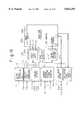
- FIG. 5is a block diagram showing a DLL circuit in a semiconductor integrated circuit according to another embodiment of the present invention.
- First and second delay controllers 21 and 22, a phase comparator 3, etc.,are the same as those of the embodiment of FIG. 4.
- a real line 41has a length RL27 between the delay controller 21 and a node N27, a length RL 25 between the nodes N27 and N25, a length RL26 between the nodes N27 and N26, a length RL21 between the nodes N25 and N21, a length RL22 between the nodes N25 and N22, a length RL23 between the nodes N26 and N23, and a length RL24 between the nodes N26 and N24.
- the node N24must be arranged close to the phase comparator 3 to avoid a delay between them. This results in restricting the layout of the circuit. If the node N24 is adjacent to the phase comparator 3, a delay will occur to break synchronization between the external clock signal CLK and the internal clock signal supplied to the output circuits 50 to 57. To avoid these problems, the present invention employs the second delay controller 22 and dummy line 42.
- FIGS. 6A to 6Cshow a delay section of any one of the delay controllers 21 and 22, in which FIG. 6A shows a 1-bit delay element, FIG. 6B is a time chart showing the operation of the 1-bit delay element, and FIG. 6C shows cascaded 1-bit delay elements.
- the 1-bit delay elementhas two NAND gates 401 and 402 and an inverter 403.
- An enable signal ⁇ Eis high in FIG. 6B to activate the 1-bit delay element.
- the 1-bit delay elementreceives an input signal IN and a signal ⁇ N, which is an output signal of another 1-bit delay element on the right side, and provides an output signal OUT.
- Nodes 4a-1 and 4a-2provide waveforms shown in FIG. 6B.
- the output signal OUTis a signal ⁇ N to another 1-bit delay element on the left side.
- the output signal OUTWhen the signal ⁇ N is low, the output signal OUT is always low. If the signal ⁇ N is high and the signal ⁇ E is low, the output signal OUT is high. If the signal ⁇ N is high with the signal ⁇ E being high and the input signal IN being low, the output signal OUT is high, and with the input signal IN being high, the output signal OUT is low.
- the input signal INrises with the enable signal ⁇ E being high, the input signal IN is transmitted through a path indicated with an arrow mark. If the enable signal ⁇ E is low, the input signal IN is blocked from the path.
- the 1-bit delay elementsare cascaded to form the delay section of the delay controller 21 (22).
- FIG. 6Cshows only three 1-bit delay elements, many elements are cascaded in reality, and each element is provided with a signal line such as ⁇ E-1, ⁇ E-2, or ⁇ E-3 each for transmitting an enable signal ⁇ E. These enable signals are controlled by a control section of the delay controller 21 (22).
- the enable signal ⁇ E-2is high to activate the center 1-bit delay element. If the input signal IN changes from low to high, the NAND gates 401-1 and 401-3 of the left and right 1-bit delay elements block the input signal IN because their enable signals ⁇ E-1 and ⁇ E-3 are each low.
- the NAND gate 401-2 of the center 1-bit delay elementpasses the input signal IN because its enable signal ⁇ E-2 is high.
- the NAND gate 402-2 thereofalso passes the input signal IN because the output signal OUT ( ⁇ N) of the right 1-bit delay element is high. Then, the center 1-bit delay element provides the low output signal OUT. If the output signal OUT ( ⁇ N) of the right 1-bit delay element is low, the output signal OUT of the 1-bit delay element that receives the output signal is always low. Accordingly, the output signal OUT of the center 1-bit delay element is transmitted through the NAND gate and inverter of the left 1-bit delay element and is provided as a final output signal.
- the input signal INis transmitted through an activated 1-bit delay element, to form a final output signal.
- controlling the enable signal ⁇ E of a required 1-bit delay element to highwill control a delay in the delay controller 21 (22).
- the delay of a 1-bit delay elementis determined by the total signal propagation time of the NAND gates and inverter of the element and forms a unit delay time.
- a total delay timeis calculated by multiplying the number of 1-bit delay elements passed by the input signal IN by the unit delay time.
- FIG. 7shows a control section of the delay controller 21 (22) of the present invention.
- the control sectionconsists of 1-bit control elements among which one surrounded with a dotted line in FIG. 7 is a 1-bit control element 430-2. Each element provides an enable signal ⁇ E to a corresponding one of the 1-bit delay elements (FIG. 6).
- the 1-bit control element 430-2consists of a flip-flop having a NAND gate 432-2 and an inverter 433-2, transistors 435-2, 437-2, 438-2, and 439-2, and a NOR gate 431-2.
- the gate of the transistor 438-2is connected to a node 5a-2 of a front 1-bit control element.
- the gate of the transistor 439-2is connected to a node 5a-5 of a rear 1-bit control element.
- Incremental signalsi.e., set signals ⁇ SE and ⁇ SO and decremental signals, i.e., reset signals ⁇ RE and ⁇ RO are connected alternately to the 1-bit control elements.
- the gate of the transistor 435-2receives the set signal ⁇ SO, and the gate of the transistor 437-2 receives the reset signal ⁇ RO.
- the gates of the corresponding transistors of the front and rear 1-bit control elementsreceive the set signal ⁇ SE and reset signal ⁇ RE.
- the NOR gate 431-2receives a signal from a node 5a-1 of the front element and a signal from a node 5a-4 of its own.
- a signal ⁇ Rresets the delay controller 21 (22). The signal ⁇ R is once set to low when a power source is turned on and is fixed to high thereafter.
- FIG. 8is a timing chart showing the operation of the circuit of FIG. 7.
- the reset signal ⁇ Ris once set to low so that the nodes 5a-1, 5a-3, and 5a-5 are set to high and the nodes 5a-2, 5a-4, and 5a-6 to low.
- the incremental signalsi.e., the set signals ⁇ SE and ⁇ SO are set to high and low alternately.
- the enable signal ⁇ E-1changes from high to low. This state is latched by the flip-flop, and therefore, the enable signal ⁇ E-1 keeps the low level even if the set signal ⁇ SE returns to low.
- the enable signal ⁇ E-2changes from low to high.
- the transistor 438-2is turned on.
- the set signal ⁇ SOchanges from low to high
- the node 5a-3is grounded to low
- the node 5a-4changes to high.
- the enable signal ⁇ E-2changes from high to low. This state is latched by the flip-flop, and therefore, the enable signal ⁇ E-2 keeps the low level even if the set signal ⁇ SO returns to low.
- FIG. 8shows each one pulse of the set signals ⁇ SE and ⁇ SO, many 1-bit control elements are connected to one another in reality. Accordingly, if the set signals ⁇ SE and ⁇ SO are alternately set to high and low, the 1-bit control element that provides the enable signal ⁇ E of high level will shift to the right sequentially. If the comparison result from the phase comparator 3 indicates that a delay must be increased, the set signals ⁇ SE and ⁇ SO will alternately be set to high and low.
- the reset signals ⁇ RE and ⁇ ROare alternately provided so that the 1-bit control element that provides the enable signal ⁇ E of high level may shift to the left sequentially.
- control section of FIG. 7 of the delay controller 21 (22)shifts the 1-bit control element that provides an enable signal ⁇ E of high level element by element, to control the 1-bit delay elements of FIG. 6C element by element.
- FIG. 9shows a phase comparing section of the phase comparator 3 according to the present invention
- FIGS. 10A to 10Care timing charts showing the operation of the phase comparing section.
- the phase comparator 3consists of the phase comparing section of FIG. 9 and an amplifying section of FIG. 11.
- the phase comparing sectioncompares the dummy internal clock signal ⁇ out with the external clock signal ⁇ ext serving as a reference signal. Output signals ⁇ a to ⁇ e are transferred to the amplifying section.
- the phase comparing sectionis composed of flip-flops 421 and 422 each having two NAND gates, latches 425 and 426 for latching the states of the flip-flops 421 and 422, respectively, a generator 424 for generating an activation signal for the latches 425 and 426, and a 1-delay circuit 423 for obtaining a phase allowance for the external clock signal ⁇ ext.
- FIG. 10Ashows that the phase of the dummy internal clock signal ⁇ out is ahead of the phase of the reference signal ⁇ ext. Namely, the signal ⁇ out changes from low to high before the signal ⁇ ext shows the same change.
- nodes 6a-2 to 6a-5 of the flip-flops 421 and 422are each high.
- the nodes 6a-2 and 6a-4change from high to low.
- the signal ⁇ extchanges from low to high, and after one unit delay, the node 6a-1 changes from low to high.
- the terminal voltages of the flip-flops 421 and 422are unchanged because they are already fixed. As a result, the node 6a-2 is continuously low, 6a-3 high, 6a-4 low, and 6a-5 high.
- the output signal ⁇ a of the generator 424changes from high to low, to apply a high pulse to the node 6a-6. Since the node 6a-6 is connected to the NAND gates of the latches 425 and 426, the NAND gates are temporarily activated, and the latches 425 and 426 latch the terminal voltages of the flip-flips 421 and 422. As a result, the output signal ⁇ b changes to high, ⁇ c to low, ⁇ d to high, and ⁇ e to low.
- FIG. 10Bshows that the dummy internal clock signal ⁇ out and reference signal ⁇ ext have substantially the same phase and change from low to high substantially at the same time.
- the signal ⁇ outchanges from low to high.
- the signal ⁇ extchanges from low to high, so that the node 6a-3 of the flip-flop 421 changes from high to low.
- the node 6a-1maintains a low level, and the node 6a-4 changes from high to low. Thereafter, the node 6a-1 changes from low to high.
- the state of the flip-flop 422is unchanged.
- the node 6a-6provides a high pulse, and the latches 425 and 426 store the states.
- the output signal ⁇ bchanges to low, ⁇ c to high, ⁇ d to high, and ⁇ e to low.
- FIG. 10Cshows that the phase of the dummy internal clock signal tout is behind the phase of the reference signal ⁇ ext and that the signal ⁇ out changes from low to high after the same change in the signal ⁇ ext.
- the signal ⁇ extcauses changes in the flip-flops 421 and 422, and the nodes 6a-3 and 6a-5 change from high to low.
- the output signal ⁇ bchanges to low, ⁇ c to high, ⁇ d to low, and ⁇ e to high.
- a rise of the reference signal ⁇ extis used to determine whether a rise of the dummy internal clock signal ⁇ out is ahead, simultaneous, or behind.
- the determinationis latched as values of the output signals ⁇ b, ⁇ c, ⁇ d, and ⁇ e. According to these values, it is determined to increment or decrement delays in the delay controllers 21 and 22.
- FIG. 11shows the amplifying section of the phase comparator 3 of the present invention
- FIG. 12is a timing chart showing the operation of a JK flip-flop of the amplifying section.
- the amplifying sectionhas the JK flip-flop 427 and an amplifier 428 consisting of NAND gates and inverters.
- the JK flip-flop 427receives the output signal ⁇ a from the phase comparing section of FIG. 9. In response to the level of the signal ⁇ a, the voltages of nodes 7a-9 and 7a-11 alternate between high and low levels.
- the amplifier 428receives and amplifies the outputs of the JK flip-flip 427 and the signals ⁇ b to ⁇ e.
- the operation of the JK flip-flop 427will be explained with reference to the timing chart of FIG. 12.
- the signal ⁇ achanges from high to low at time T1, and then, nodes 7a-1 and 7a-10 change from low to high.
- Nodes 7a-5, 7a-6, and 7a-7change in response to the change at the node 7a-1, but a node 7a-8 shows no change because the signal ⁇ a is low.
- the output node 7a-9is unchanged, and the output node 7a-11 changes from high to low.
- the signal ⁇ achanges from low to high, and then, the node 7a-8 changes from high to low.
- the node 7a-10is unchanged because the node 7a-7 is unchanged.
- the output node 7a-9changes from low to high, and the output node 7a-11 is unchanged. In this way, the output nodes 7a-9 and 7a-11 of the JK flip-flop 427 alternately change from high to low and from low to high.
- FIG. 13is a timing chart showing an incremental operation of the amplifying section 428 of FIG. 11 of the phase comparator 3
- FIG. 14is a timing chart showing a sustain operation of the same
- FIG. 15is a timing chart showing a decremental operation of the same.
- the dummy internal clock signal ⁇ outchanges from low to high before the same change in the reference signal ⁇ ext.
- the phase comparing section of FIG. 9provides the signal ⁇ b of high, ⁇ c of low, ⁇ d of high, and ⁇ e of low.
- a node 7a-12becomes high, and a node 7a-13 is fixed at low.
- the incremental (set) signals ⁇ SO and ⁇ SEchange in response to the state of the JK flip-flop 427, the decremental (reset) signals ⁇ RO and ⁇ RE are unchanged because the node 7a-13 is low.
- the signal ⁇ outchanges from low to high substantially simultaneously with the reference signal ⁇ ext.
- the phase comparing section of FIG. 9provides the signal ⁇ b of low, ⁇ c of high, ⁇ d of high, and ⁇ e of low.
- the nodes 7a-12 and 71-13are fixed at low.
- the set signals ⁇ SO and ⁇ SEare not influenced by the output of the JK flip-flop, and therefore, the signals ⁇ SO, ⁇ SE, ⁇ RO, and ⁇ RE are fixed at low.
- the signal ⁇ outchanges from low to high behind the same change in the reference signal ⁇ ext.
- the phase comparing section of FIG. 9provides the signal ⁇ b of low, ⁇ c of high, ⁇ d of low, and ⁇ e of high.
- the node 7a-12is fixed at low
- the node 7a-13is fixed at high
- the reset signals ⁇ RO and ⁇ REchange in response to the state of the JK flip-flop
- the set signals ⁇ SO and ⁇ SEare unchanged because the node 7a-12 is low.
- FIG. 16shows an SDRAM employing the DLL circuit of the present invention
- FIG. 17is a timing chart showing the operation of the SDRAM.
- the SDRAMemploys a pipeline method and is a 2-bank, 8-bit, 16-M SDRAM.
- the SDRAMhas DRAM cores 108a and 108b, a clock buffer 101, a command decoder 102, an address buffer/register and bank address selector 103, an I/O data buffer/register 104, control signal latches 105a and 105b, a mode register 106, and column address counters 107a and 107b.
- Signals /CS, /RAS, /CAS, and /WEare combined to form a command that specifies an operation mode.
- the commandis decoded by the command decoder 102, and according to a mode specified by the command, circuits are controlled.
- the signals /CS, /RAS, /CAS, and /WEare also supplied to the latches 105a and 105b that maintain their states until the next command is provided.
- Address signalsare amplified by the address buffer 103, which provides row addresses for the banks as well as initial addresses for the column address counters 107a and 107b.
- the clock buffer 101has an internal clock generator 121 and an output timing controller 122, which is the DLL circuit of the present invention.
- the internal clock generator 121generates an ordinary internal clock signal according to an external clock signal CLK.
- the output timing controller 122generates a delay-locked (phase-locked) clock signal after carrying out the delay control of the present invention mentioned above.
- the register 104has a data input buffer 13 and a data output circuit 5 including output circuits 50 to 57.
- the data output circuit 5amplifies data read out of the DRAM cores 108a and 108b and provides the data through output pads DQ0 to DQ7 according to the delay-locked clock signal provided by the output timing controller 122. Input data to the pads DQ0 to DQ7 are received by the data input buffer 13.
- a real line to which the present invention is appliedruns between the output timing controller 122 and the data output circuit 5.
- FIG. 17shows a read operation of the SDRAM of FIG. 16.
- the external clock signal CLKis supplied from a system to the SDRAM.
- the SDRAMIn synchronization with a rise of the clock signal CLK, the SDRAM reads commands, address signals, and input data and provides output data.
- the command signals /CS, /RAS, /CAS, and /WEare combined to form an active command (ACT), which is supplied to a command terminal.
- ACTactive command
- a row address signalis supplied to an address terminal.
- the SDRAMis activated to select a word line corresponding to the row address, provides corresponding cell data to a corresponding bit line, and amplifies the data by a sense amplifier.
- a read command and a column addressare supplied to the SDRAM.
- the SDRAMselects sense amplifier data according to the column address, supplies the data to a data bus line, amplifies the data by a data bus amplifier, further amplifies the data by the output buffer, and transfers the data to the output terminal DQ.
- These operationsare the same as those of a standard DRAM.
- circuits related to a column addresscarry out a pipeline operation, and read data is continuously provided. Accordingly, a data transfer speed is determined by the period of the external clock signal.
- the SDRAMinvolves three kinds of access time each of which is defined according to a rise of the clock signal CLK.
- FIG. 17there are row address access time tRAC, column address access time tCAC, and clock signal access time tAC.
- tRAC and tCACare important because they determine a period between command input and first data output.
- the clock signal access time tACis also important.
- FIG. 18is a block diagram showing essential parts of the SDRAM of FIG. 16 and explains a pipeline operation thereof with, for example, three pipes.
- the circuit for processing a column address in the SDRAMis divided into several sections along a processing flow. Each of the divided sections is called a pipe.
- the buffer 101has the internal clock generator 121 and output timing controller 122.
- the internal clock generator 121generates an ordinary internal clock signal, which is supplied to the pipes 1 and 2.
- the output timing controller 122provides a delay-locked (phase-locked) internal clock signal to the output circuit 5 (data output circuits 50 to 57) of the pipe 3.
- the supplied internal clock signalscontrol the corresponding pipes. Between the pipes, there is a switch for controlling the transmission timing of a signal between the pipes. These switches are controlled according to the internal clock signal generated by the generator 121.
- a column address buffer 116amplifies an address signal and sends it to a column decoder 118.
- the column decoder 118selects an address.
- Data at the addressis amplified by a sense amplifier 117 and then is supplied to a data bus.
- the data on the data busis amplified by a data bus amplifier 119.
- the pipe 2involves only a data bus controller 120.
- the pipe 3involves the I/O buffer 104 (output circuit 5).
- the data input buffer 13 in the I/O buffer 104is not shown in FIG. 18.
- the circuit(s) in each pipecompletes its operation within a clock cycle, and the switch between the pipes is opened and closed in synchronization with the clock signal, to relay data.
- the pipesprocess data in parallel, and data is continuously sent to the output terminal in synchronization with the clock signal.
- FIG. 19shows an example of the output circuit 5 (output circuits 50 to 57) of FIG. 18.
- Signals Data1 and Data2correspond to data read out of a cell array 115 through the sense amplifier 117, data bus amplifier 119, and data bus controller 120 of FIG. 18.
- the signals Data1 and Data2are each low when the read data is high and are each high when the read data is low. If the read data is not high nor low under a high-impedance (high-Z) state, the data bus controller 120 sets the signal Data1 to high and the signal Data2 to low.
- a signal ⁇ oecorresponds to the internal clock signal from the output timing controller 122 (the first delay controller 21) and serves as an enable signal for the output circuit 5 (output circuits 50 to 57).
- the signals Data1 and Data2appear at the data output pad 6 (output pads 60 to 67).
- the signal ⁇ oechanges from low to high, a node 8a-1 to low, and a node 8a-2 to high, to turn on transfer gates.
- the signals Data1 and Data2are transferred to nodes 8a-3 and 8a-6.
- a node 8a-5changes to low and a node 8a-8 to high, to turn on a p-channel transistor 81 and off an n-channel transistor 82. Consequently, the data output pad 6 provides a signal of high level.
- the transfer gatesare turned off to hold the current output state.
- the present inventionis applicable not only to SDRAMs but also to any semiconductor integrated circuits that provide an output signal in synchronization with an external clock signal.
- FIG. 20shows an example of the dummy line 42 according to the present invention.
- the dummy line 42is formed on a chip and has the same width as the real line 41.
- a dummy line 242 (FIG. 21) formed in a semiconductor integrated circuit module to be explained below and a dummy line 342 (FIG. 22) formed in a semiconductor integrated circuit system to be explained beloware fabricated on a module or on a circuit board. Any dummy line may be replaced with a combination of capacitors or resistors.
- FIG. 21shows a memory module such as a single inline memory module (SIMM) and a dual inline memory module (DIMM) employing the DLL circuit of the present invention.
- the modulehas a clock signal connector 201, memory ICs (object circuits) 250 to 253, a first delay controller 221, a second delay controller 222, a phase comparator 203, a real line 241 for transmitting an internal clock signal, and the dummy line 242 for transmitting a dummy internal clock signal.
- An external clock signal CLKis passed through the clock signal connector 201 and is supplied to the delay controllers 221 and 222 and phase comparator 203.
- the delay controller 221provides the internal clock signal to the memory ICs 250 to 253 through the real line 241, similar to the circuit of FIG. 5.
- the delay controller 222provides the dummy internal clock signal to the phase comparator 203 through the dummy line 242.
- the phase comparator 203compares the phases of the provided two signals, and according to the comparison result, controls delays in the delay controllers 221 and 222.
- the details of the DLL circuitare the same as those explained above.
- the memory ICs 250 to 253correspond to the output circuits 50 to 57 or the output pads 60 to 67 of the circuit of FIG. 5.
- the length DL3 of the dummy line 242is equalized to RL37+RL35+RL31, to synchronize the operation timing of all the memory ICs 250 to 253.
- FIG. 22shows a memory system employing the DLL circuit of the present invention.
- the systemhas a clock signal generator 300, memory modules (object circuits) 350 to 353, a first delay controller 321, a second delay controller 322, a phase comparator 303, a real line 341 for transmitting an internal clock signal, and a dummy line 342 for transmitting a dummy internal clock signal.
- the clock signal generator 300generates a clock signal CLK, which is supplied to the delay controllers 321 and 322 and phase comparator 303.
- the first delay controller 321provides the internal clock signal to the memory modules 350 to 353 through the real line 341, similar to the memory module of FIG. 21.
- the second delay controller 322provides the dummy internal clock signal to the phase comparator 303 through the dummy line 342.
- the phase comparator 303compares the phases of the received two signals, and according to the comparison result, controls delays in the delay controllers 321 and 322. The details of the DLL circuit are as explained above.
- the memory modules 350 to 353correspond to the memory ICs 250 to 253 of the memory module of FIG. 21.
- the length DL4 of the dummy line 342is equalized to RL47+RL45+RL41, to synchronize the operation timing of all the memory modules 350 to 353.
- FIGS. 21 and 22are based on the circuit of FIG. 5, the circuit of FIG. 4 of the present invention is also applicable to memory modules and memory systems.
- the present inventionis applicable not only to memories such as SDRAMs, memory modules, and memory systems but also to other semiconductor integrated circuits, semiconductor integrated circuit modules, and semiconductor integrated circuit systems.
- the present inventionmay control not only a clock signal but also other signals.
- the present inventionprovides a semiconductor integrated circuit that provides a phase-locked control signal to object circuits or pads without regard to the physical locations thereof.
- the present inventionis capable of providing a phase-locked control signal in a semiconductor integrated circuit module and a semiconductor integrated circuit system.
Landscapes
- Engineering & Computer Science (AREA)
- Theoretical Computer Science (AREA)
- Physics & Mathematics (AREA)
- General Engineering & Computer Science (AREA)
- General Physics & Mathematics (AREA)
- Nonlinear Science (AREA)
- Computer Hardware Design (AREA)
- Dram (AREA)
- Semiconductor Integrated Circuits (AREA)
- Design And Manufacture Of Integrated Circuits (AREA)
- Memory System (AREA)
- Stabilization Of Oscillater, Synchronisation, Frequency Synthesizers (AREA)
- Logic Circuits (AREA)
Abstract
Description
Claims (42)
Applications Claiming Priority (2)
| Application Number | Priority Date | Filing Date | Title |
|---|---|---|---|
| JP21388096AJP4070255B2 (en) | 1996-08-13 | 1996-08-13 | Semiconductor integrated circuit |
| JP8-213880 | 1996-08-13 |
Publications (1)
| Publication Number | Publication Date |
|---|---|
| US5822255Atrue US5822255A (en) | 1998-10-13 |
Family
ID=16646552
Family Applications (1)
| Application Number | Title | Priority Date | Filing Date |
|---|---|---|---|
| US08/790,794Expired - LifetimeUS5822255A (en) | 1996-08-13 | 1997-01-30 | Semiconductor integrated circuit for supplying a control signal to a plurality of object circuits |
Country Status (5)
| Country | Link |
|---|---|
| US (1) | US5822255A (en) |
| JP (1) | JP4070255B2 (en) |
| KR (1) | KR100242759B1 (en) |
| GB (1) | GB2316247B (en) |
| TW (1) | TW328998B (en) |
Cited By (67)
| Publication number | Priority date | Publication date | Assignee | Title |
|---|---|---|---|---|
| US5955904A (en)* | 1997-03-21 | 1999-09-21 | Fujitsu Limited | Semiconductor integrated circuit with appropriate data output timing and reduced power consumption |
| US5990730A (en)* | 1998-02-03 | 1999-11-23 | Fujitsu Limited | Semiconductor device with stable operation and reduced power consumption |
| US5995441A (en)* | 1998-04-27 | 1999-11-30 | Mitsubishi Denki Kabushiki Kaisha | Synchronous semiconductor memory device capable of rapidly, highly precisely matching internal clock phase to external clock phase |
| US6066969A (en)* | 1998-01-16 | 2000-05-23 | Fujitsu Limited | Semiconductor device with DLL circuit avoiding excessive power consumption |
| US6078514A (en)* | 1997-09-09 | 2000-06-20 | Fujitsu Limited | Semiconductor device and semiconductor system for high-speed data transfer |
| US6084802A (en)* | 1997-08-11 | 2000-07-04 | Fujitsu Limited | Semiconductor integrated circuit device |
| US6201423B1 (en) | 1996-08-13 | 2001-03-13 | Fujitsu Limited | Semiconductor device, semiconductor system, and digital delay circuit |
| US6476653B1 (en) | 1998-08-14 | 2002-11-05 | Fujitsu Limited | DLL circuit adjustable with external load |
| US6504790B1 (en)* | 2001-08-09 | 2003-01-07 | International Business Machines Corporation | Configurable DDR write-channel phase advance and delay capability |
| US6525585B1 (en)* | 2000-11-21 | 2003-02-25 | Nec Corporation | Fixed-length delay generation circuit |
| US20030101312A1 (en)* | 2001-11-26 | 2003-05-29 | Doan Trung T. | Machine state storage apparatus and method |
| US6608743B1 (en)* | 1999-10-19 | 2003-08-19 | Nec Corporation | Delay locked loop, synchronizing method for the same and semiconductor device equipped with the same |
| US6684278B1 (en)* | 1999-07-16 | 2004-01-27 | Mitsubishi Denki Kabushiki Kaisha | Microcomputer and memory access control method |
| US20040141404A1 (en)* | 1997-10-10 | 2004-07-22 | Rambus Inc. | Power control system for synchronous memory device |
| US20040206683A1 (en)* | 2000-05-04 | 2004-10-21 | Cote Pierre Lucien | Immersed membrane apparatus |
| US6820181B2 (en) | 2002-08-29 | 2004-11-16 | Micron Technology, Inc. | Method and system for controlling memory accesses to memory modules having a memory hub architecture |
| US20050066136A1 (en)* | 2003-09-18 | 2005-03-24 | Schnepper Randy L. | Memory hub with integrated non-volatile memory |
| US20050144403A1 (en)* | 2003-12-29 | 2005-06-30 | Jeddeloh Joseph M. | Memory hub and method for memory system performance monitoring |
| US20050146943A1 (en)* | 2003-08-28 | 2005-07-07 | Jeddeloh Joseph M. | Memory module and method having on-board data search capabilities and processor-based system using such memory modules |
| US20050177677A1 (en)* | 2004-02-05 | 2005-08-11 | Jeddeloh Joseph M. | Arbitration system having a packet memory and method for memory responses in a hub-based memory system |
| US20050198500A1 (en)* | 2004-03-02 | 2005-09-08 | International Business Machines Corporation | System and method for performing security operations on network data |
| US20050198492A1 (en)* | 2004-03-02 | 2005-09-08 | International Business Machines Corporation. | System and method for secure data transfer over a network |
| US6963989B1 (en) | 2000-05-22 | 2005-11-08 | Micron Technology, Inc. | Method and apparatus for adjusting data hold timing of an output circuit |
| US6980042B2 (en) | 2004-04-05 | 2005-12-27 | Micron Technology, Inc. | Delay line synchronizer apparatus and method |
| US7047351B2 (en) | 2002-08-16 | 2006-05-16 | Micron Technology, Inc. | Memory hub bypass circuit and method |
| US20060109146A1 (en)* | 2002-07-09 | 2006-05-25 | Eiichi Takahashi | Digital circuit having a delay circuit for adjustment of clock signal timing |
| US7106611B2 (en) | 2002-09-09 | 2006-09-12 | Micron Technology, Inc. | Wavelength division multiplexed memory module, memory system and method |
| US7107415B2 (en) | 2003-06-20 | 2006-09-12 | Micron Technology, Inc. | Posted write buffers and methods of posting write requests in memory modules |
| US7117316B2 (en) | 2002-08-05 | 2006-10-03 | Micron Technology, Inc. | Memory hub and access method having internal row caching |
| US7120723B2 (en) | 2004-03-25 | 2006-10-10 | Micron Technology, Inc. | System and method for memory hub-based expansion bus |
| US7120727B2 (en) | 2003-06-19 | 2006-10-10 | Micron Technology, Inc. | Reconfigurable memory module and method |
| US7120743B2 (en) | 2003-10-20 | 2006-10-10 | Micron Technology, Inc. | Arbitration system and method for memory responses in a hub-based memory system |
| US7133991B2 (en) | 2003-08-20 | 2006-11-07 | Micron Technology, Inc. | Method and system for capturing and bypassing memory transactions in a hub-based memory system |
| US7133972B2 (en) | 2002-06-07 | 2006-11-07 | Micron Technology, Inc. | Memory hub with internal cache and/or memory access prediction |
| US7136958B2 (en) | 2003-08-28 | 2006-11-14 | Micron Technology, Inc. | Multiple processor system and method including multiple memory hub modules |
| US7139348B1 (en)* | 2002-04-09 | 2006-11-21 | Applied Micro Circuits Corporation | Distributed clock network using all-digital master-slave delay lock loops |
| US7162567B2 (en) | 2004-05-14 | 2007-01-09 | Micron Technology, Inc. | Memory hub and method for memory sequencing |
| US7181584B2 (en) | 2004-02-05 | 2007-02-20 | Micron Technology, Inc. | Dynamic command and/or address mirroring system and method for memory modules |
| US7180522B2 (en) | 2000-06-23 | 2007-02-20 | Micron Technology, Inc. | Apparatus and method for distributed memory control in a graphics processing system |
| US7188219B2 (en) | 2004-01-30 | 2007-03-06 | Micron Technology, Inc. | Buffer control system and method for a memory system having outstanding read and write request buffers |
| US7200024B2 (en) | 2002-08-02 | 2007-04-03 | Micron Technology, Inc. | System and method for optically interconnecting memory devices |
| US7210059B2 (en) | 2003-08-19 | 2007-04-24 | Micron Technology, Inc. | System and method for on-board diagnostics of memory modules |
| US7213082B2 (en) | 2004-03-29 | 2007-05-01 | Micron Technology, Inc. | Memory hub and method for providing memory sequencing hints |
| US7222197B2 (en) | 2003-07-22 | 2007-05-22 | Micron Technology, Inc. | Apparatus and method for direct memory access in a hub-based memory system |
| US7222213B2 (en) | 2004-05-17 | 2007-05-22 | Micron Technology, Inc. | System and method for communicating the synchronization status of memory modules during initialization of the memory modules |
| US7234070B2 (en) | 2003-10-27 | 2007-06-19 | Micron Technology, Inc. | System and method for using a learning sequence to establish communications on a high-speed nonsynchronous interface in the absence of clock forwarding |
| US7242213B2 (en) | 2003-06-11 | 2007-07-10 | Micron Technology, Inc. | Memory module and method having improved signal routing topology |
| US7254331B2 (en) | 2002-08-09 | 2007-08-07 | Micron Technology, Inc. | System and method for multiple bit optical data transmission in memory systems |
| US7257683B2 (en) | 2004-03-24 | 2007-08-14 | Micron Technology, Inc. | Memory arbitration system and method having an arbitration packet protocol |
| US7260685B2 (en) | 2003-06-20 | 2007-08-21 | Micron Technology, Inc. | Memory hub and access method having internal prefetch buffers |
| US7310748B2 (en) | 2004-06-04 | 2007-12-18 | Micron Technology, Inc. | Memory hub tester interface and method for use thereof |
| US7310752B2 (en) | 2003-09-12 | 2007-12-18 | Micron Technology, Inc. | System and method for on-board timing margin testing of memory modules |
| US7330992B2 (en) | 2003-12-29 | 2008-02-12 | Micron Technology, Inc. | System and method for read synchronization of memory modules |
| US7363419B2 (en) | 2004-05-28 | 2008-04-22 | Micron Technology, Inc. | Method and system for terminating write commands in a hub-based memory system |
| US7366864B2 (en) | 2004-03-08 | 2008-04-29 | Micron Technology, Inc. | Memory hub architecture having programmable lane widths |
| US7392331B2 (en) | 2004-08-31 | 2008-06-24 | Micron Technology, Inc. | System and method for transmitting data packets in a computer system having a memory hub architecture |
| US7428644B2 (en) | 2003-06-20 | 2008-09-23 | Micron Technology, Inc. | System and method for selective memory module power management |
| US7447240B2 (en) | 2004-03-29 | 2008-11-04 | Micron Technology, Inc. | Method and system for synchronizing communications links in a hub-based memory system |
| US20080310574A1 (en)* | 2007-06-13 | 2008-12-18 | Hynix Semiconductor Inc. | Semiconductor memory device |
| US7519788B2 (en) | 2004-06-04 | 2009-04-14 | Micron Technology, Inc. | System and method for an asynchronous data buffer having buffer write and read pointers |
| US20090175103A1 (en)* | 1998-04-01 | 2009-07-09 | Mosaid Technologies Incorporated | Semiconductor memory asynchronous pipeline |
| US7590797B2 (en) | 2004-04-08 | 2009-09-15 | Micron Technology, Inc. | System and method for optimizing interconnections of components in a multichip memory module |
| US7788451B2 (en) | 2004-02-05 | 2010-08-31 | Micron Technology, Inc. | Apparatus and method for data bypass for a bi-directional data bus in a hub-based memory sub-system |
| US7805586B2 (en) | 2002-08-29 | 2010-09-28 | Micron Technology, Inc. | System and method for optimizing interconnections of memory devices in a multichip module |
| US8756395B2 (en) | 1998-03-10 | 2014-06-17 | Rambus Inc. | Controlling DRAM at time DRAM ready to receive command when exiting power down |
| CN104916308A (en)* | 2014-03-14 | 2015-09-16 | 爱思开海力士有限公司 | Semiconductor device |
| CN120639088A (en)* | 2025-08-14 | 2025-09-12 | 西北工业大学 | A highly reliable and low-power lock detector |
Families Citing this family (10)
| Publication number | Priority date | Publication date | Assignee | Title |
|---|---|---|---|---|
| CA2805213A1 (en)* | 1998-04-01 | 1999-10-01 | Mosaid Technologies Incorporated | Semiconductor memory asynchronous pipeline |
| US6100733A (en)* | 1998-06-09 | 2000-08-08 | Siemens Aktiengesellschaft | Clock latency compensation circuit for DDR timing |
| JP2002007201A (en)* | 2000-06-21 | 2002-01-11 | Nec Corp | Memory system, memory interface, and memory chip |
| KR100335503B1 (en)* | 2000-06-26 | 2002-05-08 | 윤종용 | Signal transmission circuit, signal transmission method for synchronizing different delay characteristics, and data latch circuit of semiconductor device having the same |
| JP2002015569A (en) | 2000-06-27 | 2002-01-18 | Mitsubishi Electric Corp | Semiconductor device |
| US8327173B2 (en)* | 2007-12-17 | 2012-12-04 | Nvidia Corporation | Integrated circuit device core power down independent of peripheral device operation |
| JP5298527B2 (en)* | 2007-12-24 | 2013-09-25 | 富士通セミコンダクター株式会社 | Variable delay circuit and control method thereof |
| JP2012029211A (en)* | 2010-07-27 | 2012-02-09 | Fujitsu Ltd | Timing adjustment circuit |
| FR3086475B1 (en)* | 2018-09-24 | 2021-05-21 | Moduleus | ELECTRONIC CIRCUIT WITH SYNCHRONIZED CLOCK DISTRIBUTION |
| KR20230134388A (en) | 2022-03-14 | 2023-09-21 | 에스케이하이닉스 주식회사 | Semiconductor devices |
Citations (12)
| Publication number | Priority date | Publication date | Assignee | Title |
|---|---|---|---|---|
| JPH05159080A (en)* | 1991-12-05 | 1993-06-25 | Hitachi Ltd | Logical integrated circuit |
| US5313438A (en)* | 1989-11-20 | 1994-05-17 | Canon Kabushiki Kaisha | Delay apparatus |
| US5313422A (en)* | 1991-05-29 | 1994-05-17 | Texas Instruments Incorporated | Digitally controlled delay applied to address decoder for write vs. read |
| EP0662756A1 (en)* | 1994-01-07 | 1995-07-12 | Oki Electric Industry Co., Ltd. | Clock circuit |
| US5440514A (en)* | 1994-03-08 | 1995-08-08 | Motorola Inc. | Write control for a memory using a delay locked loop |
| US5493538A (en)* | 1994-11-14 | 1996-02-20 | Texas Instruments Incorporated | Minimum pulse width address transition detection circuit |
| US5504715A (en)* | 1993-11-17 | 1996-04-02 | Samsung Electronics Co., Ltd. | Word line loading compensating circuit of semiconductor memory device |
| US5553033A (en)* | 1994-10-07 | 1996-09-03 | Texas Instruments Incorporated | Apparatus and method for an address transition detector summing circuit |
| US5557580A (en)* | 1993-08-18 | 1996-09-17 | Texas Instruments Incorporated | Word line driving circuit |
| US5566130A (en)* | 1995-11-09 | 1996-10-15 | The United States Of America As Represented By The Secretary Of The Air Force | Address transition detection (ATD) circuit for asynchronous VLSI chips |
| US5566108A (en)* | 1994-09-30 | 1996-10-15 | Nec Corporation | Synchronized semiconductor memory |
| US5740123A (en)* | 1996-08-29 | 1998-04-14 | Fujitsu Limited | Semiconductor integrated circuit for changing pulse width according to frequency of external signal |
Family Cites Families (5)
| Publication number | Priority date | Publication date | Assignee | Title |
|---|---|---|---|---|
| US5307381A (en)* | 1991-12-27 | 1994-04-26 | Intel Corporation | Skew-free clock signal distribution network in a microprocessor |
| JPH05233092A (en)* | 1992-02-18 | 1993-09-10 | Nec Ic Microcomput Syst Ltd | Method and circuit for distributing clock signal |
| JPH0722511A (en)* | 1993-07-05 | 1995-01-24 | Mitsubishi Electric Corp | Semiconductor device |
| JP3077866B2 (en)* | 1993-11-18 | 2000-08-21 | 日本電気株式会社 | Memory module |
| JPH08180678A (en)* | 1994-12-27 | 1996-07-12 | Hitachi Ltd | Dynamic RAM |
- 1996
- 1996-08-13JPJP21388096Apatent/JP4070255B2/ennot_activeExpired - Lifetime
- 1997
- 1997-01-30USUS08/790,794patent/US5822255A/ennot_activeExpired - Lifetime
- 1997-01-31GBGB9702083Apatent/GB2316247B/ennot_activeExpired - Fee Related
- 1997-02-03TWTW086101252Apatent/TW328998B/ennot_activeIP Right Cessation
- 1997-02-24KRKR1019970005520Apatent/KR100242759B1/ennot_activeExpired - Lifetime
Patent Citations (12)
| Publication number | Priority date | Publication date | Assignee | Title |
|---|---|---|---|---|
| US5313438A (en)* | 1989-11-20 | 1994-05-17 | Canon Kabushiki Kaisha | Delay apparatus |
| US5313422A (en)* | 1991-05-29 | 1994-05-17 | Texas Instruments Incorporated | Digitally controlled delay applied to address decoder for write vs. read |
| JPH05159080A (en)* | 1991-12-05 | 1993-06-25 | Hitachi Ltd | Logical integrated circuit |
| US5557580A (en)* | 1993-08-18 | 1996-09-17 | Texas Instruments Incorporated | Word line driving circuit |
| US5504715A (en)* | 1993-11-17 | 1996-04-02 | Samsung Electronics Co., Ltd. | Word line loading compensating circuit of semiconductor memory device |
| EP0662756A1 (en)* | 1994-01-07 | 1995-07-12 | Oki Electric Industry Co., Ltd. | Clock circuit |
| US5440514A (en)* | 1994-03-08 | 1995-08-08 | Motorola Inc. | Write control for a memory using a delay locked loop |
| US5566108A (en)* | 1994-09-30 | 1996-10-15 | Nec Corporation | Synchronized semiconductor memory |
| US5553033A (en)* | 1994-10-07 | 1996-09-03 | Texas Instruments Incorporated | Apparatus and method for an address transition detector summing circuit |
| US5493538A (en)* | 1994-11-14 | 1996-02-20 | Texas Instruments Incorporated | Minimum pulse width address transition detection circuit |
| US5566130A (en)* | 1995-11-09 | 1996-10-15 | The United States Of America As Represented By The Secretary Of The Air Force | Address transition detection (ATD) circuit for asynchronous VLSI chips |
| US5740123A (en)* | 1996-08-29 | 1998-04-14 | Fujitsu Limited | Semiconductor integrated circuit for changing pulse width according to frequency of external signal |
Cited By (192)
| Publication number | Priority date | Publication date | Assignee | Title |
|---|---|---|---|---|
| US6201423B1 (en) | 1996-08-13 | 2001-03-13 | Fujitsu Limited | Semiconductor device, semiconductor system, and digital delay circuit |
| US20050242864A1 (en)* | 1996-08-13 | 2005-11-03 | Fujitsu Limited | Semiconductor device, semiconductor system, and digital delay circuit |
| US20030076143A1 (en)* | 1996-08-13 | 2003-04-24 | Fujitsu Limited | Semiconductor device, semiconductor system, and digital delay circuit |
| US6498524B1 (en) | 1996-08-13 | 2002-12-24 | Fujitsu Limited | Input/output data synchronizing device |
| US6298004B1 (en)* | 1996-08-13 | 2001-10-02 | Fujitsu Limited | Semiconductor device, semiconductor system, and digital delay circuit |
| US5955904A (en)* | 1997-03-21 | 1999-09-21 | Fujitsu Limited | Semiconductor integrated circuit with appropriate data output timing and reduced power consumption |
| US6084802A (en)* | 1997-08-11 | 2000-07-04 | Fujitsu Limited | Semiconductor integrated circuit device |
| US6078514A (en)* | 1997-09-09 | 2000-06-20 | Fujitsu Limited | Semiconductor device and semiconductor system for high-speed data transfer |
| US20050180255A1 (en)* | 1997-10-10 | 2005-08-18 | Tsern Ely K. | Memory device having a read pipeline and a delay locked loop |
| US7320082B2 (en) | 1997-10-10 | 2008-01-15 | Rambus Inc. | Power control system for synchronous memory device |
| US20080002516A1 (en)* | 1997-10-10 | 2008-01-03 | Tsern Ely K | Memory Device Having a Delay Locked Loop and Multiple Power Modes |
| US8248884B2 (en) | 1997-10-10 | 2012-08-21 | Rambus Inc. | Method of controlling a memory device having multiple power modes |
| US8305839B2 (en) | 1997-10-10 | 2012-11-06 | Rambus Inc. | Memory device having multiple power modes |
| US7626880B2 (en) | 1997-10-10 | 2009-12-01 | Rambus Inc. | Memory device having a read pipeline and a delay locked loop |
| US7986584B2 (en) | 1997-10-10 | 2011-07-26 | Rambus Inc. | Memory device having multiple power modes |
| US20040141404A1 (en)* | 1997-10-10 | 2004-07-22 | Rambus Inc. | Power control system for synchronous memory device |
| US20100046314A1 (en)* | 1997-10-10 | 2010-02-25 | Tsern Ely K | Memory Device Having a Read Pipeline and a Delay Locked Loop |
| US6066969A (en)* | 1998-01-16 | 2000-05-23 | Fujitsu Limited | Semiconductor device with DLL circuit avoiding excessive power consumption |
| US5990730A (en)* | 1998-02-03 | 1999-11-23 | Fujitsu Limited | Semiconductor device with stable operation and reduced power consumption |
| US8756395B2 (en) | 1998-03-10 | 2014-06-17 | Rambus Inc. | Controlling DRAM at time DRAM ready to receive command when exiting power down |
| US20110202713A1 (en)* | 1998-04-01 | 2011-08-18 | Mosaid Technologies Incorporated | Semiconductor Memory Asynchronous Pipeline |
| US20090175103A1 (en)* | 1998-04-01 | 2009-07-09 | Mosaid Technologies Incorporated | Semiconductor memory asynchronous pipeline |
| US9548088B2 (en) | 1998-04-01 | 2017-01-17 | Conversant Intellectual Property Management Inc. | Semiconductor memory asynchronous pipeline |
| US20100217928A1 (en)* | 1998-04-01 | 2010-08-26 | Ian Mes | Semiconductor Memory Asynchronous Pipeline |
| US7865685B2 (en) | 1998-04-01 | 2011-01-04 | Mosaid Technologies Incorporated | Semiconductor memory asynchronous pipeline |
| US8078821B2 (en) | 1998-04-01 | 2011-12-13 | Mosaid Technologies Incorporated | Semiconductor memory asynchronous pipeline |
| US8122218B2 (en) | 1998-04-01 | 2012-02-21 | Mosaid Technologies Incorporated | Semiconductor memory asynchronous pipeline |
| US8601231B2 (en) | 1998-04-01 | 2013-12-03 | Mosaid Technologies Incorporated | Semiconductor memory asynchronous pipeline |
| US5995441A (en)* | 1998-04-27 | 1999-11-30 | Mitsubishi Denki Kabushiki Kaisha | Synchronous semiconductor memory device capable of rapidly, highly precisely matching internal clock phase to external clock phase |
| US6178123B1 (en) | 1998-04-27 | 2001-01-23 | Mitsubishi Denki Kabushiki Kaisha | Semiconductor device with circuit for phasing internal clock signal |
| US6476653B1 (en) | 1998-08-14 | 2002-11-05 | Fujitsu Limited | DLL circuit adjustable with external load |
| US6684278B1 (en)* | 1999-07-16 | 2004-01-27 | Mitsubishi Denki Kabushiki Kaisha | Microcomputer and memory access control method |
| US6608743B1 (en)* | 1999-10-19 | 2003-08-19 | Nec Corporation | Delay locked loop, synchronizing method for the same and semiconductor device equipped with the same |
| US20040206683A1 (en)* | 2000-05-04 | 2004-10-21 | Cote Pierre Lucien | Immersed membrane apparatus |
| US6963989B1 (en) | 2000-05-22 | 2005-11-08 | Micron Technology, Inc. | Method and apparatus for adjusting data hold timing of an output circuit |
| US7180522B2 (en) | 2000-06-23 | 2007-02-20 | Micron Technology, Inc. | Apparatus and method for distributed memory control in a graphics processing system |
| US6525585B1 (en)* | 2000-11-21 | 2003-02-25 | Nec Corporation | Fixed-length delay generation circuit |
| US6504790B1 (en)* | 2001-08-09 | 2003-01-07 | International Business Machines Corporation | Configurable DDR write-channel phase advance and delay capability |
| US20030101312A1 (en)* | 2001-11-26 | 2003-05-29 | Doan Trung T. | Machine state storage apparatus and method |
| US7139348B1 (en)* | 2002-04-09 | 2006-11-21 | Applied Micro Circuits Corporation | Distributed clock network using all-digital master-slave delay lock loops |
| US8499127B2 (en) | 2002-06-07 | 2013-07-30 | Round Rock Research, Llc | Memory hub with internal cache and/or memory access prediction |
| US7644253B2 (en) | 2002-06-07 | 2010-01-05 | Micron Technology, Inc. | Memory hub with internal cache and/or memory access prediction |
| US20110219196A1 (en)* | 2002-06-07 | 2011-09-08 | Round Rock Research, Llc | Memory hub with internal cache and/or memory access prediction |
| US8195918B2 (en) | 2002-06-07 | 2012-06-05 | Round Rock Research, Llc | Memory hub with internal cache and/or memory access prediction |
| US7945737B2 (en) | 2002-06-07 | 2011-05-17 | Round Rock Research, Llc | Memory hub with internal cache and/or memory access prediction |
| US7133972B2 (en) | 2002-06-07 | 2006-11-07 | Micron Technology, Inc. | Memory hub with internal cache and/or memory access prediction |
| US20060109146A1 (en)* | 2002-07-09 | 2006-05-25 | Eiichi Takahashi | Digital circuit having a delay circuit for adjustment of clock signal timing |
| US7274238B2 (en) | 2002-07-09 | 2007-09-25 | National Institute Of Advanced Industrial Science And Technology | Digital circuit having delay circuit for adjustment of clock signal timing |
| US7382639B2 (en) | 2002-08-02 | 2008-06-03 | Micron Technology, Inc. | System and method for optically interconnecting memory devices |
| US7411807B2 (en) | 2002-08-02 | 2008-08-12 | Micron Technology, Inc. | System and method for optically interconnecting memory devices |
| US7289347B2 (en) | 2002-08-02 | 2007-10-30 | Micron Technology, Inc. | System and method for optically interconnecting memory devices |
| US7200024B2 (en) | 2002-08-02 | 2007-04-03 | Micron Technology, Inc. | System and method for optically interconnecting memory devices |
| US8954687B2 (en) | 2002-08-05 | 2015-02-10 | Micron Technology, Inc. | Memory hub and access method having a sequencer and internal row caching |
| US7117316B2 (en) | 2002-08-05 | 2006-10-03 | Micron Technology, Inc. | Memory hub and access method having internal row caching |
| US7489875B2 (en) | 2002-08-09 | 2009-02-10 | Micron Technology, Inc. | System and method for multiple bit optical data transmission in memory systems |
| US7254331B2 (en) | 2002-08-09 | 2007-08-07 | Micron Technology, Inc. | System and method for multiple bit optical data transmission in memory systems |
| US7047351B2 (en) | 2002-08-16 | 2006-05-16 | Micron Technology, Inc. | Memory hub bypass circuit and method |
| US7415567B2 (en) | 2002-08-16 | 2008-08-19 | Micron Technology, Inc. | Memory hub bypass circuit and method |
| US7149874B2 (en) | 2002-08-16 | 2006-12-12 | Micron Technology, Inc. | Memory hub bypass circuit and method |
| US7249236B2 (en) | 2002-08-29 | 2007-07-24 | Micron Technology, Inc. | Method and system for controlling memory accesses to memory modules having a memory hub architecture |
| US20110167238A1 (en)* | 2002-08-29 | 2011-07-07 | Round Rock Research, Llc | Method and system for controlling memory accesses to memory modules having a memory hub architecture |
| US7908452B2 (en) | 2002-08-29 | 2011-03-15 | Round Rock Research, Llc | Method and system for controlling memory accesses to memory modules having a memory hub architecture |
| US7716444B2 (en) | 2002-08-29 | 2010-05-11 | Round Rock Research, Llc | Method and system for controlling memory accesses to memory modules having a memory hub architecture |
| US8234479B2 (en) | 2002-08-29 | 2012-07-31 | Round Rock Research, Llc | System for controlling memory accesses to memory modules having a memory hub architecture |
| US8086815B2 (en) | 2002-08-29 | 2011-12-27 | Round Rock Research, Llc | System for controlling memory accesses to memory modules having a memory hub architecture |
| US7836252B2 (en) | 2002-08-29 | 2010-11-16 | Micron Technology, Inc. | System and method for optimizing interconnections of memory devices in a multichip module |
| US6820181B2 (en) | 2002-08-29 | 2004-11-16 | Micron Technology, Inc. | Method and system for controlling memory accesses to memory modules having a memory hub architecture |
| US7805586B2 (en) | 2002-08-29 | 2010-09-28 | Micron Technology, Inc. | System and method for optimizing interconnections of memory devices in a multichip module |
| US8190819B2 (en) | 2002-08-29 | 2012-05-29 | Micron Technology, Inc. | System and method for optimizing interconnections of memory devices in a multichip module |
| US7106611B2 (en) | 2002-09-09 | 2006-09-12 | Micron Technology, Inc. | Wavelength division multiplexed memory module, memory system and method |
| US7282947B2 (en) | 2003-06-11 | 2007-10-16 | Micron Technology, Inc. | Memory module and method having improved signal routing topology |
| US7746095B2 (en) | 2003-06-11 | 2010-06-29 | Round Rock Research, Llc | Memory module and method having improved signal routing topology |
| US7557601B2 (en) | 2003-06-11 | 2009-07-07 | Micron Technology, Inc. | Memory module and method having improved signal routing topology |
| US7245145B2 (en)* | 2003-06-11 | 2007-07-17 | Micron Technology, Inc. | Memory module and method having improved signal routing topology |
| US7242213B2 (en) | 2003-06-11 | 2007-07-10 | Micron Technology, Inc. | Memory module and method having improved signal routing topology |
| US8200884B2 (en) | 2003-06-19 | 2012-06-12 | Round Rock Research, Llc | Reconfigurable memory module and method |
| US8732383B2 (en) | 2003-06-19 | 2014-05-20 | Round Rock Research, Llc | Reconfigurable memory module and method |
| US7120727B2 (en) | 2003-06-19 | 2006-10-10 | Micron Technology, Inc. | Reconfigurable memory module and method |
| US7966444B2 (en) | 2003-06-19 | 2011-06-21 | Round Rock Research, Llc | Reconfigurable memory module and method |
| US7818712B2 (en) | 2003-06-19 | 2010-10-19 | Round Rock Research, Llc | Reconfigurable memory module and method |
| US20110029746A1 (en)* | 2003-06-19 | 2011-02-03 | Round Rock Research, Llc | Reconfigurable memory module and method |
| US8127081B2 (en) | 2003-06-20 | 2012-02-28 | Round Rock Research, Llc | Memory hub and access method having internal prefetch buffers |
| US7260685B2 (en) | 2003-06-20 | 2007-08-21 | Micron Technology, Inc. | Memory hub and access method having internal prefetch buffers |
| US7107415B2 (en) | 2003-06-20 | 2006-09-12 | Micron Technology, Inc. | Posted write buffers and methods of posting write requests in memory modules |
| US7529896B2 (en) | 2003-06-20 | 2009-05-05 | Micron Technology, Inc. | Memory modules having a memory hub containing a posted write buffer, a memory device interface and a link interface, and method of posting write requests in memory modules |
| US7437579B2 (en) | 2003-06-20 | 2008-10-14 | Micron Technology, Inc. | System and method for selective memory module power management |
| US7412566B2 (en) | 2003-06-20 | 2008-08-12 | Micron Technology, Inc. | Memory hub and access method having internal prefetch buffers |
| US7428644B2 (en) | 2003-06-20 | 2008-09-23 | Micron Technology, Inc. | System and method for selective memory module power management |
| US7389364B2 (en) | 2003-07-22 | 2008-06-17 | Micron Technology, Inc. | Apparatus and method for direct memory access in a hub-based memory system |
| US8209445B2 (en) | 2003-07-22 | 2012-06-26 | Round Rock Research, Llc | Apparatus and method for direct memory access in a hub-based memory system |
| US7222197B2 (en) | 2003-07-22 | 2007-05-22 | Micron Technology, Inc. | Apparatus and method for direct memory access in a hub-based memory system |
| US7516363B2 (en) | 2003-08-19 | 2009-04-07 | Micron Technology, Inc. | System and method for on-board diagnostics of memory modules |
| US7210059B2 (en) | 2003-08-19 | 2007-04-24 | Micron Technology, Inc. | System and method for on-board diagnostics of memory modules |
| US7913122B2 (en) | 2003-08-19 | 2011-03-22 | Round Rock Research, Llc | System and method for on-board diagnostics of memory modules |
| US7278060B2 (en) | 2003-08-19 | 2007-10-02 | Micron Technology, Inc. | System and method for on-board diagnostics of memory modules |
| US7251714B2 (en) | 2003-08-20 | 2007-07-31 | Micron Technology, Inc. | Method and system for capturing and bypassing memory transactions in a hub-based memory system |
| US7133991B2 (en) | 2003-08-20 | 2006-11-07 | Micron Technology, Inc. | Method and system for capturing and bypassing memory transactions in a hub-based memory system |
| US7136958B2 (en) | 2003-08-28 | 2006-11-14 | Micron Technology, Inc. | Multiple processor system and method including multiple memory hub modules |
| US7873775B2 (en) | 2003-08-28 | 2011-01-18 | Round Rock Research, Llc | Multiple processor system and method including multiple memory hub modules |
| US7386649B2 (en) | 2003-08-28 | 2008-06-10 | Micron Technology, Inc. | Multiple processor system and method including multiple memory hub modules |
| US8244952B2 (en) | 2003-08-28 | 2012-08-14 | Round Rock Research, Llc | Multiple processor system and method including multiple memory hub modules |
| US20110113189A1 (en)* | 2003-08-28 | 2011-05-12 | Round Rock Research, Llc | Multiple processor system and method including multiple memory hub modules |
| US7581055B2 (en) | 2003-08-28 | 2009-08-25 | Micron Technology, Inc. | Multiple processor system and method including multiple memory hub modules |
| US20050146943A1 (en)* | 2003-08-28 | 2005-07-07 | Jeddeloh Joseph M. | Memory module and method having on-board data search capabilities and processor-based system using such memory modules |
| US9082461B2 (en) | 2003-08-28 | 2015-07-14 | Round Rock Research, Llc | Multiple processor system and method including multiple memory hub modules |
| US20100153794A1 (en)* | 2003-09-12 | 2010-06-17 | Round Rock Research, Llc | System and method for on-board timing margin testing of memory modules |
| US7689879B2 (en) | 2003-09-12 | 2010-03-30 | Micron Technology, Inc. | System and method for on-board timing margin testing of memory modules |
| US7958412B2 (en) | 2003-09-12 | 2011-06-07 | Round Rock Research, Llc | System and method for on-board timing margin testing of memory modules |
| US7310752B2 (en) | 2003-09-12 | 2007-12-18 | Micron Technology, Inc. | System and method for on-board timing margin testing of memory modules |
| US7194593B2 (en) | 2003-09-18 | 2007-03-20 | Micron Technology, Inc. | Memory hub with integrated non-volatile memory |
| US8832404B2 (en) | 2003-09-18 | 2014-09-09 | Round Rock Research, Llc | Memory hub with integrated non-volatile memory |
| US20050066136A1 (en)* | 2003-09-18 | 2005-03-24 | Schnepper Randy L. | Memory hub with integrated non-volatile memory |
| US7975122B2 (en) | 2003-09-18 | 2011-07-05 | Round Rock Research, Llc | Memory hub with integrated non-volatile memory |
| US7490211B2 (en) | 2003-09-18 | 2009-02-10 | Micron Technology, Inc. | Memory hub with integrated non-volatile memory |
| US7120743B2 (en) | 2003-10-20 | 2006-10-10 | Micron Technology, Inc. | Arbitration system and method for memory responses in a hub-based memory system |
| US8589643B2 (en) | 2003-10-20 | 2013-11-19 | Round Rock Research, Llc | Arbitration system and method for memory responses in a hub-based memory system |
| US7234070B2 (en) | 2003-10-27 | 2007-06-19 | Micron Technology, Inc. | System and method for using a learning sequence to establish communications on a high-speed nonsynchronous interface in the absence of clock forwarding |
| US7461286B2 (en) | 2003-10-27 | 2008-12-02 | Micron Technology, Inc. | System and method for using a learning sequence to establish communications on a high-speed nonsynchronous interface in the absence of clock forwarding |
| US8392686B2 (en) | 2003-12-29 | 2013-03-05 | Micron Technology, Inc. | System and method for read synchronization of memory modules |
| US7434081B2 (en) | 2003-12-29 | 2008-10-07 | Micron Technology, Inc. | System and method for read synchronization of memory modules |
| US8880833B2 (en) | 2003-12-29 | 2014-11-04 | Micron Technology, Inc. | System and method for read synchronization of memory modules |
| US7360011B2 (en) | 2003-12-29 | 2008-04-15 | Micron Technology, Inc. | Memory hub and method for memory system performance monitoring |
| US20080140904A1 (en)* | 2003-12-29 | 2008-06-12 | Micron Technology, Inc. | Memory hub and method for memory system performance monitoring |
| US7330992B2 (en) | 2003-12-29 | 2008-02-12 | Micron Technology, Inc. | System and method for read synchronization of memory modules |
| US7216196B2 (en) | 2003-12-29 | 2007-05-08 | Micron Technology, Inc. | Memory hub and method for memory system performance monitoring |
| US20070174562A1 (en)* | 2003-12-29 | 2007-07-26 | Micron Technology, Inc. | Memory hub and method for memory system performance monitoring |
| US20050144403A1 (en)* | 2003-12-29 | 2005-06-30 | Jeddeloh Joseph M. | Memory hub and method for memory system performance monitoring |
| US7533213B2 (en) | 2003-12-29 | 2009-05-12 | Micron Technology, Inc. | Memory hub and method for memory system performance monitoring |
| US7188219B2 (en) | 2004-01-30 | 2007-03-06 | Micron Technology, Inc. | Buffer control system and method for a memory system having outstanding read and write request buffers |
| US8788765B2 (en) | 2004-01-30 | 2014-07-22 | Micron Technology, Inc. | Buffer control system and method for a memory system having outstanding read and write request buffers |
| US8504782B2 (en) | 2004-01-30 | 2013-08-06 | Micron Technology, Inc. | Buffer control system and method for a memory system having outstanding read and write request buffers |
| US7181584B2 (en) | 2004-02-05 | 2007-02-20 | Micron Technology, Inc. | Dynamic command and/or address mirroring system and method for memory modules |
| US8694735B2 (en) | 2004-02-05 | 2014-04-08 | Micron Technology, Inc. | Apparatus and method for data bypass for a bi-directional data bus in a hub-based memory sub-system |
| US7412574B2 (en) | 2004-02-05 | 2008-08-12 | Micron Technology, Inc. | System and method for arbitration of memory responses in a hub-based memory system |
| US7788451B2 (en) | 2004-02-05 | 2010-08-31 | Micron Technology, Inc. | Apparatus and method for data bypass for a bi-directional data bus in a hub-based memory sub-system |
| US8291173B2 (en) | 2004-02-05 | 2012-10-16 | Micron Technology, Inc. | Apparatus and method for data bypass for a bi-directional data bus in a hub-based memory sub-system |
| US20050177677A1 (en)* | 2004-02-05 | 2005-08-11 | Jeddeloh Joseph M. | Arbitration system having a packet memory and method for memory responses in a hub-based memory system |
| US9164937B2 (en) | 2004-02-05 | 2015-10-20 | Micron Technology, Inc. | Apparatus and method for data bypass for a bi-directional data bus in a hub-based memory sub-system |
| US7546435B2 (en) | 2004-02-05 | 2009-06-09 | Micron Technology. Inc. | Dynamic command and/or address mirroring system and method for memory modules |
| US20050198500A1 (en)* | 2004-03-02 | 2005-09-08 | International Business Machines Corporation | System and method for performing security operations on network data |
| US8468337B2 (en) | 2004-03-02 | 2013-06-18 | International Business Machines Corporation | Secure data transfer over a network |
| US20050198492A1 (en)* | 2004-03-02 | 2005-09-08 | International Business Machines Corporation. | System and method for secure data transfer over a network |
| US7564976B2 (en) | 2004-03-02 | 2009-07-21 | International Business Machines Corporation | System and method for performing security operations on network data |
| US7596675B2 (en) | 2004-03-08 | 2009-09-29 | Micron Technology, Inc. | Memory hub architecture having programmable lane widths |
| US7366864B2 (en) | 2004-03-08 | 2008-04-29 | Micron Technology, Inc. | Memory hub architecture having programmable lane widths |
| US8015384B2 (en) | 2004-03-08 | 2011-09-06 | Micron Technology, Inc. | Memory hub architecture having programmable lane widths |
| US9274991B2 (en) | 2004-03-08 | 2016-03-01 | Micron Technology, Inc. | Memory hub architecture having programmable lane widths |
| US8775764B2 (en) | 2004-03-08 | 2014-07-08 | Micron Technology, Inc. | Memory hub architecture having programmable lane widths |
| US8555006B2 (en) | 2004-03-24 | 2013-10-08 | Micron Technology, Inc. | Memory arbitration system and method having an arbitration packet protocol |
| US7412571B2 (en) | 2004-03-24 | 2008-08-12 | Micron Technology, Inc. | Memory arbitration system and method having an arbitration packet protocol |
| US7257683B2 (en) | 2004-03-24 | 2007-08-14 | Micron Technology, Inc. | Memory arbitration system and method having an arbitration packet protocol |
| US9032166B2 (en) | 2004-03-24 | 2015-05-12 | Micron Technology, Inc. | Memory arbitration system and method having an arbitration packet protocol |
| US8082404B2 (en) | 2004-03-24 | 2011-12-20 | Micron Technology, Inc. | Memory arbitration system and method having an arbitration packet protocol |
| US7120723B2 (en) | 2004-03-25 | 2006-10-10 | Micron Technology, Inc. | System and method for memory hub-based expansion bus |
| US7174409B2 (en) | 2004-03-25 | 2007-02-06 | Micron Technology, Inc. | System and method for memory hub-based expansion bus |
| US7899969B2 (en) | 2004-03-25 | 2011-03-01 | Round Rock Research, Llc | System and method for memory hub-based expansion bus |
| US7222210B2 (en) | 2004-03-25 | 2007-05-22 | Micron Technology, Inc. | System and method for memory hub-based expansion bus |
| US7610430B2 (en) | 2004-03-25 | 2009-10-27 | Micron Technology, Inc. | System and method for memory hub-based expansion bus |
| US7206887B2 (en) | 2004-03-25 | 2007-04-17 | Micron Technology, Inc. | System and method for memory hub-based expansion bus |
| US8117371B2 (en) | 2004-03-25 | 2012-02-14 | Round Rock Research, Llc | System and method for memory hub-based expansion bus |
| US7370134B2 (en) | 2004-03-25 | 2008-05-06 | Micron Technology, Inc. | System and method for memory hub-based expansion bus |
| US7213082B2 (en) | 2004-03-29 | 2007-05-01 | Micron Technology, Inc. | Memory hub and method for providing memory sequencing hints |
| US7529273B2 (en) | 2004-03-29 | 2009-05-05 | Micron Technology, Inc. | Method and system for synchronizing communications links in a hub-based memory system |
| US7447240B2 (en) | 2004-03-29 | 2008-11-04 | Micron Technology, Inc. | Method and system for synchronizing communications links in a hub-based memory system |
| US7418526B2 (en) | 2004-03-29 | 2008-08-26 | Micron Technology, Inc. | Memory hub and method for providing memory sequencing hints |
| US7605631B2 (en) | 2004-04-05 | 2009-10-20 | Micron Technology, Inc. | Delay line synchronizer apparatus and method |
| US6980042B2 (en) | 2004-04-05 | 2005-12-27 | Micron Technology, Inc. | Delay line synchronizer apparatus and method |
| US8164375B2 (en) | 2004-04-05 | 2012-04-24 | Round Rock Research, Llc | Delay line synchronizer apparatus and method |
| US7590797B2 (en) | 2004-04-08 | 2009-09-15 | Micron Technology, Inc. | System and method for optimizing interconnections of components in a multichip memory module |
| US7870329B2 (en) | 2004-04-08 | 2011-01-11 | Micron Technology, Inc. | System and method for optimizing interconnections of components in a multichip memory module |
| US8438329B2 (en) | 2004-04-08 | 2013-05-07 | Micron Technology, Inc. | System and method for optimizing interconnections of components in a multichip memory module |
| US7162567B2 (en) | 2004-05-14 | 2007-01-09 | Micron Technology, Inc. | Memory hub and method for memory sequencing |
| US7353320B2 (en) | 2004-05-14 | 2008-04-01 | Micron Technology, Inc. | Memory hub and method for memory sequencing |
| US7562178B2 (en) | 2004-05-14 | 2009-07-14 | Micron Technology, Inc. | Memory hub and method for memory sequencing |
| US7266633B2 (en) | 2004-05-17 | 2007-09-04 | Micron Technology, Inc. | System and method for communicating the synchronization status of memory modules during initialization of the memory modules |
| US7222213B2 (en) | 2004-05-17 | 2007-05-22 | Micron Technology, Inc. | System and method for communicating the synchronization status of memory modules during initialization of the memory modules |
| US7363419B2 (en) | 2004-05-28 | 2008-04-22 | Micron Technology, Inc. | Method and system for terminating write commands in a hub-based memory system |
| US7774559B2 (en) | 2004-05-28 | 2010-08-10 | Micron Technology, Inc. | Method and system for terminating write commands in a hub-based memory system |
| US7310748B2 (en) | 2004-06-04 | 2007-12-18 | Micron Technology, Inc. | Memory hub tester interface and method for use thereof |
| US7594088B2 (en) | 2004-06-04 | 2009-09-22 | Micron Technology, Inc. | System and method for an asynchronous data buffer having buffer write and read pointers |
| US7823024B2 (en) | 2004-06-04 | 2010-10-26 | Micron Technology, Inc. | Memory hub tester interface and method for use thereof |
| US7519788B2 (en) | 2004-06-04 | 2009-04-14 | Micron Technology, Inc. | System and method for an asynchronous data buffer having buffer write and read pointers |
| US8239607B2 (en) | 2004-06-04 | 2012-08-07 | Micron Technology, Inc. | System and method for an asynchronous data buffer having buffer write and read pointers |
| US7949803B2 (en) | 2004-08-31 | 2011-05-24 | Micron Technology, Inc. | System and method for transmitting data packets in a computer system having a memory hub architecture |
| US8346998B2 (en) | 2004-08-31 | 2013-01-01 | Micron Technology, Inc. | System and method for transmitting data packets in a computer system having a memory hub architecture |
| US7596641B2 (en) | 2004-08-31 | 2009-09-29 | Micron Technology, Inc. | System and method for transmitting data packets in a computer system having a memory hub architecture |
| US7392331B2 (en) | 2004-08-31 | 2008-06-24 | Micron Technology, Inc. | System and method for transmitting data packets in a computer system having a memory hub architecture |
| US8379784B2 (en)* | 2007-06-13 | 2013-02-19 | Hynix Semiconductor Inc. | Semiconductor memory device |
| US20080310574A1 (en)* | 2007-06-13 | 2008-12-18 | Hynix Semiconductor Inc. | Semiconductor memory device |
| CN104916308A (en)* | 2014-03-14 | 2015-09-16 | 爱思开海力士有限公司 | Semiconductor device |
| CN104916308B (en)* | 2014-03-14 | 2019-02-01 | 爱思开海力士有限公司 | Semiconductor devices |
| CN120639088A (en)* | 2025-08-14 | 2025-09-12 | 西北工业大学 | A highly reliable and low-power lock detector |
Also Published As
| Publication number | Publication date |
|---|---|
| GB2316247A (en) | 1998-02-18 |
| KR19980018035A (en) | 1998-06-05 |
| JP4070255B2 (en) | 2008-04-02 |
| GB2316247B (en) | 2001-01-03 |
| TW328998B (en) | 1998-04-01 |
| GB9702083D0 (en) | 1997-03-19 |
| JPH1055668A (en) | 1998-02-24 |
| KR100242759B1 (en) | 2000-02-01 |
Similar Documents
| Publication | Publication Date | Title |
|---|---|---|
| US5822255A (en) | Semiconductor integrated circuit for supplying a control signal to a plurality of object circuits | |
| US5740123A (en) | Semiconductor integrated circuit for changing pulse width according to frequency of external signal | |
| KR100305546B1 (en) | Semiconductor devices, semiconductor systems and digital delay circuits | |
| JP3769940B2 (en) | Semiconductor device | |
| KR100902795B1 (en) | Interface circuit | |
| US6259288B1 (en) | Semiconductor integrated circuit having a DLL circuit and a special power supply circuit for the DLL circuit | |
| JP3993717B2 (en) | Semiconductor integrated circuit device | |
| KR100321222B1 (en) | Semiconductor device with prompt timing stabilization | |
| US5896347A (en) | Semiconductor memory system using a clock-synchronous semiconductor device and semiconductor memory device for use in the same | |
| US5990715A (en) | Semiconductor integrated circuit using a synchronized control signal | |
| US6738918B2 (en) | High speed data transfer synchronizing system and method | |
| US7855928B2 (en) | System and method for controlling timing of output signals | |
| JP3729582B2 (en) | Semiconductor device, semiconductor device system, and digital delay circuit | |
| CN111418015A (en) | Techniques for command synchronization in memory devices | |
| US6144713A (en) | Delay locked loop circuit for controlling delay time with reduced lock-up time | |
| US11398816B2 (en) | Apparatuses and methods for adjusting a phase mixer circuit | |
| US5926046A (en) | Semiconductor integrated circuit employing smaller number of elements to provide phase-locked clock signal | |
| JPH11273342A (en) | Semiconductor device | |
| Hamamoto et al. | A skew and jitter suppressed DLL architecture for high frequency DDR SDRAMs | |
| JP4159459B2 (en) | Semiconductor device, semiconductor device system, and digital delay circuit | |
| JP4070764B2 (en) | Semiconductor device | |
| JP2004201348A (en) | Semiconductor integrated circuit |
Legal Events
| Date | Code | Title | Description |
|---|---|---|---|
| AS | Assignment | Owner name:FUJITSU LIMITED, JAPAN Free format text:ASSIGNMENT OF ASSIGNORS INTEREST;ASSIGNOR:UCHIDA, TOSHIYA;REEL/FRAME:008418/0506 Effective date:19970117 | |
| STCF | Information on status: patent grant | Free format text:PATENTED CASE | |
| FEPP | Fee payment procedure | Free format text:PAYOR NUMBER ASSIGNED (ORIGINAL EVENT CODE: ASPN); ENTITY STATUS OF PATENT OWNER: LARGE ENTITY | |
| FPAY | Fee payment | Year of fee payment:4 | |
| FPAY | Fee payment | Year of fee payment:8 | |
| AS | Assignment | Owner name:FUJITSU MICROELECTRONICS LIMITED, JAPAN Free format text:ASSIGNMENT OF ASSIGNORS INTEREST;ASSIGNOR:FUJITSU LIMITED;REEL/FRAME:021998/0645 Effective date:20081104 Owner name:FUJITSU MICROELECTRONICS LIMITED,JAPAN Free format text:ASSIGNMENT OF ASSIGNORS INTEREST;ASSIGNOR:FUJITSU LIMITED;REEL/FRAME:021998/0645 Effective date:20081104 | |
| FPAY | Fee payment | Year of fee payment:12 | |
| AS | Assignment | Owner name:FUJITSU SEMICONDUCTOR LIMITED, JAPAN Free format text:CHANGE OF NAME;ASSIGNOR:FUJITSU MICROELECTRONICS LIMITED;REEL/FRAME:024982/0245 Effective date:20100401 | |
| AS | Assignment | Owner name:SOCIONEXT INC., JAPAN Free format text:ASSIGNMENT OF ASSIGNORS INTEREST;ASSIGNOR:FUJITSU SEMICONDUCTOR LIMITED;REEL/FRAME:035508/0637 Effective date:20150302 |