US5818994A - Device for the unadjusted coupling of a number of optical waveguides to a laser array - Google Patents
Device for the unadjusted coupling of a number of optical waveguides to a laser arrayDownload PDFInfo
- Publication number
- US5818994A US5818994AUS08/715,791US71579196AUS5818994AUS 5818994 AUS5818994 AUS 5818994AUS 71579196 AUS71579196 AUS 71579196AUS 5818994 AUS5818994 AUS 5818994A
- Authority
- US
- United States
- Prior art keywords
- grooves
- laser array
- cover
- substrate
- optical waveguides
- Prior art date
- Legal status (The legal status is an assumption and is not a legal conclusion. Google has not performed a legal analysis and makes no representation as to the accuracy of the status listed.)
- Expired - Fee Related
Links
- 230000008878couplingEffects0.000titleclaimsabstractdescription8
- 238000010168coupling processMethods0.000titleclaimsabstractdescription8
- 238000005859coupling reactionMethods0.000titleclaimsabstractdescription8
- 230000003287optical effectEffects0.000titleabstractdescription25
- QNRATNLHPGXHMA-XZHTYLCXSA-N(r)-(6-ethoxyquinolin-4-yl)-[(2s,4s,5r)-5-ethyl-1-azabicyclo[2.2.2]octan-2-yl]methanol;hydrochlorideChemical compoundCl.C([C@H]([C@H](C1)CC)C2)CN1[C@@H]2[C@H](O)C1=CC=NC2=CC=C(OCC)C=C21QNRATNLHPGXHMA-XZHTYLCXSA-N0.000claimsabstractdescription7
- 239000013307optical fiberSubstances0.000claimsabstract3
- 239000000758substrateSubstances0.000claimsdescription9
- 238000005530etchingMethods0.000claimsdescription3
- 229910052710siliconInorganic materials0.000claimsdescription3
- 239000010703siliconSubstances0.000claimsdescription3
- 239000000463materialSubstances0.000description4
- XUIMIQQOPSSXEZ-UHFFFAOYSA-NSiliconChemical compound[Si]XUIMIQQOPSSXEZ-UHFFFAOYSA-N0.000description2
- 239000000835fiberSubstances0.000description2
- 239000011521glassSubstances0.000description2
- 238000000034methodMethods0.000description2
- 238000007792additionMethods0.000description1
- 239000000853adhesiveSubstances0.000description1
- 230000001070adhesive effectEffects0.000description1
- 238000003780insertionMethods0.000description1
- 230000037431insertionEffects0.000description1
- 238000004519manufacturing processMethods0.000description1
Images

Classifications
- G—PHYSICS
- G02—OPTICS
- G02B—OPTICAL ELEMENTS, SYSTEMS OR APPARATUS
- G02B6/00—Light guides; Structural details of arrangements comprising light guides and other optical elements, e.g. couplings
- G02B6/24—Coupling light guides
- G02B6/42—Coupling light guides with opto-electronic elements
- G02B6/4201—Packages, e.g. shape, construction, internal or external details
- G02B6/4249—Packages, e.g. shape, construction, internal or external details comprising arrays of active devices and fibres
- G—PHYSICS
- G02—OPTICS
- G02B—OPTICAL ELEMENTS, SYSTEMS OR APPARATUS
- G02B6/00—Light guides; Structural details of arrangements comprising light guides and other optical elements, e.g. couplings
- G02B6/24—Coupling light guides
- G02B6/42—Coupling light guides with opto-electronic elements
- G02B6/4201—Packages, e.g. shape, construction, internal or external details
- G02B6/4219—Mechanical fixtures for holding or positioning the elements relative to each other in the couplings; Alignment methods for the elements, e.g. measuring or observing methods especially used therefor
- G02B6/4228—Passive alignment, i.e. without a detection of the degree of coupling or the position of the elements
- G02B6/423—Passive alignment, i.e. without a detection of the degree of coupling or the position of the elements using guiding surfaces for the alignment
- G02B6/4231—Passive alignment, i.e. without a detection of the degree of coupling or the position of the elements using guiding surfaces for the alignment with intermediate elements, e.g. rods and balls, between the elements
Definitions
- the inventionconcerns a device for precisely coupling optical waveguides to a laser array.
- each optical waveguideis individually adjusted to the laser array. This is achieved by placing the optical waveguide in the V-shaped groove of a carrier, which precisely defines the horizontal and vertical position of the optical waveguide. The axial position of the optical waveguide in the groove is adjusted by shifting its end in the direction of the laser array. This takes place with the aid of a microscope, which helps to check whether the end of the optical waveguide has reached the intended final position.
- the known methodis very costly, especially if a number of optical waveguides are to be coupled to a laser array.
- the technical problem on which the invention is basedconsists therefore in creating a device that simplifies coupling a number of optical waveguides to a laser array.
- the positioning meanscomprises at least three conical-frustum-shaped depressions formed in the substrate and cover and each containing a ball.
- the ballsmay be made of glass.
- the substrate and coverare made of silicon and the grooves and depressions are formed by anisotropic etching.
- the device according to the inventioneffectively simplifies the coupling of a number of optical waveguides to a laser array. All the prerequisites for precisely coupling the optical waveguides to the laser array have been fulfilled after the device is assembled and the laser array has been attached thereto. It is then only necessary to push the ends of the optical waveguides, which have been ground to a point, to the stop in the rhombic channels and affix them there. Adjustment of the individual optical waveguides is no longer required.
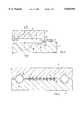
- FIG. 1is a longitudinal section through a configuration example of the device according to the invention.
- FIG. 2is a top view of the device according to FIG. 1, after the cover has been removed;
- FIG. 3is an enlarged section of the device according to FIG. 1, and
- FIG. 4is a cross section of the device along line A-B in FIG. 3.
- FIG. 1illustrates a configuration example of a device, according to the present invention, which comprises a plate 1 and a cover 2.
- a laser array 3is mounted on the plate 1, to which a plurality of optical waveguides or fibers 4 are to be coupled.
- the optical waveguides 4are located in corresponding channels with a rhombic cross section, which is formed by two respective V-shaped grooves in plate 1 and cover 2.
- FIG. 1also shows conical-frustum-shaped depressions 5 in the plate and the cover, with balls 6 arranged therein, which serve to fit the plate 1 and the cover 2 precisely to each other.
- FIG. 2without the cover 2, depicts how the optical waveguides 4 are placed parallel to each other in the V-shaped grooves of the plate 1, which cannot be recognized, and their pointed ends stop at a defined distance from the laser array 3. This distance corresponds to the focal length of the rounded lens-shaped point of the optical waveguide end.
- FIG. 3illustrates how the axial movement of the optical waveguide 4 is limited by stops 9 and 10. This achieves the desired precise distance of the optical waveguide point 4 from the laser array.
- the horizontal and vertical position of the optical waveguide 4is ensured by V-grooves 7 and 8.
- FIG. 4depicts how the V-grooves 7 and 8 form a channel with a rhombic cross section, in which the optical waveguides 4 are arranged in a precise horizontal and vertical position.
- the plate 1 and the cover 2from silicon plates, because in this material the V-grooves 7, 8 and the pyramid-frustum-shaped depressions 5 can be produced with the required accuracy and reproducibility by means of anisotropic etching.
- the balls 6may be made of glass, because balls of this material can be manufactured with a diameter tolerance of ⁇ 1 ⁇ m.
- the devicecan be manufactured in such a way, that the plate 1 and the cover 2 are permanently joined to each other after insertion of the balls. Accordingly, the optical waveguides 4 are pushed to the stops 9 and 10 in the channels formed by the V-grooves 7, 8, and are affixed there by introducing an adhesive material from the end of the device into the gussets of the V-grooves 7, 8 that are not filled by the optical waveguide 4.
Landscapes
- Physics & Mathematics (AREA)
- General Physics & Mathematics (AREA)
- Optics & Photonics (AREA)
- Optical Couplings Of Light Guides (AREA)
- Mechanical Coupling Of Light Guides (AREA)
Abstract
Description
This application is a continuation of application Ser. No. 08/261,842 filed on Jun. 16, 1994 now abandoned.
The invention concerns a device for precisely coupling optical waveguides to a laser array.
In presently used methods for coupling optical waveguides or fibers to a laser array, the end of each optical waveguide is individually adjusted to the laser array. This is achieved by placing the optical waveguide in the V-shaped groove of a carrier, which precisely defines the horizontal and vertical position of the optical waveguide. The axial position of the optical waveguide in the groove is adjusted by shifting its end in the direction of the laser array. This takes place with the aid of a microscope, which helps to check whether the end of the optical waveguide has reached the intended final position.
The known method is very costly, especially if a number of optical waveguides are to be coupled to a laser array.
The technical problem on which the invention is based consists therefore in creating a device that simplifies coupling a number of optical waveguides to a laser array.
This technical problem is solved, according to the present invention, by a flat plate with a number of V-grooves and a flat cover with the same number of V-grooves, which are arranged in the plate and the cover in such a way, that they form rhombic channels after they have been fitted together, wherein the ends of the grooves facing the laser array are equipped with a stop, and the plate and cover are equipped with means for precisely adjusting them in relation to each other.
In further accord with the present invention, the positioning means comprises at least three conical-frustum-shaped depressions formed in the substrate and cover and each containing a ball. The balls may be made of glass.
In still further accord with the present invention, the substrate and cover are made of silicon and the grooves and depressions are formed by anisotropic etching.
The device according to the invention effectively simplifies the coupling of a number of optical waveguides to a laser array. All the prerequisites for precisely coupling the optical waveguides to the laser array have been fulfilled after the device is assembled and the laser array has been attached thereto. It is then only necessary to push the ends of the optical waveguides, which have been ground to a point, to the stop in the rhombic channels and affix them there. Adjustment of the individual optical waveguides is no longer required.
These and other objects, features and advantages of the present invention will become more apparent in light of the following detailed description of a best mode embodiment thereof, as illustrated in the accompanying drawing.
FIG. 1 is a longitudinal section through a configuration example of the device according to the invention;
FIG. 2 is a top view of the device according to FIG. 1, after the cover has been removed;
FIG. 3 is an enlarged section of the device according to FIG. 1, and
FIG. 4 is a cross section of the device along line A-B in FIG. 3.
FIG. 1 illustrates a configuration example of a device, according to the present invention, which comprises aplate 1 and acover 2. Alaser array 3 is mounted on theplate 1, to which a plurality of optical waveguides or fibers 4 are to be coupled. As further elaborated below, the optical waveguides 4 are located in corresponding channels with a rhombic cross section, which is formed by two respective V-shaped grooves inplate 1 andcover 2. FIG. 1 also shows conical-frustum-shaped depressions 5 in the plate and the cover, withballs 6 arranged therein, which serve to fit theplate 1 and thecover 2 precisely to each other.
FIG. 2, without thecover 2, depicts how the optical waveguides 4 are placed parallel to each other in the V-shaped grooves of theplate 1, which cannot be recognized, and their pointed ends stop at a defined distance from thelaser array 3. This distance corresponds to the focal length of the rounded lens-shaped point of the optical waveguide end.
FIG. 3 illustrates how the axial movement of the optical waveguide 4 is limited bystops grooves
FIG. 4 depicts how the V-grooves
In one configuration example, it was proven to be useful to manufacture theplate 1 and thecover 2 from silicon plates, because in this material the V-grooves shaped depressions 5 can be produced with the required accuracy and reproducibility by means of anisotropic etching. However, all other materials with which these results can be achieved, can be used. Theballs 6 may be made of glass, because balls of this material can be manufactured with a diameter tolerance of ±1 μm.
The device can be manufactured in such a way, that theplate 1 and thecover 2 are permanently joined to each other after insertion of the balls. Accordingly, the optical waveguides 4 are pushed to thestops grooves grooves
Although the invention has been shown and described with respect to a best mode embodiment thereof, it should be understood by those skilled in the art that the foregoing and various other changes, omissions and additions in the form and detail thereof may be made therein without departing from the spirit and scope of the invention.
Claims (3)
1. A device for coupling a plurality of optical fibers to a laser array, comprising:
a flat substrate with a plurality of V-grooves and a laser array, ends of the V-grooves adjacent to the laser array being provided with an oblique stop;
a flat cover with a same plurality of V-grooves as said flat substrate, ends of the V-grooves being provided with an oblique stop, said V-grooves of said substrate and cover being arranged to form rhombic channels after said substrate and cover have been fitted together, the ends of the V-grooves of each rhombic channel forming a pointed end stop for placing an optical fiber with a pointed end at a desired precise distance from the laser array after said substrate and cover have been fitted together; and
means for precisely positioning the flat substrate and flat cover relative to each other.
2. A device as claimed in claim 1, wherein said pointed ends are stopped at a selected distance from the laser array, wherein said pointed ends are rounded to form a lens, and wherein said selected distance is a focal length of said lens.
3. A device as claimed in claim 2, wherein the flat substrate and flat cover are made of silicon, and wherein the V-grooves are formed by anisotropic etching.
Priority Applications (1)
| Application Number | Priority Date | Filing Date | Title |
|---|---|---|---|
| US08/715,791US5818994A (en) | 1993-06-18 | 1996-09-19 | Device for the unadjusted coupling of a number of optical waveguides to a laser array |
Applications Claiming Priority (4)
| Application Number | Priority Date | Filing Date | Title |
|---|---|---|---|
| DE4320194.6 | 1993-06-18 | ||
| DE4320194ADE4320194A1 (en) | 1993-06-18 | 1993-06-18 | Device for the adjustment-free coupling of a plurality of optical fibers to a laser array |
| US26184294A | 1994-06-16 | 1994-06-16 | |
| US08/715,791US5818994A (en) | 1993-06-18 | 1996-09-19 | Device for the unadjusted coupling of a number of optical waveguides to a laser array |
Related Parent Applications (1)
| Application Number | Title | Priority Date | Filing Date |
|---|---|---|---|
| US26184294AContinuation | 1993-06-18 | 1994-06-16 |
Publications (1)
| Publication Number | Publication Date |
|---|---|
| US5818994Atrue US5818994A (en) | 1998-10-06 |
Family
ID=6490609
Family Applications (1)
| Application Number | Title | Priority Date | Filing Date |
|---|---|---|---|
| US08/715,791Expired - Fee RelatedUS5818994A (en) | 1993-06-18 | 1996-09-19 | Device for the unadjusted coupling of a number of optical waveguides to a laser array |
Country Status (4)
| Country | Link |
|---|---|
| US (1) | US5818994A (en) |
| EP (1) | EP0629888B1 (en) |
| JP (1) | JPH07140357A (en) |
| DE (2) | DE4320194A1 (en) |
Cited By (13)
| Publication number | Priority date | Publication date | Assignee | Title |
|---|---|---|---|---|
| US6181855B1 (en)* | 1995-12-13 | 2001-01-30 | Deutsche Telekom Ag | Optical and/or electro-optical connection having electromagnetic radiation-produced welds |
| FR2815677A1 (en)* | 2000-10-25 | 2002-04-26 | Commissariat Energie Atomique | Optical component passive alignment method having optical alignment holes upper/lower section placed with balls positioning sections/determining angular offset |
| US20020154866A1 (en)* | 2001-04-02 | 2002-10-24 | Craig Tombling | Alignment of optical fibres with an optical device |
| US6508595B1 (en) | 2000-05-11 | 2003-01-21 | International Business Machines Corporation | Assembly of opto-electronic module with improved heat sink |
| US6628865B2 (en) | 2000-12-15 | 2003-09-30 | Intel Corporation | Alignment of optical fibers to an etched array waveguide |
| US6672773B1 (en) | 2000-12-29 | 2004-01-06 | Amkor Technology, Inc. | Optical fiber having tapered end and optical connector with reciprocal opening |
| US20040037519A1 (en)* | 2002-08-21 | 2004-02-26 | Arnd Kilian | Encapsulated optical fiber end-coupled device |
| US6707970B2 (en) | 2000-12-15 | 2004-03-16 | Intel Corporation | Alignment of fiber optic bundle to array waveguide using an epoxy |
| US6712527B1 (en) | 2000-01-12 | 2004-03-30 | International Business Machines Corporation | Fiber optic connections and method for using same |
| US20040170359A1 (en)* | 2003-03-01 | 2004-09-02 | Benne Velsher | Method for attaching multiple light sources to an optoelectronic module |
| US6865324B1 (en)* | 2001-07-11 | 2005-03-08 | Shipley Company, L.L.C. | Fiber array with passive alignment |
| US6886989B2 (en)* | 2000-12-15 | 2005-05-03 | Intel Corporation | Alignment of fiber optic bundle to array waveguide using pins |
| US20080107417A1 (en)* | 2006-09-27 | 2008-05-08 | Xyratex Technology Limited | Optical wavelength division multiplexed multiplexer/demultiplexer for an optical printed circuit board and a method of manufacturing the same |
Families Citing this family (2)
| Publication number | Priority date | Publication date | Assignee | Title |
|---|---|---|---|---|
| GB2335504B (en)* | 1998-05-28 | 2000-01-26 | Bookham Technology Ltd | Assembly of optical component and optical fibre |
| DE10233203B4 (en)* | 2002-07-22 | 2006-08-03 | Mergeoptics Gmbh | Module with a light guide and method of manufacture |
Citations (12)
| Publication number | Priority date | Publication date | Assignee | Title |
|---|---|---|---|---|
| US4802727A (en)* | 1985-10-16 | 1989-02-07 | British Telecommunications Public Limited Company | Positioning optical components and waveguides |
| US4812002A (en)* | 1986-10-24 | 1989-03-14 | Hitachi, Ltd. | Optical coupling device and method of making the same |
| EP0331334A2 (en)* | 1988-03-03 | 1989-09-06 | AT&T Corp. | Optical connector |
| US5046809A (en)* | 1989-09-29 | 1991-09-10 | Siemens Aktiengesellschaft | Coupling arrangement for optically coupling a fiber to a planar optical waveguide integrated on a substrate |
| EP0466134A2 (en)* | 1990-07-11 | 1992-01-15 | Gte Laboratories Incorporated | Method and device for passive alignment of diode lasers and optical fibers |
| US5121457A (en)* | 1991-05-21 | 1992-06-09 | Gte Laboratories Incorporated | Method for coupling laser array to optical fiber array |
| US5179609A (en)* | 1991-08-30 | 1993-01-12 | At&T Bell Laboratories | Optical assembly including fiber attachment |
| US5182782A (en)* | 1990-07-11 | 1993-01-26 | Gte Laboratories Incorporated | Waferboard structure and method of fabricating |
| US5243673A (en)* | 1989-08-02 | 1993-09-07 | E. I. Du Pont De Nemours And Company | Opto-electronic component having positioned optical fiber associated therewith |
| US5259054A (en)* | 1992-01-10 | 1993-11-02 | At&T Bell Laboratories | Self-aligned optical subassembly |
| US5351331A (en)* | 1993-09-17 | 1994-09-27 | Motorola, Inc. | Method and apparatus for splicing optical fibers with signal I/O |
| US5412748A (en)* | 1992-12-04 | 1995-05-02 | Kabushiki Kaisha Toshiba | Optical semiconductor module |
- 1993
- 1993-06-18DEDE4320194Apatent/DE4320194A1/ennot_activeWithdrawn
- 1994
- 1994-06-17DEDE59409492Tpatent/DE59409492D1/ennot_activeExpired - Fee Related
- 1994-06-17JPJP6135874Apatent/JPH07140357A/enactivePending
- 1994-06-17EPEP94109391Apatent/EP0629888B1/ennot_activeExpired - Lifetime
- 1996
- 1996-09-19USUS08/715,791patent/US5818994A/ennot_activeExpired - Fee Related
Patent Citations (13)
| Publication number | Priority date | Publication date | Assignee | Title |
|---|---|---|---|---|
| US4802727A (en)* | 1985-10-16 | 1989-02-07 | British Telecommunications Public Limited Company | Positioning optical components and waveguides |
| US4812002A (en)* | 1986-10-24 | 1989-03-14 | Hitachi, Ltd. | Optical coupling device and method of making the same |
| EP0331334A2 (en)* | 1988-03-03 | 1989-09-06 | AT&T Corp. | Optical connector |
| US5243673A (en)* | 1989-08-02 | 1993-09-07 | E. I. Du Pont De Nemours And Company | Opto-electronic component having positioned optical fiber associated therewith |
| US5046809A (en)* | 1989-09-29 | 1991-09-10 | Siemens Aktiengesellschaft | Coupling arrangement for optically coupling a fiber to a planar optical waveguide integrated on a substrate |
| US5182782A (en)* | 1990-07-11 | 1993-01-26 | Gte Laboratories Incorporated | Waferboard structure and method of fabricating |
| EP0466134A2 (en)* | 1990-07-11 | 1992-01-15 | Gte Laboratories Incorporated | Method and device for passive alignment of diode lasers and optical fibers |
| US5121457A (en)* | 1991-05-21 | 1992-06-09 | Gte Laboratories Incorporated | Method for coupling laser array to optical fiber array |
| US5179609A (en)* | 1991-08-30 | 1993-01-12 | At&T Bell Laboratories | Optical assembly including fiber attachment |
| EP0529947A1 (en)* | 1991-08-30 | 1993-03-03 | AT&T Corp. | Optical assembly including fiber attachment |
| US5259054A (en)* | 1992-01-10 | 1993-11-02 | At&T Bell Laboratories | Self-aligned optical subassembly |
| US5412748A (en)* | 1992-12-04 | 1995-05-02 | Kabushiki Kaisha Toshiba | Optical semiconductor module |
| US5351331A (en)* | 1993-09-17 | 1994-09-27 | Motorola, Inc. | Method and apparatus for splicing optical fibers with signal I/O |
Cited By (25)
| Publication number | Priority date | Publication date | Assignee | Title |
|---|---|---|---|---|
| US6282346B1 (en) | 1995-12-13 | 2001-08-28 | Deutsche Telekom Ag | Process for producing optical and/or electro-optical connection |
| US6181855B1 (en)* | 1995-12-13 | 2001-01-30 | Deutsche Telekom Ag | Optical and/or electro-optical connection having electromagnetic radiation-produced welds |
| US6712527B1 (en) | 2000-01-12 | 2004-03-30 | International Business Machines Corporation | Fiber optic connections and method for using same |
| DE10065034B4 (en)* | 2000-01-12 | 2006-01-19 | International Business Machines Corp. | Fiber optic port and method of using the same |
| US6508595B1 (en) | 2000-05-11 | 2003-01-21 | International Business Machines Corporation | Assembly of opto-electronic module with improved heat sink |
| US6822875B2 (en) | 2000-05-11 | 2004-11-23 | International Business Machines Corporation | Assembly of opto-electronic module with improved heat sink |
| FR2815677A1 (en)* | 2000-10-25 | 2002-04-26 | Commissariat Energie Atomique | Optical component passive alignment method having optical alignment holes upper/lower section placed with balls positioning sections/determining angular offset |
| WO2002035138A1 (en)* | 2000-10-25 | 2002-05-02 | Commissariat A L"Energie Atomique | Method for passive alignment of supports, particularly plates bearing optical components |
| US20050213896A1 (en)* | 2000-10-25 | 2005-09-29 | Francois Marion | Process and device for the passive alignment of supports, particularly plates comprising optical components |
| US20050180716A1 (en)* | 2000-12-15 | 2005-08-18 | Crafts Douglas E. | Alignment of fiber optic bundle to array waveguide using pins |
| US6707970B2 (en) | 2000-12-15 | 2004-03-16 | Intel Corporation | Alignment of fiber optic bundle to array waveguide using an epoxy |
| US6628865B2 (en) | 2000-12-15 | 2003-09-30 | Intel Corporation | Alignment of optical fibers to an etched array waveguide |
| US6886989B2 (en)* | 2000-12-15 | 2005-05-03 | Intel Corporation | Alignment of fiber optic bundle to array waveguide using pins |
| US6672773B1 (en) | 2000-12-29 | 2004-01-06 | Amkor Technology, Inc. | Optical fiber having tapered end and optical connector with reciprocal opening |
| US6728450B2 (en) | 2001-04-02 | 2004-04-27 | Kamelian Limited, A Body Corporate | Alignment of optical fibers with an optical device |
| US20020154866A1 (en)* | 2001-04-02 | 2002-10-24 | Craig Tombling | Alignment of optical fibres with an optical device |
| US6865324B1 (en)* | 2001-07-11 | 2005-03-08 | Shipley Company, L.L.C. | Fiber array with passive alignment |
| US20040037519A1 (en)* | 2002-08-21 | 2004-02-26 | Arnd Kilian | Encapsulated optical fiber end-coupled device |
| US6786654B2 (en) | 2002-08-21 | 2004-09-07 | Hymite A/S | Encapsulated optical fiber end-coupled device |
| US6807346B2 (en) | 2003-03-01 | 2004-10-19 | Optovia Corporation | Method for attaching multiple light sources to an optoelectronic module |
| US20040170359A1 (en)* | 2003-03-01 | 2004-09-02 | Benne Velsher | Method for attaching multiple light sources to an optoelectronic module |
| US20080107417A1 (en)* | 2006-09-27 | 2008-05-08 | Xyratex Technology Limited | Optical wavelength division multiplexed multiplexer/demultiplexer for an optical printed circuit board and a method of manufacturing the same |
| US7805033B2 (en)* | 2006-09-27 | 2010-09-28 | Xyratex Technology Limited | Optical wavelength division multiplexed multiplexer/demultiplexer for an optical printed circuit board and a method of manufacturing the same |
| US20100290737A1 (en)* | 2006-09-27 | 2010-11-18 | Xyratex Technology Limited | Optical wavelength division multiplexed multiplexer/demultiplexer for an optical printed circuit board and a method of manufacturing the same |
| US8007965B2 (en) | 2006-09-27 | 2011-08-30 | Xyratex Technology Limited | Optical wavelength division multiplexed multiplexer/demultiplexer for an optical printed circuit board and a method of manufacturing the same |
Also Published As
| Publication number | Publication date |
|---|---|
| EP0629888A3 (en) | 1995-01-18 |
| JPH07140357A (en) | 1995-06-02 |
| DE4320194A1 (en) | 1994-12-22 |
| DE59409492D1 (en) | 2000-09-28 |
| EP0629888A2 (en) | 1994-12-21 |
| EP0629888B1 (en) | 2000-08-23 |
Similar Documents
| Publication | Publication Date | Title |
|---|---|---|
| US5818994A (en) | Device for the unadjusted coupling of a number of optical waveguides to a laser array | |
| US5185846A (en) | Optical fiber alignment apparatus including guiding and securing plates | |
| US5135590A (en) | Optical fiber alignment method | |
| US6928226B2 (en) | Fiber and lens grippers, optical devices and methods of manufacture | |
| US4767174A (en) | Process and device for connecting an optical fibre and an integrated optical component comprising a wave guide | |
| US4930854A (en) | Optical fiber-to-channel waveguide coupler | |
| US4057448A (en) | Optical fiber splicing technique | |
| US5432876A (en) | Illumination devices and optical fibres for use therein | |
| US5009475A (en) | Image transfer device and method of manufacture | |
| US6810195B2 (en) | Securing optical elements and optical devices | |
| EP0032722A1 (en) | Optical fiber connectors | |
| US6766076B2 (en) | Optical module and method for assembling the same | |
| US20080008419A1 (en) | Fibre-Lens Arrangement and Lens Array for One Such Fibre-Lens Arrangement | |
| WO1987005119A1 (en) | Array connector for optical fibers | |
| US4636030A (en) | Optical alignment apparatus utilizing prismatic elements | |
| JPH02244012A (en) | Optical device for light collimation | |
| US20040165822A1 (en) | Optical module and production method therefor | |
| EP0382511A3 (en) | Array splice for ribbon-like multi-core optical fibers | |
| DE69737474T2 (en) | METHOD AND SYSTEM FOR COUPLING A WAVE-LEADER TO A COMPONENT | |
| US20020131703A1 (en) | Fiber-lens coupling system and method of manufactuing thereof | |
| CA1090179A (en) | Positioning substrate for optical fibres | |
| US5071217A (en) | Precision focusing and locating collar for a fiber optic connector | |
| DE4313493A1 (en) | Arrangement for coupling an optical waveguide to a light-emitting or receiving element | |
| JPH11305151A (en) | Coupling part of optical switch and method of manufacturing the same | |
| US6636671B2 (en) | Markings for aligning fiber optic bundle |
Legal Events
| Date | Code | Title | Description |
|---|---|---|---|
| FEPP | Fee payment procedure | Free format text:PAYOR NUMBER ASSIGNED (ORIGINAL EVENT CODE: ASPN); ENTITY STATUS OF PATENT OWNER: LARGE ENTITY | |
| FPAY | Fee payment | Year of fee payment:4 | |
| AS | Assignment | Owner name:AVANEX CORPORATION, CALIFORNIA Free format text:ASSIGNMENT OF ASSIGNORS INTEREST;ASSIGNOR:ALCATEL;REEL/FRAME:014083/0012 Effective date:20030731 | |
| LAPS | Lapse for failure to pay maintenance fees | ||
| STCH | Information on status: patent discontinuation | Free format text:PATENT EXPIRED DUE TO NONPAYMENT OF MAINTENANCE FEES UNDER 37 CFR 1.362 | |
| FP | Lapsed due to failure to pay maintenance fee | Effective date:20061006 |