US5818757A - Analog and multi-level memory with reduced program disturb - Google Patents
Analog and multi-level memory with reduced program disturbDownload PDFInfo
- Publication number
- US5818757A US5818757AUS08/684,788US68478896AUS5818757AUS 5818757 AUS5818757 AUS 5818757AUS 68478896 AUS68478896 AUS 68478896AUS 5818757 AUS5818757 AUS 5818757A
- Authority
- US
- United States
- Prior art keywords
- voltage
- word
- line
- memory
- row
- Prior art date
- Legal status (The legal status is an assumption and is not a legal conclusion. Google has not performed a legal analysis and makes no representation as to the accuracy of the status listed.)
- Expired - Lifetime
Links
- 230000015654memoryEffects0.000titleclaimsabstractdescription199
- 238000000034methodMethods0.000claimsdescription14
- 230000005684electric fieldEffects0.000description9
- 230000005641tunnelingEffects0.000description7
- 239000004065semiconductorSubstances0.000description6
- 238000003491arrayMethods0.000description4
- 230000008878couplingEffects0.000description4
- 238000010168coupling processMethods0.000description4
- 238000005859coupling reactionMethods0.000description4
- 238000002347injectionMethods0.000description4
- 239000007924injectionSubstances0.000description4
- 238000010586diagramMethods0.000description3
- 238000009825accumulationMethods0.000description2
- 239000002784hot electronSubstances0.000description2
- 230000005236sound signalEffects0.000description2
- 230000001960triggered effectEffects0.000description2
- 230000005689Fowler Nordheim tunnelingEffects0.000description1
- 230000006978adaptationEffects0.000description1
- 230000000295complement effectEffects0.000description1
- 230000003247decreasing effectEffects0.000description1
Images


Classifications
- G—PHYSICS
- G11—INFORMATION STORAGE
- G11C—STATIC STORES
- G11C16/00—Erasable programmable read-only memories
- G11C16/02—Erasable programmable read-only memories electrically programmable
- G11C16/06—Auxiliary circuits, e.g. for writing into memory
- G11C16/34—Determination of programming status, e.g. threshold voltage, overprogramming or underprogramming, retention
- G11C16/3418—Disturbance prevention or evaluation; Refreshing of disturbed memory data
- G11C16/3427—Circuits or methods to prevent or reduce disturbance of the state of a memory cell when neighbouring cells are read or written
- G—PHYSICS
- G11—INFORMATION STORAGE
- G11C—STATIC STORES
- G11C11/00—Digital stores characterised by the use of particular electric or magnetic storage elements; Storage elements therefor
- G11C11/56—Digital stores characterised by the use of particular electric or magnetic storage elements; Storage elements therefor using storage elements with more than two stable states represented by steps, e.g. of voltage, current, phase, frequency
- G11C11/5621—Digital stores characterised by the use of particular electric or magnetic storage elements; Storage elements therefor using storage elements with more than two stable states represented by steps, e.g. of voltage, current, phase, frequency using charge storage in a floating gate
- G11C11/5628—Programming or writing circuits; Data input circuits
- G11C11/5635—Erasing circuits
- G—PHYSICS
- G11—INFORMATION STORAGE
- G11C—STATIC STORES
- G11C16/00—Erasable programmable read-only memories
- G11C16/02—Erasable programmable read-only memories electrically programmable
- G11C16/06—Auxiliary circuits, e.g. for writing into memory
- G11C16/08—Address circuits; Decoders; Word-line control circuits
- G—PHYSICS
- G11—INFORMATION STORAGE
- G11C—STATIC STORES
- G11C16/00—Erasable programmable read-only memories
- G11C16/02—Erasable programmable read-only memories electrically programmable
- G11C16/06—Auxiliary circuits, e.g. for writing into memory
- G11C16/10—Programming or data input circuits
- G—PHYSICS
- G11—INFORMATION STORAGE
- G11C—STATIC STORES
- G11C27/00—Electric analogue stores, e.g. for storing instantaneous values
- G11C27/005—Electric analogue stores, e.g. for storing instantaneous values with non-volatile charge storage, e.g. on floating gate or MNOS
- G—PHYSICS
- G11—INFORMATION STORAGE
- G11C—STATIC STORES
- G11C16/00—Erasable programmable read-only memories
- G11C16/02—Erasable programmable read-only memories electrically programmable
- G11C16/06—Auxiliary circuits, e.g. for writing into memory
- G11C16/34—Determination of programming status, e.g. threshold voltage, overprogramming or underprogramming, retention
- G11C16/3418—Disturbance prevention or evaluation; Refreshing of disturbed memory data
- G—PHYSICS
- G11—INFORMATION STORAGE
- G11C—STATIC STORES
- G11C7/00—Arrangements for writing information into, or reading information out from, a digital store
- G11C7/16—Storage of analogue signals in digital stores using an arrangement comprising analogue/digital [A/D] converters, digital memories and digital/analogue [D/A] converters
- G—PHYSICS
- G11—INFORMATION STORAGE
- G11C—STATIC STORES
- G11C8/00—Arrangements for selecting an address in a digital store
- G11C8/14—Word line organisation; Word line lay-out
Definitions
- This inventionrelates to non-volatile semiconductor memory and particularly to methods and circuits for reducing disturbance of the stored analog or multi-level data when writing other data.
- Non-volatile semiconductor memoriessuch as EPROM, EEPROM, and Flash memories are well known.
- a threshold voltage of a memory cellindicates a data value stored in the memory cell.
- programming voltagesare applied via a word-line connected to a control gate of the selected cell, a bit-line connected to a drain of the selected cell, and a source-line coupled to a source of the selected cell.
- the combination of programming voltageschanges the threshold voltage of the selected cell typically by causing Fowler-Nordheim (F-N) tunnelling or channel hot electron (CHE) injection which charges (or discharges) a floating gate in the selected memory cell.
- F-NFowler-Nordheim
- CHEchannel hot electron
- the word-line voltage for the selected cellis about 12 volts or higher; and the bit-line voltage for the selected cell is typically about 6 volts higher than the source-line voltage (ground) for the selected cell.
- the high bit-line and word-line voltages for the selected memory cellcan create large voltage differences between the float gate and drain or control gate of unselected memory cells and thereby induce Fowler-Nordheim tunneling that disturbs threshold voltages of unselected memory cells.
- the voltage difference between the drain and floating gate of an unselected memory cellsubjects the memory cell to a disturb referred to herein as drain disturb.
- the voltage difference between the control gate and the floating gate of an unselected memory cellsubjects the memory cell to a disturb referred to herein as gate disturb.
- drain disturbis more severe than gate disturb because the magnitude of the electric field in a tunnel layer between the floating gate and the drain is greater than the electric field in an interpoly dielectric layer between the floating gate and the control gate and because the tunneling current I which disturbs a threshold voltage depends exponentially on an electric field E as indicated in equation 1.
- the disturbance of threshold voltagescan accumulate through repeated programming of memory cells in the same column or row and change the data values stored in unselected cells.
- a data value stored in a memory cellmay be binary (a bit 0 or 1), multi-level (a value from a set of discrete values), or analog (a value within a continuous range of possible values).
- the accumulated disturbance of a threshold voltagemust be relatively large (on the order of a volt or more) to change the threshold voltage from a state indicating a first binary value to a state indicating the second binary value.
- distinguishable threshold voltage differences for data valuescan be a few millivolts, and any small disturbances of threshold voltages limit the theoretically achievable threshold voltage resolution. Accordingly, methods and circuits which reduce disturbance of threshold voltages in multi-level and analog non-volatile memories are sought.
- One way to reduce threshold voltage disturbis to reduce bit-line and word-line lengths by arranging memory cells in several small arrays rather than one large array. With small arrays, fewer memory cells are on the same row or column so that programming a selected memory cell disturbs fewer unselected memory cells; and the accumulated programming disturb time for each memory cell is less. For example, dividing a large array into four small arrays can divide bit-line and word-line lengths in half and reduce accumulation of threshold voltage disturbance in half. However, four small arrays have about twice the overhead in decoding circuitry as does one large array containing the same number of memory cells. Methods and circuits which reduce disturbance of threshold voltages and have low overhead costs are still needed.
- applying a bias voltage to control gates of unselected memory cells containing data valuesreduces drain disturb.
- the bias voltageincreases the voltage of the floating gate (making the floating gate voltage less negative) through capacitive coupling between the control gate and the floating gate and thus reduces the voltage difference between the floating gate and the drain in memory cells in the same column as a selected memory cell being programmed.
- the bias voltageis too low to cause a gate disturb in other memory cells but still significantly reduces drain disturb because the F-N tunneling current which causes the drain disturb depends exponentially on an electric field which the bias voltage reduces.
- the bias voltageis only applied to word-lines of rows which currently hold data values, and the bias voltage is selected to be less than the minimum threshold voltage of memory cells storing data. This avoids turning on any of the unselected memory cells and avoids increasing current drawn during programming. Erased memory cells may have threshold voltages below the bias voltage, but the bias voltage is not applied to the unselected memory cells which are in the erased state so that those memory cells also remain off during programming. Application of a bias voltage to erased memory cells is not required because a small disturbance of the threshold voltage of an erased cell does not affect data values or operation of the memory.
- One embodiment of the inventionis a memory where data values are written sequentially to fill one row of memory cells with data before beginning to write to the next row.
- Memories according to this embodimentare particularly suited for storing a sequence of values representing analog or multi-level samples of a continuous signal such as an audio signal.
- the bias voltageis applied to the word-lines associated with the filled rows.
- a latch, register, flip-flop, or other memory device inside row decoding circuitrycan be set to indicate which rows are filled and therefore selected to have the bias voltage applied.
- FIG. 1shows a prior art non-volatile semiconductor memory.
- FIG. 2illustrates a portion of a non-volatile semiconductor memory in accordance with an embodiment of the invention.
- FIG. 3shows a circuit diagram of row decoding circuitry in accordance with an embodiment of the invention.
- FIG. 4shows timing diagrams for the embodiment of the invention shown in FIG. 3.
- FIG. 5shows a row decoding circuit for a non-volatile memory in accordance with another embodiment of the invention.
- An erasable non-volatile semiconductor memory arraysuch as an EPROM, EEPROM, of Flash memory conventionally includes memory cells organized into rows and columns where each memory cell includes a floating gate transistor or another device which has a threshold voltage that can be set to indicate stored data values.
- FIG. 1illustrates a conventional erasable non-volatile memory 100 and memory array 150 which includes M rows and N columns of memory cells C11 to CMN.
- each memory cell C11 to CMNis a single floating gate transistor which has a control gate coupled to one of word-lines WL1 to WLM, a drain coupled to one of bit-lines BL1 to BLN, and a source connected to a common source-line SL.
- programming voltagesare applied to the word-line and bit-line coupled to the selected memory cell and to the common source-line SL.
- source-line SLis grounded; and a row decoder 130 and a column decoder 110 apply programming voltages to word-line WL1 and bit-line BL1.
- the magnitudes of the programming voltagesdepend on structure of memory cells C11 to CMN and may depend on the data value being written.
- memory array 150is a typical Flash memory array, programming voltages of about 12 volts on word-line WL1, about 6 volts on bit-line BL1, and 0 volts (ground or Vss) on source-line SL, respectively program memory cell C11 by channel hot electron (CHE) injection.
- row decoder 130contains word-line drivers WLD1 to WLDM which apply a programming voltage Vpp to the word-line selected by a decoder tree 140 during a write.
- the word-line drivers WLD1 to WLDMconventionally ground unselected word-lines.
- Column decoder 110applies the programming voltage to the selected bit line and disconnects unselected bit-lines BL2 to BLN.
- a tunneling current I through an insulating layersuch as an interpoly or tunnel dielectric layer in a non-volatile memory cell theoretically depends exponentially on an electric field E in the insulating layer.
- a and Bare constants, typically about 2.5 ⁇ 10 -6 amp/V 2 and 2.5 ⁇ 10 8 V/cm respectively.
- the electric field E1 or E2 in the interpoly or tunnel dielectricdepends on a voltage drop V1 or V2 across an effective oxide thickness Tipox of the interpoly dielectric or an effective oxide thickness Ttox of the tunnel layer.
- Voltage Vfgis the voltage on the floating gate of the memory cell. Equation 3 indicates the dependence of the floating gate voltage Vfg on: the change ⁇ V in threshold voltage from an erased state to a programmed state; the gate, source, and drain voltages Vg, Vs, and Vd of the memory cell; and the floating gate's capacitive couplings Cg, Cs, and Cd to the control gate, the source, and the drain respectively.
- Ctis the total capacitance (Cd+Cs+Cg).
- coupling ratios Cg/Ct, Cd/Ct, and Cs/Ctare 0.65, 0.1, and 0.25 respectively.
- Table 1shows exemplary voltages in memory cells C11, C21, C12, and C22 when writing to memory cell C22.
- voltages Vg, Vs, Vd, ⁇ V, Vfg, V1, and V2are given in volts.
- Voltage V2is the voltage across the tunnel layer between the drain and the floating gate
- voltage V1is the voltage across the interpoly dielectric between the control gate and the floating gate.
- the electric field E2 in the tunnel layer of memory cell C12is more than about twice the electric field E1 in the interpoly dielectric of memory cell C21 because the tunnel layer is typically less than half the thickness of the interpoly dielectric.
- the worst case for drain disturboccurs when memory cell C12 which is in the same column as the selected memory cell has a high threshold voltage.
- the drain disturb for memory cell C21 which is in the selected rowis largest when the threshold voltage of memory cell C21 is low, but the worst case drain disturb of memory cell C21 is still much less than the worst case for memory cell C12. Accordingly, the tunneling current which causes drain disturb in memory cell C12 (and in the other memory cells C32 to CM2 in the selected column) is the primary concern when reducing stress or disturbance of stored data values.
- drain disturbis reduced by applying a bias voltage Vbias to word-lines corresponding to unselected memory cells to which data was written.
- Vbiasbias voltage
- the capacitive coupling between the control gate and the floating gate of these unselected cellsincreases the potential of the floating gate in proportion to the bias voltage and thereby reduces the voltage drop across the tunnel layer between the drain and floating gate of memory cells subject to drain disturb.
- a bias voltage Vbias of about 1.5 voltslowers voltage drop V2 across the tunnel layer by about 1 volt for a typical Flash memory cell experiencing drain disturb. This reduces the tunneling current by about two orders of magnitude for the worst case cell C12.
- Cells such as memory cell C11 which are not in the same row or column as selected memory cell C22also have their control gate voltage Vg raised, but disturb caused by the increase in control gate voltage Vg is insignificant (orders of magnitude less than the drain disturb of cells in the selected column).
- the drain disturb of memory cells such as memory cell C12 which are in the selected columndrops to a level about equal to the drain disturb of memory cells such as memory cell C21 which are in the selected row. Accordingly, for the example of Table 2, drain disturb in selected row becomes the limiting disturbance.
- the reduction in the tunneling current causing a drain disturbresults in a substantial reduction in threshold voltage disturbance per write.
- the reduction in the tunneling currentproportionally increases the maximum number of memory cells on a bit line (i.e. the number of word-lines and the size of an array) allowed when a limit on accumulated threshold voltage disturb must be maintained.
- Memory cell density in analog and multi-level memorycan therefore be increased providing more storage without extensive overhead in integrated circuit area.
- bias voltage Vbiasis only applied to a memory cell if voltage Vbias is less than the threshold voltage of the memory cell. A lower voltage (or ground potential) is applied to the unselected memory cells having threshold voltage below bias voltage Vbias.
- One embodiment of the inventionis a Flash memory for storing analog data.
- Flash memoryafter an erase of a memory array in the Flash memory, memory cells in the array have a distribution of threshold voltages; but the threshold voltages are all less than a cut-off voltage marking a boundary of an erased state for the memory cells.
- Writing an analog data value to a memory cellraises the threshold voltage of the memory cell to a level within a range that is in one-to-one correspondence with the possible analog data values storable in the memory cell.
- the range of programmed threshold voltageshas a lower boundary which is above the cut-off voltage for the erased state so that all erased memory cells are written to by increasing their threshold voltages.
- the memory cells in the arrayhave threshold voltages between about 0.5 volts and about 1.5 volts.
- the minimum threshold voltage corresponding to a data valuecan be selected to be 2.0 volts or higher so that the selected bias voltage Vbias is below the minimum threshold voltage corresponding to a data value. Accordingly, applying the bias voltage does not turn on any memory cells that store data.
- bias voltage Vbiascan be above the threshold voltages of some or all memory cells in the erased state because unselected word-lines connected to memory cells in the erased state are grounded during programming rather than being at bias voltage Vbias. Reducing disturbance of erased memory cells is not critical because such disturbances do not change any data values.
- FIG. 2illustrates part of a non-volatile semiconductor memory 200 in accordance with an embodiment of the invention.
- Memory 200includes an array 150 of memory cells C11 to CMN as described above.
- Memory cells C11 to CMNare single transistor floating gate memory cells, but other embodiments of the invention may employ other types of memory cells.
- an address signal generator 120During programming of a selected memory cell, an address signal generator 120 generates a row address signal and a column address signal which identify the selected memory cell, and a column decoder 110 and a row decoder 230 generate programming voltages on a selected bit-line and a selected word-line corresponding to the selected memory cell.
- Row decoder 230includes a decoder tree 240, bias flag circuits F1 to FM, and word-line drivers D1 to DM.
- Bias flag circuits F1 to FMindicate which rows contain stored data and which rows do not. After each erase of memory array 150, all of bias flag circuits F1 to FM indicate none of rows contain data values.
- decoder tree 240asserts the one of select signals SELECT1 to SELECTM which corresponds to the selected row, and the one of drivers D1 to DM to which the select signal is asserted applies a programming voltage to the selected word-line.
- each bias flag circuit F1 to FMacts as a volatile memory cell or latch which is set when the associated word-line WL1 to WLM is selected during a write. Flag circuits F1 to FM can be cleared when array 150 is erased or alternatively before each memory operation including reading from and writing to memory array 150.
- drivers D1 to DMIn addition to programming voltage on the selected word-line, drivers D1 to DM also apply bias voltage Vbias to some unselected word-lines and ground other unselected word-lines. Whether particular ones of word-lines WL1 to WLM are grounded or at bias voltage Vbias when unselected depends on signal BIAS -- SELECT1 to BIAS -- SELECTM from the associated bias flag circuits F1 to FM. If a bias flag circuit indicates that an unselected row contains stored data, the associated word-line driver applies bias voltage Vbias to the unselected word-line. If the flag circuit indicates that an unselected row contains no data, the associated word-line grounds the unselected word-line.
- memory 200stores a series of samples representing a continuous signal such as an audio signal.
- Each sampleis an analog value or a multi-level value which is written into one of memory cells C11 to CMN.
- address signal generator 120selects where each sample is written and generates consecutive address signals so that a row of memory cells is filled with data values before writing samples to the next row begins. For example, samples can be written sequentially beginning with memory cell C11 which is in the first row and first column.
- a row address signal generator 224asserts a row address which causes decoder tree 240 to assert signal SELECT1 and set bias flag circuit F1 to indicate row C11 . . . C1N contains data.
- Programming voltagesare applied to the first (i.e. selected) word-line WL1; and while a data value is written to memory cell C11, all of the unselected word-lines WL2 to WLM are grounded because all of bias flag circuits F2 to FM were cleared following an erase.
- the row address signalremains constant and the same select signal SELECT1 remains asserted while a column address signal generator 222 sequentially increments the column address signal for writing data values in row C11 . . . C1N.
- the gate programming voltageis applied to first word-line WL1 while writing to the first row.
- row address signal generator 224increments the row address signal, and writing continues with memory cells in the second row C21 . . . C2N.
- word-line driver D2asserts the programming voltage to the selected second word-line WL2.
- Unselected word-lines WL3 to WLMare grounded when programming memory cells in row C21 . . .
- driver D1 for the now unselected first row C11 . . . C1Napplies bias voltage Vbias to word-line WL1 because associated bias flag circuit F1 asserts a signal indicating the first row contains data. None of the memory cells in the first row conduct because each memory cell has been programmed to a threshold voltage level above bias voltage Vbias.
- two unselected word-lines WL1 and WL2are at bias voltage Vbias during programming. Programming continues in this fashion until the last row CM1 . . . CMN is programmed.
- bias flag circuits F1 to FMcan be level triggered latches or edge triggered registers which are set when an associated word-line is selected. Bias flag circuits F1 to FM can alternatively be replaced with a shift register that shifts each time the row address signal changes. Alternatively, a non-volatile memory cell from each row in array 150 can be programmed to indicate whether the remainder of memory cells in a row are in an erased state. In yet another embodiment of the invention, bias flag circuits F1 to FM do not have memory capabilities but instead use the row address signal to directly determine whether rows 1 to M contain data. Rows having row addresses lower than a row selected for a write contain data if memory cells are sequentially programmed.
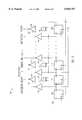
- FIG. 3shows row decoding circuitry 300 for programming a row of a non-volatile analog or multi-level memory cells connected to word-line WL2 of memory 200 (FIG. 2).
- Decoding circuitry 300includes a decoder tree 340, a bias flag circuit F2, and a word-line driver D2 which are associated with word-line WL2.
- Decoding circuitry 300 for word-line WL2is an example of similar decoding circuitry for each of word-lines WL1 to WLM.
- Bias flag circuit F2contains a p-channel transistor 331 and a n-channel transistors 333 which are connected in series between ground and a supply voltage Vcc. Similar p-channel transistor 332 and n-channel transistor 334 are connected in series between voltage Vcc and ground. The gates of transistors 331 and 333 are connected to a node 338 between transistors 332 and 334, and the gates of transistors 332 and 334 are connected to a node 337 between transistors 331 and 333. In the manner of a standard SRAM cell, the voltages at nodes 337 and 338 are complementary and indicate a binary value stored in bias flag circuit F2.
- Bias flag circuit F2also contains a transistor 336 which is connected in parallel with transistor 333. At the beginning of any operation such as writing or reading or after an erase, a signal RESET is asserted high to the gate of transistor 336 to ground node 337 and reset bias flag circuit F2 to a state where signal BIAS -- SELECT2 is high, indicating word-line WL2 is not selected for application of bias voltage Vbias during programming. Similar circuits in decoding circuits for the other rows of the array are similarly reset by signal RESET. Once all bias flag circuits are reset, memory cells in the array can be selected and programmed if the memory cells were previously erased.
- FIG. 4shows a pulse beginning at time 410 before a write operation.
- a similar reset pulseis generated before a read operation.
- Resetting bias flag circuits F1 to FM before a read operationallows decoder tree 340 to select a row for a read but prevents the bias voltage from being applied to unselected word-lines WL1 to WLM during the read.
- the maximum drain voltagecan be kept less than 1.5 volts making the drain disturb orders of magnitude smaller than the programming disturb so that biasing unselected word-lines above the ground potential is not required.
- a transistor 339 between voltage Vcc and transistors 331 and 335disconnects voltage Vcc from transistors 335 and 331 during a read. Accordingly, during a read, node 337 cannot be raised nor signal BIAS -- SELECT2 asserted.
- transistor 339applies voltage Vcc to transistors 335 and 331.
- Decoder tree 340generates a signal SELECT2 which indicates whether word-line WL2 is the selected word-line.
- a signal PRECHARGE and transistors 341 and 344control dynamic precharge for select signal SELECT2.
- a signal PRECHARGEis asserted low which turns on a p-channel transistor 341, turns off an n-channel transistor 344, and charges a node 342 providing signal SELECT2 to a voltage Vcp.
- a charge pump or other high voltage source(not shown) supplies voltage Vcp which is greater than or equal to programming voltage Vpp.
- Row address signals AO to AX and AO to AXare applied to decoder tree 340 during precharge which charges a conducting string of transistors 343 connected to node 342.
- Signal DISCHARGEis simultaneously asserted high which causes a transistor 329 to discharge any voltage remaining on word-line WL2.
- signal PRECHARGEgoes high, signal SELECT2 remains high unless transistors 343 all conduct and pull signal SELECT2 low.
- a unique combination of row address signals AO to AX and their complements AO to AXis connected to the gates of transistors 343 in each copy of decode circuitry 300 so that only one row is selected.
- Signals SELECT2 and BIAS -- SELECT2control driver D2 and determine the voltage applied to word-line WL2 during a write. Between times 430 and 440, data values are written to the first row, word-line WL2 is unselected, and all of the memory cells connected to word-line WL2 are in the erased state. Accordingly, signals SELECT2 and BIAS -- SELECT2 are both high. Signal being high shuts off p-channel transistors 322 and 324 in driver D2 and disables application of a programming voltage Vpp and a verify voltage Vvfy to word-line WL2. Signal SELECT2 being high also turns on n-channel transistors 326 and 327.
- Signal BIAS -- SELECT2being high turns on an n-channel transistor 328 and turns off a p-channel transistor 325. Accordingly, word-line WL2 is grounded through transistors 327 and 328, and is not connected to bias voltage Vbias through transistors 325 and 326.
- signals PRECHARGE and DISCHARGEare again asserted in preparation for changing the row address signal to select word-line WL2.
- Signal SELECT2is applied to the gate of a p-channel transistor 335 which is connected in parallel with transistor 331. Transistor 335 is off which leaves signal BIAS -- SELECT2 unchanged while signal SELECT2 is high.
- signal PRECHARGEis deasserted high
- decoder tree 340pulls signal SELECT2 low, and transistor 335 pulls node 337 high causing signal BIAS -- SELECT2 to fall.
- Signal BIAS -- SELECT2remains low.
- Signal BIAS -- SELECT2 being lowshuts off transistor 328 and disconnects word-line WL2 from ground.
- Signal SELECT2 being lowturns on p-channel transistors 322 and 324 which connects word-line WL2 to p-channel transistors 321 and 323 and enables application of voltages Vpp and Vvfy.
- N-channel transistor 326is turned off disabling application of bias voltage Vbias.
- FIG. 4shows the voltage applied to word-line WL2 after time 450 when word-line WL2 is first selected for programming.
- the programming process illustrated in FIG. 4uses a series of programming pulses 452 which are separated by a series of verify cycles 454.
- a signal PGMis asserted low which turns on a p-channel transistor 321 and drives word-line WL2 to programming voltage Vpp (typically about 12 volts).
- Programming voltage Vppcombined with a programming voltage (typically about 6 volts) applied to the bit-line of the selected memory cell and a grounding of a source-line cause CHE injection which increases the threshold voltage of the selected cell.
- VFYis asserted low while signal PGM is high. This turns on a p-channel transistor 323 and shuts off p-channel transistor 321 so that word-line WL2 is driven to voltage Vvfy. Voltage Vvfy at a level indicating the data value being written and is therefore within the range of threshold voltages indicating data values (typically between 2 volts and 5 volts).
- a sense circuitdetermines whether the selected memory cell conducts while voltage Vvfy is applied to the control gate of the selected memory cell. The voltage on the selected bit-line during a verify cycle is decreased to about 1.5 volts.
- the threshold voltage of the selected memory cellis about equal to voltage Vvfy and is at the desired threshold voltage to represent the analog or multi-level data value being written. Further programming pulses 452 are terminated, and the write to the selected memory cell is complete.
- the row address signalremains constant while each cell in a selected row is programmed in the same manner described above.
- voltage Vvfychanges according to the data value being written.
- Voltage Vppcan be constant or can vary according to the data value being written.
- signal PRECHARGEis asserted low again, and the row address signal is changed to select the next row (i.e. word-line WL3).
- signal SELECT2goes high, signal BIAS -- SELECT2 remains low.
- Signal SELECT2being high disables application of the programming voltage to word-line WL2 and turns on transistor 326.
- Vbiasvoltage Vbias is targeted to be about 1.5 volts which is less than the minimum threshold voltage of memory cells storing data values.
- row address signal generator 224, decoder tree 240, and bias-flag circuits F1 to FM in memory 200can be replaced by a row decoder 500 shown in FIG. 5.
- Row decoder 500includes a set of flip-flops FF0 to FFM coupled in a series with a data output terminal Q of each preceding flip-flop FFI coupled to a data input D of a following flip-flop FF(I+1). The data input terminal of flip-flop FF0 is coupled to supply voltage Vcc.
- Flip-flops FF0 to FFMare all reset before each operation such as a write or a read of memory array 150.
- XOR gates X1 to XMhave input terminals coupled to data output terminals of two consecutive flip-flops and generate signals which high voltage inverters 525 convert to signals SELECT1 to SELECTM. Initially, all data output signals from flip-flops FF0 to FFM are low, and inverters 525 set row select signals SELECT1 to SELECTM to voltage Vcp to indicate no rows are selected.
- a first pulse of a signal CLOCKcauses the output of flip-flop FF0 to go high, the output signal from XOR gate X1 to go high, and signal SELECT1 to go low selecting the first row.
- Clock signal CLOCKnext clocks flip-flops FF0 to FFM when writing or reading of the first row is complete.
- the data output signals from flip-flops FF0 and FF1are high causing output signal from XOR gate Xi to fall and signal SELECT1 to go high.
- the output from XOR gate X2goes high, and signal SELECT2 falls to select the second row for reading or writing.
- Signal CLOCKclocks flip-flops FF0 to FFM in this same fashion after each row of memory array 150 is written or read, and each time flip-flops FF0 to FFM are clocked the next one of signals SELECT1 to SELECTM selects a corresponding row in array 150. Accordingly, the rows of array 150 are sequentially selected.
- Inverters 530generate signals BIAS -- SELECT1 to BIAS -- SELECTM from the data output signals of flip-flops FF0 to FF(M-1). Initially, all of the data output signals of flip-flops FF0 to FFM are low causing all of signals BIAS -- SELECT1 to BIAS -- SELECTM to be high. Each time signal CLOCK clocks flip-flops FF0 to FFM another of the data output signals goes high and unselected rows are sequentially selected for application of word-line bias voltage Vbias. Inverters 530 are disabled during a read so that none of the unselected rows have a bias voltage applied during a read.
Landscapes
- Engineering & Computer Science (AREA)
- Computer Hardware Design (AREA)
- Read Only Memory (AREA)
Abstract
Description
I=A.sup.* E.sup.2 * e.sup.-B/E
I=A.sup.* E.sup.2* e.sup.-B/E
E1=V1/Tipox=(Vg-Vfg)/Tipox
E2=V2/Ttox=(Vd-Vfg)/Ttox
Vfg= Cd.sup.* Vd+Cs.sup.* Vs+Cg.sup.* Vg-Cg.sup.* δV!/Ct
TABLE 1 ______________________________________ Cell Vg Vs Vd δV Vfg V1 V2 E1 E2 ______________________________________ C22 12 0 6 1 4 C21 12 0 0 1 7.2 4.9 -7.2 2.4 -7.2 4 5.2 6.8 -5.2 3.4 -5.2 C12 0 0 6 1 -.05 .05 6.1 .03 6.1 4 -2 2.0 8.0 1.0 8.0 C11 0 0 0 1 -0.7 0.7 0.7 0.3 0.7 4 -2.6 2.6 2.6 1.3 2.6 ______________________________________
TABLE 2 ______________________________________ Cell Vg Vs Vd δV Vfg V1 V2 E1 E2 ______________________________________ C22 12 0 6 1 4 C21 12 0 0 1 7.2 4.9 -7.2 2.4 -7.2 4 5.2 6.8 -5.2 3.4 -5.2 C12 1.5 0 6 1 0.9 0.6 5.1 0.3 5.1 4 -1 2.5 7.0 1.3 7.0 C11 1.5 0 0 1 0.3 1.2 -0.3 0.6 -0.3 4 -1.6 3.1 1.6 1.6 1.6 ______________________________________
Claims (24)
Priority Applications (1)
| Application Number | Priority Date | Filing Date | Title |
|---|---|---|---|
| US08/684,788US5818757A (en) | 1996-07-22 | 1996-07-22 | Analog and multi-level memory with reduced program disturb |
Applications Claiming Priority (1)
| Application Number | Priority Date | Filing Date | Title |
|---|---|---|---|
| US08/684,788US5818757A (en) | 1996-07-22 | 1996-07-22 | Analog and multi-level memory with reduced program disturb |
Publications (1)
| Publication Number | Publication Date |
|---|---|
| US5818757Atrue US5818757A (en) | 1998-10-06 |
Family
ID=24749572
Family Applications (1)
| Application Number | Title | Priority Date | Filing Date |
|---|---|---|---|
| US08/684,788Expired - LifetimeUS5818757A (en) | 1996-07-22 | 1996-07-22 | Analog and multi-level memory with reduced program disturb |
Country Status (1)
| Country | Link |
|---|---|
| US (1) | US5818757A (en) |
Cited By (49)
| Publication number | Priority date | Publication date | Assignee | Title |
|---|---|---|---|---|
| US5910915A (en)* | 1992-01-14 | 1999-06-08 | Sandisk Corporation | EEPROM with split gate source side injection |
| US6002152A (en)* | 1992-01-14 | 1999-12-14 | Sandisk Corporation | EEPROM with split gate source side injection with sidewall spacers |
| US6038166A (en)* | 1998-04-01 | 2000-03-14 | Invox Technology | High resolution multi-bit-per-cell memory |
| US6049481A (en)* | 1997-06-30 | 2000-04-11 | Nec Corporation | Multiple-valued mask programmable read only memory semiconductor device with improved word level generator |
| US6181599B1 (en)* | 1999-04-13 | 2001-01-30 | Sandisk Corporation | Method for applying variable row BIAS to reduce program disturb in a flash memory storage array |
| US6185119B1 (en) | 1998-06-30 | 2001-02-06 | Sandisk Corporation | Analog memory IC with fully differential signal path |
| US6222762B1 (en) | 1992-01-14 | 2001-04-24 | Sandisk Corporation | Multi-state memory |
| US6222761B1 (en) | 2000-07-17 | 2001-04-24 | Microchip Technology Incorporated | Method for minimizing program disturb in a memory cell |
| US6236595B1 (en) | 2000-07-17 | 2001-05-22 | Microchip Technology Incorporated | Programming method for a memory cell |
| US6278633B1 (en) | 1999-11-05 | 2001-08-21 | Multi Level Memory Technology | High bandwidth flash memory that selects programming parameters according to measurements of previous programming operations |
| US6285593B1 (en) | 1998-12-31 | 2001-09-04 | Sandisk Corporation | Word-line decoder for multi-bit-per-cell and analog/multi-level memories with improved resolution and signal-to-noise ratio |
| US6363008B1 (en) | 2000-02-17 | 2002-03-26 | Multi Level Memory Technology | Multi-bit-cell non-volatile memory with maximized data capacity |
| US6396744B1 (en) | 2000-04-25 | 2002-05-28 | Multi Level Memory Technology | Flash memory with dynamic refresh |
| US20030052360A1 (en)* | 1992-01-14 | 2003-03-20 | Guterman Daniel C. | EEPROM with split gate source side injection with sidewall spacers |
| US20030058355A1 (en)* | 1998-09-23 | 2003-03-27 | Sau C. Wong | Analog buffer memory for high-speed digital image capture |
| US20030103380A1 (en)* | 2001-08-02 | 2003-06-05 | Chun Chen | Programming methods for multi-level flash EEPROMs |
| US6594036B1 (en)* | 1998-05-28 | 2003-07-15 | Sandisk Corporation | Analog/multi-level memory for digital imaging |
| US6597609B2 (en) | 2001-08-30 | 2003-07-22 | Micron Technology, Inc. | Non-volatile memory with test rows for disturb detection |
| US6760068B2 (en) | 1998-12-31 | 2004-07-06 | Sandisk Corporation | Correction of corrupted elements in sensors using analog/multi-level non-volatile memory |
| US6856568B1 (en) | 2000-04-25 | 2005-02-15 | Multi Level Memory Technology | Refresh operations that change address mappings in a non-volatile memory |
| US7079422B1 (en) | 2000-04-25 | 2006-07-18 | Samsung Electronics Co., Ltd. | Periodic refresh operations for non-volatile multiple-bit-per-cell memory |
| US20070159887A1 (en)* | 2006-01-09 | 2007-07-12 | Macronix International Co., Ltd. | Method and Apparatus for Programming Nonvolatile Memory |
| US20070171719A1 (en)* | 2005-12-19 | 2007-07-26 | Hemink Gerrit J | Method for programming non-volatile memory with reduced program disturb using modified pass voltages |
| US20070171718A1 (en)* | 2005-12-19 | 2007-07-26 | Hemink Gerrit J | Apparatus for programming non-volatile memory with reduced program disturb using modified pass voltages |
| US20070291545A1 (en)* | 2006-06-19 | 2007-12-20 | Nima Mokhlesi | System for increasing programming speed for non-volatile memory by applying counter-transitioning waveforms to word lines |
| US20070291543A1 (en)* | 2006-06-19 | 2007-12-20 | Nima Mokhlesi | Method for increasing programming speed for non-volatile memory by applying counter-transitioning waveforms to word lines |
| US20080046630A1 (en)* | 2006-08-21 | 2008-02-21 | Sandisk Il Ltd. | NAND flash memory controller exporting a logical sector-based interface |
| US20080046641A1 (en)* | 2006-08-21 | 2008-02-21 | Sandisk Il Ltd. | NAND flash memory controller exporting a logical sector-based interface |
| US20080084747A1 (en)* | 2006-09-27 | 2008-04-10 | Gerrit Jan Hemink | Reducing program disturb in non-volatile storage |
| US20080084748A1 (en)* | 2006-09-27 | 2008-04-10 | Gerrit Jan Hemink | Apparatus with reduced program disturb in non-volatile storage |
| US20080159003A1 (en)* | 2006-12-29 | 2008-07-03 | Yingda Dong | Systems for programming non-volatile memory with reduced program disturb by removing pre-charge dependency on word line data |
| US20080158991A1 (en)* | 2006-12-29 | 2008-07-03 | Gerrit Jan Hemink | Systems for programming non-volatile memory with reduced program disturb by using different pre-charge enable voltages |
| US20080159002A1 (en)* | 2006-12-29 | 2008-07-03 | Yingda Dong | Programming non-volatile memory with reduced program disturb by removing pre-charge dependency on word line data |
| US20080159004A1 (en)* | 2006-12-29 | 2008-07-03 | Gerrit Jan Hemink | Programming non-volatile memory with reduced program disturb by using different pre-charge enable voltages |
| US7440326B2 (en) | 2006-09-06 | 2008-10-21 | Sandisk Corporation | Programming non-volatile memory with improved boosting |
| US20090080275A1 (en)* | 2007-09-20 | 2009-03-26 | Kilopass Technology Inc. | Reducing bit line leakage current in non-volatile memories |
| US20090097325A1 (en)* | 2007-10-10 | 2009-04-16 | Hynix Semiconductor Inc. | Programming method of a non-volatile memory device |
| US7596031B2 (en) | 2006-10-30 | 2009-09-29 | Sandisk Corporation | Faster programming of highest multi-level state for non-volatile memory |
| US7631245B2 (en) | 2005-09-26 | 2009-12-08 | Sandisk Il Ltd. | NAND flash memory controller exporting a NAND interface |
| US20100019832A1 (en)* | 2008-06-09 | 2010-01-28 | Feng Pan | Self-Adaptive Multi-Stage Charge Pump |
| US20100161882A1 (en)* | 2008-12-18 | 2010-06-24 | Ori Moshe Stern | Methods for Executing a Command to Write Data from a Source Location to a Destination Location in a Memory Device |
| US20110161784A1 (en)* | 2009-12-30 | 2011-06-30 | Selinger Robert D | Method and Controller for Performing a Copy-Back Operation |
| US20110161554A1 (en)* | 2009-12-30 | 2011-06-30 | Selinger Robert D | Method and Controller for Performing a Sequence of Commands |
| US8291295B2 (en) | 2005-09-26 | 2012-10-16 | Sandisk Il Ltd. | NAND flash memory controller exporting a NAND interface |
| US8472255B2 (en) | 2007-09-27 | 2013-06-25 | Sandisk Technologies Inc. | Compensation of non-volatile memory chip non-idealities by program pulse adjustment |
| US20140169076A1 (en)* | 2012-12-18 | 2014-06-19 | International Business Machines Corporation | Power management sram write bit line drive circuit |
| US8854890B1 (en) | 2013-10-10 | 2014-10-07 | Sandisk Technologies Inc. | Programming time improvement for non-volatile memory |
| US20150138903A1 (en)* | 2013-11-20 | 2015-05-21 | Taiwan Semiconductor Manufacturing Company, Ltd. | Writing to multi-port memories |
| CN119479731A (en)* | 2024-10-23 | 2025-02-18 | 新存微科技(北京)有限责任公司 | Memory and method of operating the same |
Citations (5)
| Publication number | Priority date | Publication date | Assignee | Title |
|---|---|---|---|---|
| US5267209A (en)* | 1990-09-14 | 1993-11-30 | Oki Electric Industry Co., Ltd. | EEPROM programming method |
| US5280446A (en)* | 1990-09-20 | 1994-01-18 | Bright Microelectronics, Inc. | Flash eprom memory circuit having source side programming |
| US5555521A (en)* | 1994-06-14 | 1996-09-10 | Sanyo Electric Co., Ltd | Method of operating the semiconductor memory storing analog data and analog data storing apparatus |
| US5604711A (en)* | 1995-05-19 | 1997-02-18 | Cypress Semiconductor, Corporation | Low power high voltage switch with gate bias circuit to minimize power consumption |
| US5619450A (en)* | 1991-12-09 | 1997-04-08 | Fujitsu Limited | Drive circuit for flash memory with improved erasability |
- 1996
- 1996-07-22USUS08/684,788patent/US5818757A/ennot_activeExpired - Lifetime
Patent Citations (5)
| Publication number | Priority date | Publication date | Assignee | Title |
|---|---|---|---|---|
| US5267209A (en)* | 1990-09-14 | 1993-11-30 | Oki Electric Industry Co., Ltd. | EEPROM programming method |
| US5280446A (en)* | 1990-09-20 | 1994-01-18 | Bright Microelectronics, Inc. | Flash eprom memory circuit having source side programming |
| US5619450A (en)* | 1991-12-09 | 1997-04-08 | Fujitsu Limited | Drive circuit for flash memory with improved erasability |
| US5555521A (en)* | 1994-06-14 | 1996-09-10 | Sanyo Electric Co., Ltd | Method of operating the semiconductor memory storing analog data and analog data storing apparatus |
| US5604711A (en)* | 1995-05-19 | 1997-02-18 | Cypress Semiconductor, Corporation | Low power high voltage switch with gate bias circuit to minimize power consumption |
Cited By (128)
| Publication number | Priority date | Publication date | Assignee | Title |
|---|---|---|---|---|
| US6317363B1 (en) | 1992-01-14 | 2001-11-13 | Sandisk Corporation | Multi-state memory |
| US6275419B1 (en) | 1992-01-14 | 2001-08-14 | Sandisk Corporation | Multi-state memory |
| US6856546B2 (en) | 1992-01-14 | 2005-02-15 | Sandisk Corporation | Multi-state memory |
| US6954381B2 (en) | 1992-01-14 | 2005-10-11 | Sandisk Corporation | EEPROM with split gate source side injection with sidewall spacers |
| US7898868B2 (en) | 1992-01-14 | 2011-03-01 | Sandisk Corporation | Multi-state memory |
| US20030052360A1 (en)* | 1992-01-14 | 2003-03-20 | Guterman Daniel C. | EEPROM with split gate source side injection with sidewall spacers |
| US5910915A (en)* | 1992-01-14 | 1999-06-08 | Sandisk Corporation | EEPROM with split gate source side injection |
| US6222762B1 (en) | 1992-01-14 | 2001-04-24 | Sandisk Corporation | Multi-state memory |
| US6002152A (en)* | 1992-01-14 | 1999-12-14 | Sandisk Corporation | EEPROM with split gate source side injection with sidewall spacers |
| US6317364B1 (en) | 1992-01-14 | 2001-11-13 | Sandisk Corporation | Multi-state memory |
| US7449746B2 (en) | 1996-02-28 | 2008-11-11 | Sandisk Corporation | EEPROM with split gate source side injection |
| US20060163645A1 (en)* | 1996-02-28 | 2006-07-27 | Guterman Daniel C | EEPROM With Split Gate Source Side Injection |
| US6664587B2 (en) | 1996-02-28 | 2003-12-16 | Sandisk Corporation | EEPROM cell array structure with specific floating gate shape |
| US20040063283A1 (en)* | 1996-02-28 | 2004-04-01 | Guterman Daniel C. | Eeprom with split gate source side injection |
| US6704222B2 (en) | 1996-02-28 | 2004-03-09 | Sandisk Corporation | Multi-state operation of dual floating gate array |
| US6861700B2 (en) | 1996-02-28 | 2005-03-01 | Sandisk Corporation | Eeprom with split gate source side injection |
| US7071060B1 (en) | 1996-02-28 | 2006-07-04 | Sandisk Corporation | EEPROM with split gate source side infection with sidewall spacers |
| US6049481A (en)* | 1997-06-30 | 2000-04-11 | Nec Corporation | Multiple-valued mask programmable read only memory semiconductor device with improved word level generator |
| US7088615B2 (en) | 1997-08-07 | 2006-08-08 | Sandisk Corporation | Multi-state memory |
| US7457162B2 (en) | 1997-08-07 | 2008-11-25 | Sandisk Corporation | Multi-state memory |
| US7573740B2 (en) | 1997-08-07 | 2009-08-11 | Sandisk Corporation | Multi-state memory |
| US7187592B2 (en) | 1997-08-07 | 2007-03-06 | Sandisk Corporation | Multi-state memory |
| US7385843B2 (en) | 1997-08-07 | 2008-06-10 | Sandisk Corporation | Multi-state memory |
| US6894926B2 (en) | 1997-08-07 | 2005-05-17 | Sandisk Corporation | Multi-state memory |
| US7289360B2 (en) | 1997-08-07 | 2007-10-30 | Sandisk Corporation | Multi-state memory |
| US6862218B2 (en) | 1997-08-07 | 2005-03-01 | Sandisk Corporation | Multi-state memory |
| US20040165431A1 (en)* | 1997-08-07 | 2004-08-26 | Guterman Daniel C. | Novel multi-state memory |
| US7443723B2 (en) | 1997-08-07 | 2008-10-28 | Sandisk Corporation | Multi-state memory |
| US7345934B2 (en) | 1997-08-07 | 2008-03-18 | Sandisk Corporation | Multi-state memory |
| US6038166A (en)* | 1998-04-01 | 2000-03-14 | Invox Technology | High resolution multi-bit-per-cell memory |
| US6594036B1 (en)* | 1998-05-28 | 2003-07-15 | Sandisk Corporation | Analog/multi-level memory for digital imaging |
| US7298670B2 (en) | 1998-06-30 | 2007-11-20 | Sandisk Corporation | Integrated circuit with analog or multilevel storage cells and user-selectable sampling frequency |
| US6556465B2 (en) | 1998-06-30 | 2003-04-29 | Sandisk Corporation | Adjustable circuits for analog or multi-level memory |
| US6184726B1 (en) | 1998-06-30 | 2001-02-06 | Sandisk Corporation | Adjustable level shifter circuits for analog or multilevel memories |
| US6760262B2 (en) | 1998-06-30 | 2004-07-06 | Sandisk Corporation | Charge pump circuit adjustable in response to an external voltage source |
| US6370075B1 (en) | 1998-06-30 | 2002-04-09 | Sandisk Corporation | Charge pump circuit adjustable in response to an external voltage source |
| US20030161171A1 (en)* | 1998-06-30 | 2003-08-28 | Invox Technology, A California Corporation | Adjustable charge pump circuit |
| US20060256626A1 (en)* | 1998-06-30 | 2006-11-16 | Werner Carl W | Integrated Circuit with Analog or Multilevel Storage Cells and User-Selectable Sampling Frequency |
| US6185119B1 (en) | 1998-06-30 | 2001-02-06 | Sandisk Corporation | Analog memory IC with fully differential signal path |
| US7554844B2 (en) | 1998-06-30 | 2009-06-30 | Sandisk Corporation | Integrated circuit with analog or multilevel storage cells and user-selectable sampling frequency |
| US7106632B2 (en) | 1998-06-30 | 2006-09-12 | Sandisk Corporation | Integrated circuit with analog or multilevel storage cells and user-selectable sampling frequency |
| US20080049498A1 (en)* | 1998-06-30 | 2008-02-28 | Werner Carl W | Integrated Circuit with Analog or Multilevel Storage Cells and User-Selectable Sampling Frequency |
| US6549456B2 (en) | 1998-06-30 | 2003-04-15 | Sandisk Corporation | Integrated circuit with analog or multilevel storage cells and user-selectable sampling frequency |
| US20030202389A1 (en)* | 1998-06-30 | 2003-10-30 | Sandisk Corporation, A Delaware Corporation | Integrated circuit with analog or multilevel storage cells and user-selectable sampling frequency |
| US7268809B2 (en) | 1998-09-23 | 2007-09-11 | San Disk Corporation | Analog buffer memory for high-speed digital image capture |
| US20030058355A1 (en)* | 1998-09-23 | 2003-03-27 | Sau C. Wong | Analog buffer memory for high-speed digital image capture |
| US6760068B2 (en) | 1998-12-31 | 2004-07-06 | Sandisk Corporation | Correction of corrupted elements in sensors using analog/multi-level non-volatile memory |
| US6285593B1 (en) | 1998-12-31 | 2001-09-04 | Sandisk Corporation | Word-line decoder for multi-bit-per-cell and analog/multi-level memories with improved resolution and signal-to-noise ratio |
| US6181599B1 (en)* | 1999-04-13 | 2001-01-30 | Sandisk Corporation | Method for applying variable row BIAS to reduce program disturb in a flash memory storage array |
| US6330185B1 (en) | 1999-11-05 | 2001-12-11 | Multi Level Memory Technology | High bandwidth multi-level flash memory using dummy memory accesses to improve precision when writing or reading a data stream |
| US6278633B1 (en) | 1999-11-05 | 2001-08-21 | Multi Level Memory Technology | High bandwidth flash memory that selects programming parameters according to measurements of previous programming operations |
| US6558967B1 (en) | 2000-02-17 | 2003-05-06 | Multi Level Memory Technology | Multi-bit-per-cell memory system with numbers of bits per cell set by testing of memory units |
| US6363008B1 (en) | 2000-02-17 | 2002-03-26 | Multi Level Memory Technology | Multi-bit-cell non-volatile memory with maximized data capacity |
| US7079422B1 (en) | 2000-04-25 | 2006-07-18 | Samsung Electronics Co., Ltd. | Periodic refresh operations for non-volatile multiple-bit-per-cell memory |
| US6522586B2 (en) | 2000-04-25 | 2003-02-18 | Multi Level Memory Technology | Dynamic refresh that changes the physical storage locations of data in flash memory |
| US6396744B1 (en) | 2000-04-25 | 2002-05-28 | Multi Level Memory Technology | Flash memory with dynamic refresh |
| US6856568B1 (en) | 2000-04-25 | 2005-02-15 | Multi Level Memory Technology | Refresh operations that change address mappings in a non-volatile memory |
| US6754128B2 (en) | 2000-04-25 | 2004-06-22 | Multi Level Memory Technology | Non-volatile memory operations that change a mapping between physical and logical addresses when restoring data |
| US6236595B1 (en) | 2000-07-17 | 2001-05-22 | Microchip Technology Incorporated | Programming method for a memory cell |
| US6222761B1 (en) | 2000-07-17 | 2001-04-24 | Microchip Technology Incorporated | Method for minimizing program disturb in a memory cell |
| US20030103380A1 (en)* | 2001-08-02 | 2003-06-05 | Chun Chen | Programming methods for multi-level flash EEPROMs |
| US7085164B2 (en) | 2001-08-02 | 2006-08-01 | Micron Technology, Inc. | Programming methods for multi-level flash EEPROMs |
| US7035145B2 (en) | 2001-08-02 | 2006-04-25 | Micron Technology, Inc. | Programming methods for multi-level flash EEPROMs |
| US20100142273A1 (en)* | 2001-08-02 | 2010-06-10 | Round Rock Research, Llc | Programming methods for multi-level memory devices |
| US20090046508A1 (en)* | 2001-08-02 | 2009-02-19 | Chun Chen | Programming methods for multi-level flash EEPROMs |
| US20050078529A1 (en)* | 2001-08-02 | 2005-04-14 | Chun Chen | Programming methods for multi-level flash EEPROMs |
| US8102714B2 (en) | 2001-08-02 | 2012-01-24 | Round Rock Research, Llc | Programming methods for multi-level memory devices |
| US7684249B2 (en) | 2001-08-02 | 2010-03-23 | Round Rock Research, Llc | Programming methods for multi-level memory devices |
| US20050078521A1 (en)* | 2001-08-02 | 2005-04-14 | Chun Chen | Programming methods for multi-level flash EEPROMs |
| US6845039B2 (en)* | 2001-08-02 | 2005-01-18 | Micron Technology, Inc. | Programming methods for multi-level flash EEPROMS |
| US6999363B2 (en) | 2001-08-30 | 2006-02-14 | Micron Technology, Inc. | Non-volatile memory with test rows for disturb detection |
| US20050078515A1 (en)* | 2001-08-30 | 2005-04-14 | Micron Technology, Inc. | Non-volatile memory with test rows for disturb detection |
| US20060083089A1 (en)* | 2001-08-30 | 2006-04-20 | Micron Technology, Inc. | Non-volatile memory with test rows for disturb detection |
| US7248515B2 (en) | 2001-08-30 | 2007-07-24 | Micron Technology, Inc. | Non-volatile memory with test rows for disturb detection |
| US6597609B2 (en) | 2001-08-30 | 2003-07-22 | Micron Technology, Inc. | Non-volatile memory with test rows for disturb detection |
| US6853598B2 (en) | 2001-08-30 | 2005-02-08 | Micron Technology, Inc. | Non-volatile memory with test rows for disturb detection |
| US7631245B2 (en) | 2005-09-26 | 2009-12-08 | Sandisk Il Ltd. | NAND flash memory controller exporting a NAND interface |
| US8291295B2 (en) | 2005-09-26 | 2012-10-16 | Sandisk Il Ltd. | NAND flash memory controller exporting a NAND interface |
| US7886212B2 (en) | 2005-09-26 | 2011-02-08 | Sandisk Il Ltd. | NAND flash memory controller exporting a NAND interface |
| US20100049909A1 (en)* | 2005-09-26 | 2010-02-25 | Menahem Lasser | NAND Flash Memory Controller Exporting a NAND Interface |
| US20070171718A1 (en)* | 2005-12-19 | 2007-07-26 | Hemink Gerrit J | Apparatus for programming non-volatile memory with reduced program disturb using modified pass voltages |
| US7355888B2 (en) | 2005-12-19 | 2008-04-08 | Sandisk Corporation | Apparatus for programming non-volatile memory with reduced program disturb using modified pass voltages |
| US7355889B2 (en) | 2005-12-19 | 2008-04-08 | Sandisk Corporation | Method for programming non-volatile memory with reduced program disturb using modified pass voltages |
| US20070171719A1 (en)* | 2005-12-19 | 2007-07-26 | Hemink Gerrit J | Method for programming non-volatile memory with reduced program disturb using modified pass voltages |
| US7593264B2 (en)* | 2006-01-09 | 2009-09-22 | Macronix International Co., Ltd. | Method and apparatus for programming nonvolatile memory |
| US20070159887A1 (en)* | 2006-01-09 | 2007-07-12 | Macronix International Co., Ltd. | Method and Apparatus for Programming Nonvolatile Memory |
| US7492633B2 (en) | 2006-06-19 | 2009-02-17 | Sandisk Corporation | System for increasing programming speed for non-volatile memory by applying counter-transitioning waveforms to word lines |
| US20070291545A1 (en)* | 2006-06-19 | 2007-12-20 | Nima Mokhlesi | System for increasing programming speed for non-volatile memory by applying counter-transitioning waveforms to word lines |
| US20070291543A1 (en)* | 2006-06-19 | 2007-12-20 | Nima Mokhlesi | Method for increasing programming speed for non-volatile memory by applying counter-transitioning waveforms to word lines |
| US20080130370A1 (en)* | 2006-06-19 | 2008-06-05 | Nima Mokhlesi | Method for increasing programming speed for non-volatile memory by applying direct-transitioning waveforms to word lines |
| US20080046630A1 (en)* | 2006-08-21 | 2008-02-21 | Sandisk Il Ltd. | NAND flash memory controller exporting a logical sector-based interface |
| US20080046641A1 (en)* | 2006-08-21 | 2008-02-21 | Sandisk Il Ltd. | NAND flash memory controller exporting a logical sector-based interface |
| US7440326B2 (en) | 2006-09-06 | 2008-10-21 | Sandisk Corporation | Programming non-volatile memory with improved boosting |
| US8184478B2 (en) | 2006-09-27 | 2012-05-22 | Sandisk Technologies Inc. | Apparatus with reduced program disturb in non-volatile storage |
| US8189378B2 (en) | 2006-09-27 | 2012-05-29 | Sandisk Technologies Inc. | Reducing program disturb in non-volatile storage |
| US20080084748A1 (en)* | 2006-09-27 | 2008-04-10 | Gerrit Jan Hemink | Apparatus with reduced program disturb in non-volatile storage |
| US20080084747A1 (en)* | 2006-09-27 | 2008-04-10 | Gerrit Jan Hemink | Reducing program disturb in non-volatile storage |
| US7596031B2 (en) | 2006-10-30 | 2009-09-29 | Sandisk Corporation | Faster programming of highest multi-level state for non-volatile memory |
| US20080159002A1 (en)* | 2006-12-29 | 2008-07-03 | Yingda Dong | Programming non-volatile memory with reduced program disturb by removing pre-charge dependency on word line data |
| US20080158991A1 (en)* | 2006-12-29 | 2008-07-03 | Gerrit Jan Hemink | Systems for programming non-volatile memory with reduced program disturb by using different pre-charge enable voltages |
| US20080159003A1 (en)* | 2006-12-29 | 2008-07-03 | Yingda Dong | Systems for programming non-volatile memory with reduced program disturb by removing pre-charge dependency on word line data |
| US20080159004A1 (en)* | 2006-12-29 | 2008-07-03 | Gerrit Jan Hemink | Programming non-volatile memory with reduced program disturb by using different pre-charge enable voltages |
| US7433241B2 (en) | 2006-12-29 | 2008-10-07 | Sandisk Corporation | Programming non-volatile memory with reduced program disturb by removing pre-charge dependency on word line data |
| US7468918B2 (en) | 2006-12-29 | 2008-12-23 | Sandisk Corporation | Systems for programming non-volatile memory with reduced program disturb by removing pre-charge dependency on word line data |
| US7450430B2 (en) | 2006-12-29 | 2008-11-11 | Sandisk Corporation | Programming non-volatile memory with reduced program disturb by using different pre-charge enable voltages |
| US7463531B2 (en) | 2006-12-29 | 2008-12-09 | Sandisk Corporation | Systems for programming non-volatile memory with reduced program disturb by using different pre-charge enable voltages |
| US20090080275A1 (en)* | 2007-09-20 | 2009-03-26 | Kilopass Technology Inc. | Reducing bit line leakage current in non-volatile memories |
| US7586787B2 (en)* | 2007-09-20 | 2009-09-08 | Kilopass Technology Inc. | Reducing bit line leakage current in non-volatile memories |
| US8472255B2 (en) | 2007-09-27 | 2013-06-25 | Sandisk Technologies Inc. | Compensation of non-volatile memory chip non-idealities by program pulse adjustment |
| US7800955B2 (en)* | 2007-10-10 | 2010-09-21 | Hynix Semiconductor Inc. | Programming method of a non-volatile memory device |
| US20090097325A1 (en)* | 2007-10-10 | 2009-04-16 | Hynix Semiconductor Inc. | Programming method of a non-volatile memory device |
| US7969235B2 (en) | 2008-06-09 | 2011-06-28 | Sandisk Corporation | Self-adaptive multi-stage charge pump |
| US20100019832A1 (en)* | 2008-06-09 | 2010-01-28 | Feng Pan | Self-Adaptive Multi-Stage Charge Pump |
| US8316201B2 (en) | 2008-12-18 | 2012-11-20 | Sandisk Il Ltd. | Methods for executing a command to write data from a source location to a destination location in a memory device |
| US20100161882A1 (en)* | 2008-12-18 | 2010-06-24 | Ori Moshe Stern | Methods for Executing a Command to Write Data from a Source Location to a Destination Location in a Memory Device |
| US8443263B2 (en) | 2009-12-30 | 2013-05-14 | Sandisk Technologies Inc. | Method and controller for performing a copy-back operation |
| US20110161554A1 (en)* | 2009-12-30 | 2011-06-30 | Selinger Robert D | Method and Controller for Performing a Sequence of Commands |
| US20110161784A1 (en)* | 2009-12-30 | 2011-06-30 | Selinger Robert D | Method and Controller for Performing a Copy-Back Operation |
| US8595411B2 (en) | 2009-12-30 | 2013-11-26 | Sandisk Technologies Inc. | Method and controller for performing a sequence of commands |
| USRE46013E1 (en) | 2009-12-30 | 2016-05-24 | Sandisk Technologies Inc. | Method and controller for performing a copy-back operation |
| USRE46201E1 (en) | 2009-12-30 | 2016-11-08 | Sandisk Technologies Llc | Method and controller for performing a sequence of commands |
| US20140169076A1 (en)* | 2012-12-18 | 2014-06-19 | International Business Machines Corporation | Power management sram write bit line drive circuit |
| US9058861B2 (en)* | 2012-12-18 | 2015-06-16 | International Business Machines Corporation | Power management SRAM write bit line drive circuit |
| US8854890B1 (en) | 2013-10-10 | 2014-10-07 | Sandisk Technologies Inc. | Programming time improvement for non-volatile memory |
| US8988945B1 (en) | 2013-10-10 | 2015-03-24 | Sandisk Technologies Inc. | Programming time improvement for non-volatile memory |
| US20150138903A1 (en)* | 2013-11-20 | 2015-05-21 | Taiwan Semiconductor Manufacturing Company, Ltd. | Writing to multi-port memories |
| US9805779B2 (en)* | 2013-11-20 | 2017-10-31 | Taiwan Semiconductor Manufacturing Company, Ltd. | Writing to multi-port memories |
| CN119479731A (en)* | 2024-10-23 | 2025-02-18 | 新存微科技(北京)有限责任公司 | Memory and method of operating the same |
Similar Documents
| Publication | Publication Date | Title |
|---|---|---|
| US5818757A (en) | Analog and multi-level memory with reduced program disturb | |
| US6181599B1 (en) | Method for applying variable row BIAS to reduce program disturb in a flash memory storage array | |
| US5923585A (en) | Source biasing in non-volatile memory having row-based sectors | |
| US7636255B2 (en) | Non-volatile semiconductor memory | |
| US6345000B1 (en) | Flash memory permitting simultaneous read/write and erase operations in a single memory array | |
| US6944055B2 (en) | Semiconductor memory device and storage method thereof | |
| US6134141A (en) | Dynamic write process for high bandwidth multi-bit-per-cell and analog/multi-level non-volatile memories | |
| US8300468B2 (en) | Flash memory program inhibit scheme | |
| KR100454116B1 (en) | Bit line setup and discharge circuit for programming non-volatile memory | |
| US7489544B2 (en) | Flash memory device having multi-level cell and reading and programming method thereof | |
| US6058060A (en) | Multi-bit-per-cell and analog/multi-level non-volatile memories with improved resolution and signal-to noise ratio | |
| KR100366741B1 (en) | Nonvolatile semiconductor memory | |
| US5986929A (en) | Multi-level nonvolatile semiconductor memory device | |
| US6046933A (en) | Nonvolatile semiconductor memory device and IC memory card using same | |
| JP2004514238A (en) | Page erasable flash memory and control method thereof | |
| KR19990063059A (en) | Nonvolatile semiconductor memory device and IC memory card using the same | |
| US20060007737A1 (en) | Nonvolatile semiconductor memory device | |
| JP2000149581A (en) | Non-volatile semiconductor memory | |
| US5767729A (en) | Distribution charge pump for nonvolatile memory device | |
| US6147910A (en) | Parallel read and verify for floating gate memory device | |
| KR100204803B1 (en) | Nonvolatile semiconductor device capable of single bit cell and multi bit cell | |
| US5067111A (en) | Semiconductor memory device having a majority logic for determining data to be read out | |
| US6160738A (en) | Nonvolatile semiconductor memory system | |
| JP3961759B2 (en) | Nonvolatile semiconductor memory device | |
| JP3414587B2 (en) | Nonvolatile semiconductor memory device |
Legal Events
| Date | Code | Title | Description |
|---|---|---|---|
| AS | Assignment | Owner name:INVOICE TECHNOLOGY, INC., CALIFORNIA Free format text:ASSIGNMENT OF ASSIGNORS INTEREST;ASSIGNORS:WONG, SAU C.;SO, HOCK C.;REEL/FRAME:008109/0868 Effective date:19960719 | |
| AS | Assignment | Owner name:INVOX TECHNOLOGY, CALIFORNIA Free format text:CHANGE OF NAME;ASSIGNOR:INVOICE TECHNOLOGY, INC.;REEL/FRAME:008720/0654 Effective date:19970623 | |
| STCF | Information on status: patent grant | Free format text:PATENTED CASE | |
| AS | Assignment | Owner name:SANDISK CORPORATION, CALIFORNIA Free format text:ASSIGNMENT OF ASSIGNORS INTEREST;ASSIGNOR:INVOX TECHNOLOGY;REEL/FRAME:011812/0888 Effective date:19990920 | |
| FEPP | Fee payment procedure | Free format text:PAT HOLDER NO LONGER CLAIMS SMALL ENTITY STATUS, ENTITY STATUS SET TO UNDISCOUNTED (ORIGINAL EVENT CODE: STOL); ENTITY STATUS OF PATENT OWNER: LARGE ENTITY | |
| FPAY | Fee payment | Year of fee payment:4 | |
| FEPP | Fee payment procedure | Free format text:ENTITY STATUS SET TO UNDISCOUNTED (ORIGINAL EVENT CODE: BIG.); ENTITY STATUS OF PATENT OWNER: LARGE ENTITY | |
| FPAY | Fee payment | Year of fee payment:8 | |
| FPAY | Fee payment | Year of fee payment:12 | |
| AS | Assignment | Owner name:SANDISK TECHNOLOGIES INC., TEXAS Free format text:ASSIGNMENT OF ASSIGNORS INTEREST;ASSIGNOR:SANDISK CORPORATION;REEL/FRAME:026224/0257 Effective date:20110404 | |
| AS | Assignment | Owner name:SANDISK TECHNOLOGIES LLC, TEXAS Free format text:CHANGE OF NAME;ASSIGNOR:SANDISK TECHNOLOGIES INC;REEL/FRAME:038813/0004 Effective date:20160516 |