US5816472A - Bonding tool for tape automated assembly - Google Patents
Bonding tool for tape automated assemblyDownload PDFInfo
- Publication number
- US5816472A US5816472AUS08/521,196US52119695AUS5816472AUS 5816472 AUS5816472 AUS 5816472AUS 52119695 AUS52119695 AUS 52119695AUS 5816472 AUS5816472 AUS 5816472A
- Authority
- US
- United States
- Prior art keywords
- bonding
- bonding tool
- tool
- lead
- tape automated
- Prior art date
- Legal status (The legal status is an assumption and is not a legal conclusion. Google has not performed a legal analysis and makes no representation as to the accuracy of the status listed.)
- Expired - Fee Related
Links
Images


Classifications
- H—ELECTRICITY
- H01—ELECTRIC ELEMENTS
- H01L—SEMICONDUCTOR DEVICES NOT COVERED BY CLASS H10
- H01L24/00—Arrangements for connecting or disconnecting semiconductor or solid-state bodies; Methods or apparatus related thereto
- H01L24/80—Methods for connecting semiconductor or other solid state bodies using means for bonding being attached to, or being formed on, the surface to be connected
- H01L24/85—Methods for connecting semiconductor or other solid state bodies using means for bonding being attached to, or being formed on, the surface to be connected using a wire connector
- B—PERFORMING OPERATIONS; TRANSPORTING
- B23—MACHINE TOOLS; METAL-WORKING NOT OTHERWISE PROVIDED FOR
- B23K—SOLDERING OR UNSOLDERING; WELDING; CLADDING OR PLATING BY SOLDERING OR WELDING; CUTTING BY APPLYING HEAT LOCALLY, e.g. FLAME CUTTING; WORKING BY LASER BEAM
- B23K20/00—Non-electric welding by applying impact or other pressure, with or without the application of heat, e.g. cladding or plating
- B23K20/002—Non-electric welding by applying impact or other pressure, with or without the application of heat, e.g. cladding or plating specially adapted for particular articles or work
- B23K20/004—Wire welding
- B—PERFORMING OPERATIONS; TRANSPORTING
- B23—MACHINE TOOLS; METAL-WORKING NOT OTHERWISE PROVIDED FOR
- B23K—SOLDERING OR UNSOLDERING; WELDING; CLADDING OR PLATING BY SOLDERING OR WELDING; CUTTING BY APPLYING HEAT LOCALLY, e.g. FLAME CUTTING; WORKING BY LASER BEAM
- B23K20/00—Non-electric welding by applying impact or other pressure, with or without the application of heat, e.g. cladding or plating
- B23K20/10—Non-electric welding by applying impact or other pressure, with or without the application of heat, e.g. cladding or plating making use of vibrations, e.g. ultrasonic welding
- B23K20/106—Features related to sonotrodes
- H—ELECTRICITY
- H01—ELECTRIC ELEMENTS
- H01L—SEMICONDUCTOR DEVICES NOT COVERED BY CLASS H10
- H01L24/00—Arrangements for connecting or disconnecting semiconductor or solid-state bodies; Methods or apparatus related thereto
- H01L24/01—Means for bonding being attached to, or being formed on, the surface to be connected, e.g. chip-to-package, die-attach, "first-level" interconnects; Manufacturing methods related thereto
- H01L24/50—Tape automated bonding [TAB] connectors, i.e. film carriers; Manufacturing methods related thereto
- H—ELECTRICITY
- H01—ELECTRIC ELEMENTS
- H01L—SEMICONDUCTOR DEVICES NOT COVERED BY CLASS H10
- H01L24/00—Arrangements for connecting or disconnecting semiconductor or solid-state bodies; Methods or apparatus related thereto
- H01L24/74—Apparatus for manufacturing arrangements for connecting or disconnecting semiconductor or solid-state bodies
- H01L24/78—Apparatus for connecting with wire connectors
- H—ELECTRICITY
- H01—ELECTRIC ELEMENTS
- H01L—SEMICONDUCTOR DEVICES NOT COVERED BY CLASS H10
- H01L24/00—Arrangements for connecting or disconnecting semiconductor or solid-state bodies; Methods or apparatus related thereto
- H01L24/74—Apparatus for manufacturing arrangements for connecting or disconnecting semiconductor or solid-state bodies
- H01L24/79—Apparatus for Tape Automated Bonding [TAB]
- H—ELECTRICITY
- H01—ELECTRIC ELEMENTS
- H01L—SEMICONDUCTOR DEVICES NOT COVERED BY CLASS H10
- H01L24/00—Arrangements for connecting or disconnecting semiconductor or solid-state bodies; Methods or apparatus related thereto
- H01L24/80—Methods for connecting semiconductor or other solid state bodies using means for bonding being attached to, or being formed on, the surface to be connected
- H01L24/86—Methods for connecting semiconductor or other solid state bodies using means for bonding being attached to, or being formed on, the surface to be connected using tape automated bonding [TAB]
- B—PERFORMING OPERATIONS; TRANSPORTING
- B23—MACHINE TOOLS; METAL-WORKING NOT OTHERWISE PROVIDED FOR
- B23K—SOLDERING OR UNSOLDERING; WELDING; CLADDING OR PLATING BY SOLDERING OR WELDING; CUTTING BY APPLYING HEAT LOCALLY, e.g. FLAME CUTTING; WORKING BY LASER BEAM
- B23K2101/00—Articles made by soldering, welding or cutting
- B23K2101/36—Electric or electronic devices
- B23K2101/40—Semiconductor devices
- H—ELECTRICITY
- H01—ELECTRIC ELEMENTS
- H01L—SEMICONDUCTOR DEVICES NOT COVERED BY CLASS H10
- H01L2224/00—Indexing scheme for arrangements for connecting or disconnecting semiconductor or solid-state bodies and methods related thereto as covered by H01L24/00
- H01L2224/01—Means for bonding being attached to, or being formed on, the surface to be connected, e.g. chip-to-package, die-attach, "first-level" interconnects; Manufacturing methods related thereto
- H01L2224/02—Bonding areas; Manufacturing methods related thereto
- H01L2224/04—Structure, shape, material or disposition of the bonding areas prior to the connecting process
- H01L2224/05—Structure, shape, material or disposition of the bonding areas prior to the connecting process of an individual bonding area
- H01L2224/0554—External layer
- H01L2224/05599—Material
- H01L2224/056—Material with a principal constituent of the material being a metal or a metalloid, e.g. boron [B], silicon [Si], germanium [Ge], arsenic [As], antimony [Sb], tellurium [Te] and polonium [Po], and alloys thereof
- H01L2224/05617—Material with a principal constituent of the material being a metal or a metalloid, e.g. boron [B], silicon [Si], germanium [Ge], arsenic [As], antimony [Sb], tellurium [Te] and polonium [Po], and alloys thereof the principal constituent melting at a temperature of greater than or equal to 400°C and less than 950°C
- H01L2224/05624—Aluminium [Al] as principal constituent
- H—ELECTRICITY
- H01—ELECTRIC ELEMENTS
- H01L—SEMICONDUCTOR DEVICES NOT COVERED BY CLASS H10
- H01L2224/00—Indexing scheme for arrangements for connecting or disconnecting semiconductor or solid-state bodies and methods related thereto as covered by H01L24/00
- H01L2224/01—Means for bonding being attached to, or being formed on, the surface to be connected, e.g. chip-to-package, die-attach, "first-level" interconnects; Manufacturing methods related thereto
- H01L2224/42—Wire connectors; Manufacturing methods related thereto
- H01L2224/44—Structure, shape, material or disposition of the wire connectors prior to the connecting process
- H01L2224/45—Structure, shape, material or disposition of the wire connectors prior to the connecting process of an individual wire connector
- H01L2224/45001—Core members of the connector
- H01L2224/45099—Material
- H01L2224/451—Material with a principal constituent of the material being a metal or a metalloid, e.g. boron (B), silicon (Si), germanium (Ge), arsenic (As), antimony (Sb), tellurium (Te) and polonium (Po), and alloys thereof
- H01L2224/45138—Material with a principal constituent of the material being a metal or a metalloid, e.g. boron (B), silicon (Si), germanium (Ge), arsenic (As), antimony (Sb), tellurium (Te) and polonium (Po), and alloys thereof the principal constituent melting at a temperature of greater than or equal to 950°C and less than 1550°C
- H01L2224/45144—Gold (Au) as principal constituent
- H—ELECTRICITY
- H01—ELECTRIC ELEMENTS
- H01L—SEMICONDUCTOR DEVICES NOT COVERED BY CLASS H10
- H01L2224/00—Indexing scheme for arrangements for connecting or disconnecting semiconductor or solid-state bodies and methods related thereto as covered by H01L24/00
- H01L2224/01—Means for bonding being attached to, or being formed on, the surface to be connected, e.g. chip-to-package, die-attach, "first-level" interconnects; Manufacturing methods related thereto
- H01L2224/42—Wire connectors; Manufacturing methods related thereto
- H01L2224/44—Structure, shape, material or disposition of the wire connectors prior to the connecting process
- H01L2224/45—Structure, shape, material or disposition of the wire connectors prior to the connecting process of an individual wire connector
- H01L2224/4554—Coating
- H01L2224/45599—Material
- H01L2224/456—Material with a principal constituent of the material being a metal or a metalloid, e.g. boron (B), silicon (Si), germanium (Ge), arsenic (As), antimony (Sb), tellurium (Te) and polonium (Po), and alloys thereof
- H01L2224/45638—Material with a principal constituent of the material being a metal or a metalloid, e.g. boron (B), silicon (Si), germanium (Ge), arsenic (As), antimony (Sb), tellurium (Te) and polonium (Po), and alloys thereof the principal constituent melting at a temperature of greater than or equal to 950°C and less than 1550°C
- H01L2224/45644—Gold (Au) as principal constituent
- H—ELECTRICITY
- H01—ELECTRIC ELEMENTS
- H01L—SEMICONDUCTOR DEVICES NOT COVERED BY CLASS H10
- H01L2224/00—Indexing scheme for arrangements for connecting or disconnecting semiconductor or solid-state bodies and methods related thereto as covered by H01L24/00
- H01L2224/01—Means for bonding being attached to, or being formed on, the surface to be connected, e.g. chip-to-package, die-attach, "first-level" interconnects; Manufacturing methods related thereto
- H01L2224/42—Wire connectors; Manufacturing methods related thereto
- H01L2224/47—Structure, shape, material or disposition of the wire connectors after the connecting process
- H01L2224/48—Structure, shape, material or disposition of the wire connectors after the connecting process of an individual wire connector
- H01L2224/481—Disposition
- H01L2224/48151—Connecting between a semiconductor or solid-state body and an item not being a semiconductor or solid-state body, e.g. chip-to-substrate, chip-to-passive
- H01L2224/48221—Connecting between a semiconductor or solid-state body and an item not being a semiconductor or solid-state body, e.g. chip-to-substrate, chip-to-passive the body and the item being stacked
- H01L2224/48245—Connecting between a semiconductor or solid-state body and an item not being a semiconductor or solid-state body, e.g. chip-to-substrate, chip-to-passive the body and the item being stacked the item being metallic
- H01L2224/48247—Connecting between a semiconductor or solid-state body and an item not being a semiconductor or solid-state body, e.g. chip-to-substrate, chip-to-passive the body and the item being stacked the item being metallic connecting the wire to a bond pad of the item
- H—ELECTRICITY
- H01—ELECTRIC ELEMENTS
- H01L—SEMICONDUCTOR DEVICES NOT COVERED BY CLASS H10
- H01L2224/00—Indexing scheme for arrangements for connecting or disconnecting semiconductor or solid-state bodies and methods related thereto as covered by H01L24/00
- H01L2224/01—Means for bonding being attached to, or being formed on, the surface to be connected, e.g. chip-to-package, die-attach, "first-level" interconnects; Manufacturing methods related thereto
- H01L2224/42—Wire connectors; Manufacturing methods related thereto
- H01L2224/47—Structure, shape, material or disposition of the wire connectors after the connecting process
- H01L2224/48—Structure, shape, material or disposition of the wire connectors after the connecting process of an individual wire connector
- H01L2224/485—Material
- H01L2224/48505—Material at the bonding interface
- H01L2224/48599—Principal constituent of the connecting portion of the wire connector being Gold (Au)
- H01L2224/486—Principal constituent of the connecting portion of the wire connector being Gold (Au) with a principal constituent of the bonding area being a metal or a metalloid, e.g. boron (B), silicon (Si), germanium (Ge), arsenic (As), antimony (Sb), tellurium (Te) and polonium (Po), and alloys thereof
- H01L2224/48617—Principal constituent of the connecting portion of the wire connector being Gold (Au) with a principal constituent of the bonding area being a metal or a metalloid, e.g. boron (B), silicon (Si), germanium (Ge), arsenic (As), antimony (Sb), tellurium (Te) and polonium (Po), and alloys thereof the principal constituent melting at a temperature of greater than or equal to 400°C and less than 950 °C
- H01L2224/48624—Aluminium (Al) as principal constituent
- H—ELECTRICITY
- H01—ELECTRIC ELEMENTS
- H01L—SEMICONDUCTOR DEVICES NOT COVERED BY CLASS H10
- H01L2224/00—Indexing scheme for arrangements for connecting or disconnecting semiconductor or solid-state bodies and methods related thereto as covered by H01L24/00
- H01L2224/01—Means for bonding being attached to, or being formed on, the surface to be connected, e.g. chip-to-package, die-attach, "first-level" interconnects; Manufacturing methods related thereto
- H01L2224/42—Wire connectors; Manufacturing methods related thereto
- H01L2224/47—Structure, shape, material or disposition of the wire connectors after the connecting process
- H01L2224/48—Structure, shape, material or disposition of the wire connectors after the connecting process of an individual wire connector
- H01L2224/485—Material
- H01L2224/48505—Material at the bonding interface
- H01L2224/48599—Principal constituent of the connecting portion of the wire connector being Gold (Au)
- H01L2224/486—Principal constituent of the connecting portion of the wire connector being Gold (Au) with a principal constituent of the bonding area being a metal or a metalloid, e.g. boron (B), silicon (Si), germanium (Ge), arsenic (As), antimony (Sb), tellurium (Te) and polonium (Po), and alloys thereof
- H01L2224/48638—Principal constituent of the connecting portion of the wire connector being Gold (Au) with a principal constituent of the bonding area being a metal or a metalloid, e.g. boron (B), silicon (Si), germanium (Ge), arsenic (As), antimony (Sb), tellurium (Te) and polonium (Po), and alloys thereof the principal constituent melting at a temperature of greater than or equal to 950°C and less than 1550°C
- H01L2224/48644—Gold (Au) as principal constituent
- H—ELECTRICITY
- H01—ELECTRIC ELEMENTS
- H01L—SEMICONDUCTOR DEVICES NOT COVERED BY CLASS H10
- H01L2224/00—Indexing scheme for arrangements for connecting or disconnecting semiconductor or solid-state bodies and methods related thereto as covered by H01L24/00
- H01L2224/74—Apparatus for manufacturing arrangements for connecting or disconnecting semiconductor or solid-state bodies and for methods related thereto
- H01L2224/78—Apparatus for connecting with wire connectors
- H01L2224/7825—Means for applying energy, e.g. heating means
- H01L2224/783—Means for applying energy, e.g. heating means by means of pressure
- H01L2224/78301—Capillary
- H01L2224/78302—Shape
- H—ELECTRICITY
- H01—ELECTRIC ELEMENTS
- H01L—SEMICONDUCTOR DEVICES NOT COVERED BY CLASS H10
- H01L2224/00—Indexing scheme for arrangements for connecting or disconnecting semiconductor or solid-state bodies and methods related thereto as covered by H01L24/00
- H01L2224/80—Methods for connecting semiconductor or other solid state bodies using means for bonding being attached to, or being formed on, the surface to be connected
- H01L2224/85—Methods for connecting semiconductor or other solid state bodies using means for bonding being attached to, or being formed on, the surface to be connected using a wire connector
- H01L2224/852—Applying energy for connecting
- H01L2224/85201—Compression bonding
- H01L2224/85205—Ultrasonic bonding
- H—ELECTRICITY
- H01—ELECTRIC ELEMENTS
- H01L—SEMICONDUCTOR DEVICES NOT COVERED BY CLASS H10
- H01L2224/00—Indexing scheme for arrangements for connecting or disconnecting semiconductor or solid-state bodies and methods related thereto as covered by H01L24/00
- H01L2224/80—Methods for connecting semiconductor or other solid state bodies using means for bonding being attached to, or being formed on, the surface to be connected
- H01L2224/85—Methods for connecting semiconductor or other solid state bodies using means for bonding being attached to, or being formed on, the surface to be connected using a wire connector
- H01L2224/8538—Bonding interfaces outside the semiconductor or solid-state body
- H01L2224/85399—Material
- H01L2224/854—Material with a principal constituent of the material being a metal or a metalloid, e.g. boron (B), silicon (Si), germanium (Ge), arsenic (As), antimony (Sb), tellurium (Te) and polonium (Po), and alloys thereof
- H01L2224/85438—Material with a principal constituent of the material being a metal or a metalloid, e.g. boron (B), silicon (Si), germanium (Ge), arsenic (As), antimony (Sb), tellurium (Te) and polonium (Po), and alloys thereof the principal constituent melting at a temperature of greater than or equal to 950°C and less than 1550°C
- H01L2224/85444—Gold (Au) as principal constituent
- H—ELECTRICITY
- H01—ELECTRIC ELEMENTS
- H01L—SEMICONDUCTOR DEVICES NOT COVERED BY CLASS H10
- H01L24/00—Arrangements for connecting or disconnecting semiconductor or solid-state bodies; Methods or apparatus related thereto
- H01L24/01—Means for bonding being attached to, or being formed on, the surface to be connected, e.g. chip-to-package, die-attach, "first-level" interconnects; Manufacturing methods related thereto
- H01L24/42—Wire connectors; Manufacturing methods related thereto
- H01L24/44—Structure, shape, material or disposition of the wire connectors prior to the connecting process
- H01L24/45—Structure, shape, material or disposition of the wire connectors prior to the connecting process of an individual wire connector
- H—ELECTRICITY
- H01—ELECTRIC ELEMENTS
- H01L—SEMICONDUCTOR DEVICES NOT COVERED BY CLASS H10
- H01L24/00—Arrangements for connecting or disconnecting semiconductor or solid-state bodies; Methods or apparatus related thereto
- H01L24/01—Means for bonding being attached to, or being formed on, the surface to be connected, e.g. chip-to-package, die-attach, "first-level" interconnects; Manufacturing methods related thereto
- H01L24/42—Wire connectors; Manufacturing methods related thereto
- H01L24/47—Structure, shape, material or disposition of the wire connectors after the connecting process
- H01L24/48—Structure, shape, material or disposition of the wire connectors after the connecting process of an individual wire connector
- H—ELECTRICITY
- H01—ELECTRIC ELEMENTS
- H01L—SEMICONDUCTOR DEVICES NOT COVERED BY CLASS H10
- H01L2924/00—Indexing scheme for arrangements or methods for connecting or disconnecting semiconductor or solid-state bodies as covered by H01L24/00
- H01L2924/01—Chemical elements
- H01L2924/01005—Boron [B]
- H—ELECTRICITY
- H01—ELECTRIC ELEMENTS
- H01L—SEMICONDUCTOR DEVICES NOT COVERED BY CLASS H10
- H01L2924/00—Indexing scheme for arrangements or methods for connecting or disconnecting semiconductor or solid-state bodies as covered by H01L24/00
- H01L2924/01—Chemical elements
- H01L2924/01006—Carbon [C]
- H—ELECTRICITY
- H01—ELECTRIC ELEMENTS
- H01L—SEMICONDUCTOR DEVICES NOT COVERED BY CLASS H10
- H01L2924/00—Indexing scheme for arrangements or methods for connecting or disconnecting semiconductor or solid-state bodies as covered by H01L24/00
- H01L2924/01—Chemical elements
- H01L2924/01013—Aluminum [Al]
- H—ELECTRICITY
- H01—ELECTRIC ELEMENTS
- H01L—SEMICONDUCTOR DEVICES NOT COVERED BY CLASS H10
- H01L2924/00—Indexing scheme for arrangements or methods for connecting or disconnecting semiconductor or solid-state bodies as covered by H01L24/00
- H01L2924/01—Chemical elements
- H01L2924/01028—Nickel [Ni]
- H—ELECTRICITY
- H01—ELECTRIC ELEMENTS
- H01L—SEMICONDUCTOR DEVICES NOT COVERED BY CLASS H10
- H01L2924/00—Indexing scheme for arrangements or methods for connecting or disconnecting semiconductor or solid-state bodies as covered by H01L24/00
- H01L2924/01—Chemical elements
- H01L2924/01029—Copper [Cu]
- H—ELECTRICITY
- H01—ELECTRIC ELEMENTS
- H01L—SEMICONDUCTOR DEVICES NOT COVERED BY CLASS H10
- H01L2924/00—Indexing scheme for arrangements or methods for connecting or disconnecting semiconductor or solid-state bodies as covered by H01L24/00
- H01L2924/01—Chemical elements
- H01L2924/01033—Arsenic [As]
- H—ELECTRICITY
- H01—ELECTRIC ELEMENTS
- H01L—SEMICONDUCTOR DEVICES NOT COVERED BY CLASS H10
- H01L2924/00—Indexing scheme for arrangements or methods for connecting or disconnecting semiconductor or solid-state bodies as covered by H01L24/00
- H01L2924/01—Chemical elements
- H01L2924/01074—Tungsten [W]
- H—ELECTRICITY
- H01—ELECTRIC ELEMENTS
- H01L—SEMICONDUCTOR DEVICES NOT COVERED BY CLASS H10
- H01L2924/00—Indexing scheme for arrangements or methods for connecting or disconnecting semiconductor or solid-state bodies as covered by H01L24/00
- H01L2924/01—Chemical elements
- H01L2924/01079—Gold [Au]
- H—ELECTRICITY
- H01—ELECTRIC ELEMENTS
- H01L—SEMICONDUCTOR DEVICES NOT COVERED BY CLASS H10
- H01L2924/00—Indexing scheme for arrangements or methods for connecting or disconnecting semiconductor or solid-state bodies as covered by H01L24/00
- H01L2924/01—Chemical elements
- H01L2924/01082—Lead [Pb]
- H—ELECTRICITY
- H01—ELECTRIC ELEMENTS
- H01L—SEMICONDUCTOR DEVICES NOT COVERED BY CLASS H10
- H01L2924/00—Indexing scheme for arrangements or methods for connecting or disconnecting semiconductor or solid-state bodies as covered by H01L24/00
- H01L2924/10—Details of semiconductor or other solid state devices to be connected
- H01L2924/11—Device type
- H01L2924/12—Passive devices, e.g. 2 terminal devices
- H01L2924/1204—Optical Diode
- H01L2924/12042—LASER
- H—ELECTRICITY
- H01—ELECTRIC ELEMENTS
- H01L—SEMICONDUCTOR DEVICES NOT COVERED BY CLASS H10
- H01L2924/00—Indexing scheme for arrangements or methods for connecting or disconnecting semiconductor or solid-state bodies as covered by H01L24/00
- H01L2924/10—Details of semiconductor or other solid state devices to be connected
- H01L2924/11—Device type
- H01L2924/14—Integrated circuits
Definitions
- This inventionpertains generally to the field of tape automated bonding (TAB) and, more particularly, to a process and tool for forming a TAB inner lead bond.
- TABtape automated bonding
- TABtape automated bonding
- FIG. 1this fabrication procedure utilizes a continuous insulated tape 14 which is similar to photographic film to provide a planar substrate for chips 26 that are attached to individual sections, or frames, of the tape 14. This procedure could be done equally as well using singulated frames, rather than frames attached to tape 14.
- a spider-like metalgenerally copper plated with gold
- the tracesmay either "fan out", i.e.
- the chip 26radiate from the center of the frame to the four edges, or may be four sets of parallel lines, with each set extending perpendicular from one edge of a chip 26.
- the chip 26is carefully aligned over the center of the frame so that the contact pads 28 (usually aluminum) of the chip 26 are precisely located at corresponding conductive trace pads 24 in the central portion of the frame.
- the chip 26is then attached to the tape automated bonding frame.
- This connection of the chip pad 28 to the conductive trace pads 24 of the frameis referred to as “inner lead bonding", which is performed via ultrasonic bonding or thermosonic bonding techniques. All of these bonding techniques are accomplished by bringing a bonding tool 32 into contact with conductive trace pads 24 of a frame. Once the bonding tool 32 is in contact with a trace pad 24, ultrasonic or thermosonic bonding is then carried out for that particular chip pad 28 and conductive trace pad 24.
- the contact end 34must have a microscopically patterned, rough surface so that when the tool 32 comes into contact with the gold lead 24, the tool will "grab” the lead. Accordingly, when thermosonic or ultrasonic energy is applied to the tool 32, it will grab the gold lead 24 and move it across the aluminum bonding pad 28. This ultrasonic motion causes a molecular bond to form between the gold lead 24 and the aluminum pad 28.
- Bonding tool 32is generally made of sintered titanium carbide or tungsten carbide in an electrically conductive, metallic binder--typically nickel.
- the carbidegives the tool 32 its hardness, while the electrically conductive metal (binder) is needed because the tool is manufactured using an electrodischarge machining process.
- a master toolis made of tool steel using standard precision machining techniques. This master tool is pressed into a soft copper blank to create an electrode, which is then used to form the contact end 34 of the tool 32 using conventional electrodischarge machining procedures.
- tool manufacturersclaim to make ceramic, diamond or alloy tools that resist ablation by gold, the inventor has discovered that these tools have metallic binders that permit electrodischarge machining.
- tool manufacturersuse nichol, titanium, tungsten, or copper as a binder material to "glue" small diamonds, saphire or other hard material to the bonding tips of their tools.
- Deweyl Tool Company, Inc. of Novato, Calif.advertises a "ceramic super tool” and Small Precision Tools of Petaluma, Calif. advertises a "diamond tab tool”
- the inventorhas found that these tools have metallic binders and do not resist wear significantly better than the traditional titanium carbide or tungsten carbide tools.
- the bonding tool of the present inventionis able to maintain its shape for approximately 500,000 bonds before any deformation or degradation is noticed.
- bumpless bondingrequires the tool to grab the lead and ultrasonically move the lead across the bonding pad, it is more important in bumpless bonding for the tool to maitain a rough surface on the bonding tip. Accordingly, the tool of the present invention works especially well for bumpless bonding.
- a bonding toolthat does not contain electrically conductive metallic material, but rather is fabricated from substantially pure sintered aluminum oxide ceramic (Al 2 O 3 ).
- the present inventionmay also be used to fabricate bonding tools for other types of bonding techniques where the bonding tool comes into contact with gold or gold plated leads, such as a gold wedge bonding tool.
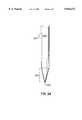
- FIG. 1shows a perspective view of a conventional tape automated bonding process, including a tape, its placement over an integrated circuit chip and a bonding tool;
- FIG. 2Ashows a magnified side cut-away view of a bonding tool according to a first embodiment of the present invention
- FIG. 2Bshows a greatly magnified view of an end tip surface of a bonding tool according to the first embodiment of the present invention
- FIG. 2Cshows a greatly magnified side cut-away view of the end tip of a bonding tool according to the first embodiment of the present invention
- FIG. 3Ashows a magnified side cut-away view of a bonding tool according to a second embodiment of the present invention
- FIG. 3Bshows a greatly magnified view of an end tip surface of a bonding tool according to the second embodiment of the present invention.
- FIG. 3Cshows a greatly magnified side cut-away view of the end tip of a bonding tool according to the second embodiment of the present invention.
- bonding tool 100made of substantially pure sintered aluminum oxide ceramic without metallic binders, according to a first embodiment of the present invention.
- bonding tool 100is made of 99.99% pure Al 2 O 3 , which is available by Small Precision Tools, 1330 Clegg Street, Petaluma, Calif., 94954.
- Bonding tool 100is comprised of a cylindrical shank body portion 102 having a diameter of approximately 0.0624 ⁇ 0.0001 inches and a conical end portion 104.
- bonding tool 100is approximately 0.470 ⁇ 0.005 inches.
- Conical end portion 104terminates at contact end surface 106, which has a diameter of approximately 0.004 ⁇ 0.0003/-0 inches.
- contact end surface 106comprises three substantially flat, inner contact regions 110 that are approximately 0.0004 inches wide and two substantially flat, outer contact regions 112 that are approximately 0.0002 inches wide.
- Contact regions 110 and 112are separated by grooves 108, which are approximately 0.0006 ⁇ 0.0001 inches wide and approximately 0.0003 ⁇ 0.0001 inches deep.
- an Aluminum Oxide (Alumina) ceramic, cylindrical blank with a tapered end portion 104is made by well known molding and sintering processes. The taper being at approximately a 30° included angle. Then the cylindrical blank is ground and lapped to form the final shape and size. The blank is then cut with a laser or diamond saw to the specified length. Next, grooves 108 are formed in contact end surface 106 using diamond saw or laser machining techniques. Also, as will be apparent to those of ordinary skill in the art, other hard materials, such as monocrystalline sapphire could be used for fabricating the bonding tool, as long as no metallic binders are used.
- bonding tool 200made of substantially pure sintered Aluminum Oxide ceramic without metallic binders, according to a second embodiment of the present invention, is shown.
- bonding tool 200is made of 99.99% pure Al 2 O 3 .
- Bonding tool 200is comprised of a cylindrical shank body portion 202 having a diameter of approximately 0.0624 ⁇ 0.0001 inches and a conical end portion 204. The entire length of bonding tool 200 is approximately 0.470 ⁇ 0.005 inches.
- Conical end portion 204terminates at contact end surface 206.
- contact end surface 206comprises a substantially flat contact ring 214 that has an outer diameter of approximately 0.0046 inches and an inner diameter of approximately 0.0042 inches.
- contact ring 214is a circular mesa structure having a height of approximately 0.0008 inches above a valley region 208, which has a diameter of approximately 0.0026 inches.
- an Aluminum Oxide (Alumina) ceramic, cylindrical shank with a tapered end portion 204is made by well known molding and sintering processes. The taper being at approximately a 30° included angle.
- the tapered end portion 204includes sloped wall 212, which is at approximately a 45° angle from the center axis XX. Then the cylindrical blank is ground and lapped to form the final shape and size. The shank is then cut with a laser or a diamond saw to the specified length. Valley region 208 in end portion 204 is formed using an ultrasonic machining process or a grinding process.
- This bonding toolis considered to be superior, because the contact end is omnidirectional. Therefore, the direction of the tool with regard to the direction of the device to be bonded is irrelevant. Accordingly, it is unnecessary to align the direction of the contact end mesa(s) to be perpendicular with the direction of the lead fingers, which would be necessary for bonding tools of the prior art and the first embodiment of the present invention.
- Such an alignment procedurerequires all of the lead fingers in one direction to be bonded and then the bonding tool must be realigned before the lead fingers in the opposite direction (or any other direction) can be bonded.
- the bonding tool of the present inventioncan be used in the same bonding machines and in the same manner that other bonding tools are used for TAB bonding--with two exceptions.
- the Alumina bonding tool of the present inventionhas a useful bonding life span of more than 500,000 bonds, in contradistinction with the useful life span of conventional bonding tools of just a few hundred bonds.
- the bonding tool of the second embodiment of the present inventiondoes not require the precise alignment with the lead fingers of the device to be bonded that bonding tools of the prior art require. It will be readily evident to one of ordinary skill in the art that the dimensions of the bonding tools will necessarily change with the intended use and the bonding machine to be used.
- the bonding tool of the present inventiondoes not have to be Aluminum Oxide ceramic, but can be any hard material, such as ruby or sapphire, so long as the binder material used is not nickel or any other material that is readily abraded by gold (usually metallic binder materials are readily abrated by gold).
- the teachings of the present inventionmay be used for bonding tools in wedge bonding with gold wire, where similar bonding tool wear problems exist.
Landscapes
- Engineering & Computer Science (AREA)
- Computer Hardware Design (AREA)
- Microelectronics & Electronic Packaging (AREA)
- Power Engineering (AREA)
- Mechanical Engineering (AREA)
- Manufacturing & Machinery (AREA)
- Wire Bonding (AREA)
Abstract
Description
Claims (6)
Priority Applications (3)
| Application Number | Priority Date | Filing Date | Title |
|---|---|---|---|
| US08/521,196US5816472A (en) | 1994-01-28 | 1995-08-30 | Bonding tool for tape automated assembly |
| GB9617052AGB2305001A (en) | 1995-08-30 | 1996-08-14 | Tool for tape automated bonding |
| JP8220249AJPH10308421A (en) | 1995-08-30 | 1996-08-22 | Tab device and method for manufacturing tab device |
Applications Claiming Priority (2)
| Application Number | Priority Date | Filing Date | Title |
|---|---|---|---|
| US18828294A | 1994-01-28 | 1994-01-28 | |
| US08/521,196US5816472A (en) | 1994-01-28 | 1995-08-30 | Bonding tool for tape automated assembly |
Related Parent Applications (1)
| Application Number | Title | Priority Date | Filing Date |
|---|---|---|---|
| US18828294AContinuation-In-Part | 1994-01-28 | 1994-01-28 |
Publications (1)
| Publication Number | Publication Date |
|---|---|
| US5816472Atrue US5816472A (en) | 1998-10-06 |
Family
ID=24075768
Family Applications (1)
| Application Number | Title | Priority Date | Filing Date |
|---|---|---|---|
| US08/521,196Expired - Fee RelatedUS5816472A (en) | 1994-01-28 | 1995-08-30 | Bonding tool for tape automated assembly |
Country Status (3)
| Country | Link |
|---|---|
| US (1) | US5816472A (en) |
| JP (1) | JPH10308421A (en) |
| GB (1) | GB2305001A (en) |
Cited By (33)
| Publication number | Priority date | Publication date | Assignee | Title |
|---|---|---|---|---|
| US6305074B1 (en)* | 1996-06-13 | 2001-10-23 | Bull, S.A. | Support for integrated circuit and process for mounting an integrated circuit on a support |
| US6354479B1 (en)* | 1999-02-25 | 2002-03-12 | Sjm Technologies | Dissipative ceramic bonding tip |
| WO2002087817A1 (en)* | 2001-05-01 | 2002-11-07 | Steven Frederick Reiber | Dissipative ceramic bonding tool tip |
| US6519500B1 (en) | 1999-09-16 | 2003-02-11 | Solidica, Inc. | Ultrasonic object consolidation |
| US20030150108A1 (en)* | 1998-09-09 | 2003-08-14 | Kazushi Higashi | Component mounting tool, and method and apparatus for mounting component using this tool |
| US20040149393A1 (en)* | 2002-11-01 | 2004-08-05 | Hickman Johnny M. | Welding tip |
| US6814823B1 (en) | 1999-09-16 | 2004-11-09 | Solidica, Inc. | Object consolidation through sequential material deposition |
| US20050087585A1 (en)* | 2003-10-23 | 2005-04-28 | Copperthite Theodore J. | Automated filament attachment system for vacuum fluorescent display |
| US20050109814A1 (en)* | 1999-02-25 | 2005-05-26 | Reiber Steven F. | Bonding tool with resistance |
| US20050242155A1 (en)* | 1999-02-25 | 2005-11-03 | Reiber Steven F | Flip chip bonding tool and ball placement capillary |
| US20060071050A1 (en)* | 1999-02-25 | 2006-04-06 | Reiber Steven F | Multi-head tab bonding tool |
| US20060163315A1 (en)* | 2005-01-27 | 2006-07-27 | Delsman Mark A | Ribbon bonding tool and process |
| US20060180635A1 (en)* | 2005-02-17 | 2006-08-17 | Oon-Pin Lim | Bonding tool and method |
| US20060261132A1 (en)* | 1999-02-25 | 2006-11-23 | Reiber Steven F | Low range bonding tool |
| US20070085085A1 (en)* | 2005-08-08 | 2007-04-19 | Reiber Steven F | Dissipative pick and place tools for light wire and LED displays |
| US20070131661A1 (en)* | 1999-02-25 | 2007-06-14 | Reiber Steven F | Solder ball placement system |
| US7389905B2 (en) | 1999-02-25 | 2008-06-24 | Reiber Steven F | Flip chip bonding tool tip |
| US20080197172A1 (en)* | 1999-02-25 | 2008-08-21 | Reiber Steven F | Bonding Tool |
| US20080236017A1 (en)* | 2007-01-11 | 2008-10-02 | Magpul Industries Corporation | Adjustable Cheek Piece for a Firearm Butt Stock |
| US7918378B1 (en)* | 2010-08-06 | 2011-04-05 | National Semiconductor Corporation | Wire bonding deflector for a wire bonder |
| US20120125520A1 (en)* | 2009-06-23 | 2012-05-24 | Toshiba Mitsubishi-Electric Industrial. Sys. Corp. | Ultrasonic bonding tool, method for manufacturing ultrasonic bonding tool, ultrasonic bonding method, and ultrasonic bonding apparatus |
| CN103219255A (en)* | 2013-03-15 | 2013-07-24 | 李尚哲 | An ultrasonic welding chopper with multiple welding wire slots |
| US20130193193A1 (en)* | 2012-01-27 | 2013-08-01 | Apple Inc. | Ultrasonic bonding |
| USD821468S1 (en)* | 2015-02-03 | 2018-06-26 | Coorstek, Inc. | Ceramic bonding tool with textured tip |
| US20180219345A1 (en)* | 2015-07-29 | 2018-08-02 | Telsonic Holding Ag | Sonotrode, device and method for producing a join |
| USD824969S1 (en) | 2015-02-03 | 2018-08-07 | Coorstek, Inc. | Ceramic bonding tool with textured tip |
| USD824970S1 (en) | 2015-02-03 | 2018-08-07 | Coorstek, Inc. | Ceramic bonding tool with textured tip |
| US20190009357A1 (en)* | 2017-07-06 | 2019-01-10 | Nippon Mektron, Ltd. | Ultrasonic bonding jig, bonding structure, and bonding method |
| USD868123S1 (en) | 2016-12-20 | 2019-11-26 | Coorstek, Inc. | Wire bonding wedge tool |
| US20210086290A1 (en)* | 2019-09-24 | 2021-03-25 | GM Global Technology Operations LLC | Apparatus for ultrasonic welding of polymers and polymeric composites |
| US20210111146A1 (en)* | 2019-10-10 | 2021-04-15 | Skyworks Solutions, Inc. | Cupd wire bond capillary design |
| US20220347786A1 (en)* | 2021-04-30 | 2022-11-03 | Infineon Technologies Ag | Ultrasonic welding device |
| US11929265B2 (en)* | 2021-12-21 | 2024-03-12 | Mitsubishi Electric Corporation | Semiconductor manufacturing apparatus and method of manufacturing semiconductor device |
Families Citing this family (2)
| Publication number | Priority date | Publication date | Assignee | Title |
|---|---|---|---|---|
| JP7325454B2 (en)* | 2019-01-28 | 2023-08-14 | 京セラ株式会社 | Bonding tool, manufacturing method thereof, bonding apparatus and bonding method |
| EP4371691A4 (en)* | 2022-09-27 | 2024-10-16 | Jiangsu Contemporary Amperex Technology Limited | WELDING BASE, WELDING UNIT AND ULTRASONIC WELDING MACHINE |
Citations (8)
| Publication number | Priority date | Publication date | Assignee | Title |
|---|---|---|---|---|
| US3750926A (en)* | 1971-03-02 | 1973-08-07 | Hitachi Ltd | Vibration element for supersonic bonding |
| US4030657A (en)* | 1972-12-26 | 1977-06-21 | Rca Corporation | Wire lead bonding tool |
| US4315128A (en)* | 1978-04-07 | 1982-02-09 | Kulicke And Soffa Industries Inc. | Electrically heated bonding tool for the manufacture of semiconductor devices |
| US4776509A (en)* | 1986-10-13 | 1988-10-11 | Microelectronics And Computer Technology Corporation | Single point bonding method and apparatus |
| US5147082A (en)* | 1987-08-17 | 1992-09-15 | Siemens Aktiengesellschaft | Tool configuration for ultrasonic welding |
| EP0506112A1 (en)* | 1991-03-27 | 1992-09-30 | Nec Corporation | Method of bonding TAB inner lead and bonding tool |
| US5180093A (en)* | 1991-09-05 | 1993-01-19 | Cray Research, Inc. | Apparatus for ultrasonic bonding |
| GB2285943A (en)* | 1994-01-28 | 1995-08-02 | Hewlett Packard Co | Bonding tool for electronic device |
- 1995
- 1995-08-30USUS08/521,196patent/US5816472A/ennot_activeExpired - Fee Related
- 1996
- 1996-08-14GBGB9617052Apatent/GB2305001A/ennot_activeWithdrawn
- 1996-08-22JPJP8220249Apatent/JPH10308421A/enactivePending
Patent Citations (8)
| Publication number | Priority date | Publication date | Assignee | Title |
|---|---|---|---|---|
| US3750926A (en)* | 1971-03-02 | 1973-08-07 | Hitachi Ltd | Vibration element for supersonic bonding |
| US4030657A (en)* | 1972-12-26 | 1977-06-21 | Rca Corporation | Wire lead bonding tool |
| US4315128A (en)* | 1978-04-07 | 1982-02-09 | Kulicke And Soffa Industries Inc. | Electrically heated bonding tool for the manufacture of semiconductor devices |
| US4776509A (en)* | 1986-10-13 | 1988-10-11 | Microelectronics And Computer Technology Corporation | Single point bonding method and apparatus |
| US5147082A (en)* | 1987-08-17 | 1992-09-15 | Siemens Aktiengesellschaft | Tool configuration for ultrasonic welding |
| EP0506112A1 (en)* | 1991-03-27 | 1992-09-30 | Nec Corporation | Method of bonding TAB inner lead and bonding tool |
| US5180093A (en)* | 1991-09-05 | 1993-01-19 | Cray Research, Inc. | Apparatus for ultrasonic bonding |
| GB2285943A (en)* | 1994-01-28 | 1995-08-02 | Hewlett Packard Co | Bonding tool for electronic device |
Non-Patent Citations (3)
| Title |
|---|
| Bonding Capillaries for Thermosonic or Thermocompression Gold Wire Bonding, Small Precision Tools, Petaluma, CA, 1988.* |
| M.K. Avedissian, "Multidirectional Ultransonic Wire Bonding Tip," Western Electric Tech. Dig., No. 20, Oct. 1970, pp. 7-8. |
| M.K. Avedissian, Multidirectional Ultransonic Wire Bonding Tip, Western Electric Tech. Dig., No. 20, Oct. 1970, pp. 7 8.* |
Cited By (59)
| Publication number | Priority date | Publication date | Assignee | Title |
|---|---|---|---|---|
| US6305074B1 (en)* | 1996-06-13 | 2001-10-23 | Bull, S.A. | Support for integrated circuit and process for mounting an integrated circuit on a support |
| US7549567B2 (en)* | 1998-09-09 | 2009-06-23 | Panasonic Corporation | Component mounting tool, and method and apparatus for mounting component using this tool |
| US20070119905A1 (en)* | 1998-09-09 | 2007-05-31 | Kazushi Higashi | Component mounting tool, and method and apparatus for mounting component using this tool |
| US7219419B2 (en) | 1998-09-09 | 2007-05-22 | Matsushita Electric Industrial Co., Ltd. | Component mounting apparatus including a polishing device |
| US20030150108A1 (en)* | 1998-09-09 | 2003-08-14 | Kazushi Higashi | Component mounting tool, and method and apparatus for mounting component using this tool |
| US20050242155A1 (en)* | 1999-02-25 | 2005-11-03 | Reiber Steven F | Flip chip bonding tool and ball placement capillary |
| US7032802B2 (en) | 1999-02-25 | 2006-04-25 | Reiber Steven F | Bonding tool with resistance |
| US20070131661A1 (en)* | 1999-02-25 | 2007-06-14 | Reiber Steven F | Solder ball placement system |
| US6354479B1 (en)* | 1999-02-25 | 2002-03-12 | Sjm Technologies | Dissipative ceramic bonding tip |
| US20060261132A1 (en)* | 1999-02-25 | 2006-11-23 | Reiber Steven F | Low range bonding tool |
| US20050109814A1 (en)* | 1999-02-25 | 2005-05-26 | Reiber Steven F. | Bonding tool with resistance |
| US6935548B2 (en)* | 1999-02-25 | 2005-08-30 | Steven-Frederick Reiber | Dissipative ceramic bonding tool tip |
| US7389905B2 (en) | 1999-02-25 | 2008-06-24 | Reiber Steven F | Flip chip bonding tool tip |
| US20060071050A1 (en)* | 1999-02-25 | 2006-04-06 | Reiber Steven F | Multi-head tab bonding tool |
| US20040046007A1 (en)* | 1999-02-25 | 2004-03-11 | Steven-Frederick Reiber | Dissipative ceramic bonding tool tip |
| US6651864B2 (en)* | 1999-02-25 | 2003-11-25 | Steven Frederick Reiber | Dissipative ceramic bonding tool tip |
| US20080197172A1 (en)* | 1999-02-25 | 2008-08-21 | Reiber Steven F | Bonding Tool |
| US7124927B2 (en) | 1999-02-25 | 2006-10-24 | Reiber Steven F | Flip chip bonding tool and ball placement capillary |
| US6519500B1 (en) | 1999-09-16 | 2003-02-11 | Solidica, Inc. | Ultrasonic object consolidation |
| US6814823B1 (en) | 1999-09-16 | 2004-11-09 | Solidica, Inc. | Object consolidation through sequential material deposition |
| WO2002087817A1 (en)* | 2001-05-01 | 2002-11-07 | Steven Frederick Reiber | Dissipative ceramic bonding tool tip |
| US7204289B2 (en) | 2002-11-01 | 2007-04-17 | Rieke Corporation | Welding tip |
| US20040149393A1 (en)* | 2002-11-01 | 2004-08-05 | Hickman Johnny M. | Welding tip |
| US20050087585A1 (en)* | 2003-10-23 | 2005-04-28 | Copperthite Theodore J. | Automated filament attachment system for vacuum fluorescent display |
| US7407079B2 (en)* | 2003-10-23 | 2008-08-05 | Orthodyne Electronics Corporation | Automated filament attachment system for vacuum fluorescent display |
| US20080193719A1 (en)* | 2005-01-27 | 2008-08-14 | Orthodyne Electronics Corporation | Ribbon bonding tool and process |
| WO2006081106A1 (en)* | 2005-01-27 | 2006-08-03 | Orthodyne Electronics Corporation | Ribbon bonding tool and process |
| US20060163315A1 (en)* | 2005-01-27 | 2006-07-27 | Delsman Mark A | Ribbon bonding tool and process |
| US20090297786A1 (en)* | 2005-01-27 | 2009-12-03 | Orthodyne Electronics Corporation | Ribbon bonding tool and process |
| US7838101B2 (en) | 2005-01-27 | 2010-11-23 | Orthodyne Electronics, Inc. | Ribbon bonding tool and process |
| US7909228B2 (en) | 2005-01-27 | 2011-03-22 | Orthodyne Electronics Corporation | Ribbon bonding tool and process |
| US7934633B2 (en) | 2005-01-27 | 2011-05-03 | Orthodyne Electronics Corporation | Ribbon bonding tool and process |
| US20060180635A1 (en)* | 2005-02-17 | 2006-08-17 | Oon-Pin Lim | Bonding tool and method |
| US20070085085A1 (en)* | 2005-08-08 | 2007-04-19 | Reiber Steven F | Dissipative pick and place tools for light wire and LED displays |
| US20080236017A1 (en)* | 2007-01-11 | 2008-10-02 | Magpul Industries Corporation | Adjustable Cheek Piece for a Firearm Butt Stock |
| US10864597B2 (en) | 2009-06-23 | 2020-12-15 | Toshiba Mitsubishi-Electric Industrial Systems Corporation | Ultrasonic bonding tool, method for manufacturing ultrasonic bonding tool, ultrasonic bonding method, and ultrasonic bonding apparatus |
| US20120125520A1 (en)* | 2009-06-23 | 2012-05-24 | Toshiba Mitsubishi-Electric Industrial. Sys. Corp. | Ultrasonic bonding tool, method for manufacturing ultrasonic bonding tool, ultrasonic bonding method, and ultrasonic bonding apparatus |
| US7918378B1 (en)* | 2010-08-06 | 2011-04-05 | National Semiconductor Corporation | Wire bonding deflector for a wire bonder |
| US8267303B2 (en)* | 2010-08-06 | 2012-09-18 | National Semiconductor Corporation | Wire bonding apparatus with a textured capillary surface enabling high-speed wedge bonding of wire bonds |
| US20130193193A1 (en)* | 2012-01-27 | 2013-08-01 | Apple Inc. | Ultrasonic bonding |
| US8800846B2 (en)* | 2012-01-27 | 2014-08-12 | Apple Inc. | Ultrasonic bonding |
| CN103219255A (en)* | 2013-03-15 | 2013-07-24 | 李尚哲 | An ultrasonic welding chopper with multiple welding wire slots |
| USD821468S1 (en)* | 2015-02-03 | 2018-06-26 | Coorstek, Inc. | Ceramic bonding tool with textured tip |
| USD824969S1 (en) | 2015-02-03 | 2018-08-07 | Coorstek, Inc. | Ceramic bonding tool with textured tip |
| USD824970S1 (en) | 2015-02-03 | 2018-08-07 | Coorstek, Inc. | Ceramic bonding tool with textured tip |
| US20180219345A1 (en)* | 2015-07-29 | 2018-08-02 | Telsonic Holding Ag | Sonotrode, device and method for producing a join |
| US10554004B2 (en)* | 2015-07-29 | 2020-02-04 | Telsonic Holding Ag | Sonotrode, device and method for producing a join |
| USD868123S1 (en) | 2016-12-20 | 2019-11-26 | Coorstek, Inc. | Wire bonding wedge tool |
| US10744591B2 (en)* | 2017-07-06 | 2020-08-18 | Nippon Mektron, Ltd. | Ultrasonic bonding jig, bonding structure, and bonding method |
| US20190009357A1 (en)* | 2017-07-06 | 2019-01-10 | Nippon Mektron, Ltd. | Ultrasonic bonding jig, bonding structure, and bonding method |
| US10981245B2 (en)* | 2019-09-24 | 2021-04-20 | GM Global Technology Operations LLC | Apparatus for ultrasonic welding of polymers and polymeric composites |
| US20210086290A1 (en)* | 2019-09-24 | 2021-03-25 | GM Global Technology Operations LLC | Apparatus for ultrasonic welding of polymers and polymeric composites |
| US20210111146A1 (en)* | 2019-10-10 | 2021-04-15 | Skyworks Solutions, Inc. | Cupd wire bond capillary design |
| US12308341B2 (en)* | 2019-10-10 | 2025-05-20 | Skyworks Solutions, Inc. | Wire bond capillary design |
| US20220347786A1 (en)* | 2021-04-30 | 2022-11-03 | Infineon Technologies Ag | Ultrasonic welding device |
| US11772187B2 (en)* | 2021-04-30 | 2023-10-03 | Infineon Technologies Ag | Ultrasonic welding device |
| US20230390859A1 (en)* | 2021-04-30 | 2023-12-07 | Infineon Technologies Ag | Ultrasonic welding device |
| US12109645B2 (en)* | 2021-04-30 | 2024-10-08 | Infineon Technologies Ag | Ultrasonic welding device |
| US11929265B2 (en)* | 2021-12-21 | 2024-03-12 | Mitsubishi Electric Corporation | Semiconductor manufacturing apparatus and method of manufacturing semiconductor device |
Also Published As
| Publication number | Publication date |
|---|---|
| JPH10308421A (en) | 1998-11-17 |
| GB2305001A (en) | 1997-03-26 |
| GB9617052D0 (en) | 1996-09-25 |
Similar Documents
| Publication | Publication Date | Title |
|---|---|---|
| US5816472A (en) | Bonding tool for tape automated assembly | |
| US7500590B2 (en) | Multi-part capillary | |
| US5217154A (en) | Semiconductor bonding tool | |
| KR100355974B1 (en) | Method and Apparatus for Fine Pitch Wire Bonding Using a Shaved Capillary | |
| JP3996216B2 (en) | Improved capillary and fine pitch ball bonding method | |
| US20030015567A1 (en) | Ultra fine pitch capillary | |
| US20010045443A1 (en) | Controlled attenuation capillary | |
| EP1189722B1 (en) | Efficient energy transfer capillary | |
| GB2285943A (en) | Bonding tool for electronic device | |
| JP2007535820A (en) | Low loop wire bonding systems and methods | |
| US4754912A (en) | Controlled collapse thermocompression gang bonding | |
| WO2003000454A1 (en) | Controlled attenuation capillary with planar surface | |
| JP2006512788A (en) | Capillary with internal bevel | |
| EP2167269B1 (en) | Wire bonding capillary tool having multiple outer steps | |
| JP2665062B2 (en) | Method for manufacturing semiconductor device | |
| JP2002231659A (en) | Method for manufacturing semiconductor device | |
| JPH0383613A (en) | How to divide the workpiece | |
| JP2780502B2 (en) | Array substrate of fine metal spheres and method of manufacturing the same | |
| JPH09148358A (en) | Capillary for wire bonding damage prevention | |
| JPS6188537A (en) | Semiconductor device leads | |
| TW202401537A (en) | SiC semiconductor device and method of manufacturing SiC semiconductor device | |
| CN114078797A (en) | Wire bonding for semiconductor devices | |
| JPS59200498A (en) | Die collet for assembling semiconductor device | |
| JPH04247950A (en) | Production of electrode | |
| JPS61125709A (en) | Pin chuck |
Legal Events
| Date | Code | Title | Description |
|---|---|---|---|
| AS | Assignment | Owner name:HEWLETT-PACKARD COMPANY, CALIFORNIA Free format text:ASSIGNMENT OF ASSIGNORS INTEREST;ASSIGNOR:LINN, LAWRENCE E.;REEL/FRAME:007831/0318 Effective date:19951019 | |
| AS | Assignment | Owner name:HEWLETT-PACKARD COMPANY, A DELAWARE CORPORATION, C Free format text:MERGER;ASSIGNOR:HEWLETT-PACKARD COMPANY, A CALIFORNIA CORPORATION;REEL/FRAME:010841/0649 Effective date:19980520 | |
| AS | Assignment | Owner name:AGILENT TECHNOLOGIES INC, CALIFORNIA Free format text:ASSIGNMENT OF ASSIGNORS INTEREST;ASSIGNOR:HEWLETT-PACKARD COMPANY;REEL/FRAME:010977/0540 Effective date:19991101 | |
| FEPP | Fee payment procedure | Free format text:PAYOR NUMBER ASSIGNED (ORIGINAL EVENT CODE: ASPN); ENTITY STATUS OF PATENT OWNER: LARGE ENTITY | |
| FPAY | Fee payment | Year of fee payment:4 | |
| REMI | Maintenance fee reminder mailed | ||
| AS | Assignment | Owner name:AVAGO TECHNOLOGIES GENERAL IP PTE. LTD., SINGAPORE Free format text:ASSIGNMENT OF ASSIGNORS INTEREST;ASSIGNOR:AGILENT TECHNOLOGIES, INC.;REEL/FRAME:017207/0020 Effective date:20051201 | |
| FPAY | Fee payment | Year of fee payment:8 | |
| REMI | Maintenance fee reminder mailed | ||
| LAPS | Lapse for failure to pay maintenance fees | ||
| STCH | Information on status: patent discontinuation | Free format text:PATENT EXPIRED DUE TO NONPAYMENT OF MAINTENANCE FEES UNDER 37 CFR 1.362 | |
| FP | Lapsed due to failure to pay maintenance fee | Effective date:20101006 | |
| AS | Assignment | Owner name:AVAGO TECHNOLOGIES GENERAL IP (SINGAPORE) PTE. LTD Free format text:CORRECTIVE ASSIGNMENT TO CORRECT THE NAME OF THE ASSIGNEE PREVIOUSLY RECORDED ON REEL 017207 FRAME 0020. ASSIGNOR(S) HEREBY CONFIRMS THE ASSIGNMENT;ASSIGNOR:AGILENT TECHNOLOGIES, INC.;REEL/FRAME:038633/0001 Effective date:20051201 |