US5815681A - Integrated network switching hub and bus structure - Google Patents
Integrated network switching hub and bus structureDownload PDFInfo
- Publication number
- US5815681A US5815681AUS08/651,118US65111896AUS5815681AUS 5815681 AUS5815681 AUS 5815681AUS 65111896 AUS65111896 AUS 65111896AUS 5815681 AUS5815681 AUS 5815681A
- Authority
- US
- United States
- Prior art keywords
- bus
- port
- data
- lines
- switching hub
- Prior art date
- Legal status (The legal status is an assumption and is not a legal conclusion. Google has not performed a legal analysis and makes no representation as to the accuracy of the status listed.)
- Expired - Fee Related
Links
- 238000004891communicationMethods0.000claimsdescription17
- 239000000872bufferSubstances0.000claimsdescription16
- 238000012546transferMethods0.000claimsdescription10
- 238000000034methodMethods0.000description15
- 238000001465metallisationMethods0.000description13
- 238000004519manufacturing processMethods0.000description12
- 229910052751metalInorganic materials0.000description12
- 239000002184metalSubstances0.000description12
- 230000008569processEffects0.000description8
- 239000000758substrateSubstances0.000description8
- 230000008901benefitEffects0.000description4
- 239000004020conductorSubstances0.000description4
- 230000002093peripheral effectEffects0.000description4
- 229920002120photoresistant polymerPolymers0.000description4
- 239000005380borophosphosilicate glassSubstances0.000description3
- 238000000151depositionMethods0.000description3
- CURLTUGMZLYLDI-UHFFFAOYSA-NCarbon dioxideChemical compoundO=C=OCURLTUGMZLYLDI-UHFFFAOYSA-N0.000description2
- VYPSYNLAJGMNEJ-UHFFFAOYSA-NSilicium dioxideChemical compoundO=[Si]=OVYPSYNLAJGMNEJ-UHFFFAOYSA-N0.000description2
- 238000006243chemical reactionMethods0.000description2
- 238000005229chemical vapour depositionMethods0.000description2
- 230000007423decreaseEffects0.000description2
- 238000010586diagramMethods0.000description2
- 238000005530etchingMethods0.000description2
- 239000003292glueSubstances0.000description2
- 150000004706metal oxidesChemical class0.000description2
- 238000001020plasma etchingMethods0.000description2
- 238000012545processingMethods0.000description2
- 239000004065semiconductorSubstances0.000description2
- 229910016570AlCuInorganic materials0.000description1
- UGFAIRIUMAVXCW-UHFFFAOYSA-NCarbon monoxideChemical compound[O+]#[C-]UGFAIRIUMAVXCW-UHFFFAOYSA-N0.000description1
- 229910052581Si3N4Inorganic materials0.000description1
- 229910052782aluminiumInorganic materials0.000description1
- XAGFODPZIPBFFR-UHFFFAOYSA-NaluminiumChemical compound[Al]XAGFODPZIPBFFR-UHFFFAOYSA-N0.000description1
- WPPDFTBPZNZZRP-UHFFFAOYSA-Naluminum copperChemical compound[Al].[Cu]WPPDFTBPZNZZRP-UHFFFAOYSA-N0.000description1
- -1aluminum silicon copperChemical compound0.000description1
- 238000004380ashingMethods0.000description1
- QVGXLLKOCUKJST-UHFFFAOYSA-Natomic oxygenChemical compound[O]QVGXLLKOCUKJST-UHFFFAOYSA-N0.000description1
- 230000015572biosynthetic processEffects0.000description1
- 230000003139buffering effectEffects0.000description1
- 229910002092carbon dioxideInorganic materials0.000description1
- 239000001569carbon dioxideSubstances0.000description1
- 229910002091carbon monoxideInorganic materials0.000description1
- 229910052681coesiteInorganic materials0.000description1
- 238000010276constructionMethods0.000description1
- 229910052906cristobaliteInorganic materials0.000description1
- 230000006378damageEffects0.000description1
- 230000003247decreasing effectEffects0.000description1
- 230000001934delayEffects0.000description1
- 230000008021depositionEffects0.000description1
- 239000003989dielectric materialSubstances0.000description1
- 238000009792diffusion processMethods0.000description1
- 230000000694effectsEffects0.000description1
- 239000000835fiberSubstances0.000description1
- 238000003384imaging methodMethods0.000description1
- 230000006872improvementEffects0.000description1
- 230000010354integrationEffects0.000description1
- 229910044991metal oxideInorganic materials0.000description1
- 229910052760oxygenInorganic materials0.000description1
- 239000001301oxygenSubstances0.000description1
- 230000037361pathwayEffects0.000description1
- 229910021420polycrystalline siliconInorganic materials0.000description1
- 229920001721polyimidePolymers0.000description1
- 229920005591polysiliconPolymers0.000description1
- 230000003252repetitive effectEffects0.000description1
- 230000004044responseEffects0.000description1
- 239000000377silicon dioxideSubstances0.000description1
- 235000012239silicon dioxideNutrition0.000description1
- 239000002904solventSubstances0.000description1
- 238000009987spinningMethods0.000description1
- 238000004544sputter depositionMethods0.000description1
- 229910052682stishoviteInorganic materials0.000description1
- 238000003860storageMethods0.000description1
- 239000000126substanceSubstances0.000description1
- 229910052905tridymiteInorganic materials0.000description1
- WFKWXMTUELFFGS-UHFFFAOYSA-NtungstenChemical compound[W]WFKWXMTUELFFGS-UHFFFAOYSA-N0.000description1
- 229910052721tungstenInorganic materials0.000description1
- 239000010937tungstenSubstances0.000description1
- XLYOFNOQVPJJNP-UHFFFAOYSA-NwaterSubstancesOXLYOFNOQVPJJNP-UHFFFAOYSA-N0.000description1
- 229910001868waterInorganic materials0.000description1
Images


Classifications
- H—ELECTRICITY
- H04—ELECTRIC COMMUNICATION TECHNIQUE
- H04L—TRANSMISSION OF DIGITAL INFORMATION, e.g. TELEGRAPHIC COMMUNICATION
- H04L49/00—Packet switching elements
- H04L49/25—Routing or path finding in a switch fabric
- H04L49/253—Routing or path finding in a switch fabric using establishment or release of connections between ports
- H04L49/254—Centralised controller, i.e. arbitration or scheduling
- H—ELECTRICITY
- H04—ELECTRIC COMMUNICATION TECHNIQUE
- H04L—TRANSMISSION OF DIGITAL INFORMATION, e.g. TELEGRAPHIC COMMUNICATION
- H04L49/00—Packet switching elements
- H04L49/35—Switches specially adapted for specific applications
- H04L49/351—Switches specially adapted for specific applications for local area network [LAN], e.g. Ethernet switches
- H—ELECTRICITY
- H04—ELECTRIC COMMUNICATION TECHNIQUE
- H04L—TRANSMISSION OF DIGITAL INFORMATION, e.g. TELEGRAPHIC COMMUNICATION
- H04L49/00—Packet switching elements
- H04L49/30—Peripheral units, e.g. input or output ports
- H04L49/3027—Output queuing
Definitions
- This inventionrelates generally to computer networks.
- itpertains to a relatively low cost network switching hub and bus structure integrated into an integrated circuit chip, which improves network performance by increasing bandwidth and reducing collisions.
- PCsPersonal computers
- Computer networksare becoming increasingly popular in low-cost, performance-oriented computing environments.
- LANlocal area network
- LANs and other types of networkspermit the sharing of resources such as software, printers, modems, and other peripherals among PC workstations operating as nodes on the network.
- FIG. 1illustrates a simple and conventional LAN, generally designated by the reference numeral 100.
- Network 100comprises a plurality of PC workstations 112a through 112e, each connected by a communication link 113a through 113e respectively to an associated hub 114.
- Communication links in such networksare typically two-conductor cables, wherein a potential across the two conductors is varied in a manner representing sequential binary data. Such a link is termed a serial link.
- Hubssuch as hub 114, in networks are used to connect multiple workstations for routing through a single link to a server.
- PC workstations 112a through 112eare all connected to server 116 through link 115.
- Hubstypically have a limited number of input ports, so the number of workstations that can be connected is limited as well. Typically the input ports are arranged in groups of 8, 16, 32, 64 and so forth. Further network capacity can be added by connecting multiple hubs, such as hub 118 (shown in dashed lines) to the one file server, and the additional hubs may then be connected to other multiple workstations (not shown).
- Other network variationsinclude addition of multiple file servers connected in different arrangements to multiple hubs.
- File server 116 in this examplecomprises a set of sheared high-capacity mass storage devices, such as hard disks.
- Such file serversare often special PCs that have higher performance capability and more and larger capacity hard disks than do individual workstations 112a through 112e.
- the shared disk space on such file serverstypically stores software applications which spreads the cost of the hard disk over more than one user, thereby permitting more efficient use of resources.
- File server 116 in this examplemay also contain routers (not shown) for communication and connection to different network protocols such as EthernetTM, Asynchronous Transfer Mode (ATM), and Fiber Distributed Data Interface (FDDI), among others.
- the output of file server 116is coupled to shared peripherals such as a network modem 118, a laser printer 120, and other peripherals represented by element number 122. All workstations 112a through 112e on the network share access to the peripherals connected to server 116.
- FIG. 1is but one of many network arrangements known in the art.
- a conventional LAN 100there are some limitations of a conventional LAN 100 as described above.
- communication over link 115is shared by all of the workstations, and if many workstations are attempting to communicate at once, bandwidth may be a problem, slowing communication.
- coaxial lines used in many networkshave a maximum data transfer rate of 10 megabytes per second (Mb/s).
- Mb/smegabytes per second
- the maximum data transfer ratewhich is related to bandwidth, ultimately determines the maximum number of workstations that can be adequately handled by the network.
- Overloading a networkcan result in lost connections, communication delays, slow system response, timeouts, and slow file transfer times. All of these situations decreases the efficiency of the network, and become very annoying to network users.
- LAN 100Another limitation of conventional LANs such as LAN 100, is that communication collisions may occur between multiple workstations requesting access to the network.
- network protocolssuch as EthernetTM
- one way that collisions are handledis by processing one request at-a-time while buffering other requests in a first-in-first-out (FIFO) buffer. Since access is granted one-workstation-at-a time, other stations are required to wait, thereby decreasing efficiency. Networks with heavy traffic tend to have many collisions which may drop efficiency to unacceptable levels.
- Another way to add bandwidthis by increasing the number of switching hubs. This solution often results in segmenting a single large network into multiple smaller networks, which decreases the amount of traffic that travels over any given communication link and thereby increases the bandwidth available to each individual user. Statistics and traffic patterns can be further analyzed for adjustments for optimal network performance.
- Another disadvantage of conventional networksis the relatively high cost of multi-port hubs.
- a 32 or even 16 port hub for some networkscan cost in the range of about 32K to 100K dollars, a substantial investment for any user.
- conventional hubsare typically separate units in an enclosure with a dedicated power supply and controlling electronics, adding to clutter and adding to cost.
- an integrated circuit (IC) switching hubcomprising a parallel bus of n bus lines implemented as traces on the IC; a first data port adapter controller connected by n first port lines through a first output buffer to the bus, each first port line connected to a bus line source-to-drain through one of a set of first queue switch transistors, and connected to a first data port providing a first external data link for the switching hub; a first read amplifier connected by n first receiver lines one each directly to each one of the n bus lines, and by a first data link to the first port adapter controller; a second data port adapter controller connected by n second port lines through a second output buffer to the bus, each second port line connected to a bus line source-to-drain through one of a set of second queue switch transistors, and connected to a second data port providing a second external data link for the switching hub; a second read amplifier connected by n second receiver lines one each directly to each one of the n bus lines and by a second data link
- the arbitrator controlleris adapted to switch data from the first and second port adapter controllers onto the bus through the first and second output buffers and the first and second sets of queue switch transistors by switching the gates of the transistors via the first and second control lines respectively, and adapted to transfer data from the bus to the first and second external data links via the first and second read amplifiers through the first and second port adapter controllers by enabling the respective port adapter controllers via the third and fourth control lines respectively, according to a preprogrammed arbitration scheme.
- the first and second port adapter controllersshare a single read amplifier, the read amplifier being connected to both port adapter controllers via a single data link.
- Portsmay be of any convenient nature, such a serial ports configured for network communication according to a standard protocol, such as EthernetTM. Ports also may be of another sort, such as a PCI parallel port adapted for communication with a PCI bus, or an expansion port adapted for connection to a similar switching hub.
- the IC switching hub in embodiments of the inventionprovides an ability to switch multiple packets without queuing and provides also greatly expanded band width for switching hubs, whereby, in some embodiments, cross traffic may be allowed without contention, depending on source and destination.
- the hub of the inventionfurthermore, is much more compact than prior art hubs, and by far less expensive than prior art hubs.
- FIG. 1is a block diagram of a conventional LAN network
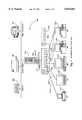
- FIG. 2is diagrammatical plan view of an integrated network switching hub and bus structure according to an embodiment of the present invention.
- FIG. 3is a perspective view of an integrated circuit die according to an of the embodiment of the present invention.
- FIG. 2is a diagrammatical plan view of an integrated switching hub and bus structure chip according to a preferred embodiment of the present invention. For purposes of illustration, a four conductor bus is shown including components and connections made in accordance to the invention.
- the purpose of the switching hubis to facilitate data transfer between devices connected to the hub.
- the connectionsare serial ports.
- Other sorts of portsmay be incorporated, however.
- the architecture of the hub according to embodiments of the present inventionis quite regular and repetitive. For this reason description of ports and data transfers is related herein to port units of two ports each.
- port units 210, 250 and 260are shown in detail. There may be more units with substantially the same structure, but not shown to keep the diagram as simple as possible. If the bus has a width of sixteen conductors, for example, there could be 16 or even 32 units like units 210, 250, and 260 illustrated.
- each port unithas two Medium Adapter Controllers (MACs), two output buffer transmitters, and access to two read amplifier receivers, all interconnected in a manner to be described below.
- MACsMedium Adapter Controllers
- Receivers 232 and 234are shared between unit 210 and unit 250 as is described more fully below.
- a network linkis connected to MAC 212 at port 211b.
- thisis link 113b of FIG. 1.
- a different numerical nomenclatureis used in this example simply because, in many networks, there is other hardware not shown between the port and the carrier line.
- the lines 113a-113eare connected to the ports 211a211e of the hub of FIG. 2. It will be apparent to those with skill in the art, however, that there is a broad variety of links that may be connected at this point. In the example given, any one of the links of FIG. 1 may be connected at any port of the hub of FIG. 2.
- MAC 212attaches to data layers of protocol to conform to the standard being used, for example, American National Standards Institute (ANSI), or Industrial Electrical Electronic Engineers (IEEE) standards.
- Datais transmitted from MAC 212 through bus 214 to transmitter 216 which mainly buffers the data always onto the four lines 217, 218, 219, and 220, each connecting via a switch 221, 222, 223 and 224 respectively to an associated bus line of bus 230.
- ANSIAmerican National Standards Institute
- IEEEIndustrial Electrical Electronic Engineers
- Switches 221 through 224are queue switch transistors. Such transistors are very fast (subnanoseconds) switching metal oxide (MOS) transistors.
- MOSmetal oxide
- Lines 217, 218, 219, and 220are coupled to the sources of transistors 221, 222, 223, and 224 respectively.
- the drains of transistors 221, 222, 223, and 224are coupled to bus lines 225, 226, 227, and 228 respectively, thereby creating a pathway for data from lines 217, 218, 219, and 220 to reach the bus through the transistors.
- transistors 221, 222, 223, and 224are coupled together as shown in FIG. 2 by a common line 255 to allow simultaneous enablement of the transistors, which allows data from transmitter 216 onto bus 230 with all bits being transferred simultaneously.
- Data present on bus 230is capable of being read by all receivers, such as receivers 232 and 234, since all receivers are connected directly to bus 230 as shown.
- Datais typically transferred in the form of packets containing at least two parts: (a) routing information, and (b) the data.
- the routing informationtells the MACs with the help of an arbitrator 244 via buses such as buses 248 and 246 and others where the data should go.
- Receiverssuch as receiver 232, are always enabled to receive data present on the bus. Since each of the receivers of the other modules are coupled directly to bus 230 as well, only a MAC enabled by the arbitrator will receive the data on bus 230 via its receiver.
- Data from receiver 232is in communication with a data register (not shown) which is controlled by MAC 233.
- MAC 233is further connected to line drivers and filters not shown.
- each of the lines of bus 230is connected to an associated line to an output buffer 236 via individual queue switch transistors 238, 239, 240, and 241.
- Data from output buffer (transmitter) 236is transmitted to a data register for output to MAC 233.
- Queue switch transistors 238, 239, 240, and 241are controlled by arbitrator 244 simultaneously via a common line 256, and thus the data flow to output buffer 236 can be controlled.
- arbitrator 244is coupled to enable all receiving functions through the medium adapter controllers. For example, even though read amplifier 232 is always enabled to receive data on the bus, as described above, this data is retrieved by enabling MAC 233 to read the data from receiver 232 to which the MAC is connected.
- Arbitrator 244is of critical importance to functions of the system in embodiments of the invention because of its role in directing the path of the data. Since all of the receivers are connected to bus 230 and are always enabled, data from any receiver can be retrieved by enabling an appropriate connected adpater controller by the arbitrator. It will be apparent to those with skill in the art that only one reciver would be sufficient for the system described, if that receiver were to be appropriately connected to each adapter controller. The sheer size of hubs in practical embodiments, having mant ports and therefore many port adapter controllers, makes connecting all adapter controllers to a single, or even to a few receivers is impractical. The scheme shown and described of sharing a receiver between sets of two ports is examplary and geometrically desirable for construction of such hubs, as is described more fully below.
- a communication line 248 from MAC 212 to arbitrator 244tells the arbitrator that data from a particular unit has been put on the bus. The arbitrator uses this information to select the appropriate receiver to retrieve the data. All MACs at net connections are in communication in this way with arbitrator 244, thereby permitting the arbitrator to determine which receiver should receive the data, according to a predetermined selection scheme.
- the selection (arbitration) schememay be changed remotely through input to arbitrator 244, and the particular arbitration scheme is not limiting to the invention.
- an arbitration scheme of selecting a receiver according to low frequency of usemay be changed to select receivers according to high frequency of use. This can be accomplished by toggling an input line to arbitrator 244 to activate internal circuitry to follow a particular selection scheme.
- MACsnot all MACs have to be for the same topology and bus speed.
- one of the MACs(253) could support a GIGAlink or similar type of high-band-width link.
- a major feature providing a major advantage for the above-described apparatus and technique over conventional systemsis that collisions are avoided since the queue transistors switch substantially faster than the incoming data rate from the Ethernet network.
- the switching hubresults in an immediate improvement in network performance.
- the prior art method of simply routing requests through a FIFO bufferrequires queued requests to wait, yielding inefficient performance during times of heavy network activity.
- Another major advantage of the present inventionis that the layout described above and shown in FIG. 2 may be efficiently incorporated into a single integrated circuit chip.
- the current method of semiconductor fabrication using multi-layer metalizationis exploited in embodiments of the present invention by fabricating portions of the layout on different metal layers in the chip.
- the queue switch transistorssuch as transistors 221, 222, 223, 224 and 238, 239, 240, 241 of FIG. 2 are fabricated in the first metalization layer, often referred to as metal-1, and bus structure 230 is fabricated in another metalization layer such as metal-2.
- the queue switch transistorsmay be conveniently positioned in the substrate to be underneath the bus structure in the metal layers in such a way that each transistor is connected to the appropriate associated bus line by a vertical via.
- Lines 217, 218, 219, and 220 from transmitter 216, enable lines 246, queue switch enable lines, and communication lines 248reside on another metal layer in the chip.
- the metal layersare electrically connected with tungsten contacts through vias etched in the dielectric layer. Connecting multi-metalization layers in semiconductor chips with contacts formed through etched vias in the dielectric is well known to those skilled in the art.
- the topological layout of the bus structure and interconnection linespermits convenient integration into one low-cost chip as opposed to requiring separate components as in the prior art.
- FIG. 3is a perspective illustration of an integrated circuit chip 300 in accordance with an embodiment of the present invention.
- the interconnection lines that electrically connect the queue switch transistors, arbitrator, MAC, receivers, transmitters, read amplifier etc.are fabricated into a first metalization layer 310 (sometimes referred to as metal-1).
- a dielectric layer 320is then overlaid over the metal-1 layer to prevent contact between the metal layers.
- a second metalization layer 330metal-2 is formed, and the bus structure is fabricated into metal-2. Connections between the substrate and various metal layers are made with contacts as described above.
- a brief description of a typical multi-metalization fabrication processfollows to illustrate a possible fabrication method for the present invention.
- the fabrication of a multi-metalization integrated circuitstarts with the fabrication of the substrate itself, which is done in a sequential set of processes often referred to in the IC fabrication art as the front end processes.
- Back end processinginvolves manufacture of finished functional ICs by further fabrication steps. It is often useful to split fabrication in this way because many customers of a substrate manufacturer use the same substrates to fabricate their own ICs.
- the front end processesare relatively unimportant for illustrating embodiments of the present invention, whereas the back end processes will be the focus of the impending discussion.
- the processbegins with a contact mask and a contact etch applied over the polysilicon substrate.
- An optional step of depositing a glue layer prior to metal depositionis performed to function as a diffusion layer between the metal and the substrate. This is followed by a blanket deposition of a metal-1 layer which is deposited on top of the glue layer.
- the metal layermay be of any suitable metal used in the industry such as aluminum (Al), aluminum copper (AlCu), or aluminum silicon copper (AlSiCu), and is deposited by a method such as chemical vapor deposition (CVD), which is well known in the industry.
- an etching step of the of the metal-1 layeris performed such that interconnection lines are formed in the metal-1 layer that will connect to the queue switch transistors.
- Etchingis then done by first depositing a mask, such as a photoresist layer, which becomes cured and insoluble upon exposure to light and thereby cannot be washed away by solvents.
- a masksuch as a photoresist layer
- Such masksare known as a negative resists since the areas not covered by the mask are etched away.
- the metal-1 layeris etched by a plasma process such as sputtering or reactive ion etching (RIE) to form the interconnection lines.
- RIEreactive ion etching
- the photoresistis removed, which can be done by a variety of dry and wet chemical etches.
- Plasma removal of the photoresistcan be performed and is known as plasma ashing. This is done by placing the substrates in a tunnel reactor in the presence of an oxygen plasma which triggers reactions that oxidize the resist. The reaction produces a combination of water, carbon monoxide, and carbon dioxide which are quickly desorbed.
- a dielectric layeris deposited over the metal-1 layer in order to insulate the metal-1 layer from the next metal layer (metal-2).
- metal-1metal layer
- metal-2metal layer
- BPSGborophosphosilicate glass
- BPSGborophosphosilicate glass
- Other dielectricssuch as Si3N4 and polyimide films which can be laid on by spinning may be used.
- a via maskis then deposited on the dielectric layer leaving via patterns for exposure to an etchant to form vias (holes) in the dielectric through which interconnection of structure on the metal layers may be accomplished.
- the next metalization layer(metal-2) is deposited and the above steps are repeated until a final metalization layer (as many as metal-3 or metal-4) is reached.
- the fabrication of the top metalization layerincludes metal bond pads for attachment to bonding wires that are attached to the lead frame of an IC package, providing interconnection to the outside world.
- the present inventionin various embodiments provides a low cost network switching hub (in the hundreds of dollars) in a small integrated circuit chip that can be mounted on an associated circuit board which can be installed in a file server. Another advantage is that the present invention consumes less power, produces less noise, and provides faster performance than prior art hubs.
Landscapes
- Engineering & Computer Science (AREA)
- Computer Networks & Wireless Communication (AREA)
- Signal Processing (AREA)
- Small-Scale Networks (AREA)
Abstract
Description
Claims (7)
Priority Applications (6)
| Application Number | Priority Date | Filing Date | Title |
|---|---|---|---|
| US08/651,118US5815681A (en) | 1996-05-21 | 1996-05-21 | Integrated network switching hub and bus structure |
| PCT/US1997/008600WO1997044938A1 (en) | 1996-05-21 | 1997-05-20 | Integrated network switching hub and bus structure |
| US09/115,409US6226705B1 (en) | 1996-05-21 | 1998-07-14 | Integrated network switching hub and bus structure |
| US09/778,173US6493786B2 (en) | 1996-05-21 | 2001-02-06 | Integrated network switching hub and bus structure |
| US10/300,515US6678778B2 (en) | 1996-05-21 | 2002-11-20 | Integrated network switching hub and bus structure |
| US10/706,678US7020735B2 (en) | 1996-05-21 | 2003-11-12 | Integrated network switching hub and bus structure |
Applications Claiming Priority (1)
| Application Number | Priority Date | Filing Date | Title |
|---|---|---|---|
| US08/651,118US5815681A (en) | 1996-05-21 | 1996-05-21 | Integrated network switching hub and bus structure |
Related Child Applications (1)
| Application Number | Title | Priority Date | Filing Date |
|---|---|---|---|
| US09/115,409DivisionUS6226705B1 (en) | 1996-05-21 | 1998-07-14 | Integrated network switching hub and bus structure |
Publications (1)
| Publication Number | Publication Date |
|---|---|
| US5815681Atrue US5815681A (en) | 1998-09-29 |
Family
ID=24611643
Family Applications (5)
| Application Number | Title | Priority Date | Filing Date |
|---|---|---|---|
| US08/651,118Expired - Fee RelatedUS5815681A (en) | 1996-05-21 | 1996-05-21 | Integrated network switching hub and bus structure |
| US09/115,409Expired - Fee RelatedUS6226705B1 (en) | 1996-05-21 | 1998-07-14 | Integrated network switching hub and bus structure |
| US09/778,173Expired - Fee RelatedUS6493786B2 (en) | 1996-05-21 | 2001-02-06 | Integrated network switching hub and bus structure |
| US10/300,515Expired - Fee RelatedUS6678778B2 (en) | 1996-05-21 | 2002-11-20 | Integrated network switching hub and bus structure |
| US10/706,678Expired - Fee RelatedUS7020735B2 (en) | 1996-05-21 | 2003-11-12 | Integrated network switching hub and bus structure |
Family Applications After (4)
| Application Number | Title | Priority Date | Filing Date |
|---|---|---|---|
| US09/115,409Expired - Fee RelatedUS6226705B1 (en) | 1996-05-21 | 1998-07-14 | Integrated network switching hub and bus structure |
| US09/778,173Expired - Fee RelatedUS6493786B2 (en) | 1996-05-21 | 2001-02-06 | Integrated network switching hub and bus structure |
| US10/300,515Expired - Fee RelatedUS6678778B2 (en) | 1996-05-21 | 2002-11-20 | Integrated network switching hub and bus structure |
| US10/706,678Expired - Fee RelatedUS7020735B2 (en) | 1996-05-21 | 2003-11-12 | Integrated network switching hub and bus structure |
Country Status (2)
| Country | Link |
|---|---|
| US (5) | US5815681A (en) |
| WO (1) | WO1997044938A1 (en) |
Cited By (21)
| Publication number | Priority date | Publication date | Assignee | Title |
|---|---|---|---|---|
| WO1999053404A1 (en)* | 1998-04-09 | 1999-10-21 | Novaweb Technologies, Inc. | Integrated apparatus for interfacing several computers to the internet through a single connection |
| US6052751A (en)* | 1997-02-14 | 2000-04-18 | Advanced Micro Devices, I Nc. | Method and apparatus for changing the number of access slots into a memory |
| US6226705B1 (en)* | 1996-05-21 | 2001-05-01 | Elonex Plc | Integrated network switching hub and bus structure |
| US20030147984A1 (en)* | 2002-02-07 | 2003-08-07 | Krauss-Maffei Kunststofftechnik Gmbh, | Injection molding machine with control system |
| US6718415B1 (en)* | 1999-05-14 | 2004-04-06 | Acqis Technology, Inc. | Computer system and method including console housing multiple computer modules having independent processing units, mass storage devices, and graphics controllers |
| US20050213496A1 (en)* | 2000-09-21 | 2005-09-29 | Serconet, Ltd | Telephone communication system and method over local area network wiring |
| US20070033507A1 (en)* | 2005-08-03 | 2007-02-08 | Xueping Jiang | Efficient error code correction |
| US20070091915A1 (en)* | 2000-04-19 | 2007-04-26 | Serconet Ltd. | Network combining wired and non wired segments |
| US7317793B2 (en) | 2003-01-30 | 2008-01-08 | Serconet Ltd | Method and system for providing DC power on local telephone lines |
| US7424031B2 (en) | 1998-07-28 | 2008-09-09 | Serconet, Ltd. | Local area network of serial intelligent cells |
| US7483524B2 (en) | 1999-07-20 | 2009-01-27 | Serconet, Ltd | Network for telephony and data communication |
| US7522714B2 (en) | 2000-03-20 | 2009-04-21 | Serconet Ltd. | Telephone outlet for implementing a local area network over telephone lines and a local area network using such outlets |
| US7522615B2 (en) | 2002-11-13 | 2009-04-21 | Serconet, Ltd. | Addressable outlet, and a network using same |
| USRE41076E1 (en) | 1998-10-30 | 2010-01-12 | Acqis Technology, Inc. | Password protected modular computer method and device |
| USRE41092E1 (en) | 1999-05-14 | 2010-01-26 | Acqis Technology, Inc. | Data security method and device for computer modules |
| US7756268B2 (en) | 2004-02-16 | 2010-07-13 | Mosaid Technologies Incorporated | Outlet add-on module |
| US7835386B2 (en) | 1999-07-07 | 2010-11-16 | Mosaid Technologies Incorporated | Local area network for distributing data communication, sensing and control signals |
| US7867035B2 (en) | 2003-07-09 | 2011-01-11 | Mosaid Technologies Incorporated | Modular outlet |
| US8671153B1 (en) | 2010-08-20 | 2014-03-11 | Acqis Llc | Low cost, high performance and high data throughput server blade |
| USRE48365E1 (en) | 2006-12-19 | 2020-12-22 | Mobile Motherboard Inc. | Mobile motherboard |
| US10986164B2 (en) | 2004-01-13 | 2021-04-20 | May Patents Ltd. | Information device |
Families Citing this family (13)
| Publication number | Priority date | Publication date | Assignee | Title |
|---|---|---|---|---|
| US7012896B1 (en)* | 1998-04-20 | 2006-03-14 | Alcatel | Dedicated bandwidth data communication switch backplane |
| US6314106B1 (en) | 1998-04-20 | 2001-11-06 | Alcatel Internetworking, Inc. | Receive processing for dedicated bandwidth data communication switch backplane |
| US6950893B2 (en)* | 2001-03-22 | 2005-09-27 | I-Bus Corporation | Hybrid switching architecture |
| US7103760B1 (en)* | 2001-07-16 | 2006-09-05 | Billington Corey A | Embedded electronic device connectivity system |
| US20040059862A1 (en)* | 2002-09-24 | 2004-03-25 | I-Bus Corporation | Method and apparatus for providing redundant bus control |
| US8923307B2 (en)* | 2003-07-14 | 2014-12-30 | Broadcom Corporation | Method and system for an integrated dual port gigabit ethernet controller chip |
| US7257683B2 (en)* | 2004-03-24 | 2007-08-14 | Micron Technology, Inc. | Memory arbitration system and method having an arbitration packet protocol |
| US7669057B2 (en)* | 2005-01-24 | 2010-02-23 | International Business Machines Corporation | Secure computer password system and method |
| US7814253B2 (en)* | 2007-04-16 | 2010-10-12 | Nvidia Corporation | Resource arbiter |
| US8005444B2 (en)* | 2007-08-02 | 2011-08-23 | Broadcom Corporation | Multiple die integrated circuit assembly |
| US7673087B1 (en)* | 2008-03-27 | 2010-03-02 | Xilinx, Inc. | Arbitration for an embedded processor block core in an integrated circuit |
| US8649262B2 (en)* | 2008-09-30 | 2014-02-11 | Intel Corporation | Dynamic configuration of potential links between processing elements |
| CN115695071B (en)* | 2022-09-27 | 2024-10-22 | 上海创贤半导体有限公司 | Bus communication system of power semiconductor wire bonding machine |
Citations (1)
| Publication number | Priority date | Publication date | Assignee | Title |
|---|---|---|---|---|
| US5546385A (en)* | 1995-01-19 | 1996-08-13 | Intel Corporation | Flexible switching hub for a communication network |
Family Cites Families (7)
| Publication number | Priority date | Publication date | Assignee | Title |
|---|---|---|---|---|
| US4787082A (en)* | 1986-07-24 | 1988-11-22 | American Telephone And Telegraph Company, At&T Bell Laboratories | Data flow control arrangement for local area network |
| US5345447A (en)* | 1993-02-05 | 1994-09-06 | Bytex Corporation | Switching hub which implements a virtual bus for interconnecting stations on a CSMA network |
| US6185222B1 (en)* | 1995-09-28 | 2001-02-06 | Cisco Technology, Inc. | Asymmetric switch architecture for use in a network switch node |
| US5991296A (en)* | 1996-02-22 | 1999-11-23 | Fujitsu, Ltd. | Crossbar switch and method with reduced voltage swing and no internal blocking data path |
| US5815681A (en)* | 1996-05-21 | 1998-09-29 | Elonex Plc Ltd. | Integrated network switching hub and bus structure |
| JP3545570B2 (en)* | 1997-03-18 | 2004-07-21 | 富士通株式会社 | Switching hub |
| US6069897A (en)* | 1997-07-09 | 2000-05-30 | Compaq Computer Corporation | Interface with dual mode of operation |
- 1996
- 1996-05-21USUS08/651,118patent/US5815681A/ennot_activeExpired - Fee Related
- 1997
- 1997-05-20WOPCT/US1997/008600patent/WO1997044938A1/enactiveApplication Filing
- 1998
- 1998-07-14USUS09/115,409patent/US6226705B1/ennot_activeExpired - Fee Related
- 2001
- 2001-02-06USUS09/778,173patent/US6493786B2/ennot_activeExpired - Fee Related
- 2002
- 2002-11-20USUS10/300,515patent/US6678778B2/ennot_activeExpired - Fee Related
- 2003
- 2003-11-12USUS10/706,678patent/US7020735B2/ennot_activeExpired - Fee Related
Patent Citations (1)
| Publication number | Priority date | Publication date | Assignee | Title |
|---|---|---|---|---|
| US5546385A (en)* | 1995-01-19 | 1996-08-13 | Intel Corporation | Flexible switching hub for a communication network |
Cited By (112)
| Publication number | Priority date | Publication date | Assignee | Title |
|---|---|---|---|---|
| US20040105397A1 (en)* | 1996-05-21 | 2004-06-03 | Elonex Ip Holdings Ltd. | Integrated network switching hub and bus structure |
| US6226705B1 (en)* | 1996-05-21 | 2001-05-01 | Elonex Plc | Integrated network switching hub and bus structure |
| US6493786B2 (en)* | 1996-05-21 | 2002-12-10 | Elonex Ip Holdings, Ld. | Integrated network switching hub and bus structure |
| US7020735B2 (en) | 1996-05-21 | 2006-03-28 | Elonex Ip Holdings Ltd. | Integrated network switching hub and bus structure |
| US6678778B2 (en) | 1996-05-21 | 2004-01-13 | Elonex Ip Holdings Ltd | Integrated network switching hub and bus structure |
| US6052751A (en)* | 1997-02-14 | 2000-04-18 | Advanced Micro Devices, I Nc. | Method and apparatus for changing the number of access slots into a memory |
| US6115755A (en)* | 1998-04-09 | 2000-09-05 | Novaweb Technologies, Inc. | Integrated apparatus for interfacing several computers to the internet through a single connection |
| WO1999053404A1 (en)* | 1998-04-09 | 1999-10-21 | Novaweb Technologies, Inc. | Integrated apparatus for interfacing several computers to the internet through a single connection |
| US8270430B2 (en) | 1998-07-28 | 2012-09-18 | Mosaid Technologies Incorporated | Local area network of serial intelligent cells |
| US7965735B2 (en) | 1998-07-28 | 2011-06-21 | Mosaid Technologies Incorporated | Local area network of serial intelligent cells |
| US8867523B2 (en) | 1998-07-28 | 2014-10-21 | Conversant Intellectual Property Management Incorporated | Local area network of serial intelligent cells |
| US7653015B2 (en) | 1998-07-28 | 2010-01-26 | Mosaid Technologies Incorporated | Local area network of serial intelligent cells |
| US8885659B2 (en) | 1998-07-28 | 2014-11-11 | Conversant Intellectual Property Management Incorporated | Local area network of serial intelligent cells |
| US8325636B2 (en) | 1998-07-28 | 2012-12-04 | Mosaid Technologies Incorporated | Local area network of serial intelligent cells |
| US7424031B2 (en) | 1998-07-28 | 2008-09-09 | Serconet, Ltd. | Local area network of serial intelligent cells |
| US8908673B2 (en) | 1998-07-28 | 2014-12-09 | Conversant Intellectual Property Management Incorporated | Local area network of serial intelligent cells |
| US7830858B2 (en) | 1998-07-28 | 2010-11-09 | Mosaid Technologies Incorporated | Local area network of serial intelligent cells |
| US7852874B2 (en) | 1998-07-28 | 2010-12-14 | Mosaid Technologies Incorporated | Local area network of serial intelligent cells |
| US7986708B2 (en) | 1998-07-28 | 2011-07-26 | Mosaid Technologies Incorporated | Local area network of serial intelligent cells |
| US7978726B2 (en) | 1998-07-28 | 2011-07-12 | Mosaid Technologies Incorporated | Local area network of serial intelligent cells |
| US7969917B2 (en) | 1998-07-28 | 2011-06-28 | Mosaid Technologies Incorporated | Local area network of serial intelligent cells |
| US8885660B2 (en) | 1998-07-28 | 2014-11-11 | Conversant Intellectual Property Management Incorporated | Local area network of serial intelligent cells |
| USRE42814E1 (en) | 1998-10-30 | 2011-10-04 | Acqis Technology, Inc. | Password protected modular computer method and device |
| USRE41961E1 (en) | 1998-10-30 | 2010-11-23 | Acqis Technology, Inc. | Password protected modular computer method and device |
| USRE43119E1 (en) | 1998-10-30 | 2012-01-17 | Acqis Llc | Password protected modular computer method and device |
| USRE41076E1 (en) | 1998-10-30 | 2010-01-12 | Acqis Technology, Inc. | Password protected modular computer method and device |
| USRE41294E1 (en) | 1998-10-30 | 2010-04-27 | Acqis Techonology, Inc. | Password protected modular computer method and device |
| USRE44933E1 (en) | 1998-10-30 | 2014-06-03 | Acqis Llc | Password protected modular computer method and device |
| US8626977B2 (en) | 1999-05-14 | 2014-01-07 | Acqis Llc | Computer system including CPU or peripheral bridge to communicate serial bits of peripheral component interconnect bus transaction and low voltage differential signal channel to convey the serial bits |
| US8756359B2 (en) | 1999-05-14 | 2014-06-17 | Acqis Llc | Computer system including CPU or peripheral bridge to communicate serial bits of peripheral component interconnect bus transaction and low voltage differential signal channel to convey the serial bits |
| USRE46947E1 (en) | 1999-05-14 | 2018-07-10 | Acqis Llc | Data security method and device for computer modules |
| US9703750B2 (en) | 1999-05-14 | 2017-07-11 | Acqis Llc | Computer system including CPU or peripheral bridge directly connected to a low voltage differential signal channel that communicates serial bits of a peripheral component interconnect bus transaction in opposite directions |
| US9529768B2 (en) | 1999-05-14 | 2016-12-27 | Acqis Llc | Computer system including CPU or peripheral bridge directly connected to a low voltage differential signal channel that communicates serial bits of a peripheral component interconnect bus transaction in opposite directions |
| US9529769B2 (en) | 1999-05-14 | 2016-12-27 | Acqis Llc | Computer system including CPU or peripheral bridge directly connected to a low voltage differential signal channel that communicates serial bits of a peripheral component interconnect bus transaction in opposite directions |
| US8977797B2 (en) | 1999-05-14 | 2015-03-10 | Acqis Llc | Method of improving peripheral component interface communications utilizing a low voltage differential signal channel |
| US6718415B1 (en)* | 1999-05-14 | 2004-04-06 | Acqis Technology, Inc. | Computer system and method including console housing multiple computer modules having independent processing units, mass storage devices, and graphics controllers |
| US20050174729A1 (en)* | 1999-05-14 | 2005-08-11 | Acqis Technology, Inc. | Multiple module computer system and method |
| US20050182882A1 (en)* | 1999-05-14 | 2005-08-18 | Acqis Technology, Inc. | Multiple module computer system and method |
| USRE41092E1 (en) | 1999-05-14 | 2010-01-26 | Acqis Technology, Inc. | Data security method and device for computer modules |
| US7676624B2 (en) | 1999-05-14 | 2010-03-09 | Acqis Llc | Multiple module computer system and method including differential signal channel comprising undirectional serial bit channels |
| USRE45140E1 (en) | 1999-05-14 | 2014-09-16 | Acqis Llc | Data security method and device for computer modules |
| US20080244149A1 (en)* | 1999-05-14 | 2008-10-02 | Acqis Technology, Inc. | Multiple module computer system and method |
| US20050195575A1 (en)* | 1999-05-14 | 2005-09-08 | Acqis Technology, Inc. | Multiple module computer system and method |
| USRE44739E1 (en) | 1999-05-14 | 2014-01-28 | Acqis Llc | Data security method and device for computer modules |
| US7818487B2 (en) | 1999-05-14 | 2010-10-19 | Acqis Llc | Multiple module computer system and method using differential signal channel including unidirectional, serial bit channels |
| US7376779B2 (en) | 1999-05-14 | 2008-05-20 | Acqis Technology, Inc. | Multiple module computer system and method |
| US20050204083A1 (en)* | 1999-05-14 | 2005-09-15 | Acqis Technology, Inc. | Multiple module computer system and method |
| US7363416B2 (en) | 1999-05-14 | 2008-04-22 | Acqis Technology, Inc. | Computer system utilizing multiple computer modules with password protection |
| USRE44654E1 (en) | 1999-05-14 | 2013-12-17 | Acqis Llc | Data security method and device for computer modules |
| US7363415B2 (en) | 1999-05-14 | 2008-04-22 | Acqis Technology, Inc. | Computer system utilizing multiple computer modules with serial interface |
| USRE44468E1 (en) | 1999-05-14 | 2013-08-27 | Acqis Llc | Data security method and device for computer modules |
| US20050246469A1 (en)* | 1999-05-14 | 2005-11-03 | Acqis Technology, Inc. | Multiple module computer system and method |
| USRE43602E1 (en) | 1999-05-14 | 2012-08-21 | Acqis Llc | Data security method and device for computer modules |
| US7328297B2 (en) | 1999-05-14 | 2008-02-05 | Acqis Technology, Inc. | Computer system utilizing multiple computer modules functioning independently |
| US8234436B2 (en) | 1999-05-14 | 2012-07-31 | Acqis Llc | Computer system including peripheral bridge to communicate serial bits of peripheral component interconnect bus transaction and low voltage differential signal channel to convey the serial bits |
| USRE43171E1 (en) | 1999-05-14 | 2012-02-07 | Acqis Llc | Data security method and device for computer modules |
| USRE42984E1 (en) | 1999-05-14 | 2011-11-29 | Acqis Technology, Inc. | Data security method and device for computer modules |
| US8041873B2 (en) | 1999-05-14 | 2011-10-18 | Acqis Llc | Multiple module computer system and method including differential signal channel comprising unidirectional serial bit channels to transmit encoded peripheral component interconnect bus transaction data |
| US7146446B2 (en) | 1999-05-14 | 2006-12-05 | Acqis Technology, Inc. | Multiple module computer system and method |
| US7835386B2 (en) | 1999-07-07 | 2010-11-16 | Mosaid Technologies Incorporated | Local area network for distributing data communication, sensing and control signals |
| US8121132B2 (en) | 1999-07-07 | 2012-02-21 | Mosaid Technologies Incorporated | Local area network for distributing data communication, sensing and control signals |
| US8582598B2 (en) | 1999-07-07 | 2013-11-12 | Mosaid Technologies Incorporated | Local area network for distributing data communication, sensing and control signals |
| US7483524B2 (en) | 1999-07-20 | 2009-01-27 | Serconet, Ltd | Network for telephony and data communication |
| US7492875B2 (en) | 1999-07-20 | 2009-02-17 | Serconet, Ltd. | Network for telephony and data communication |
| US7522713B2 (en) | 1999-07-20 | 2009-04-21 | Serconet, Ltd. | Network for telephony and data communication |
| US8929523B2 (en) | 1999-07-20 | 2015-01-06 | Conversant Intellectual Property Management Inc. | Network for telephony and data communication |
| US8351582B2 (en) | 1999-07-20 | 2013-01-08 | Mosaid Technologies Incorporated | Network for telephony and data communication |
| US7522714B2 (en) | 2000-03-20 | 2009-04-21 | Serconet Ltd. | Telephone outlet for implementing a local area network over telephone lines and a local area network using such outlets |
| US8363797B2 (en) | 2000-03-20 | 2013-01-29 | Mosaid Technologies Incorporated | Telephone outlet for implementing a local area network over telephone lines and a local area network using such outlets |
| US7715534B2 (en) | 2000-03-20 | 2010-05-11 | Mosaid Technologies Incorporated | Telephone outlet for implementing a local area network over telephone lines and a local area network using such outlets |
| US8855277B2 (en) | 2000-03-20 | 2014-10-07 | Conversant Intellectual Property Managment Incorporated | Telephone outlet for implementing a local area network over telephone lines and a local area network using such outlets |
| US7636373B2 (en) | 2000-04-19 | 2009-12-22 | Mosaid Technologies Incorporated | Network combining wired and non-wired segments |
| US8848725B2 (en) | 2000-04-19 | 2014-09-30 | Conversant Intellectual Property Management Incorporated | Network combining wired and non-wired segments |
| US8289991B2 (en) | 2000-04-19 | 2012-10-16 | Mosaid Technologies Incorporated | Network combining wired and non-wired segments |
| US8867506B2 (en) | 2000-04-19 | 2014-10-21 | Conversant Intellectual Property Management Incorporated | Network combining wired and non-wired segments |
| US8873586B2 (en) | 2000-04-19 | 2014-10-28 | Conversant Intellectual Property Management Incorporated | Network combining wired and non-wired segments |
| US20070091915A1 (en)* | 2000-04-19 | 2007-04-26 | Serconet Ltd. | Network combining wired and non wired segments |
| US8982904B2 (en) | 2000-04-19 | 2015-03-17 | Conversant Intellectual Property Management Inc. | Network combining wired and non-wired segments |
| US20050213496A1 (en)* | 2000-09-21 | 2005-09-29 | Serconet, Ltd | Telephone communication system and method over local area network wiring |
| US8817779B2 (en) | 2000-09-21 | 2014-08-26 | Conversant Intellectual Property Management Incorporated | Telephone communication system and method over local area network wiring |
| US7489709B2 (en) | 2000-09-21 | 2009-02-10 | Serconet Ltd. | Telephone communication system and method over local area network wiring |
| US7843799B2 (en) | 2000-09-21 | 2010-11-30 | Mosaid Technologies Incorporated | Telephone communication system and method over local area network wiring |
| US8619538B2 (en) | 2000-09-21 | 2013-12-31 | Mosaid Technologies Incorporated | Communication system and method over local area network wiring |
| US7480233B2 (en) | 2000-09-21 | 2009-01-20 | Serconet Ltd. | Telephone communication system and method over local area network wiring |
| US7447144B2 (en) | 2000-09-21 | 2008-11-04 | Serconet, Ltd. | Telephone communication system and method over local area network wiring |
| US7066725B2 (en)* | 2002-02-07 | 2006-06-27 | Krauss-Maffei Kunststofftechnik Gmbh | Injection molding machine with control system |
| US20030147984A1 (en)* | 2002-02-07 | 2003-08-07 | Krauss-Maffei Kunststofftechnik Gmbh, | Injection molding machine with control system |
| US7522615B2 (en) | 2002-11-13 | 2009-04-21 | Serconet, Ltd. | Addressable outlet, and a network using same |
| US7911992B2 (en) | 2002-11-13 | 2011-03-22 | Mosaid Technologies Incorporated | Addressable outlet, and a network using the same |
| US7990908B2 (en) | 2002-11-13 | 2011-08-02 | Mosaid Technologies Incorporated | Addressable outlet, and a network using the same |
| US8295185B2 (en) | 2002-11-13 | 2012-10-23 | Mosaid Technologies Inc. | Addressable outlet for use in wired local area network |
| US8107618B2 (en) | 2003-01-30 | 2012-01-31 | Mosaid Technologies Incorporated | Method and system for providing DC power on local telephone lines |
| US8787562B2 (en) | 2003-01-30 | 2014-07-22 | Conversant Intellectual Property Management Inc. | Method and system for providing DC power on local telephone lines |
| US7317793B2 (en) | 2003-01-30 | 2008-01-08 | Serconet Ltd | Method and system for providing DC power on local telephone lines |
| US7702095B2 (en) | 2003-01-30 | 2010-04-20 | Mosaid Technologies Incorporated | Method and system for providing DC power on local telephone lines |
| US7867035B2 (en) | 2003-07-09 | 2011-01-11 | Mosaid Technologies Incorporated | Modular outlet |
| US8591264B2 (en) | 2003-09-07 | 2013-11-26 | Mosaid Technologies Incorporated | Modular outlet |
| US8360810B2 (en) | 2003-09-07 | 2013-01-29 | Mosaid Technologies Incorporated | Modular outlet |
| US8092258B2 (en) | 2003-09-07 | 2012-01-10 | Mosaid Technologies Incorporated | Modular outlet |
| US8235755B2 (en) | 2003-09-07 | 2012-08-07 | Mosaid Technologies Incorporated | Modular outlet |
| US11095708B2 (en) | 2004-01-13 | 2021-08-17 | May Patents Ltd. | Information device |
| US11032353B2 (en) | 2004-01-13 | 2021-06-08 | May Patents Ltd. | Information device |
| US10986164B2 (en) | 2004-01-13 | 2021-04-20 | May Patents Ltd. | Information device |
| US8611528B2 (en) | 2004-02-16 | 2013-12-17 | Mosaid Technologies Incorporated | Outlet add-on module |
| US8565417B2 (en) | 2004-02-16 | 2013-10-22 | Mosaid Technologies Incorporated | Outlet add-on module |
| US7756268B2 (en) | 2004-02-16 | 2010-07-13 | Mosaid Technologies Incorporated | Outlet add-on module |
| US8542819B2 (en) | 2004-02-16 | 2013-09-24 | Mosaid Technologies Incorporated | Outlet add-on module |
| US8243918B2 (en) | 2004-02-16 | 2012-08-14 | Mosaid Technologies Incorporated | Outlet add-on module |
| US7881462B2 (en) | 2004-02-16 | 2011-02-01 | Mosaid Technologies Incorporated | Outlet add-on module |
| US20070033507A1 (en)* | 2005-08-03 | 2007-02-08 | Xueping Jiang | Efficient error code correction |
| USRE48365E1 (en) | 2006-12-19 | 2020-12-22 | Mobile Motherboard Inc. | Mobile motherboard |
| US8671153B1 (en) | 2010-08-20 | 2014-03-11 | Acqis Llc | Low cost, high performance and high data throughput server blade |
Also Published As
| Publication number | Publication date |
|---|---|
| US20010016889A1 (en) | 2001-08-23 |
| US6678778B2 (en) | 2004-01-13 |
| US7020735B2 (en) | 2006-03-28 |
| US20040105397A1 (en) | 2004-06-03 |
| US20030105900A1 (en) | 2003-06-05 |
| US6493786B2 (en) | 2002-12-10 |
| WO1997044938A1 (en) | 1997-11-27 |
| US6226705B1 (en) | 2001-05-01 |
Similar Documents
| Publication | Publication Date | Title |
|---|---|---|
| US5815681A (en) | Integrated network switching hub and bus structure | |
| US6721313B1 (en) | Switch fabric architecture using integrated serdes transceivers | |
| US8023436B2 (en) | Multi-rate, multi-port, gigabit serdes transceiver | |
| EP1775897A1 (en) | Interleaving in a NoC (Network on Chip) employing the AXI protocol | |
| JPH10164107A (en) | Data communication method, electronic equipment and physical layer integrated circuit | |
| US7725639B2 (en) | Switch architecture independent of media | |
| JP2644134B2 (en) | Parallel processor system and switch queuing structure used in the system | |
| US5875176A (en) | Network adaptor driver with destination based ordering | |
| US5666488A (en) | Port expansion network and method for lAN hubs | |
| US6170032B1 (en) | Priority encoder circuit | |
| JP4800607B2 (en) | Universal controller for peripheral devices in computing systems | |
| US6560227B1 (en) | LAN frame copy decision for LAN switches | |
| US5870566A (en) | Port expansion network and method for lan hubs | |
| JPH11136271A (en) | Plural segments repeater | |
| US6065038A (en) | Method and apparatus for transmitting data at different data transfer rates using multiple interconnected hubs | |
| US5621893A (en) | System for expanding ports wherein segment switch selectively associates plurality of hubs coupled to first arbiter and plurality of hubs coupled to second arbiter | |
| US7420977B2 (en) | Method and apparatus of inter-chip bus shared by message passing and memory access | |
| US20010050921A1 (en) | Method and system for fast ethernet serial port multiplexing to reduce I/O pin count | |
| KR100755978B1 (en) | In-band management of stacked switch groups by a single CPU | |
| JP2989263B2 (en) | High speed data packet switching circuit and method | |
| US7969994B2 (en) | Method and apparatus for multiple connections to group of switches | |
| US12355678B2 (en) | L1 replicator and switch combination | |
| JPH06152618A (en) | Computer system | |
| JP2003324469A (en) | Storage network layer integration method and system | |
| JPH11187055A (en) | Device and method for switching network and network device |
Legal Events
| Date | Code | Title | Description |
|---|---|---|---|
| AS | Assignment | Owner name:ELONEX IP HOLDINGS LTD., ENGLAND Free format text:ASSIGNMENT OF ASSIGNORS INTEREST;ASSIGNOR:KIKINIS, DAN;REEL/FRAME:012025/0868 Effective date:20010723 | |
| FEPP | Fee payment procedure | Free format text:PAT HOLDER NO LONGER CLAIMS SMALL ENTITY STATUS, ENTITY STATUS SET TO UNDISCOUNTED (ORIGINAL EVENT CODE: STOL); ENTITY STATUS OF PATENT OWNER: LARGE ENTITY Free format text:PAYOR NUMBER ASSIGNED (ORIGINAL EVENT CODE: ASPN); ENTITY STATUS OF PATENT OWNER: LARGE ENTITY Free format text:PAYER NUMBER DE-ASSIGNED (ORIGINAL EVENT CODE: RMPN); ENTITY STATUS OF PATENT OWNER: LARGE ENTITY | |
| REFU | Refund | Free format text:REFUND - PAYMENT OF MAINTENANCE FEE, 4TH YR, SMALL ENTITY (ORIGINAL EVENT CODE: R283); ENTITY STATUS OF PATENT OWNER: LARGE ENTITY | |
| FPAY | Fee payment | Year of fee payment:4 | |
| FEPP | Fee payment procedure | Free format text:ENTITY STATUS SET TO UNDISCOUNTED (ORIGINAL EVENT CODE: BIG.); ENTITY STATUS OF PATENT OWNER: LARGE ENTITY | |
| FPAY | Fee payment | Year of fee payment:8 | |
| SULP | Surcharge for late payment | Year of fee payment:7 | |
| AS | Assignment | Owner name:PDACO LTD., NOT PROVIDED Free format text:ASSIGNMENT OF ASSIGNORS INTEREST;ASSIGNOR:ELONEX IP HOLDINGS, LTD.;REEL/FRAME:019704/0349 Effective date:20070804 | |
| REMI | Maintenance fee reminder mailed | ||
| LAPS | Lapse for failure to pay maintenance fees | ||
| STCH | Information on status: patent discontinuation | Free format text:PATENT EXPIRED DUE TO NONPAYMENT OF MAINTENANCE FEES UNDER 37 CFR 1.362 | |
| FP | Lapsed due to failure to pay maintenance fee | Effective date:20100929 |