US5815438A - Optimized biasing scheme for NAND read and hot-carrier write operations - Google Patents
Optimized biasing scheme for NAND read and hot-carrier write operationsDownload PDFInfo
- Publication number
- US5815438A US5815438AUS08/810,170US81017097AUS5815438AUS 5815438 AUS5815438 AUS 5815438AUS 81017097 AUS81017097 AUS 81017097AUS 5815438 AUS5815438 AUS 5815438A
- Authority
- US
- United States
- Prior art keywords
- pulse voltage
- positive pulse
- drain
- voltage
- volts
- Prior art date
- Legal status (The legal status is an assumption and is not a legal conclusion. Google has not performed a legal analysis and makes no representation as to the accuracy of the status listed.)
- Expired - Lifetime
Links
- 238000000034methodMethods0.000claimsabstractdescription33
- 230000015654memoryEffects0.000claimsabstractdescription32
- 101000578349Homo sapiens Nucleolar MIF4G domain-containing protein 1Proteins0.000description11
- 102100027969Nucleolar MIF4G domain-containing protein 1Human genes0.000description11
- 101100186130Arabidopsis thaliana NAC052 geneProteins0.000description6
- 101100529509Arabidopsis thaliana RECQL4A geneProteins0.000description6
- 101100203168Saccharomyces cerevisiae (strain ATCC 204508 / S288c) SGS1 geneProteins0.000description6
- 230000006870functionEffects0.000description3
- 101100301219Arabidopsis thaliana RDR6 geneProteins0.000description2
- 230000001419dependent effectEffects0.000description2
- 238000010586diagramMethods0.000description2
- 238000011835investigationMethods0.000description2
- 239000011159matrix materialSubstances0.000description2
- 238000012986modificationMethods0.000description2
- 230000004048modificationEffects0.000description2
- 238000012360testing methodMethods0.000description2
- 239000008186active pharmaceutical agentSubstances0.000description1
- 230000003247decreasing effectEffects0.000description1
- 230000009977dual effectEffects0.000description1
- 230000000694effectsEffects0.000description1
- 238000005516engineering processMethods0.000description1
- 238000004519manufacturing processMethods0.000description1
- 239000000463materialSubstances0.000description1
- 238000005259measurementMethods0.000description1
- 238000009877renderingMethods0.000description1
- 238000010408sweepingMethods0.000description1
Images


Classifications
- G—PHYSICS
- G11—INFORMATION STORAGE
- G11C—STATIC STORES
- G11C16/00—Erasable programmable read-only memories
- G11C16/02—Erasable programmable read-only memories electrically programmable
- G11C16/06—Auxiliary circuits, e.g. for writing into memory
- G11C16/34—Determination of programming status, e.g. threshold voltage, overprogramming or underprogramming, retention
- G11C16/3418—Disturbance prevention or evaluation; Refreshing of disturbed memory data
- G11C16/3427—Circuits or methods to prevent or reduce disturbance of the state of a memory cell when neighbouring cells are read or written
- G—PHYSICS
- G11—INFORMATION STORAGE
- G11C—STATIC STORES
- G11C16/00—Erasable programmable read-only memories
- G11C16/02—Erasable programmable read-only memories electrically programmable
- G11C16/06—Auxiliary circuits, e.g. for writing into memory
- G11C16/26—Sensing or reading circuits; Data output circuits
Definitions
- This inventionrelates generally to floating gate devices used as select gate devices for NAND Flash memory architecture. More particularly, the present invention is directed to a new and improved biasing scheme for eliminating hot-carrier disturb of a floating gate device used as a select gate during a read operation for NAND memory architecture.
- Flash EEPROMsAs is generally known in the art, there exists a class of non-volatile memory devices referred to as "Flash EEPROMs" which has recently emerged as an important memory device by combining the advantages of EPROM density with EEPROM electrical erasability. Such Flash EEPROMs provide electrical erasing and a small cell size.
- One type of architecture used for Flash memoriesis typically referred to as a NAND Flash memory architecture which is an array of Flash EEPROM cells (floating gate devices) arranged in rows of word lines and columns of bit lines intersecting the rows of word lines so as to form a matrix.
- the approximately 32 million memory cellsare arranged in a regular matrix pattern of 2 13 rows and 2 12 columns.
- groups of columnsare organized such that each group defines a page.
- Each pagerepresents a number of bytes.
- the 2 12 columnsmay be divided into four pages so that each page will contain 128 bytes or 1,024 bits.
- a predetermined number of rowsmay be grouped together so as to form a sector defining a selectable block.
- the 2 13 rowsmay be divided into 512 sectors with each sector containing 16 rows. In this case, each sector will consist of 64K memory cells.
- each of the floating gate devices in each column of bit linesis connected in series to the next floating gate device by joining the source of one device to the drain of the next device.
- Each of the control gates of the floating gate devices in the same rowis connected to a corresponding one of the word lines.
- a select gate drain formed of a floating gate deviceis connected to a corresponding one of the columns of bit lines.
- a select gate source formed of a dual floating gate deviceis connected to the corresponding one of the columns of bit lines.
- the floating gate device utilized as the select gate drainis required to pass the high drain voltage V D (+3.5 V applied to its drain for a +3.0 V part) for the entire useful life of the floating gate device (e.g., 10 years).
- the control gatehas applied thereto a voltage in the range of +4.5 V-+5.0 V in order to pass the drain voltage.
- V Swhich is proportional to one threshold voltage V T . below the control gate voltage.
- This problem of hot-carrier disturbwill increase the threshold voltage V T of the select gate device and will suppress the passing of the required high drain voltage for the Read operation with the appropriately applied control gate voltage. Consequently, hot-carrier disturb of the select gate drain during the Read operation is a major concern for the NAND memory architecture using a floating gate device as the select gate drain.
- the inventorshave now discovered a new and improved method for eliminating hot-carrier disturb of a floating gate device used as a select gate during a Read operation for NAND memory architecture. This is accomplished in the present invention by applying a word line voltage on the control gates of the select gate device which overlaps the Read pulse applied to the drain of the select gate device during Read and simultaneously ramping up gradually the leading edge of the Read pulse so as to maintain the select gate device in the linear region.
- a method for eliminating hot-carrier disturb during a Read operation in a NAND memory architecture in which a floating gate device is used as a select gateis accomplished by applying a first positive pulse voltage having a ramp-rate characteristic on its leading edge to the drain of the floating gate device during the Read operation. Simultaneously, there is applied a second positive pulse voltage to the control gate of the floating gate device during the Read operation so as to overlap the first positive pulse voltage.
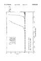
- FIG. 1is a schematic diagram of a conventional NAND Flash memory architecture of the prior art in which the biasing scheme of the present invention can be employed;
- FIGS. 2(a) and 2(b)are waveforms of the voltage applied to the control gates of the select gate devices and the unselected memory cell transistors and to the drain of the select gate during the Read operation, according to the present invention
- FIG. 3shows the measured source pull-up voltage as a function of sweeping the drain voltage positively with the control gate being set to +5.0 volts;
- FIG. 4is a test set-up for the method of eliminating hot-carrier disturb, according to the present invention.
- FIG. 5shows the read disturbance of the threshold voltage V T of the select gate in FIG. 4 as a function of the ramp-rate characteristic of the leading edge of the Read pulse applied to the drain.
- FIG. 1a schematic diagram of a conventional NAND Flash memory architecture 10 of the prior art in which the method of eliminating hot-carrier disturb of a floating gate device used as a select gate can be employed according to the present invention.
- the NAND Flash memory architecture 10includes an array sector 11 of Flash electrically erasable and programmable read-only memory (EEPROM) cells 12 (floating gate transistor devices) arranged in rows of word lines WL1, WL2, . . . WLn and columns of bit lines BL1, BL2, . . . BLn intersecting the rows of word lines so as to form the sector.
- EEPROMelectrically erasable and programmable read-only memory
- the array sector 11represents only one of a large number of identical sectors provided on a single integrated circuit memory chip.
- the NAND strings N1, N2, . . . Nn in the bit lines BL1, BL2, BL3, . . . BLn in the array sector 11has been shown.
- Each of the NAND stringsconsists of a plurality of the memory cells 12 (such as 16 cells) coupled between two select gate devices.
- each of the floating gate transistor devices 12 in each column of the bit lines BL1 . . . BLnis connected in series to the next floating gate transistor device 12 by joining the source 14 of one transistor device to the drain 16 of the next transistor device 12.
- Each of the control gates 18 of the transistor devices 12 in the same rowis connected to a corresponding one of the word lines WL1 . . . WLn.
- the select gate drain formed of floating gate transistors SGD1 . . . SGDnis coupled between one end of corresponding ones of the NAND strings and corresponding ones of the columns of bit lines BL1. . .BLn.
- the drain of the transistor SGD1is connected to a first power supply or potential V D and the source of the transistor SGD1 is connected to the drain of the array floating gate transistor 12 associated with the first word line WL1 in the NAND string N1.
- the drain of the transistor SGD2is connected to the supply potential V D and the source of the transistor SGD2 is connected to the drain of the array floating gate transistor 12 associated with the first word line in the NAND string N2.
- the drain of the transistor SGDnis connected to the supply potential V D and the source of the transistor SGDn is connected to the drain of the array floating gate transistor 12 associated with the first word line WL1 in the NAND string Nn.
- the gates of all of the select gate transistors SGD1 . . . SGDnare connected together and to a common line 19.
- a select gate source formed of floating gate transistor devices SGS1 . . . SGSnis coupled between the other end of corresponding ones of the NAND strings and a ground potential V S .
- the drain of the transistor SGS1is connected to the source of the array floating gate transistor 12 associated with the last word line WLn in the NAND string N1 and the source of the transistor SGS1 is connected to a second supply voltage or potential V S .
- the drain of the transistor SGS2is connected to the source of the array floating gate transistor 12 associated with the last word line WLn in the NAND string N2 and the source of the transistor SGS2 is connected to the second supply potential V S .
- the drain of the transistor SGSnis connected to the source of the array floating gate transistor 12 associated with the last word line in the NAND string Nn and the source of the transistor SGSn is connected to the second supply voltage V S .
- the gates of the floating gate transistors SGS1 . . . SGSnare connected together and to a common line 20. It will also be noted that the word lines WL1 . . . WLn are connected to receive a respective word line voltage V WL1 . . . V WLn . Further, the gates of the select gate drain transistors SGD1 . . . SGDn on the line 19 are connected to receive a select gate drain voltage V SG ,D. The gates of the select gate source transistors SGS1 . . . SGSn on the line 20 are connected to receive a select gate source voltage V SG ,S.
- a high drain voltage V Dis applied (e.g., for the NAND string N1) to the drain of the select gate drain transistor SGD1.
- the voltage V Dwill be approximately +3.5 volts for a 3 V Flash EEPROM array, and the voltage V S will be typically at zero volts.
- the select gate drain voltage V SG ,D applied to the gate of the select gate drain transistor SGD1is on the order of +4.5 V to +5.0 V.
- a problemarises when the drain voltage V D rises quickly so as to cause the drain-source voltage V ds across the select gate drain transistor to be greater than 1 volt. This will, in turn, create a high field to produce an accumulative soft unwanted programming of the select gate drain transistor SGD1.
- the inventorsconducted an investigation to explain the dependence of the source pull-up voltage V S1 of the select gate drain transistor SGD on the voltage applied to the drain during a Read operation.
- a constant current of 30 ⁇ Awas connected in series between the source and the ground potential in order to simulate a typical NAND read current.
- the source voltage V S1follows linearly the drain voltage V D so as to maintain the drain-source voltage V ds to be less than 0.3 volts.
- the problem of hot-carrier disturbwill not be an issue.
- the select gate drain SGDwill be in saturation causing hot-carrier programming. This operation suggests that no hot-carrier read disturb will occur if the select gate device is maintained in the linear region so as to minimize the drain-source voltage V ds . across its channel.
- FIG. 4 of the drawingsIn order to further demonstrate the source voltage V S1 dependence on the leading edge of the read pulse applied to the drain, an experimental or test set-up was constructed as shown in FIG. 4 of the drawings.
- a single gate transistor T1is connected in series with the floating gate transistor FGT used as a select gate drain device in order to simulate the NAND read operation.
- a gate voltage of V GT11.15 volts was applied to the gate of the single gate transistor T1 to set up a current of approximately 28 ⁇ A which resembles closely a typical read current.
- a fixed control gate voltage V FGT+5.0 V was applied to the control gate of the select gate drain device FGT.
- a read pulse, as shown on the right side of FIG. 4, having a pulse width of 10 ⁇ S and a maximum amplitude of +3.5 voltsis applied to the drain of the select gate drain transistor FGT. However, the value of the leading edge of the read pulse was varied.
- FIG. 5there is plotted the read disturb as measured by the threshold voltage V t shift, as a function of time for five different leading edge values with the applied bias conditions as defined in the inset. It can be observed that there was no threshold voltage V t shift when the value of the leading edge was longer than 250 nS and up to 1,000 nS. As the value of the leading edge is decreased, it will be noted that the threshold voltage V t shift occurs faster, indicative of hot-carrier programming.
- the read operation of the NAND memory architecture 10 of FIG. 1will now be explained with attention directed to FIGS. 2(a) and 2(b).
- the biasing scheme for eliminating hot-carrier disturb of the floating gate transistor used as a select gate drain in accordance with the principles of the present inventionis accomplished by controlling the gate voltage on the select gate device to overlap the read pulse applied to the drain and controlling simultaneously the leading edge of the read pulse so as to ramp up gradually.
- the improved biasing scheme of the present inventionwill maintain a drain-source voltage below 1.0 volts, thereby eliminating an accumulative soft unwanted programming of the select gate drain device.
- FIG. 2(a)there is illustrated the waveform of the gate pulse voltages V SG ,D V SG ,S and V WL1 . . . V WLn applied to the respective control gates of the select gate drain transistors SGD1 . . . SGDn, the select gate source transistors SGS1 . . . SGSn, and the unselected array floating gate transistors 12 in the NAND memory architecture 10 during the Read operation utilizing the biasing scheme of the present invention. It should be noted that zero volts is applied to the control gates of the selected array floating gate transistors 12 which are to be read.
- FIG. 2(b)there is depicted the waveform of the read pulse voltage V D applied to the drain of the select gate drain transistors SGD1 . . . SGDn during this Read operation.
- the select gate drain devices and the select gate source devices formed by the floating gate transistors illustrated in FIG. 1are replaced with single gate transistors. It should be understood by those skilled in the art that the method of eliminating hot-carrier disturb of the present invention described above is equally applicable to this alternate embodiment. Thus, the details of the biasing scheme of the present invention will not be repeated.
- the present inventionprovides an improved method for eliminating hot-carrier disturb of a floating gate device used as a select gate during a read operation for NAND memory architecture.
- the biasing scheme of the present inventionminimizes the drain-source voltage across the channel of the select gate device so as to maintain its operation in the linear region, thereby eliminating hot-carrier read disturb. This is achieved by applying a first positive pulse voltage having a ramp-rate characteristic on its leading edge to the drain of the select gate device during the read operation and simultaneously applying a second positive pulse voltage to the control gate of the select gate device so as to overlap the first positive pulse voltage.
Landscapes
- Non-Volatile Memory (AREA)
- Semiconductor Memories (AREA)
Abstract
Description
Claims (20)
Priority Applications (1)
| Application Number | Priority Date | Filing Date | Title |
|---|---|---|---|
| US08/810,170US5815438A (en) | 1997-02-28 | 1997-02-28 | Optimized biasing scheme for NAND read and hot-carrier write operations |
Applications Claiming Priority (1)
| Application Number | Priority Date | Filing Date | Title |
|---|---|---|---|
| US08/810,170US5815438A (en) | 1997-02-28 | 1997-02-28 | Optimized biasing scheme for NAND read and hot-carrier write operations |
Publications (1)
| Publication Number | Publication Date |
|---|---|
| US5815438Atrue US5815438A (en) | 1998-09-29 |
Family
ID=25203189
Family Applications (1)
| Application Number | Title | Priority Date | Filing Date |
|---|---|---|---|
| US08/810,170Expired - LifetimeUS5815438A (en) | 1997-02-28 | 1997-02-28 | Optimized biasing scheme for NAND read and hot-carrier write operations |
Country Status (1)
| Country | Link |
|---|---|
| US (1) | US5815438A (en) |
Cited By (13)
| Publication number | Priority date | Publication date | Assignee | Title |
|---|---|---|---|---|
| US5973962A (en)* | 1997-12-29 | 1999-10-26 | Samsung Electronics Co., Ltd. | Method of programming non-volatile memory devices having a NAND type cell array |
| US5991202A (en)* | 1998-09-24 | 1999-11-23 | Advanced Micro Devices, Inc. | Method for reducing program disturb during self-boosting in a NAND flash memory |
| US6023426A (en)* | 1998-03-09 | 2000-02-08 | Eon Silicon Devices, Inc. | Method of achieving narrow VT distribution after erase in flash EEPROM |
| US20050056869A1 (en)* | 2003-08-04 | 2005-03-17 | Kabushiki Kaisha Toshiba | Nonvolatile semiconductor memory cell matrix, a mehtod for operating the same, monolithic integrated circuits and systems |
| US20050180186A1 (en)* | 2004-02-13 | 2005-08-18 | Lutze Jeffrey W. | Shield plate for limiting cross coupling between floating gates |
| US20060239079A1 (en)* | 2002-01-18 | 2006-10-26 | Nima Mokhlesi | Noise Reduction Technique for Transistors and Small Devices Utilizing an Episodic Agitation |
| US20100246263A1 (en)* | 2007-02-22 | 2010-09-30 | Hynix Semiconductor Inc. | Non-volatile Memory Device |
| US8611158B2 (en)* | 2011-08-30 | 2013-12-17 | Elpida Memory, Inc. | Systems and methods for erasing charge-trap flash memory |
| DE112004003023B4 (en)* | 2004-11-30 | 2017-11-02 | Spansion Llc (N.D.Ges.D. Staates Delaware) | Semiconductor device and method for controlling the semiconductor device |
| US10115464B1 (en) | 2017-07-27 | 2018-10-30 | Sandisk Technologies Llc | Electric field to reduce select gate threshold voltage shift |
| US10146451B2 (en) | 2015-12-10 | 2018-12-04 | SK Hynix Inc. | Reducing read disturb in data storage |
| DE112004003160B3 (en) | 2004-11-30 | 2022-07-28 | Spansion Llc (N.D.Ges.D. Staates Delaware) | Semiconductor device and method for controlling the semiconductor device |
| CN114882929A (en)* | 2021-02-05 | 2022-08-09 | 旺宏电子股份有限公司 | Operation method of storage device |
Citations (3)
| Publication number | Priority date | Publication date | Assignee | Title |
|---|---|---|---|---|
| US5589699A (en)* | 1993-12-27 | 1996-12-31 | Kabushiki Kaisha Toshiba | Electrically erasable programmable non-volatile semiconductor memory device having select gates and small number of contact holes |
| US5591999A (en)* | 1993-06-08 | 1997-01-07 | Kabushiki Kaisha Toshiba | Electrically erasable programmable read only memory device with an improved memory cell pattern layout |
| US5694356A (en)* | 1994-11-02 | 1997-12-02 | Invoice Technology, Inc. | High resolution analog storage EPROM and flash EPROM |
- 1997
- 1997-02-28USUS08/810,170patent/US5815438A/ennot_activeExpired - Lifetime
Patent Citations (3)
| Publication number | Priority date | Publication date | Assignee | Title |
|---|---|---|---|---|
| US5591999A (en)* | 1993-06-08 | 1997-01-07 | Kabushiki Kaisha Toshiba | Electrically erasable programmable read only memory device with an improved memory cell pattern layout |
| US5589699A (en)* | 1993-12-27 | 1996-12-31 | Kabushiki Kaisha Toshiba | Electrically erasable programmable non-volatile semiconductor memory device having select gates and small number of contact holes |
| US5694356A (en)* | 1994-11-02 | 1997-12-02 | Invoice Technology, Inc. | High resolution analog storage EPROM and flash EPROM |
Cited By (23)
| Publication number | Priority date | Publication date | Assignee | Title |
|---|---|---|---|---|
| US5973962A (en)* | 1997-12-29 | 1999-10-26 | Samsung Electronics Co., Ltd. | Method of programming non-volatile memory devices having a NAND type cell array |
| US6023426A (en)* | 1998-03-09 | 2000-02-08 | Eon Silicon Devices, Inc. | Method of achieving narrow VT distribution after erase in flash EEPROM |
| US5991202A (en)* | 1998-09-24 | 1999-11-23 | Advanced Micro Devices, Inc. | Method for reducing program disturb during self-boosting in a NAND flash memory |
| US20060239079A1 (en)* | 2002-01-18 | 2006-10-26 | Nima Mokhlesi | Noise Reduction Technique for Transistors and Small Devices Utilizing an Episodic Agitation |
| US7403421B2 (en)* | 2002-01-18 | 2008-07-22 | Sandisk Corporation | Noise reduction technique for transistors and small devices utilizing an episodic agitation |
| US7649777B2 (en)* | 2003-08-04 | 2010-01-19 | Kabushiki Kaisha Toshiba | Nonvolatile semiconductor memory cell matrix with divided write/erase, a method for operating the same, monolithic integrated circuits and systems |
| US20050056869A1 (en)* | 2003-08-04 | 2005-03-17 | Kabushiki Kaisha Toshiba | Nonvolatile semiconductor memory cell matrix, a mehtod for operating the same, monolithic integrated circuits and systems |
| US20080116502A1 (en)* | 2004-02-13 | 2008-05-22 | Lutze Jeffrey W | Non-volatile memory with epitaxial regions for limiting cross coupling between floating gates |
| US20080124865A1 (en)* | 2004-02-13 | 2008-05-29 | Lutze Jeffrey W | Method for forming non-volatile memory with shield plate for limiting cross coupling between floating gates |
| US20050180186A1 (en)* | 2004-02-13 | 2005-08-18 | Lutze Jeffrey W. | Shield plate for limiting cross coupling between floating gates |
| US7807533B2 (en) | 2004-02-13 | 2010-10-05 | Sandisk Corporation | Method for forming non-volatile memory with shield plate for limiting cross coupling between floating gates |
| US7834386B2 (en) | 2004-02-13 | 2010-11-16 | Sandisk Corporation | Non-volatile memory with epitaxial regions for limiting cross coupling between floating gates |
| US7355237B2 (en)* | 2004-02-13 | 2008-04-08 | Sandisk Corporation | Shield plate for limiting cross coupling between floating gates |
| DE112004003160B3 (en) | 2004-11-30 | 2022-07-28 | Spansion Llc (N.D.Ges.D. Staates Delaware) | Semiconductor device and method for controlling the semiconductor device |
| DE112004003023B4 (en)* | 2004-11-30 | 2017-11-02 | Spansion Llc (N.D.Ges.D. Staates Delaware) | Semiconductor device and method for controlling the semiconductor device |
| US20100246263A1 (en)* | 2007-02-22 | 2010-09-30 | Hynix Semiconductor Inc. | Non-volatile Memory Device |
| US8611158B2 (en)* | 2011-08-30 | 2013-12-17 | Elpida Memory, Inc. | Systems and methods for erasing charge-trap flash memory |
| US10146451B2 (en) | 2015-12-10 | 2018-12-04 | SK Hynix Inc. | Reducing read disturb in data storage |
| WO2019022811A1 (en)* | 2017-07-27 | 2019-01-31 | Sandisk Technologies Llc | Electric field to reduce select gate threshold voltage shift |
| CN110800059A (en)* | 2017-07-27 | 2020-02-14 | 桑迪士克科技有限责任公司 | Electric field to reduce select gate threshold voltage shift |
| US10115464B1 (en) | 2017-07-27 | 2018-10-30 | Sandisk Technologies Llc | Electric field to reduce select gate threshold voltage shift |
| CN110800059B (en)* | 2017-07-27 | 2023-08-25 | 桑迪士克科技有限责任公司 | Nonvolatile memory device and method of operating the same |
| CN114882929A (en)* | 2021-02-05 | 2022-08-09 | 旺宏电子股份有限公司 | Operation method of storage device |
Similar Documents
| Publication | Publication Date | Title |
|---|---|---|
| US5838617A (en) | Method for changing electrically programmable read-only memory devices | |
| US5696717A (en) | Nonvolatile integrated circuit memory devices having adjustable erase/program threshold voltage verification capability | |
| US6853598B2 (en) | Non-volatile memory with test rows for disturb detection | |
| US5553020A (en) | Structure and method for low current programming of flash EEPROMs | |
| US7212435B2 (en) | Minimizing adjacent wordline disturb in a memory device | |
| KR100331563B1 (en) | NAND-type flash memory device and method for operating the same | |
| US4434478A (en) | Programming floating gate devices | |
| JP3653186B2 (en) | Nonvolatile memory device programming method | |
| US5508959A (en) | Programming method for the selective healing of over-erased cells on a flash erasable programmable read-only memory device | |
| KR100761091B1 (en) | Gate ramping technology allows soft programming to narrow the NT distribution | |
| US5973962A (en) | Method of programming non-volatile memory devices having a NAND type cell array | |
| US6205059B1 (en) | Method for erasing flash electrically erasable programmable read-only memory (EEPROM) | |
| JP3652453B2 (en) | Semiconductor memory device | |
| US5790456A (en) | Multiple bits-per-cell flash EEPROM memory cells with wide program and erase Vt window | |
| US5323351A (en) | Method and apparatus for programming electrical erasable programmable read-only memory arrays | |
| US6240016B1 (en) | Method to reduce read gate disturb for flash EEPROM application | |
| US6438037B1 (en) | Threshold voltage compacting for non-volatile semiconductor memory designs | |
| US5521867A (en) | Adjustable threshold voltage conversion circuit | |
| US5815438A (en) | Optimized biasing scheme for NAND read and hot-carrier write operations | |
| US5805499A (en) | Channel hot-carrier page write for NAND applications | |
| KR940008204B1 (en) | Over-erase prevention apparatus and method of nand type fiash memroy | |
| US5619454A (en) | Programming method for healing over-erased cells for a flash memory device | |
| US6285588B1 (en) | Erase scheme to tighten the threshold voltage distribution of EEPROM flash memory cells | |
| US5633823A (en) | Method of narrowing flash memory device threshold voltage distribution | |
| US6178117B1 (en) | Background correction for charge gain and loss |
Legal Events
| Date | Code | Title | Description |
|---|---|---|---|
| AS | Assignment | Owner name:ADVANCED MICRO DEVICES, INC., CALIFORNIA Free format text:ASSIGNMENT OF ASSIGNORS INTEREST;ASSIGNORS:HADDAD, SAMEER S.;CHEN, PAU-LING;REEL/FRAME:008450/0406 Effective date:19970217 | |
| FEPP | Fee payment procedure | Free format text:PAYOR NUMBER ASSIGNED (ORIGINAL EVENT CODE: ASPN); ENTITY STATUS OF PATENT OWNER: LARGE ENTITY | |
| STCF | Information on status: patent grant | Free format text:PATENTED CASE | |
| CC | Certificate of correction | ||
| FPAY | Fee payment | Year of fee payment:4 | |
| FPAY | Fee payment | Year of fee payment:8 | |
| AS | Assignment | Owner name:SPANSION INC., CALIFORNIA Free format text:ASSIGNMENT OF ASSIGNORS INTEREST;ASSIGNOR:ADVANCED MICRO DEVICES, INC.;REEL/FRAME:019028/0617 Effective date:20070131 | |
| AS | Assignment | Owner name:SPANSION LLC, CALIFORNIA Free format text:ASSIGNMENT OF ASSIGNORS INTEREST;ASSIGNOR:SPANSION INC.;REEL/FRAME:019069/0013 Effective date:20070131 | |
| FPAY | Fee payment | Year of fee payment:12 | |
| AS | Assignment | Owner name:BARCLAYS BANK PLC,NEW YORK Free format text:SECURITY AGREEMENT;ASSIGNORS:SPANSION LLC;SPANSION INC.;SPANSION TECHNOLOGY INC.;AND OTHERS;REEL/FRAME:024522/0338 Effective date:20100510 Owner name:BARCLAYS BANK PLC, NEW YORK Free format text:SECURITY AGREEMENT;ASSIGNORS:SPANSION LLC;SPANSION INC.;SPANSION TECHNOLOGY INC.;AND OTHERS;REEL/FRAME:024522/0338 Effective date:20100510 | |
| AS | Assignment | Owner name:SPANSION TECHNOLOGY LLC, CALIFORNIA Free format text:RELEASE OF LIEN ON PATENT;ASSIGNOR:BARCLAYS BANK PLC;REEL/FRAME:030945/0505 Effective date:20130805 Owner name:SPANSION TECHNOLOGY INC., CALIFORNIA Free format text:RELEASE OF LIEN ON PATENT;ASSIGNOR:BARCLAYS BANK PLC;REEL/FRAME:030945/0505 Effective date:20130805 Owner name:SPANSION INC., CALIFORNIA Free format text:RELEASE OF LIEN ON PATENT;ASSIGNOR:BARCLAYS BANK PLC;REEL/FRAME:030945/0505 Effective date:20130805 Owner name:SPANSION LLC, CALIFORNIA Free format text:RELEASE OF LIEN ON PATENT;ASSIGNOR:BARCLAYS BANK PLC;REEL/FRAME:030945/0505 Effective date:20130805 | |
| AS | Assignment | Owner name:VALLEY DEVICE MANAGEMENT, DELAWARE Free format text:ASSIGNMENT OF ASSIGNORS INTEREST;ASSIGNOR:SPANSION LLC;REEL/FRAME:035961/0484 Effective date:20130731 |