US5815310A - High numerical aperture ring field optical reduction system - Google Patents
High numerical aperture ring field optical reduction systemDownload PDFInfo
- Publication number
- US5815310A US5815310AUS08/571,081US57108195AUS5815310AUS 5815310 AUS5815310 AUS 5815310AUS 57108195 AUS57108195 AUS 57108195AUS 5815310 AUS5815310 AUS 5815310A
- Authority
- US
- United States
- Prior art keywords
- mirror
- concave mirror
- refl
- concave
- reduction system
- Prior art date
- Legal status (The legal status is an assumption and is not a legal conclusion. Google has not performed a legal analysis and makes no representation as to the accuracy of the status listed.)
- Expired - Lifetime
Links
Images

Classifications
- G—PHYSICS
- G02—OPTICS
- G02B—OPTICAL ELEMENTS, SYSTEMS OR APPARATUS
- G02B27/00—Optical systems or apparatus not provided for by any of the groups G02B1/00 - G02B26/00, G02B30/00
- G02B27/18—Optical systems or apparatus not provided for by any of the groups G02B1/00 - G02B26/00, G02B30/00 for optical projection, e.g. combination of mirror and condenser and objective
- G—PHYSICS
- G03—PHOTOGRAPHY; CINEMATOGRAPHY; ANALOGOUS TECHNIQUES USING WAVES OTHER THAN OPTICAL WAVES; ELECTROGRAPHY; HOLOGRAPHY
- G03F—PHOTOMECHANICAL PRODUCTION OF TEXTURED OR PATTERNED SURFACES, e.g. FOR PRINTING, FOR PROCESSING OF SEMICONDUCTOR DEVICES; MATERIALS THEREFOR; ORIGINALS THEREFOR; APPARATUS SPECIALLY ADAPTED THEREFOR
- G03F7/00—Photomechanical, e.g. photolithographic, production of textured or patterned surfaces, e.g. printing surfaces; Materials therefor, e.g. comprising photoresists; Apparatus specially adapted therefor
- G03F7/70—Microphotolithographic exposure; Apparatus therefor
- G03F7/70216—Mask projection systems
- G03F7/70225—Optical aspects of catadioptric systems, i.e. comprising reflective and refractive elements
- G—PHYSICS
- G02—OPTICS
- G02B—OPTICAL ELEMENTS, SYSTEMS OR APPARATUS
- G02B17/00—Systems with reflecting surfaces, with or without refracting elements
- G02B17/02—Catoptric systems, e.g. image erecting and reversing system
- G02B17/06—Catoptric systems, e.g. image erecting and reversing system using mirrors only, i.e. having only one curved mirror
- G02B17/0647—Catoptric systems, e.g. image erecting and reversing system using mirrors only, i.e. having only one curved mirror using more than three curved mirrors
- G02B17/0657—Catoptric systems, e.g. image erecting and reversing system using mirrors only, i.e. having only one curved mirror using more than three curved mirrors off-axis or unobscured systems in which all of the mirrors share a common axis of rotational symmetry
- G—PHYSICS
- G03—PHOTOGRAPHY; CINEMATOGRAPHY; ANALOGOUS TECHNIQUES USING WAVES OTHER THAN OPTICAL WAVES; ELECTROGRAPHY; HOLOGRAPHY
- G03F—PHOTOMECHANICAL PRODUCTION OF TEXTURED OR PATTERNED SURFACES, e.g. FOR PRINTING, FOR PROCESSING OF SEMICONDUCTOR DEVICES; MATERIALS THEREFOR; ORIGINALS THEREFOR; APPARATUS SPECIALLY ADAPTED THEREFOR
- G03F7/00—Photomechanical, e.g. photolithographic, production of textured or patterned surfaces, e.g. printing surfaces; Materials therefor, e.g. comprising photoresists; Apparatus specially adapted therefor
- G03F7/70—Microphotolithographic exposure; Apparatus therefor
- G03F7/70216—Mask projection systems
- G03F7/70233—Optical aspects of catoptric systems, i.e. comprising only reflective elements, e.g. extreme ultraviolet [EUV] projection systems
- G—PHYSICS
- G03—PHOTOGRAPHY; CINEMATOGRAPHY; ANALOGOUS TECHNIQUES USING WAVES OTHER THAN OPTICAL WAVES; ELECTROGRAPHY; HOLOGRAPHY
- G03F—PHOTOMECHANICAL PRODUCTION OF TEXTURED OR PATTERNED SURFACES, e.g. FOR PRINTING, FOR PROCESSING OF SEMICONDUCTOR DEVICES; MATERIALS THEREFOR; ORIGINALS THEREFOR; APPARATUS SPECIALLY ADAPTED THEREFOR
- G03F7/00—Photomechanical, e.g. photolithographic, production of textured or patterned surfaces, e.g. printing surfaces; Materials therefor, e.g. comprising photoresists; Apparatus specially adapted therefor
- G03F7/70—Microphotolithographic exposure; Apparatus therefor
- G03F7/70216—Mask projection systems
- G03F7/70275—Multiple projection paths, e.g. array of projection systems, microlens projection systems or tandem projection systems
Definitions
- This inventionrelates generally to projection lithography, and more particularly to a catoptric and catadioptric optical system for use with short wavelengths in the near and extreme ultraviolet or soft X-ray region.
- PhotolithographyIn the manufacture of semiconductor devices, photolithography is often used. Projection optics are used to image a mask or reticle onto a wafer. Optical systems using refractive elements have achieved resolutions approaching 0.25 micrometers operating with illumination sources having wavelengths of 248 or 193 nanometers. As the element or feature size of semiconductor devices become smaller, the need for optical projection systems capable of providing a resolution less than 0.25 micrometers are needed. In order to decrease the feature size which the optical projection systems used in photolithography can resolve, shorter wavelengths of electromagnetic radiation must be used to project the image of a reticle or mask onto a photosensitive substrate, such as a semiconductor wafer.
- optical projection systemsWhile there are several optical projection systems that operate within this wavelength region, they are limited to a relatively low numerical aperture of less than 0.1 at the image or wafer. Increasing the numerical aperture of these designs will result in unacceptably large residual aberrations and obscuration of the light beams by the edges of the mirrors. While these projection optical systems perform adequately for their intended purpose, there is a need for optical projection systems having a higher numerical aperture for use at wavelengths in the extreme ultraviolet or soft x-ray wavelengths, or for resolutions substantially less than 0.1 micrometers or microns.
- the present inventioncomprises three mirror pairs.
- the first mirror pairincludes a positive power mirror imaging an entrance pupil onto a second mirror of the first mirror pair providing an accessible, real aperture stop.
- a second mirror pairreceives electromagnetic radiation from the first mirror pair and includes a positive power mirror relaying the aperture stop to a second real pupil and forming an intermediate image.
- a third mirror pairreceives electromagnetic radiation from the second mirror pair, and includes a positive power mirror relaying the second real pupil to an exit pupil at infinity and imaging the intermediate image to a real final image.
- a six mirror reduction system of relatively high numerical apertureis thereby obtained that provides a reduced image of an object, such as a reticle or mask, onto a photosensitive substrate, such as a semiconductor wafer.
- the second mirror pairacts as a field mirror element providing a relatively high numerical aperture with good or acceptable image quality. All six mirrors may be aspheric to obtain the smallest possible residual aberrations.
- an aperture stopis accessible.
- FIG. 1is a schematic illustration of one embodiment of the present invention.
- FIG. 2is a schematic illustration of a second embodiment of the present invention.
- FIG. 3is a schematic illustration of a third embodiment of the present invention.
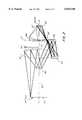
- FIG. 1schematically illustrates a first embodiment of the present invention.
- the light from a reticle or mask 10is collected by concave mirror M1.
- Dashed line 12represents the extended curvature of mirror M1.
- Mirror M1reflects electromagnetic radiation to concave mirror M2.
- An aperture stop 14is positioned at or near mirror M2.
- An entrance pupilis positioned a finite distance from the reticle or mask 10 and imaged at mirror M2 by mirror M1.
- Electromagnetic radiationis reflected from mirror M2 to concave mirror M3.
- Dashed line 16illustrates the extended curvature of concave mirror M3.
- Electromagnetic radiation from mirror M3is received and reflected by concave mirror M4.
- Dashed line 18illustrates the extended curvature of concave mirror M4.
- Electromagnetic radiationis reflected from mirror M4 and received by convex mirror M5.
- Dashed line 20illustrates the extended curvature of convex mirror M5.
- Electromagnetic radiationis reflected from mirror M5 and received by concave mirror M6, and reflected by concave mirror M6 to an image location at a wafer 22. All of the mirrors M1-M6 are substantially rotationally symmetric about the optical axis OA.
- An intermediate image 24is formed between the mirrors M4 and M3 or at an off-axis location between the first mirror pair, M1 and M2, and the third mirror pair, M5 and M6. This intermediate image is re-imaged at the wafer 22 by mirrors M4, M5, and M6.
- the first mirror pair, M1 and M2reflects electromagnetic radiation to a second mirror pair, M3 and M4.
- the second mirror pair, M3 and M4functions as a field mirror element and takes the chief ray leaving mirror M2 diverging away from the optical axis OA, and converts it to a chief ray converging toward the optical axis OA for acceptance by a third mirror pair, M5 and M6.
- a field mirror elementmay be a mirror pair that converts a chief ray diverging away from the optical axis OA to a chief ray converging towards the optical axis OA.
- the residual aberrationsare small enough to permit use at a wavelength of approximately 13 nanometers.
- the numerical aperture in the image space near the wafer 22 in this first embodimentis approximately 0.25. This provides a working resolution of 0.03 micrometers or microns.
- An annular image field having a radius between 29 and 31 millimeters from the optical axis OAhas aberrations, including distortions small enough for use in a step and scan photolithography system with a scanned field size of 30 millimeters in the cross scan direction. In this first embodiment, a four to one reduction is obtained.
- Mirrors M1-M6may be spherical or aspheric and fabricated by any conventional means, including the placement of coatings thereon such as disclosed in U.S. Pat. No.
- positive radiusindicates the center of curvature is to the right
- negative radiusindicates the center of curvature is to the left
- dimensionsare given in millimeters
- thicknessis axial distance to next surface
- image diameter shown aboveis a paraxial value and is not a ray traced value.
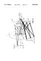
- FIG. 2illustrates a second embodiment of the present invention.
- the entrance pupilis at infinity, resulting in the system being telecentric at the reticle 10.
- Electromagnetic radiation from the reticle 10is collected by concave mirror M1' and reflected to convex mirror M2'.
- Dashed line 12'represents the extended curvature of mirror M1'.
- Mirrors M1' and M2'form a first mirror pair.
- Electromagnetic radiation reflected from convex mirror M2'is collected by concave mirror M3'.
- Dashed line 16'represents the extended curvature of mirror M3'.
- Electromagnetic radiationis reflected from mirror M3' to concave mirror M4'.
- Dashed line 18'represents the extended curvature of mirror M4'.
- Mirrors M3' and M4'form a second mirror pair acting as a field mirror element. Electromagnetic radiation is reflected from mirror M4' and is collected by convex mirror M5'. Dashed line 20' represents the extended curvature of mirror M5'. Electromagnetic radiation is reflected from mirror M5' and collected by mirror M6'. Mirrors M5' and M6' form a third mirror pair. The electromagnetic radiation reflected from the concave mirror M6' is imaged at a wafer 22. All of the mirrors M1'-M6' are rotationally symmetrical about the optical axis OA.
- the field mirror element mirror pair M4' and M3'form an intermediate image plane 24' after mirror M4' and close to mirror M6' or at an off-axis location between the mirrors of the third mirror pair M5' and M6'.
- Thisis advantageous at high numerical apertures to minimize the electromagnetic radiation beam size that has to clear the edge of mirror M6'.
- the third mirror pair, mirrors M5' and M6're-image the image at the intermediate image plane 24' to a final image at the wafer 22.
- the image spaceis telecentric, that is the exit pupil is at infinity.
- This second embodimenthas a four to one reduction ratio, and the numerical aperture into the image space near the wafer 22 is 0.55.
- the optical projection systemmay be used at wavelengths of approximately 193 nanometers. This allowing a working resolution of 0.25 microns or micrometers.
- An annular field formed between a radius of 29.5 and 30.5 millimeters from the optical axis OA at the wafer 22is sufficient for use in a step and scan lithography system with a field size of 30 millimeters in the cross-scan direction.
- positive radiusindicates the center of curvature is to the right
- negative radiusindicates the center of curvature is to the left
- dimensionsare given in millimeters
- thicknessis axial distance to next surface
- image diameter shown aboveis a paraxial value and is not a ray traced value.
- FIG. 3illustrates a third embodiment of the present invention.
- This third embodimentillustrates a catadioptric system.
- Electromagnetic radiation from the reticle 10is refracted by a first lens element R1.
- the electromagnetic radiationis then collected by concave mirror M1" and reflected, to a second lens element R2.
- Lens element R2is near or adjacent convex mirror M2".
- Mirrors M1" and M2"form a first mirror pair.
- Dashed line 12"represents the extended curvature of mirror M1".
- Electromagnetic radiationis reflected from mirror M2" and collected by mirror M3".
- Dashed line 16"represents the curvature of concave mirror M3".
- Electromagnetic radiationis reflected from mirror M3" and collected by concave mirror M4".
- Dashed line 18"represents the curvature of mirror M4".
- Mirrors M3" and M4"form a second mirror pair. Electromagnetic radiation reflected from mirror M4" is collected by convex mirror M5". Electromagnetic radiation reflected from mirror M5" is collected by concave mirror M6". Mirrors M5" and M6" form a third mirror pair. Electromagnetic radiation reflected from mirror M6" is directed to a lens element R3 and is then imaged at an image plane at wafer 22. The second mirror pair, mirrors M3" and M4", form a field mirror element providing an intermediate image plane 24" between mirrors M6" and M3". The third mirror pair M5" and M6" re-image intermediate image plane 24" at the wafer 22.
- All of the mirrors M1"-M6" and the refractive lens elements R1-R3are rotationally symmetrical about the optical axis OA.
- the lens elements R1-R3are refracting elements that reduce residual aberrations allowing operation at a higher numerical aperture in the image space near the wafer 22.
- the numerical aperture at the image space near the wafer 22is 0.6.
- An annular field having a radius between 29 and 31 millimeters from the optical axis OAis formed that may comfortably resolve 0.225 micron features using electromagnetic radiation at a wavelength of 193 nanometers. In this third embodiment 0.18 micron feature sizes may be achievable with the appropriate reticles, illumination conditions, and photo resist.
- first lens element R1may also serve as a sealing window if desired. This is desirable when the system is used in a purged environment.
- Lens element R1may additionally be moved axially along the optical axis OA to make fine adjustments to system magnification. While the mirror M1" could be used for fine adjustments to magnification, mirror M1" is much more sensitive to alignment errors during axial movement.
- Lens element R3may also be used as a sealing window. Additionally, lens element R3 may act as a substrate on which mirror M5" may be formed.
- the lens element R3may have an aspheric second surface primarily to reduce residual distortion errors. This, the second surface of lens element R3, allows a wider annular field width to be used.
- Lens element R2is primarily used to correct the chromatic variation of focus introduced by refractive lens elements R1 and R3. Chromatic variation of magnification is corrected by balancing the contributions of chromatic variations of magnification from lens elements R1 and R3. Chromatic correction is good enough in this embodiment to allow the use of an unnarrowed excimer laser source operating at 193 or 248 nanometers, or even a filtered mercury lamp operating at 248 nanometers.
- the optical projection system of this third embodimentis designed to operate at a four to one reduction ratio.
- positive radiusindicates the center of curvature is to the right
- negative radiusindicates the center of curvature is to the left
- dimensionsare given in millimeters
- thicknessis axial distance to next surface
- image diameter shown aboveis a paraxial value and is not a ray traced value.
- the present inventionby using three mirror pairs, with the second mirror pair being a field mirror element, greatly increases the numerical aperture possible in an optical projection reduction system for use with electromagnetic radiation at wavelengths below approximately 200 nanometers. This greatly increases the field size as well as maintaining necessary resolution, permitting practical application for use in the manufacture of semiconductor devices having features smaller than 0.25 microns.
Landscapes
- Physics & Mathematics (AREA)
- General Physics & Mathematics (AREA)
- Optics & Photonics (AREA)
- Lenses (AREA)
- Exposure And Positioning Against Photoresist Photosensitive Materials (AREA)
- Exposure Of Semiconductors, Excluding Electron Or Ion Beam Exposure (AREA)
Abstract
Description
TABLE 1 ______________________________________ Radius of Element Curvature Aperture Diameter Number Front Back Thickness Front Back Glass ______________________________________ object Infinity 571.0624 236.9146 192.0526 1 A(1) -192.0526 233.4582 Refl Aperture Stop 46.3098 0.0000 2 A(2) 0.0000 45.7172 Refl 45.2145 432.1152 3 A(3) -490.5496 334.0156 Refl 4 A(4) 490.5496 503.2223 Refl 240.0123 -62.8918 261.2488 320.6990 5 A(5) -320.6990 86.6738 Refl 6 A(6) 320.6990 227.7070 Refl 72.1652 Image Distance = 22.3092 Image INF 62.0000 ______________________________________
TABLE 1A __________________________________________________________________________Aspheric Curv K A B C D __________________________________________________________________________A(1) -0.00204178 0.000000 6.26871E - 10 -1.09535E - 15 1.29067E - 20 8.68980E - 26 A(2) -0.00248086 0.000000 1.05970E - 08 4.81436E - 13 -1.10750E - 15 7.52743E - 19 A(3) -0.00048280 0.000000 2.18257E - 11 2.87915E - 15 6.04832E - 20 3.68423E - 25 A(4) 0.00101457 0.000000 3.42885E - 11 -4.85608E - 16 -3.57675E - 22 1.81445E - 26 A(5) 0.00355137 0.000000 1.77414E - 08 1.15815E - 12 7.13212E - 17 -4.35391E - 21 A(6) 0.00258825 0.000000 1.36198E - 10 1.22849E - 15 8.27928E - 21 1.16903E - 25 __________________________________________________________________________
TABLE 2 ______________________________________ Radius of Element Curvature Aperture Diameter Number Front Back Thickness Front Back Glass ______________________________________ object Infinity 407.8161 357.5906 264.5379 1 A(1) -264.5379 419.5247 Refl Aperture Stop 77.5026 0.0000 2 A(2) 0.0000 74.9379 Refl 77.3224 390.2371 3 A(3) -260.0000 467.2174 Refl 4 A(4) 260.0000 527.2466 Refl 240.4502 -5.6992 206.6446 186.2863 5 A(5) -186.2863 92.0895 Refl 6 A(6) 186.2863 272.0463 Refl 82.3061 Image Distance = 20.0000 Image INF 60.9996 ______________________________________
TABLE 2A __________________________________________________________________________ K A B C D Aspheric Curv E F G H J __________________________________________________________________________A(1) -0.00184131 0.000000 2.24506E - 12 -1.06529E - 15 1.40153E - 20 -1.45525E - 26 0.00000E + 00 0.00000E + 00 0.00000E + 00 0.00000E + 00 0.00000E + 00 A(2) -0.00344767 0.000000 2.70239E - 08 6.29102E - 12 1.39941E - 15 -1.11823E - 19 3.43046E - 23 0.00000E + 00 0.00000E + 00 0.00000E + 00 0.00000E + 00 A(3) -0.00073996 0.000000 3.47651E - 10 1.86467E - 16 -3.27086E - 20 1.15234E - 25 0.00000E + 00 0.00000E + 00 0.00000E + 00 0.00000E + 00 0.00000E + 00 A(4) 0.00145483 0.000000 -6.10242E - 11 7.82453E - 16 -8.98158E - 21 -4.15911E - 26 0.00000E + 00 0.00000E + 00 0.00000E + 00 0.00000E + 00 0.00000E + 00 A(5) 0.00444460 0.000000 1.67615E - 07 1.75232E - 11 8.40253E - 16 8.38291E - 20 6.03283E - 23 0.00000E + 00 0.00000E + 00 0.00000E + 00 0.00000E + 00 A(6) 0.00442274 0.000000 5.24492E - 10 8.43072E - 15 4.12933E - 19 -9.76520E - 24 5.15810E - 28 0.00000E + 00 0.00000E + 00 0.00000E + 00 0.00000E + 00 __________________________________________________________________________
TABLE 3 __________________________________________________________________________Element Radius of Curvature Aperature Diameter Number Front Back Thickness Front Back Glass __________________________________________________________________________Object INF 363.7117 1 528.5985 CX 560.6353 CC 30.0000 369.2458 367.0565 `silica` 20.0000 364.0844 229.7508 2 A(1) -209.7508 414.3396 Refl 3 -83.4955 CX -75.5672 CC -15.0000 97.0160 79.4269 `silica` -11.6150 Aperture Stop 72.1226 4 A(2) 11.6150 72.1226 Refl 5 -75.5672 CC -83.4955 CX 15.0000 77.0143 93.4487 `silica` 407.8622 6 A(3) -635.1022 691.6152 Refl 7 A(4) 635.1022 1006.3416 Refl 131.7841 -62.2903 177.7085 134.7903 8 A(5) -134.7903 89.6331 Refl 9 A(6) 134.7903 223.8931 Refl 10 A(7) A(8) 17.5000 88.9023 73.3478 `silica` Image Distance = 10.0000 IMAGE INF 62.0953 __________________________________________________________________________
TABLE 3A __________________________________________________________________________ K A B C D Aspheric Curv E F G H J __________________________________________________________________________A(1) -0.00204511 0.000000 2.33031E - 10 -2.45108E - 16 1.19279E - 20 7.03022E - 26 0.00000E + 00 0.00000E + 00 0.00000E + 00 0.00000E + 00 0.00000E + 00 A(2) -0.00552141 0.000000 -3.13911E - 09 5.79100E - 12 -7.42414E - 16 1.18359E - 18 -2.35686E - 22 0.00000E + 00 0.00000E + 00 0.00000E + 00 0.00000E + 00 A(3) -0.00053739 0.000000 1.97475E - 10 -1.92949E - 16 -1.05508E - 21 3.23255E - 27 0.00000E + 00 0.00000E + 00 0.00000E + 00 0.00000E + 00 0.00000E + 00 A(4) 0.00101984 0.000000 -1.51028E - 11 -2.24413E - 18 -3.43794E - 23 -1.20284E - 28 0.00000E + 00 0.00000E + 00 0.00000E + 00 0.00000E + 00 0.00000E + 00 A(5) 0.00387779 0.000000 1.19897E - 07 1.63739E - 11 1.80437E - 15 -5.45296E - 19 2.19063E - 22 -2.90311E - 26 0.00000E + 00 0.00000E + 00 0.00000E + 00 A(6) 0.00571450 0.000000 2.26163E - 09 8.71431E - 14 5.66545E - 19 3.51393E - 22 -1.62403E - 26 7.29705E - 31 0.00000E + 00 0.00000E + 00 0.00000E + 00 A(7) 0.00387779 0.000000 1.19897E - 07 1.63739E - 11 1.80437E - 15 -5.46296E - 19 2.19063E - 22 -2.90311E - 26 0.00000E + 00 0.00000E + 00 0.00000E + 00 A(8) 0.00280709 0.000000 -2.73857E - 08 3.40519E - 10 -6.15022E - 14 -1.29049E - 17 0.00000E + 00 0.00000E + 00 0.00000E + 00 0.00000E + 00 0.00000E + 00 __________________________________________________________________________
Claims (18)
TABLE1 ______________________________________ Radius of Element Curvature Aperture Diameter Number Front Back Thickness Front Back Glass ______________________________________ object Infinity 571.0624 236.9146 192.0526 1 A(1) -192.0526 233.4582 Refl Aperture Stop 46.3098 0.0000 2 A(2) 0.0000 45.7172 Refl 45.2145 432.1152 3 A(3) -490.5496 334.0156 Refl 4 A(4) 490.5496 503.2223 Refl 240.0123 -62.8918 261.2488 320.6990 5 A(5) -320.6990 86.6738 Refl 6 A(6) 320.6990 227.7070 Refl 72.1652 Image Distance = 22.3092 Image INF 62.0000 ______________________________________
TABLE 1A __________________________________________________________________________Aspheric Curv K A B C D __________________________________________________________________________A(1) -0.00204178 0.000000 6.26871E - 10 -1.09535E - 15 1.29067E - 20 8.68980E - 26 A(2) -0.00248086 0.000000 1.05970E - 08 4.81436E - 13 -1.10750E - 15 7.52743E - 19 A(3) -0.00048280 0.000000 2.18257E - 11 2.87915E - 15 6.04832E - 20 3.68423E - 25 A(4) 0.00101457 0.000000 3.42885E - 11 -4.85608E - 16 -3.57675E - 22 1.81445E - 26 A(5) 0.00355137 0.000000 1.77414E - 08 1.15815E - 12 7.13212E - 17 -4.35391E - 21 A(6) 0.00258825 0.000000 1.36198E - 10 1.22849E - 15 8.27928E - 21 1.16903E - 25 __________________________________________________________________________
TABLE2 ______________________________________ Radius of Element Curvature Aperture Diameter Number Front Back Thickness Front Back Glass ______________________________________ object Infinity 407.8161 357.5906 264.5379 1 A(1) -264.5379 419.5247 Refl Aperture Stop 77.5026 0.0000 2 A(2) 0.0000 74.9379 Refl 77.3224 390.2371 3 A(3) -260.0000 467.2174 Refl 4 A(4) 260.0000 527.2466 Refl 240.4502 -5.6992 206.6446 186.2863 5 A(5) -186.2863 92.0895 Refl 6 A(6) 186.2863 272.0463 Refl 82.3061 Image Distance = 20.0000 Image INF 60.9996 ______________________________________
TABLE 2A __________________________________________________________________________ K A B C D Aspheric Curv E F G H J __________________________________________________________________________A(1) -0.00184131 0.000000 2.24506E - 12 -1.06529E - 15 1.40153E - 20 -1.45525E - 26 0.00000E + 00 0.00000E + 00 0.00000E + 00 0.00000E + 00 0.00000E + 00 A(2) -0.00344767 0.000000 2.70239E - 08 6.29102E - 12 1.39941E - 15 -1.11823E - 19 3.43046E - 23 0.00000E + 00 0.00000E + 00 0.00000E + 00 0.00000E + 00 A(3) -0.00073996 0.000000 3.47651E - 10 1.86467E - 16 -3.27086E - 20 1.15234E - 25 0.00000E + 00 0.00000E + 00 0.00000E + 00 0.00000E + 00 0.00000E + 00 A(4) 0.00145483 0.000000 -6.10242E - 11 7.82453E - 16 -8.98158E - 21 -4.15911E - 26 0.00000E + 00 0.00000E + 00 0.00000E + 00 0.00000E + 00 0.00000E + 00 A(5) 0.00444460 0.000000 1.67615E - 07 1.75232E - 11 8.40253E - 16 8.38291E - 20 6.03283E - 23 0.00000E + 00 0.00000E + 00 0.00000E + 00 0.00000E + 00 A(6) 0.00442274 0.000000 5.24492E - 10 8.43072E - 15 4.12933E - 19 -9.76520E - 24 5.15810E - 28 0.00000E + 00 0.00000E + 00 0.00000E + 00 0.00000E + 00 __________________________________________________________________________
TABLE3 __________________________________________________________________________Element Radius of Curvature Aperature Diameter Number Front Back Thickness Front Back Glass __________________________________________________________________________Object INF 363.7117 1 528.5985 CX 560.6353 CC 30.0000 369.2458 367.0565 `silica` 20.0000 364.0844 229.7508 2 A(1) -209.7508 414.3396 Refl 3 -83.4955 CX -75.5672 CC -15.0000 97.0160 79.4269 `silica` -11.6150 Aperture Stop 72.1226 4 A(2) 11.6150 72.1226 Refl 5 -75.5672 CC -83.4955 CX 15.0000 77.0143 93.4487 `silica` 407.8622 6 A(3) -635.1022 691.6152 Refl 7 A(4) 635.1022 1006.3416 Refl 131.7841 -62.2903 177.7085 134.7903 8 A(5) -134.7903 89.6331 Refl 9 A(6) 134.7903 223.8931 Refl 10 A(7) A(8) 17.5000 88.9023 73.3478 `silica` Image Distance = 10.0000 IMAGE INF 62.0953 __________________________________________________________________________
TABLE 3A __________________________________________________________________________ K A B C D Aspheric Curv E F G H J __________________________________________________________________________A(1) -0.00204511 0.000000 2.33031E - 10 -2.45108E - 16 1.19279E - 20 7.03022E - 26 0.00000E + 00 0.00000E + 00 0.00000E + 00 0.00000E + 00 0.00000E + 00 A(2) -0.00552141 0.000000 -3.13911E - 09 5.79100E - 12 -7.42414E - 16 1.18359E - 18 -2.35686E - 22 0.00000E + 00 0.00000E + 00 0.00000E + 00 0.00000E + 00 A(3) -0.00053739 0.000000 1.97475E - 10 -1.92949E - 16 -1.05508E - 21 3.23255E - 27 0.00000E + 00 0.00000E + 00 0.00000E + 00 0.00000E + 00 0.00000E + 00 A(4) 0.00101984 0.000000 -1.51028E - 11 -2.24413E - 18 -3.43794E - 23 -1.20284E - 28 0.00000E + 00 0.00000E + 00 0.00000E + 00 0.00000E + 00 0.00000E + 00 A(5) 0.00387779 0.000000 1.19897E - 07 1.63739E - 11 1.80437E - 15 -5.45296E - 19 2.19063E - 22 -2.90311E - 26 0.00000E + 00 0.00000E + 00 0.00000E + 00 A(6) 0.00571450 0.000000 2.26163E - 09 8.71431E - 14 5.66545E - 19 3.51393E - 22 -1.62403E - 26 7.29705E - 31 0.00000E + 00 0.00000E + 00 0.00000E + 00 A(7) 0.00387779 0.000000 1.19897E - 07 1.63739E - 11 1.80437E - 15 -5.46296E - 19 2.19063E - 22 -2.90311E - 26 0.00000E + 00 0.00000E + 00 0.00000E + 00 A(8) 0.00280709 0.000000 -2.73857E - 08 3.40519E - 10 -6.15022E - 14 -1.29049E - 17 0.00000E + 00 0.00000E + 00 0.00000E + 00 0.00000E + 00 0.00000E + 00 __________________________________________________________________________
Priority Applications (6)
| Application Number | Priority Date | Filing Date | Title |
|---|---|---|---|
| US08/571,081US5815310A (en) | 1995-12-12 | 1995-12-12 | High numerical aperture ring field optical reduction system |
| EP96118465AEP0779528B1 (en) | 1995-12-12 | 1996-11-18 | High numerical aperture ring field optical reduction system |
| DE69635725TDE69635725T2 (en) | 1995-12-12 | 1996-11-18 | Reducing optical ring field system with high numerical aperture |
| KR1019960064425AKR100451339B1 (en) | 1995-12-12 | 1996-12-11 | High numerical aperture ring field optical reduction system |
| CA002192604ACA2192604A1 (en) | 1995-12-12 | 1996-12-11 | High numerical aperture ring field optical reduction system |
| JP33092996AJP4070257B2 (en) | 1995-12-12 | 1996-12-11 | High numerical aperture ring field optical reduction system |
Applications Claiming Priority (1)
| Application Number | Priority Date | Filing Date | Title |
|---|---|---|---|
| US08/571,081US5815310A (en) | 1995-12-12 | 1995-12-12 | High numerical aperture ring field optical reduction system |
Publications (1)
| Publication Number | Publication Date |
|---|---|
| US5815310Atrue US5815310A (en) | 1998-09-29 |
Family
ID=24282269
Family Applications (1)
| Application Number | Title | Priority Date | Filing Date |
|---|---|---|---|
| US08/571,081Expired - LifetimeUS5815310A (en) | 1995-12-12 | 1995-12-12 | High numerical aperture ring field optical reduction system |
Country Status (6)
| Country | Link |
|---|---|
| US (1) | US5815310A (en) |
| EP (1) | EP0779528B1 (en) |
| JP (1) | JP4070257B2 (en) |
| KR (1) | KR100451339B1 (en) |
| CA (1) | CA2192604A1 (en) |
| DE (1) | DE69635725T2 (en) |
Cited By (98)
| Publication number | Priority date | Publication date | Assignee | Title |
|---|---|---|---|---|
| US6033079A (en)* | 1999-03-15 | 2000-03-07 | Hudyma; Russell | High numerical aperture ring field projection system for extreme ultraviolet lithography |
| US6081578A (en)* | 1997-11-07 | 2000-06-27 | U.S. Philips Corporation | Three-mirror system for lithographic projection, and projection apparatus comprising such a mirror system |
| US6109756A (en)* | 1998-09-21 | 2000-08-29 | Nikon Corporation | Catoptric reduction projection optical system |
| US6142641A (en)* | 1998-06-18 | 2000-11-07 | Ultratech Stepper, Inc. | Four-mirror extreme ultraviolet (EUV) lithography projection system |
| US6172825B1 (en) | 1998-09-22 | 2001-01-09 | Nikon Corporation | Catoptric reduction projection optical system and projection exposure apparatus and method using same |
| US6188513B1 (en) | 1999-03-15 | 2001-02-13 | Russell Hudyma | High numerical aperture ring field projection system for extreme ultraviolet lithography |
| US6195201B1 (en) | 1999-01-27 | 2001-02-27 | Svg Lithography Systems, Inc. | Reflective fly's eye condenser for EUV lithography |
| US6199991B1 (en)* | 1997-11-13 | 2001-03-13 | U.S. Philips Corporation | Mirror projection system for a scanning lithographic projection apparatus, and lithographic apparatus comprising such a system |
| US6213610B1 (en) | 1998-09-21 | 2001-04-10 | Nikon Corporation | Catoptric reduction projection optical system and exposure apparatus and method using same |
| US6255661B1 (en)* | 1998-05-06 | 2001-07-03 | U.S. Philips Corporation | Mirror projection system for a scanning lithographic projection apparatus, and lithographic apparatus comprising such a system |
| US6259558B1 (en)* | 1997-12-21 | 2001-07-10 | Contraves Space Ag | Device for the directional transmission and the directional reception of modulated light waves |
| US6353470B1 (en)* | 1999-02-15 | 2002-03-05 | Udo Dinger | Microlithography reduction objective and projection exposure apparatus |
| US6361176B1 (en) | 1999-07-09 | 2002-03-26 | Nikon Corporation | Reflection reduction projection optical system |
| US6396067B1 (en)* | 1998-05-06 | 2002-05-28 | Koninklijke Philips Electronics N.V. | Mirror projection system for a scanning lithographic projection apparatus, and lithographic apparatus comprising such a system |
| US6452661B1 (en) | 1998-02-27 | 2002-09-17 | Nikon Corporation | Illumination system and exposure apparatus and method |
| US6465272B1 (en) | 1999-07-22 | 2002-10-15 | Corning Incorporated | Extreme ultraviolet soft x-ray projection lithographic method and mask devices |
| US6485153B2 (en) | 1998-05-29 | 2002-11-26 | Nikon Corporation | Exposure apparatus and method |
| US6495839B1 (en) | 1999-03-11 | 2002-12-17 | Carl-Zeiss Stiftung | Microlithography projection objective and projection exposure apparatus |
| US6522716B1 (en) | 1999-10-08 | 2003-02-18 | Nikon Corporation | Multilayer-film reflective mirrors, extreme UV microlithography apparatus comprising same, and microelectronic-device manufacturing methods utilizing same |
| US20030063375A1 (en)* | 2001-07-31 | 2003-04-03 | Masayuki Suzuki | Reflection type demagnification projection optical system and exposure apparatus using the same |
| US20030076483A1 (en)* | 2001-10-01 | 2003-04-24 | Hideki Komatsuda | Imaging optical system and exposure apparatus |
| US6556648B1 (en) | 2000-11-07 | 2003-04-29 | Asml Netherlands B.V. | Lithographic apparatus, device manufacturing method, and device manufactured thereby |
| US6563907B1 (en) | 2001-12-07 | 2003-05-13 | Euv Llc | Radiation source with shaped emission |
| US6573978B1 (en) | 1999-01-26 | 2003-06-03 | Mcguire, Jr. James P. | EUV condenser with non-imaging optics |
| US6577443B2 (en)* | 1998-05-30 | 2003-06-10 | Carl-Zeiss Stiftung | Reduction objective for extreme ultraviolet lithography |
| US20030128268A1 (en)* | 2002-01-09 | 2003-07-10 | Samsung Electronics Co., Ltd | Imaging optical system, image forming apparatus having the same, and a method therefor |
| US6600552B2 (en) | 1999-02-15 | 2003-07-29 | Carl-Zeiss Smt Ag | Microlithography reduction objective and projection exposure apparatus |
| US20030147130A1 (en)* | 2002-02-07 | 2003-08-07 | Chiaki Terasawa | Cataoptric projection optical system, exposure apparatus and device fabrication method using the same |
| US20030162484A1 (en)* | 2002-02-22 | 2003-08-28 | Nickon Corporation | Devices and methods for holding an optical element with reduced stress in an optical column and while performing an out-of-column procedure on the element |
| US6636350B2 (en) | 2000-01-14 | 2003-10-21 | Carl-Zeiss-Stiftung | Microlithographic reduction projection catadioptric objective |
| US20030209728A1 (en)* | 1998-12-04 | 2003-11-13 | Kozicki Michael N. | Microelectronic programmable device and methods of forming and programming the same |
| US6648483B1 (en)* | 2000-07-07 | 2003-11-18 | Umax Data Systems, Inc. | Concave mirror optical system for scanner |
| US20030235682A1 (en)* | 2002-06-21 | 2003-12-25 | Sogard Michael R. | Method and device for controlling thermal distortion in elements of a lithography system |
| US20030234992A1 (en)* | 2002-03-28 | 2003-12-25 | Carl Zeiss Smt Ag | 6-Mirror projection objective with few lenses |
| US20030234993A1 (en)* | 2002-06-21 | 2003-12-25 | Hazelton Andrew J. | Adaptive optic off-axis metrology |
| US20030234970A1 (en)* | 2002-06-21 | 2003-12-25 | Alton Phillips | Deformable mirror actuation system |
| US20040012866A1 (en)* | 2000-10-20 | 2004-01-22 | Carl-Zeiss Smt Ag | 8-Mirror microlithography projection objective |
| US6683729B1 (en) | 1998-11-30 | 2004-01-27 | Carl Zeiss | Objective with crystal lenses and projection exposure equipment for microlithography |
| US20040027632A1 (en)* | 2002-07-03 | 2004-02-12 | Watson Douglas C. | Deformable mirror with passive and active actuators |
| US20040051857A1 (en)* | 1999-02-15 | 2004-03-18 | Russell Hudyma | Projection system for EUV lithography |
| US20040051852A1 (en)* | 2002-06-27 | 2004-03-18 | Nikon Corporation | Projection optical system, exposure device using said projection optical system, and exposure method using said exposure device |
| US6710917B2 (en) | 2000-10-20 | 2004-03-23 | Carl Zeiss Smt Ag | 8-mirror microlithography projection objective |
| US20040070743A1 (en)* | 1999-02-15 | 2004-04-15 | Carl-Zeiss-Smt Ag | Projection system for EUV lithography |
| US6750948B2 (en) | 1999-10-15 | 2004-06-15 | Nikon Corporation | Projection optical system, projection exposure apparatus having the projection optical system, projection method thereof, exposure method thereof and fabricating method for fabricating a device using the projection exposure apparatus |
| US20040114217A1 (en)* | 2001-08-16 | 2004-06-17 | Carl Zeiss Smt Ag | Objective with pupil obscuration |
| US6776006B2 (en) | 2000-10-13 | 2004-08-17 | Corning Incorporated | Method to avoid striae in EUV lithography mirrors |
| US20040160666A1 (en)* | 2000-01-14 | 2004-08-19 | Carl Zeiss Smt Ag | Catadioptric projection system for 157 nm lithography |
| US20040165282A1 (en)* | 2003-02-21 | 2004-08-26 | Toshihiro Sunaga | Catopic projection optical system and exposure apparatus |
| US20040189965A1 (en)* | 2001-07-04 | 2004-09-30 | Tomowaki Takahashi | Projection optical system and exposure device having the projection optical system |
| US20040232354A1 (en)* | 1998-05-05 | 2004-11-25 | Carl Zeiss Smt Ag | Illumination system with field mirrors for producing uniform scanning energy |
| US20040245547A1 (en)* | 2003-06-03 | 2004-12-09 | Hitachi Global Storage Technologies B.V. | Ultra low-cost solid-state memory |
| US20050036213A1 (en)* | 2003-08-12 | 2005-02-17 | Hans-Jurgen Mann | Projection objectives including a plurality of mirrors with lenses ahead of mirror M3 |
| US6867931B2 (en) | 1996-06-19 | 2005-03-15 | Nikon Corporation | Dual-imaging optical system |
| US6867913B2 (en) | 2000-02-14 | 2005-03-15 | Carl Zeiss Smt Ag | 6-mirror microlithography projection objective |
| US20050088761A1 (en)* | 2000-02-16 | 2005-04-28 | Canon Kabushiki Kaisha | Projection optical system and projection exposure apparatus |
| US6898011B2 (en) | 2001-04-11 | 2005-05-24 | Nikon Corporation | Multi-layered film reflector manufacturing method |
| US20050190435A1 (en)* | 2004-01-14 | 2005-09-01 | Carl Zeiss Smt Ag | Catadioptric projection objective |
| US6950809B2 (en) | 2000-03-03 | 2005-09-27 | Dun & Bradstreet, Inc. | Facilitating a transaction in electronic commerce |
| US20050213198A1 (en)* | 2004-03-29 | 2005-09-29 | Lee Sang H | Broad-angle multilayer mirror design |
| US20060012885A1 (en)* | 2003-12-15 | 2006-01-19 | Carl Zeiss Smt Ag | Projection objective having a high aperture and a planar end surface |
| US20060017905A1 (en)* | 2002-11-08 | 2006-01-26 | Canon Kabushiki Kaisha | Projection optical system, exposure apparatus, and device manufacturing method |
| US6995833B2 (en) | 2003-05-23 | 2006-02-07 | Canon Kabushiki Kaisha | Projection optical system, exposure apparatus, and device manufacturing method |
| US7030965B2 (en) | 2000-10-23 | 2006-04-18 | Nikon Corporation | Catadioptric system and exposure device having this system |
| US20060098273A1 (en)* | 2004-11-05 | 2006-05-11 | Tomowaki Takahashi | Reflective-type projection optical system and exposure apparatus equipped with said reflective-type projection optical system |
| US7079314B1 (en)* | 1999-07-13 | 2006-07-18 | Nikon Corporation | Catadioptric optical system and exposure apparatus equipped with the same |
| US20060215133A1 (en)* | 2005-03-22 | 2006-09-28 | Nikon Corporation | Image shift optic for optical system |
| US20060232867A1 (en)* | 2004-12-23 | 2006-10-19 | Hans-Jurgen Mann | Catoptric objectives and systems using catoptric objectives |
| KR100597471B1 (en)* | 1997-09-18 | 2006-10-24 | 에스브이지 리도그래피 시스템즈, 아이엔씨. | Ultra-violet projection optical system with four mirrors |
| US20070024960A1 (en)* | 2003-05-06 | 2007-02-01 | Nikon Corporation | Projection optical system, exposure apparatus, and exposure method |
| US20070030948A1 (en)* | 1998-05-05 | 2007-02-08 | Carl Zeiss Smt Ag | Illumination system with field mirrors for producing uniform scanning energy |
| US20070091451A1 (en)* | 2003-12-19 | 2007-04-26 | Karl-Heinz Schuster | Microlithography projection objective with crystal lens |
| US20070126990A1 (en)* | 2003-12-24 | 2007-06-07 | Nikon Corporation | Projection optical system and exposure apparatus with the same |
| US20070183943A1 (en)* | 2005-08-02 | 2007-08-09 | Golovkina Viktoriya N | Synthesis of arrays of oligonucleotides and other chain molecules |
| US20070195423A1 (en)* | 2004-01-14 | 2007-08-23 | Vladimir Kamenov | Method of determining lens materials for a projection exposure apparatus |
| US20070223112A1 (en)* | 2006-03-27 | 2007-09-27 | Carl Zeiss Smt Ag | Projection objective and projection exposure apparatus with negative back focus of the entry pupil |
| JP2007258625A (en)* | 2006-03-27 | 2007-10-04 | Nikon Corp | Exposure apparatus and reticle |
| US20080175349A1 (en)* | 2007-01-16 | 2008-07-24 | Optical Research Associates | Maskless euv projection optics |
| US20080186567A1 (en)* | 2004-01-14 | 2008-08-07 | Carl Zeiss Smt Ag | Catadioptric projection objective |
| US20090021715A1 (en)* | 2006-02-17 | 2009-01-22 | Carl Zeiss Smt Ag | Microlithographic illumination system |
| US20090051890A1 (en)* | 2006-04-07 | 2009-02-26 | Carl Zeiss Smt Ag | Microlithography projection optical system, tool and method of production |
| EP2081086A2 (en) | 2000-11-07 | 2009-07-22 | ASML Netherlands B.V. | Lithographic apparatus and device manufacturing method |
| US20090201481A1 (en)* | 2006-12-28 | 2009-08-13 | Carl Zeiss Smt Ag | Optical element and illumination optics for microlithography |
| US20090262443A1 (en)* | 2005-09-13 | 2009-10-22 | Carl Zeiss Smt Ag | Catoptric objectives and systems using catoptric objectives |
| US20100227780A1 (en)* | 1998-02-23 | 2010-09-09 | Wisconsin Alumni Research Foundation | Methods for the synthesis of arrays of DNA probes |
| US20100231886A1 (en)* | 2007-10-26 | 2010-09-16 | Carl Zeiss Smt Ag | Imaging optical system and projection exposure apparatus for microlithography including an imaging optical system |
| USRE42118E1 (en)* | 1999-02-15 | 2011-02-08 | Carl-Zeiss-Smt Ag | Projection system for EUV lithography |
| CN102317866A (en)* | 2009-02-12 | 2012-01-11 | 卡尔蔡司Smt有限责任公司 | Imaging optical system and projection exposure apparatus for microlithography having an imaging optical system of this type |
| US8199400B2 (en) | 2004-01-14 | 2012-06-12 | Carl Zeiss Smt Gmbh | Catadioptric projection objective |
| US8363315B2 (en) | 2004-04-08 | 2013-01-29 | Carl Zeiss Smt Gmbh | Catadioptric projection objective with mirror group |
| WO2013082851A1 (en)* | 2011-12-07 | 2013-06-13 | 北京理工大学 | Design method of extreme ultraviolet lithography projection objective |
| DE102012218558A1 (en) | 2012-10-11 | 2013-08-29 | Carl Zeiss Smt Gmbh | Imaging optics used in optical system of projection exposure apparatus, has object plane arranged parallel to image plane, having aspherical, rotationally symmetrical mirror whose axis of symmetry is not perpendicular to object plane |
| DE102012208793A1 (en) | 2012-05-25 | 2013-11-28 | Carl Zeiss Smt Gmbh | Imaging optics and projection exposure equipment for projection lithography with such an imaging optics |
| US20140038110A1 (en)* | 2012-08-01 | 2014-02-06 | Carl Zeiss Smt Gmbh | Imaging optical unit for a projection exposure apparatus |
| CN103901593A (en)* | 2014-04-04 | 2014-07-02 | 北京理工大学 | Off-axis unblocked extreme ultraviolet lithography objective lens |
| US8913316B2 (en) | 2004-05-17 | 2014-12-16 | Carl Zeiss Smt Gmbh | Catadioptric projection objective with intermediate images |
| US9500943B2 (en) | 2003-05-06 | 2016-11-22 | Nikon Corporation | Projection optical system, exposure apparatus, and exposure method |
| CN112230411A (en)* | 2020-10-26 | 2021-01-15 | 长光卫星技术有限公司 | A catadioptric off-axis large field of view imaging optical system |
| WO2025072053A1 (en)* | 2023-09-25 | 2025-04-03 | University Of Rochester | Compact high na all-reflective microscope objectives |
Families Citing this family (35)
| Publication number | Priority date | Publication date | Assignee | Title |
|---|---|---|---|---|
| US6014252A (en) | 1998-02-20 | 2000-01-11 | The Regents Of The University Of California | Reflective optical imaging system |
| US6226346B1 (en) | 1998-06-09 | 2001-05-01 | The Regents Of The University Of California | Reflective optical imaging systems with balanced distortion |
| US5973826A (en)* | 1998-02-20 | 1999-10-26 | Regents Of The University Of California | Reflective optical imaging system with balanced distortion |
| EP1079253A4 (en)* | 1998-04-07 | 2004-09-01 | Nikon Corp | Projection exposure apparatus and method, and reflection refraction optical system |
| US6072852A (en)* | 1998-06-09 | 2000-06-06 | The Regents Of The University Of California | High numerical aperture projection system for extreme ultraviolet projection lithography |
| US6368763B2 (en) | 1998-11-23 | 2002-04-09 | U.S. Philips Corporation | Method of detecting aberrations of an optical imaging system |
| US6248486B1 (en)* | 1998-11-23 | 2001-06-19 | U.S. Philips Corporation | Method of detecting aberrations of an optical imaging system |
| WO2000036471A1 (en) | 1998-12-14 | 2000-06-22 | Koninklijke Philips Electronics N.V. | Euv illumination system |
| US6280906B1 (en) | 1998-12-22 | 2001-08-28 | U.S. Philips Corporation | Method of imaging a mask pattern on a substrate by means of EUV radiation, and apparatus and mask for performing the method |
| DE19948240A1 (en)* | 1999-02-15 | 2000-08-24 | Zeiss Carl Fa | Microlithography reduction objective lens with projection illumination installation, including its use in chip manufacture |
| DE10029938A1 (en) | 1999-07-09 | 2001-07-05 | Zeiss Carl | Optical system for projection exposure device, includes optical element which consists of magnesium fluoride, as main constituent |
| TW508980B (en) | 1999-12-23 | 2002-11-01 | Koninkl Philips Electronics Nv | Method of generating extremely short-wave radiation, method of manufacturing a device by means of said radiation, extremely short-wave radiation source unit and lithographic projection apparatus provided with such a radiation source unit |
| TW502559B (en) | 1999-12-24 | 2002-09-11 | Koninkl Philips Electronics Nv | Method of generating extremely short-wave radiation, method of manufacturing a device by means of said radiation, extremely short-wave radiation source unit and lithographic projection apparatus provided with such a radiation source unit |
| US6304630B1 (en) | 1999-12-24 | 2001-10-16 | U.S. Philips Corporation | Method of generating EUV radiation, method of manufacturing a device by means of said radiation, EUV radiation source unit, and lithographic projection apparatus provided with such a radiation source unit |
| DE10016176A1 (en) | 2000-03-31 | 2001-10-04 | Zeiss Carl | Microlithographic illumination system, has optical element that can detect entire light beam with continuously differentiable surface in near field and asymmetrical with respect to optical axis |
| EP1342128A2 (en)* | 2000-12-12 | 2003-09-10 | Carl Zeiss SMT AG | Projection system for euv lithography |
| JP2004525398A (en)* | 2001-01-09 | 2004-08-19 | カール ツァイス エスエムテー アーゲー | Projection system for EUV lithography |
| EP1615076A1 (en)* | 2001-01-09 | 2006-01-11 | Carl Zeiss SMT AG | Projection system for EUV lithography |
| DE50208750D1 (en) | 2001-08-01 | 2007-01-04 | Zeiss Carl Smt Ag | Reflective projection objective for EUV photolithography |
| JP2004325649A (en) | 2003-04-23 | 2004-11-18 | Canon Inc | Reflection type projection optical system, exposure apparatus, and device manufacturing method |
| JP4378109B2 (en) | 2003-05-30 | 2009-12-02 | キヤノン株式会社 | Exposure apparatus, projection optical system, and device manufacturing method |
| EP1513019B1 (en)* | 2003-09-02 | 2012-07-25 | Canon Kabushiki Kaisha | Projection optical system, exposure apparatus and device fabricating method |
| US7554649B2 (en) | 2003-09-02 | 2009-06-30 | Canon Kabushiki Kaisha | Projection optical system, exposure apparatus and device fabricating method |
| JP2005172988A (en)* | 2003-12-09 | 2005-06-30 | Nikon Corp | Projection optical system and exposure apparatus provided with the projection optical system |
| EP1700163A1 (en)* | 2003-12-15 | 2006-09-13 | Carl Zeiss SMT AG | Objective as a microlithography projection objective with at least one liquid lens |
| EP1869399A2 (en) | 2005-04-11 | 2007-12-26 | Zetetic Institute | Apparatus and method for in situ and ex situ measurement of spatial impulse response of an optical system using phase-shifting point-diffraction interferometry |
| JP4918542B2 (en)* | 2005-05-13 | 2012-04-18 | カール・ツァイス・エスエムティー・ゲーエムベーハー | EUV projection optical system with six reflectors |
| US7428058B2 (en) | 2005-05-18 | 2008-09-23 | Zetetic Institute | Apparatus and method for in situ and ex situ measurements of optical system flare |
| DE102007019570A1 (en) | 2007-04-25 | 2008-10-30 | Carl Zeiss Smt Ag | Contacting arrangement for optical system and mirror arrangement, has component with surface and contacting material has electrically non-conducting medium, in which multiple particles are embedded |
| WO2009107510A1 (en)* | 2008-02-29 | 2009-09-03 | 株式会社ニコン | Projection optical system, exposure apparatus and device manufacturing method |
| JP5810467B2 (en)* | 2009-03-06 | 2015-11-11 | カール・ツァイス・エスエムティー・ゲーエムベーハー | Imaging optical system and projection exposure apparatus for microlithography having the imaging optical system |
| DE102011080437A1 (en) | 2010-09-30 | 2012-04-05 | Carl Zeiss Smt Gmbh | Imaging optical system for microlithography |
| DE102011003302A1 (en)* | 2011-01-28 | 2012-08-02 | Carl Zeiss Smt Gmbh | Magnified imaging optics and metrology system with such an imaging optics |
| DE102015221983A1 (en)* | 2015-11-09 | 2017-05-11 | Carl Zeiss Smt Gmbh | Imaging optics for imaging an object field in an image field and projection exposure apparatus with such an imaging optics |
| CN113900241B (en)* | 2021-10-18 | 2023-06-30 | 中国科学院光电技术研究所 | Integrated wide-spectrum double-view-field off-axis optical system sharing secondary mirror |
Citations (7)
| Publication number | Priority date | Publication date | Assignee | Title |
|---|---|---|---|---|
| US4226501A (en)* | 1978-10-12 | 1980-10-07 | The Perkin-Elmer Corporation | Four mirror unobscurred anastigmatic telescope with all spherical surfaces |
| US4241390A (en)* | 1978-02-06 | 1980-12-23 | The Perkin-Elmer Corporation | System for illuminating an annular field |
| US4701035A (en)* | 1984-08-14 | 1987-10-20 | Canon Kabushiki Kaisha | Reflection optical system |
| US4747678A (en)* | 1986-12-17 | 1988-05-31 | The Perkin-Elmer Corporation | Optical relay system with magnification |
| US5063586A (en)* | 1989-10-13 | 1991-11-05 | At&T Bell Laboratories | Apparatus for semiconductor lithography |
| US5153898A (en)* | 1986-07-11 | 1992-10-06 | Canon Kabushiki Kaisha | X-ray reduction projection exposure system of reflection type |
| US5315629A (en)* | 1990-10-10 | 1994-05-24 | At&T Bell Laboratories | Ringfield lithography |
Family Cites Families (1)
| Publication number | Priority date | Publication date | Assignee | Title |
|---|---|---|---|---|
| US5071240A (en)* | 1989-09-14 | 1991-12-10 | Nikon Corporation | Reflecting optical imaging apparatus using spherical reflectors and producing an intermediate image |
- 1995
- 1995-12-12USUS08/571,081patent/US5815310A/ennot_activeExpired - Lifetime
- 1996
- 1996-11-18EPEP96118465Apatent/EP0779528B1/ennot_activeExpired - Lifetime
- 1996-11-18DEDE69635725Tpatent/DE69635725T2/ennot_activeExpired - Fee Related
- 1996-12-11KRKR1019960064425Apatent/KR100451339B1/ennot_activeExpired - Fee Related
- 1996-12-11JPJP33092996Apatent/JP4070257B2/ennot_activeExpired - Fee Related
- 1996-12-11CACA002192604Apatent/CA2192604A1/ennot_activeAbandoned
Patent Citations (7)
| Publication number | Priority date | Publication date | Assignee | Title |
|---|---|---|---|---|
| US4241390A (en)* | 1978-02-06 | 1980-12-23 | The Perkin-Elmer Corporation | System for illuminating an annular field |
| US4226501A (en)* | 1978-10-12 | 1980-10-07 | The Perkin-Elmer Corporation | Four mirror unobscurred anastigmatic telescope with all spherical surfaces |
| US4701035A (en)* | 1984-08-14 | 1987-10-20 | Canon Kabushiki Kaisha | Reflection optical system |
| US5153898A (en)* | 1986-07-11 | 1992-10-06 | Canon Kabushiki Kaisha | X-ray reduction projection exposure system of reflection type |
| US4747678A (en)* | 1986-12-17 | 1988-05-31 | The Perkin-Elmer Corporation | Optical relay system with magnification |
| US5063586A (en)* | 1989-10-13 | 1991-11-05 | At&T Bell Laboratories | Apparatus for semiconductor lithography |
| US5315629A (en)* | 1990-10-10 | 1994-05-24 | At&T Bell Laboratories | Ringfield lithography |
Non-Patent Citations (2)
| Title |
|---|
| Jewell et al, Reflective Systems Design Study For Soft X Ray Projection Lithography, Aug. 3, 1990, J. Vac. Sci. Technol B8(6), Nov./Dec. 1990;1990 American Vaccum Society; pp. 1519 to 1523.* |
| Jewell et al, Reflective Systems Design Study For Soft X-Ray Projection Lithography, Aug. 3, 1990, J. Vac. Sci. Technol B8(6), Nov./Dec. 1990;1990 American Vaccum Society; pp. 1519 to 1523. |
Cited By (238)
| Publication number | Priority date | Publication date | Assignee | Title |
|---|---|---|---|---|
| US6867931B2 (en) | 1996-06-19 | 2005-03-15 | Nikon Corporation | Dual-imaging optical system |
| KR100597471B1 (en)* | 1997-09-18 | 2006-10-24 | 에스브이지 리도그래피 시스템즈, 아이엔씨. | Ultra-violet projection optical system with four mirrors |
| US6081578A (en)* | 1997-11-07 | 2000-06-27 | U.S. Philips Corporation | Three-mirror system for lithographic projection, and projection apparatus comprising such a mirror system |
| US6386715B2 (en) | 1997-11-13 | 2002-05-14 | U.S. Philips Corporation | Mirror projection system for a scanning lithographic projection apparatus, and lithographic apparatus comprising such a system |
| US6299318B1 (en)* | 1997-11-13 | 2001-10-09 | U.S. Philips Corporation | Mirror projector system for a scanning lithographic projection apparatus, and lithographic apparatus comprising such a system |
| US6199991B1 (en)* | 1997-11-13 | 2001-03-13 | U.S. Philips Corporation | Mirror projection system for a scanning lithographic projection apparatus, and lithographic apparatus comprising such a system |
| US6259558B1 (en)* | 1997-12-21 | 2001-07-10 | Contraves Space Ag | Device for the directional transmission and the directional reception of modulated light waves |
| US8030477B2 (en) | 1998-02-23 | 2011-10-04 | Wisconsin Alumni Research Foundation | Methods for the synthesis of arrays of DNA probes |
| US20100227780A1 (en)* | 1998-02-23 | 2010-09-09 | Wisconsin Alumni Research Foundation | Methods for the synthesis of arrays of DNA probes |
| US20040085645A1 (en)* | 1998-02-27 | 2004-05-06 | Nikon Corporation | Illumination system and exposure apparatus and method |
| US6665051B2 (en) | 1998-02-27 | 2003-12-16 | Nikon Corporation | Illumination system and exposure apparatus and method |
| US7023953B2 (en) | 1998-02-27 | 2006-04-04 | Nikon Corporation | Illumination system and exposure apparatus and method |
| US6452661B1 (en) | 1998-02-27 | 2002-09-17 | Nikon Corporation | Illumination system and exposure apparatus and method |
| US20040090609A1 (en)* | 1998-02-27 | 2004-05-13 | Nikon Corporation | Illumination system and exposure apparatus and method |
| US20040084632A1 (en)* | 1998-02-27 | 2004-05-06 | Nikon Corporation | Illumination system and exposure apparatus and method |
| US7126137B2 (en)* | 1998-05-05 | 2006-10-24 | Carl Zeiss Smt Ag | Illumination system with field mirrors for producing uniform scanning energy |
| US20070030948A1 (en)* | 1998-05-05 | 2007-02-08 | Carl Zeiss Smt Ag | Illumination system with field mirrors for producing uniform scanning energy |
| US20040232354A1 (en)* | 1998-05-05 | 2004-11-25 | Carl Zeiss Smt Ag | Illumination system with field mirrors for producing uniform scanning energy |
| US6255661B1 (en)* | 1998-05-06 | 2001-07-03 | U.S. Philips Corporation | Mirror projection system for a scanning lithographic projection apparatus, and lithographic apparatus comprising such a system |
| US6396067B1 (en)* | 1998-05-06 | 2002-05-28 | Koninklijke Philips Electronics N.V. | Mirror projection system for a scanning lithographic projection apparatus, and lithographic apparatus comprising such a system |
| US6485153B2 (en) | 1998-05-29 | 2002-11-26 | Nikon Corporation | Exposure apparatus and method |
| US6577443B2 (en)* | 1998-05-30 | 2003-06-10 | Carl-Zeiss Stiftung | Reduction objective for extreme ultraviolet lithography |
| US6142641A (en)* | 1998-06-18 | 2000-11-07 | Ultratech Stepper, Inc. | Four-mirror extreme ultraviolet (EUV) lithography projection system |
| US6109756A (en)* | 1998-09-21 | 2000-08-29 | Nikon Corporation | Catoptric reduction projection optical system |
| US6302548B2 (en) | 1998-09-21 | 2001-10-16 | Nikon Corporation | Catoptric reduction projection optical system and exposure apparatus and method using same |
| US6213610B1 (en) | 1998-09-21 | 2001-04-10 | Nikon Corporation | Catoptric reduction projection optical system and exposure apparatus and method using same |
| US6172825B1 (en) | 1998-09-22 | 2001-01-09 | Nikon Corporation | Catoptric reduction projection optical system and projection exposure apparatus and method using same |
| US6683729B1 (en) | 1998-11-30 | 2004-01-27 | Carl Zeiss | Objective with crystal lenses and projection exposure equipment for microlithography |
| US20030209728A1 (en)* | 1998-12-04 | 2003-11-13 | Kozicki Michael N. | Microelectronic programmable device and methods of forming and programming the same |
| US6760095B2 (en)* | 1999-01-26 | 2004-07-06 | Asml Holding N.V. | EUV condenser with non-imaging optics |
| US20030142283A1 (en)* | 1999-01-26 | 2003-07-31 | Mcguire James P. | EUV condenser with non-imaging optics |
| US20050008870A1 (en)* | 1999-01-26 | 2005-01-13 | Mcguire James P. | EUV condenser with non-imaging optics |
| US7046338B2 (en) | 1999-01-26 | 2006-05-16 | Asml Holding N.V. | EUV condenser with non-imaging optics |
| US6573978B1 (en) | 1999-01-26 | 2003-06-03 | Mcguire, Jr. James P. | EUV condenser with non-imaging optics |
| US6195201B1 (en) | 1999-01-27 | 2001-02-27 | Svg Lithography Systems, Inc. | Reflective fly's eye condenser for EUV lithography |
| US7355678B2 (en) | 1999-02-15 | 2008-04-08 | Carl Zeiss Smt Ag | Projection system for EUV lithography |
| US20070070322A1 (en)* | 1999-02-15 | 2007-03-29 | Carl Zeiss Smt Ag | Projection system for EUV lithography |
| US6902283B2 (en) | 1999-02-15 | 2005-06-07 | Carl-Zeiss-Stiftung | Microlithography reduction objective and projection exposure apparatus |
| US20070153252A1 (en)* | 1999-02-15 | 2007-07-05 | Carl Zeiss Smt Ag | Projection system for EUV lithograhphy |
| USRE42118E1 (en)* | 1999-02-15 | 2011-02-08 | Carl-Zeiss-Smt Ag | Projection system for EUV lithography |
| US6353470B1 (en)* | 1999-02-15 | 2002-03-05 | Udo Dinger | Microlithography reduction objective and projection exposure apparatus |
| US20060050258A1 (en)* | 1999-02-15 | 2006-03-09 | Carl Zeiss Smt Ag | Projection system for EUV lithography |
| US6600552B2 (en) | 1999-02-15 | 2003-07-29 | Carl-Zeiss Smt Ag | Microlithography reduction objective and projection exposure apparatus |
| US6985210B2 (en) | 1999-02-15 | 2006-01-10 | Carl Zeiss Smt Ag | Projection system for EUV lithography |
| US20040051857A1 (en)* | 1999-02-15 | 2004-03-18 | Russell Hudyma | Projection system for EUV lithography |
| US20040070743A1 (en)* | 1999-02-15 | 2004-04-15 | Carl-Zeiss-Smt Ag | Projection system for EUV lithography |
| US20040057134A1 (en)* | 1999-02-15 | 2004-03-25 | Udo Dinger | Microlithography reduction objective and projection exposure apparatus |
| US7151592B2 (en) | 1999-02-15 | 2006-12-19 | Carl Zeiss Smt Ag | Projection system for EUV lithography |
| US7375798B2 (en) | 1999-02-15 | 2008-05-20 | Carl Zeiss Smt Ag | Projection system for EUV lithography |
| EP1037115A3 (en)* | 1999-03-11 | 2003-04-02 | Carl Zeiss | Microlithographic projection objective and projection exposure apparatus |
| KR100749015B1 (en)* | 1999-03-11 | 2007-08-13 | 칼 짜이스 에스엠테 아게 | Projection objectives and projection exposure devices for microlithography |
| US6495839B1 (en) | 1999-03-11 | 2002-12-17 | Carl-Zeiss Stiftung | Microlithography projection objective and projection exposure apparatus |
| US6188513B1 (en) | 1999-03-15 | 2001-02-13 | Russell Hudyma | High numerical aperture ring field projection system for extreme ultraviolet lithography |
| US6262836B1 (en) | 1999-03-15 | 2001-07-17 | Russell Hudyma | High numerical aperture ring field projection system for extreme ultraviolet lithography |
| US6318869B1 (en) | 1999-03-15 | 2001-11-20 | Russell Hudyma | High numerical aperture ring field projection system for extreme ultraviolet lithography |
| US6183095B1 (en) | 1999-03-15 | 2001-02-06 | Russell Hudyma | High numerical aperture ring field projection system for extreme ultraviolet lithography |
| US6033079A (en)* | 1999-03-15 | 2000-03-07 | Hudyma; Russell | High numerical aperture ring field projection system for extreme ultraviolet lithography |
| US6361176B1 (en) | 1999-07-09 | 2002-03-26 | Nikon Corporation | Reflection reduction projection optical system |
| US7079314B1 (en)* | 1999-07-13 | 2006-07-18 | Nikon Corporation | Catadioptric optical system and exposure apparatus equipped with the same |
| US6465272B1 (en) | 1999-07-22 | 2002-10-15 | Corning Incorporated | Extreme ultraviolet soft x-ray projection lithographic method and mask devices |
| US6576380B2 (en) | 1999-07-22 | 2003-06-10 | Corning Incorporated | Extreme ultraviolet soft x-ray projection lithographic method and mask devices |
| US6522716B1 (en) | 1999-10-08 | 2003-02-18 | Nikon Corporation | Multilayer-film reflective mirrors, extreme UV microlithography apparatus comprising same, and microelectronic-device manufacturing methods utilizing same |
| US6750948B2 (en) | 1999-10-15 | 2004-06-15 | Nikon Corporation | Projection optical system, projection exposure apparatus having the projection optical system, projection method thereof, exposure method thereof and fabricating method for fabricating a device using the projection exposure apparatus |
| US6636350B2 (en) | 2000-01-14 | 2003-10-21 | Carl-Zeiss-Stiftung | Microlithographic reduction projection catadioptric objective |
| US7508581B2 (en) | 2000-01-14 | 2009-03-24 | Carl Zeiss Smt Ag | Catadioptric projection system for 157 nm lithography |
| US20040160666A1 (en)* | 2000-01-14 | 2004-08-19 | Carl Zeiss Smt Ag | Catadioptric projection system for 157 nm lithography |
| US20070273965A1 (en)* | 2000-01-14 | 2007-11-29 | Carl Zeiss Smt Ag | CATADIOPTRIC PROJECTION SYSTEM FOR 157nm LITHOGRAPHY |
| US7859748B2 (en) | 2000-01-14 | 2010-12-28 | Carl Zeiss Smt Gmbh | Microlithographic reduction projection catadioptric objective |
| US7218445B2 (en) | 2000-01-14 | 2007-05-15 | Carl-Zeiss Stiftung | Microlithographic reduction projection catadioptric objective |
| US7237915B2 (en) | 2000-01-14 | 2007-07-03 | Carl Zeiss Smt Ag | Catadioptric projection system for 157 nm lithography |
| US6873476B2 (en) | 2000-01-14 | 2005-03-29 | Carl-Zeiss-Stiftung | Microlithographic reduction projection catadioptric objective |
| US6867913B2 (en) | 2000-02-14 | 2005-03-15 | Carl Zeiss Smt Ag | 6-mirror microlithography projection objective |
| US7075726B2 (en)* | 2000-02-16 | 2006-07-11 | Canon Kabushiki Kaisha | Projection optical system and projection exposure apparatus |
| US7239453B2 (en) | 2000-02-16 | 2007-07-03 | Canon Kabushiki Kaisha | Projection optical system and projection exposure apparatus |
| US20050088761A1 (en)* | 2000-02-16 | 2005-04-28 | Canon Kabushiki Kaisha | Projection optical system and projection exposure apparatus |
| US20060061879A1 (en)* | 2000-02-16 | 2006-03-23 | Canon Kabushiki Kaisha | Projection optical system and projection exposure apparatus |
| US7092168B2 (en) | 2000-02-16 | 2006-08-15 | Canon Kabushiki Kaisha | Projection optical system and projection exposure apparatus |
| US6995918B2 (en) | 2000-02-16 | 2006-02-07 | Canon Kabushiki Kaisha | Projection optical system and projection exposure apparatus |
| US20060238883A1 (en)* | 2000-02-16 | 2006-10-26 | Canon Kabushiki Kaisha | Projection optical system and projection exposure apparatus |
| US6950809B2 (en) | 2000-03-03 | 2005-09-27 | Dun & Bradstreet, Inc. | Facilitating a transaction in electronic commerce |
| USRE41634E1 (en) | 2000-07-07 | 2010-09-07 | Shih-Zheng Kuo | Concave mirror optical system for scanner |
| US6648483B1 (en)* | 2000-07-07 | 2003-11-18 | Umax Data Systems, Inc. | Concave mirror optical system for scanner |
| US6776006B2 (en) | 2000-10-13 | 2004-08-17 | Corning Incorporated | Method to avoid striae in EUV lithography mirrors |
| US7508580B2 (en) | 2000-10-20 | 2009-03-24 | Carl-Zeiss Smt Ag | 8-mirror microlithography projection objective |
| US20040012866A1 (en)* | 2000-10-20 | 2004-01-22 | Carl-Zeiss Smt Ag | 8-Mirror microlithography projection objective |
| US7372624B2 (en) | 2000-10-20 | 2008-05-13 | Carl Zeiss Smt Ag | 8-mirror microlithography projection objective |
| US6710917B2 (en) | 2000-10-20 | 2004-03-23 | Carl Zeiss Smt Ag | 8-mirror microlithography projection objective |
| US20070047069A1 (en)* | 2000-10-20 | 2007-03-01 | Carl Zeiss Smt Ag | 8-Mirror microlithography projection objective |
| US7177076B2 (en) | 2000-10-20 | 2007-02-13 | Carl Zeiss Smt Ag | 8-mirror microlithography projection objective |
| US20080137183A1 (en)* | 2000-10-20 | 2008-06-12 | Carl Zeiss Smt Ag | 8-Mirror microlithography projection objective |
| CN100460921C (en)* | 2000-10-23 | 2009-02-11 | 株式会社尼康 | Refracto-reflective optical system and exposure apparatus having the same |
| US7030965B2 (en) | 2000-10-23 | 2006-04-18 | Nikon Corporation | Catadioptric system and exposure device having this system |
| EP2081086A2 (en) | 2000-11-07 | 2009-07-22 | ASML Netherlands B.V. | Lithographic apparatus and device manufacturing method |
| US6556648B1 (en) | 2000-11-07 | 2003-04-29 | Asml Netherlands B.V. | Lithographic apparatus, device manufacturing method, and device manufactured thereby |
| US6898011B2 (en) | 2001-04-11 | 2005-05-24 | Nikon Corporation | Multi-layered film reflector manufacturing method |
| US20040189965A1 (en)* | 2001-07-04 | 2004-09-30 | Tomowaki Takahashi | Projection optical system and exposure device having the projection optical system |
| US20030063375A1 (en)* | 2001-07-31 | 2003-04-03 | Masayuki Suzuki | Reflection type demagnification projection optical system and exposure apparatus using the same |
| US7232233B2 (en)* | 2001-07-31 | 2007-06-19 | Canon Kabushiki Kaisha | Catoptric reduction projection optical system and exposure apparatus using the same |
| US7209286B2 (en) | 2001-08-16 | 2007-04-24 | Carl Zeiss Smt Ag | Objective with pupil obscuration |
| US20050180011A1 (en)* | 2001-08-16 | 2005-08-18 | Carl Zeiss Smt Ag | Objective with pupil obscuration |
| US6894834B2 (en)* | 2001-08-16 | 2005-05-17 | Carl Zeiss Smt Ag | Objective with pupil obscuration |
| US20040114217A1 (en)* | 2001-08-16 | 2004-06-17 | Carl Zeiss Smt Ag | Objective with pupil obscuration |
| US20030076483A1 (en)* | 2001-10-01 | 2003-04-24 | Hideki Komatsuda | Imaging optical system and exposure apparatus |
| US6781671B2 (en)* | 2001-10-01 | 2004-08-24 | Nikon Corporation | Imaging optical system and exposure apparatus |
| US6563907B1 (en) | 2001-12-07 | 2003-05-13 | Euv Llc | Radiation source with shaped emission |
| US20030128268A1 (en)* | 2002-01-09 | 2003-07-10 | Samsung Electronics Co., Ltd | Imaging optical system, image forming apparatus having the same, and a method therefor |
| US7088382B2 (en)* | 2002-01-09 | 2006-08-08 | Samsung Electronics Co., Ltd. | Imaging optical system, image forming apparatus having the same, and a method therefor |
| US20030147130A1 (en)* | 2002-02-07 | 2003-08-07 | Chiaki Terasawa | Cataoptric projection optical system, exposure apparatus and device fabrication method using the same |
| US6947210B2 (en)* | 2002-02-07 | 2005-09-20 | Canon Kabushiki Kaisha | Catoptric projection optical system, exposure apparatus and device fabrication method using same |
| US20030162484A1 (en)* | 2002-02-22 | 2003-08-28 | Nickon Corporation | Devices and methods for holding an optical element with reduced stress in an optical column and while performing an out-of-column procedure on the element |
| US6878042B2 (en) | 2002-02-22 | 2005-04-12 | Nikon Corporation | Devices and methods for holding an optical element with reduced stress in an optical column and while performing an out-of-column procedure on the element |
| US20030234992A1 (en)* | 2002-03-28 | 2003-12-25 | Carl Zeiss Smt Ag | 6-Mirror projection objective with few lenses |
| US6912042B2 (en) | 2002-03-28 | 2005-06-28 | Carl Zeiss Smt Ag | 6-mirror projection objective with few lenses |
| US20030234970A1 (en)* | 2002-06-21 | 2003-12-25 | Alton Phillips | Deformable mirror actuation system |
| US20030235682A1 (en)* | 2002-06-21 | 2003-12-25 | Sogard Michael R. | Method and device for controlling thermal distortion in elements of a lithography system |
| US6989922B2 (en) | 2002-06-21 | 2006-01-24 | Nikon Corporation | Deformable mirror actuation system |
| US20030234993A1 (en)* | 2002-06-21 | 2003-12-25 | Hazelton Andrew J. | Adaptive optic off-axis metrology |
| US20040051852A1 (en)* | 2002-06-27 | 2004-03-18 | Nikon Corporation | Projection optical system, exposure device using said projection optical system, and exposure method using said exposure device |
| US20040027632A1 (en)* | 2002-07-03 | 2004-02-12 | Watson Douglas C. | Deformable mirror with passive and active actuators |
| US6840638B2 (en) | 2002-07-03 | 2005-01-11 | Nikon Corporation | Deformable mirror with passive and active actuators |
| US20060017905A1 (en)* | 2002-11-08 | 2006-01-26 | Canon Kabushiki Kaisha | Projection optical system, exposure apparatus, and device manufacturing method |
| US7119880B2 (en) | 2002-11-08 | 2006-10-10 | Canon Kabushiki Kaisha | Projection optical system, exposure apparatus, and device manufacturing method |
| US6995829B2 (en) | 2002-11-08 | 2006-02-07 | Canon Kabushiki Kaisha | Projection optical system, exposure apparatus, and device manufacturing method |
| US20040165282A1 (en)* | 2003-02-21 | 2004-08-26 | Toshihiro Sunaga | Catopic projection optical system and exposure apparatus |
| US6922291B2 (en)* | 2003-02-21 | 2005-07-26 | Canon Kabushiki Kaisha | Catoptric projection optical system and exposure apparatus |
| US20070024960A1 (en)* | 2003-05-06 | 2007-02-01 | Nikon Corporation | Projection optical system, exposure apparatus, and exposure method |
| US9500943B2 (en) | 2003-05-06 | 2016-11-22 | Nikon Corporation | Projection optical system, exposure apparatus, and exposure method |
| US10156792B2 (en) | 2003-05-06 | 2018-12-18 | Nikon Corporation | Projection optical system, exposure apparatus, and exposure method |
| US9086635B2 (en) | 2003-05-06 | 2015-07-21 | Nikon Corporation | Projection optical system, exposure apparatus, and exposure method |
| US9081295B2 (en) | 2003-05-06 | 2015-07-14 | Nikon Corporation | Catadioptric projection optical system, exposure apparatus, and exposure method |
| US9933705B2 (en) | 2003-05-06 | 2018-04-03 | Nikon Corporation | Reduction projection optical system, exposure apparatus, and exposure method |
| US9846366B2 (en)* | 2003-05-06 | 2017-12-19 | Nikon Corporation | Projection optical system, exposure apparatus, and exposure method |
| US20090168189A1 (en)* | 2003-05-06 | 2009-07-02 | Nikon Corporation | Projection optical system, exposure apparatus, and exposure method |
| US9606443B2 (en) | 2003-05-06 | 2017-03-28 | Nikon Corporation | Reducing immersion projection optical system |
| US7053986B2 (en) | 2003-05-23 | 2006-05-30 | Canon Kabushiki Kaisha | Projection optical system, exposure apparatus, and device manufacturing method |
| US6995833B2 (en) | 2003-05-23 | 2006-02-07 | Canon Kabushiki Kaisha | Projection optical system, exposure apparatus, and device manufacturing method |
| US20060055907A1 (en)* | 2003-05-23 | 2006-03-16 | Takashi Kato | Projection optical system, exposure apparatus, and device manufacturing method |
| US7291878B2 (en) | 2003-06-03 | 2007-11-06 | Hitachi Global Storage Technologies Netherlands B.V. | Ultra low-cost solid-state memory |
| US20040245547A1 (en)* | 2003-06-03 | 2004-12-09 | Hitachi Global Storage Technologies B.V. | Ultra low-cost solid-state memory |
| US20050036213A1 (en)* | 2003-08-12 | 2005-02-17 | Hans-Jurgen Mann | Projection objectives including a plurality of mirrors with lenses ahead of mirror M3 |
| US7085075B2 (en) | 2003-08-12 | 2006-08-01 | Carl Zeiss Smt Ag | Projection objectives including a plurality of mirrors with lenses ahead of mirror M3 |
| US7190530B2 (en) | 2003-08-12 | 2007-03-13 | Carl Zeiss Smt Ag | Projection objectives including a plurality of mirrors with lenses ahead of mirror M3 |
| US7466489B2 (en) | 2003-12-15 | 2008-12-16 | Susanne Beder | Projection objective having a high aperture and a planar end surface |
| US7782538B2 (en) | 2003-12-15 | 2010-08-24 | Carl Zeiss Smt Ag | Projection objective having a high aperture and a planar end surface |
| US20060012885A1 (en)* | 2003-12-15 | 2006-01-19 | Carl Zeiss Smt Ag | Projection objective having a high aperture and a planar end surface |
| US20090059385A1 (en)* | 2003-12-15 | 2009-03-05 | Carl Zeiss Smt Ag | Projection objective having a high aperture and a planar end surface |
| US20070091451A1 (en)* | 2003-12-19 | 2007-04-26 | Karl-Heinz Schuster | Microlithography projection objective with crystal lens |
| US7755839B2 (en) | 2003-12-19 | 2010-07-13 | Carl Zeiss Smt Ag | Microlithography projection objective with crystal lens |
| US20070126990A1 (en)* | 2003-12-24 | 2007-06-07 | Nikon Corporation | Projection optical system and exposure apparatus with the same |
| US7692767B2 (en) | 2003-12-24 | 2010-04-06 | Nikon Corporation | Projection optical system and exposure apparatus with the same |
| US8199400B2 (en) | 2004-01-14 | 2012-06-12 | Carl Zeiss Smt Gmbh | Catadioptric projection objective |
| US8339701B2 (en) | 2004-01-14 | 2012-12-25 | Carl Zeiss Smt Gmbh | Catadioptric projection objective |
| US8908269B2 (en) | 2004-01-14 | 2014-12-09 | Carl Zeiss Smt Gmbh | Immersion catadioptric projection objective having two intermediate images |
| US20050190435A1 (en)* | 2004-01-14 | 2005-09-01 | Carl Zeiss Smt Ag | Catadioptric projection objective |
| US9772478B2 (en) | 2004-01-14 | 2017-09-26 | Carl Zeiss Smt Gmbh | Catadioptric projection objective with parallel, offset optical axes |
| US20070195423A1 (en)* | 2004-01-14 | 2007-08-23 | Vladimir Kamenov | Method of determining lens materials for a projection exposure apparatus |
| US8804234B2 (en) | 2004-01-14 | 2014-08-12 | Carl Zeiss Smt Gmbh | Catadioptric projection objective including an aspherized plate |
| US8730572B2 (en) | 2004-01-14 | 2014-05-20 | Carl Zeiss Smt Gmbh | Catadioptric projection objective |
| US7672047B2 (en) | 2004-01-14 | 2010-03-02 | Carl Zeiss Smt Ag | Catadioptric projection objective |
| US7679821B2 (en) | 2004-01-14 | 2010-03-16 | Carl Zeiss Smt Ag | Catadioptric projection objective |
| US8416490B2 (en) | 2004-01-14 | 2013-04-09 | Carl Zeiss Smt Gmbh | Catadioptric projection objective |
| US8208198B2 (en) | 2004-01-14 | 2012-06-26 | Carl Zeiss Smt Gmbh | Catadioptric projection objective |
| US7869122B2 (en) | 2004-01-14 | 2011-01-11 | Carl Zeiss Smt Ag | Catadioptric projection objective |
| US8355201B2 (en) | 2004-01-14 | 2013-01-15 | Carl Zeiss Smt Gmbh | Catadioptric projection objective |
| US7385756B2 (en) | 2004-01-14 | 2008-06-10 | Carl Zeiss Smt Ag | Catadioptric projection objective |
| US20080310014A1 (en)* | 2004-01-14 | 2008-12-18 | Carl Zeiss Smt Ag | Catadioptric projection objective |
| US20080186567A1 (en)* | 2004-01-14 | 2008-08-07 | Carl Zeiss Smt Ag | Catadioptric projection objective |
| US8289619B2 (en) | 2004-01-14 | 2012-10-16 | Carl Zeiss Smt Gmbh | Catadioptric projection objective |
| US8208199B2 (en) | 2004-01-14 | 2012-06-26 | Carl Zeiss Smt Gmbh | Catadioptric projection objective |
| US7463422B2 (en) | 2004-01-14 | 2008-12-09 | Carl Zeiss Smt Ag | Projection exposure apparatus |
| US20050213198A1 (en)* | 2004-03-29 | 2005-09-29 | Lee Sang H | Broad-angle multilayer mirror design |
| US7522335B2 (en) | 2004-03-29 | 2009-04-21 | Intel Corporation | Broad-angle multilayer mirror design |
| US8363315B2 (en) | 2004-04-08 | 2013-01-29 | Carl Zeiss Smt Gmbh | Catadioptric projection objective with mirror group |
| US8913316B2 (en) | 2004-05-17 | 2014-12-16 | Carl Zeiss Smt Gmbh | Catadioptric projection objective with intermediate images |
| US9726979B2 (en) | 2004-05-17 | 2017-08-08 | Carl Zeiss Smt Gmbh | Catadioptric projection objective with intermediate images |
| US9019596B2 (en) | 2004-05-17 | 2015-04-28 | Carl Zeiss Smt Gmbh | Catadioptric projection objective with intermediate images |
| US9134618B2 (en) | 2004-05-17 | 2015-09-15 | Carl Zeiss Smt Gmbh | Catadioptric projection objective with intermediate images |
| US7436589B2 (en) | 2004-11-05 | 2008-10-14 | Nikon Corporation | Reflective-type projection optical system and exposure apparatus equipped with said reflective-type projection optical system |
| US20090097106A1 (en)* | 2004-11-05 | 2009-04-16 | Nikon Corporation | Reflective-Type Projection Optical System and Exposure Apparatus Equipped with the Reflective-Type Projection Optical System |
| US20060098273A1 (en)* | 2004-11-05 | 2006-05-11 | Tomowaki Takahashi | Reflective-type projection optical system and exposure apparatus equipped with said reflective-type projection optical system |
| US20060232867A1 (en)* | 2004-12-23 | 2006-10-19 | Hans-Jurgen Mann | Catoptric objectives and systems using catoptric objectives |
| US8632195B2 (en) | 2004-12-23 | 2014-01-21 | Carl Zeiss Smt Gmbh | Catoptric objectives and systems using catoptric objectives |
| US7682031B2 (en) | 2004-12-23 | 2010-03-23 | Carl Zeiss Smt Ag | Catoptric objectives and systems using catoptric objectives |
| US8004755B2 (en) | 2004-12-23 | 2011-08-23 | Carl Zeiss Smt Gmbh | Catoptric objectives and systems using catoptric objectives |
| US9304407B2 (en) | 2004-12-23 | 2016-04-05 | Carl Zeiss Smt Gmbh | Catoptric objectives and systems using catoptric objectives |
| US20080316451A1 (en)* | 2004-12-23 | 2008-12-25 | Carl Zeiss Smt Ag | Catoptric objectives and systems using catoptric objectives |
| US20100134908A1 (en)* | 2004-12-23 | 2010-06-03 | Carl Zeiss Smt Ag | Catoptric Objectives And Systems Using Catoptric Objectives |
| US8317345B2 (en) | 2004-12-23 | 2012-11-27 | Carl Zeiss Smt Gmbh | Catoptric objectives and systems using catoptric objectives |
| US20060215133A1 (en)* | 2005-03-22 | 2006-09-28 | Nikon Corporation | Image shift optic for optical system |
| US7283210B2 (en) | 2005-03-22 | 2007-10-16 | Nikon Corporation | Image shift optic for optical system |
| US7722824B2 (en) | 2005-08-02 | 2010-05-25 | Wisconsin Alumni Research Foundation | Synthesis of arrays of oligonucleotides and other chain molecules |
| US20070183943A1 (en)* | 2005-08-02 | 2007-08-09 | Golovkina Viktoriya N | Synthesis of arrays of oligonucleotides and other chain molecules |
| US9465300B2 (en) | 2005-09-13 | 2016-10-11 | Carl Zeiss Smt Gmbh | Catoptric objectives and systems using catoptric objectives |
| US8169694B2 (en) | 2005-09-13 | 2012-05-01 | Carl Zeiss Smt Gmbh | Catoptric objectives and systems using catoptric objectives |
| US20090262443A1 (en)* | 2005-09-13 | 2009-10-22 | Carl Zeiss Smt Ag | Catoptric objectives and systems using catoptric objectives |
| US9341953B2 (en) | 2006-02-17 | 2016-05-17 | Carl Zeiss Smt Gmbh | Microlithographic illumination system |
| US8705005B2 (en) | 2006-02-17 | 2014-04-22 | Carl Zeiss Smt Gmbh | Microlithographic illumination system |
| US20090021715A1 (en)* | 2006-02-17 | 2009-01-22 | Carl Zeiss Smt Ag | Microlithographic illumination system |
| KR101144492B1 (en) | 2006-03-27 | 2012-05-14 | 칼 짜이스 에스엠티 게엠베하 | Projection objective and projection exposure apparatus with negative back focus of the entry pupil |
| US8094380B2 (en) | 2006-03-27 | 2012-01-10 | Carl Zeiss Smt Gmbh | Projection objective and projection exposure apparatus with negative back focus of the entry pupil |
| US20070223112A1 (en)* | 2006-03-27 | 2007-09-27 | Carl Zeiss Smt Ag | Projection objective and projection exposure apparatus with negative back focus of the entry pupil |
| JP2007258625A (en)* | 2006-03-27 | 2007-10-04 | Nikon Corp | Exposure apparatus and reticle |
| US7869138B2 (en) | 2006-03-27 | 2011-01-11 | Carl Zeiss Smt Ag | Projection objective and projection exposure apparatus with negative back focus of the entry pupil |
| KR101121817B1 (en)* | 2006-03-27 | 2012-03-22 | 칼 짜이스 에스엠티 게엠베하 | Projection objective and projection exsposure apparatus with negative back focus of the entry pupil |
| KR101166658B1 (en) | 2006-03-27 | 2012-07-18 | 칼 짜이스 에스엠티 게엠베하 | Projection objective and projection exposure apparatus with negative back focus of the entry pupil |
| US8810927B2 (en) | 2006-03-27 | 2014-08-19 | Carl Zeiss Smt Gmbh | Projection objective and projection exposure apparatus with negative back focus of the entry pupil |
| US20110063596A1 (en)* | 2006-03-27 | 2011-03-17 | Carl Zeiss Smt Ag | Projection objective and projection exposure apparatus with negative back focus of the entry pupil |
| US20090051890A1 (en)* | 2006-04-07 | 2009-02-26 | Carl Zeiss Smt Ag | Microlithography projection optical system, tool and method of production |
| TWI498664B (en)* | 2006-04-07 | 2015-09-01 | Zeiss Carl Smt Gmbh | Microlithography projection optical system, microlithographic tool, method for microlithographic production and microstructured component |
| TWI451186B (en)* | 2006-04-07 | 2014-09-01 | Zeiss Carl Smt Gmbh | Microlithography projection optical system, microlithographic tool, method for microlithographic production and microstructured component |
| US8970819B2 (en)* | 2006-04-07 | 2015-03-03 | Carl Zeiss Smt Gmbh | Microlithography projection optical system, tool and method of production |
| US9482961B2 (en) | 2006-04-07 | 2016-11-01 | Carl Zeiss Smt Gmbh | Microlithography projection optical system, tool and method of production |
| US8411251B2 (en) | 2006-12-28 | 2013-04-02 | Carl Zeiss Smt Gmbh | Optical element and illumination optics for microlithography |
| US20090201481A1 (en)* | 2006-12-28 | 2009-08-13 | Carl Zeiss Smt Ag | Optical element and illumination optics for microlithography |
| US20080175349A1 (en)* | 2007-01-16 | 2008-07-24 | Optical Research Associates | Maskless euv projection optics |
| US20100231886A1 (en)* | 2007-10-26 | 2010-09-16 | Carl Zeiss Smt Ag | Imaging optical system and projection exposure apparatus for microlithography including an imaging optical system |
| US8717538B2 (en) | 2007-10-26 | 2014-05-06 | Carl Zeiss Smt Gmbh | Catoptric imaging optical system with an arc-shaped object field |
| US9500958B2 (en) | 2009-02-12 | 2016-11-22 | Carl Zeiss Smt Gmbh | Imaging optical system and projection exposure installation for microlithography with an imaging optical system of this type |
| CN104914561A (en)* | 2009-02-12 | 2015-09-16 | 卡尔蔡司Smt有限责任公司 | Imaging optical system, projection exposure installation, method for manufacturing a component and the component |
| US10481500B2 (en) | 2009-02-12 | 2019-11-19 | Carl Zeiss Smt Gmbh | Imaging optical system and projection exposure installation for microlithography with an imaging optical system of this type |
| CN102317866B (en)* | 2009-02-12 | 2015-08-19 | 卡尔蔡司Smt有限责任公司 | Imaging optical system and projection exposure apparatus for microlithography having an imaging optical system of this type |
| US8610877B2 (en)* | 2009-02-12 | 2013-12-17 | Carl Zeiss Smt Gmbh | Imaging optical system and projection exposure installation for microlithography with an imaging optical system of this type |
| CN102317866A (en)* | 2009-02-12 | 2012-01-11 | 卡尔蔡司Smt有限责任公司 | Imaging optical system and projection exposure apparatus for microlithography having an imaging optical system of this type |
| US20120008124A1 (en)* | 2009-02-12 | 2012-01-12 | Carl Zeiss Smt Gmbh | Imaging optical system and projection exposure installation for microlithography with an imaging optical system of this type |
| US20140368805A1 (en)* | 2011-12-07 | 2014-12-18 | Yanqiu Li | Design method of extreme ultraviolet lithography projection objective |
| US9323158B2 (en)* | 2011-12-07 | 2016-04-26 | National Institute Of Metrology | Method of extreme ultraviolet lithography projection objective |
| WO2013082851A1 (en)* | 2011-12-07 | 2013-06-13 | 北京理工大学 | Design method of extreme ultraviolet lithography projection objective |
| DE102012208793A1 (en) | 2012-05-25 | 2013-11-28 | Carl Zeiss Smt Gmbh | Imaging optics and projection exposure equipment for projection lithography with such an imaging optics |
| US10139734B2 (en) | 2012-05-25 | 2018-11-27 | Carl Zeiss Smt Gmbh | Imaging optical unit and projection exposure apparatus for projection lithography, having such imaging optical unit |
| WO2013174686A1 (en) | 2012-05-25 | 2013-11-28 | Carl Zeiss Smt Gmbh | Imaging optical system and projection exposure installation |
| US9459539B2 (en)* | 2012-08-01 | 2016-10-04 | Carl Zeiss Smt Gmbh | Imaging optical unit for a projection exposure apparatus |
| US20140038110A1 (en)* | 2012-08-01 | 2014-02-06 | Carl Zeiss Smt Gmbh | Imaging optical unit for a projection exposure apparatus |
| DE102012218558A1 (en) | 2012-10-11 | 2013-08-29 | Carl Zeiss Smt Gmbh | Imaging optics used in optical system of projection exposure apparatus, has object plane arranged parallel to image plane, having aspherical, rotationally symmetrical mirror whose axis of symmetry is not perpendicular to object plane |
| CN103901593A (en)* | 2014-04-04 | 2014-07-02 | 北京理工大学 | Off-axis unblocked extreme ultraviolet lithography objective lens |
| CN103901593B (en)* | 2014-04-04 | 2016-01-13 | 北京理工大学 | An off-axis unobstructed extreme ultraviolet projection lithography objective |
| CN112230411A (en)* | 2020-10-26 | 2021-01-15 | 长光卫星技术有限公司 | A catadioptric off-axis large field of view imaging optical system |
| CN112230411B (en)* | 2020-10-26 | 2022-08-09 | 长光卫星技术有限公司 | Catadioptric off-axis large-view-field imaging optical system |
| WO2025072053A1 (en)* | 2023-09-25 | 2025-04-03 | University Of Rochester | Compact high na all-reflective microscope objectives |
Also Published As
| Publication number | Publication date |
|---|---|
| CA2192604A1 (en) | 1997-06-13 |
| JPH09211332A (en) | 1997-08-15 |
| EP0779528A3 (en) | 1999-12-22 |
| DE69635725D1 (en) | 2006-04-06 |
| JP4070257B2 (en) | 2008-04-02 |
| EP0779528B1 (en) | 2006-01-11 |
| KR100451339B1 (en) | 2005-04-28 |
| DE69635725T2 (en) | 2006-07-13 |
| KR970048693A (en) | 1997-07-29 |
| EP0779528A2 (en) | 1997-06-18 |
Similar Documents
| Publication | Publication Date | Title |
|---|---|---|
| US5815310A (en) | High numerical aperture ring field optical reduction system | |
| US6353470B1 (en) | Microlithography reduction objective and projection exposure apparatus | |
| US6244717B1 (en) | Reduction objective for extreme ultraviolet lithography | |
| US6600552B2 (en) | Microlithography reduction objective and projection exposure apparatus | |
| USRE38421E1 (en) | Exposure apparatus having catadioptric projection optical system | |
| US6717746B2 (en) | Catadioptric reduction lens | |
| US5052763A (en) | Optical system with two subsystems separately correcting odd aberrations and together correcting even aberrations | |
| US8967817B2 (en) | Imaging optical system with at most 11.6% of the illuminated surfaces of the pupil plane being obscured | |
| US7209286B2 (en) | Objective with pupil obscuration | |
| US6213610B1 (en) | Catoptric reduction projection optical system and exposure apparatus and method using same | |
| EP0903605B1 (en) | Four mirror EUV projection optics | |
| US5212588A (en) | Reflective optical imaging system for extreme ultraviolet wavelengths | |
| US6985210B2 (en) | Projection system for EUV lithography | |
| US4711535A (en) | Ring field projection system | |
| US20050248835A1 (en) | Reflective projection lens for EUV-photolithography | |
| US6331710B1 (en) | Reflective optical systems for EUV lithography | |
| US6577443B2 (en) | Reduction objective for extreme ultraviolet lithography | |
| JP2001185480A (en) | Projection optical system and projection exposure apparatus having the optical system | |
| JPS63178207A (en) | Catoptric reduction imaging system | |
| US6495839B1 (en) | Microlithography projection objective and projection exposure apparatus | |
| KR20000076656A (en) | Microlithography reduction objective and projection exposure apparatus | |
| EP0527043B1 (en) | Catadioptric reduction projection optical system |
Legal Events
| Date | Code | Title | Description |
|---|---|---|---|
| STCF | Information on status: patent grant | Free format text:PATENTED CASE | |
| FPAY | Fee payment | Year of fee payment:4 | |
| FEPP | Fee payment procedure | Free format text:PAYOR NUMBER ASSIGNED (ORIGINAL EVENT CODE: ASPN); ENTITY STATUS OF PATENT OWNER: LARGE ENTITY | |
| AS | Assignment | Owner name:ASML HOLDING N.V., NETHERLANDS Free format text:CERTIFICATE OF OWNERSHIP AND MERGER, CONVERSION, MERGER, AND CONFIRMATORY ASSIGNMENT;ASSIGNORS:SVG LITHOGRAPHY SYSTEMS, INC.;ASML US, INC.;ASM LITHOGRAPHY, INC. AND ASML US, LLC;AND OTHERS;REEL/FRAME:014484/0588;SIGNING DATES FROM 20011231 TO 20031009 Owner name:ASML US, INC., ARIZONA Free format text:CERTIFICATE OF OWNERSHIP AND MERGER, CONVERSION, MERGER, AND CONFIRMATORY ASSIGNMENT;ASSIGNORS:SVG LITHOGRAPHY SYSTEMS, INC.;ASML US, INC.;ASM LITHOGRAPHY, INC. AND ASML US, LLC;AND OTHERS;REEL/FRAME:014484/0588;SIGNING DATES FROM 20011231 TO 20031009 Owner name:ASML US, LLC, DELAWARE Free format text:CERTIFICATE OF OWNERSHIP AND MERGER, CONVERSION, MERGER, AND CONFIRMATORY ASSIGNMENT;ASSIGNORS:SVG LITHOGRAPHY SYSTEMS, INC.;ASML US, INC.;ASM LITHOGRAPHY, INC. AND ASML US, LLC;AND OTHERS;REEL/FRAME:014484/0588;SIGNING DATES FROM 20011231 TO 20031009 | |
| FPAY | Fee payment | Year of fee payment:8 | |
| FPAY | Fee payment | Year of fee payment:12 |