US5814545A - Semiconductor device having a phosphorus doped PECVD film and a method of manufacture - Google Patents
Semiconductor device having a phosphorus doped PECVD film and a method of manufactureDownload PDFInfo
- Publication number
- US5814545A US5814545AUS08/810,037US81003797AUS5814545AUS 5814545 AUS5814545 AUS 5814545AUS 81003797 AUS81003797 AUS 81003797AUS 5814545 AUS5814545 AUS 5814545A
- Authority
- US
- United States
- Prior art keywords
- dielectric layer
- semiconductor substrate
- gate structure
- layer
- forming
- Prior art date
- Legal status (The legal status is an assumption and is not a legal conclusion. Google has not performed a legal analysis and makes no representation as to the accuracy of the status listed.)
- Expired - Lifetime
Links
Images


Classifications
- H—ELECTRICITY
- H10—SEMICONDUCTOR DEVICES; ELECTRIC SOLID-STATE DEVICES NOT OTHERWISE PROVIDED FOR
- H10D—INORGANIC ELECTRIC SEMICONDUCTOR DEVICES
- H10D30/00—Field-effect transistors [FET]
- H10D30/01—Manufacture or treatment
- H10D30/021—Manufacture or treatment of FETs having insulated gates [IGFET]
- H10D30/0223—Manufacture or treatment of FETs having insulated gates [IGFET] having source and drain regions or source and drain extensions self-aligned to sides of the gate
- H10D30/0227—Manufacture or treatment of FETs having insulated gates [IGFET] having source and drain regions or source and drain extensions self-aligned to sides of the gate having both lightly-doped source and drain extensions and source and drain regions self-aligned to the sides of the gate, e.g. lightly-doped drain [LDD] MOSFET or double-diffused drain [DDD] MOSFET
- H—ELECTRICITY
- H01—ELECTRIC ELEMENTS
- H01L—SEMICONDUCTOR DEVICES NOT COVERED BY CLASS H10
- H01L21/00—Processes or apparatus adapted for the manufacture or treatment of semiconductor or solid state devices or of parts thereof
- H01L21/02—Manufacture or treatment of semiconductor devices or of parts thereof
- H01L21/04—Manufacture or treatment of semiconductor devices or of parts thereof the devices having potential barriers, e.g. a PN junction, depletion layer or carrier concentration layer
- H01L21/18—Manufacture or treatment of semiconductor devices or of parts thereof the devices having potential barriers, e.g. a PN junction, depletion layer or carrier concentration layer the devices having semiconductor bodies comprising elements of Group IV of the Periodic Table or AIIIBV compounds with or without impurities, e.g. doping materials
- H01L21/22—Diffusion of impurity materials, e.g. doping materials, electrode materials, into or out of a semiconductor body, or between semiconductor regions; Interactions between two or more impurities; Redistribution of impurities
- H01L21/225—Diffusion of impurity materials, e.g. doping materials, electrode materials, into or out of a semiconductor body, or between semiconductor regions; Interactions between two or more impurities; Redistribution of impurities using diffusion into or out of a solid from or into a solid phase, e.g. a doped oxide layer
- H01L21/2251—Diffusion into or out of group IV semiconductors
- H01L21/2254—Diffusion into or out of group IV semiconductors from or through or into an applied layer, e.g. photoresist, nitrides
- H01L21/2255—Diffusion into or out of group IV semiconductors from or through or into an applied layer, e.g. photoresist, nitrides the applied layer comprising oxides only, e.g. P2O5, PSG, H3BO3, doped oxides
- H—ELECTRICITY
- H01—ELECTRIC ELEMENTS
- H01L—SEMICONDUCTOR DEVICES NOT COVERED BY CLASS H10
- H01L21/00—Processes or apparatus adapted for the manufacture or treatment of semiconductor or solid state devices or of parts thereof
- H01L21/70—Manufacture or treatment of devices consisting of a plurality of solid state components formed in or on a common substrate or of parts thereof; Manufacture of integrated circuit devices or of parts thereof
- H01L21/71—Manufacture of specific parts of devices defined in group H01L21/70
- H01L21/768—Applying interconnections to be used for carrying current between separate components within a device comprising conductors and dielectrics
- H01L21/76801—Applying interconnections to be used for carrying current between separate components within a device comprising conductors and dielectrics characterised by the formation and the after-treatment of the dielectrics, e.g. smoothing
- H—ELECTRICITY
- H10—SEMICONDUCTOR DEVICES; ELECTRIC SOLID-STATE DEVICES NOT OTHERWISE PROVIDED FOR
- H10D—INORGANIC ELECTRIC SEMICONDUCTOR DEVICES
- H10D30/00—Field-effect transistors [FET]
- H10D30/01—Manufacture or treatment
- H10D30/021—Manufacture or treatment of FETs having insulated gates [IGFET]
- H10D30/0212—Manufacture or treatment of FETs having insulated gates [IGFET] using self-aligned silicidation
Definitions
- the present inventionrelates, in general, to semiconductor devices, and more particularly, to dielectric layers used to form portions of semiconductor device structures.
- Dielectric structureswhich are used to either electrically isolate various regions of the semiconductor device, or to provide the semiconductor device with environmental protection.
- Dielectric structuresinclude sidewall spacers which are could be used to isolate a silicided gate structure from silicided source and drain regions, interlevel dielectric layers (ILD) which electrically isolate various levels of conductive interconnect or active areas, and passivation layers which shield the semiconductor device from contamination and moisture after it has completed the fabrication process.
- ILDinterlevel dielectric layers
- Dielectric structurescan be formed by depositing and patterning a dielectric layer such as silicon dioxide or silicon nitride.
- a dielectric layersuch as silicon dioxide or silicon nitride.
- One method for forming silicon dioxide layersis with the thermal decomposition of silane based reactants in a low pressure chemical vapor deposition (LPCVD) chamber typically at a temperature of 400° C. to 500° C.
- LPCVDlow pressure chemical vapor deposition
- the nature of an LPCVD reactionis that a layer of silicon dioxide will be formed on all surfaces including the deposition chamber.
- LPCVDlow pressure chemical vapor deposition
- the CVD processis also a batch process meaning it takes just as long to process 10 wafers as it does to process 100 wafers which will impact the throughput of a manufacturing line.
- the LPCVD decomposition of silanealso has the limitation in that it is not a scaleable process for wafers above 5 inches in diameter.
- One previously known method for forming an inter-level dielectric layer to protect a semiconductor deviceuses a three layer dielectric stack.
- a layer of silicon dioxideis deposited using a plasma enhanced chemical vapor deposition system (PECVD) that decomposes tetraethylorthosilicate (TEOS).
- PECVDplasma enhanced chemical vapor deposition system
- TEOStetraethylorthosilicate
- a mobile ion barrieris formed on the dielectric layer using a spin-on glass process.
- Spin-on glass (SOG) processesdeposit a silicon dioxide layer by spinning dissolved silicates or siloxanes across a wafer similar to the process used to form photoresist layers.
- the SOG layeris then baked at 150° C. to drive off moisture and solvent and then cured at 450° C. to 900° C.
- a third dielectric layer using a PECVD reaction of TEOScaps off the passivation layer.
- SOG layerscan crack during the curing process and are known to generate significant particle counts which can affect the reliability and yield of the semiconductor device manufactured.
- This methodis also a three step deposition process which increases the total processing time and consequently the manufacturing expense.
- a phosphorus sourcefor either mobile ion gettering or to reduce the temperature at which the dielectric layer will flow.
- a phosphorus sourceis phosphine which unfortunately is an extremely environmentally hazardous and toxic gas which requires great care in its handling.
- Silane based LPCVD reactionsare also known to generate yield limiting defects and require a rigorous monitoring and maintenance schedule to keep particle counts at an acceptable level. With LPCVD reactions that use phosphine as a dopant source, it is difficult to accurately control the batch to batch phosphorus concentration level in the film. This variation can affect the conformality and any subsequent wet or dry etch processes of the doped dielectric layer. The etch rate of dielectric layers is in direct correlation with the phosphorus content in the film.
- PECVDplasma enhanced chemical vapor deposition
- a second deposition stepis performed which is a PECVD process that forms a cap layer with a high concentration of dopant. This two step deposition process reduces the throughput and increases the manufacturing cost of semiconductor devices.
- a method for forming a dielectric layerwhich could be used to form isolation structures for a semiconductor device that did not produce the particulate levels associated with LPCVD deposition techniques. It would be of further advantage if the method improved the throughput of the wafer fabrication line and was scaleable to wafers larger than 5 inches in diameter. It would be of even further advantage if the method could provide a doped film with a dopant concentration that is repeatable from one deposition run to the next deposition run and did not require the use of hazardous or toxic gases.
- FIGS. 1-2are enlarged cross-sectional views of a semiconductor device according to a first embodiment at various stages of fabrication
- FIGS. 3-5are enlarged cross-sectional views of a semiconductor device according to a second embodiment at various stages of fabrication.
- FIG. 6is an enlarged cross-sectional view of a semiconductor device according to a third embodiment.
- the present inventionprovides, among other things, a method for forming a semiconductor device that includes the step of forming a layer of silicon dioxide that is doped with trimethylphosphite.
- a layer of silicon dioxide doped with trimethylphosphitecan be used to form sidewall spacers along the sides of a gate structure. This can be accomplished by depositing a blanket layer of silicon dioxide over the gate structure and then using an anisotropic etch to remove the blanket layer save for the spacers that remain along the sides of the gate structure. An anneal step can then be used to drive the dopant in the sidewall spacers into the underlying substrate to adjust the electrical performance of the semiconductor device.
- the advantages of the present inventionincludes a reduction in defect particulates and an improvement in conformality compared to some Low Pressure Chemical Vapor Deposition (LPCVD) techniques.
- LPCVDLow Pressure Chemical Vapor Deposition
- the processalso uses trimethylphosphite rather than phosphine which is an environmentally safer and less toxic dopant source.
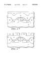
- FIG. 1is an enlarged cross-sectional view of a semiconductor device 10 according to a first embodiment of the present invention.
- Semiconductor device 10is preferably formed on a silicon substrate 11.
- semiconductor device 10is an n-channel device, although it will be understood that the present invention can be used to form p-channel devices by changing n-type conductivities to p-type and vice versa.
- portions of substrate 11are oxidized to grow field oxide regions 15.
- an oxidizing masksuch as silicon nitride
- portions of substrate 11are exposed to an oxygen rich ambient at about 800° C. to 1200° C.
- Field oxide regions 15are approximately 5,000 angstroms thick and provide electrical isolation for semiconductor device 10.
- the unoxidized portion of substrate 11 between field oxide regions 15is referred to as active area which is where semiconductor device 10 is formed.
- a gate structure 14is then patterned on substrate 11 which can comprise a silicon dioxide layer 12 with a thickness in the range from 50 angstroms to 1000 angstroms and a layer of polysilicon 13 which is 1,000 angstroms to 4,000 angstroms thick is deposited on silicon dioxide layer 12.
- a dielectric layer or a phosphorus doped PECVD film 16with a thickness of 1,000 angstroms to 5,000 angstroms, is then deposited over substrate 11 and gate structure 14 using a plasma enhanced chemical vapor deposition (PECVD) process using tetraethylorthosilicate (TEOS). During deposition, trimethylphosphite is added to produce a phosphorus concentration in dielectric layer 16.
- PECVDplasma enhanced chemical vapor deposition
- TEOStetraethylorthosilicate
- Substrate 11is placed in a PECVD reaction chamber under vacuum with a pressure of approximately 0.5 Torr to 75 Torr and a temperature of approximately 370° C. to 410° C.
- TEOS and trimethylphosphitewhich come from liquid sources, are introduced into the reaction chamber through a shower head and exposed to an RF generated plasma with a power level of 100 watts to 500 watts which creates the reactions required to form dielectric layer 16.
- the formation of dielectric layer 16is performed with a single deposition step through two reactions occurring simultaneously in the chamber, TEOS is decomposed to form silicon dioxide on substrate 11 and trimethylphosphite is simultaneously decomposed by the plasma to release phosphorus in such a form that it is incorporated into dielectric layer 16.
- the quantity of trimethylphosphite in the reaction chambercan be varied from 0.5 SCCM to 10 SCCM to provide a phosphorus concentration of 1 percent to 12 percent by weight.
- LPCVDlow pressure chemical vapor deposition
- phosphine gasis typically used to dope the silicon dioxide layer as it is deposited.
- trimethylphosphitewhich is a stable liquid that is not as toxic as phosphine gas, is used to dope dielectric layer 16. Since trimethylphosphite is much easier and safer to use than phosphine, it does not have the environmental issues associated with the use of phosphine gas.
- Trimethylphosphitealso offers an unexpected improvement in the conformality of dielectric layer 16 as it is deposited.
- Conformalitydescribes how accurately a process can deposit evenly over the top and sides of the structures, and is a function of the processing conditions and dopant concentration.
- the thickness of the film along vertical surfacesis divided by the thickness of the film along horizontal surfaces.
- Traditional LPCVD deposition techniques, which use phosphine dopanthave a significant variation in phosphorus concentration from one deposition to the next. This will affect both the accuracy of wet or dry etch steps that follow and will vary the conformality of the film deposited.
- phosphine doped LPCVD reactionscan only provide step coverage ratios of 30 percent.
- trimethylphosphiteprovides accurate control of the dopant concentration across the wafer and from wafer to wafer. It also allows for step coverage ratios in excess of 60 percent. As device geometries decrease, dielectric layers that can be deposited with high conformality ratios will become a necessity.
- An additional benefit of the present inventionis that the doped PECVD deposition is performed in a single wafer reaction chamber with a deposition rate of approximately 8,000 angstroms per minute. This offers a much more efficient process which will improve the throughput of a fabrication facility, especially for small lot sizes.
- CVD reactionstake place as a batch reaction with typically 100 to 200 wafers being processed simultaneously and offer a deposition rate on the order of 200 angstroms per minute.
- FIG. 2is an enlarged cross-sectional view of semiconductor device 10 after further processing.
- Dielectric layer 16is etched using a reactive ion etch (RIE) process to form sidewall spacers 17.
- RIEreactive ion etch
- the width of sidewall spacers 17 at the surface of substrate 11is determined by the conformality of dielectric layer 16 and the amount of etch and overetch performed during the RIE process.
- An anneal stepis then performed to activate the dopant in sidewall spacers 17 to form doped regions 19 under sidewall spacers 17.
- Substrate 11is heated to about 950° C. to 1100° C. for about 15 minutes to 60 minutes which will drive the phosphorus concentration from sidewall spacers 17 into substrate 11.
- the depth and concentration of doped regions 19can be controlled by the amount of trimethylphosphite used to form sidewall spacers 17 and the time and temperature of the anneal step.
- lightly doped drain regions under sidewall spacershad to be formed with an additional photoresist pattern and implant step.
- the present inventionprovides for the obviation of these steps by forming doped regions 19 with the out diffusion of phosphorus from sidewall spacers 17. This reduction of three process steps will reduce the manufacturing cost of semiconductor device 10. It is also possible to omit the above mentioned anneal step if doped regions 19 are not desired.
- Sidewall spacers 17can then be used to provide mobile ion protection for
- Source and drain regions 18are then used in conjunction with a patterned photoresist layer (not shown) to define source and drain regions 18 in substrate 11.
- Source and drain regions 18are formed by ion implanting with an n-type dopant such as arsenic into substrate 11.
- An arsenic dose of about 5.0 ⁇ 10 14 atoms/cm 2 to 1.0 ⁇ 10 15 atoms/cm 2 and an implant energy of about 30 keV to 100 keVis suitable to provide source and drain regions 18.
- Sidewall spacers 17are also used to prevent electrical shorts during the formation of silicide regions 20 on source and drain regions 18 and gate structure 14.
- a layer of refractory materialsuch as titanium, is deposited on semiconductor substrate 11 and gate structure 14.
- a rapid thermal anneal (RTA) stepat 600° C. to 700° C. for 30 seconds to 2 minutes is performed to react the titanium with the silicon of source and drain regions 18 and gate structure 14. Any remaining portions of the refractory material are then removed with a wet etch such as ammonium hydroxide and hydrogen peroxide.
- a second RTA stepat 750° C. to 950° C. for 10 seconds to 2 minutes is performed to lower the resistivity of silicide regions 20.
- sidewall spacers 17are formed from silicon dioxide, they will not react with the refractory material and thus electrically isolate gate structure 14 from source and drain regions 18. Since sidewall spacers 17 were doped using trimethylphosphite, they also provide protection to gate structure 14 from mobile ions such as sodium which can degrade the performance of semiconductor device 10. These mobile ions can be introduced into the semiconductor device from poor wafer handling or chemicals such as photoresist.
- FIG. 3is an enlarged cross-sectional view of a semiconductor device 30 according to a second embodiment of the present invention.
- a phosphorus doped PECVD film that was doped with trimethylphosphitecan also be used to form interlevel dielectric layers (ILD). Such a film offers mobile ion gettering properties and improved conformality over previously known films.
- ILDinterlevel dielectric layers
- portions of a silicon substrate 31are oxidized to form field oxide regions 28.
- an oxidizing masksuch as silicon nitride
- portions of substrate 31are exposed to an oxygen rich ambient at about 800° C. to 1200° C.
- Field oxide regions 28are approximately 5,000 angstroms thick and provide electrical isolation for semiconductor device 30.
- a gate structure 35is formed on substrate 31 by a silicon dioxide layer 32 with a thickness in the range from 50 angstroms to 1000 angstroms and a layer of polysilicon 33 is then formed on silicon dioxide layer 32 which is 1,000 angstroms to 4,000 angstroms thick.
- Sidewall spacers 34are formed adjacent to the edges of gate structure 35 using either the first embodiment of the present invention, or other techniques known in the art.
- Source and drain regions 36are formed in substrate 31 by implanting substrate 31 through a patterned photoresist layer which is aligned to sidewall spacers 34.
- undoped dielectric layer 37is then deposited over gate structure 35 and the surface of substrate 31.
- undoped dielectric layeris a 100 angstrom to 5,000 angstrom thick layer of silicon dioxide which is deposited with either a CVD or PECVD process.
- a doped PECVD layer 38is then deposited on undoped dielectric layer 37 using the method provided in the present invention.
- Dielectric layer 38is doped with trimethylphosphite during deposition to have a phosphorus concentration of 1 percent to 12 percent by weight.
- the thickness of dielectric layer 38can vary from 1,000 angstroms to 15,000 angstroms with a preferred thickness of 10,000 angstroms.
- Dielectric layer 38is then planarized to provide a relatively flat surface for the interconnect layers.
- One such methodfirst deposits a layer of photoresist 39 on dielectric layer 38.
- a plasma assisted etch using a fluorine based chemistryis used to etch photoresist layer 39 and portions of dielectric layer 38 at approximately the same rate.
- An optional oxygen based plasma assisted etchmay be used prior to the fluorine based etch to reduce the thickness of photoresist layer 39.
- This processwill form a relatively planar surface as shown in FIG. 4.
- Any remaining portions of photoresist layer 39are then stripped and a second photoresist layer 41 is patterned to define contact regions 48 shown in FIG. 5. It is also possible to planarize the surface of dielectric layer 38 with a chemical mechanical polishing process.
- RIE etchis used to remove the exposed portions of dielectric layer 38 and the underlying undoped dielectric layer 37 to form contact openings.
- Photoresist layer 41is then removed and a barrier metal or metal alloy such as titanium tungsten is deposited into the contact openings to form barrier layer 40.
- a metal layer 45using a material such as aluminum, is either sputtered or evaporated on barrier layer 40.
- a masking layer in conjunction with an RIE etchis used to form metallized contact regions 48 as shown in FIG. 5. Contacts 48 provide electrical connection to source and drain regions 36 and gate structure 35.
- the second embodiment of the present inventioncan be repeated to form a plurality of interlevel dielectric layers.
- trimethylphosphite doped filmshave reduced particulate counts compared to films which are deposited using traditional silane based LPCVD techniques. This is of even greater benefit when the present invention is used to form interlevel dielectric layers. As the thickness of the deposited layer increases, the density of particulates formed will increase, which could exponentially decrease the yield of devices fabricated. The present invention, therefore, can have an exponential improvement in functional yield.
- Trimethylphosphite doped filmsalso have an improved conformality over silane based films doped with phosphine sources, which reduces the likelihood of forming voids in the interlevel dielectric layers due to poor step coverage over high aspect ratio device topographies.
- Undoped dielectric layer 37 of semiconductor device 30is formed to prevent the diffusion of phosphorus from dielectric layer 38 into either gate structure 35 or substrate 31. In some applications, however, it may be either desirous or insignificant if dopant should diffuse out of dielectric layer 38 such as if dielectric layer 38 is used to form a second or third inter-level dielectric layer or if only n-channel devices are formed. In such an application, the present invention can be used to dope gate structure 35 and source and drain regions 36 with phosphorus from dielectric layer 38. The out diffusion of the phosphorus will reduce the resistivity of gate structure 35 and improve the conduction of source and drain regions 36.
- FIG. 6is an enlarged cross-sectional view of semiconductor device 30 according to a third embodiment of the present invention.
- the trimethylphosphite doped layerhas a phosphorus concentration which will getter mobile ions, it can also be used as a passivation layer 46 over semiconductor device 30.
- a 1,000 angstrom to 10,000 angstrom thick PECVD film doped with trimethylphosphiteis used to form passivation layer 46.
- the trimethylphosphite doped filmis deposited below the melting point of most metal films used in semiconductor applications. This property, coupled with the fact that a passivation layer can be formed with a single deposition step, make the present invention an efficient and cost effective solution for forming passivation layer 46.
- the present inventionprovides a method for forming a phosphorus doped dielectric layer using trimethylphosphite that has several applications in semiconductor device structures.
- the trimethylphosphiteis used while in a liquid phase and is not as toxic or environmentally hazardous has phosphine.
- the present inventionprovides the unexpected result of improved film conformality, improved control of phosphorus concentration from run to run, and reduced particulate counts over previously known methods for forming dielectric layers.
- the trimethylphosphite doped dielectric layeris formed in a single step deposition process at temperatures that are below that of most metallic films used in the semiconductor industry. Therefore, the present invention offers a lost cost, high throughput process that can be used in a variety of device structures such as sidewall spacers 17, interlevel dielectric layer 38, or a passivation layer 46.
Landscapes
- Engineering & Computer Science (AREA)
- Physics & Mathematics (AREA)
- Condensed Matter Physics & Semiconductors (AREA)
- General Physics & Mathematics (AREA)
- Manufacturing & Machinery (AREA)
- Computer Hardware Design (AREA)
- Microelectronics & Electronic Packaging (AREA)
- Power Engineering (AREA)
- Formation Of Insulating Films (AREA)
- Internal Circuitry In Semiconductor Integrated Circuit Devices (AREA)
Abstract
Description
Claims (10)
Priority Applications (1)
| Application Number | Priority Date | Filing Date | Title |
|---|---|---|---|
| US08/810,037US5814545A (en) | 1995-10-02 | 1997-03-04 | Semiconductor device having a phosphorus doped PECVD film and a method of manufacture |
Applications Claiming Priority (2)
| Application Number | Priority Date | Filing Date | Title |
|---|---|---|---|
| US53737895A | 1995-10-02 | 1995-10-02 | |
| US08/810,037US5814545A (en) | 1995-10-02 | 1997-03-04 | Semiconductor device having a phosphorus doped PECVD film and a method of manufacture |
Related Parent Applications (1)
| Application Number | Title | Priority Date | Filing Date |
|---|---|---|---|
| US53737895AContinuation | 1995-10-02 | 1995-10-02 |
Publications (1)
| Publication Number | Publication Date |
|---|---|
| US5814545Atrue US5814545A (en) | 1998-09-29 |
Family
ID=24142394
Family Applications (1)
| Application Number | Title | Priority Date | Filing Date |
|---|---|---|---|
| US08/810,037Expired - LifetimeUS5814545A (en) | 1995-10-02 | 1997-03-04 | Semiconductor device having a phosphorus doped PECVD film and a method of manufacture |
Country Status (1)
| Country | Link |
|---|---|
| US (1) | US5814545A (en) |
Cited By (18)
| Publication number | Priority date | Publication date | Assignee | Title |
|---|---|---|---|---|
| US5913124A (en)* | 1997-05-24 | 1999-06-15 | United Microelectronics Corporation | Method of making a self-aligned silicide |
| US6069044A (en)* | 1998-03-30 | 2000-05-30 | Texas Instruments-Acer Incorporated | Process to fabricate ultra-short channel nMOSFETS with self-aligned silicide contact |
| US6117719A (en)* | 1997-12-18 | 2000-09-12 | Advanced Micro Devices, Inc. | Oxide spacers as solid sources for gallium dopant introduction |
| EP1061567A1 (en)* | 1999-06-17 | 2000-12-20 | Mitsubishi Denki Kabushiki Kaisha | Method and apparatus for manufacturing an improved phosphosilicate glass film |
| US6225209B1 (en)* | 1998-05-16 | 2001-05-01 | United Microelectronics Corp. | Method of fabricating crack resistant inter-layer dielectric for a salicide process |
| EP1146014A3 (en)* | 2000-04-11 | 2002-04-03 | Applied Materials, Inc. | Mesoporous silica films with mobile ion gettering and accelerated processing |
| US6649308B1 (en)* | 1998-03-30 | 2003-11-18 | Texas Instruments-Acer Incorporated | Ultra-short channel NMOSFETS with self-aligned silicide contact |
| US6664172B2 (en)* | 2002-01-22 | 2003-12-16 | United Microelectronics Corp. | Method of forming a MOS transistor with improved threshold voltage stability |
| US20050153496A1 (en)* | 2004-01-12 | 2005-07-14 | Ngo Minh V. | Low stress sidewall spacer in integrated circuit technology |
| US20060240634A1 (en)* | 2003-09-17 | 2006-10-26 | Tran Luan C | DRAM access transistor and method of formation |
| US7825481B2 (en)* | 2005-02-23 | 2010-11-02 | Intel Corporation | Field effect transistor with narrow bandgap source and drain regions and method of fabrication |
| US20110020987A1 (en)* | 2003-06-27 | 2011-01-27 | Hareland Scott A | Nonplanar semiconductor device with partially or fully wrapped around gate electrode and methods of fabrication |
| US8071983B2 (en) | 2005-06-21 | 2011-12-06 | Intel Corporation | Semiconductor device structures and methods of forming semiconductor structures |
| US8193567B2 (en) | 2005-09-28 | 2012-06-05 | Intel Corporation | Process for integrating planar and non-planar CMOS transistors on a bulk substrate and article made thereby |
| US8502351B2 (en) | 2004-10-25 | 2013-08-06 | Intel Corporation | Nonplanar device with thinned lower body portion and method of fabrication |
| US8741733B2 (en) | 2008-06-23 | 2014-06-03 | Intel Corporation | Stress in trigate devices using complimentary gate fill materials |
| US10515801B2 (en) | 2007-06-04 | 2019-12-24 | Micron Technology, Inc. | Pitch multiplication using self-assembling materials |
| CN112951727A (en)* | 2019-12-10 | 2021-06-11 | 新唐科技股份有限公司 | Semiconductor device structure and method for manufacturing the same |
Citations (11)
| Publication number | Priority date | Publication date | Assignee | Title |
|---|---|---|---|---|
| US4621413A (en)* | 1985-06-03 | 1986-11-11 | Motorola, Inc. | Fabricating a semiconductor device with reduced gate leakage |
| WO1987007763A1 (en)* | 1986-06-16 | 1987-12-17 | American Telephone & Telegraph Company | Method for fabricating devices using chemical vapour deposition, and devices formed thereby |
| US4755478A (en)* | 1987-08-13 | 1988-07-05 | International Business Machines Corporation | Method of forming metal-strapped polysilicon gate electrode for FET device |
| US4807016A (en)* | 1985-07-15 | 1989-02-21 | Texas Instruments Incorporated | Dry etch of phosphosilicate glass with selectivity to undoped oxide |
| US4837179A (en)* | 1985-11-02 | 1989-06-06 | Plessey Overseas Limited | Method of making a LDD mosfet |
| US4892753A (en)* | 1986-12-19 | 1990-01-09 | Applied Materials, Inc. | Process for PECVD of silicon oxide using TEOS decomposition |
| US4948744A (en)* | 1986-06-30 | 1990-08-14 | Oki Electric Industry Co., Ltd. | Process of fabricating a MISFET |
| US5166101A (en)* | 1989-09-28 | 1992-11-24 | Applied Materials, Inc. | Method for forming a boron phosphorus silicate glass composite layer on a semiconductor wafer |
| EP0594298A1 (en)* | 1992-09-22 | 1994-04-27 | AT&T Corp. | Integrated circuit doped dielectric, preventing contamination by mobile ions |
| US5314845A (en)* | 1989-09-28 | 1994-05-24 | Applied Materials, Inc. | Two step process for forming void-free oxide layer over stepped surface of semiconductor wafer |
| US5393704A (en)* | 1993-12-13 | 1995-02-28 | United Microelectronics Corporation | Self-aligned trenched contact (satc) process |
- 1997
- 1997-03-04USUS08/810,037patent/US5814545A/ennot_activeExpired - Lifetime
Patent Citations (12)
| Publication number | Priority date | Publication date | Assignee | Title |
|---|---|---|---|---|
| US4621413A (en)* | 1985-06-03 | 1986-11-11 | Motorola, Inc. | Fabricating a semiconductor device with reduced gate leakage |
| US4807016A (en)* | 1985-07-15 | 1989-02-21 | Texas Instruments Incorporated | Dry etch of phosphosilicate glass with selectivity to undoped oxide |
| US4837179A (en)* | 1985-11-02 | 1989-06-06 | Plessey Overseas Limited | Method of making a LDD mosfet |
| WO1987007763A1 (en)* | 1986-06-16 | 1987-12-17 | American Telephone & Telegraph Company | Method for fabricating devices using chemical vapour deposition, and devices formed thereby |
| US4948744A (en)* | 1986-06-30 | 1990-08-14 | Oki Electric Industry Co., Ltd. | Process of fabricating a MISFET |
| US4892753A (en)* | 1986-12-19 | 1990-01-09 | Applied Materials, Inc. | Process for PECVD of silicon oxide using TEOS decomposition |
| US4755478A (en)* | 1987-08-13 | 1988-07-05 | International Business Machines Corporation | Method of forming metal-strapped polysilicon gate electrode for FET device |
| US5166101A (en)* | 1989-09-28 | 1992-11-24 | Applied Materials, Inc. | Method for forming a boron phosphorus silicate glass composite layer on a semiconductor wafer |
| US5314845A (en)* | 1989-09-28 | 1994-05-24 | Applied Materials, Inc. | Two step process for forming void-free oxide layer over stepped surface of semiconductor wafer |
| US5354387A (en)* | 1989-09-28 | 1994-10-11 | Applied Materials, Inc. | Boron phosphorus silicate glass composite layer on semiconductor wafer |
| EP0594298A1 (en)* | 1992-09-22 | 1994-04-27 | AT&T Corp. | Integrated circuit doped dielectric, preventing contamination by mobile ions |
| US5393704A (en)* | 1993-12-13 | 1995-02-28 | United Microelectronics Corporation | Self-aligned trenched contact (satc) process |
Non-Patent Citations (8)
| Title |
|---|
| Pillote, C., et al., "Characterization of Phosphosilicate . . .", Thin Solid Films, vol. 236, 1993, pp. 287-293. |
| Pillote, C., et al., Characterization of Phosphosilicate . . . , Thin Solid Films, vol. 236, 1993, pp. 287 293.* |
| Wolf, S., Silicon Processing, vol. 1, Lattice Press, 1986, pp. 182 187.* |
| Wolf, S., Silicon Processing, vol. 1, Lattice Press, 1986, pp. 182-187. |
| Wolf, S., Silicon Processing, vol. 1, Lattice Press, 1986, pp. 187 191, 397 399.* |
| Wolf, S., Silicon Processing, vol. 1, Lattice Press, 1986, pp. 187-191, 397-399. |
| Wolf, S., Silicon Processing, vol. 2, Lattice Press, 1990, pp. 222 228, 238 239.* |
| Wolf, S., Silicon Processing, vol. 2, Lattice Press, 1990, pp. 222-228, 238-239. |
Cited By (44)
| Publication number | Priority date | Publication date | Assignee | Title |
|---|---|---|---|---|
| US5913124A (en)* | 1997-05-24 | 1999-06-15 | United Microelectronics Corporation | Method of making a self-aligned silicide |
| US6117719A (en)* | 1997-12-18 | 2000-09-12 | Advanced Micro Devices, Inc. | Oxide spacers as solid sources for gallium dopant introduction |
| US6649308B1 (en)* | 1998-03-30 | 2003-11-18 | Texas Instruments-Acer Incorporated | Ultra-short channel NMOSFETS with self-aligned silicide contact |
| US6069044A (en)* | 1998-03-30 | 2000-05-30 | Texas Instruments-Acer Incorporated | Process to fabricate ultra-short channel nMOSFETS with self-aligned silicide contact |
| US6225209B1 (en)* | 1998-05-16 | 2001-05-01 | United Microelectronics Corp. | Method of fabricating crack resistant inter-layer dielectric for a salicide process |
| EP1061567A1 (en)* | 1999-06-17 | 2000-12-20 | Mitsubishi Denki Kabushiki Kaisha | Method and apparatus for manufacturing an improved phosphosilicate glass film |
| EP1146014A3 (en)* | 2000-04-11 | 2002-04-03 | Applied Materials, Inc. | Mesoporous silica films with mobile ion gettering and accelerated processing |
| US6664172B2 (en)* | 2002-01-22 | 2003-12-16 | United Microelectronics Corp. | Method of forming a MOS transistor with improved threshold voltage stability |
| US8273626B2 (en) | 2003-06-27 | 2012-09-25 | Intel Corporationn | Nonplanar semiconductor device with partially or fully wrapped around gate electrode and methods of fabrication |
| US20110020987A1 (en)* | 2003-06-27 | 2011-01-27 | Hareland Scott A | Nonplanar semiconductor device with partially or fully wrapped around gate electrode and methods of fabrication |
| US20070176232A1 (en)* | 2003-09-17 | 2007-08-02 | Tran Luan C | DRAM access transistor and method of formation |
| US7547604B2 (en)* | 2003-09-17 | 2009-06-16 | Micron Technology, Inc. | Method of forming a recessed gate structure on a substrate having insulating columns and removing said insulating columns after forming a conductive region of the gate structure |
| US20060240634A1 (en)* | 2003-09-17 | 2006-10-26 | Tran Luan C | DRAM access transistor and method of formation |
| US7518184B2 (en) | 2003-09-17 | 2009-04-14 | Micron Technology, Inc. | DRAM access transistor |
| US20050153496A1 (en)* | 2004-01-12 | 2005-07-14 | Ngo Minh V. | Low stress sidewall spacer in integrated circuit technology |
| JP2007518274A (en)* | 2004-01-12 | 2007-07-05 | アドバンスト・マイクロ・ディバイシズ・インコーポレイテッド | Low stress sidewall spacers in integrated circuit technology. |
| GB2425405A (en)* | 2004-01-12 | 2006-10-25 | Advanced Micro Devices Inc | Low stress sidewall spacer in integrated circuit technology |
| DE112004002638B4 (en)* | 2004-01-12 | 2009-11-26 | Advanced Micro Devices, Inc., Sunnyvale | Method of manufacturing an integrated circuit with low tension sidewall spacers |
| GB2425405B (en)* | 2004-01-12 | 2008-08-20 | Advanced Micro Devices Inc | Low stress sidewall spacer in integrated circuit technology |
| US7005357B2 (en) | 2004-01-12 | 2006-02-28 | Advanced Micro Devices, Inc. | Low stress sidewall spacer in integrated circuit technology |
| WO2005071729A1 (en)* | 2004-01-12 | 2005-08-04 | Advanced Micro Devices, Inc. | Low stress sidewall spacer in integrated circuit technology |
| US8502351B2 (en) | 2004-10-25 | 2013-08-06 | Intel Corporation | Nonplanar device with thinned lower body portion and method of fabrication |
| US9190518B2 (en) | 2004-10-25 | 2015-11-17 | Intel Corporation | Nonplanar device with thinned lower body portion and method of fabrication |
| US8749026B2 (en) | 2004-10-25 | 2014-06-10 | Intel Corporation | Nonplanar device with thinned lower body portion and method of fabrication |
| US10236356B2 (en) | 2004-10-25 | 2019-03-19 | Intel Corporation | Nonplanar device with thinned lower body portion and method of fabrication |
| US9741809B2 (en) | 2004-10-25 | 2017-08-22 | Intel Corporation | Nonplanar device with thinned lower body portion and method of fabrication |
| US7825481B2 (en)* | 2005-02-23 | 2010-11-02 | Intel Corporation | Field effect transistor with narrow bandgap source and drain regions and method of fabrication |
| US8368135B2 (en) | 2005-02-23 | 2013-02-05 | Intel Corporation | Field effect transistor with narrow bandgap source and drain regions and method of fabrication |
| US9048314B2 (en) | 2005-02-23 | 2015-06-02 | Intel Corporation | Field effect transistor with narrow bandgap source and drain regions and method of fabrication |
| US8664694B2 (en) | 2005-02-23 | 2014-03-04 | Intel Corporation | Field effect transistor with narrow bandgap source and drain regions and method of fabrication |
| US9368583B2 (en) | 2005-02-23 | 2016-06-14 | Intel Corporation | Field effect transistor with narrow bandgap source and drain regions and method of fabrication |
| US8183646B2 (en) | 2005-02-23 | 2012-05-22 | Intel Corporation | Field effect transistor with narrow bandgap source and drain regions and method of fabrication |
| US8816394B2 (en) | 2005-02-23 | 2014-08-26 | Intel Corporation | Field effect transistor with narrow bandgap source and drain regions and method of fabrication |
| US7893506B2 (en) | 2005-02-23 | 2011-02-22 | Intel Corporation | Field effect transistor with narrow bandgap source and drain regions and method of fabrication |
| US8071983B2 (en) | 2005-06-21 | 2011-12-06 | Intel Corporation | Semiconductor device structures and methods of forming semiconductor structures |
| US8933458B2 (en) | 2005-06-21 | 2015-01-13 | Intel Corporation | Semiconductor device structures and methods of forming semiconductor structures |
| US9385180B2 (en) | 2005-06-21 | 2016-07-05 | Intel Corporation | Semiconductor device structures and methods of forming semiconductor structures |
| US8581258B2 (en) | 2005-06-21 | 2013-11-12 | Intel Corporation | Semiconductor device structures and methods of forming semiconductor structures |
| US9761724B2 (en) | 2005-06-21 | 2017-09-12 | Intel Corporation | Semiconductor device structures and methods of forming semiconductor structures |
| US8193567B2 (en) | 2005-09-28 | 2012-06-05 | Intel Corporation | Process for integrating planar and non-planar CMOS transistors on a bulk substrate and article made thereby |
| US10515801B2 (en) | 2007-06-04 | 2019-12-24 | Micron Technology, Inc. | Pitch multiplication using self-assembling materials |
| US9224754B2 (en) | 2008-06-23 | 2015-12-29 | Intel Corporation | Stress in trigate devices using complimentary gate fill materials |
| US8741733B2 (en) | 2008-06-23 | 2014-06-03 | Intel Corporation | Stress in trigate devices using complimentary gate fill materials |
| CN112951727A (en)* | 2019-12-10 | 2021-06-11 | 新唐科技股份有限公司 | Semiconductor device structure and method for manufacturing the same |
Similar Documents
| Publication | Publication Date | Title |
|---|---|---|
| US5814545A (en) | Semiconductor device having a phosphorus doped PECVD film and a method of manufacture | |
| US5304510A (en) | Method of manufacturing a multilayered metallization structure in which the conductive layer and insulating layer are selectively deposited | |
| US5723893A (en) | Method for fabricating double silicide gate electrode structures on CMOS-field effect transistors | |
| US5945350A (en) | Methods for use in formation of titanium nitride interconnects and interconnects formed using same | |
| US5393685A (en) | Peeling free metal silicide films using rapid thermal anneal | |
| US6133150A (en) | Semiconductor device and method for manufacturing the same | |
| US5234850A (en) | Method of fabricating a nitride capped MOSFET for integrated circuits | |
| US5089432A (en) | Polycide gate MOSFET process for integrated circuits | |
| EP0843348B1 (en) | Method and apparatus for processing a semiconductor substrate | |
| US5541131A (en) | Peeling free metal silicide films using ion implantation | |
| US6294476B1 (en) | Plasma surface treatment method for forming patterned TEOS based silicon oxide layer with reliable via and interconnection formed therethrough | |
| EP0126424A2 (en) | Process for making polycide structures | |
| US5130266A (en) | Polycide gate MOSFET process for integrated circuits | |
| US6358859B1 (en) | HBr silicon etching process | |
| KR20010063781A (en) | Fabricating method for semiconductor device | |
| US6530380B1 (en) | Method for selective oxide etching in pre-metal deposition | |
| US5214305A (en) | Polycide gate MOSFET for integrated circuits | |
| US20210175075A1 (en) | Oxygen radical assisted dielectric film densification | |
| US20020025666A1 (en) | Use of selective ozone teos oxide to create variable thickness layers and spacers | |
| US5652172A (en) | Method for controlling the etch profile of an aperture formed through a multi-layer insulator layer | |
| US6303496B1 (en) | Methods of filling constrained spaces with insulating materials and/or of forming contact holes and/or contacts in an integrated circuit | |
| US5411907A (en) | Capping free metal silicide integrated process | |
| US20070022941A1 (en) | Method of forming a layer and method of manufacturing a semiconductor device using the same | |
| US6281146B1 (en) | Plasma enhanced chemical vapor deposition (PECVD) method for forming microelectronic layer with enhanced film thickness uniformity | |
| EP0066675B1 (en) | Processes for the fabrication of field effect transistors |
Legal Events
| Date | Code | Title | Description |
|---|---|---|---|
| STCF | Information on status: patent grant | Free format text:PATENTED CASE | |
| FPAY | Fee payment | Year of fee payment:4 | |
| AS | Assignment | Owner name:FREESCALE SEMICONDUCTOR, INC., TEXAS Free format text:ASSIGNMENT OF ASSIGNORS INTEREST;ASSIGNOR:MOTOROLA, INC.;REEL/FRAME:015698/0657 Effective date:20040404 Owner name:FREESCALE SEMICONDUCTOR, INC.,TEXAS Free format text:ASSIGNMENT OF ASSIGNORS INTEREST;ASSIGNOR:MOTOROLA, INC.;REEL/FRAME:015698/0657 Effective date:20040404 | |
| FPAY | Fee payment | Year of fee payment:8 | |
| AS | Assignment | Owner name:CITIBANK, N.A. AS COLLATERAL AGENT, NEW YORK Free format text:SECURITY AGREEMENT;ASSIGNORS:FREESCALE SEMICONDUCTOR, INC.;FREESCALE ACQUISITION CORPORATION;FREESCALE ACQUISITION HOLDINGS CORP.;AND OTHERS;REEL/FRAME:018855/0129 Effective date:20061201 Owner name:CITIBANK, N.A. AS COLLATERAL AGENT,NEW YORK Free format text:SECURITY AGREEMENT;ASSIGNORS:FREESCALE SEMICONDUCTOR, INC.;FREESCALE ACQUISITION CORPORATION;FREESCALE ACQUISITION HOLDINGS CORP.;AND OTHERS;REEL/FRAME:018855/0129 Effective date:20061201 | |
| FPAY | Fee payment | Year of fee payment:12 | |
| AS | Assignment | Owner name:CITIBANK, N.A., AS COLLATERAL AGENT,NEW YORK Free format text:SECURITY AGREEMENT;ASSIGNOR:FREESCALE SEMICONDUCTOR, INC.;REEL/FRAME:024397/0001 Effective date:20100413 Owner name:CITIBANK, N.A., AS COLLATERAL AGENT, NEW YORK Free format text:SECURITY AGREEMENT;ASSIGNOR:FREESCALE SEMICONDUCTOR, INC.;REEL/FRAME:024397/0001 Effective date:20100413 | |
| AS | Assignment | Owner name:CITIBANK, N.A., AS NOTES COLLATERAL AGENT, NEW YORK Free format text:SECURITY AGREEMENT;ASSIGNOR:FREESCALE SEMICONDUCTOR, INC.;REEL/FRAME:030633/0424 Effective date:20130521 Owner name:CITIBANK, N.A., AS NOTES COLLATERAL AGENT, NEW YOR Free format text:SECURITY AGREEMENT;ASSIGNOR:FREESCALE SEMICONDUCTOR, INC.;REEL/FRAME:030633/0424 Effective date:20130521 | |
| AS | Assignment | Owner name:CITIBANK, N.A., AS NOTES COLLATERAL AGENT, NEW YORK Free format text:SECURITY AGREEMENT;ASSIGNOR:FREESCALE SEMICONDUCTOR, INC.;REEL/FRAME:031591/0266 Effective date:20131101 Owner name:CITIBANK, N.A., AS NOTES COLLATERAL AGENT, NEW YOR Free format text:SECURITY AGREEMENT;ASSIGNOR:FREESCALE SEMICONDUCTOR, INC.;REEL/FRAME:031591/0266 Effective date:20131101 | |
| AS | Assignment | Owner name:FREESCALE SEMICONDUCTOR, INC., TEXAS Free format text:PATENT RELEASE;ASSIGNOR:CITIBANK, N.A., AS COLLATERAL AGENT;REEL/FRAME:037356/0553 Effective date:20151207 Owner name:FREESCALE SEMICONDUCTOR, INC., TEXAS Free format text:PATENT RELEASE;ASSIGNOR:CITIBANK, N.A., AS COLLATERAL AGENT;REEL/FRAME:037354/0225 Effective date:20151207 Owner name:FREESCALE SEMICONDUCTOR, INC., TEXAS Free format text:PATENT RELEASE;ASSIGNOR:CITIBANK, N.A., AS COLLATERAL AGENT;REEL/FRAME:037356/0143 Effective date:20151207 | |
| AS | Assignment | Owner name:MORGAN STANLEY SENIOR FUNDING, INC., MARYLAND Free format text:ASSIGNMENT AND ASSUMPTION OF SECURITY INTEREST IN PATENTS;ASSIGNOR:CITIBANK, N.A.;REEL/FRAME:037486/0517 Effective date:20151207 | |
| AS | Assignment | Owner name:MORGAN STANLEY SENIOR FUNDING, INC., MARYLAND Free format text:ASSIGNMENT AND ASSUMPTION OF SECURITY INTEREST IN PATENTS;ASSIGNOR:CITIBANK, N.A.;REEL/FRAME:037518/0292 Effective date:20151207 | |
| AS | Assignment | Owner name:NXP, B.V., F/K/A FREESCALE SEMICONDUCTOR, INC., NETHERLANDS Free format text:RELEASE BY SECURED PARTY;ASSIGNOR:MORGAN STANLEY SENIOR FUNDING, INC.;REEL/FRAME:040925/0001 Effective date:20160912 Owner name:NXP, B.V., F/K/A FREESCALE SEMICONDUCTOR, INC., NE Free format text:RELEASE BY SECURED PARTY;ASSIGNOR:MORGAN STANLEY SENIOR FUNDING, INC.;REEL/FRAME:040925/0001 Effective date:20160912 | |
| AS | Assignment | Owner name:NXP B.V., NETHERLANDS Free format text:RELEASE BY SECURED PARTY;ASSIGNOR:MORGAN STANLEY SENIOR FUNDING, INC.;REEL/FRAME:040928/0001 Effective date:20160622 | |
| AS | Assignment | Owner name:MORGAN STANLEY SENIOR FUNDING, INC., MARYLAND Free format text:CORRECTIVE ASSIGNMENT TO CORRECT THE REMOVE PATENTS 8108266 AND 8062324 AND REPLACE THEM WITH 6108266 AND 8060324 PREVIOUSLY RECORDED ON REEL 037518 FRAME 0292. ASSIGNOR(S) HEREBY CONFIRMS THE ASSIGNMENT AND ASSUMPTION OF SECURITY INTEREST IN PATENTS;ASSIGNOR:CITIBANK, N.A.;REEL/FRAME:041703/0536 Effective date:20151207 | |
| AS | Assignment | Owner name:SHENZHEN XINGUODU TECHNOLOGY CO., LTD., CHINA Free format text:CORRECTIVE ASSIGNMENT TO CORRECT THE TO CORRECT THE APPLICATION NO. FROM 13,883,290 TO 13,833,290 PREVIOUSLY RECORDED ON REEL 041703 FRAME 0536. ASSIGNOR(S) HEREBY CONFIRMS THE THE ASSIGNMENT AND ASSUMPTION OF SECURITYINTEREST IN PATENTS.;ASSIGNOR:MORGAN STANLEY SENIOR FUNDING, INC.;REEL/FRAME:048734/0001 Effective date:20190217 | |
| AS | Assignment | Owner name:MORGAN STANLEY SENIOR FUNDING, INC., MARYLAND Free format text:CORRECTIVE ASSIGNMENT TO CORRECT THE REMOVE APPLICATION11759915 AND REPLACE IT WITH APPLICATION 11759935 PREVIOUSLY RECORDED ON REEL 037486 FRAME 0517. ASSIGNOR(S) HEREBY CONFIRMS THE ASSIGNMENT AND ASSUMPTION OF SECURITYINTEREST IN PATENTS;ASSIGNOR:CITIBANK, N.A.;REEL/FRAME:053547/0421 Effective date:20151207 | |
| AS | Assignment | Owner name:NXP B.V., NETHERLANDS Free format text:CORRECTIVE ASSIGNMENT TO CORRECT THE REMOVEAPPLICATION 11759915 AND REPLACE IT WITH APPLICATION11759935 PREVIOUSLY RECORDED ON REEL 040928 FRAME 0001. ASSIGNOR(S) HEREBY CONFIRMS THE RELEASE OF SECURITYINTEREST;ASSIGNOR:MORGAN STANLEY SENIOR FUNDING, INC.;REEL/FRAME:052915/0001 Effective date:20160622 | |
| AS | Assignment | Owner name:NXP, B.V. F/K/A FREESCALE SEMICONDUCTOR, INC., NETHERLANDS Free format text:CORRECTIVE ASSIGNMENT TO CORRECT THE REMOVEAPPLICATION 11759915 AND REPLACE IT WITH APPLICATION11759935 PREVIOUSLY RECORDED ON REEL 040925 FRAME 0001. ASSIGNOR(S) HEREBY CONFIRMS THE RELEASE OF SECURITYINTEREST;ASSIGNOR:MORGAN STANLEY SENIOR FUNDING, INC.;REEL/FRAME:052917/0001 Effective date:20160912 |