US5814239A - Gas-phase etching and regrowth method for Group III-nitride crystals - Google Patents
Gas-phase etching and regrowth method for Group III-nitride crystalsDownload PDFInfo
- Publication number
- US5814239A US5814239AUS08/684,608US68460896AUS5814239AUS 5814239 AUS5814239 AUS 5814239AUS 68460896 AUS68460896 AUS 68460896AUS 5814239 AUS5814239 AUS 5814239A
- Authority
- US
- United States
- Prior art keywords
- gas
- group iii
- etching
- nitride crystal
- phase etchant
- Prior art date
- Legal status (The legal status is an assumption and is not a legal conclusion. Google has not performed a legal analysis and makes no representation as to the accuracy of the status listed.)
- Expired - Lifetime
Links
Images


Classifications
- C—CHEMISTRY; METALLURGY
- C23—COATING METALLIC MATERIAL; COATING MATERIAL WITH METALLIC MATERIAL; CHEMICAL SURFACE TREATMENT; DIFFUSION TREATMENT OF METALLIC MATERIAL; COATING BY VACUUM EVAPORATION, BY SPUTTERING, BY ION IMPLANTATION OR BY CHEMICAL VAPOUR DEPOSITION, IN GENERAL; INHIBITING CORROSION OF METALLIC MATERIAL OR INCRUSTATION IN GENERAL
- C23F—NON-MECHANICAL REMOVAL OF METALLIC MATERIAL FROM SURFACE; INHIBITING CORROSION OF METALLIC MATERIAL OR INCRUSTATION IN GENERAL; MULTI-STEP PROCESSES FOR SURFACE TREATMENT OF METALLIC MATERIAL INVOLVING AT LEAST ONE PROCESS PROVIDED FOR IN CLASS C23 AND AT LEAST ONE PROCESS COVERED BY SUBCLASS C21D OR C22F OR CLASS C25
- C23F4/00—Processes for removing metallic material from surfaces, not provided for in group C23F1/00 or C23F3/00
- H—ELECTRICITY
- H01—ELECTRIC ELEMENTS
- H01L—SEMICONDUCTOR DEVICES NOT COVERED BY CLASS H10
- H01L21/00—Processes or apparatus adapted for the manufacture or treatment of semiconductor or solid state devices or of parts thereof
- H01L21/02—Manufacture or treatment of semiconductor devices or of parts thereof
- H01L21/04—Manufacture or treatment of semiconductor devices or of parts thereof the devices having potential barriers, e.g. a PN junction, depletion layer or carrier concentration layer
- H01L21/18—Manufacture or treatment of semiconductor devices or of parts thereof the devices having potential barriers, e.g. a PN junction, depletion layer or carrier concentration layer the devices having semiconductor bodies comprising elements of Group IV of the Periodic Table or AIIIBV compounds with or without impurities, e.g. doping materials
- H01L21/30—Treatment of semiconductor bodies using processes or apparatus not provided for in groups H01L21/20 - H01L21/26
- H01L21/302—Treatment of semiconductor bodies using processes or apparatus not provided for in groups H01L21/20 - H01L21/26 to change their surface-physical characteristics or shape, e.g. etching, polishing, cutting
- H01L21/306—Chemical or electrical treatment, e.g. electrolytic etching
- H01L21/30604—Chemical etching
- H01L21/30612—Etching of AIIIBV compounds
- H01L21/30621—Vapour phase etching
Definitions
- the inventionrelates to a method for gas-phase etching Group III-nitride crystals to produce an etched surface having an excellent surface quality.
- the inventionalso relates to a regrowth method that is performed after the gas-phase etching.
- the inventionrelates to a method of gas-phase etching and regrowth for Group III-nitride crystals.
- the methodcan be used to fabricate diodes or semiconductor lasers that emit ultraviolet to green light, light detectors, transistors for use at high temperatures, and semiconductor elements. Additionally, the methods according to the invention are well suited for use in mass production, are low in cost and result in high yields.
- Group III-nitride crystalssuch as GaN are extremely difficult to etch.
- a variety of etching methodshave been proposed. These methods are broadly classified into wet etching and dry etching. For example, wet etching places the surface of the GaN crystal to be etched in contact with a wet etchant, such as sodium hydroxide solution.
- the surface of the GaN crystal to be etchedis irradiated with a plasma of ions, for example, Ar ions.
- dry etchinguses a mechanical etchant instead of a chemical etchant, and has a fast etch rate.
- dry etchingnot only results in a rough etched surface, but also tends to damage the structure of the crystal. This leads to a concern that devices made from a crystal whose structure has been damaged by dry etching will have degraded operating characteristics and a shortened lifetime.
- the methodshould have a rapid etch rate, produce a smooth etched surface and should not damage the structure of the crystal.
- the inventionprovides a method for gas-phase etching Group III-nitride crystals.
- the methoddoes not use plasma irradiation in contrast to the conventional dry etching technologies described above.
- the present inventionprovides a method for gas-phase etching Group III-nitride crystals that does not damage the crystal structure, and that produces an etched surface with excellent surface quality and on which high-quality regrowth is possible.
- the method according to the inventioncan be used in fabricating light-emitting diodes or semiconductor lasers that emit ultraviolet to green light, light detectors, transistors for use at high temperatures, and other semiconductor elements. The method is well suited for use in mass production, has low cost and results in a high yield.
- the present inventionalso provides a method in which regrowth is performed on the etched surface immediately after the etching operation and results in high performance elements.
- a gas-phase etchantin the gas-phase etching method according to the present invention, includes at least one halogen in gaseous form and/or at least one hydrogen halide in gaseous form.
- a Group III-nitride crystalis heated to a temperature in the range of 500°-900° C. and is etched in a flow of the gas-phase etchant.
- the gas-phase etchantmay additionally include hydrogen.
- the gas-phase etchantmay alternatively be diluted with inert gas, and the Group III-nitride crystal may be etched in a flow of the gas-phase etchant diluted with the inert gas.
- the regrowth method of the present inventionregrowth is immediately performed on the etched surface provided by the gas-phase etching method of the present invention. Since the gas-phase etching method according to the invention is compatible with the type of reactor used to perform MOCVD or HVPE, the regrowth can be performed in the same reactor as that in which the gas-phase etching was performed. Performing the etching and the regrowth in the same reactor saves having to transfer the newly-etched crystal to another reactor to perform the regrowth, and reduces the risk of contamination of the etched surface prior to the regrowth being performed.
- the gas-phase etching and regrowth method according to the present inventioncan be applied to such Group III-nitride crystals as GaN, AlN, InN, GaInN, AlInN, AlGaN, AlGaInN, or BAlGaInN.
- Group III-nitride crystalsas GaN, AlN, InN, GaInN, AlInN, AlGaN, AlGaInN, or BAlGaInN.
- the gas-phase etchantmay be composed of at least one of the halogens, i.e., F 2 , Cl 2 , Br 2 , and I 2 , in gaseous form, and/or at least one of the hydrogen halides, i.e., HF, HCl, HBr, and HI, in gaseous form, with or without hydrogen.
- the halogensi.e., F 2 , Cl 2 , Br 2 , and I 2
- the hydrogen halidesi.e., HF, HCl, HBr, and HI
- the inert gas used for diluting the gas-phase etchantcan be N 2 , He, or Ar.
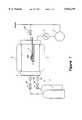
- FIG. 1is a schematic view of an example of a reactor that can be used to perform the gas-phase etching method according to the present invention.
- FIG. 2shows how an etch mask is applied to the sample prior to etching using the gas-phase etching method according to the present invention.
- FIG. 3shows the sample prepared by the masking method shown in FIG. 2.
- FIG. 4shows the sample illustrated in FIG. 3 after it has been etched using the gas-phase etching method according to the present invention.
- FIG. 5Ais a copy from a video printer (150 ⁇ magnification) of the etched surface obtained using the gas-phase etching method according to the present invention.
- FIG. 5Bis a copy of a photomicrograph of the etched surface obtained using a conventional etching method.
- FIG. 6shows how the etching depth measured after one hour varies with the concentration of the HCl gas in the gas-phase etchant at a given temperature.
- the gas-phase etching method according to the invention for Group III-nitride crystalsprovides an excellent etched surface quality by etching the Group III-nitride crystal under specific high temperature conditions in flow of a specific gas-phase etchant that includes specific components. No plasma irradiation is used in the gas-phase etching method according to the invention.
- the gas-phase etching method according to the inventioncan be easily be performed using the same type of reactor as is used for performing MOCVD or HVPE. This enables regrowth to be performed using MOCVD or HVPE immediately after the etched surface has been formed without having to transfer the Group III-nitride crystal to another reactor. Using the same reactor prevents an oxide film or a carbon film, which would obstruct regrowth, from being formed on the etched surface, and prevents contamination of the regrowth interface with impurities.
- a gas-phase etchantin the gas-phase etching method according to the present invention, includes at least one halogen in gaseous form and/or at least one hydrogen halide in gaseous form.
- a Group III-nitride crystalis heated to a temperature in the range of 500°-900° C. and is etched in a flow of the gas-phase etchant.
- the gas-phase etchantmay additionally include hydrogen.
- the gas-phase etchantmay alternatively be diluted with inert gas, and the Group III-nitride crystal may be etched in a flow of the gas-phase etchant diluted with the inert gas.
- the regrowth method of the present inventionenables regrowth to be immediately performed on the etched surface provided by the gas-phase etching method of the present invention.
- the gas-phase etchantmay be composed of at least one of the halogens, i.e., F 2 , Cl 2 , Br 2 , and I 2 , in gaseous form, and/or at least of the hydrogen halides, i.e., HF, HCl, HBr, and HI, in gaseous form, with, or without, hydrogen.
- the halogensi.e., F 2 , Cl 2 , Br 2 , and I 2
- the hydrogen halidesi.e., HF, HCl, HBr, and HI
- the inert gas used for diluting the gas-phase etchantcan be N 2 , He, or Ar.
- the gas-phase etchantwhen the gas-phase etchant includes hydrogen and at least one halogen in gaseous form and/or at least one hydrogen halide in gaseous form, the gas-phase etchant etches the Group-III nitride crystal using the reactions described by the formulas (a) and/or (b) shown below.
- the preferred mixture ratios of the constituents of the gas-phase etchantare those which provide the quantities of halogen and hydrogen that are needed in the reactions described by formulas (a) and (b).
- GaNis used as an example of the Group III-nitride.
- ammonia (NH 3 ) generated in the reactions described by the formulas (a) and (b)further reacts with the halogen and the hydrogen or the hydrogen halide of the gas-phase etchant to generate ammonium halide (NH 4 X). Therefore, is is preferable that the mixture ratio be determined to take account of the additional quantities of halogen, hydrogen, and/or hydrogen halide consumed by this additional reaction.
- the fraction of the at least one halogen in gaseous form and/or at least one hydrogen halide in gaseous form in the gas-phase etchantis between 0.001 vol % and 100 vol %, and is preferably between 0.1 vol % and 10 vol %.
- the constituent gases of the gas-phase etchantmay be mixed prior to supplying the gas-phase etchant to the reactor in which etching is carried out.
- the constituent gasesmay be supplied to the reactor separately and mixing to form the gas-phase etchant may occur in the reactor.
- the flow rate of the gas-phase etchant supplied to the reactorshould be that which causes the above-mentioned etching reaction to proceed at such a rate that the GaX 3 or NH 3 by-products generated by the reaction can easily be exhausted from the reactor.
- the rate at which the reaction by-products are exhausted from the reactoris related to the characteristics of the equipment used (for example, the size of the reaction pipe and/or the performance of the exhaust system), the size of the Group III-nitride crystal being etched, and the amount of etching.
- a flow rate in the range of about 0.1 milliliters per second (ml/s) to 10 liters per second (l/s)is preferred for the gas-phase etchant when a reaction pipe diameter of 80 mm is used in the present invention.
- the Group III-nitride crystalcan be etched using the reaction described in formula (b) set forth above.
- the present inventionis not limited to a gas-phase etchant that includes hydrogen, as described above.
- the gas-phase etchantcan include at least one halogen in gaseous form, in which case, the etching process is described by formula (c):
- the flow rate of the gas-phase etchantis similar to the flow rate of the gas-phase etchant including hydrogen described above.
- the reaction pipe diameteris 80 mm, a flow rate in the range of 0.1 ml/s to 10 l/s is preferred.
- the gas-phase etchantcan be diluted by an inert gas.
- the fraction of the gas-phase etchant in the gas-phase etchant diluted with inert gasis between 0.001 vol % and 100 vol %, and is preferably between 0.1 vol % and 20 vol %.
- gas-phase etchants described aboveirrespective of whether they are diluted with inert gas, are preferably used at atmospheric pressure, but excellent etching of Group III-nitride crystals can still be obtained at lower or higher pressures.
- performing the etch at atmospheric pressureprovides advantages in terms of manufacturing cost.
- the regrowth method according to the present inventionshould be performed immediately after a surface of the Group III-Nitride crystal has been etched using the gas-phase etching method according to the present invention described above.
- the basic structure of the reactor used for performing the gas-phase etching method according to the present inventionis the same as that of the reactor used to perform conventional regrowth methods such as MOCVD or HVPE. Consequently, after the gas-phase etching according to the present invention has been completed, the Group III-nitride crystal with the etched surface is not removed from the reactor in which the gas-phase etching was performed, but is then immediately subject to the regrowth method according to the present invention.
- etching and regrowthcan be performed in the same reactor.
- the regrowth methodis performed on the Group III-nitride crystal after it has been etched without removing the crystal from the reactor and without allowing the etched surface to come into contact with the atmosphere. This prevents such problems as the growth of an oxide film or a carbon film on the etched surface, which obstructs regrowth, or the introduction of impurities at the regrowth interface.
- the reactor shown in FIG. 1, for example,can be used to perform the gas-phase etching and regrowth method according to the present invention using any of the gas-phase etchants described above.
- the gas-phase etching and regrowth method according to the inventionis performed according to the following procedure. Two gas cylinders 71 and 72, inert gas cylinders (not shown), and a supply source (not shown) of each type of material needed during regrowth are set up. Gas from the gas cylinders 71 and 72, and the inert gas cylinders are mixed in the specified ratios and are diluted, if necessary, immediately before being introduced to the reactor 1.
- the procedure used when the gas-phase etchant includes hydrogen, as described above,will now be described.
- the gas cylinder 71contains at least one halogen in gaseous form and/or at least one hydrogen halide in gaseous form.
- the gas cylinder 72contains hydrogen. Since halogens and hydrogen halides are corrosive, the gas in the gas cylinder 71 may be diluted with hydrogen or a suitable inert gas.
- the Group III-nitride crystal 100 grown on a substrate such as sapphireis loaded on the susceptor 2 provided in the reactor 1.
- a GaN crystalwill be used as an example of the Group III-nitride crystal 100.
- the method according to the inventioncan applied to any Group III-nitride crystal.
- the thermocouple 3is set to measure the temperature of the crystal 100 on the susceptor 2.
- the GaN crystal 100Prior to etching, the GaN crystal 100 is masked by suitable masking material to define the parts of the crystal that will be etched.
- suitable masking materialFor example, SiO 2 or a two-layer film of Au (top layer) and Ti (bottom layer) may be used as the masking material.
- the valve 4is opened, and the vacuum pump 5 is operated to exhaust the interior of the reactor 1.
- the valve 4is then closed, and the valve 61 and/or the valve 62 are opened to supply the gas in the gas cylinders 71 and/or 72 to the interior of the reactor. This purges the interior of the reactor.
- the pressure in the reactor 1 during the purge operation and the subsequent etching operationis set to atmospheric pressure by keeping the valves 61, 62 and 63 open, and using the mass flow controllers 91 and 92 to adjust the flow rates of the gases constituting the gas-phase etchant so that a steady flow of the gas-phase etchant is provided at substantially atmospheric pressure.
- the interior of the reactor 1is heated by the heat source 8 placed in or near the reactor.
- the GaN crystal 100is heated, its temperature is measured by the thermocouple 3. Heating continues until the GaN crystal reaches a specified temperature within the range of 500° to 950° C.
- the gases constituting the gas-phase etchantetch the GaN crystal according to the reactions defined by the formulas (a) and/or (b) set forth above.
- the GaN crystalis etched where its surface is not masked and contacts the gas-phase etchant.
- the NH 3 generated by the etching reactionreacts again with the gas-phase etchant in the reactor 1 to form NH 4 X.
- the NH 4 X, any NH 3 that did not react with the gas-phase etchant, the GaX 3 and any other volatile compounds created by the etching reactionare discharged to the outside through valve 63 along with excess gas-phase etchant (primarily, hydrogen) not consumed by the etching reaction.
- the reactor 1has the same basic structure as the reactor used for performing MOCVD or HVPE, when MOCVD or HVPE is performed to perform the regrowth method according to the present invention on the etched surface as described above, the GaN crystal 100 can remain loaded on the susceptor 2 at the end of the etching process. The GaN crystal 100 can then undergo regrowth by MOCVD or HVPE without being removed from the reactor 1.
- the MOCVD or HVPE process used to perform the regrowth on the etched surfaceis conventional and so will not be described here.
- the procedure for etching the GaN crystal 100 using the gas-phase etchant including at least one halogen in gaseous form and/or at least one hydrogen halide in gaseous formwill be described next. Since this procedure is almost identical to that using the gas-phase etchant including at least one halogen in gaseous form and/or at least one hydrogen halide in gaseous form and additionally including hydrogen, only the parts of the procedure that are different will be described.
- the gas cylinder 71will be regarded as being the gas cylinder that contains the at least one halogen in gaseous form and/or at least one hydrogen halide in gaseous form.
- the at least one halogen in gaseous form and/or at least one hydrogen halide in gaseous formis introduced into the reactor 1 from the gas cylinder 71 by opening the valves 61 and 63.
- the at least one halogen in gaseous form and/or at least one hydrogen halide in gaseous form constituting the gas-phase etchantetch the GaN crystal according to the reactions defined by the formulas (b) and/or (c) set forth above, depending on the gas-phase etchant used.
- the GaN crystalis etched where its surface is not masked and contacts the gas-phase etchant.
- the NH 3 created by the etching reactionfurther reacts with the gas-phase etchant in the reactor 1 and becomes ammonium halide NH 4 X.
- the NH 4 X, NH 3 , GaX 3 , N 2 , and other products of the reactionare discharged outside the reactor through the valve 63, together with the excess gas-phase etchant that was not consumed by the etching reaction.
- the regrowth method according to the present inventioncan be performed on the newly-etched surface of the GaN crystal 100 by MOCVD or HVPE after the above-described etching method has been performed. Similar to when the gas-phase etchant additionally includes hydrogen, the regrowth can be performed without removing the GaN crystal 100 from the susceptor 2 inside the reactor 1.
- an additional gas cylinder(not shown) filled with the inert gas to be used for diluting the gas-phase etchant is provided in addition to the gas cylinders 71 and 72.
- the gas cylinders 71 and 72can be filled with the respective gases diluted with inert gas.
- the GaN crystal 100is etched by adjusting the relative rates of flow of gas from the cylinders 71 and 72 and the additional gas cylinder to establish the specified mixture ratio and dilution ratio of the gas-phase etchant immediately before introduction into the reactor 1.
- the resulting gas-phase etchant diluted with the inert gasis introduced the gas into the reactor 1 in the quantity specified described above, and etching takes place by the etching reaction described in the appropriate one of formulas (a) to (c) described above.
- the GaN crystal 100may remain on the susceptor 2 so that regrowth by MOCVD, HVPE or some other suitable regrowth process can be performed.
- a GaN crystalwill be used as an example of a Group III-nitride crystal.
- the GaN crystalis prepared for etching by depositing a patterned two-layer mask structure of Au (top layer)/Ti (bottom layer) on the surface to be etched, as shown in the cross-sectional view of FIG. 2. Apertures in the two-layer mask structure define the parts of the surface that will be etched by the gas-phase etching method.
- FIG. 2shows the stainless-steel mask 11 placed in contact with the surface 103 of the GaN crystal sample 109 composed of the GaN crystal 100 grown on the sapphire substrate 101.
- Apertures, such as the aperture 105, in the stainless-steel maskdefine the areas of the surface 103 on which the two-layer mask structure will be formed.
- Tiis sputtered to the desired thickness in the direction of the arrows 107.
- the layer of Tiis covered with a layer of Au sputtered to the desired thickness.
- the stainless-steel mask 11is then removed from the surface 103. This leaves parts of the surface 103 protected from etching by the two-layer mask structure 12.
- FIG. 3shows the GaN crystal sample 109 just prior to etching.
- the two-layer mask structure 12 deposited on the parts of the surface 103 of the GaN crystal 100 that were exposed by the apertures in the stainless-steel mask 11protects these parts of the surface during the following gas-phase etching process.
- the GaN crystal sample 109 shown in FIG. 3was set in the state shown in FIG. 1 in the reactor 1.
- the thermocouple 3was set to measure the temperature of the sample 109.
- the vacuum pump 5was operated to decrease the pressure inside the reactor 1.
- the valve 61was then opened to introduce hydrogen from the gas cylinder 71 into the interior of the reactor 1. This purged the interior of the reactor 1 with hydrogen.
- the gas flowwas continued until the pressure inside the reactor reached about atmospheric pressure.
- the valves 62 and 63were opened, and the mass flow controller 91 was adjusted to provide a flow rate of about 1 P/minute of hydrogen from the gas cylinder 71 into the reactor 1.
- the hydrogenBefore the hydrogen enters into the reactor 1 from the gas cylinder 71, it is mixed with a flow from the gas cylinder 72 of about 100 ml/minute of hydrogen chloride gas diluted to 5 vol % with hydrogen gas.
- the flow rate of the dilute hydrogen chloride gasis set by adjusting the mass flow controller 92.
- the heat source 8was then operated to heat the GaN crystal sample 109 to a temperature of 640° C. Heating the sample continued until the thermocouple 3 indicated 640° C. The flow of the gaseous etchant over the sample 109 was continued for one hour after the temperature of the sample reached 640° C. to etch the exposed surface of the sample.
- FIG. 4shows the GaN sample 109 at the end of the etching method according to the invention.
- the state of the etched surface of a typical sample after etchingis shown in FIG. 5(A), which is a copy from a video printer (150 ⁇ magnification).
- eindicates the etched surface.
- the depth of the etched surfacewas 0.17 ⁇ m in this example.
- the area indicated by 100 in FIG. 5(A)is the part of the surface 103 of the GaN crystal sample 109 protected by the two-layer masking structure 12 shown in FIG. 4, i.e., the part of the surface of the GaN crystal sample that is not etched.
- FIG. 5(B)shows a photomicrograph of the etched surface resulting from a conventional dry-etch process in which 1,000 W microwaves were used, and a GaN crystal sample was plasma etched by Cl 2 /H 2 gas (1 mTorr, -150 VDC).
- This photomicrographwas published in Low Bias Electron Cyclotron Resonance Plasma Etching of GaN, AlN, and InN, 64 APPL. PHYS. LETT. (17), 25 Apr. 1994.
- FIG. 5(B)shows an etched surface that is fairly rough and is pitted by the holes p.
- the etched surface produced by the gas-phase etching method according to the invention and shown in FIG. 5(A)is smooth and unpitted.
- the Group III-Nitride crystal sample that was etchedwas a structure in which crystals of GaN/GaInN/AlGaN were successively grown on a sapphire substrate.
- the masking materialwas a layer of SiO 2 . Apertures were formed in the SiO 2 masking layer to define the parts of the surface of the crystal sample to be etched in a way similar to the apertured two-layer making structure described above.
- the sample 109was etched in the same way as that described above with reference to example 1.
- MOCVDwas carried out on the sample 109 without removing the sample from the reactor 1.
- An additional GaN crystal structurewas regrown on the etched surface by MOCVD to form a buried growth. It is predicted that the service life of the buried laser structure resulting from the regrowth will be significantly longer than a similar structure made using conventional plasma etching because the gas-phase etching process according to the invention does not damage the crystal structure.
- FIG. 6shows how the measured rate varies with the concentration of the HCl gas in the gas-phase etchant at a given temperature.
- the concentration of the HCl gaswas varied by keeping the flow rate of the HCl gas fixed, and varying the flow rate of the hydrogen gas.
- the etch rateincreases to a maximum, marked with an "X" in FIG. 6, and then falls as the flow rate of the hydrogen gas is further increased.
- the hydrogen flow rate corresponding to the maximum etch rateis the optimum hydrogen flow rate.
- Increasing the temperature and/or and increasing the HCl flow ratei.e., increasing the HCl gas concentration
- increasing temperaturemoves the optimum hydrogen flow rate to the left in FIG. 6.
- Observationsshowed that, at temperatures above 800° C., the etch rate increases monotonically with increasing HCl concentration.
- the gas-phase etching method according to the present invention as described aboveprovides an etched surface with excellent surface quality and enable regrowth to be performed on the etched surface without additional treatment of the etched surface.
- the gas-phase etching method according to the inventionprovides a rapid etch rate without damaging the crystal structure. Further, since plasma irradiation is not used in the present invention, etching and regrowth can be performed in the same reactor. Therefore, the gas-phase etching method according to the invention prevents such problems as the formation of an oxide film or carbon film that obstructs regrowth on the etched surface, or contamination of the regrowth interface with impurities.
- Semiconductor devicessuch as light-emitting diodes or semiconductor lasers that emit ultraviolet to green light, light detectors, transistors for use at high temperature, and other semiconductor elements that are made using crystals etched by the gas-phase etching method according to the invention have high performance and can have significantly extended lifetimes.
- the gas-phase etching method according to the present inventionprovides a decrease in manufacturing costs and an increase in yield in mass production.
Landscapes
- Engineering & Computer Science (AREA)
- Chemical & Material Sciences (AREA)
- Computer Hardware Design (AREA)
- Microelectronics & Electronic Packaging (AREA)
- General Chemical & Material Sciences (AREA)
- Condensed Matter Physics & Semiconductors (AREA)
- General Physics & Mathematics (AREA)
- Manufacturing & Machinery (AREA)
- Chemical Kinetics & Catalysis (AREA)
- Physics & Mathematics (AREA)
- Power Engineering (AREA)
- Materials Engineering (AREA)
- Mechanical Engineering (AREA)
- Metallurgy (AREA)
- Organic Chemistry (AREA)
- Drying Of Semiconductors (AREA)
- Semiconductor Lasers (AREA)
- ing And Chemical Polishing (AREA)
Abstract
Description
GaN+3X+3/2H.sub.2 →GaX.sub.3 +NH.sub.3 (a)
GaN+3HX→GaX.sub.3 +NH.sub.3 (b)
GaN+3X→GaX.sub.3 +N.sub.2 (c)
Claims (17)
Applications Claiming Priority (2)
| Application Number | Priority Date | Filing Date | Title |
|---|---|---|---|
| JP7212374AJPH0945670A (en) | 1995-07-29 | 1995-07-29 | Vapor phase etching method of group iiinitrogen crystal and re-deposition process method |
| JP7-212374 | 1995-07-29 |
Publications (1)
| Publication Number | Publication Date |
|---|---|
| US5814239Atrue US5814239A (en) | 1998-09-29 |
Family
ID=16621514
Family Applications (1)
| Application Number | Title | Priority Date | Filing Date |
|---|---|---|---|
| US08/684,608Expired - LifetimeUS5814239A (en) | 1995-07-29 | 1996-07-19 | Gas-phase etching and regrowth method for Group III-nitride crystals |
Country Status (5)
| Country | Link |
|---|---|
| US (1) | US5814239A (en) |
| EP (1) | EP0762486B9 (en) |
| JP (1) | JPH0945670A (en) |
| KR (1) | KR100436821B1 (en) |
| DE (2) | DE69631100T4 (en) |
Cited By (34)
| Publication number | Priority date | Publication date | Assignee | Title |
|---|---|---|---|---|
| US6083841A (en)* | 1997-05-15 | 2000-07-04 | Rohm Co., Ltd. | Method of etching gallium-nitride based compound semiconductor layer and method of manufacturing semiconductor light emitting device utilizing the same |
| WO2000063466A1 (en)* | 1999-04-16 | 2000-10-26 | Cbl Technologies, Inc. | Compound gas injection system and methods |
| US6306739B1 (en)* | 1999-04-27 | 2001-10-23 | The United States Of America As Represented By The Secretary Of The Air Force | Method and apparatus for depositing thin films of group III nitrides and other films and devices made therefrom |
| US20020070383A1 (en)* | 1999-03-31 | 2002-06-13 | Naoki Shibata | Group III nitride compound semiconductor device and method for producing the same |
| US6429032B1 (en)* | 1999-01-12 | 2002-08-06 | Sony Corporation | Nitride semiconductor and a method thereof, a nitride semiconductor device and a method thereof |
| US20020158047A1 (en)* | 2001-04-27 | 2002-10-31 | Yiqiong Wang | Formation of an optical component having smooth sidewalls |
| US20020158046A1 (en)* | 2001-04-27 | 2002-10-31 | Chi Wu | Formation of an optical component |
| US6566256B1 (en)* | 1999-04-16 | 2003-05-20 | Gbl Technologies, Inc. | Dual process semiconductor heterostructures and methods |
| US6569765B1 (en)* | 1999-08-26 | 2003-05-27 | Cbl Technologies, Inc | Hybrid deposition system and methods |
| US6673702B2 (en)* | 1999-12-27 | 2004-01-06 | Matsushita Electric Industrial Co., Ltd. | Method for producing a semiconductor device |
| US20050130422A1 (en)* | 2003-12-12 | 2005-06-16 | 3M Innovative Properties Company | Method for patterning films |
| US20050164504A1 (en)* | 2004-01-26 | 2005-07-28 | Mirkarimi Laura W. | Method for etching high aspect ratio features in III-V based compounds for optoelectronic devices |
| US7005247B1 (en) | 2002-09-06 | 2006-02-28 | Kotusa, Inc. | Controlled selectivity etch for use with optical component fabrication |
| US20070256635A1 (en)* | 2006-05-02 | 2007-11-08 | Applied Materials, Inc. A Delaware Corporation | UV activation of NH3 for III-N deposition |
| US20100215854A1 (en)* | 2007-06-24 | 2010-08-26 | Burrows Brian H | Hvpe showerhead design |
| US20100213168A1 (en)* | 2009-02-25 | 2010-08-26 | Siltronic Ag | Method For Producing Epitaxially Coated Silicon Wafers |
| US20100261340A1 (en)* | 2009-04-10 | 2010-10-14 | Applied Materials, Inc. | Cluster tool for leds |
| US20100258052A1 (en)* | 2009-04-10 | 2010-10-14 | Applied Materials, Inc. | Hvpe precursor source hardware |
| US20100273291A1 (en)* | 2009-04-28 | 2010-10-28 | Applied Materials, Inc. | Decontamination of mocvd chamber using nh3 purge after in-situ cleaning |
| US20100273318A1 (en)* | 2009-04-24 | 2010-10-28 | Applied Materials, Inc. | Substrate pretreatment for subsequent high temperature group iii depositions |
| US20100279020A1 (en)* | 2009-04-29 | 2010-11-04 | Applied Materials, Inc. | METHOD OF FORMING IN-SITU PRE-GaN DEPOSITION LAYER IN HVPE |
| US20110070721A1 (en)* | 2006-04-14 | 2011-03-24 | Applied Materials, Inc. | Epitaxial growth of compound nitride semiconductor structures |
| US20110081771A1 (en)* | 2009-10-07 | 2011-04-07 | Applied Materials, Inc. | Multichamber split processes for led manufacturing |
| US8361892B2 (en) | 2010-04-14 | 2013-01-29 | Applied Materials, Inc. | Multiple precursor showerhead with by-pass ports |
| US9057128B2 (en) | 2011-03-18 | 2015-06-16 | Applied Materials, Inc. | Multiple level showerhead design |
| US20160358782A1 (en)* | 2015-06-05 | 2016-12-08 | Lam Research Corporation | ATOMIC LAYER ETCHING OF GaN AND OTHER III-V MATERIALS |
| US9991128B2 (en) | 2016-02-05 | 2018-06-05 | Lam Research Corporation | Atomic layer etching in continuous plasma |
| US10043662B2 (en) | 2011-11-21 | 2018-08-07 | Saint-Gobain Cristaux Et Detecteurs | Method of forming semiconductor substrate |
| US10096487B2 (en) | 2015-08-19 | 2018-10-09 | Lam Research Corporation | Atomic layer etching of tungsten and other metals |
| US10566212B2 (en) | 2016-12-19 | 2020-02-18 | Lam Research Corporation | Designer atomic layer etching |
| WO2020257192A1 (en)* | 2019-06-18 | 2020-12-24 | Yale University | In-situ and selective area etching of surfaces or layers, and high-speed growth of gallium nitride, by organometallic chlorine precursors |
| US11661673B1 (en) | 2006-03-27 | 2023-05-30 | Ostendo Technologies, Inc. | HVPE apparatus and methods for growing indium nitride and indium nitride materials and structures grown thereby |
| US12198934B2 (en) | 2021-04-09 | 2025-01-14 | Sumitomo Electric Industries, Ltd. | Multilayer semiconductor structure, semiconductor device, and method for manufacturing multilayer semiconductor structure |
| US12280091B2 (en) | 2021-02-03 | 2025-04-22 | Lam Research Corporation | Etch selectivity control in atomic layer etching |
Families Citing this family (9)
| Publication number | Priority date | Publication date | Assignee | Title |
|---|---|---|---|---|
| JP3773713B2 (en)* | 1999-08-24 | 2006-05-10 | 三洋電機株式会社 | Method for forming quantum box |
| JP3679720B2 (en)* | 2001-02-27 | 2005-08-03 | 三洋電機株式会社 | Nitride semiconductor device and method for forming nitride semiconductor |
| JP3956637B2 (en) | 2001-04-12 | 2007-08-08 | ソニー株式会社 | Nitride semiconductor crystal growth method and semiconductor element formation method |
| JP5498640B2 (en)* | 2005-10-14 | 2014-05-21 | 大陽日酸株式会社 | Method and apparatus for cleaning nitride semiconductor manufacturing equipment parts |
| CN103137439B (en)* | 2013-01-21 | 2016-03-02 | 华灿光电股份有限公司 | A kind of recovery method of GaN base epitaxial wafer substrate |
| CN103531678A (en)* | 2013-11-01 | 2014-01-22 | 杭州士兰明芯科技有限公司 | Method for removing GaN-based epitaxial layer on substrate |
| CN105655395B (en)* | 2015-01-27 | 2018-05-15 | 苏州捷芯威半导体有限公司 | A kind of enhancement type high electron mobility transistor and preparation method thereof |
| JP7184252B2 (en)* | 2018-11-12 | 2022-12-06 | 国立大学法人東海国立大学機構 | Etching method and etching apparatus |
| JP7718026B2 (en)* | 2021-08-30 | 2025-08-05 | 住友電工デバイス・イノベーション株式会社 | Semiconductor device manufacturing method |
Citations (7)
| Publication number | Priority date | Publication date | Assignee | Title |
|---|---|---|---|---|
| JPS6156474A (en)* | 1984-08-28 | 1986-03-22 | Matsushita Electric Ind Co Ltd | Manufacture of gallium nitride semiconductor device |
| JPS63211618A (en)* | 1987-02-26 | 1988-09-02 | Shindengen Electric Mfg Co Ltd | Manufacture of semiconductor device |
| JPH04146619A (en)* | 1990-03-06 | 1992-05-20 | Sumitomo Electric Ind Ltd | Thin film growth method |
| US5270263A (en)* | 1991-12-20 | 1993-12-14 | Micron Technology, Inc. | Process for depositing aluminum nitride (AlN) using nitrogen plasma sputtering |
| GB2271466A (en)* | 1992-09-10 | 1994-04-13 | Mitsubishi Electric Corp | Etching semicondudtor wafers |
| US5535905A (en)* | 1994-07-29 | 1996-07-16 | General Motors Corporation | Etching technique for producing cubic boron nitride films |
| US5567659A (en)* | 1995-05-25 | 1996-10-22 | Northern Telecom Limited | Method of etching patterns in III-V material with accurate depth control |
- 1995
- 1995-07-29JPJP7212374Apatent/JPH0945670A/enactivePending
- 1996
- 1996-07-19USUS08/684,608patent/US5814239A/ennot_activeExpired - Lifetime
- 1996-07-25DEDE69631100Tpatent/DE69631100T4/ennot_activeExpired - Lifetime
- 1996-07-25DEDE69631100Apatent/DE69631100D1/ennot_activeExpired - Lifetime
- 1996-07-25EPEP96305466Apatent/EP0762486B9/ennot_activeExpired - Lifetime
- 1996-07-27KRKR1019960030806Apatent/KR100436821B1/ennot_activeExpired - Fee Related
Patent Citations (7)
| Publication number | Priority date | Publication date | Assignee | Title |
|---|---|---|---|---|
| JPS6156474A (en)* | 1984-08-28 | 1986-03-22 | Matsushita Electric Ind Co Ltd | Manufacture of gallium nitride semiconductor device |
| JPS63211618A (en)* | 1987-02-26 | 1988-09-02 | Shindengen Electric Mfg Co Ltd | Manufacture of semiconductor device |
| JPH04146619A (en)* | 1990-03-06 | 1992-05-20 | Sumitomo Electric Ind Ltd | Thin film growth method |
| US5270263A (en)* | 1991-12-20 | 1993-12-14 | Micron Technology, Inc. | Process for depositing aluminum nitride (AlN) using nitrogen plasma sputtering |
| GB2271466A (en)* | 1992-09-10 | 1994-04-13 | Mitsubishi Electric Corp | Etching semicondudtor wafers |
| US5535905A (en)* | 1994-07-29 | 1996-07-16 | General Motors Corporation | Etching technique for producing cubic boron nitride films |
| US5567659A (en)* | 1995-05-25 | 1996-10-22 | Northern Telecom Limited | Method of etching patterns in III-V material with accurate depth control |
Non-Patent Citations (12)
| Title |
|---|
| H. Tsuchiya et al., "Homoepitaxial Growth of Cubic GaN by Hydride Vapor Phase Epitaxy on Cubic GaN/GaAs Substrates Prepared with GaAs Source Molecular Beam Epitaxy", Jpn. J. Appl. Phys., vol. 33, (1994) pp. 1747-1752. |
| H. Tsuchiya et al., Homoepitaxial Growth of Cubic GaN by Hydride Vapor Phase Epitaxy on Cubic GaN/GaAs Substrates Prepared with GaAs Source Molecular Beam Epitaxy , Jpn. J. Appl. Phys., vol. 33, (1994) pp. 1747 1752.* |
| J.I. Pankove, "Electrolytic Etching of GaN", J. Electrochem. Soc. Solid-State Science and Technology, Aug. 1972, vol. 119, No. 8, pp. 1118-1119. |
| J.I. Pankove, Electrolytic Etching of GaN , J. Electrochem. Soc. Solid State Science and Technology, Aug. 1972, vol. 119, No. 8, pp. 1118 1119.* |
| K. Fuji et al., "Model for In-Situ Etching and Selective Epitaxy of ALx Ga1-× As with HCL Gas by Metalorganic Vapor Phase Epitaxy", J. Crystal Growth. vol. 145, (1994), pp. 277-282. |
| K. Fuji et al., Model for In Situ Etching and Selective Epitaxy of AL x Ga 1 As with HCL Gas by Metalorganic Vapor Phase Epitaxy , J. Crystal Growth. vol. 145, (1994), pp. 277 282.* |
| Masaki Nagahara et al., "Selective Growth of Cubic GaN in Small Areas on Patterned GaAs(100) Substrate by Metalorganic Vapor Phase Epitaxy", Jpn. J. Appl. Phys. vol. 33, (1994), pp. 694-697. |
| Masaki Nagahara et al., Selective Growth of Cubic GaN in Small Areas on Patterned GaAs(100) Substrate by Metalorganic Vapor Phase Epitaxy , Jpn. J. Appl. Phys. vol. 33, (1994), pp. 694 697.* |
| R.T. Leonard et al., Photoassisted Dry Etching of GaN, Appl Phys. Lett., vol. 68, Feb. 5, 1996, pp. 794 796.* |
| R.T. Leonard et al., Photoassisted Dry Etching of GaN, Appl Phys. Lett., vol. 68, Feb. 5, 1996, pp. 794-796. |
| S.J. Pearton et al., "Low Bias Electron Cyclotron Resonance Plasma Etching of GaN, AIN, and InN", Appl. Phys. Lett. vol. 64, No. 17, Apr. 25, 1994, pp. 2294-2296. |
| S.J. Pearton et al., Low Bias Electron Cyclotron Resonance Plasma Etching of GaN, AIN, and InN , Appl. Phys. Lett. vol. 64, No. 17, Apr. 25, 1994, pp. 2294 2296.* |
Cited By (54)
| Publication number | Priority date | Publication date | Assignee | Title |
|---|---|---|---|---|
| US6083841A (en)* | 1997-05-15 | 2000-07-04 | Rohm Co., Ltd. | Method of etching gallium-nitride based compound semiconductor layer and method of manufacturing semiconductor light emitting device utilizing the same |
| US6686611B2 (en) | 1999-01-12 | 2004-02-03 | Sony Corporation | Nitride semiconductor and a method thereof, a nitride semiconductor device and a method thereof |
| US6429032B1 (en)* | 1999-01-12 | 2002-08-06 | Sony Corporation | Nitride semiconductor and a method thereof, a nitride semiconductor device and a method thereof |
| US20020070383A1 (en)* | 1999-03-31 | 2002-06-13 | Naoki Shibata | Group III nitride compound semiconductor device and method for producing the same |
| US6982435B2 (en)* | 1999-03-31 | 2006-01-03 | Toyoda Gosei Co., Ltd. | Group III nitride compound semiconductor device and method for producing the same |
| US6566256B1 (en)* | 1999-04-16 | 2003-05-20 | Gbl Technologies, Inc. | Dual process semiconductor heterostructures and methods |
| US6355107B1 (en)* | 1999-04-16 | 2002-03-12 | Cbl Technologies, Inc. | Compound gas injection system |
| US6179913B1 (en)* | 1999-04-16 | 2001-01-30 | Cbl Technologies, Inc. | Compound gas injection system and methods |
| US6768135B2 (en) | 1999-04-16 | 2004-07-27 | Cbl Technologies, Inc. | Dual process semiconductor heterostructures |
| WO2000063466A1 (en)* | 1999-04-16 | 2000-10-26 | Cbl Technologies, Inc. | Compound gas injection system and methods |
| US6306739B1 (en)* | 1999-04-27 | 2001-10-23 | The United States Of America As Represented By The Secretary Of The Air Force | Method and apparatus for depositing thin films of group III nitrides and other films and devices made therefrom |
| US6569765B1 (en)* | 1999-08-26 | 2003-05-27 | Cbl Technologies, Inc | Hybrid deposition system and methods |
| US6673702B2 (en)* | 1999-12-27 | 2004-01-06 | Matsushita Electric Industrial Co., Ltd. | Method for producing a semiconductor device |
| US20020158046A1 (en)* | 2001-04-27 | 2002-10-31 | Chi Wu | Formation of an optical component |
| US20020158047A1 (en)* | 2001-04-27 | 2002-10-31 | Yiqiong Wang | Formation of an optical component having smooth sidewalls |
| US7005247B1 (en) | 2002-09-06 | 2006-02-28 | Kotusa, Inc. | Controlled selectivity etch for use with optical component fabrication |
| US20050130422A1 (en)* | 2003-12-12 | 2005-06-16 | 3M Innovative Properties Company | Method for patterning films |
| US20050164504A1 (en)* | 2004-01-26 | 2005-07-28 | Mirkarimi Laura W. | Method for etching high aspect ratio features in III-V based compounds for optoelectronic devices |
| US11661673B1 (en) | 2006-03-27 | 2023-05-30 | Ostendo Technologies, Inc. | HVPE apparatus and methods for growing indium nitride and indium nitride materials and structures grown thereby |
| US20110070721A1 (en)* | 2006-04-14 | 2011-03-24 | Applied Materials, Inc. | Epitaxial growth of compound nitride semiconductor structures |
| US20070256635A1 (en)* | 2006-05-02 | 2007-11-08 | Applied Materials, Inc. A Delaware Corporation | UV activation of NH3 for III-N deposition |
| US20100215854A1 (en)* | 2007-06-24 | 2010-08-26 | Burrows Brian H | Hvpe showerhead design |
| US8372298B2 (en)* | 2009-02-25 | 2013-02-12 | Siltronic Ag | Method for producing epitaxially coated silicon wafers |
| US20100213168A1 (en)* | 2009-02-25 | 2010-08-26 | Siltronic Ag | Method For Producing Epitaxially Coated Silicon Wafers |
| US20100258052A1 (en)* | 2009-04-10 | 2010-10-14 | Applied Materials, Inc. | Hvpe precursor source hardware |
| US20100258049A1 (en)* | 2009-04-10 | 2010-10-14 | Applied Materials, Inc. | Hvpe chamber hardware |
| US8568529B2 (en) | 2009-04-10 | 2013-10-29 | Applied Materials, Inc. | HVPE chamber hardware |
| US8491720B2 (en) | 2009-04-10 | 2013-07-23 | Applied Materials, Inc. | HVPE precursor source hardware |
| US20100261340A1 (en)* | 2009-04-10 | 2010-10-14 | Applied Materials, Inc. | Cluster tool for leds |
| US8183132B2 (en) | 2009-04-10 | 2012-05-22 | Applied Materials, Inc. | Methods for fabricating group III nitride structures with a cluster tool |
| US20100273318A1 (en)* | 2009-04-24 | 2010-10-28 | Applied Materials, Inc. | Substrate pretreatment for subsequent high temperature group iii depositions |
| US8138069B2 (en) | 2009-04-24 | 2012-03-20 | Applied Materials, Inc. | Substrate pretreatment for subsequent high temperature group III depositions |
| US20100273290A1 (en)* | 2009-04-28 | 2010-10-28 | Applied Materials, Inc. | Mocvd single chamber split process for led manufacturing |
| CN102414845A (en)* | 2009-04-28 | 2012-04-11 | 应用材料公司 | MOCVD Single Chamber Segmentation Process for Manufacturing LEDs |
| US8110889B2 (en) | 2009-04-28 | 2012-02-07 | Applied Materials, Inc. | MOCVD single chamber split process for LED manufacturing |
| WO2010129183A3 (en)* | 2009-04-28 | 2011-01-20 | Applied Materials, Inc. | Mocvd single chamber split process for led manufacturing |
| US20100273291A1 (en)* | 2009-04-28 | 2010-10-28 | Applied Materials, Inc. | Decontamination of mocvd chamber using nh3 purge after in-situ cleaning |
| US20100279020A1 (en)* | 2009-04-29 | 2010-11-04 | Applied Materials, Inc. | METHOD OF FORMING IN-SITU PRE-GaN DEPOSITION LAYER IN HVPE |
| US20110081771A1 (en)* | 2009-10-07 | 2011-04-07 | Applied Materials, Inc. | Multichamber split processes for led manufacturing |
| US8361892B2 (en) | 2010-04-14 | 2013-01-29 | Applied Materials, Inc. | Multiple precursor showerhead with by-pass ports |
| US10130958B2 (en) | 2010-04-14 | 2018-11-20 | Applied Materials, Inc. | Showerhead assembly with gas injection distribution devices |
| US9057128B2 (en) | 2011-03-18 | 2015-06-16 | Applied Materials, Inc. | Multiple level showerhead design |
| US10043662B2 (en) | 2011-11-21 | 2018-08-07 | Saint-Gobain Cristaux Et Detecteurs | Method of forming semiconductor substrate |
| US10056264B2 (en)* | 2015-06-05 | 2018-08-21 | Lam Research Corporation | Atomic layer etching of GaN and other III-V materials |
| US20160358782A1 (en)* | 2015-06-05 | 2016-12-08 | Lam Research Corporation | ATOMIC LAYER ETCHING OF GaN AND OTHER III-V MATERIALS |
| US10096487B2 (en) | 2015-08-19 | 2018-10-09 | Lam Research Corporation | Atomic layer etching of tungsten and other metals |
| US9991128B2 (en) | 2016-02-05 | 2018-06-05 | Lam Research Corporation | Atomic layer etching in continuous plasma |
| US10566212B2 (en) | 2016-12-19 | 2020-02-18 | Lam Research Corporation | Designer atomic layer etching |
| US10566213B2 (en) | 2016-12-19 | 2020-02-18 | Lam Research Corporation | Atomic layer etching of tantalum |
| US11239094B2 (en) | 2016-12-19 | 2022-02-01 | Lam Research Corporation | Designer atomic layer etching |
| US11721558B2 (en) | 2016-12-19 | 2023-08-08 | Lam Research Corporation | Designer atomic layer etching |
| WO2020257192A1 (en)* | 2019-06-18 | 2020-12-24 | Yale University | In-situ and selective area etching of surfaces or layers, and high-speed growth of gallium nitride, by organometallic chlorine precursors |
| US12280091B2 (en) | 2021-02-03 | 2025-04-22 | Lam Research Corporation | Etch selectivity control in atomic layer etching |
| US12198934B2 (en) | 2021-04-09 | 2025-01-14 | Sumitomo Electric Industries, Ltd. | Multilayer semiconductor structure, semiconductor device, and method for manufacturing multilayer semiconductor structure |
Also Published As
| Publication number | Publication date |
|---|---|
| JPH0945670A (en) | 1997-02-14 |
| EP0762486B1 (en) | 2003-12-17 |
| EP0762486A2 (en) | 1997-03-12 |
| DE69631100T2 (en) | 2004-09-23 |
| EP0762486A3 (en) | 1997-12-29 |
| DE69631100D1 (en) | 2004-01-29 |
| KR970006546A (en) | 1997-02-21 |
| KR100436821B1 (en) | 2004-09-18 |
| EP0762486B9 (en) | 2004-09-22 |
| DE69631100T4 (en) | 2005-06-30 |
Similar Documents
| Publication | Publication Date | Title |
|---|---|---|
| US5814239A (en) | Gas-phase etching and regrowth method for Group III-nitride crystals | |
| US6599362B2 (en) | Cantilever epitaxial process | |
| US7713812B2 (en) | Method for manufacturing semiconductor thin film | |
| US5880485A (en) | Semiconductor device including Gallium nitride layer | |
| EP0459469B1 (en) | Dry etching method for semiconductor | |
| US20090148982A1 (en) | Method of Manufacturing Compound Semiconductor Devices | |
| US6867112B1 (en) | Method of fabricating nitride semiconductor device | |
| KR100497262B1 (en) | Epitaxy Method on Vapor Phase of Compound Semiconductor | |
| JP3279528B2 (en) | Method for producing nitride III-V compound semiconductor | |
| US5970080A (en) | Gallium nitride compound semiconductor light emitting element and method for fabricating the same | |
| WO2024040958A1 (en) | Led chip based on aluminum oxide-silicon oxide composite substrate and manufacturing method therefor | |
| JP2897821B2 (en) | Method for growing semiconductor crystalline film | |
| JP2000077336A (en) | Substrate for semiconductor growth, manufacture thereof, and semiconductor device | |
| JP2001148348A (en) | Gab SEMICONDUCTOR ELEMENT AND MANUFACTURING METHOD | |
| JP3988961B2 (en) | Gallium nitride compound semiconductor light emitting device and method for manufacturing the same | |
| JP2001274093A (en) | Semiconductor base and its manufacturing method | |
| JP2000269142A (en) | Formation of gallium nitride epitaxial layer and light emitting element | |
| JP4158760B2 (en) | GaN-based semiconductor film and method for manufacturing the same | |
| US20060051939A1 (en) | Nitride semiconductor substrate and nitride semiconductor device using same | |
| GB2309582A (en) | Method and apparatus for manufacturing a semiconductor device with a nitride layer | |
| JP2706660B2 (en) | Gallium nitride based compound semiconductor electrode forming method | |
| JP2000232094A (en) | Dry etching method for compound semiconductor and compound semiconductor device | |
| US7288423B2 (en) | In-situ mask removal in selective area epitaxy using metal organic chemical vapor deposition | |
| JPH10214999A (en) | III-V nitride semiconductor device | |
| JP3783485B2 (en) | Method for producing compound semiconductor multilayer thin film |
Legal Events
| Date | Code | Title | Description |
|---|---|---|---|
| AS | Assignment | Owner name:HEWLETT-PACKARD COMPANY, CALIFORNIA Free format text:ASSIGNMENT OF ASSIGNORS INTEREST;ASSIGNORS:KANEKO, YAWARA;YAMADA, NORIHIDE;REEL/FRAME:008144/0762;SIGNING DATES FROM 19960716 TO 19960717 | |
| STCF | Information on status: patent grant | Free format text:PATENTED CASE | |
| AS | Assignment | Owner name:HEWLETT-PACKARD COMPANY, A DELAWARE CORPORATION, C Free format text:MERGER;ASSIGNOR:HEWLETT-PACKARD COMPANY, A CALIFORNIA CORPORATION;REEL/FRAME:010841/0649 Effective date:19980520 | |
| AS | Assignment | Owner name:AGILENT TECHNOLOGIES INC, CALIFORNIA Free format text:ASSIGNMENT OF ASSIGNORS INTEREST;ASSIGNOR:HEWLETT-PACKARD COMPANY;REEL/FRAME:010977/0540 Effective date:19991101 | |
| AS | Assignment | Owner name:LUMILEDS LIGHTING, U.S., LLC, CALIFORNIA Free format text:ASSIGNMENT OF ASSIGNORS INTEREST;ASSIGNOR:AGILENT TECHNOLOGIES, INC.;REEL/FRAME:012598/0117 Effective date:20011120 | |
| AS | Assignment | Owner name:LUMILEDS LIGHTING, US LLC, CALIFORNIA Free format text:ASSIGNMENT OF ASSIGNORS INTEREST;ASSIGNOR:AGILENT TECHNOLOGIES INC;REEL/FRAME:012683/0288 Effective date:20011120 | |
| AS | Assignment | Owner name:LUMILEDS LIGHTING, U.S. LLC, CALIFORNIA Free format text:ASSIGNMENT OF ASSIGNORS INTEREST;ASSIGNOR:AGILENT TECHNOLOGIES, INC.;REEL/FRAME:012683/0245 Effective date:20011120 Owner name:LUMILEDS LIGHTING, US LLC, CALIFORNIA Free format text:ASSIGNMENT OF ASSIGNORS INTEREST;ASSIGNOR:AGILENT TECHNOLOGIES, INC.;REEL/FRAME:012683/0294 Effective date:20011120 | |
| FPAY | Fee payment | Year of fee payment:4 | |
| REMI | Maintenance fee reminder mailed | ||
| FPAY | Fee payment | Year of fee payment:8 | |
| FPAY | Fee payment | Year of fee payment:12 | |
| AS | Assignment | Owner name:PHILIPS LUMILEDS LIGHTING COMPANY LLC, CALIFORNIA Free format text:CHANGE OF NAME;ASSIGNORS:LUMILEDS LIGHTING U.S., LLC;LUMILEDS LIGHTING, U.S., LLC;LUMILEDS LIGHTING, U.S. LLC;AND OTHERS;REEL/FRAME:025850/0770 Effective date:20110211 | |
| AS | Assignment | Owner name:LUMILEDS LLC, CALIFORNIA Free format text:CHANGE OF NAME;ASSIGNOR:PHILIPS LUMILEDS LIGHTING COMPANY LLC;REEL/FRAME:046623/0030 Effective date:20150326 |