US5812717A - Optical package with alignment means and method of assembling an optical package - Google Patents
Optical package with alignment means and method of assembling an optical packageDownload PDFInfo
- Publication number
- US5812717A US5812717AUS08/588,445US58844596AUS5812717AUS 5812717 AUS5812717 AUS 5812717AUS 58844596 AUS58844596 AUS 58844596AUS 5812717 AUS5812717 AUS 5812717A
- Authority
- US
- United States
- Prior art keywords
- substrate
- optical package
- optical
- housing
- bore
- Prior art date
- Legal status (The legal status is an assumption and is not a legal conclusion. Google has not performed a legal analysis and makes no representation as to the accuracy of the status listed.)
- Expired - Lifetime
Links
Images


Classifications
- G—PHYSICS
- G02—OPTICS
- G02B—OPTICAL ELEMENTS, SYSTEMS OR APPARATUS
- G02B6/00—Light guides; Structural details of arrangements comprising light guides and other optical elements, e.g. couplings
- G02B6/24—Coupling light guides
- G02B6/42—Coupling light guides with opto-electronic elements
- G02B6/4292—Coupling light guides with opto-electronic elements the light guide being disconnectable from the opto-electronic element, e.g. mutually self aligning arrangements
- G—PHYSICS
- G02—OPTICS
- G02B—OPTICAL ELEMENTS, SYSTEMS OR APPARATUS
- G02B6/00—Light guides; Structural details of arrangements comprising light guides and other optical elements, e.g. couplings
- G02B6/24—Coupling light guides
- G02B6/42—Coupling light guides with opto-electronic elements
- G02B6/4201—Packages, e.g. shape, construction, internal or external details
- G02B6/4204—Packages, e.g. shape, construction, internal or external details the coupling comprising intermediate optical elements, e.g. lenses, holograms
- G—PHYSICS
- G02—OPTICS
- G02B—OPTICAL ELEMENTS, SYSTEMS OR APPARATUS
- G02B6/00—Light guides; Structural details of arrangements comprising light guides and other optical elements, e.g. couplings
- G02B6/24—Coupling light guides
- G02B6/42—Coupling light guides with opto-electronic elements
- G02B6/4201—Packages, e.g. shape, construction, internal or external details
- G02B6/4219—Mechanical fixtures for holding or positioning the elements relative to each other in the couplings; Alignment methods for the elements, e.g. measuring or observing methods especially used therefor
- G02B6/422—Active alignment, i.e. moving the elements in response to the detected degree of coupling or position of the elements
- G02B6/4225—Active alignment, i.e. moving the elements in response to the detected degree of coupling or position of the elements by a direct measurement of the degree of coupling, e.g. the amount of light power coupled to the fibre or the opto-electronic element
- G—PHYSICS
- G02—OPTICS
- G02B—OPTICAL ELEMENTS, SYSTEMS OR APPARATUS
- G02B6/00—Light guides; Structural details of arrangements comprising light guides and other optical elements, e.g. couplings
- G02B6/24—Coupling light guides
- G02B6/42—Coupling light guides with opto-electronic elements
- G02B6/4201—Packages, e.g. shape, construction, internal or external details
- G02B6/4219—Mechanical fixtures for holding or positioning the elements relative to each other in the couplings; Alignment methods for the elements, e.g. measuring or observing methods especially used therefor
- G02B6/4236—Fixing or mounting methods of the aligned elements
- G02B6/4244—Mounting of the optical elements
- G—PHYSICS
- G02—OPTICS
- G02B—OPTICAL ELEMENTS, SYSTEMS OR APPARATUS
- G02B6/00—Light guides; Structural details of arrangements comprising light guides and other optical elements, e.g. couplings
- G02B6/24—Coupling light guides
- G02B6/42—Coupling light guides with opto-electronic elements
- G02B6/4201—Packages, e.g. shape, construction, internal or external details
- G02B6/4219—Mechanical fixtures for holding or positioning the elements relative to each other in the couplings; Alignment methods for the elements, e.g. measuring or observing methods especially used therefor
- G02B6/4236—Fixing or mounting methods of the aligned elements
- G02B6/4245—Mounting of the opto-electronic elements
- G—PHYSICS
- G02—OPTICS
- G02B—OPTICAL ELEMENTS, SYSTEMS OR APPARATUS
- G02B6/00—Light guides; Structural details of arrangements comprising light guides and other optical elements, e.g. couplings
- G02B6/24—Coupling light guides
- G02B6/42—Coupling light guides with opto-electronic elements
- G02B6/4201—Packages, e.g. shape, construction, internal or external details
- G02B6/4219—Mechanical fixtures for holding or positioning the elements relative to each other in the couplings; Alignment methods for the elements, e.g. measuring or observing methods especially used therefor
- G02B6/4236—Fixing or mounting methods of the aligned elements
- G02B6/4237—Welding
- G—PHYSICS
- G02—OPTICS
- G02B—OPTICAL ELEMENTS, SYSTEMS OR APPARATUS
- G02B6/00—Light guides; Structural details of arrangements comprising light guides and other optical elements, e.g. couplings
- G02B6/24—Coupling light guides
- G02B6/42—Coupling light guides with opto-electronic elements
- G02B6/4201—Packages, e.g. shape, construction, internal or external details
- G02B6/4219—Mechanical fixtures for holding or positioning the elements relative to each other in the couplings; Alignment methods for the elements, e.g. measuring or observing methods especially used therefor
- G02B6/4236—Fixing or mounting methods of the aligned elements
- G02B6/4238—Soldering
- G—PHYSICS
- G02—OPTICS
- G02B—OPTICAL ELEMENTS, SYSTEMS OR APPARATUS
- G02B6/00—Light guides; Structural details of arrangements comprising light guides and other optical elements, e.g. couplings
- G02B6/24—Coupling light guides
- G02B6/42—Coupling light guides with opto-electronic elements
- G02B6/4201—Packages, e.g. shape, construction, internal or external details
- G02B6/4251—Sealed packages
- G—PHYSICS
- G02—OPTICS
- G02B—OPTICAL ELEMENTS, SYSTEMS OR APPARATUS
- G02B6/00—Light guides; Structural details of arrangements comprising light guides and other optical elements, e.g. couplings
- G02B6/24—Coupling light guides
- G02B6/42—Coupling light guides with opto-electronic elements
- G02B6/4201—Packages, e.g. shape, construction, internal or external details
- G02B6/4256—Details of housings
- G02B6/4262—Details of housings characterised by the shape of the housing
- G02B6/4263—Details of housings characterised by the shape of the housing of the transisitor outline [TO] can type
- H—ELECTRICITY
- H01—ELECTRIC ELEMENTS
- H01L—SEMICONDUCTOR DEVICES NOT COVERED BY CLASS H10
- H01L2224/00—Indexing scheme for arrangements for connecting or disconnecting semiconductor or solid-state bodies and methods related thereto as covered by H01L24/00
- H01L2224/01—Means for bonding being attached to, or being formed on, the surface to be connected, e.g. chip-to-package, die-attach, "first-level" interconnects; Manufacturing methods related thereto
- H01L2224/42—Wire connectors; Manufacturing methods related thereto
- H01L2224/47—Structure, shape, material or disposition of the wire connectors after the connecting process
- H01L2224/48—Structure, shape, material or disposition of the wire connectors after the connecting process of an individual wire connector
- H01L2224/4805—Shape
- H01L2224/4809—Loop shape
- H01L2224/48091—Arched
Definitions
- This inventionpertains generally to optical transceivers and, in particular, to a diode package for an optical transceiver.
- Optical transceiversare known in the art and include active optical devices or diode packages.
- Common diode packagesinclude LED packages such as a TO-46 package or a laser diode package such as RLD-85PC diode package by Rohm, Incorporated.
- These diode packages or TO canstypically include a metallic housing having a laser diode or LED for transmitting data and a photo diode for performing power-monitoring, metal contact leads exiting from the diodes for connection to a power source and a cover glass opposed to the diode, through which the energy is transmitted.
- the TOcan is hermetically sealed. The hermetic sealing of the TO can is a time-consuming and expensive process which adds to the overall expense of the LED or laser package.
- the commonly known TO cansdo not have the emission area of the diode aligned within the TO can in a consistently centered orientation.
- placement of the TO can in a uniform positiondoes not provide for alignment of the diode to an optical connector and maximum power transmission is not achieved.
- alignment of the TO packagebecomes a time-consuming and expensive process.
- housings for optical transceiversrequire complex mechanical means in order to align the diode package, the lens, the bore and the optical waveguide ferrule.
- Mechanical meanssuch as a screw is commonly used to actively align the TO can within the housing.
- a molded plastic housingis often used having precision molded cavities specifically sized for receiving a diode package, another cavity specifically sized for receiving a lens and another cavity specifically sized for receiving an optical waveguide ferrule.
- Such an optical transceiver housingis often rendered ineffective in production due to variations in the alignment of the LED or laser relative to the TO can.
- a principal object of this inventionis to provide an optical package comprising a housing including a bore for receiving an optical waveguide and a focusing element adjacent the bore, the bore and the focusing element being aligned along a common optical axis, a diode mounted to a substrate adjacent the focusing element and an alignment means associated with the housing for aligning the substrate along the optical axis.
- the alignment meansmay include a trace located in a predetermined position on the substrate to which the housing is mounted.
- the alignment meansmay include a groove located in a predetermined position on the substrate to which the housing is mounted.
- the housingmay include an outer sleeve defining the bore for receiving an optical waveguide and an inner sleeve for receiving the focusing element.
- the inner sleevemay include a lens support means for mounting the focusing element.
- the focusing elementmay be mounted in a lens support means.
- the lens support meansmay include a plastic washer having a bore of a diameter less than the diameter of the focusing element.
- the focusing elementmay be a ball lens.
- the groovemay be formed between conductive traces adhered to the substrate.
- the groovemay be integrally molded with the substrate.
- the boremay have a diameter of approximately 0.0984 inches or greater.
- the height of the inner sleevemay be less than the height of the outer sleeve.
- the inner sleevemay be partially filled with an optical filler composition.
- the alignment meansmay include a precision formed aperture in the housing for receiving the substrate.
- the substratemay be a precision formed material having a predetermined size and the diode mounted thereto in a predetermined orientation on the substrate.
- the focusing elementmay be integrally molded with the housing.
- the housing and the focusing elementmay be formed of a transmissive material allowing for the transmission of wavelengths from 780-1350 nanometers.
- an optical packagecomprising a substrate having a diode mounted thereto and a groove formed in the substrate surrounding the diode, an inner sleeve mounted within the groove having a lens therein and an outer sleeve mounted to the substrate surrounding the inner sleeve for receiving an optical ferrule.
- the groovemay be formed between conductive traces adhered to the substrate.
- the groovemay be integrally molded with the substrate.
- the inner sleevemay include a tab protruding within the sleeve to provide support to the lens.
- the inner sleevemay be formed of stainless steel, brass, nickel silver or ARCAP®.
- the outer sleevemay have a cylindrical shape and include a bore having an inner diameter of 0.0984 inches or greater.
- the height of the inner sleevemay be less than the height of the outer sleeve.
- the diodemay be a surface emitting diode.
- the diodemay be an LED.
- the diodemay be a vertical cavity surface emitting laser.
- the diodemay be a photodiode.
- the inner sleevemay be partially filled with an optical filler composition.
- the optical filler compositionmay be an epoxy or a silicone composition.
- the optical filler compositionmay form a meniscus at the base of the lens to provide retention of the lens.
- the tabs of the inner sleevemay be formed from portions of the inner sleeve wall which are punched from the wall and protrude within the interior of the inner sleeve.
- the optical packagemay include a single optical axis wherein the diode has an emission point providing an emission axis upon which the lens and the ferrule are aligned.
- an optical packagecomprising a substrate having an outer trace forming a circle and a pair of circular concentric inner traces formed within the outer trace and the pair of concentric inner traces defining a groove therebetween, an inner cylindrical sleeve mounted within the groove including a tab punched from the sidewall of the inner sleeve protruding toward the center of the cylindrical inner sleeve, a surface emitting diode and lens mounted within the inner sleeve and an outer cylindrical sleeve mounted on the outer trace defining an inner bore having a diameter of 0.0984 inches or greater and having a height greater than the inner sleeve.
- the inner tracesmay be formed from conductive copper traces.
- the diodemay be mounted to the substrate.
- the lensmay be a ball lens supported by the tab of the inner sleeve.
- an optical packagecomprising a housing including a bore for receiving an optical waveguide, a focusing element adjacent the bore and a precision formed aperture for receiving a substrate, the bore, the focusing element and the aperture being aligned along a common optical axis and a diode mounted to the substrate.
- the substratemay be a precision formed material having a predetermined size and the diode mounted thereto in a predetermined orientation on the substrate.
- the substratemay be formed of a silicon material.
- the focusing elementmay be integrally molded with the housing.
- a method of assembling an optical packageincluding the steps of forming a housing having a bore and a focusing element adjacent the bore, the focusing element and the bore aligned along a common optical axis, mounting a diode to a substrate in a predetermined position and mounting the substrate to the housing so that the diode is centered on the optical axis.
- the methodfurther including the steps of forming an alignment means on the substrate or the housing and mounting the substrate to the housing via the alignment means.
- the methodfurther including the steps of forming the alignment means of a precision aperture in the housing and receiving a precision formed substrate in the aperture.
- the methodfurther including the steps of forming a groove on a substrate surrounding a central point, mounting the diode at the central point of the substrate, mounting an inner sleeve within the groove, securing the inner sleeve to the substrate, mounting the focusing element within the inner sleeve, placing an outer sleeve on the substrate surrounding the inner sleeve, aligning the outer sleeve along the optical axis and securing the outer sleeve to the substrate.
- the method of assembling the optical packagemay include the step of injecting an optical filler composition into the inner sleeve after the lens is inserted therein.
- the method of assembling an optical package wherein the outer sleevemay be integrally molded with the lens and inner sleeve.
- the method of assembling an optical package wherein the outer sleeveis actively aligned by inserting a ferrule of an optical waveguide attached to a power meter and to the bore of the outer sleeve, adjusting the outer sleeve laterally until a desired power level is achieved and securing the outer sleeve to the substrate.
- FIG. 1is a side elevation cut-away view of the present invention
- FIG. 2is a perspective view of the present invention partially cut away
- FIG. 3is a side elevation cut-away view of an alternate embodiment of the present invention.
- FIG. 4is a side elevation cut-away view of another alternate embodiment of the present invention.
- FIG. 5is a side elevation cut-away view of a further alternative embodiment of the present invention.
- the present inventionrelates to an optical package housing 10 comprising a substrate 20 having an alignment means such as traces 30 adhered thereto.
- a substrate 20having an alignment means such as traces 30 adhered thereto.
- Mounted to the substrate 20is inner sleeve 40 and outer sleeve 50.
- Mounted within the inner sleeve 40is ball lens 60 and optical device or diode 70.
- Received within the outer sleeve 50is optical waveguide ferrule 80 including optical fiber 85.
- the present inventionmay be better understood by a description of a preferred embodiment of assembling the optical package housing 10.
- a subtractive etching process or an additive processsuch as vacuum deposition may be used to pattern the substrate 20.
- the conductive traces 30are adhered in a predetermined orientation providing for an outer trace 31, a sleeve groove 33 and also forming through-holes 35.
- the through-holes 35provide retention points for the conductive traces 30 to avoid delamination of the conductive traces 30 from the substrate 20 when subjected to mechanical stress.
- through-holes 35may provide an access point for injecting an optical filler composition such as an epoxy within the cavity of the inner sleeve 40 to provide for index matching or chip passivation.
- the substrate 20may be a polymer material and the conductive traces 30 may be a conductive ink adhered thereto or the groove 33 may be integrally molded of the polymer material.
- the outer trace 31 and sleeve groove 33provide for a means of aligning the optical package 10.
- the outer trace 31 and sleeve groove 33are circular in order to receive the cylindrical outer sleeve 50 and cylindrical inner sleeve 40, respectively.
- the diode 70is mounted to the conductive trace 37.
- a surface emitting LEDis used.
- a laser or photodiodemay be incorporated as well.
- the LED 70receives its power from a pin inserted in through-hole 35 or a circuit trace on the backside of substrate 20 which is attached via a wire bond 72 to the diode 70.
- the inner sleeve 40is assembled by forming lens support means, or tabs 41,42 from the sidewalls of the inner sleeve 40.
- the inner sleeve 40is formed of a metallic material such as stainless steel, brass, nickel silver, or ARCAP®.
- the inner sleeve 40is then mounted within sleeve groove 33 on the substrate 20.
- the groove 33acts as an alignment means for the inner sleeve 40.
- the inner sleeve 40is attached within the groove 33 by solder 46.
- a focusing element, such as a ball lens 60is then placed within the sleeve 40 so that it rests on the distal ends of the tabs 41,42.
- the area of the inner sleeve 40 below the ball lens 60is filled with an optical filler composition such as epoxy.
- the epoxyprovides retention and support for the ball lens 60 beyond the tabs 41,42 and also protects the LED 70.
- the filler compositionmay also provide for an optical attenuator having a predetermined refractive index such as by using filled silicone or epoxy. Therefore, it may be understood that the ball lens 60 is maintained in its lateral and axially orientation within the inner sleeve 40 by the tabs 41,42 of the sleeve 40.
- the sleeve 40may have an inner diameter equal to the outer diameter of the ball lens 60 so that a snug fit is achieved when the ball is inserted within the sleeve 40 so that it is supported at its bottom by the tabs 41,42 and at its equator by the sides of the sleeve 40. While a ball lens is a preferred light condensing element, other lenses may also be inserted within the sleeve 40.
- the outer sleeve 50is then mounted to the substrate 20.
- the outer sleeve 50has a bore 51 having an inner diameter slightly greater than the diameter of a standard ferrule of 0.0984 inches.
- a ferrule 80is then inserted within the bore of the outer sleeve 50.
- the optical waveguide, or ferrule 80is inserted until it abuts the distal end 48 of the inner sleeve 40.
- the distal end 48 of the inner sleeve 40prohibits the insertion of the ferrule any further.
- the ferrule 80While the inner sleeve 40 is generally rigid, the ferrule 80 is generally mounted within a fiber optic connector having a spring to provide for axial compression of the ferrule 80 so that upon abutment with the distal end 48 of the inner sleeve 40, there is some compression provided to avoid damaging the end face of the ferrule 80.
- the distal end 48 of the inner sleeve 40is formed as straight as possible so that abutment with the ferrule 80 acts to enclose the inner chamber of the inner sleeve 40 so that there are little or no gaps between the ferrule 80 and the distal end 48 of the inner sleeve 40.
- the ball lens 60will focus the majority of the light emitted from the diode 70 toward the optical fiber 85 within the ferrule 80.
- the optical package 10is then actively aligned.
- the ferrule 80is attached to a power meter and the outer sleeve 50 is moved laterally along the substrate 20 in order to find the optimum alignment position.
- the outer sleeve 50is secured in place.
- the outer sleeve 50is secured to the outer trace 31 by solder 56,57 adhered along the bottom edge of the outer sleeve 50. Any standard means of applying solder may be used such as a solder gun or via solder pads adhered to the outer trace 31 or the substrate 20 and being exposed to heat such as infrared or hot air.
- the outer trace 31acts as an alignment means for the outer sleeve 50. Therefore, it may be understood that an optical package 10 is provided which eliminates the need for a preassembled TO can and provides for an easily and inexpensively assembled and aligned package.
- the packagehas a single optical axis. As shown in FIG. 1, the emission axis from the emission point 75 of the optical element 70 is the same axis upon which the lens 60 and optical fiber 85 are aligned. This arrangement allows for the simple construction of the coaxial sleeves 40,50 of the present invention.
- FIG. 2a perspective view of the invention is shown.
- the substrate 20 and traces 30are shown in a complete view while the outer sleeve 50 and the inner sleeve 40 are shown partially cut away so that the present invention may be more easily viewed.
- Adhered to the substrate 20is outer trace 31, and inner traces 32 and 34 which define sleeve groove 33.
- Also adhered to the substrate 20is conductive pad 37.
- the conductive pad 37has mounted thereto diode 70.
- the diode 70is a vertical cavity surface emitting laser (VCSEL).
- VCSELvertical cavity surface emitting laser
- the inner sleeve 40is mounted within sleeve groove 33 and secured within the groove 33 and to the traces 32,34 by a chemical bonding agent 46 such as epoxy or solder.
- Tabs 41,42are punched out of the sides of the inner sleeve 40 so that they protrude generally perpendicular to the inner sleeve walls 40 toward the interior of the inner sleeve 40.
- the inner sleeve 40in a preferred embodiment, forms a hollow cylinder except for the tabs 41,42 protruding toward the center of the cylinder. In a preferred embodiment, four tabs protrude into the cylinder in order to support the ball lens 60 therein.
- the ball lens 60is mounted within the inner sleeve 40 and is supported by tabs 41,42.
- An optical filler composition 25is injected into the bottom of the inner sleeve 40 in order to seal the diode 70 and support the ball lens 60 and secure it in a centered position along the optical axis above the emission point 75 of the diode 70.
- An optical filler compositionsuch as an epoxy or optical silicone may be used.
- the filler composition 25forms a meniscus 26 below the tabs 41,42 and above the base 61 of the ball lens 60.
- the precision alignmentis performed by active alignment of the outer sleeve 50.
- the outer sleeve 50is a cylindrical shell mounted on the circular outer trace 31.
- the outer sleeve 50may be a solderable metallic material such as nickel silver, brass or ARCAP®.
- the outer sleeve 50may be made of a polymer material such as Valox and may be molded integrally with the lens and inner sleeve which may also be a polymer material.
- the outer sleeve 50includes a precision aligned bore 51 which may be polished.
- the bore 51includes a diameter of approximately 0.0984 inches or greater to provide a low insertion force fit around a ferrule of an optical waveguide.
- ferrule diametersmay also be accommodated by the bore 51 to allow for insertion of ferrules having a diameter of less than or greater than 0.0984 inches.
- a ferrulePrior to securement of the outer sleeve 50 to the substrate 20, a ferrule is inserted within the bore 51 until it reaches the top edge 48 of the sleeve 40. The edge 48 acts as a stop-abutment to the ferrule.
- the ferrule inserted within the bore 51will be attached to an optical waveguide which is attached to a power meter in order to measure the power level being transmitted through the optical waveguide.
- the ferrule sleeve 50is moved laterally on the substrate 20 which simultaneously moves the ferrule inserted within the bore 51 of the outer sleeve 50.
- the optical fiber positionis adjusted along a transverse axis to a light beam or emission axis of the diode 70.
- the outer sleeve 50is then secured to the substrate using solder or a chemical bonding composition. For example, an epoxy or solder 56,57 may be used.
- an optical transceiver apparatusmay be easily, quickly and inexpensively manufactured.
- Such an apparatusmay provide for transmission of light waves with a coupling efficiency in excess of 25% at an operating temperature between -40° and +85° celsius.
- FIG. 3an alternate embodiment of the present invention is shown having optical package housing 110 having a bore 151 for receiving ferrule 180. Adjacent the bore 151 is lower aperture 155. Mounted within the lower aperture 155 is lens support means 141.
- the lens support means 141may be a washer made of a polymer material having an inner bore 143 having a length greater than the diameter of ball lens 160.
- the washer 141is inserted within the aperture 155 so that it is adjacent the bore 151.
- a focusing elementsuch as a ball lens 160 is inserted within the inner bore 143 of the washer 141.
- the inner bore 143has a diameter slightly less than the diameter ball lens 161 so that the sidewalls 145 of the washer 141 expand upon insertion of the ball lens 160 therein. Therefore, it is preferred that a flexible polymer material such as SANTOPRENETM (Advanced Elastomer Systems, L.P.) be used.
- the ball lens 160may be inserted in the inner bore 143 of the washer 141 using an insertion tool.
- the washer 141may be secured within the aperture 155 via chemical bonding means such as by epoxy.
- the force of the ball lens deforming the sidewalls 145also causes the washer 141 to deform and frictionally abut the walls of the aperture 155 and aids in securing the washer 141 in position.
- the aperture 155 and the bore 151are precision machined from a solderable material such as brass, nickel silver, or ARCAP® so that an optical waveguide 180 inserted within the bore 151 will be aligned along an optical axis which bisects the focusing element 160 mounted within the lens support means 141.
- the optical package housing 110is then mounted to a substrate 120 similar to that discussed above for the outer sleeve 50 as shown in FIGS. 1 and 2.
- the housing 110is placed onto the substrate 120 so that the aperture 155 encloses the diode 170.
- the diodemay include, but is not limited to, an LED, a VCSEL, a laser diode or a photodiode.
- the optical packageis actively aligned by powering up the diode 170 and attaching the optical waveguide 180 to a power meter and moving the housing 110 laterally along the substrate 120 until an optimum reading is achieved.
- the housing 110is preferably formed of a solderable material such as ARCAP® and the housing is soldered at solder points 156,157 to the alignment means or traces 131 of the substrate 120.
- the embodiment of FIG. 3is an improvement over the embodiment of FIGS. 1 and 2 in that the housing 110 is a single unit which has the bore 151 and the lower aperture 155 formed of a single member. Therefore, it is not necessary to align both an outer and inner sleeve on a substrate.
- the substrate 120may include along its upper surface a groove such as that shown in FIGS. 1 and 2, however, being precision formed to receive a protruding member from the housing 110.
- the substrate 120may be precision formed such as by molding of a polymer substrate and the diode 170 may be precision aligned to the substrate.
- the diode 170Upon mounting of the housing 110 to the substrate 120, the diode 170 will be passively precision aligned along a common single optical axis with the focusing element 160 and the bore 151.
- the focusing element 160 and the lens support means 141may be both integrally molded with the housing 110, such as disclosed for FIGS. 4 and 5.
- FIG. 4another alternate embodiment of the present invention is shown having a housing 210 having a bore 251 for receiving an optical waveguide 280. Adjacent the bore 251 is a focusing element 260 and adjacent the focusing element 260 is an alignment means or precision formed lower aperture 255.
- the housing 210is preferably formed of a transmissive material such as Ultem® and the focusing element 261 is integrally molded with the rest of the housing 210.
- the housing 210is made of a material which allows for the transmission of lightwaves in the range of 780-1350 nanometers.
- the focusing element 261includes a light refracting surface 263 and 264.
- the diodemay include, but is not limited to, an LED, a VCSEL, a laser diode or photodiode.
- the substrate 220is precision formed so that its dimensions are precisely formed to a predetermined size.
- the substrate 220is preferably a silicon material which is anisotropically etched and cleaved to a predetermined size.
- the walls of the aperture 255are also precision formed so that upon insertion of the substrate 220 within the aperture 255, the diode 270 which is also precision aligned on the substrate 220 will be aligned along an optical axis upon which the focusing element 261 and the bore 251 are centered.
- the aperture 255 of the housing 210may be precision formed by any known methods, for example, using precision molding techniques including, injection molding, casting or precision grinding methods.
- the diode 270is mounted on the silicon substrate using known methods of alignment, such as by infrared alignment means. This embodiment allows for passive alignment of the optical package.
- the substrate 220is inserted within the aperture 255 so that it mounts in a predetermined, centered position.
- the emission point of the diodeis centered on the optical axis so that the light waves of the diode strike refracting surface 263 of the focusing element 261.
- the light wavesare then focused and transmitted from the refracting surface 264 of the focusing element 261 into the optical fiber 285 of the optical waveguide 280.
- the substrate 220may also have electronics to operate the optical device, including a driver circuit, an amplification and decision circuit and a power feedback means.
- the substrate 220may be electrically connected via contacts 272 which may be mounted within the housing material 210 and have exposed portions adjacent the substrate 220 and the substrate may be soldered thereto.
- the substrate 220may be secured within the aperture 255 via means such as chemical bonding, for example use of an epoxy composition.
- the embodiment shown in FIG. 4discloses the diode 270 mounted on the substrate 220 adjacent the focusing element 261. Use of an epoxy or silicone compound "passivates" the LED or laser by creating a barrier to moisture and/or other corrosive agents.
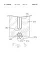
- FIG. 5a further alternate embodiment is shown having the diode 370 mounted as a "flip chip" or on the surface of the substrate 320 opposite the surface which is adjacent the focusing element 360 so that the emission point is abutting the substrate and transmits therethrough.
- the diodemay include, but is not limited to, an LED, a VCSEL, a laser diode or a photodiode.
- the substrate 320may have its electronics connected via flexible circuit member 372 to external components.
- the substrate 320is preferably formed of a material which is optically transmissive and allows for the transmission of lightwaves of up to 780-1350 nanometers such as silicon or transparent glass.
- the embodiment of FIG. 5also allows for passive alignment similar to the embodiment of FIG. 4 in that the substrate is positioned within aperture 355 so that the prepositioned diode 370 is aligned on the optical axis along with the focusing element 361 and the bore 351.
Landscapes
- Physics & Mathematics (AREA)
- General Physics & Mathematics (AREA)
- Optics & Photonics (AREA)
- Optical Couplings Of Light Guides (AREA)
- Led Device Packages (AREA)
Abstract
Description
Claims (43)
Priority Applications (5)
| Application Number | Priority Date | Filing Date | Title |
|---|---|---|---|
| US08/588,445US5812717A (en) | 1996-01-18 | 1996-01-18 | Optical package with alignment means and method of assembling an optical package |
| US08/862,899US5815623A (en) | 1996-01-18 | 1997-05-23 | Optical package with alignment means and method of assembling an optical package |
| US09/095,243US6071017A (en) | 1996-01-18 | 1998-06-10 | Optical package with alignment means and method of assembling an optical package |
| US09/122,460US6550983B1 (en) | 1996-01-18 | 1998-07-24 | Optical package with alignment means and method of assembling an optical package |
| US09/309,654US6283644B1 (en) | 1996-01-18 | 1999-05-10 | Optical package with alignment means and method of assembling an optical package |
Applications Claiming Priority (1)
| Application Number | Priority Date | Filing Date | Title |
|---|---|---|---|
| US08/588,445US5812717A (en) | 1996-01-18 | 1996-01-18 | Optical package with alignment means and method of assembling an optical package |
Related Child Applications (1)
| Application Number | Title | Priority Date | Filing Date |
|---|---|---|---|
| US08/862,899Continuation-In-PartUS5815623A (en) | 1996-01-18 | 1997-05-23 | Optical package with alignment means and method of assembling an optical package |
Publications (1)
| Publication Number | Publication Date |
|---|---|
| US5812717Atrue US5812717A (en) | 1998-09-22 |
Family
ID=24353882
Family Applications (1)
| Application Number | Title | Priority Date | Filing Date |
|---|---|---|---|
| US08/588,445Expired - LifetimeUS5812717A (en) | 1996-01-18 | 1996-01-18 | Optical package with alignment means and method of assembling an optical package |
Country Status (1)
| Country | Link |
|---|---|
| US (1) | US5812717A (en) |
Cited By (51)
| Publication number | Priority date | Publication date | Assignee | Title |
|---|---|---|---|---|
| US5971628A (en)* | 1996-10-23 | 1999-10-26 | Jds Uniphase Corporation | Holder for optoelectronic device having connection pins bent toward a connection means |
| US6061493A (en)* | 1998-09-01 | 2000-05-09 | Methode Electronics, Inc. | Optical subassembly with attenuating plug |
| US6071017A (en)* | 1996-01-18 | 2000-06-06 | Methode Electronics, Inc. | Optical package with alignment means and method of assembling an optical package |
| US6213651B1 (en) | 1999-05-26 | 2001-04-10 | E20 Communications, Inc. | Method and apparatus for vertical board construction of fiber optic transmitters, receivers and transceivers |
| US6283644B1 (en)* | 1996-01-18 | 2001-09-04 | Stratos Lightwave, Inc. | Optical package with alignment means and method of assembling an optical package |
| US20010048793A1 (en)* | 1999-05-27 | 2001-12-06 | Edwin Dair | Method and apparatus for multiboard fiber optic modules and fiber optic module arrays |
| WO2002012942A1 (en)* | 2000-08-07 | 2002-02-14 | Stratos Lightwave, Inc. | Modular high density multiple optical transmitter/receiver array |
| US20020028048A1 (en)* | 1999-05-27 | 2002-03-07 | Edwin Dair | Method and apparatus for multiboard fiber optic modules and fiber optic module arrays |
| US20020030872A1 (en)* | 1999-05-27 | 2002-03-14 | Edwin Dair | Method and apparatus for multiboard fiber optic modules and fiber optic module arrays |
| US20020033979A1 (en)* | 1999-05-27 | 2002-03-21 | Edwin Dair | Method and apparatus for multiboard fiber optic modules and fiber optic module arrays |
| US6550983B1 (en)* | 1996-01-18 | 2003-04-22 | Stratos Lightwave Llc | Optical package with alignment means and method of assembling an optical package |
| US6550127B1 (en)* | 1999-03-19 | 2003-04-22 | Infineon Technologies Aktiengesellschaft | Device for holding a part and application of the device |
| US6583902B1 (en) | 1999-12-09 | 2003-06-24 | Alvesta, Inc. | Modular fiber-optic transceiver |
| US6632030B2 (en) | 1999-05-27 | 2003-10-14 | E20 Communications, Inc. | Light bending optical block for fiber optic modules |
| US20030234403A1 (en)* | 2002-06-20 | 2003-12-25 | Chung-Shin Mou | Optical package structure |
| US20040069997A1 (en)* | 1999-05-27 | 2004-04-15 | Edwin Dair | Method and apparatus for multiboard fiber optic modules and fiber optic module arrays |
| US6741778B1 (en)* | 2000-05-23 | 2004-05-25 | International Business Machines Corporation | Optical device with chip level precision alignment |
| US6799902B2 (en) | 2000-12-26 | 2004-10-05 | Emcore Corporation | Optoelectronic mounting structure |
| US6863444B2 (en) | 2000-12-26 | 2005-03-08 | Emcore Corporation | Housing and mounting structure |
| US6863453B2 (en) | 2003-01-28 | 2005-03-08 | Emcore Corporation | Method and apparatus for parallel optical transceiver module assembly |
| US6867377B2 (en) | 2000-12-26 | 2005-03-15 | Emcore Corporation | Apparatus and method of using flexible printed circuit board in optical transceiver device |
| US6873800B1 (en) | 1999-05-26 | 2005-03-29 | Jds Uniphase Corporation | Hot pluggable optical transceiver in a small form pluggable package |
| US6901221B1 (en) | 1999-05-27 | 2005-05-31 | Jds Uniphase Corporation | Method and apparatus for improved optical elements for vertical PCB fiber optic modules |
| US6905260B2 (en) | 2000-12-26 | 2005-06-14 | Emcore Corporation | Method and apparatus for coupling optical elements to optoelectronic devices for manufacturing optical transceiver modules |
| US20050141820A1 (en)* | 2003-10-01 | 2005-06-30 | Tyco Electronics Corporation | Optoelectric package |
| US20050239227A1 (en)* | 2002-08-30 | 2005-10-27 | Gelcore, Llc | Light emitting diode component |
| US20050280888A1 (en)* | 2002-05-03 | 2005-12-22 | Jing-Jong Pan | Erbium-doped fiber amplifier and integrated circuit module components |
| US7002131B1 (en) | 2003-01-24 | 2006-02-21 | Jds Uniphase Corporation | Methods, systems and apparatus for measuring average received optical power |
| US7004644B1 (en) | 1999-06-29 | 2006-02-28 | Finisar Corporation | Hermetic chip-scale package for photonic devices |
| US7013088B1 (en) | 1999-05-26 | 2006-03-14 | Jds Uniphase Corporation | Method and apparatus for parallel optical interconnection of fiber optic transmitters, receivers and transceivers |
| US7021836B2 (en) | 2000-12-26 | 2006-04-04 | Emcore Corporation | Attenuator and conditioner |
| US20060097245A1 (en)* | 2002-08-30 | 2006-05-11 | Aanegola Srinath K | Light emitting diode component |
| US7116912B2 (en) | 1999-05-27 | 2006-10-03 | Jds Uniphase Corporation | Method and apparatus for pluggable fiber optic modules |
| US20060278821A1 (en)* | 1998-11-25 | 2006-12-14 | Rohm And Haas Electronic Materials Llc | Optoelectronic component |
| US20070063125A1 (en)* | 2005-09-20 | 2007-03-22 | Downing John P Jr | Semiconductor light source with optical feedback |
| US20070081310A1 (en)* | 2005-09-23 | 2007-04-12 | Kowalkowski Anthony S | Cageless, pluggable optoelectronic device |
| US7215883B1 (en) | 2003-01-24 | 2007-05-08 | Jds Uniphase Corporation | Methods for determining the performance, status, and advanced failure of optical communication channels |
| US7329056B2 (en) | 2003-09-15 | 2008-02-12 | Rohm And Haas Electronic Materials Llc | Device package and methods for the fabrication and testing thereof |
| US20080050072A1 (en)* | 2006-08-23 | 2008-02-28 | Durrant Richard S E | Expanded beam, single fiber, fiber optic connector |
| US20080054280A1 (en)* | 2006-09-06 | 2008-03-06 | Gelcore Llc | Light emitting packages and methods of making same |
| US20080170375A1 (en)* | 2007-01-16 | 2008-07-17 | John Jablonski | Optoelectronic device in combination with a push-in cage |
| US20110311182A1 (en)* | 2010-06-16 | 2011-12-22 | Avago Technologies Fiber Ip (Singapore) Pte. Ltd. | Opto-electronic alignment system and method |
| US20120104240A1 (en)* | 2010-10-27 | 2012-05-03 | Avago Technologies Fiber Ip (Singapore) Pte. Ltd. | Fiber optic transceiver (fot) module having a molded cover in which an optical beam transformer is integrally formed |
| US8502452B2 (en) | 2010-07-28 | 2013-08-06 | Usl Technologies, Llc | High-stability light source system and method of manufacturing |
| US20140049965A1 (en)* | 2002-08-30 | 2014-02-20 | GE Lighting Solutions, LLC | Light emitting diode component |
| US20140126863A1 (en)* | 2012-11-07 | 2014-05-08 | Silicon Image, Inc. | Methods and apparatuses to provide an electro-optical alignment |
| US8905648B2 (en) | 2011-06-29 | 2014-12-09 | Cinch Connectivity Solutions, Inc. | Expanded beam fiber optic connector |
| US9841175B2 (en) | 2012-05-04 | 2017-12-12 | GE Lighting Solutions, LLC | Optics system for solid state lighting apparatus |
| US9951938B2 (en) | 2009-10-02 | 2018-04-24 | GE Lighting Solutions, LLC | LED lamp |
| US10319654B1 (en) | 2017-12-01 | 2019-06-11 | Cubic Corporation | Integrated chip scale packages |
| CN110959130A (en)* | 2017-07-28 | 2020-04-03 | 弗劳恩霍夫应用研究促进协会 | MEMS mirror assembly and method for making MEMS mirror assembly |
Citations (8)
| Publication number | Priority date | Publication date | Assignee | Title |
|---|---|---|---|---|
| US4979791A (en)* | 1989-12-08 | 1990-12-25 | Amp Incorporated | Laser diode connector assembly |
| US5243681A (en)* | 1992-04-13 | 1993-09-07 | Amp Incorporated | Aperture disk attenuator for laser diode connector |
| US5257336A (en)* | 1992-08-21 | 1993-10-26 | At&T Bell Laboratories | Optical subassembly with passive optical alignment |
| US5259053A (en)* | 1992-06-29 | 1993-11-02 | The Whitaker Corporation | Discrete optical receptacle assembly with alignment feature |
| US5337398A (en)* | 1992-11-30 | 1994-08-09 | At&T Bell Laboratories | Single in-line optical package |
| US5357593A (en)* | 1993-10-12 | 1994-10-18 | Alliedsignal Inc. | Method of attaching optical fibers to opto-electronic integrated circuits on silicon substrates |
| USRE34790E (en)* | 1988-07-13 | 1994-11-15 | Bt&D Technologies Limited | Optical components |
| US5452389A (en)* | 1993-04-16 | 1995-09-19 | Sumitomo Electric Industries, Ltd. | Semiconductor element module |
- 1996
- 1996-01-18USUS08/588,445patent/US5812717A/ennot_activeExpired - Lifetime
Patent Citations (8)
| Publication number | Priority date | Publication date | Assignee | Title |
|---|---|---|---|---|
| USRE34790E (en)* | 1988-07-13 | 1994-11-15 | Bt&D Technologies Limited | Optical components |
| US4979791A (en)* | 1989-12-08 | 1990-12-25 | Amp Incorporated | Laser diode connector assembly |
| US5243681A (en)* | 1992-04-13 | 1993-09-07 | Amp Incorporated | Aperture disk attenuator for laser diode connector |
| US5259053A (en)* | 1992-06-29 | 1993-11-02 | The Whitaker Corporation | Discrete optical receptacle assembly with alignment feature |
| US5257336A (en)* | 1992-08-21 | 1993-10-26 | At&T Bell Laboratories | Optical subassembly with passive optical alignment |
| US5337398A (en)* | 1992-11-30 | 1994-08-09 | At&T Bell Laboratories | Single in-line optical package |
| US5452389A (en)* | 1993-04-16 | 1995-09-19 | Sumitomo Electric Industries, Ltd. | Semiconductor element module |
| US5357593A (en)* | 1993-10-12 | 1994-10-18 | Alliedsignal Inc. | Method of attaching optical fibers to opto-electronic integrated circuits on silicon substrates |
Cited By (86)
| Publication number | Priority date | Publication date | Assignee | Title |
|---|---|---|---|---|
| US6550983B1 (en)* | 1996-01-18 | 2003-04-22 | Stratos Lightwave Llc | Optical package with alignment means and method of assembling an optical package |
| US6071017A (en)* | 1996-01-18 | 2000-06-06 | Methode Electronics, Inc. | Optical package with alignment means and method of assembling an optical package |
| US6283644B1 (en)* | 1996-01-18 | 2001-09-04 | Stratos Lightwave, Inc. | Optical package with alignment means and method of assembling an optical package |
| US5971628A (en)* | 1996-10-23 | 1999-10-26 | Jds Uniphase Corporation | Holder for optoelectronic device having connection pins bent toward a connection means |
| US6061493A (en)* | 1998-09-01 | 2000-05-09 | Methode Electronics, Inc. | Optical subassembly with attenuating plug |
| US7291833B2 (en) | 1998-11-25 | 2007-11-06 | Rohm And Haas Electronic Materials Llc | Optoelectronic component |
| US20060278821A1 (en)* | 1998-11-25 | 2006-12-14 | Rohm And Haas Electronic Materials Llc | Optoelectronic component |
| US6550127B1 (en)* | 1999-03-19 | 2003-04-22 | Infineon Technologies Aktiengesellschaft | Device for holding a part and application of the device |
| US6840686B2 (en) | 1999-05-26 | 2005-01-11 | Jds Uniphase Corporation | Method and apparatus for vertical board construction of fiber optic transmitters, receivers and transceivers |
| US7013088B1 (en) | 1999-05-26 | 2006-03-14 | Jds Uniphase Corporation | Method and apparatus for parallel optical interconnection of fiber optic transmitters, receivers and transceivers |
| US6873800B1 (en) | 1999-05-26 | 2005-03-29 | Jds Uniphase Corporation | Hot pluggable optical transceiver in a small form pluggable package |
| US6213651B1 (en) | 1999-05-26 | 2001-04-10 | E20 Communications, Inc. | Method and apparatus for vertical board construction of fiber optic transmitters, receivers and transceivers |
| US20040069997A1 (en)* | 1999-05-27 | 2004-04-15 | Edwin Dair | Method and apparatus for multiboard fiber optic modules and fiber optic module arrays |
| US6952532B2 (en) | 1999-05-27 | 2005-10-04 | Jds Uniphase Corporation | Method and apparatus for multiboard fiber optic modules and fiber optic module arrays |
| US6632030B2 (en) | 1999-05-27 | 2003-10-14 | E20 Communications, Inc. | Light bending optical block for fiber optic modules |
| USRE41147E1 (en)* | 1999-05-27 | 2010-02-23 | Jds Uniphase Corporation | Method and apparatus for pluggable fiber optic modules |
| US20020030872A1 (en)* | 1999-05-27 | 2002-03-14 | Edwin Dair | Method and apparatus for multiboard fiber optic modules and fiber optic module arrays |
| US20020033979A1 (en)* | 1999-05-27 | 2002-03-21 | Edwin Dair | Method and apparatus for multiboard fiber optic modules and fiber optic module arrays |
| US6901221B1 (en) | 1999-05-27 | 2005-05-31 | Jds Uniphase Corporation | Method and apparatus for improved optical elements for vertical PCB fiber optic modules |
| US20020028048A1 (en)* | 1999-05-27 | 2002-03-07 | Edwin Dair | Method and apparatus for multiboard fiber optic modules and fiber optic module arrays |
| US20010048793A1 (en)* | 1999-05-27 | 2001-12-06 | Edwin Dair | Method and apparatus for multiboard fiber optic modules and fiber optic module arrays |
| US7116912B2 (en) | 1999-05-27 | 2006-10-03 | Jds Uniphase Corporation | Method and apparatus for pluggable fiber optic modules |
| US7004644B1 (en) | 1999-06-29 | 2006-02-28 | Finisar Corporation | Hermetic chip-scale package for photonic devices |
| US6583902B1 (en) | 1999-12-09 | 2003-06-24 | Alvesta, Inc. | Modular fiber-optic transceiver |
| US6741778B1 (en)* | 2000-05-23 | 2004-05-25 | International Business Machines Corporation | Optical device with chip level precision alignment |
| US6416238B1 (en)* | 2000-08-07 | 2002-07-09 | Stratos Lightwave, Inc. | Modular high density multiple optical transmitter/receiver array |
| WO2002012942A1 (en)* | 2000-08-07 | 2002-02-14 | Stratos Lightwave, Inc. | Modular high density multiple optical transmitter/receiver array |
| US6867377B2 (en) | 2000-12-26 | 2005-03-15 | Emcore Corporation | Apparatus and method of using flexible printed circuit board in optical transceiver device |
| US6799902B2 (en) | 2000-12-26 | 2004-10-05 | Emcore Corporation | Optoelectronic mounting structure |
| US6905260B2 (en) | 2000-12-26 | 2005-06-14 | Emcore Corporation | Method and apparatus for coupling optical elements to optoelectronic devices for manufacturing optical transceiver modules |
| US7021836B2 (en) | 2000-12-26 | 2006-04-04 | Emcore Corporation | Attenuator and conditioner |
| US6863444B2 (en) | 2000-12-26 | 2005-03-08 | Emcore Corporation | Housing and mounting structure |
| US7044660B2 (en)* | 2002-05-03 | 2006-05-16 | Lightwaves 2020, Inc. | Erbium-doped fiber amplifier and integrated circuit module components |
| US20050280888A1 (en)* | 2002-05-03 | 2005-12-22 | Jing-Jong Pan | Erbium-doped fiber amplifier and integrated circuit module components |
| US20030234403A1 (en)* | 2002-06-20 | 2003-12-25 | Chung-Shin Mou | Optical package structure |
| US8362695B2 (en) | 2002-08-30 | 2013-01-29 | GE Lighting Solutions, LLC | Light emitting diode component |
| US20050239227A1 (en)* | 2002-08-30 | 2005-10-27 | Gelcore, Llc | Light emitting diode component |
| US10340424B2 (en)* | 2002-08-30 | 2019-07-02 | GE Lighting Solutions, LLC | Light emitting diode component |
| US20060097245A1 (en)* | 2002-08-30 | 2006-05-11 | Aanegola Srinath K | Light emitting diode component |
| US20110001422A1 (en)* | 2002-08-30 | 2011-01-06 | Lumination Llc | Light emitting diode component |
| US7800121B2 (en) | 2002-08-30 | 2010-09-21 | Lumination Llc | Light emitting diode component |
| US20140049965A1 (en)* | 2002-08-30 | 2014-02-20 | GE Lighting Solutions, LLC | Light emitting diode component |
| US7224000B2 (en)* | 2002-08-30 | 2007-05-29 | Lumination, Llc | Light emitting diode component |
| US8436380B2 (en) | 2002-08-30 | 2013-05-07 | GE Lighting Solutions, LLC | Light emitting diode component |
| US7215883B1 (en) | 2003-01-24 | 2007-05-08 | Jds Uniphase Corporation | Methods for determining the performance, status, and advanced failure of optical communication channels |
| US7002131B1 (en) | 2003-01-24 | 2006-02-21 | Jds Uniphase Corporation | Methods, systems and apparatus for measuring average received optical power |
| US6863453B2 (en) | 2003-01-28 | 2005-03-08 | Emcore Corporation | Method and apparatus for parallel optical transceiver module assembly |
| US8703603B2 (en) | 2003-09-15 | 2014-04-22 | Nuvotronics, Llc | Device package and methods for the fabrication and testing thereof |
| US9647420B2 (en) | 2003-09-15 | 2017-05-09 | Nuvotronics, Inc. | Package and methods for the fabrication and testing thereof |
| US9410799B2 (en) | 2003-09-15 | 2016-08-09 | Nuvotronics, Inc. | Device package and methods for the fabrication and testing thereof |
| US8993450B2 (en) | 2003-09-15 | 2015-03-31 | Nuvotronics, Llc | Device package and methods for the fabrication and testing thereof |
| US9817199B2 (en) | 2003-09-15 | 2017-11-14 | Nuvotronics, Inc | Device package and methods for the fabrication and testing thereof |
| US7329056B2 (en) | 2003-09-15 | 2008-02-12 | Rohm And Haas Electronic Materials Llc | Device package and methods for the fabrication and testing thereof |
| US7888793B2 (en) | 2003-09-15 | 2011-02-15 | Nuvotronics, Llc | Device package and methods for the fabrication and testing thereof |
| US20110079893A1 (en)* | 2003-09-15 | 2011-04-07 | Sherrer David W | Device package and methods for the fabrication and testing thereof |
| US20050141820A1 (en)* | 2003-10-01 | 2005-06-30 | Tyco Electronics Corporation | Optoelectric package |
| AU2005239406B2 (en)* | 2004-04-26 | 2011-10-06 | Gelcore Llc | Light emitting diode component |
| WO2005106926A3 (en)* | 2004-04-26 | 2006-06-01 | Gelcore Llc | Light emitting diode component |
| US7767947B2 (en) | 2005-09-20 | 2010-08-03 | Downing Jr John P | Semiconductor light source with optical feedback |
| US20070063125A1 (en)* | 2005-09-20 | 2007-03-22 | Downing John P Jr | Semiconductor light source with optical feedback |
| US20070081310A1 (en)* | 2005-09-23 | 2007-04-12 | Kowalkowski Anthony S | Cageless, pluggable optoelectronic device |
| US7227745B2 (en) | 2005-09-23 | 2007-06-05 | Stratos International, Inc. | Cageless, pluggable optoelectronic device |
| US20080279509A1 (en)* | 2006-08-23 | 2008-11-13 | Stratos International, Inc. | Expanded beam, single fiber, fiber optic connector |
| US20080050072A1 (en)* | 2006-08-23 | 2008-02-28 | Durrant Richard S E | Expanded beam, single fiber, fiber optic connector |
| US8244084B2 (en)* | 2006-08-23 | 2012-08-14 | Stratos International, Inc. | Expanded beam, single fiber, fiber optic connector |
| US20100166372A1 (en)* | 2006-08-23 | 2010-07-01 | Stratos International, Inc. | Expanded beam, single fiber, fiber optic connector |
| US7460750B2 (en)* | 2006-08-23 | 2008-12-02 | Stratos International, Inc. | Expanded beam, single fiber, fiber optic connector |
| US20080054280A1 (en)* | 2006-09-06 | 2008-03-06 | Gelcore Llc | Light emitting packages and methods of making same |
| US7842960B2 (en) | 2006-09-06 | 2010-11-30 | Lumination Llc | Light emitting packages and methods of making same |
| US20080170375A1 (en)* | 2007-01-16 | 2008-07-17 | John Jablonski | Optoelectronic device in combination with a push-in cage |
| US7419313B2 (en) | 2007-01-16 | 2008-09-02 | Stratos International, Inc. | Optoelectronic device in combination with a push-in cage |
| US9951938B2 (en) | 2009-10-02 | 2018-04-24 | GE Lighting Solutions, LLC | LED lamp |
| US8260097B2 (en)* | 2010-06-16 | 2012-09-04 | Avago Technologies Fiber Ip (Singapore) Pte. Ltd | Opto-electronic alignment system and method |
| US20110311182A1 (en)* | 2010-06-16 | 2011-12-22 | Avago Technologies Fiber Ip (Singapore) Pte. Ltd. | Opto-electronic alignment system and method |
| US8502452B2 (en) | 2010-07-28 | 2013-08-06 | Usl Technologies, Llc | High-stability light source system and method of manufacturing |
| US20120104240A1 (en)* | 2010-10-27 | 2012-05-03 | Avago Technologies Fiber Ip (Singapore) Pte. Ltd. | Fiber optic transceiver (fot) module having a molded cover in which an optical beam transformer is integrally formed |
| US8581173B2 (en)* | 2010-10-27 | 2013-11-12 | Avago Technologies General Ip (Singapore) Pte. Ltd. | Fiber optic transceiver module having a molded cover in which an optical beam transformer made of an elastomer is integrally formed |
| US8905648B2 (en) | 2011-06-29 | 2014-12-09 | Cinch Connectivity Solutions, Inc. | Expanded beam fiber optic connector |
| US10139095B2 (en) | 2012-05-04 | 2018-11-27 | GE Lighting Solutions, LLC | Reflector and lamp comprised thereof |
| US9841175B2 (en) | 2012-05-04 | 2017-12-12 | GE Lighting Solutions, LLC | Optics system for solid state lighting apparatus |
| US9497860B2 (en)* | 2012-11-07 | 2016-11-15 | Lattice Semiconductor Corporation | Methods and Apparatuses to provide an electro-optical alignment |
| US20140126863A1 (en)* | 2012-11-07 | 2014-05-08 | Silicon Image, Inc. | Methods and apparatuses to provide an electro-optical alignment |
| CN110959130A (en)* | 2017-07-28 | 2020-04-03 | 弗劳恩霍夫应用研究促进协会 | MEMS mirror assembly and method for making MEMS mirror assembly |
| CN110959130B (en)* | 2017-07-28 | 2022-08-16 | 弗劳恩霍夫应用研究促进协会 | MEMS mirror assembly and method for manufacturing a MEMS mirror assembly |
| US10319654B1 (en) | 2017-12-01 | 2019-06-11 | Cubic Corporation | Integrated chip scale packages |
| US10553511B2 (en) | 2017-12-01 | 2020-02-04 | Cubic Corporation | Integrated chip scale packages |
Similar Documents
| Publication | Publication Date | Title |
|---|---|---|
| US5812717A (en) | Optical package with alignment means and method of assembling an optical package | |
| US5815623A (en) | Optical package with alignment means and method of assembling an optical package | |
| US6071017A (en) | Optical package with alignment means and method of assembling an optical package | |
| US6550983B1 (en) | Optical package with alignment means and method of assembling an optical package | |
| US6283644B1 (en) | Optical package with alignment means and method of assembling an optical package | |
| US5737467A (en) | Resin molded optical assembly | |
| EP0982610B1 (en) | Optical subassembly for use in fiber optic data transmission and reception | |
| US5896481A (en) | Optical subassembly with a groove for aligning an optical device with an optical fiber | |
| US6795461B1 (en) | Optoelectric module | |
| US7050678B1 (en) | Optical module, optical element attachment method, and receptacle-fitted optical module | |
| US5937124A (en) | Package for an optoelectronic device | |
| US20040101020A1 (en) | Packaging and passive alignment of light source to single mode fiber using microlens and precision ferrule | |
| US20060257082A1 (en) | Connection of optical waveguides to optical devices | |
| EP1729159A1 (en) | Optical assemblies | |
| WO2004042320A1 (en) | Planar and wafer level packaging of semiconductor lasers and photo detectors for transmitter optical sub-assemblies | |
| US5029968A (en) | Optoelectronic hybrid package assembly including integral, self-aligned fiber optic connector | |
| CN101303439A (en) | Optical component and method of forming the same | |
| US6663296B1 (en) | Optoelectric module | |
| JP2005173534A (en) | Ferrule block and optical module using the same | |
| US7410306B2 (en) | Opto-electronic device for optical fibre applications | |
| US6371665B1 (en) | Plastic packaged optoelectronic device | |
| US7093986B2 (en) | Low cost optical module | |
| US6999494B2 (en) | Packaging and passive alignment of microlens and molded receptacle | |
| US6999644B1 (en) | Discrete optoelectric package | |
| US6893170B1 (en) | Optical/electrical module |
Legal Events
| Date | Code | Title | Description |
|---|---|---|---|
| AS | Assignment | Owner name:METHODE ELECTRONICS, INC., ILLINOIS Free format text:ASSIGNMENT OF ASSIGNORS INTEREST;ASSIGNOR:GILLILAND, PATRICK B.;REEL/FRAME:007916/0238 Effective date:19960115 | |
| STCF | Information on status: patent grant | Free format text:PATENTED CASE | |
| AS | Assignment | Owner name:STRATOS LIGHTWAVE LLC, ILLINOIS Free format text:ASSIGNMENT OF ASSIGNORS INTEREST;ASSIGNORS:METHODE ELECTRONICS, INC.;STRATOS LIGHTWAVE LLC;REEL/FRAME:010949/0722;SIGNING DATES FROM 20000605 TO 20000621 | |
| FPAY | Fee payment | Year of fee payment:4 | |
| FPAY | Fee payment | Year of fee payment:8 | |
| AS | Assignment | Owner name:STRATOS LIGHTWAVE, INC., ILLINOIS Free format text:ASSIGNMENT OF ASSIGNORS INTEREST;ASSIGNOR:STRATOS LIGHTWAVE LLC;REEL/FRAME:022542/0100 Effective date:20000621 Owner name:STRATOS INTERNATIONAL, INC., ILLINOIS Free format text:CHANGE OF NAME;ASSIGNOR:STRATOS LIGHTWAVE, INC.;REEL/FRAME:022542/0180 Effective date:20031121 | |
| REMI | Maintenance fee reminder mailed | ||
| FPAY | Fee payment | Year of fee payment:12 | |
| SULP | Surcharge for late payment | Year of fee payment:11 | |
| AS | Assignment | Owner name:KEYBANK NATIONAL ASSOCIATION, AS ADMINISTRATIVE AG Free format text:INTELLECTUAL PROPERTY SECURITY AGREEMENT;ASSIGNOR:STRATOS INTERNATIONAL, LLC;REEL/FRAME:033429/0049 Effective date:20140725 |