US5812268A - Grid array inspection system and method - Google Patents
Grid array inspection system and methodDownload PDFInfo
- Publication number
- US5812268A US5812268AUS08/850,286US85028697AUS5812268AUS 5812268 AUS5812268 AUS 5812268AUS 85028697 AUS85028697 AUS 85028697AUS 5812268 AUS5812268 AUS 5812268A
- Authority
- US
- United States
- Prior art keywords
- grid
- ball
- pin
- grid array
- height
- Prior art date
- Legal status (The legal status is an assumption and is not a legal conclusion. Google has not performed a legal analysis and makes no representation as to the accuracy of the status listed.)
- Expired - Lifetime
Links
- 238000007689inspectionMethods0.000titleclaimsabstractdescription34
- 238000000034methodMethods0.000titleclaimsdescription43
- 238000012545processingMethods0.000claimsabstractdescription6
- 230000008569processEffects0.000claimsdescription7
- 238000003491arrayMethods0.000abstractdescription20
- 238000005259measurementMethods0.000abstractdescription17
- 239000000969carrierSubstances0.000abstractdescription4
- 230000000712assemblyEffects0.000abstractdescription3
- 238000000429assemblyMethods0.000abstractdescription3
- 150000001875compoundsChemical class0.000description30
- 239000004065semiconductorSubstances0.000description11
- 229910000679solderInorganic materials0.000description8
- 230000007704transitionEffects0.000description7
- 238000004519manufacturing processMethods0.000description6
- 238000010586diagramMethods0.000description4
- 230000007547defectEffects0.000description3
- 238000001514detection methodMethods0.000description3
- 230000000694effectsEffects0.000description3
- 238000012360testing methodMethods0.000description3
- 230000006978adaptationEffects0.000description2
- 230000009977dual effectEffects0.000description2
- 238000001914filtrationMethods0.000description2
- 238000003384imaging methodMethods0.000description2
- 230000001537neural effectEffects0.000description2
- 210000002569neuronAnatomy0.000description2
- 230000010287polarizationEffects0.000description2
- 230000009467reductionEffects0.000description2
- 239000004020conductorSubstances0.000description1
- 238000010276constructionMethods0.000description1
- 238000013480data collectionMethods0.000description1
- 230000001419dependent effectEffects0.000description1
- 238000013461designMethods0.000description1
- 238000011161developmentMethods0.000description1
- 230000006870functionEffects0.000description1
- 239000010438graniteSubstances0.000description1
- 230000007246mechanismEffects0.000description1
- 238000012986modificationMethods0.000description1
- 230000004048modificationEffects0.000description1
- 238000005457optimizationMethods0.000description1
- 230000008447perceptionEffects0.000description1
- 238000003908quality control methodMethods0.000description1
- 230000004044responseEffects0.000description1
- 239000002356single layerSubstances0.000description1
- 239000007787solidSubstances0.000description1
- 230000000007visual effectEffects0.000description1
Images


Classifications
- G—PHYSICS
- G01—MEASURING; TESTING
- G01N—INVESTIGATING OR ANALYSING MATERIALS BY DETERMINING THEIR CHEMICAL OR PHYSICAL PROPERTIES
- G01N21/00—Investigating or analysing materials by the use of optical means, i.e. using sub-millimetre waves, infrared, visible or ultraviolet light
- G01N21/84—Systems specially adapted for particular applications
- G01N21/88—Investigating the presence of flaws or contamination
- G01N21/95—Investigating the presence of flaws or contamination characterised by the material or shape of the object to be examined
- G01N21/956—Inspecting patterns on the surface of objects
- G—PHYSICS
- G01—MEASURING; TESTING
- G01N—INVESTIGATING OR ANALYSING MATERIALS BY DETERMINING THEIR CHEMICAL OR PHYSICAL PROPERTIES
- G01N21/00—Investigating or analysing materials by the use of optical means, i.e. using sub-millimetre waves, infrared, visible or ultraviolet light
- G01N21/84—Systems specially adapted for particular applications
- G01N21/88—Investigating the presence of flaws or contamination
Definitions
- This inventionrelates to an automatic grid array inspection system, and more particularly, to a automatic, non-contact inspection system for measuring the dimensional and geometric characteristics of semiconductor device packages.
- connections that contact the surface of the boardmust be very close to each other (fine pitch) and very close to the board thereby requiring very narrow and mechanically fragile leads.
- the length and geometry of the leadis critical as all connections must make contact with the wiring board pads without damage to the semiconductor, shorting or other connection defects. If one or more leads are too long then one or more other leads may not be able to provide a reliable contact to the board pad. If one or more leads are displaced or bent they may miss the pad or short circuit to an adjacent pad. It is critical therefore that the X and Y positions as well as the height and geometry of each connection is within the manufacturing tolerance of the semiconductor package design.
- pin grid arraysmay exhibit defects not previously encountered in other package types (such as the compound bend of a pin).
- the inspection methodmust be high speed in order to keep the cost of inspection to a minimum. Since the semiconductors have many interconnects (often above 200 and up to 400) and are physically large in area (up to 3.0 inches per side) the sensors, architecture and algorithms must support this requirement.
- Previous systemsprovided measurement equipment for determining the dimensional lead integrity for semiconductor packages whose leads were on the outer periphery of the package, such as quad flat packs (QFP's) and single outline integrated circuit's.
- Visual imagingprovided data used to identify broken leads, lack of leads, bent leads, and the angle of leads.
- Point laser triangulation systemsprovide adequate height information however, because of their limited measurement area and rates are much too slow for production volume testing.
- the systemmust be cost effective in determining the two-dimensional positioning of the balls and pins on the grid, in determining the height of each, in detecting bent pins, and in measuring coplanarity at rates for 100% inspection. Further, the system must perform the inspection with high speed and high accuracy.
- the present inventiondiscloses a high speed, high accuracy, three-dimensional inspection system for ball and pin grid assemblies.
- a high speed, high resolution, three-dimensional scanner and imaging systemis used to gather height information.
- the collected datais then analyzed to yield height and position measurements along with overall packaged dimensions.
- the three-dimensional scanneronly scans in one dimension and therefore must be continually repositioned (scanned) to provide full coverage of the grid arrays.
- a metrology-grade stage unitis provided to position the laser.
- a motion control systemdirects the movement of the metrology stage in response to commands received from a computer.
- the field of view of the laser scanner systemmay be matched to the dimensions of the package being inspected to provide inspection capabilities for the entire package.
- the array to be scannedmay be placed upon an inspection platform either manually or automatically.
- arraysare loaded onto a fixture by hand and the image processing hardware is activated.
- the fixtureconsists of a plate with a cavity the size of the grid array package being inspected. The size of the cavity can be adjusted to fit different size grid arrays.
- An automatic pick and place systemmay be used instead to load grid array packages on the fixture above the stage.
- the partscan be presented in single trays, tray stackers, tubes or other carriers.
- the automatic systemhas the capability of repackaging the parts as well. Thus, after inspection, parts can be placed back in the tray tubes and can be sorted according to pass or fail.
- the inspection modulewas designed small so as to allow it to be incorporated in the in-line manufacture and test of the components.
- the grid array inspection systemcan also measure element spacing, lead height, coplanarity, standoff, grid pitch, ball diameter, ball position, and package warp.
- the inventionalso includes a high speed algorithm means for determining, with a high degree of confidence, the presence of compound bends, a defect prevalent and unique to the pin grid array package.
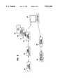
- FIG. 1is a system diagram of the grid array inspection system
- FIG. 2is a block diagram of the grid array inspection system
- FIG. 3is a block diagram of the dual detector utilized in one embodiment of the invention.
- FIG. 4is plan view of a pin grid array package
- FIGS. 5A-5Cillustrate the method used by the grid array inspection system to locate a pin
- FIGS. 6A and 6Billustrate a side view and a plan view, respectively, of a pin experiencing a compound bend
- FIG. 7illustrates a first and second method of locating the position of a pin experiencing a compound bend
- FIG. 8illustrates a third and fourth method for locating the position of a pin experiencing a compound bend
- FIG. 9is a plot of the radial profile resulting from the third method for locating the position of a pin experiencing a compound bend
- FIG. 10illustrates the tangential profile method for locating the position of a compound bend
- FIG. 11is a plot of the dark to light and light to dark transitions obtain from the radial profile method
- FIG. 12illustrates the method for finding the location of a ball grid
- FIG. 13shows a profile for a ball and an aligned and unaligned window.
- the present inventionprovides a grid array inspection system. Inspection system identifies height and position data pertaining to both ball grid arrays and pin grid arrays.
- FIG. 1illustrates an exemplary system 10 according to the present invention.
- the grid array 12 to be inspectedis placed on a inspection platform 14 which is positioned over a scanning laser 16. Handling of the grid arrays 12 can be performed manually or automatically. The manual method involves merely placing the grid array 12 by hand in to a holding fixture 18.
- the fixture 18consists of a plate with a cavity the size of the grid array package 12 being inspected. The size of the cavity can be adjusted to fit different size grid arrays 12.
- An automatic systemuses a pick and place module to load the grid array packages 12 on the inspection platform 14.
- the grid array packages 12can be presented in single trays, tray stackers or other carriers.
- the automatic systemhas the capability of repackaging the grid array packages 12 as well. Thus, after inspection, grid array packages 12 can be placed back in the output carriers and can be sorted according to pass or fail.
- the grid array inspection system 10may comprise a three-dimensional scanner 16 for illuminating the grid arrays, such as the one described in U.S. Pat. No. 5,024,529 issued Jun. 18, 1991 to Donald J. Svetkoff et al., assigned to Synthetic Vision Systems, Inc., a wholly owned subsidiary of the assignee of the present invention, and incorporated by reference herein.
- the three-dimensional scanner systemprovides an acousto-optic deflector together with associated lens element for scanning a beam of modulated laser light across the object to produce a telecentric, flat field scan.
- the systemthen delivers light reflected from the object to a small area position detector having a position-sensing direction.
- the light scattered from the objectis first collected by a telecentric receiver lens.
- a spatial and polarization filtering planeis provided to control the polarization and acceptance angle of the collected light.
- the reduction or focusing lensis positioned immediately behind the filtering plane is utilized as a telescope objective.
- the lens systemincludes a negative cylinder lens having a relatively large focal length and a field lens having a relatively small focal length.
- the cylinder lens and the reduction lensmagnify the image in the position sensing direction on the detector and the field lens provides for a relatively large field of view.
- the detectoris a photodetector such as a lateral effect photodiode or a rectangular lateral effect detector.
- a pre-amplifierprovides a pair of electrical signals which are utilized for signal processing circuitry to compute the centroid for the light spot.
- a line of image data, covering multiple pins or balls,is provided at high rates (approximately 2000 lines per second).
- Each lineprovides 512 points of eight bit height data as well as eight bits of intensity (gray scale) data used to determine the position of the pin or ball grid in the direction of the electronic scan.
- the three-dimensional scanner 16typically has a resolution (pixel size) in the X axis of 0.001 inch and in the Z axis of 0.00025 inch for ball grid arrays and 0.001 inch for pin grid arrays. This results in a 0.064 inch range for ball grid arrays and 0.256 inch range for pin grid arrays. However, the X and Z pixel sizes can be modified by making minor adjustments to the electronics of the system.
- the three-dimensional scanner 16has a scanning speed of at least 512 pixel scan lines per 0.0005 seconds (i.e., at least 1,200,000 Pixels/second). The position of the laser beam is controlled by laser electronics 30 and the driver for the solid state (acousto-optic) device.
- the three-dimensional scanner 16Since the three-dimensional scanner 16 scans only in one dimension and the grid arrays 12 are larger than the scan width of the three-dimensional scanner system 16, the three-dimensional scanner 16 must be moved to provide full coverage of the grid array 12. Thus, the three-dimensional scanner 16 is mounted on a metrology-grade positioning system 20.
- the metrology-grade positioning system 20includes the three-dimensional scanner 16, a scanner positioning stage 22, a granite base 24, and control electronics 26 for controlling the position of the stage 22. Since the motion of the three-dimensional scanner 16 directly affects the accuracy of the data, the positioning stage 22 must be controlled accurately and have a high resolution.
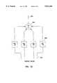
- FIG. 2illustrates a block diagram of the inspection system.
- the control electronics 26 of the metrology unitare driven by a precision motion control unit 38 which receives and interprets commands from a computer 40.
- the particular scanner positioning stage 22provides a range of motion which can be varied according to need. In the preferred embodiment, the stage has a range of motion of 8 inches in the X direction and 4 inches in the Y direction with 0.1 micron resolution.
- a separate scanner interface 42provides high speed image acquisition and timing.
- the video memory board 44is used to store image data from the scanner 16 and to perform bit manipulation of the image. Data from the video memory 44 is sent to the optional image processor 46 and overlaid with the VGA graphics 48 for displaying the images on computer 40.
- the computer 40is used to manipulate the collected data.
- the grid array inspection system 10thereby can provide two dimensional (intensity) data and a three dimensional (height) data. All control electronics including the computers are housed in the base 20.
- FIG. 3illustrates a dual detector configuration which may be utilized to further eliminate occlusion effects and reduce specular reflections and errors caused by secondary reflections.
- a laser 50scans across a grid array package 52.
- Receiver #1 54 and Receiver #2 56collect the scanned image and route the information to the laser scanner electronics 58. Thereafter, the image is routed to the computer 60 for displaying.
- the grid inspection assemblygathers data pertaining to pin grid assemblies 70 as illustrated in FIG. 4.
- the inspection system 10performs high speed, high accuracy data collection pixel-by-pixel for the image illuminated by the three-dimensional scanner 16.
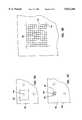
- the operatorfirst identifies the type of pin grid array being inspected and enters the identification code into the computer. As illustrated in FIG. 5A, the computer matches the identification code to a coarse alignment grid 82 from a data file.
- the coarse position grid 82consists of a block of predetermined dimension containing pixel data representing the height measurement for each pixel 86.
- Each pixel 86represents roughly a 0.001 inch by 0.002 inch area.
- Pin 84 height levelsare based on 0.001 inch per level of gray scale. The gray scale ranges from 0 to 255 therefore a pin height of 0 to 0.255 inches is capable of being measured.
- the individual values representing the height data for that pixel 86facilitates the determination of the height and physical location of each pin 84.
- FIG. 5Cillustrates the location of the tip 88 of a pin 84.
- the algorithmperforms a fine search 90 of the image for pixels 86 which represent the tip 88 of the pin 84.
- the height value for the tip 88 of the pin 84will be significantly greater than the surrounding height values representing the bottom surface 92 of the grid array package 80.
- coplanarity and regression plotscan be developed and analyzed. Limits can be set within the algorithm such that the grid array package can be rejected based upon the detection of deviations from the boundary limits with respect to height, position, coplanarity, and regression.
- FIG. 6Aillustrates a side view of a typical compound bend 100.
- Two-dimensional and three-dimensional image processing of the present inventionenables the detection of compound bends 100 in pins 102 on pin grid array packages 104.
- FIG. 6Billustrates a top view of a compound bend 100.
- Compound bendsare generally characterized by height data in the range between what the base of the pin grid array shows and that of the tip. The sensor does not always accurately detect the compound bend from the height data due to the nearly vertical slope of the lead which scatters the laser energy. But due to this phenomenon, the two-dimensional (intensity) image of a compound bend can be characterized by a dark region where the compound bend is.
- the compound bend detection techniquestherefore exploit both the two-dimensional (intensity) imagery as well as the three-dimensional (height) imagery.
- FIG. 7illustrates the first method which uses an algorithm to analyze the height levels between pixel 110 values around the identified tip 112 of the pin in the three-dimensional image. Using histogram techniques, the algorithm identifies the compound bend 114 as existing when there is a relatively large number of high pixels in the area of interest around the pin.
- the second methodis similar to the first but analyzes the intensity image. Using histogram techniques, the algorithm identifies a compound bend when there is a relatively large number of dark pixels in the area of interest.
- FIG. 8illustrates the third method which involves performing a radial profile measurement around the tip 120 of the pin in the three-dimensional image.
- the height pixel value 122 along a line 124 of pixels extending outward away from the tip 120 of the pinis added.
- the sum of the height pixel values (Z profile) along each linewill be approximately the same except where the compound bend exists 126.
- the levelwill deviate from the other radial profile values due to the high pixel values representing the portion of the pin protruding from the axis.
- FIG. 9illustrates a plot of the radial profile.
- the plotsillustrates a smooth curve having an upward protrusion 130 at the location of the compound bend.
- the fourth methodis similar to the third method, but uses intensity data instead.
- the radial profilesare analyzed to find the lowest values. A relatively low value is indicative of a probable compound bend.
- the final methodinvolves performing tangent profile measurements around the tip.
- FIG. 10illustrates this method. Two lines of pixels 150,152 substantially tangent to the tip of the pin 154 and parallel to one another are selected. The height values for each pixel represented by the portion 156 of the tangent extending beyond the tip and to one side of the pin 154 are added. The orientation of the tangents are rotated around the pin 154 and additional measurements are taken. The tangent profiles are computed and result in a dark to light transition plot and a light to dark transition plot.
- FIG. 11illustrates the plot of the light to dark 160 and dark to light 162 transitions. The location of a compound bend is found at the edge of the transitions in the plots.
- the location of the compound bend 130occurs where a transition from dark to light aligns with a transition from light to dark.
- the tangent profile methodresults in a substantially better indication of the location of subtle compound bends than other methods.
- the location parameters from the five methodsare combined using fuzzy logic to weigh each method.
- the most distinctive identification of a compound bendrelies on the tangent profile and Z profile method.
- the first, second and fourth methodsare given a weight of zero or near zero.
- the weight values given to the other methodscould be modified.
- a ball grid assemblyis inspected.
- the operatorfirst identifies the type of ball grid array being inspected and enters the identification code into the computer.
- the computeragain matches the identification code to a coarse alignment grid from a data file.
- each solder ballAfter the coarse location of each ball is identified, the position of each solder ball is located by matching X and Y projections (profiles).
- FIG. 12illustrates the method for finding the location of a ball grid.
- the matchingis performed by taking each profile entry 200, multiplying it by a weighting factor 202, and adding 204 the resulting products. This process is repeated for each potential location and the location corresponding to the greatest sum represents the position of the solder ball. A three sample interpolation is used to get sub-pixel location. This process is the same for both X and Y profiles.
- the algorithm used for finding the position of a ballis similar to an artificial neural net algorithm, but with only one neuron. In neural net terms it would be called a single element, single layer perceptron.
- the weighting factors 202are optimized to give a high output 206 when the position of the ball is located.
- the optimization of the weighting factors 202is performed using the Widrow-Hoff equation.
- the Windrow-Hoff equationis equivalent to the back propagation algorithm when there is only one neuron.
- FIG. 13shows a typical profile for a ball 210 as well as an aligned 212 and unaligned window 214.
- the length of the windowis dependent upon the number of inputs to the perceptron.
- the perceptronprovides a positive output when the window is aligned 212, and a negative output when the window is not aligned 214.
- Nis the number of inputs to the perception
- P(i)is the ith element in the profile
- W iis the ith coefficient for the perceptron.
- the weighting factorsare optimized to cause the window to be aligned with the position of the solder ball.
- jj o
- O jis equal to 1.
- O jis equal to -1.
- the output of the perceptronis positive only when the window is aligned.
- the adaptation processuses these values as desired outputs, and adjusts the coefficient according to the Widrow-Hoff equation.
- the Widrow-Hoff equationis expressed as follows:
- D jis the desired output at offset j
- ⁇is a constant that sets the adaptation speed.
- the n and n+1 double subscript on Windicates the value before and after an iteration.
- the Widrow-Hoff ruleis applied repeatedly to optimize the weighting coefficients.
- the height of each solder ballcan be determine. Thereafter, coplanarity and regression data can be gathered and the ball grid assembly analyzed for deviations from desired specifications.
- the grid array inspection systemcan also measure element spacing, lead height, coplanarity, standoff, grid pitch, ball diameter, ball position, and package warp from the height and position data.
Landscapes
- Physics & Mathematics (AREA)
- Health & Medical Sciences (AREA)
- Life Sciences & Earth Sciences (AREA)
- Chemical & Material Sciences (AREA)
- Analytical Chemistry (AREA)
- Biochemistry (AREA)
- General Health & Medical Sciences (AREA)
- General Physics & Mathematics (AREA)
- Immunology (AREA)
- Pathology (AREA)
- Length Measuring Devices By Optical Means (AREA)
- Investigating Materials By The Use Of Optical Means Adapted For Particular Applications (AREA)
- Testing Or Measuring Of Semiconductors Or The Like (AREA)
Abstract
Description
W.sub.i.sbsb.n+1 =W.sub.i.sbsb.n +μ(D.sub.j -O.sub.j)P(i+j)
Claims (6)
Priority Applications (1)
| Application Number | Priority Date | Filing Date | Title |
|---|---|---|---|
| US08/850,286US5812268A (en) | 1993-10-19 | 1997-05-05 | Grid array inspection system and method |
Applications Claiming Priority (2)
| Application Number | Priority Date | Filing Date | Title |
|---|---|---|---|
| US08/138,776US5652658A (en) | 1993-10-19 | 1993-10-19 | Grid array inspection system and method |
| US08/850,286US5812268A (en) | 1993-10-19 | 1997-05-05 | Grid array inspection system and method |
Related Parent Applications (1)
| Application Number | Title | Priority Date | Filing Date |
|---|---|---|---|
| US08/138,776ContinuationUS5652658A (en) | 1993-10-19 | 1993-10-19 | Grid array inspection system and method |
Publications (1)
| Publication Number | Publication Date |
|---|---|
| US5812268Atrue US5812268A (en) | 1998-09-22 |
Family
ID=22483590
Family Applications (2)
| Application Number | Title | Priority Date | Filing Date |
|---|---|---|---|
| US08/138,776Expired - LifetimeUS5652658A (en) | 1993-10-19 | 1993-10-19 | Grid array inspection system and method |
| US08/850,286Expired - LifetimeUS5812268A (en) | 1993-10-19 | 1997-05-05 | Grid array inspection system and method |
Family Applications Before (1)
| Application Number | Title | Priority Date | Filing Date |
|---|---|---|---|
| US08/138,776Expired - LifetimeUS5652658A (en) | 1993-10-19 | 1993-10-19 | Grid array inspection system and method |
Country Status (5)
| Country | Link |
|---|---|
| US (2) | US5652658A (en) |
| EP (1) | EP0724773B1 (en) |
| JP (1) | JP3005294B2 (en) |
| DE (1) | DE69426082T2 (en) |
| WO (1) | WO1995011519A1 (en) |
Cited By (13)
| Publication number | Priority date | Publication date | Assignee | Title |
|---|---|---|---|---|
| US6055054A (en)* | 1997-05-05 | 2000-04-25 | Beaty; Elwin M. | Three dimensional inspection system |
| US6061645A (en)* | 1996-12-31 | 2000-05-09 | Datalogic S.P.A. | Process and apparatus for measuring the volume of an object |
| US6064757A (en)* | 1998-01-16 | 2000-05-16 | Elwin M. Beaty | Process for three dimensional inspection of electronic components |
| WO2001004567A3 (en)* | 1999-07-13 | 2001-05-03 | Beaty Elwin M | Method and apparatus for three dimensional inspection of electronic components |
| US6260001B1 (en)* | 1996-12-31 | 2001-07-10 | Datalogic S.P.A. | Process and apparatus for measuring the volume of an object by means of a laser scanner |
| US20030011761A1 (en)* | 1999-12-23 | 2003-01-16 | Tally Gilat-Bernshtein | Cam reference for inspection of multi-color and contour images |
| US6518997B1 (en)* | 1998-08-05 | 2003-02-11 | National Semiconductor Corporation | Grid array inspection system and method |
| US6517004B2 (en)* | 1995-12-18 | 2003-02-11 | Metrologic Instruments, Inc. | Automated system for identifying and dimensioning packages transported through a laser scanning tunnel using laser scanning beam indexing techniques |
| US20040085549A1 (en)* | 2000-12-29 | 2004-05-06 | Carl Smets | Method and an apparatus for measuring positions of contact elements of an electronic component |
| US6915007B2 (en) | 1998-01-16 | 2005-07-05 | Elwin M. Beaty | Method and apparatus for three dimensional inspection of electronic components |
| US20050190961A1 (en)* | 1998-01-16 | 2005-09-01 | Beaty Elwin M. | Method of manufacturing electronic components including a method for three dimensional inspection |
| US20100092041A1 (en)* | 2008-10-13 | 2010-04-15 | Koh Young Technology Inc. | Method of measuring a three-dimensional shape |
| CN110680371A (en)* | 2019-10-21 | 2020-01-14 | 华中科技大学 | A method and device for imaging internal and external structures of human body based on structured light and CT |
Families Citing this family (22)
| Publication number | Priority date | Publication date | Assignee | Title |
|---|---|---|---|---|
| JP3158966B2 (en)* | 1995-06-19 | 2001-04-23 | 松下電器産業株式会社 | Manufacturing apparatus and manufacturing method of electronic component with bump |
| US5978502A (en) | 1996-04-01 | 1999-11-02 | Cognex Corporation | Machine vision methods for determining characteristics of three-dimensional objects |
| US6130959A (en)* | 1997-07-16 | 2000-10-10 | Cognex Corporation | Analyzing an image of an arrangement of discrete objects |
| US6118893A (en) | 1997-07-16 | 2000-09-12 | Cognex Corporation | Analysis of an image of a pattern of discrete objects |
| US6151406A (en) | 1997-10-09 | 2000-11-21 | Cognex Corporation | Method and apparatus for locating ball grid array packages from two-dimensional image data |
| US6055328A (en)* | 1998-01-16 | 2000-04-25 | Cognex Corporation | Analyzing an acquired arrangement of object locations |
| US6067376A (en)* | 1998-01-16 | 2000-05-23 | Cognex Corporation | Classifying pixels of an image |
| US6633663B1 (en) | 1998-05-05 | 2003-10-14 | International Business Machines Corporation | Method and system for determining component dimensional information |
| US6301549B1 (en) | 1998-06-26 | 2001-10-09 | Lucent Technologies, Inc. | Three dimensional object boundary and motion determination device and method of operation thereof |
| US7034272B1 (en)* | 1999-10-05 | 2006-04-25 | Electro Scientific Industries, Inc. | Method and apparatus for evaluating integrated circuit packages having three dimensional features |
| US6525331B1 (en) | 1999-12-01 | 2003-02-25 | Nanyang Technological University | Ball grid array (BGA) package on-line non-contact inspection method and system |
| US6665066B2 (en)* | 2001-04-27 | 2003-12-16 | National Instruments Corporation | Machine vision system and method for analyzing illumination lines in an image to determine characteristics of an object being inspected |
| WO2005024403A1 (en)* | 2003-09-05 | 2005-03-17 | Semiconductor Technologies & Instruments Pte Ltd. | Ball grid array inspection system and method |
| US7315383B1 (en)* | 2004-07-09 | 2008-01-01 | Mohsen Abdollahi | Scanning 3D measurement technique using structured lighting and high-speed CMOS imager |
| US7639861B2 (en) | 2005-09-14 | 2009-12-29 | Cognex Technology And Investment Corporation | Method and apparatus for backlighting a wafer during alignment |
| US8111904B2 (en) | 2005-10-07 | 2012-02-07 | Cognex Technology And Investment Corp. | Methods and apparatus for practical 3D vision system |
| US8162584B2 (en) | 2006-08-23 | 2012-04-24 | Cognex Corporation | Method and apparatus for semiconductor wafer alignment |
| US8611636B1 (en) | 2009-01-05 | 2013-12-17 | Cognex Corporation | High speed method of aligning components having a plurality of non-uniformly spaced features |
| SG186207A1 (en) | 2010-06-08 | 2013-01-30 | Dcg Systems Inc | Three-dimensional hot spot localization |
| EP2444795A1 (en)* | 2010-10-22 | 2012-04-25 | DCG Systems, Inc. | Lock in thermal laser stimulation through one side of the device while acquiring lock-in thermal emission images on the opposite side |
| US9488469B1 (en) | 2013-04-22 | 2016-11-08 | Cognex Corporation | System and method for high-accuracy measurement of object surface displacement using a laser displacement sensor |
| CN114252455B (en)* | 2021-12-22 | 2025-04-22 | 中核建中核燃料元件有限公司 | Grid appearance automatic detection equipment |
Citations (12)
| Publication number | Priority date | Publication date | Assignee | Title |
|---|---|---|---|---|
| US4240750A (en)* | 1978-10-02 | 1980-12-23 | Hurd William A | Automatic circuit board tester |
| US4373804A (en)* | 1979-04-30 | 1983-02-15 | Diffracto Ltd. | Method and apparatus for electro-optically determining the dimension, location and attitude of objects |
| US4706168A (en)* | 1985-11-15 | 1987-11-10 | View Engineering, Inc. | Systems and methods for illuminating objects for vision systems |
| US4743771A (en)* | 1985-06-17 | 1988-05-10 | View Engineering, Inc. | Z-axis height measurement system |
| US4872052A (en)* | 1986-12-03 | 1989-10-03 | View Engineering, Inc. | Semiconductor device inspection system |
| US4891529A (en)* | 1988-08-22 | 1990-01-02 | View Engineering, Inc. | System and method for analyzing dimensions of can tops during manufacture |
| US5024529A (en)* | 1988-01-29 | 1991-06-18 | Synthetic Vision Systems, Inc. | Method and system for high-speed, high-resolution, 3-D imaging of an object at a vision station |
| US5028799A (en)* | 1988-08-01 | 1991-07-02 | Robotic Vision System, Inc. | Method and apparatus for three dimensional object surface determination using co-planar data from multiple sensors |
| US5058178A (en)* | 1989-12-21 | 1991-10-15 | At&T Bell Laboratories | Method and apparatus for inspection of specular, three-dimensional features |
| US5162866A (en)* | 1989-12-25 | 1992-11-10 | Sony Corporation | Apparatus and method for inspecting IC leads |
| US5192983A (en)* | 1989-12-19 | 1993-03-09 | Matsushita Electric Industrial Co., Ltd. | Apparatus for and method of checking external appearance of soldering state |
| US5206705A (en)* | 1989-12-13 | 1993-04-27 | Matsushita Electric Industrial Co., Ltd. | Method of checking external shape of solder portion |
- 1993
- 1993-10-19USUS08/138,776patent/US5652658A/ennot_activeExpired - Lifetime
- 1994
- 1994-07-22DEDE69426082Tpatent/DE69426082T2/ennot_activeExpired - Fee Related
- 1994-07-22JPJP7511758Apatent/JP3005294B2/ennot_activeExpired - Lifetime
- 1994-07-22EPEP94924008Apatent/EP0724773B1/ennot_activeExpired - Lifetime
- 1994-07-22WOPCT/US1994/008385patent/WO1995011519A1/enactiveIP Right Grant
- 1997
- 1997-05-05USUS08/850,286patent/US5812268A/ennot_activeExpired - Lifetime
Patent Citations (12)
| Publication number | Priority date | Publication date | Assignee | Title |
|---|---|---|---|---|
| US4240750A (en)* | 1978-10-02 | 1980-12-23 | Hurd William A | Automatic circuit board tester |
| US4373804A (en)* | 1979-04-30 | 1983-02-15 | Diffracto Ltd. | Method and apparatus for electro-optically determining the dimension, location and attitude of objects |
| US4743771A (en)* | 1985-06-17 | 1988-05-10 | View Engineering, Inc. | Z-axis height measurement system |
| US4706168A (en)* | 1985-11-15 | 1987-11-10 | View Engineering, Inc. | Systems and methods for illuminating objects for vision systems |
| US4872052A (en)* | 1986-12-03 | 1989-10-03 | View Engineering, Inc. | Semiconductor device inspection system |
| US5024529A (en)* | 1988-01-29 | 1991-06-18 | Synthetic Vision Systems, Inc. | Method and system for high-speed, high-resolution, 3-D imaging of an object at a vision station |
| US5028799A (en)* | 1988-08-01 | 1991-07-02 | Robotic Vision System, Inc. | Method and apparatus for three dimensional object surface determination using co-planar data from multiple sensors |
| US4891529A (en)* | 1988-08-22 | 1990-01-02 | View Engineering, Inc. | System and method for analyzing dimensions of can tops during manufacture |
| US5206705A (en)* | 1989-12-13 | 1993-04-27 | Matsushita Electric Industrial Co., Ltd. | Method of checking external shape of solder portion |
| US5192983A (en)* | 1989-12-19 | 1993-03-09 | Matsushita Electric Industrial Co., Ltd. | Apparatus for and method of checking external appearance of soldering state |
| US5058178A (en)* | 1989-12-21 | 1991-10-15 | At&T Bell Laboratories | Method and apparatus for inspection of specular, three-dimensional features |
| US5162866A (en)* | 1989-12-25 | 1992-11-10 | Sony Corporation | Apparatus and method for inspecting IC leads |
Non-Patent Citations (6)
| Title |
|---|
| "High-speed image processing of 1 Mbyte pictures", SPIE vol. 728, Optics, Illuminations, and Image Sensing for Machine Vision (1986), pp. 111-115. |
| "System Technology/Testing and Manufacturing", 8167 Computer Design, 25 (1986) Mar., No. 6, Littleton, Massachusetts, USA. |
| §21.4 from brochure relating to Spatial Resolution and Frame Rate Reduction Techniques. |
| 21.4 from brochure relating to Spatial Resolution and Frame Rate Reduction Techniques.* |
| High speed image processing of 1 Mbyte pictures , SPIE vol. 728, Optics, Illuminations, and Image Sensing for Machine Vision (1986), pp. 111 115.* |
| System Technology/Testing and Manufacturing , 8167 Computer Design, 25 (1986) Mar., No. 6, Littleton, Massachusetts, USA.* |
Cited By (25)
| Publication number | Priority date | Publication date | Assignee | Title |
|---|---|---|---|---|
| US6517004B2 (en)* | 1995-12-18 | 2003-02-11 | Metrologic Instruments, Inc. | Automated system for identifying and dimensioning packages transported through a laser scanning tunnel using laser scanning beam indexing techniques |
| US6260001B1 (en)* | 1996-12-31 | 2001-07-10 | Datalogic S.P.A. | Process and apparatus for measuring the volume of an object by means of a laser scanner |
| US6061645A (en)* | 1996-12-31 | 2000-05-09 | Datalogic S.P.A. | Process and apparatus for measuring the volume of an object |
| US6055054A (en)* | 1997-05-05 | 2000-04-25 | Beaty; Elwin M. | Three dimensional inspection system |
| US6915007B2 (en) | 1998-01-16 | 2005-07-05 | Elwin M. Beaty | Method and apparatus for three dimensional inspection of electronic components |
| US20050190960A1 (en)* | 1998-01-16 | 2005-09-01 | Beaty Elwin M. | Electronic component products made according to a process that includes a method for three dimensional inspection |
| US6072898A (en)* | 1998-01-16 | 2000-06-06 | Beaty; Elwin M. | Method and apparatus for three dimensional inspection of electronic components |
| US7085411B2 (en) | 1998-01-16 | 2006-08-01 | Scanner Technologies Corporation | Method of manufacturing electronic components including a method for three dimensional inspection |
| US7079678B2 (en) | 1998-01-16 | 2006-07-18 | Scanner Technologies Corporation | Electronic component products made according to a process that includes a method for three dimensional inspection |
| US6064756A (en)* | 1998-01-16 | 2000-05-16 | Elwin M. Beaty | Apparatus for three dimensional inspection of electronic components |
| US20050189657A1 (en)* | 1998-01-16 | 2005-09-01 | Beaty Elwin M. | Electronic component products and method of manufacturing electronic component products |
| US6862365B1 (en) | 1998-01-16 | 2005-03-01 | Elwin Beaty & Elaine Beaty | Method and apparatus for three dimensional inspection of electronic components |
| US6064757A (en)* | 1998-01-16 | 2000-05-16 | Elwin M. Beaty | Process for three dimensional inspection of electronic components |
| US20050190961A1 (en)* | 1998-01-16 | 2005-09-01 | Beaty Elwin M. | Method of manufacturing electronic components including a method for three dimensional inspection |
| US7508974B2 (en) | 1998-01-16 | 2009-03-24 | Scanner Technologies Corporation | Electronic component products and method of manufacturing electronic component products |
| US6518997B1 (en)* | 1998-08-05 | 2003-02-11 | National Semiconductor Corporation | Grid array inspection system and method |
| WO2001004567A3 (en)* | 1999-07-13 | 2001-05-03 | Beaty Elwin M | Method and apparatus for three dimensional inspection of electronic components |
| US20030011761A1 (en)* | 1999-12-23 | 2003-01-16 | Tally Gilat-Bernshtein | Cam reference for inspection of multi-color and contour images |
| US7218771B2 (en)* | 1999-12-23 | 2007-05-15 | Orbotech, Ltd. | Cam reference for inspection of contour images |
| US20070223804A1 (en)* | 1999-12-23 | 2007-09-27 | Orbotech Ltd | CAM reference for inspection of contour images |
| US20040085549A1 (en)* | 2000-12-29 | 2004-05-06 | Carl Smets | Method and an apparatus for measuring positions of contact elements of an electronic component |
| US7423743B2 (en) | 2000-12-29 | 2008-09-09 | Icos Vision Systems Nv | Method and an apparatus for measuring positions of contact elements of an electronic component |
| US20100092041A1 (en)* | 2008-10-13 | 2010-04-15 | Koh Young Technology Inc. | Method of measuring a three-dimensional shape |
| US8437533B2 (en)* | 2008-10-13 | 2013-05-07 | Koh Young Technology Inc. | Method of measuring a three-dimensional shape |
| CN110680371A (en)* | 2019-10-21 | 2020-01-14 | 华中科技大学 | A method and device for imaging internal and external structures of human body based on structured light and CT |
Also Published As
| Publication number | Publication date |
|---|---|
| WO1995011519A1 (en) | 1995-04-27 |
| JPH09505886A (en) | 1997-06-10 |
| JP3005294B2 (en) | 2000-01-31 |
| DE69426082D1 (en) | 2000-11-09 |
| EP0724773B1 (en) | 2000-10-04 |
| US5652658A (en) | 1997-07-29 |
| EP0724773A1 (en) | 1996-08-07 |
| DE69426082T2 (en) | 2001-06-07 |
Similar Documents
| Publication | Publication Date | Title |
|---|---|---|
| US5812268A (en) | Grid array inspection system and method | |
| US6173070B1 (en) | Machine vision method using search models to find features in three dimensional images | |
| US5859924A (en) | Method and system for measuring object features | |
| KR100334862B1 (en) | Method and system for three-dimensional imaging based on triangulation | |
| US5812269A (en) | Triangulation-based 3-D imaging and processing method and system | |
| EP0638801B1 (en) | Method of inspecting the array of balls of an integrated circuit module | |
| EP0713593B1 (en) | Method and apparatus for ball bond inspection system | |
| EP0160781B1 (en) | Measuring and detecting printed circuit wiring defects | |
| US5546189A (en) | Triangulation-based 3D imaging and processing method and system | |
| US6064757A (en) | Process for three dimensional inspection of electronic components | |
| US6606788B1 (en) | Component recognizing method and apparatus | |
| JP4901903B2 (en) | 3D inspection system | |
| US20040179207A1 (en) | Method and system for high speed measuring of microscopic targets | |
| US6118538A (en) | Method and apparatus for electronic component lead measurement using light based sensors on a component placement machine | |
| US11953312B2 (en) | System and method of object inspection using multispectral 3D laser scanning | |
| US6525331B1 (en) | Ball grid array (BGA) package on-line non-contact inspection method and system | |
| EP0848245B1 (en) | Method and apparatus for measuring the height of an object | |
| JPH02278103A (en) | Three-dimensional inspection method and device for printed circuit boards | |
| JP2877061B2 (en) | Coplanarity inspection equipment | |
| US20040263862A1 (en) | Detecting peripheral points of reflected radiation beam spots for topographically mapping a surface | |
| Qixin et al. | A binocular machine vision system for ball grid array package inspection | |
| JP3481704B2 (en) | Height measuring method and device | |
| JPH0666401B2 (en) | Inspection method for lead frame | |
| JP2525261B2 (en) | Mounted board visual inspection device | |
| JP2929828B2 (en) | IC lead inspection method and device |
Legal Events
| Date | Code | Title | Description |
|---|---|---|---|
| STCF | Information on status: patent grant | Free format text:PATENTED CASE | |
| FPAY | Fee payment | Year of fee payment:4 | |
| AS | Assignment | Owner name:GSI LUMONICS CORPORATION, MICHIGAN Free format text:ASSIGNMENT OF ASSIGNORS INTEREST;ASSIGNOR:GENERAL SCANNING, INC.;REEL/FRAME:013751/0518 Effective date:20030623 | |
| FPAY | Fee payment | Year of fee payment:8 | |
| FPAY | Fee payment | Year of fee payment:12 | |
| AS | Assignment | Owner name:THE BANK OF NEW YORK MELLON TRUST COMPANY, N.A., A Free format text:SECURITY AGREEMENT;ASSIGNORS:GSI GROUP INC.;GSI GROUP CORPORATION;MES INTERNATIONAL INC.;AND OTHERS;REEL/FRAME:024755/0537 Effective date:20100723 | |
| AS | Assignment | Owner name:GSI GROUP CORPORATION, MASSACHUSETTS Free format text:CHANGE OF NAME;ASSIGNOR:GSI LUMONICS CORPORATION;REEL/FRAME:027074/0517 Effective date:20050627 | |
| AS | Assignment | Owner name:BANK OF AMERICA, N.A., MASSACHUSETTS Free format text:SECURITY AGREEMENT;ASSIGNORS:GSI GROUP INC.;GSI GROUP CORPORATION;REEL/FRAME:027128/0763 Effective date:20111019 Owner name:MICROE SYSTEMS CORP., MASSACHUSETTS Free format text:RELEASE;ASSIGNOR:THE BANK OF NEW YORK MELLON TRUST COMPANY, N.A.;REEL/FRAME:027127/0368 Effective date:20111019 Owner name:EXCEL TECHNOLOGY INC., MASSACHUSETTS Free format text:RELEASE;ASSIGNOR:THE BANK OF NEW YORK MELLON TRUST COMPANY, N.A.;REEL/FRAME:027127/0368 Effective date:20111019 Owner name:SYNRAD INC., MASSACHUSETTS Free format text:RELEASE;ASSIGNOR:THE BANK OF NEW YORK MELLON TRUST COMPANY, N.A.;REEL/FRAME:027127/0368 Effective date:20111019 Owner name:THE OPTICAL CORPORATION, MASSACHUSETTS Free format text:RELEASE;ASSIGNOR:THE BANK OF NEW YORK MELLON TRUST COMPANY, N.A.;REEL/FRAME:027127/0368 Effective date:20111019 Owner name:GSI GROUP CORPORATION, MASSACHUSETTS Free format text:RELEASE;ASSIGNOR:THE BANK OF NEW YORK MELLON TRUST COMPANY, N.A.;REEL/FRAME:027127/0368 Effective date:20111019 Owner name:CAMBRIDGE TECHNOLOGY INC., MASSACHUSETTS Free format text:RELEASE;ASSIGNOR:THE BANK OF NEW YORK MELLON TRUST COMPANY, N.A.;REEL/FRAME:027127/0368 Effective date:20111019 Owner name:CONTROL LASER CORPORATION (D/B/A BAUBLYS CONTROL L Free format text:RELEASE;ASSIGNOR:THE BANK OF NEW YORK MELLON TRUST COMPANY, N.A.;REEL/FRAME:027127/0368 Effective date:20111019 Owner name:QUANTRONIX CORPORATION, MASSACHUSETTS Free format text:RELEASE;ASSIGNOR:THE BANK OF NEW YORK MELLON TRUST COMPANY, N.A.;REEL/FRAME:027127/0368 Effective date:20111019 Owner name:CONTINUUM ELECTRO-OPTICS INC., MASSACHUSETTS Free format text:RELEASE;ASSIGNOR:THE BANK OF NEW YORK MELLON TRUST COMPANY, N.A.;REEL/FRAME:027127/0368 Effective date:20111019 Owner name:PHOTO RESEARCH INC., MASSACHUSETTS Free format text:RELEASE;ASSIGNOR:THE BANK OF NEW YORK MELLON TRUST COMPANY, N.A.;REEL/FRAME:027127/0368 Effective date:20111019 Owner name:GSI GROUP INC., MASSACHUSETTS Free format text:RELEASE;ASSIGNOR:THE BANK OF NEW YORK MELLON TRUST COMPANY, N.A.;REEL/FRAME:027127/0368 Effective date:20111019 Owner name:MES INTERNATIONAL INC., MASSACHUSETTS Free format text:RELEASE;ASSIGNOR:THE BANK OF NEW YORK MELLON TRUST COMPANY, N.A.;REEL/FRAME:027127/0368 Effective date:20111019 | |
| AS | Assignment | Owner name:GSI GROUP CORPORATION, MASSACHUSETTS Free format text:RELEASE OF SECURITY INTEREST IN PATENTS RECORDED AT R/F 027128/0763;ASSIGNOR:BANK OF AMERICA, N.A., AS ADMINISTRATIVE AGENT;REEL/FRAME:030341/0956 Effective date:20130503 | |
| AS | Assignment | Owner name:ELECTRO SCIENTIFIC INDUSTRIES, INC., OREGON Free format text:ASSIGNMENT OF ASSIGNORS INTEREST;ASSIGNORS:GSI GROUP CORPORATION;GSI GROUP INC;REEL/FRAME:030582/0160 Effective date:20130503 | |
| AS | Assignment | Owner name:ELECTRO SCIENTIFIC INDUSTRIES, INC., OREGON Free format text:CORRECTIVE ASSIGNMENT TO CORRECT THE APPLICATION SERIAL NUMBER 11776904 PREVIOUSLY RECORDED ON REEL 030582 FRAME 0160. ASSIGNOR(S) HEREBY CONFIRMS THE ASSIGNMENT;ASSIGNORS:GSI GROUP CORPORATION;GSI GROUP INC.;REEL/FRAME:056424/0287 Effective date:20130503 |