US5811325A - Method of making a polysilicon carbon source/drain heterojunction thin-film transistor - Google Patents
Method of making a polysilicon carbon source/drain heterojunction thin-film transistorDownload PDFInfo
- Publication number
- US5811325A US5811325AUS08/775,603US77560396AUS5811325AUS 5811325 AUS5811325 AUS 5811325AUS 77560396 AUS77560396 AUS 77560396AUS 5811325 AUS5811325 AUS 5811325A
- Authority
- US
- United States
- Prior art keywords
- layer
- amorphous silicon
- oxide layer
- polysilicon
- forming
- Prior art date
- Legal status (The legal status is an assumption and is not a legal conclusion. Google has not performed a legal analysis and makes no representation as to the accuracy of the status listed.)
- Expired - Lifetime
Links
- 229910021420polycrystalline siliconInorganic materials0.000titleclaimsabstractdescription76
- 229920005591polysiliconPolymers0.000titleclaimsabstractdescription76
- OKTJSMMVPCPJKN-UHFFFAOYSA-NCarbonChemical compound[C]OKTJSMMVPCPJKN-UHFFFAOYSA-N0.000titleclaimsabstractdescription41
- 229910052799carbonInorganic materials0.000titleclaimsabstractdescription41
- 239000010409thin filmSubstances0.000titleclaimsdescription13
- 238000004519manufacturing processMethods0.000titledescription4
- 229910021417amorphous siliconInorganic materials0.000claimsabstractdescription89
- 229920002120photoresistant polymerPolymers0.000claimsabstractdescription57
- HMDDXIMCDZRSNE-UHFFFAOYSA-N[C].[Si]Chemical compound[C].[Si]HMDDXIMCDZRSNE-UHFFFAOYSA-N0.000claimsabstractdescription39
- 238000000137annealingMethods0.000claimsabstractdescription27
- 239000000758substrateSubstances0.000claimsabstractdescription18
- 230000001131transforming effectEffects0.000claimsabstractdescription10
- 238000000034methodMethods0.000claimsdescription106
- VYPSYNLAJGMNEJ-UHFFFAOYSA-NSilicium dioxideChemical compoundO=[Si]=OVYPSYNLAJGMNEJ-UHFFFAOYSA-N0.000claimsdescription23
- 238000004518low pressure chemical vapour depositionMethods0.000claimsdescription16
- 238000002161passivationMethods0.000claimsdescription14
- BOTDANWDWHJENH-UHFFFAOYSA-NTetraethyl orthosilicateChemical groupCCO[Si](OCC)(OCC)OCCBOTDANWDWHJENH-UHFFFAOYSA-N0.000claimsdescription11
- 229910052751metalInorganic materials0.000claimsdescription10
- 239000002184metalSubstances0.000claimsdescription10
- 238000000623plasma-assisted chemical vapour depositionMethods0.000claimsdescription10
- 238000005224laser annealingMethods0.000claimsdescription8
- 238000000206photolithographyMethods0.000claimsdescription8
- 229910052782aluminiumInorganic materials0.000claimsdescription7
- XAGFODPZIPBFFR-UHFFFAOYSA-NaluminiumChemical compound[Al]XAGFODPZIPBFFR-UHFFFAOYSA-N0.000claimsdescription6
- 239000011521glassSubstances0.000claimsdescription4
- 238000010586diagramMethods0.000description11
- 239000008186active pharmaceutical agentSubstances0.000description9
- 230000000694effectsEffects0.000description3
- 239000004973liquid crystal related substanceSubstances0.000description3
- 230000005641tunnelingEffects0.000description3
- 229910004012SiCxInorganic materials0.000description2
- 229910004205SiNXInorganic materials0.000description2
- 239000000203mixtureSubstances0.000description2
- 239000004065semiconductorSubstances0.000description2
- 238000004544sputter depositionMethods0.000description2
- 229910003944H3 PO4Inorganic materials0.000description1
- GRYLNZFGIOXLOG-UHFFFAOYSA-NNitric acidChemical compoundO[N+]([O-])=OGRYLNZFGIOXLOG-UHFFFAOYSA-N0.000description1
- 239000000370acceptorSubstances0.000description1
- 230000004888barrier functionEffects0.000description1
- 230000007423decreaseEffects0.000description1
- 238000000151depositionMethods0.000description1
- 230000008021depositionEffects0.000description1
- 239000002019doping agentSubstances0.000description1
- 230000005684electric fieldEffects0.000description1
- 239000000463materialSubstances0.000description1
- 238000012986modificationMethods0.000description1
- 230000004048modificationEffects0.000description1
- 229910017604nitric acidInorganic materials0.000description1
- 238000001020plasma etchingMethods0.000description1
Images


Classifications
- H—ELECTRICITY
- H10—SEMICONDUCTOR DEVICES; ELECTRIC SOLID-STATE DEVICES NOT OTHERWISE PROVIDED FOR
- H10D—INORGANIC ELECTRIC SEMICONDUCTOR DEVICES
- H10D30/00—Field-effect transistors [FET]
- H10D30/01—Manufacture or treatment
- H10D30/021—Manufacture or treatment of FETs having insulated gates [IGFET]
- H10D30/031—Manufacture or treatment of FETs having insulated gates [IGFET] of thin-film transistors [TFT]
- H10D30/0312—Manufacture or treatment of FETs having insulated gates [IGFET] of thin-film transistors [TFT] characterised by the gate electrodes
- H10D30/0316—Manufacture or treatment of FETs having insulated gates [IGFET] of thin-film transistors [TFT] characterised by the gate electrodes of lateral bottom-gate TFTs comprising only a single gate
- H—ELECTRICITY
- H10—SEMICONDUCTOR DEVICES; ELECTRIC SOLID-STATE DEVICES NOT OTHERWISE PROVIDED FOR
- H10D—INORGANIC ELECTRIC SEMICONDUCTOR DEVICES
- H10D30/00—Field-effect transistors [FET]
- H10D30/01—Manufacture or treatment
- H10D30/021—Manufacture or treatment of FETs having insulated gates [IGFET]
- H10D30/031—Manufacture or treatment of FETs having insulated gates [IGFET] of thin-film transistors [TFT]
- H10D30/0321—Manufacture or treatment of FETs having insulated gates [IGFET] of thin-film transistors [TFT] comprising silicon, e.g. amorphous silicon or polysilicon
- H—ELECTRICITY
- H10—SEMICONDUCTOR DEVICES; ELECTRIC SOLID-STATE DEVICES NOT OTHERWISE PROVIDED FOR
- H10D—INORGANIC ELECTRIC SEMICONDUCTOR DEVICES
- H10D30/00—Field-effect transistors [FET]
- H10D30/60—Insulated-gate field-effect transistors [IGFET]
- H10D30/67—Thin-film transistors [TFT]
- H10D30/6704—Thin-film transistors [TFT] having supplementary regions or layers in the thin films or in the insulated bulk substrates for controlling properties of the device
- H10D30/6713—Thin-film transistors [TFT] having supplementary regions or layers in the thin films or in the insulated bulk substrates for controlling properties of the device characterised by the properties of the source or drain regions, e.g. compositions or sectional shapes
Definitions
- the present inventionrelates to a thin-film transistor, and particularly to a polysilicon carbon source/drain heterojunction thin-film transistor.
- Amorphous siliconis used in the deposition of thin-film transistor (TFT) for liquid-crystal displays.
- TFTthin-film transistor
- Amorphous semiconductorsdo not have a crystalline lattice, and this specific disordered nature results in a large number of localized states with energy within the energy gap.
- the localized states in the upper and lower half of the gapbehave like acceptors and donors respectively, which are used to implement a switching element for the liquid-crystal display (LCD).
- LCDliquid-crystal display
- High-mobility polysiliconis therefore a candidate for manufacturing TFTs on the liquid-crystal display.
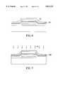
- FIG. 1Ashows the cross-sectional view of a conventional TFT with a gate, a n+ polysilicon drain region and a n+ polysilicon drain region designated respectively as 10, 12 and 14. At least 5 volts is usually applied between the drain 14 and the source region 12 during its operation.
- V GSgate-to-source voltage
- V ththreshold voltage
- 1Bshows an energy band diagram when no V DS voltage bias is applied and the gate voltage V GS is less than V th , where the TFT behaves as a natural p-n junction, and where subscript c designates the conduction band, v the valence band, F the firmi level, and n, p the polarity of the material for the TFT.
- V GSAs the gate voltage V GS is less than V th and the drain 14 -to- source 12 is biased in a normal operation, most part of V DS is dropped at the p-n depletion junction near the drain 14.
- the aforementioned generated holes on the left p sideare apt to go over the barrier according to the quantum tunneling effect due to its narrow width 16 as shown in FIG. 1C, even an offset regions 18 (FIG. 1A) are provided.
- a methodfor forming a polysilicon carbon source/drain heterojunction thin-film transistor that substantially decreases leakage current under reverse voltage bias.
- the presentincludes forming a conductive layer on a substrate, followed by forming a first photoresist layer on the conductive layer, wherein the first photoresist layer defines a gate area over a portion of the substrate. Portions of the conductive layer are then removed using the first photoresist layer as a mask. Next, a first oxide layer is formed over the conductive layer and the substrate, and an amorphous silicon layer is formed on the first oxide layer.
- a second oxide layeris formed on the polysilicon layer.
- a second photoresist layeris formed on the second oxide layer, where the second photoresist layer defines an area aligned to the gate area.
- a heavily-doped amorphous silicon carbon layeris formed over the second oxide layer and the polysilicon layer.
- a third photoresist layeris formed on the heavily-doped polysilicon carbon layer, where the third photoresist layer defines a source/drain area. Portions of the heavily-doped polysilicon carbon layer and the polysilicon layer are then removed using the third photoresist layer as a mask.
- all the steps for forming the polysilicon carbon source/drain heterojunction thin-film transistorare the same as the first embodiment except that an amorphous silicon carbon layer is further formed over the second oxide layer and the polysilicon layer prior forming the heavily-doped amorphous silicon carbon layer. This amorphous silicon carbon layer is subsequently annealed and transformed to a polysilicon carbon layer.
- FIG. 1Ashows the cross-sectional view of a conventional thin-film transistor (TFT).
- TFTthin-film transistor
- FIG. 1Bshows a conventional energy band diagram when V GS is less than threshold voltage V th and no V DS voltage bias is applied to the TFT.
- FIG. 1Cshows a conventional energy band diagram when a normal V DS bias such as 5 volts, and V GS less than V th are applied to the TFT.
- FIGS. 2 to 10show cross-sectional views illustrative of various stages in the fabrication of a polysilicon carbon source/drain heterojunction thin-film transistor in accordance with the first embodiment of the present invention.
- FIG. 11Ashows an energy band diagram when no voltage bias is applied to the TFT in accordance with the first embodiment of the present invention.
- FIG. 11Bshows an energy band diagram when a normal V DS bias such as 5 volts, and V GS less than V th are applied to the TFT in accordance with the first embodiment of the present invention.
- FIGS. 12 to 20show cross-sectional views illustrative of various stages in the fabrication of a polysilicon carbon source/drain heterojunction thin-film transistor in accordance with the second embodiment of the present invention.
- FIG. 21 Ashows an energy band diagram when no voltage bias is applied to the TFT in accordance with the second embodiment of the present invention.
- FIG. 21Bshows an energy band diagram when a normal V DS bias such as 5 volts, and V GS less than V th are applied to the TFT in accordance with the second embodiment of the present invention.
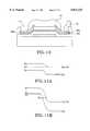
- a conductive layer 20such as a Al or Cr metal layer is formed on a glass substrate 22 using a standard sputtering process, typically to a thickness of about 1500 to 2500 angstroms.
- An alternative way to replace the conductive layer 20is a doped polysilicon layer deposited using a low pressure chemical vapor deposition (LPCVD) process.
- LPCVDlow pressure chemical vapor deposition
- conventional photolithography techniquesare used to define a gate area in a photoresist layer 24 formed on the conductive layer 20.
- the photoresist layer 24is patterned to expose portions of the conductive layer 20 over the substrate 22.
- the conductive layer 20is etched, resulting in a gate region 20 shown in FIG. 3.
- a solution of the mixture of H 3 PO 4 , HNO 3 , CH 3 COOH and H 2 Ois used to etch the aluminum, or a plasma etch process with etchant of SF 6 /Cl 2 is used to etch the doped polysilicon.
- an oxide layer 26, such as amorphous silicon oxide (a-SiOx)is formed over the gate region 20 and the substrate 22 to a thickness of about 1500 to 2500 angstroms, followed by forming an amorphous silicon layer 28 to a thickness of about 500 angstroms.
- a conventional plasma enhanced chemical vapor deposition (PECVD) processis used to form the oxide layer 26 and the amorphous silicon layer 28 for a poly-gate structure. It is noted that the amorphous silicon oxide layer 26 for the poly-gate structure can be replaced by a tetraethoxysilane (TEOS) layer.
- PECVDplasma enhanced chemical vapor deposition
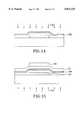
- FIG. 3is then subject to an annealing process 30 such as a standard laser annealing process, so that the amorphous silicon layer 28 is transformed to a polysilicon layer 28A as shown in FIG. 4. It is appreciated that a conventional thermal annealing process could be used instead for the poly-gate structure.
- an annealing process 30such as a standard laser annealing process, so that the amorphous silicon layer 28 is transformed to a polysilicon layer 28A as shown in FIG. 4. It is appreciated that a conventional thermal annealing process could be used instead for the poly-gate structure.
- another oxide layer 32such as amorphous silicon oxide (a-SiO x ), is formed on the polysilicon layer 28A to a thickness of about 2000 ⁇ 3000 angstroms.
- the method used to form this oxide layer 32is the same as the oxide layer 26, and a TEOS layer could be used to replace the oxide layer 32 for the poly-gate structure.
- conventional photolithography techniquesare used to define an area aligned to the gate region 20 in a photoresist layer 34 formed on the oxide layer 32.
- the photoresist layer 34is patterned by a back-side exposure 36 to expose portions of the oxide layer 32.
- n + amorphous silicon carbon (a-SiC x ) layer 38having a thickness of about 300 ⁇ 1000 angstroms.
- a conventional PECVD processis used to form the n + amorphous silicon carbon layer 38 for the metal gate structure, or a standard LPCVD process for the poly-gate structure.
- the n + amorphous silicon carbon layer 38is doped with P + or As + dopants at a concentration of about 10 15 /cm 2 to form a heavily-doped amorphous silicon carbon layer 38.
- FIG. 6The structure of FIG. 6 is then subject to an annealing process 40 such as a laser annealing process, so that the n + amorphous silicon carbon layer 38 is transformed to a n + polysilicon carbon layer 38A as shown in FIG. 7. It is appreciated that a conventional thermal annealing process could be used instead for the poly-gate structure.
- an annealing process 40such as a laser annealing process, so that the n + amorphous silicon carbon layer 38 is transformed to a n + polysilicon carbon layer 38A as shown in FIG. 7. It is appreciated that a conventional thermal annealing process could be used instead for the poly-gate structure.
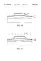
- conventional photolithography techniquesare used to define source/drain area in a photoresist layer 42 formed on the n + polysilicon carbon layer 38A.
- the photoresist layer 42is patterned to expose portions of the n + polysilicon carbon layer 38A.
- the photoresist layer 42as a mask, the n + polysilicon carbon layer 38A and the polysilicon layer 28A are etched, resulting in the structure of FIG. 9.
- a passivation layer 44such as a-SiN x :H is formed over the oxide layer 32, the polysilicon layer 28A and the amorphous silicon oxide layer 26.
- the nominal thickness of the passivation layer 44is about 3000 angstroms, but can also be in the range from about 2000 to 6000 angstroms.
- conventional photolithography techniquesare used to define source/drain contact area in a photoresist layer 46 formed on the passivation layer 44.
- the photoresist layer 46is patterned to expose portions of the passivation layer 44. Using the photoresist layer 44 as a mask, the passivation layer 44 is etched, resulting in source/drain contact regions as shown in FIG. 10.
- the a-SiN x :H layer 44is etched by reactive ion etching using the gas of mixture of CF 4 and O 2 . Subsequently, metal contacts 48 such as aluminum are formed using a conventional sputtering process.
- FIG. 11Ashows an energy band diagram for the resulting polysilicon carbon source/drain heterojunction thin-film transistor (FIG. 10) as no voltage bias is applied.
- V GSgate voltage
- V ththreshold voltage
- the width 50 for the embodiment of the present inventionis larger than the width 16 in FIG. 1C due to the formed heterojunction consisting of the n + polysilicon carbon layer 38A and the polysilicon layer 28A, therefore reducing the tunneling effect and the associated leakage current.
- FIGS. 12 to 20illustrate another embodiment according to the present invention.
- a conductive layer 120such as an aluminum or Cr metal layer is formed on a glass substrate 122.
- An alternative way to replace the conductive layer 120is a doped polysilicon layer deposited using a low pressure chemical vapor deposition (LPCVD) process.
- LPCVDlow pressure chemical vapor deposition
- the conductive layer 120is etched, resulting in a gate region 120 shown in FIG. 13.
- an oxide layer 126such as amorphous silicon oxide (a-SiOx), is formed over the gate region 120 and the substrate 122, followed by forming an amorphous silicon layer 128.
- a-SiOxamorphous silicon oxide
- FIG. 13is then subject to an annealing process 130 such as a standard laser annealing process, so that the amorphous silicon layer 128 is transformed to a polysilicon layer 128A as shown in FIG. 14. It is appreciated that a conventional thermal annealing process could be used instead for the poly-gate structure.
- an annealing process 130such as a standard laser annealing process, so that the amorphous silicon layer 128 is transformed to a polysilicon layer 128A as shown in FIG. 14. It is appreciated that a conventional thermal annealing process could be used instead for the poly-gate structure.
- another oxide layer 132such as amorphous silicon oxide (a-SiO x ), is formed on the polysilicon layer 128A.
- a-SiO xamorphous silicon oxide
- conventional photolithography techniquesare used to define an area aligned to the gate region 120 in a photoresist layer 134 formed on the oxide layer 132.
- the photoresist layer 134is patterned by a back-side exposure 136 to expose portions of the oxide layer 132.
- the oxide layer 132is etched, resulting in an oxide layer 132 shown in FIG. 16.
- an amorphous silicon carbon layer 137 having a thickness of about 100 ⁇ 1000 angstromsis formed prior forming an n + amorphous silicon carbon (a-SiC x ) layer 138 having a thickness of about 400 ⁇ 500 angstroms.
- a conventional PECVD processis used to form the amorphous silicon carbon layer 137 and the n + amorphous silicon carbon layer 138 for the metal gate structure, or a standard LPCVD process for the poly-gate structure.
- FIG. 16is then subject to an annealing process 140 such as a laser annealing process, so that the amorphous silicon carbon layer 137 is transformed to a polysilicon carbon layer 137A, and the n + amorphous silicon carbon layer 138 is transformed to an n + polysilicon carbon layer 138A as shown in FIG. 17.
- an annealing process 140such as a laser annealing process
- the amorphous silicon carbon layer 137is transformed to a polysilicon carbon layer 137A
- the n + amorphous silicon carbon layer 138is transformed to an n + polysilicon carbon layer 138A as shown in FIG. 17.
- a conventional thermal annealing processcould be used instead for the poly-gate structure.
- a conventional photolithography techniquesare used to define source/drain area in a photoresist layer 142 formed on the n + polysilicon carbon layer 138A.
- the photoresist layer 142is patterned to expose portions of the n + polysilicon carbon layer 138A.
- the photoresist layer 142as a mask, the amorphous silicon carbon layer 137, the n + polysilicon carbon layer 138A and the polysilicon layer 128A are etched, resulting in the structure of FIG. 19.
- a passivation layer 144is formed over the oxide layer 132, the polysilicon layer 128A and the amorphous silicon oxide layer 126. Afterwards, a photoresist layer 46 is patterned to expose portions of the passivation layer 144. Using the photoresist layer 144 as a mask, the passivation layer 144 is etched, resulting in source/drain contact regions as shown in FIG. 20. Subsequently, metal contacts 148 such as aluminum are formed.
- FIG. 21 Ashows an energy band diagram for the resulting polysilicon carbon source/drain heterojunction thin-film transistor (FIG. 20) as no voltage bias is applied.
- V GSgate voltage
- V ththreshold voltage
- the width 150 for the embodiment of the present inventionis larger than the width 16 in FIG. 1C due to the formed heterojunction consisting of the n + polysilicon carbon layer 138A and the polysilicon layer 128A, therefore reducing the tunneling effect and the associated leakage current.
- the heterojunction thus formedis used as a vertical offset region instead of a horizontal offset region used in a conventional TFT, thereby occupying less area and making high-density integrated circuit possible.
Landscapes
- Thin Film Transistor (AREA)
Abstract
Description
Claims (50)
Priority Applications (2)
| Application Number | Priority Date | Filing Date | Title |
|---|---|---|---|
| US08/775,603US5811325A (en) | 1996-12-31 | 1996-12-31 | Method of making a polysilicon carbon source/drain heterojunction thin-film transistor |
| US09/124,680US6018166A (en) | 1996-12-31 | 1998-07-30 | Polysilicon carbon source/drain heterojunction thin-film transistor |
Applications Claiming Priority (1)
| Application Number | Priority Date | Filing Date | Title |
|---|---|---|---|
| US08/775,603US5811325A (en) | 1996-12-31 | 1996-12-31 | Method of making a polysilicon carbon source/drain heterojunction thin-film transistor |
Related Child Applications (1)
| Application Number | Title | Priority Date | Filing Date |
|---|---|---|---|
| US09/124,680DivisionUS6018166A (en) | 1996-12-31 | 1998-07-30 | Polysilicon carbon source/drain heterojunction thin-film transistor |
Publications (1)
| Publication Number | Publication Date |
|---|---|
| US5811325Atrue US5811325A (en) | 1998-09-22 |
Family
ID=25104909
Family Applications (2)
| Application Number | Title | Priority Date | Filing Date |
|---|---|---|---|
| US08/775,603Expired - LifetimeUS5811325A (en) | 1996-12-31 | 1996-12-31 | Method of making a polysilicon carbon source/drain heterojunction thin-film transistor |
| US09/124,680Expired - LifetimeUS6018166A (en) | 1996-12-31 | 1998-07-30 | Polysilicon carbon source/drain heterojunction thin-film transistor |
Family Applications After (1)
| Application Number | Title | Priority Date | Filing Date |
|---|---|---|---|
| US09/124,680Expired - LifetimeUS6018166A (en) | 1996-12-31 | 1998-07-30 | Polysilicon carbon source/drain heterojunction thin-film transistor |
Country Status (1)
| Country | Link |
|---|---|
| US (2) | US5811325A (en) |
Cited By (33)
| Publication number | Priority date | Publication date | Assignee | Title |
|---|---|---|---|---|
| US6010922A (en)* | 1995-03-30 | 2000-01-04 | Sharp Kabushiki Kaisha | Semiconductor device with increased distance between channel edges and a gate electrode |
| US6018166A (en)* | 1996-12-31 | 2000-01-25 | Industrial Technology Research Institute | Polysilicon carbon source/drain heterojunction thin-film transistor |
| US6261880B1 (en)* | 1999-05-24 | 2001-07-17 | Chi Mei Electronics Corp | Process for manufacturing thin film transistors |
| US6387740B1 (en)* | 1999-08-12 | 2002-05-14 | Hannstar Display Corp. | Tri-layer process for forming TFT matrix of LCD with reduced masking steps |
| US6436740B1 (en)* | 1999-07-30 | 2002-08-20 | Hannstar Display Corp. | Tri-layer process for forming TFT matrix of LCD with reduced masking steps |
| US20050130353A1 (en)* | 2003-12-11 | 2005-06-16 | Lg Philips Lcd Co., Ltd | Method of fabricating liquid crystal display panel |
| US20060019433A1 (en)* | 2004-07-21 | 2006-01-26 | Au Optronics Corp. | Thin film transistor structure and method of fabricating the same |
| CN100499169C (en)* | 2004-08-27 | 2009-06-10 | 友达光电股份有限公司 | Structure of thin film transistor and manufacturing method thereof |
| US20090227121A1 (en)* | 2005-08-03 | 2009-09-10 | Phoeton Corp. | Semiconductor device manufacturing method and semiconductor device manufacturing system |
| US20110030657A1 (en)* | 2009-07-10 | 2011-02-10 | Tula Technology, Inc. | Skip fire engine control |
| JP2011216872A (en)* | 2010-03-15 | 2011-10-27 | Semiconductor Energy Lab Co Ltd | Semiconductor device |
| US20120190178A1 (en)* | 2011-01-24 | 2012-07-26 | Applied Materials, Inc. | Polysilicon films by hdp-cvd |
| US8304351B2 (en) | 2010-01-07 | 2012-11-06 | Applied Materials, Inc. | In-situ ozone cure for radical-component CVD |
| US8329262B2 (en) | 2010-01-05 | 2012-12-11 | Applied Materials, Inc. | Dielectric film formation using inert gas excitation |
| US8357435B2 (en) | 2008-05-09 | 2013-01-22 | Applied Materials, Inc. | Flowable dielectric equipment and processes |
| US8445078B2 (en) | 2011-04-20 | 2013-05-21 | Applied Materials, Inc. | Low temperature silicon oxide conversion |
| US8449942B2 (en) | 2009-11-12 | 2013-05-28 | Applied Materials, Inc. | Methods of curing non-carbon flowable CVD films |
| US8466073B2 (en) | 2011-06-03 | 2013-06-18 | Applied Materials, Inc. | Capping layer for reduced outgassing |
| US8551891B2 (en) | 2011-10-04 | 2013-10-08 | Applied Materials, Inc. | Remote plasma burn-in |
| US8563445B2 (en) | 2010-03-05 | 2013-10-22 | Applied Materials, Inc. | Conformal layers by radical-component CVD |
| US8617989B2 (en) | 2011-09-26 | 2013-12-31 | Applied Materials, Inc. | Liner property improvement |
| US8629067B2 (en) | 2009-12-30 | 2014-01-14 | Applied Materials, Inc. | Dielectric film growth with radicals produced using flexible nitrogen/hydrogen ratio |
| US8647992B2 (en) | 2010-01-06 | 2014-02-11 | Applied Materials, Inc. | Flowable dielectric using oxide liner |
| US8664127B2 (en) | 2010-10-15 | 2014-03-04 | Applied Materials, Inc. | Two silicon-containing precursors for gapfill enhancing dielectric liner |
| US8716154B2 (en) | 2011-03-04 | 2014-05-06 | Applied Materials, Inc. | Reduced pattern loading using silicon oxide multi-layers |
| US8741788B2 (en) | 2009-08-06 | 2014-06-03 | Applied Materials, Inc. | Formation of silicon oxide using non-carbon flowable CVD processes |
| US8889566B2 (en) | 2012-09-11 | 2014-11-18 | Applied Materials, Inc. | Low cost flowable dielectric films |
| US8980382B2 (en) | 2009-12-02 | 2015-03-17 | Applied Materials, Inc. | Oxygen-doping for non-carbon radical-component CVD films |
| US9018108B2 (en) | 2013-01-25 | 2015-04-28 | Applied Materials, Inc. | Low shrinkage dielectric films |
| US9285168B2 (en) | 2010-10-05 | 2016-03-15 | Applied Materials, Inc. | Module for ozone cure and post-cure moisture treatment |
| US9404178B2 (en) | 2011-07-15 | 2016-08-02 | Applied Materials, Inc. | Surface treatment and deposition for reduced outgassing |
| US9412581B2 (en) | 2014-07-16 | 2016-08-09 | Applied Materials, Inc. | Low-K dielectric gapfill by flowable deposition |
| US10283321B2 (en) | 2011-01-18 | 2019-05-07 | Applied Materials, Inc. | Semiconductor processing system and methods using capacitively coupled plasma |
Families Citing this family (9)
| Publication number | Priority date | Publication date | Assignee | Title |
|---|---|---|---|---|
| US6010923A (en)* | 1997-03-31 | 2000-01-04 | Sanyo Electric Co., Ltd. | Manufacturing method of semiconductor device utilizing annealed semiconductor layer as channel region |
| US6746893B1 (en) | 1997-07-29 | 2004-06-08 | Micron Technology, Inc. | Transistor with variable electron affinity gate and methods of fabrication and use |
| US7154153B1 (en) | 1997-07-29 | 2006-12-26 | Micron Technology, Inc. | Memory device |
| US7196929B1 (en)* | 1997-07-29 | 2007-03-27 | Micron Technology Inc | Method for operating a memory device having an amorphous silicon carbide gate insulator |
| US6965123B1 (en) | 1997-07-29 | 2005-11-15 | Micron Technology, Inc. | Transistor with variable electron affinity gate and methods of fabrication and use |
| US6936849B1 (en)* | 1997-07-29 | 2005-08-30 | Micron Technology, Inc. | Silicon carbide gate transistor |
| US6794255B1 (en)* | 1997-07-29 | 2004-09-21 | Micron Technology, Inc. | Carburized silicon gate insulators for integrated circuits |
| US6031263A (en)* | 1997-07-29 | 2000-02-29 | Micron Technology, Inc. | DEAPROM and transistor with gallium nitride or gallium aluminum nitride gate |
| TWI240111B (en)* | 2004-11-11 | 2005-09-21 | Quanta Display Inc | Array substrate for use in TFT-LCD and fabrication method thereof |
Citations (6)
| Publication number | Priority date | Publication date | Assignee | Title |
|---|---|---|---|---|
| US4889983A (en)* | 1987-11-24 | 1989-12-26 | Mitsubishi Denki Kabushiki Kaisha | Image sensor and production method thereof |
| US5003356A (en)* | 1987-09-09 | 1991-03-26 | Casio Computer Co., Ltd. | Thin film transistor array |
| US5231297A (en)* | 1989-07-14 | 1993-07-27 | Sanyo Electric Co., Ltd. | Thin film transistor |
| US5311040A (en)* | 1990-03-27 | 1994-05-10 | Kabushiki Kaisha Toshiba | Thin film transistor with nitrogen concentration gradient |
| US5466617A (en)* | 1992-03-20 | 1995-11-14 | U.S. Philips Corporation | Manufacturing electronic devices comprising TFTs and MIMs |
| US5621556A (en)* | 1994-04-28 | 1997-04-15 | Xerox Corporation | Method of manufacturing active matrix LCD using five masks |
Family Cites Families (3)
| Publication number | Priority date | Publication date | Assignee | Title |
|---|---|---|---|---|
| US5189504A (en)* | 1989-12-11 | 1993-02-23 | Nippon Telegraph And Telephone Corporation | Semiconductor device of MOS structure having p-type gate electrode |
| US5369040A (en)* | 1992-05-18 | 1994-11-29 | Westinghouse Electric Corporation | Method of making transparent polysilicon gate for imaging arrays |
| US5811325A (en)* | 1996-12-31 | 1998-09-22 | Industrial Technology Research Institute | Method of making a polysilicon carbon source/drain heterojunction thin-film transistor |
- 1996
- 1996-12-31USUS08/775,603patent/US5811325A/ennot_activeExpired - Lifetime
- 1998
- 1998-07-30USUS09/124,680patent/US6018166A/ennot_activeExpired - Lifetime
Patent Citations (6)
| Publication number | Priority date | Publication date | Assignee | Title |
|---|---|---|---|---|
| US5003356A (en)* | 1987-09-09 | 1991-03-26 | Casio Computer Co., Ltd. | Thin film transistor array |
| US4889983A (en)* | 1987-11-24 | 1989-12-26 | Mitsubishi Denki Kabushiki Kaisha | Image sensor and production method thereof |
| US5231297A (en)* | 1989-07-14 | 1993-07-27 | Sanyo Electric Co., Ltd. | Thin film transistor |
| US5311040A (en)* | 1990-03-27 | 1994-05-10 | Kabushiki Kaisha Toshiba | Thin film transistor with nitrogen concentration gradient |
| US5466617A (en)* | 1992-03-20 | 1995-11-14 | U.S. Philips Corporation | Manufacturing electronic devices comprising TFTs and MIMs |
| US5621556A (en)* | 1994-04-28 | 1997-04-15 | Xerox Corporation | Method of manufacturing active matrix LCD using five masks |
Cited By (41)
| Publication number | Priority date | Publication date | Assignee | Title |
|---|---|---|---|---|
| US6010922A (en)* | 1995-03-30 | 2000-01-04 | Sharp Kabushiki Kaisha | Semiconductor device with increased distance between channel edges and a gate electrode |
| US6018166A (en)* | 1996-12-31 | 2000-01-25 | Industrial Technology Research Institute | Polysilicon carbon source/drain heterojunction thin-film transistor |
| US6261880B1 (en)* | 1999-05-24 | 2001-07-17 | Chi Mei Electronics Corp | Process for manufacturing thin film transistors |
| US6436740B1 (en)* | 1999-07-30 | 2002-08-20 | Hannstar Display Corp. | Tri-layer process for forming TFT matrix of LCD with reduced masking steps |
| US6387740B1 (en)* | 1999-08-12 | 2002-05-14 | Hannstar Display Corp. | Tri-layer process for forming TFT matrix of LCD with reduced masking steps |
| US7300830B2 (en)* | 2003-12-11 | 2007-11-27 | Lg. Philips Lcd Co., Ltd. | Method of fabricating liquid crystal display panel |
| US20050130353A1 (en)* | 2003-12-11 | 2005-06-16 | Lg Philips Lcd Co., Ltd | Method of fabricating liquid crystal display panel |
| US7652285B2 (en) | 2004-07-21 | 2010-01-26 | Au Optronics Corp. | Thin film transistor structure and method of fabricating the same |
| US7960729B2 (en) | 2004-07-21 | 2011-06-14 | Au Optronics Corp. | Thin film transistor structure and method of fabricating the same |
| US20060019433A1 (en)* | 2004-07-21 | 2006-01-26 | Au Optronics Corp. | Thin film transistor structure and method of fabricating the same |
| US8288194B2 (en) | 2004-07-21 | 2012-10-16 | Au Optronics Corp. | Method of fabricating thin film transistor structure |
| US20100093137A1 (en)* | 2004-07-21 | 2010-04-15 | Au Optronics Corp. | Thin Film Transistor Structure and Method of Fabricating the Same |
| US20110212606A1 (en)* | 2004-07-21 | 2011-09-01 | Au Optronics Corp. | Method of Fabricating Thin Film Transistor Structure |
| CN100499169C (en)* | 2004-08-27 | 2009-06-10 | 友达光电股份有限公司 | Structure of thin film transistor and manufacturing method thereof |
| US7943534B2 (en)* | 2005-08-03 | 2011-05-17 | Phoeton Corp. | Semiconductor device manufacturing method and semiconductor device manufacturing system |
| US20090227121A1 (en)* | 2005-08-03 | 2009-09-10 | Phoeton Corp. | Semiconductor device manufacturing method and semiconductor device manufacturing system |
| US8357435B2 (en) | 2008-05-09 | 2013-01-22 | Applied Materials, Inc. | Flowable dielectric equipment and processes |
| US20110030657A1 (en)* | 2009-07-10 | 2011-02-10 | Tula Technology, Inc. | Skip fire engine control |
| US8741788B2 (en) | 2009-08-06 | 2014-06-03 | Applied Materials, Inc. | Formation of silicon oxide using non-carbon flowable CVD processes |
| US8449942B2 (en) | 2009-11-12 | 2013-05-28 | Applied Materials, Inc. | Methods of curing non-carbon flowable CVD films |
| US8980382B2 (en) | 2009-12-02 | 2015-03-17 | Applied Materials, Inc. | Oxygen-doping for non-carbon radical-component CVD films |
| US8629067B2 (en) | 2009-12-30 | 2014-01-14 | Applied Materials, Inc. | Dielectric film growth with radicals produced using flexible nitrogen/hydrogen ratio |
| US8329262B2 (en) | 2010-01-05 | 2012-12-11 | Applied Materials, Inc. | Dielectric film formation using inert gas excitation |
| US8647992B2 (en) | 2010-01-06 | 2014-02-11 | Applied Materials, Inc. | Flowable dielectric using oxide liner |
| US8304351B2 (en) | 2010-01-07 | 2012-11-06 | Applied Materials, Inc. | In-situ ozone cure for radical-component CVD |
| US8563445B2 (en) | 2010-03-05 | 2013-10-22 | Applied Materials, Inc. | Conformal layers by radical-component CVD |
| JP2011216872A (en)* | 2010-03-15 | 2011-10-27 | Semiconductor Energy Lab Co Ltd | Semiconductor device |
| US9285168B2 (en) | 2010-10-05 | 2016-03-15 | Applied Materials, Inc. | Module for ozone cure and post-cure moisture treatment |
| US8664127B2 (en) | 2010-10-15 | 2014-03-04 | Applied Materials, Inc. | Two silicon-containing precursors for gapfill enhancing dielectric liner |
| US10283321B2 (en) | 2011-01-18 | 2019-05-07 | Applied Materials, Inc. | Semiconductor processing system and methods using capacitively coupled plasma |
| US20120190178A1 (en)* | 2011-01-24 | 2012-07-26 | Applied Materials, Inc. | Polysilicon films by hdp-cvd |
| US8450191B2 (en)* | 2011-01-24 | 2013-05-28 | Applied Materials, Inc. | Polysilicon films by HDP-CVD |
| US8716154B2 (en) | 2011-03-04 | 2014-05-06 | Applied Materials, Inc. | Reduced pattern loading using silicon oxide multi-layers |
| US8445078B2 (en) | 2011-04-20 | 2013-05-21 | Applied Materials, Inc. | Low temperature silicon oxide conversion |
| US8466073B2 (en) | 2011-06-03 | 2013-06-18 | Applied Materials, Inc. | Capping layer for reduced outgassing |
| US9404178B2 (en) | 2011-07-15 | 2016-08-02 | Applied Materials, Inc. | Surface treatment and deposition for reduced outgassing |
| US8617989B2 (en) | 2011-09-26 | 2013-12-31 | Applied Materials, Inc. | Liner property improvement |
| US8551891B2 (en) | 2011-10-04 | 2013-10-08 | Applied Materials, Inc. | Remote plasma burn-in |
| US8889566B2 (en) | 2012-09-11 | 2014-11-18 | Applied Materials, Inc. | Low cost flowable dielectric films |
| US9018108B2 (en) | 2013-01-25 | 2015-04-28 | Applied Materials, Inc. | Low shrinkage dielectric films |
| US9412581B2 (en) | 2014-07-16 | 2016-08-09 | Applied Materials, Inc. | Low-K dielectric gapfill by flowable deposition |
Also Published As
| Publication number | Publication date |
|---|---|
| US6018166A (en) | 2000-01-25 |
Similar Documents
| Publication | Publication Date | Title |
|---|---|---|
| US5811325A (en) | Method of making a polysilicon carbon source/drain heterojunction thin-film transistor | |
| JP3398453B2 (en) | Method for manufacturing thin film transistor | |
| US7122833B2 (en) | Semiconductor integrated circuit and method of fabricating same | |
| KR100318838B1 (en) | Semiconductor device manufacturing method | |
| KR940007451B1 (en) | Method of manufacturing thin film transistor | |
| US6329672B1 (en) | Thin film transistor having a second gate metal layer preventing formation of hillocks | |
| KR100229676B1 (en) | Manufacturing method of self-align thin film transistor | |
| US20090072238A1 (en) | Insulated gate field effect semiconductor devices and method of manufacturing the same | |
| KR950008261B1 (en) | Making method of semiconductor device | |
| JPH06148685A (en) | Liquid crystal display | |
| US6632709B2 (en) | Electronic device manufacture | |
| US5923050A (en) | Amorphous silicon TFT | |
| KR100272272B1 (en) | Thin film transistor and method of manufacturing same | |
| KR101523353B1 (en) | Thin film transistor and semiconductor device | |
| KR20020050085A (en) | Thin film transistor | |
| JP3420301B2 (en) | Method for manufacturing thin film transistor | |
| JPH1197699A (en) | Thin film transistor | |
| JP3358284B2 (en) | Method for manufacturing thin film transistor | |
| JP3398665B2 (en) | Method for manufacturing thin film transistor | |
| KR100370451B1 (en) | Method for manufacturing amorphous silicon thin film transistor and liquid crystal display using simple process | |
| JP2001036097A (en) | Semiconductor device | |
| KR100191786B1 (en) | Method of manufacturing thin film transistor | |
| JP2716035B2 (en) | Thin film field effect transistor | |
| KR960011184B1 (en) | Insulated gate field effect semiconductor device | |
| KR100252754B1 (en) | Thin film transistor and its manufacturing method |
Legal Events
| Date | Code | Title | Description |
|---|---|---|---|
| AS | Assignment | Owner name:INDUSTRIAL TECHNOLOGY RESEARCH INSTITUTE, TAIWAN Free format text:ASSIGNMENT OF ASSIGNORS INTEREST;ASSIGNORS:LIN, KANG-CHENG;HONG, HONG-JYE;REEL/FRAME:008370/0265 Effective date:19961213 | |
| STCF | Information on status: patent grant | Free format text:PATENTED CASE | |
| FPAY | Fee payment | Year of fee payment:4 | |
| REMI | Maintenance fee reminder mailed | ||
| AS | Assignment | Owner name:AU OPTRONICS CORP., TAIWAN Free format text:ASSIGNMENT OF ASSIGNORS INTEREST;ASSIGNOR:INDUSTRIAL TECHNOLOGY RESEARCH INSTITUTE;REEL/FRAME:013740/0654 Effective date:20020724 Owner name:CHI MEI OPTOELECTRONICS CORP., TAIWAN Free format text:ASSIGNMENT OF ASSIGNORS INTEREST;ASSIGNOR:INDUSTRIAL TECHNOLOGY RESEARCH INSTITUTE;REEL/FRAME:013740/0654 Effective date:20020724 Owner name:CHUNGHWA PICTURE TUBES, LTD., TAIWAN Free format text:ASSIGNMENT OF ASSIGNORS INTEREST;ASSIGNOR:INDUSTRIAL TECHNOLOGY RESEARCH INSTITUTE;REEL/FRAME:013740/0654 Effective date:20020724 Owner name:HANNSTAR DISPLAY CORP., TAIWAN Free format text:ASSIGNMENT OF ASSIGNORS INTEREST;ASSIGNOR:INDUSTRIAL TECHNOLOGY RESEARCH INSTITUTE;REEL/FRAME:013740/0654 Effective date:20020724 Owner name:INDUSTRIAL TECHNOLOGY RESEARCH INSTITUTE, TAIWAN Free format text:ASSIGNMENT OF ASSIGNORS INTEREST;ASSIGNOR:INDUSTRIAL TECHNOLOGY RESEARCH INSTITUTE;REEL/FRAME:013740/0654 Effective date:20020724 Owner name:PRIME VIEW INTERNATIONAL CO., LTD., TAIWAN Free format text:ASSIGNMENT OF ASSIGNORS INTEREST;ASSIGNOR:INDUSTRIAL TECHNOLOGY RESEARCH INSTITUTE;REEL/FRAME:013740/0654 Effective date:20020724 Owner name:QUANTA DISPLAY INC., TAIWAN Free format text:ASSIGNMENT OF ASSIGNORS INTEREST;ASSIGNOR:INDUSTRIAL TECHNOLOGY RESEARCH INSTITUTE;REEL/FRAME:013740/0654 Effective date:20020724 Owner name:TOPPOLY OPTOELECTRONICS CORP., TAIWAN Free format text:ASSIGNMENT OF ASSIGNORS INTEREST;ASSIGNOR:INDUSTRIAL TECHNOLOGY RESEARCH INSTITUTE;REEL/FRAME:013740/0654 Effective date:20020724 | |
| FPAY | Fee payment | Year of fee payment:8 | |
| AS | Assignment | Owner name:INDUSTRIAL TECHNOLOGY RESEARCH INSTITUTE, TAIWAN Free format text:ASSIGNMENT OF ASSIGNORS INTEREST;ASSIGNORS:INDUSTRIAL TECHNOLOGY RESEARCH INSTITUTE;AU OPTRONICS CORP.;CHUNGHWA PICTURE TUBES, LTD.;AND OTHERS;REEL/FRAME:023234/0930 Effective date:20090520 | |
| FPAY | Fee payment | Year of fee payment:12 |