US5810607A - Interconnector with contact pads having enhanced durability - Google Patents
Interconnector with contact pads having enhanced durabilityDownload PDFInfo
- Publication number
- US5810607A US5810607AUS08/527,733US52773395AUS5810607AUS 5810607 AUS5810607 AUS 5810607AUS 52773395 AUS52773395 AUS 52773395AUS 5810607 AUS5810607 AUS 5810607A
- Authority
- US
- United States
- Prior art keywords
- contact
- interconnector
- article
- solder ball
- ball
- Prior art date
- Legal status (The legal status is an assumption and is not a legal conclusion. Google has not performed a legal analysis and makes no representation as to the accuracy of the status listed.)
- Expired - Lifetime
Links
- 229910000679solderInorganic materials0.000claimsabstractdescription50
- 238000007906compressionMethods0.000claimsabstractdescription25
- 230000006835compressionEffects0.000claimsabstractdescription23
- 239000013536elastomeric materialSubstances0.000claimsabstractdescription7
- 229920000642polymerPolymers0.000claimsdescription39
- 229910052737goldInorganic materials0.000claimsdescription11
- 125000006850spacer groupChemical group0.000claimsdescription9
- 229910052751metalInorganic materials0.000claimsdescription8
- 239000002184metalSubstances0.000claimsdescription8
- 239000011248coating agentSubstances0.000claimsdescription7
- 238000000576coating methodMethods0.000claimsdescription7
- 229910052763palladiumInorganic materials0.000claimsdescription3
- 229910052697platinumInorganic materials0.000claimsdescription3
- 229910001020Au alloyInorganic materials0.000claims1
- 229910001252Pd alloyInorganic materials0.000claims1
- 229910001260Pt alloyInorganic materials0.000claims1
- 230000013011matingEffects0.000abstractdescription2
- 239000000758substrateSubstances0.000description50
- 238000000034methodMethods0.000description17
- 238000005266castingMethods0.000description12
- 239000003989dielectric materialSubstances0.000description12
- PCHJSUWPFVWCPO-UHFFFAOYSA-NgoldChemical compound[Au]PCHJSUWPFVWCPO-UHFFFAOYSA-N0.000description11
- 239000010931goldSubstances0.000description10
- 239000000463materialSubstances0.000description8
- 229920001971elastomerPolymers0.000description6
- 239000000806elastomerSubstances0.000description6
- 238000005516engineering processMethods0.000description6
- 238000005530etchingMethods0.000description6
- 229910000510noble metalInorganic materials0.000description6
- 239000004020conductorSubstances0.000description5
- 238000007747platingMethods0.000description4
- 230000015556catabolic processEffects0.000description3
- 238000006731degradation reactionMethods0.000description3
- 229920005570flexible polymerPolymers0.000description3
- 238000004806packaging method and processMethods0.000description3
- 239000003351stiffenerSubstances0.000description3
- 238000012360testing methodMethods0.000description3
- RYGMFSIKBFXOCR-UHFFFAOYSA-NCopperChemical compound[Cu]RYGMFSIKBFXOCR-UHFFFAOYSA-N0.000description2
- 239000004593EpoxySubstances0.000description2
- 239000004642PolyimideSubstances0.000description2
- 230000015572biosynthetic processEffects0.000description2
- 229910052802copperInorganic materials0.000description2
- 239000010949copperSubstances0.000description2
- 230000001788irregularEffects0.000description2
- 230000007774longtermEffects0.000description2
- 238000005272metallurgyMethods0.000description2
- 239000002245particleSubstances0.000description2
- 229920001721polyimidePolymers0.000description2
- 229910001111Fine metalInorganic materials0.000description1
- 229910045601alloyInorganic materials0.000description1
- 239000000956alloySubstances0.000description1
- 238000013459approachMethods0.000description1
- 230000004888barrier functionEffects0.000description1
- 238000009792diffusion processMethods0.000description1
- 238000002474experimental methodMethods0.000description1
- 239000012467final productSubstances0.000description1
- 239000007788liquidSubstances0.000description1
- 238000004519manufacturing processMethods0.000description1
- 239000007769metal materialSubstances0.000description1
- 239000002861polymer materialSubstances0.000description1
- 239000000047productSubstances0.000description1
- 230000001681protective effectEffects0.000description1
- 239000004065semiconductorSubstances0.000description1
- 229910052710siliconInorganic materials0.000description1
- 239000010703siliconSubstances0.000description1
- 238000005728strengtheningMethods0.000description1
- 238000012546transferMethods0.000description1
Images


Classifications
- H—ELECTRICITY
- H01—ELECTRIC ELEMENTS
- H01R—ELECTRICALLY-CONDUCTIVE CONNECTIONS; STRUCTURAL ASSOCIATIONS OF A PLURALITY OF MUTUALLY-INSULATED ELECTRICAL CONNECTING ELEMENTS; COUPLING DEVICES; CURRENT COLLECTORS
- H01R13/00—Details of coupling devices of the kinds covered by groups H01R12/70 or H01R24/00 - H01R33/00
- H01R13/02—Contact members
- H01R13/22—Contacts for co-operating by abutting
- H01R13/24—Contacts for co-operating by abutting resilient; resiliently-mounted
- H01R13/2407—Contacts for co-operating by abutting resilient; resiliently-mounted characterized by the resilient means
- H01R13/2414—Contacts for co-operating by abutting resilient; resiliently-mounted characterized by the resilient means conductive elastomers
- H—ELECTRICITY
- H01—ELECTRIC ELEMENTS
- H01R—ELECTRICALLY-CONDUCTIVE CONNECTIONS; STRUCTURAL ASSOCIATIONS OF A PLURALITY OF MUTUALLY-INSULATED ELECTRICAL CONNECTING ELEMENTS; COUPLING DEVICES; CURRENT COLLECTORS
- H01R12/00—Structural associations of a plurality of mutually-insulated electrical connecting elements, specially adapted for printed circuits, e.g. printed circuit boards [PCB], flat or ribbon cables, or like generally planar structures, e.g. terminal strips, terminal blocks; Coupling devices specially adapted for printed circuits, flat or ribbon cables, or like generally planar structures; Terminals specially adapted for contact with, or insertion into, printed circuits, flat or ribbon cables, or like generally planar structures
- H01R12/70—Coupling devices
- H01R12/71—Coupling devices for rigid printing circuits or like structures
- H01R12/712—Coupling devices for rigid printing circuits or like structures co-operating with the surface of the printed circuit or with a coupling device exclusively provided on the surface of the printed circuit
- H01R12/714—Coupling devices for rigid printing circuits or like structures co-operating with the surface of the printed circuit or with a coupling device exclusively provided on the surface of the printed circuit with contacts abutting directly the printed circuit; Button contacts therefore provided on the printed circuit
- H—ELECTRICITY
- H01—ELECTRIC ELEMENTS
- H01L—SEMICONDUCTOR DEVICES NOT COVERED BY CLASS H10
- H01L2224/00—Indexing scheme for arrangements for connecting or disconnecting semiconductor or solid-state bodies and methods related thereto as covered by H01L24/00
- H01L2224/01—Means for bonding being attached to, or being formed on, the surface to be connected, e.g. chip-to-package, die-attach, "first-level" interconnects; Manufacturing methods related thereto
- H01L2224/10—Bump connectors; Manufacturing methods related thereto
- H01L2224/15—Structure, shape, material or disposition of the bump connectors after the connecting process
- H01L2224/16—Structure, shape, material or disposition of the bump connectors after the connecting process of an individual bump connector
- H—ELECTRICITY
- H01—ELECTRIC ELEMENTS
- H01L—SEMICONDUCTOR DEVICES NOT COVERED BY CLASS H10
- H01L2224/00—Indexing scheme for arrangements for connecting or disconnecting semiconductor or solid-state bodies and methods related thereto as covered by H01L24/00
- H01L2224/01—Means for bonding being attached to, or being formed on, the surface to be connected, e.g. chip-to-package, die-attach, "first-level" interconnects; Manufacturing methods related thereto
- H01L2224/42—Wire connectors; Manufacturing methods related thereto
- H01L2224/44—Structure, shape, material or disposition of the wire connectors prior to the connecting process
- H01L2224/45—Structure, shape, material or disposition of the wire connectors prior to the connecting process of an individual wire connector
- H01L2224/45001—Core members of the connector
- H01L2224/45099—Material
- H01L2224/451—Material with a principal constituent of the material being a metal or a metalloid, e.g. boron (B), silicon (Si), germanium (Ge), arsenic (As), antimony (Sb), tellurium (Te) and polonium (Po), and alloys thereof
- H01L2224/45138—Material with a principal constituent of the material being a metal or a metalloid, e.g. boron (B), silicon (Si), germanium (Ge), arsenic (As), antimony (Sb), tellurium (Te) and polonium (Po), and alloys thereof the principal constituent melting at a temperature of greater than or equal to 950°C and less than 1550°C
- H01L2224/45144—Gold (Au) as principal constituent
- H—ELECTRICITY
- H01—ELECTRIC ELEMENTS
- H01L—SEMICONDUCTOR DEVICES NOT COVERED BY CLASS H10
- H01L2924/00—Indexing scheme for arrangements or methods for connecting or disconnecting semiconductor or solid-state bodies as covered by H01L24/00
- H01L2924/01—Chemical elements
- H01L2924/01046—Palladium [Pd]
- H—ELECTRICITY
- H01—ELECTRIC ELEMENTS
- H01L—SEMICONDUCTOR DEVICES NOT COVERED BY CLASS H10
- H01L2924/00—Indexing scheme for arrangements or methods for connecting or disconnecting semiconductor or solid-state bodies as covered by H01L24/00
- H01L2924/01—Chemical elements
- H01L2924/01078—Platinum [Pt]
- H—ELECTRICITY
- H01—ELECTRIC ELEMENTS
- H01L—SEMICONDUCTOR DEVICES NOT COVERED BY CLASS H10
- H01L2924/00—Indexing scheme for arrangements or methods for connecting or disconnecting semiconductor or solid-state bodies as covered by H01L24/00
- H01L2924/01—Chemical elements
- H01L2924/01079—Gold [Au]
- H—ELECTRICITY
- H01—ELECTRIC ELEMENTS
- H01L—SEMICONDUCTOR DEVICES NOT COVERED BY CLASS H10
- H01L2924/00—Indexing scheme for arrangements or methods for connecting or disconnecting semiconductor or solid-state bodies as covered by H01L24/00
- H01L2924/013—Alloys
- H01L2924/0132—Binary Alloys
- H01L2924/01327—Intermediate phases, i.e. intermetallics compounds
- H—ELECTRICITY
- H01—ELECTRIC ELEMENTS
- H01L—SEMICONDUCTOR DEVICES NOT COVERED BY CLASS H10
- H01L2924/00—Indexing scheme for arrangements or methods for connecting or disconnecting semiconductor or solid-state bodies as covered by H01L24/00
- H01L2924/15—Details of package parts other than the semiconductor or other solid state devices to be connected
- H01L2924/151—Die mounting substrate
- H01L2924/153—Connection portion
- H01L2924/1531—Connection portion the connection portion being formed only on the surface of the substrate opposite to the die mounting surface
- H01L2924/15311—Connection portion the connection portion being formed only on the surface of the substrate opposite to the die mounting surface being a ball array, e.g. BGA
- H—ELECTRICITY
- H01—ELECTRIC ELEMENTS
- H01L—SEMICONDUCTOR DEVICES NOT COVERED BY CLASS H10
- H01L2924/00—Indexing scheme for arrangements or methods for connecting or disconnecting semiconductor or solid-state bodies as covered by H01L24/00
- H01L2924/15—Details of package parts other than the semiconductor or other solid state devices to be connected
- H01L2924/161—Cap
- H01L2924/1615—Shape
- H01L2924/16195—Flat cap [not enclosing an internal cavity]
- H—ELECTRICITY
- H05—ELECTRIC TECHNIQUES NOT OTHERWISE PROVIDED FOR
- H05K—PRINTED CIRCUITS; CASINGS OR CONSTRUCTIONAL DETAILS OF ELECTRIC APPARATUS; MANUFACTURE OF ASSEMBLAGES OF ELECTRICAL COMPONENTS
- H05K3/00—Apparatus or processes for manufacturing printed circuits
- H05K3/30—Assembling printed circuits with electric components, e.g. with resistor
- H05K3/32—Assembling printed circuits with electric components, e.g. with resistor electrically connecting electric components or wires to printed circuits
- H05K3/325—Assembling printed circuits with electric components, e.g. with resistor electrically connecting electric components or wires to printed circuits by abutting or pinching, i.e. without alloying process; mechanical auxiliary parts therefor
- Y—GENERAL TAGGING OF NEW TECHNOLOGICAL DEVELOPMENTS; GENERAL TAGGING OF CROSS-SECTIONAL TECHNOLOGIES SPANNING OVER SEVERAL SECTIONS OF THE IPC; TECHNICAL SUBJECTS COVERED BY FORMER USPC CROSS-REFERENCE ART COLLECTIONS [XRACs] AND DIGESTS
- Y10—TECHNICAL SUBJECTS COVERED BY FORMER USPC
- Y10S—TECHNICAL SUBJECTS COVERED BY FORMER USPC CROSS-REFERENCE ART COLLECTIONS [XRACs] AND DIGESTS
- Y10S29/00—Metal working
- Y10S29/029—Molding with other step
- Y—GENERAL TAGGING OF NEW TECHNOLOGICAL DEVELOPMENTS; GENERAL TAGGING OF CROSS-SECTIONAL TECHNOLOGIES SPANNING OVER SEVERAL SECTIONS OF THE IPC; TECHNICAL SUBJECTS COVERED BY FORMER USPC CROSS-REFERENCE ART COLLECTIONS [XRACs] AND DIGESTS
- Y10—TECHNICAL SUBJECTS COVERED BY FORMER USPC
- Y10T—TECHNICAL SUBJECTS COVERED BY FORMER US CLASSIFICATION
- Y10T29/00—Metal working
- Y10T29/49—Method of mechanical manufacture
- Y10T29/49002—Electrical device making
- Y10T29/49117—Conductor or circuit manufacturing
- Y10T29/49124—On flat or curved insulated base, e.g., printed circuit, etc.
- Y10T29/49155—Manufacturing circuit on or in base
- Y10T29/49158—Manufacturing circuit on or in base with molding of insulated base
- Y—GENERAL TAGGING OF NEW TECHNOLOGICAL DEVELOPMENTS; GENERAL TAGGING OF CROSS-SECTIONAL TECHNOLOGIES SPANNING OVER SEVERAL SECTIONS OF THE IPC; TECHNICAL SUBJECTS COVERED BY FORMER USPC CROSS-REFERENCE ART COLLECTIONS [XRACs] AND DIGESTS
- Y10—TECHNICAL SUBJECTS COVERED BY FORMER USPC
- Y10T—TECHNICAL SUBJECTS COVERED BY FORMER US CLASSIFICATION
- Y10T29/00—Metal working
- Y10T29/49—Method of mechanical manufacture
- Y10T29/49002—Electrical device making
- Y10T29/49117—Conductor or circuit manufacturing
- Y10T29/49124—On flat or curved insulated base, e.g., printed circuit, etc.
- Y10T29/49155—Manufacturing circuit on or in base
- Y10T29/49162—Manufacturing circuit on or in base by using wire as conductive path
- Y—GENERAL TAGGING OF NEW TECHNOLOGICAL DEVELOPMENTS; GENERAL TAGGING OF CROSS-SECTIONAL TECHNOLOGIES SPANNING OVER SEVERAL SECTIONS OF THE IPC; TECHNICAL SUBJECTS COVERED BY FORMER USPC CROSS-REFERENCE ART COLLECTIONS [XRACs] AND DIGESTS
- Y10—TECHNICAL SUBJECTS COVERED BY FORMER USPC
- Y10T—TECHNICAL SUBJECTS COVERED BY FORMER US CLASSIFICATION
- Y10T29/00—Metal working
- Y10T29/49—Method of mechanical manufacture
- Y10T29/49002—Electrical device making
- Y10T29/49117—Conductor or circuit manufacturing
- Y10T29/49204—Contact or terminal manufacturing
- Y10T29/49208—Contact or terminal manufacturing by assembling plural parts
- Y10T29/4921—Contact or terminal manufacturing by assembling plural parts with bonding
- Y10T29/49211—Contact or terminal manufacturing by assembling plural parts with bonding of fused material
- Y10T29/49213—Metal
Definitions
- the present inventionis directed to an electrical interconnector, in particular the connection of an electrical module to a circuit board, and more particularly to the provision of socket type inter-connection means for modules having contacts suitable for high density applications.
- PGA moduleshave an array of metal pins on the bottom side of the package.
- the PGA moduleis often connected and disconnected through these pins to a test card to evaluate the individual electronic circuit components before they are assembled into a final product.
- Connector socketsare available for PGA modules to facilitate the connection and disconnection of the PGA module for service, upgrade, or testing requirements.
- Solder ball connection (SBC) moduleshave recently been developed to address the need for more signal and ground connections, higher density packaging, and compatibility with surface mount technology processes.
- SBC modulesare different than PGA modules in that the SBC module uses solder balls instead of metal pins to provide for interconnections between the module and the printed circuit board. Whereas PGA pins are spaced 0.10 inches apart, the solder balls are typically arranged in an area array pattern with 0.05 inch spacing. This close spacing makes it difficult to use previous interconnector technologies for SBC sockets.
- SBC moduleshave service, upgrade, burn-in and testing requirements similar to PGA modules, SBC interconnecting sockets are not commonly available.
- elastomeric connectorsprovide a conductive path through an elastomeric material to connect the solder balls on the SBC module to the contact pads on the printed circuit board.
- a wide variety of elastomeric connectorsare available that use conductive particles or conductive wires embedded in the elastomer material.
- the electrical, mechanical, and thermal performance of the elastomeric connectorcan vary significantly depending on the size, shape, orientation, and density of the conductive particles as well as the properties of the elastomer material .
- An SBC sockethas unique requirement which need to be satisfied if the socket is to be useful, reliable and durable. Elastomeric connectors that are suitable for area array interconnections have previously been described.
- U.S. Pat. No. 4,998,885issued Mar. 12, 1991 to Beaman et al., is directed to an elastometer area array interposer. It provides for an elastomeric interposer surrounding fine metal wires which extend through the elastomeric materials permanently bonded to a rigid wiring substrate. It is useful for electrically connecting two substrates having high density interconnections.
- the structure describedis comprised of conductive wires embedded in an elastomer material that are permanently bonded to the rigid wiring substrate.
- the contact interfaceis comprised of ball shaped gold wire conductors surrounded by an elastomer material. It is specifically adapted to interconnecting with flat gold plated pads on the surface of the mating substrate.
- the ball shaped contact surfaceis not large enough for use with an SBC type contact. SBC interconnection with this type of a ball shaped contact surface would cause excessive degradation of the connecting wires and ball shaped contact and limit the durability and reliability of the interface for socket applications.
- U.S. Pat. No. 5,371,654, issued Dec. 6, 1994 to Beaman et al.,is directed to a structure for packaging electronic devices, such as semiconductor chips, in a three dimensional structure.
- the structureincludes a multilayer wiring substrate for X-Y connections along with an elastomeric connector for Z axis connections.
- the elastomeric connector describedis specifically adapted to a three dimensional packaging approach and does not require a contact interface with high durability.
- the contact interface in this patentis comprised of an elastomeric connector having gold wire conductors mated to flat gold plated pads on the surface of the multilayer wiring substrate. The contact interface on the elastomeric connector would not be compatible for connection to the solder ball on an SBC module.
- the present inventionprovides solutions to the unique SBC module interconnecting problems.
- the following interconnector requirementsshould be considered in order to satisfactorily connect to a module whose pinouts are solder ball connections.
- solder ball connectionshave irregular ball sizes.
- the printed circuit board to which the module is connectedhas planarity variations of its contact pads.
- the interconnector contact interfaceshould have high compliance to enable it to yield elastically when contact forces are applied.
- the SBC interconnectorshould have a contact metallurgy such that it does not form a high resistance intermetallic layer with the solder balls even for high temperature applications.
- the interconnectorshould be such as to minimize deformation of the solder ball while the SBC module is connected to the interconnecting structure.
- the SBC interconnector contact interfaceshould be of high durability to allow multiple repeated connections and disconnections of the SBC module without degradation.
- the SBC interconnectorshould act as a clamping fixture so as to provide consistent pressure between the SBC module and the interconnector contacts.
- the fixtureshould include a means of aligning the corresponding contacts on the interconnector with the solder balls on the module and also with the connecting article.
- Another object of the present inventionis to provide an improved electrical connecting device.
- Another object of the present inventionis to provide a means for the connecting device to act as a clamping fixture so as to provide consistent pressure between the contacts of a module being interconnected, the interconnecting device and a connecting article.
- the fixtureshould include a means of aligning the corresponding contacts on the interconnecting device with the module contacts and also with the connecting article.
- a broad aspect of the present inventionis a structure having a dielectric body.
- the dielectric bodyhas a first surface, a second surface, and at least one embedded conductive member.
- Each conductive memberhas a first end extending to or through the first body surface, and a second end extending to or through the second surface. At least one of the ends being enlarged and having a wide top surface area.
- an enlarged endis comprised of a grouping means for grouping together a combination of at least two embedded members.
- the structurefurther comprises a compression means: for compressing a solder ball connection on an external component to an enlarged end of the structure; for compressing an enlarged end of an embedded wire to a solder ball connection on an external component; and to compress the other end of the embedded wire to a contact on an external article.
- the structurefurther comprises a component having at least one solder ball connection making contact with an enlarged end of an embedded wire or wire grouping, and a connecting article having at least one article contact making connection with the other end of the embedded wire or a wire grouping of embedded wires.
- the structurealso has a compression means for compressing the solder ball connection to the enlarged end and preferably to also compress the article contact to the other wire end or wire grouping.
- the structure's compression meansfurther comprises: one or more spacers disposed such as to prevent over compression; one or more contact alignment means to align the structure with a connecting article and/or a connecting component; and/or a stiffener disposed so as to prevent bowing of the external article.
- Another broad aspect of the present inventionis a process to make a structure comprising the steps of: providing an electrically conductive substrate having a periphery, a first substrate surface and a second substrate surface; attaching a first plurality of conductive pads to the first substrate surface; attaching a second plurality of conductive pads to the second substrate surface disposed to correspond with and be opposite to the first plurality of conductive pads and leaving an exposed substrate area on the substrate; attaching at least one conductive member to each of the first plurality of conductive pads, with the conductive member disposed such as to form a free standing structure having a straight end; forming at each straight end an enlarged wire bonding contact having a wide top area surface; placing a dam upon the first surface such as to enclose its periphery, with the dam being disposed such as to surround the conductive members; filling the dam with a dielectric material such as to leave each wire bonding contact exposed at a top face of the dielectric material; and etching away the substrate at its exposed substrate area such as to leave
- the enlarged contactis formed by bonding a conductive contact pad to one or more of the wire bonding contacts at the enlarged contact surface, or the enlarged contact is formed by bonding a polymer pad to one or more of the wire bonding contacts at the enlarged contact surface.
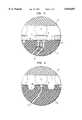
- FIG. 1shows a magnified view of a solder ball contact in typical relationship to an unmodified wire bonding contact.
- FIG. 2shows a magnified view of a solder ball contact in relationship to a conductive pad contact attached to a single embedded wire.
- FIG. 3shows a magnified view of a solder ball contact in relationship to a conductive pad contact attached to a two wire grouping.
- FIG. 4shows a magnified view of a solder ball contact in relationship to a polymer contact attached to a single embedded wire.
- FIG. 5shows a magnified view of a solder ball contact in relationship to a polymer contact attached to a two wire grouping.
- FIG. 6shows a magnified view of a solder ball contact in relationship to wire bonding contact leading from a two wire grouping which is surrounded by a thin layer of flexible polymer.
- FIG. 7shows an interconnector fixture using the interconnector of this invention.
- FIG. 8shows another interconnector fixture using the interconnector of this invention.
- FIG. 9shows an interconnector fixture for a connecting article having SBC type contacts.
- FIG. 10shows the application of gold plating to an area array on the substrate.
- FIG. 11shows the bonding of wires to the gold plated areas.
- FIG. 12shows the formation of laser balls on the bonded wires.
- FIG. 13shows the wires enclosed in a casting dam.
- FIG. 14shows the etching of the exposed substrate surface.
- FIG. 15shows the first interconnector assembly
- FIG. 16shows the second interconnector assembly
- FIG. 17shows a typical stamped substrate on the bonded wires.
- FIG. 18shows an expanded view of a stamped substrate.
- FIG. 19shows a magnified side view of the second substrate sub-assembly.
- FIG. 20shows the third interconnector assembly.
- FIG. 21shows a magnified side view of the third substrate sub-assembly.
- the present inventionprovides an improved electrical connecting device useable for interconnecting a module having high density type contacts with a printed circuit board or with another module.
- this inventionis a structure, to be referred henceforth as an interconnector, for the interconnection of a connecting article with a module having contacts preferably of the SBC type.
- the significance of the SBC interconnector contact area problemis observed by considering the illustration of FIG. 1.
- FIG. 1shows a magnified view of an SBC module 30 mated with an interconnector 10.
- the solder ball contact 32is shown in typical relationship to a heretofore typical elastomeric socket wire bonding contact 16 formed at an end of an embedded wire 17.
- the wire bonding contact 16is 1 to 10 mils in diameter.
- the irregular 20 to 40 mil diameter solder ball 32cannot make reliable or durable contact with the wire bonding contact 16.
- the inventorshave shown experimentally that enlarging and/or supporting the top surface area of the wire bonding contact 16 increases the durability and reliability of the interconnector 10.
- a means to achieve repeated, long term and reliable connectivityis to enlarge the top surface area of the wire bonding contact.
- Several alternative meansare herein described which provide the needed enlarged top surface area.
- a conductive contact pad 24 having a wide top-surface-area 13is attached to each wire bonding contact 16 on the interconnector top surface 23 of interconnector 10.
- the contact pad 24is attached to the wire bonding contact 16 along the pad's bottom surface 15.
- the pad's bottom surfaceis generally plated with a noble metal to enable formation of a low resistance attachment.
- the contact pad's 24 top surface area 13makes available to the solder ball a wide area of contact surface area.
- the top surface area 13is also generally plated. Compression of the solder ball contact 32 of an SBC module 30 against a contact pad 24 results in a reliable and durable electrical connection.
- a means to strengthen the interconnector mediumis to group two or more embedded wires for connection to a common contact pad 24.
- a two wire grouping 22is shown in FIG. 3.
- the grouping 22provides enhanced ability to the embedded wires to withstand the pressure resulting from a compressed connection of the solder ball 32 to the contact pad 24. It results in an increased strength and compliant connective medium.
- Combining three or more wires in a grouping for attachment to a common contact padfurther strengthens the connecting medium. In a three wire grouping the wires are best attached to the pad to form a triangle. In a four wire grouping the wires are preferably attached to the pads to form a square.
- FIG. 4A third alternative capable of providing connection of an SBC module to a circuit board and having enhanced durability is shown in FIG. 4.
- the conducting contact padis replaced with a polymer pad 28.
- Use of a polymer padenhances the overall compliance of the contact.
- the polymer pad 28is coated with a metal 13.
- the metal coating 13is attached to make electrical contact with an embedded wire 17.
- the metal coating 13is generally plated with a noble metal.
- a fourth embodimentcombines the attributes of the second and third embodiments by having the polymer pad 28 enclose two or more wire bonding contacts 16 to form a wire group 22 as shown in FIG. 5.
- the enclosed wire bonding contacts 16are all attached to make electrical contact with the common metal coating 13. This provides both a wide top end contact area for the solder ball contact 32 and also increases the strength, compliance and durability of the connecting medium which is a wire group 22 rather than an individual wire 17.
- FIG. 6shows a magnified view of another alternative means for an interconnector with enhanced durability. It uses a thin layer of flexible polymer 26 placed upon the top surface 23 of the interconnector 10. The polymer is made to surround and essentially captivate the wire bonding contacts. Increased strength results when the polymer surrounds and captivates together two or more wire bonding contacts.
- FIG. 6shows a two wire grouping.
- the wire bonding contact 16 on the end of the conductor wire 17should have its top surface exposed and is best placed to be flush with the polymer surface 27 of the layer of polymer 26.
- the exposed wire bonding contactshould be able to make direct electrical contact with the solder ball 32 on the SBC module 30.
- the thin layer of polymerdistributes the contact force from the solder balls 32 on the SBC module over a wider area of the polymer surface 26 thereby preventing excessive deformation of the wire grouping 22 in the dielectric material 21.
- the dielectric material 21is generally an elastomeric material.
- either or both ends of an embedded wiremay have an enlarged end.
- An enlarged endmay be attached to a single embedded wire or to a grouping means for grouping together a combination of at least two embedded members at the enlarged end.
- Thisis applicable when the grouping means is comprised of a conductive pad, or when the grouping means is comprised of a polymer pad which has a metallic coating which makes electrical contact with the enlarged end, especially when the coating is a metal selected from the group consisting of Au, Pd, Pt, or one of their alloys, or when an enlarged end extends to or through the body surface at a surface location wherein the grouping means is comprised of a polymer layer disposed over a body surface, and wherein the polymer layer has a hole corresponding to the surface location.
- the interconnectorincludes a fixture which can provide controlled connectivity of the SBC module to the connecting article. Therefore another object of the present invention is to provide a means to the connecting device to act as a clamping fixture so as to provide consistent pressure between the contacts of a module being interconnected, the interconnecting device and a connecting article.
- the fixtureshould include a means of aligning the corresponding contacts on the interconnecting device with the module contacts and also with the connecting article.
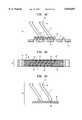
- FIG. 7shows an embodiment of such a fixture 40.
- the interconnector 10is held by a dam 20 in a position such that its lower laser ball contacts 25 are aligned with printed circuit board pads 61 on the connecting article 60.
- the SBC module 30is positioned such that its solder balls 32 are aligned with the contact pads 24.
- a top plate 55is placed over the SBC module 30. The entire assembly is held in place with fasteners 56 such as the nut and bolt shown in FIG. 6.
- FIG. 8shows improvements that can be made to the fixture 50. These include the use of a cushion 52 between the SBC module 30 and the top plate 55.
- the cushionis a polymer cushion 52 which is used to transfer the clamping force from the top plate 55 of the clamping fixture 50 to the top surface of the SBC module 30.
- Use of a controlled thickness spacer 54prevents over-compression of the solder ball contacts 32 with the connecting pads 24.
- the spacer 54should also have an alignment feature 53 for fine alignment of the SBC module 30.
- the fixture 40should also have a stiffener 51 placed between the fastener 56 and the connecting article 60. Use of a stiffener 51 prevents bowing of the connecting article 60.
- FIG. 9shows a modified interconnector 9 useable to connect with an article 65 having SBC type contacts 63 or other similar contacts.
- a second alignment feature 57could be used for aligning the interconnector article pads 64 with the connecting article solder balls 63.
- a second spacer 56could be used between the connecting article 65 and the enlarged first spacer 58.
- the second spacer 56could be made of an elastic polymer.
- the large pads 63could be either of polymer or of a metallic material.
- a desirable process to fabricate large polymer pads 63 on the interconnector's article connecting surfaceis the following.
- a metallic sheet prestamped with a pattern having holes centered around, matching and larger than the article surface laser board arrangementis formed and attached to the interconnector surface.
- the patterned hole openingsare filled partially or wholly with a polymer material.
- the structureis cured and the mask is removed either physically or by etching.
- the patterned holesare not filled wholly so as to leave room to spot or evaporate a desirable contact metallurgy over the laser ball and polymer surface before the mask is removed.
- FIG. 10shows the first step used to fabricate an interconnector assembly, such as the interconnector assembly 35 shown in FIG. 8, with conductive contact pads 24 for the fixture 40.
- a substrate 11, made of copper or other suitable conductive material,is fabricated with an area array of gold plated bottom surfaces 13 on the substrate bottom surface 12, and a correspondingly positioned area array of gold plated top surfaces 15 on the substrate top surface 14.
- Other noble metalsuch as Pt or Pd can be used for the substrate area array plating instead of gold.
- a barrier layeris typically used under the noble metal to prevent diffusion of the substrate to the surface.
- FIG. 11shows the next step of bonding the wire bonding contacts 16 of two bond wires 17.
- the bond wire 17is formed at an angle and cut to form a free standing structure with a straight end 18.
- FIG. 11shows two bonding wires 17 bonded to the gold plated top surface, the same process would be followed when bonding laser balls emanating from one, three or more bond wires to each gold plated top surface.
- FIG. 12shows the laser ball forming process at ends 18 of the angled bond wires 17 to create ball shaped contacts 19.
- the size of a ball shaped contact 19 on the end of the angled bond wires 17is controlled by the laser power density and the alignment of the focal point from the end 18 of the wire.
- the resulting array of angled bond wires 17forms the first substrate sub-assembly 8 upon which a casting dam 20 is placed.
- a casting dam 20is placed around the array of angled bond wires as shown in FIG. 13.
- the casting dam 20is used to contain an uncured dielectric material 21 until it is cured.
- the dielectricis usually a liquid elastomer.
- a controlled volume of dielectric material 21is dispensed into the cavity formed by the casting dam 20 such as to leave the ball shaped contacts 19 exposed.
- the dielectric materialis allowed to settle out before curing.
- the substrate 11is chemically etched as shown in FIG. 14.
- the etching processselectively removes the exposed unplated substrate on the substrate bottom surface 12 thereby leaving an array of individual conductive contact pads 24.
- the resulting first interconnector assembly 35is inverted as shown in FIG. 15.
- the interconnector assembly 35becomes an integral part of fixture 40, as shown in FIG. 7.
- FIG. 16shows a second interconnector assembly 36 resulting when using polymer pads of the type illustrated in FIG. 5.
- a process to form the polymer padsincludes the following steps.
- a conductive substrateusually a copper substrate, is prestamped with the desired shape and dimensions.
- FIG. 17shows such a typical substrate 70 in relation to a substrate carrier 71.
- the stampingis such as to form a crater 72 in the substrate 70 at each point where it is desired to locate a polymer pad.
- An expanded view of the stamped substrate for a 13 by 11 pad arrayis shown in FIG. 18.
- the substrate 70is thus capable of having up to 143 pads.
- FIG. 19shows a magnified portion of a side view of the stamped substrate 70 with craters 72.
- the craters 72generally have fixed pitch and height.
- Wires 17, having thermionic wire bonds 16 at one end,are put down at the bottom 74 of a crater 72 as shown in FIG. 19.
- the wiresare formed at an angle and cut to form a free standing structure with a straight end 18.
- a laser ball 19is formed at the straight end 18 of each wire.
- a polymer 76is poured into each crater 72 so as to cover the wire bond 16, but not to reach the top of the crater 77.
- the polymermay be epoxy, polyimide or others known to those skilled in the art.
- the polymeris fully cured thereby forming a hard and large polymer pad.
- the resulting array of angled bond wires 17forms the second substrate sub-assembly 75 upon which a casting dam 20 is placed.
- the second interconnector 36can be formed by placing a casting dam 20 around the array of angled bond wires 17 of second substrate sub-assembly 75 in a similar fashion as was described for the embodiment shown in FIG. 13.
- the casting dam 20, shown inverted in FIG. 16is used to contain an uncured dielectric material 21, usually an elastomeric solution, until it is cured.
- a controlled volume of dielectric material 21is dispensed into the cavity formed by the casting dam 20 such as to leave the ball shaped contacts 19 exposed. The dielectric material is allowed to settle out before curing. Once the dielectric has cured, the substrate 70 is chemically etched.
- the etching processis such as to selectively remove the substrate crater walls 78 so as to leave an array of individual metallic covered polymer pads 28.
- the metallic cover 29is generally plated with a noble metal. The plating serves as the contact interface with the solder ball 32 on an SBC module.
- the spaces 34 between contact pads 28provides a means of mechanical decoupling from the adjacent contact pads and allows the contact pads 28 to compress independently for high compliance applications.
- the resulting second interconnector assembly 36is inverted to the configuration shown in FIG. 16.
- the second interconnector assembly 36can become an integral part of fixture 40 replacing first interconnector 35 in FIG. 7, and an integral part of fixture 45 replacing first interconnector 35 in FIG. 8.
- FIG. 20shows a third interconnector assembly 37 resulting when the technique shown in FIG. 6 is used. It uses plated wire bonding contacts 16 to connect directly with the solder ball connections. The wire bonding contacts 16 are captivated in a flexible polymer 26. It is best to have the balls bonds 16 on the ends of the conductive wires 17 flush with the polymer top surface 29 of the thin layer of polymer 26 so as to provide a direct contact interface with the solder ball contacts of the SBC module.
- the third interconnector assembly 37can be formed by using a thin, essentially flat substrate 80 shown in FIG. 21. The substrate is marked correspondingly on both its flat surfaces to indicate the desired positions of the wire bonding contacts. Wires 17, having thermionic wire bonds 16 at one end, are put down according to the substrate marking. The wires are formed at an angle and cut to form a free standing structure with a straight end 18. A laser ball 19 is formed at the straight end 18 of each wire.
- the resulting array of angled bond wires 17forms the third substrate subassembly 79 upon which a casting dam 20 is placed.
- the third interconnector 37 shown in FIG. 20,is formed by placing a casting dam 20 around the array of angled bond wires 17, contained in the third substrate sub-assembly 79, in a similar fashion as was described for the embodiment shown in FIG. 13.
- the casting dam 20, shown inverted in FIG. 20,is used to receive a polymer 26 poured upon the substrate so as to enclose the wire bonding contacts 16.
- the polymermay be epoxy, polyimide or others known to those skilled in the art
- the polymeris fully cured thereby forming a thin polymer layer captivating the wire bonding contacts.
- a controlled volume of dielectric material 21is dispensed into the cavity on top of the polymer layer 26 such as to leave the ball shaped contacts 19 exposed.
- the dielectric materialusually an elastomeric solution, is allowed to settle out before curing.
- the substrate 62is chemically etched.
- the etching processis such as to remove the substrate so as to leave an array of exposed individual, or groupings of, wire bonding contacts 16.
- the wire bonding contacts 16are generally plated with a noble metal. The plating serves as the contact interface with the solder ball 32 on an SBC module.
- Encasing the wire bonding contacts 16 in the thin layer of polymer 28distributes the contact force from the solder balls 32 on the SBC module over a wider area on the top surface 27 of the interconnector socket 37 to prevent excessive deformation of the wire conductors 17 in the elastomer material 21.
- the resulting third interconnector assembly 37is inverted to the configuration shown in FIG. 17.
- the third interconnector assembly 37can become an integral part of fixture 40 replacing first interconnector 35 in FIG. 7, and an integral part of fixture 45 replacing first interconnector 35 in FIG. 8.
Landscapes
- Coupling Device And Connection With Printed Circuit (AREA)
- Connecting Device With Holders (AREA)
Abstract
Description
Claims (18)
Priority Applications (3)
| Application Number | Priority Date | Filing Date | Title |
|---|---|---|---|
| US08/527,733US5810607A (en) | 1995-09-13 | 1995-09-13 | Interconnector with contact pads having enhanced durability |
| US08/739,343US6286208B1 (en) | 1995-09-13 | 1996-10-28 | Interconnector with contact pads having enhanced durability |
| US10/145,661US20030048108A1 (en) | 1993-04-30 | 2002-05-14 | Structural design and processes to control probe position accuracy in a wafer test probe assembly |
Applications Claiming Priority (1)
| Application Number | Priority Date | Filing Date | Title |
|---|---|---|---|
| US08/527,733US5810607A (en) | 1995-09-13 | 1995-09-13 | Interconnector with contact pads having enhanced durability |
Related Child Applications (2)
| Application Number | Title | Priority Date | Filing Date |
|---|---|---|---|
| US08/739,343ContinuationUS6286208B1 (en) | 1993-04-30 | 1996-10-28 | Interconnector with contact pads having enhanced durability |
| US08/739,343DivisionUS6286208B1 (en) | 1993-04-30 | 1996-10-28 | Interconnector with contact pads having enhanced durability |
Publications (1)
| Publication Number | Publication Date |
|---|---|
| US5810607Atrue US5810607A (en) | 1998-09-22 |
Family
ID=24102712
Family Applications (2)
| Application Number | Title | Priority Date | Filing Date |
|---|---|---|---|
| US08/527,733Expired - LifetimeUS5810607A (en) | 1993-04-30 | 1995-09-13 | Interconnector with contact pads having enhanced durability |
| US08/739,343Expired - LifetimeUS6286208B1 (en) | 1993-04-30 | 1996-10-28 | Interconnector with contact pads having enhanced durability |
Family Applications After (1)
| Application Number | Title | Priority Date | Filing Date |
|---|---|---|---|
| US08/739,343Expired - LifetimeUS6286208B1 (en) | 1993-04-30 | 1996-10-28 | Interconnector with contact pads having enhanced durability |
Country Status (1)
| Country | Link |
|---|---|
| US (2) | US5810607A (en) |
Cited By (134)
| Publication number | Priority date | Publication date | Assignee | Title |
|---|---|---|---|---|
| US5947751A (en)* | 1998-04-03 | 1999-09-07 | Vlsi Technology, Inc. | Production and test socket for ball grid array semiconductor package |
| US6062879A (en)* | 1995-11-27 | 2000-05-16 | International Business Machines Corporation | High density test probe with rigid surface structure |
| US6097607A (en)* | 1996-11-01 | 2000-08-01 | Via, Inc. | Flexible computer system |
| US6097609A (en)* | 1998-12-30 | 2000-08-01 | Intel Corporation | Direct BGA socket |
| WO2000055946A1 (en)* | 1999-03-12 | 2000-09-21 | Motorola Inc. | System for providing a removable high density electrical interconnect for flexible circuits |
| WO2000056132A1 (en)* | 1999-03-17 | 2000-09-21 | Input/Output, Inc. | Low stress die attachment |
| US6162064A (en)* | 1997-10-27 | 2000-12-19 | Motorola | Method and apparatus for elastomer connection between a bonding shelf and a substrate |
| US6232147B1 (en)* | 1997-03-19 | 2001-05-15 | Fujitsu Limited | Method for manufacturing semiconductor device with pad structure |
| US6264476B1 (en) | 1999-12-09 | 2001-07-24 | High Connection Density, Inc. | Wire segment based interposer for high frequency electrical connection |
| SG82621A1 (en)* | 1998-10-30 | 2001-08-21 | St Assembly Test Services Ltd | Ball grid array tester socket |
| EP1094547A3 (en)* | 1999-10-19 | 2001-10-04 | Berg Electronics Manufacturing B.V. | Electrical connector with strain relief |
| US20010042639A1 (en)* | 1996-07-09 | 2001-11-22 | Takaaki Higashida | Semiconductor element-mounting board and semiconductor device |
| US6338629B1 (en)* | 1999-03-15 | 2002-01-15 | Aprion Digital Ltd. | Electrical connecting device |
| US6341963B1 (en)* | 2000-07-06 | 2002-01-29 | Advanced Micro Devices, Inc. | System level test socket |
| US6347947B1 (en)* | 2000-07-03 | 2002-02-19 | Advanced Interconnect Solutions | Method and apparatus for protecting and strengthening electrical contact interfaces |
| US6351392B1 (en) | 1999-10-05 | 2002-02-26 | Ironwood Electronics, Inc, | Offset array adapter |
| US6386890B1 (en) | 2001-03-12 | 2002-05-14 | International Business Machines Corporation | Printed circuit board to module mounting and interconnecting structure and method |
| US6392887B1 (en)* | 1999-12-14 | 2002-05-21 | Intel Corporation | PLGA-BGA socket using elastomer connectors |
| US6394819B1 (en) | 1998-10-29 | 2002-05-28 | The Whitaker Corporation | Dielectric member for absorbing thermal expansion and contraction at electrical interfaces |
| US6394820B1 (en) | 1999-10-14 | 2002-05-28 | Ironwood Electronics, Inc. | Packaged device adapter assembly and mounting apparatus |
| US6438831B1 (en)* | 1999-05-28 | 2002-08-27 | Tokyo Electron Limited | Method of manufacturing an interconnector |
| US6447308B1 (en)* | 2000-10-31 | 2002-09-10 | Paricon Technologies Corporation | Method and device for increasing elastomeric interconnection robustness |
| US6456100B1 (en)* | 1998-01-20 | 2002-09-24 | Micron Technology, Inc. | Apparatus for attaching to a semiconductor |
| US20020135388A1 (en)* | 1996-08-08 | 2002-09-26 | Gleason K. Reed | Membrane probing system with local contact scrub |
| US6528984B2 (en)* | 1996-09-13 | 2003-03-04 | Ibm Corporation | Integrated compliant probe for wafer level test and burn-in |
| US6533589B1 (en) | 1999-10-14 | 2003-03-18 | Ironwood Electronics, Inc. | Packaged device adapter assembly |
| US6540525B1 (en)* | 2001-08-17 | 2003-04-01 | High Connection Density, Inc. | High I/O stacked modules for integrated circuits |
| US6545226B2 (en)* | 2001-05-31 | 2003-04-08 | International Business Machines Corporation | Printed wiring board interposer sub-assembly |
| US6595784B2 (en) | 2001-05-15 | 2003-07-22 | International Business Machines Corporation | Interposer member having apertures for relieving stress and increasing contact compliancy |
| US20030166355A1 (en)* | 2002-01-09 | 2003-09-04 | Everett Simons | Apparatus for applying a mechanically-releasable balanced compressive load to a compliant anisotropic conductive elastomer electrical connector |
| US6638077B1 (en)* | 2001-02-26 | 2003-10-28 | High Connection Density, Inc. | Shielded carrier with components for land grid array connectors |
| US20030202768A1 (en)* | 2001-05-25 | 2003-10-30 | Steven Nasiri | High density optical fiber array |
| EP1376763A1 (en)* | 1999-10-19 | 2004-01-02 | Berg Electronics Manufacturing B.V. | Electrical connector with strain relief and method of securing an electrical connector to a substrate |
| US6695623B2 (en) | 2001-05-31 | 2004-02-24 | International Business Machines Corporation | Enhanced electrical/mechanical connection for electronic devices |
| US20040036162A1 (en)* | 2002-08-21 | 2004-02-26 | Shih-Fang Chuang | Integrated circuit package with heatsink support |
| US20040062015A1 (en)* | 2002-09-26 | 2004-04-01 | Yakov Belopolsky | Surface mounted electrical components |
| US6730541B2 (en)* | 1997-11-20 | 2004-05-04 | Texas Instruments Incorporated | Wafer-scale assembly of chip-size packages |
| US20040106307A1 (en)* | 2002-11-27 | 2004-06-03 | Akira Okitsu | Socket for electrical parts |
| US20040127071A1 (en)* | 1999-12-16 | 2004-07-01 | Weiss Roger E. | Pin-array, separable, compliant electrical contact member |
| US20040134676A1 (en)* | 2003-01-10 | 2004-07-15 | Shue Thomas L. | Cover for ball-grid array conenctor |
| US6776859B1 (en) | 2000-11-27 | 2004-08-17 | Saturn Electronics & Engineering, Inc. | Anisotropic bonding system and method using dynamic feedback |
| US20040192080A1 (en)* | 2003-03-24 | 2004-09-30 | Che-Yu Li | Electrical contact |
| US6805278B1 (en) | 1999-10-19 | 2004-10-19 | Fci America Technology, Inc. | Self-centering connector with hold down |
| US20040219807A1 (en)* | 2003-01-09 | 2004-11-04 | Weiss Roger E | Apparatus for applying a mechanically-releasable balanced compressive load to an assembly such as a complaint anisotropic conductive elastomer electrical connector |
| US20040232927A1 (en)* | 2002-05-23 | 2004-11-25 | Gleason K. Reed | Probe for testing a device under test |
| US20040242030A1 (en)* | 2003-05-30 | 2004-12-02 | Ironwood Electronics, Inc. | Packaged device adapter assembly with alignment structure and methods regarding same |
| US20040249825A1 (en)* | 2003-06-05 | 2004-12-09 | International Business Machines Corporation | Administering devices with dynamic action lists |
| US6846115B1 (en) | 2001-01-29 | 2005-01-25 | Jds Uniphase Corporation | Methods, apparatus, and systems of fiber optic modules, elastomeric connections, and retention mechanisms therefor |
| US20050048806A1 (en)* | 2003-03-24 | 2005-03-03 | Che-Yu Li | Electrical contact and connector and method of manufacture |
| US20050048807A1 (en)* | 2003-03-24 | 2005-03-03 | Che-Yu Li | Electrical contact and connector and method of manufacture |
| US6885106B1 (en)* | 2001-01-11 | 2005-04-26 | Tessera, Inc. | Stacked microelectronic assemblies and methods of making same |
| US20050090127A1 (en)* | 2003-10-23 | 2005-04-28 | Van Den Heede Peter I.A. | Device for connecting electric components |
| US20050196979A1 (en)* | 2004-03-02 | 2005-09-08 | Ironwood Electronics, Inc. | Adapter apparatus with conductive elements mounted using curable material and methods regarding same |
| US6948242B2 (en)* | 1998-08-17 | 2005-09-27 | Infineon Technologies Ag | Process for producing a contact-making device |
| US20060028220A1 (en)* | 2004-07-21 | 2006-02-09 | K&S Interconnect, Inc. | Reinforced probes for testing semiconductor devices |
| US7042241B2 (en) | 1997-06-10 | 2006-05-09 | Cascade Microtech, Inc. | Low-current pogo probe card |
| US7057404B2 (en) | 2003-05-23 | 2006-06-06 | Sharp Laboratories Of America, Inc. | Shielded probe for testing a device under test |
| US7071718B2 (en) | 1995-12-01 | 2006-07-04 | Gascade Microtech, Inc. | Low-current probe card |
| US7075320B2 (en) | 2002-11-13 | 2006-07-11 | Cascade Microtech, Inc. | Probe for combined signals |
| US7104804B2 (en)* | 2000-07-03 | 2006-09-12 | Advanced Interconnect Solutions | Method and apparatus for memory module circuit interconnection |
| US20060223362A1 (en)* | 2005-04-05 | 2006-10-05 | Swain Wilfred J | Electrical connector with cooling features |
| US7148711B2 (en) | 2000-02-25 | 2006-12-12 | Cascade Microtech, Inc. | Membrane probing system |
| US7178236B2 (en) | 1999-06-04 | 2007-02-20 | Cascade Microtech, Inc. | Method for constructing a membrane probe using a depression |
| US7233160B2 (en) | 2000-12-04 | 2007-06-19 | Cascade Microtech, Inc. | Wafer probe |
| US7266889B2 (en) | 1998-07-14 | 2007-09-11 | Cascade Microtech, Inc. | Membrane probing system |
| US7282945B1 (en)* | 1996-09-13 | 2007-10-16 | International Business Machines Corporation | Wafer scale high density probe assembly, apparatus for use thereof and methods of fabrication thereof |
| US7355420B2 (en) | 2001-08-21 | 2008-04-08 | Cascade Microtech, Inc. | Membrane probing system |
| US7368927B2 (en) | 2004-07-07 | 2008-05-06 | Cascade Microtech, Inc. | Probe head having a membrane suspended probe |
| US7368814B1 (en) | 2004-03-26 | 2008-05-06 | Ironwood Electronics, Inc. | Surface mount adapter apparatus and methods regarding same |
| US7384289B2 (en) | 2005-01-31 | 2008-06-10 | Fci Americas Technology, Inc. | Surface-mount connector |
| US7402064B2 (en) | 2003-12-31 | 2008-07-22 | Fci Americas Technology, Inc. | Electrical power contacts and connectors comprising same |
| US7403028B2 (en) | 2006-06-12 | 2008-07-22 | Cascade Microtech, Inc. | Test structure and probe for differential signals |
| US7420381B2 (en) | 2004-09-13 | 2008-09-02 | Cascade Microtech, Inc. | Double sided probing structures |
| US7425145B2 (en) | 2006-05-26 | 2008-09-16 | Fci Americas Technology, Inc. | Connectors and contacts for transmitting electrical power |
| US7427868B2 (en) | 2003-12-24 | 2008-09-23 | Cascade Microtech, Inc. | Active wafer probe |
| US7443186B2 (en) | 2006-06-12 | 2008-10-28 | Cascade Microtech, Inc. | On-wafer test structures for differential signals |
| US7449899B2 (en) | 2005-06-08 | 2008-11-11 | Cascade Microtech, Inc. | Probe for high frequency signals |
| US7458839B2 (en) | 2006-02-21 | 2008-12-02 | Fci Americas Technology, Inc. | Electrical connectors having power contacts with alignment and/or restraining features |
| US7476108B2 (en) | 2004-12-22 | 2009-01-13 | Fci Americas Technology, Inc. | Electrical power connectors with cooling features |
| US7504842B2 (en) | 1997-05-28 | 2009-03-17 | Cascade Microtech, Inc. | Probe holder for testing of a test device |
| US20090102041A1 (en)* | 2007-10-17 | 2009-04-23 | Ted Ju | Electrical connection device and assembly method thereof |
| US7535247B2 (en) | 2005-01-31 | 2009-05-19 | Cascade Microtech, Inc. | Interface for testing semiconductors |
| US20090174423A1 (en)* | 2004-07-21 | 2009-07-09 | Klaerner Peter J | Bond Reinforcement Layer for Probe Test Cards |
| US7609077B2 (en) | 2006-06-09 | 2009-10-27 | Cascade Microtech, Inc. | Differential signal probe with integral balun |
| US7619419B2 (en) | 2005-06-13 | 2009-11-17 | Cascade Microtech, Inc. | Wideband active-passive differential signal probe |
| USD606497S1 (en) | 2009-01-16 | 2009-12-22 | Fci Americas Technology, Inc. | Vertical electrical connector |
| USD606496S1 (en) | 2009-01-16 | 2009-12-22 | Fci Americas Technology, Inc. | Right-angle electrical connector |
| US7641500B2 (en) | 2007-04-04 | 2010-01-05 | Fci Americas Technology, Inc. | Power cable connector system |
| USD608293S1 (en) | 2009-01-16 | 2010-01-19 | Fci Americas Technology, Inc. | Vertical electrical connector |
| US7656172B2 (en) | 2005-01-31 | 2010-02-02 | Cascade Microtech, Inc. | System for testing semiconductors |
| USD610548S1 (en) | 2009-01-16 | 2010-02-23 | Fci Americas Technology, Inc. | Right-angle electrical connector |
| USRE41283E1 (en) | 2003-01-28 | 2010-04-27 | Fci Americas Technology, Inc. | Power connector with safety feature |
| US7723999B2 (en) | 2006-06-12 | 2010-05-25 | Cascade Microtech, Inc. | Calibration structures for differential signal probing |
| US7726982B2 (en) | 2006-06-15 | 2010-06-01 | Fci Americas Technology, Inc. | Electrical connectors with air-circulation features |
| USD618181S1 (en) | 2009-04-03 | 2010-06-22 | Fci Americas Technology, Inc. | Asymmetrical electrical connector |
| USD618180S1 (en) | 2009-04-03 | 2010-06-22 | Fci Americas Technology, Inc. | Asymmetrical electrical connector |
| USD619099S1 (en) | 2009-01-30 | 2010-07-06 | Fci Americas Technology, Inc. | Electrical connector |
| US7764072B2 (en) | 2006-06-12 | 2010-07-27 | Cascade Microtech, Inc. | Differential signal probing system |
| US7762857B2 (en) | 2007-10-01 | 2010-07-27 | Fci Americas Technology, Inc. | Power connectors with contact-retention features |
| US20100216321A1 (en)* | 2009-02-26 | 2010-08-26 | Ironwood Electronics, Inc. | Adapter apparatus with sleeve spring contacts |
| US7876114B2 (en) | 2007-08-08 | 2011-01-25 | Cascade Microtech, Inc. | Differential waveguide probe |
| US7888957B2 (en) | 2008-10-06 | 2011-02-15 | Cascade Microtech, Inc. | Probing apparatus with impedance optimized interface |
| US7905731B2 (en) | 2007-05-21 | 2011-03-15 | Fci Americas Technology, Inc. | Electrical connector with stress-distribution features |
| USD640637S1 (en) | 2009-01-16 | 2011-06-28 | Fci Americas Technology Llc | Vertical electrical connector |
| US8062051B2 (en) | 2008-07-29 | 2011-11-22 | Fci Americas Technology Llc | Electrical communication system having latching and strain relief features |
| USD664096S1 (en) | 2009-01-16 | 2012-07-24 | Fci Americas Technology Llc | Vertical electrical connector |
| US20120302095A1 (en)* | 2011-04-25 | 2012-11-29 | Apple Inc. | Interposer connectors |
| US8323049B2 (en) | 2009-01-30 | 2012-12-04 | Fci Americas Technology Llc | Electrical connector having power contacts |
| US20130052839A1 (en)* | 2011-08-30 | 2013-02-28 | Denso Corporation | Detachable connection structure |
| US8410806B2 (en) | 2008-11-21 | 2013-04-02 | Cascade Microtech, Inc. | Replaceable coupon for a probing apparatus |
| US20130335936A1 (en)* | 2011-05-12 | 2013-12-19 | Fujikura Ltd. | Interposer substrate, electronic device package, and electronic component |
| US20140167243A1 (en)* | 2012-12-13 | 2014-06-19 | Yuci Shen | Semiconductor packages using a chip constraint means |
| USD718253S1 (en) | 2012-04-13 | 2014-11-25 | Fci Americas Technology Llc | Electrical cable connector |
| US8905651B2 (en) | 2012-01-31 | 2014-12-09 | Fci | Dismountable optical coupling device |
| US20140370727A1 (en)* | 2013-06-12 | 2014-12-18 | Ironwood Electronics, Inc. | Adapter apparatus with suspended conductive elastomer interconnect |
| USD720698S1 (en) | 2013-03-15 | 2015-01-06 | Fci Americas Technology Llc | Electrical cable connector |
| US8944831B2 (en) | 2012-04-13 | 2015-02-03 | Fci Americas Technology Llc | Electrical connector having ribbed ground plate with engagement members |
| USD727268S1 (en) | 2012-04-13 | 2015-04-21 | Fci Americas Technology Llc | Vertical electrical connector |
| USD727852S1 (en) | 2012-04-13 | 2015-04-28 | Fci Americas Technology Llc | Ground shield for a right angle electrical connector |
| US9048583B2 (en) | 2009-03-19 | 2015-06-02 | Fci Americas Technology Llc | Electrical connector having ribbed ground plate |
| US9048565B2 (en) | 2013-06-12 | 2015-06-02 | Ironwood Electronics, Inc. | Adapter apparatus with deflectable element socket contacts |
| USD733662S1 (en) | 2013-01-25 | 2015-07-07 | Fci Americas Technology Llc | Connector housing for electrical connector |
| TWI491897B (en)* | 2013-01-03 | 2015-07-11 | 矽品精密工業股份有限公司 | Testing apparatus and testing method for semiconductor element |
| USD746236S1 (en) | 2012-07-11 | 2015-12-29 | Fci Americas Technology Llc | Electrical connector housing |
| US9257778B2 (en) | 2012-04-13 | 2016-02-09 | Fci Americas Technology | High speed electrical connector |
| US9474156B2 (en) | 2011-02-10 | 2016-10-18 | Apple Inc. | Interposer connectors with alignment features |
| US20170005427A1 (en)* | 2014-04-18 | 2017-01-05 | Yazaki Corporation | Conductive elastic member and connector |
| US9543703B2 (en) | 2012-07-11 | 2017-01-10 | Fci Americas Technology Llc | Electrical connector with reduced stack height |
| US20170365545A1 (en)* | 2016-06-21 | 2017-12-21 | Fujitsu Limited | Resin board, method of manufacturing resin board, circuit board, and method of manufacturing circuit board |
| US9853383B2 (en)* | 2015-09-11 | 2017-12-26 | General Electric Company | Conductive polymer contacts for surface mount technology connectors |
| US9877404B1 (en) | 2017-01-27 | 2018-01-23 | Ironwood Electronics, Inc. | Adapter apparatus with socket contacts held in openings by holding structures |
| JP2018529932A (en)* | 2015-07-03 | 2018-10-11 | オキンス エレクトロニクス カンパニー リミテッド | Test socket, test socket manufacturing method, and test socket jig assembly |
| US10122139B1 (en) | 2017-12-07 | 2018-11-06 | Ironwood Electronics, Inc. | Adapter apparatus with conductive elements mounted using laminate layer and methods regarding same |
| US20210343622A1 (en)* | 2018-09-27 | 2021-11-04 | Taiwan Semiconductor Manufacturing Company, Ltd. | Package structures and methods of manufacturing the same |
Families Citing this family (25)
| Publication number | Priority date | Publication date | Assignee | Title |
|---|---|---|---|---|
| US6580611B1 (en)* | 2001-12-21 | 2003-06-17 | Intel Corporation | Dual-sided heat removal system |
| US6590772B1 (en)* | 2002-04-17 | 2003-07-08 | Ted Ju | CPU and circuit board mounting arrangement |
| US7170306B2 (en)* | 2003-03-12 | 2007-01-30 | Celerity Research, Inc. | Connecting a probe card and an interposer using a compliant connector |
| US6924654B2 (en)* | 2003-03-12 | 2005-08-02 | Celerity Research, Inc. | Structures for testing circuits and methods for fabricating the structures |
| US6946859B2 (en) | 2003-03-12 | 2005-09-20 | Celerity Research, Inc. | Probe structures using clamped substrates with compliant interconnectors |
| US20040180561A1 (en)* | 2003-03-12 | 2004-09-16 | Nexcleon, Inc. | Structures for testing circuits and methods for fabricating the structures |
| US20040177995A1 (en)* | 2003-03-12 | 2004-09-16 | Nexcleon, Inc. | Structures for testing circuits and methods for fabricating the structures |
| US20040188811A1 (en)* | 2003-03-24 | 2004-09-30 | Intel Corporation | Circuit package apparatus, systems, and methods |
| JPWO2005029584A1 (en)* | 2003-09-22 | 2006-11-30 | 松下電器産業株式会社 | Semiconductor integrated circuit |
| US7245022B2 (en)* | 2003-11-25 | 2007-07-17 | International Business Machines Corporation | Semiconductor module with improved interposer structure and method for forming the same |
| US6888360B1 (en)* | 2004-02-20 | 2005-05-03 | Research In Motion Limited | Surface mount technology evaluation board having varied board pad characteristics |
| US7172431B2 (en)* | 2004-08-27 | 2007-02-06 | International Business Machines Corporation | Electrical connector design and contact geometry and method of use thereof and methods of fabrication thereof |
| TWI255466B (en)* | 2004-10-08 | 2006-05-21 | Ind Tech Res Inst | Polymer-matrix conductive film and method for fabricating the same |
| NL1027450C2 (en)* | 2004-11-09 | 2006-05-10 | Shin Etsu Polymer Europ B V | Interconnection connector, frame comprising such a connector, electrical measuring and testing device and contacting method with the aid of such a connector. |
| CN101288205B (en)* | 2004-12-16 | 2011-09-21 | 国际商业机器公司 | Metallized Elastomer Electrical Contacts |
| US7771208B2 (en) | 2004-12-16 | 2010-08-10 | International Business Machines Corporation | Metalized elastomeric electrical contacts |
| US7473102B2 (en)* | 2006-03-31 | 2009-01-06 | International Business Machines Corporation | Space transforming land grid array interposers |
| US8832936B2 (en)* | 2007-04-30 | 2014-09-16 | International Business Machines Corporation | Method of forming metallized elastomeric electrical contacts |
| WO2009134823A2 (en)* | 2008-05-01 | 2009-11-05 | 3M Innovative Properties Company | Stretchable conductive connector |
| US8700118B2 (en)* | 2008-05-01 | 2014-04-15 | 3M Innovative Properties Company | Biomedical sensor system |
| TW201106540A (en)* | 2009-08-04 | 2011-02-16 | Hon Hai Prec Ind Co Ltd | Electrical connection device |
| US8587132B2 (en)* | 2012-02-21 | 2013-11-19 | Broadcom Corporation | Semiconductor package including an organic substrate and interposer having through-semiconductor vias |
| US9093766B2 (en)* | 2013-09-25 | 2015-07-28 | Ford Global Technologies, Llc | Conductive ink elastomeric molded connector |
| KR101785428B1 (en) | 2016-04-21 | 2017-10-16 | (주) 마이크로프랜드 | Test Socket of Semiconductor Device |
| US9947634B1 (en)* | 2017-06-13 | 2018-04-17 | Northrop Grumman Systems Corporation | Robust mezzanine BGA connector |
Citations (34)
| Publication number | Priority date | Publication date | Assignee | Title |
|---|---|---|---|---|
| US2961746A (en)* | 1956-06-18 | 1960-11-29 | Aladdin Ind Inc | Printed circuits |
| US3430338A (en)* | 1964-08-11 | 1969-03-04 | Gen Motors Corp | Making a welded circuit assembly |
| US3541222A (en)* | 1969-01-13 | 1970-11-17 | Bunker Ramo | Connector screen for interconnecting adjacent surfaces of laminar circuits and method of making |
| US3557446A (en)* | 1968-12-16 | 1971-01-26 | Western Electric Co | Method of forming printed circuit board through-connections |
| US3795037A (en)* | 1970-05-05 | 1974-03-05 | Int Computers Ltd | Electrical connector devices |
| US3862790A (en)* | 1971-07-22 | 1975-01-28 | Plessey Handel Investment Ag | Electrical interconnectors and connector assemblies |
| US3889363A (en)* | 1971-02-16 | 1975-06-17 | Richard P Davis | Method of making printed circuit boards |
| US3954317A (en)* | 1974-02-27 | 1976-05-04 | Amp Incorporated | Elastomeric connector and its method of manufacture |
| US4003621A (en)* | 1975-06-16 | 1977-01-18 | Technical Wire Products, Inc. | Electrical connector employing conductive rectilinear elements |
| US4008300A (en)* | 1974-10-15 | 1977-02-15 | A & P Products Incorporated | Multi-conductor element and method of making same |
| US4295700A (en)* | 1978-10-12 | 1981-10-20 | Shin-Etsu Polymer Co., Ltd. | Interconnectors |
| US4329780A (en)* | 1978-09-28 | 1982-05-18 | Dayco Corporation | Method of making a reinforced wear-resistant liner |
| US4355199A (en)* | 1975-10-10 | 1982-10-19 | Luc Penelope Jane Vesey | Conductive connections |
| US4408814A (en)* | 1980-08-22 | 1983-10-11 | Shin-Etsu Polymer Co., Ltd. | Electric connector of press-contact holding type |
| US4509099A (en)* | 1980-02-19 | 1985-04-02 | Sharp Kabushiki Kaisha | Electronic component with plurality of terminals thereon |
| US4520562A (en)* | 1979-11-20 | 1985-06-04 | Shin-Etsu Polymer Co., Ltd. | Method for manufacturing an elastic composite body with metal wires embedded therein |
| US4548451A (en)* | 1984-04-27 | 1985-10-22 | International Business Machines Corporation | Pinless connector interposer and method for making the same |
| US4555523A (en)* | 1984-06-04 | 1985-11-26 | E. R. Squibb & Sons, Inc. | 7-Oxabicycloheptane substituted thio prostaglandin analogs and their use in the treatment of thrombolytic disease |
| US4575166A (en)* | 1984-05-01 | 1986-03-11 | International Business Machines Corp. | Circuitry on mylar and dual durometer rubber multiple connector |
| US4577918A (en)* | 1984-05-01 | 1986-03-25 | International Business Machines Corporation | Copper and dual durometer rubber multiple connector |
| US4778950A (en)* | 1985-07-22 | 1988-10-18 | Digital Equipment Corporation | Anisotropic elastomeric interconnecting system |
| US4793814A (en)* | 1986-07-21 | 1988-12-27 | Rogers Corporation | Electrical circuit board interconnect |
| US4820376A (en)* | 1987-11-05 | 1989-04-11 | American Telephone And Telegraph Company At&T Bell Laboratories | Fabrication of CPI layers |
| US4820170A (en)* | 1984-12-20 | 1989-04-11 | Amp Incorporated | Layered elastomeric connector and process for its manufacture |
| US4832609A (en)* | 1987-11-27 | 1989-05-23 | Eastman Kodak Company | Solderless circuit connection for bowed circuit board |
| US4991290A (en)* | 1988-07-21 | 1991-02-12 | Microelectronics And Computer Technology | Flexible electrical interconnect and method of making |
| US4998885A (en)* | 1989-10-27 | 1991-03-12 | International Business Machines Corporation | Elastomeric area array interposer |
| US5037312A (en)* | 1990-11-15 | 1991-08-06 | Amp Incorporated | Conductive gel area array connector |
| US5049084A (en)* | 1989-12-05 | 1991-09-17 | Rogers Corporation | Electrical circuit board interconnect |
| US5099309A (en)* | 1990-04-30 | 1992-03-24 | International Business Machines Corporation | Three-dimensional memory card structure with internal direct chip attachment |
| US5371654A (en)* | 1992-10-19 | 1994-12-06 | International Business Machines Corporation | Three dimensional high performance interconnection package |
| US5413489A (en)* | 1993-04-27 | 1995-05-09 | Aptix Corporation | Integrated socket and IC package assembly |
| US5518410A (en)* | 1993-05-24 | 1996-05-21 | Enplas Corporation | Contact pin device for IC sockets |
| US5611696A (en)* | 1994-12-14 | 1997-03-18 | International Business Machines Corporation | High density and high current capacity pad-to-pad connector comprising of spring connector elements (SCE) |
Family Cites Families (9)
| Publication number | Priority date | Publication date | Assignee | Title |
|---|---|---|---|---|
| US4636018A (en)* | 1985-06-05 | 1987-01-13 | Amp Incorporated | Elastomeric electrical connector |
| US5917707A (en)* | 1993-11-16 | 1999-06-29 | Formfactor, Inc. | Flexible contact structure with an electrically conductive shell |
| US4667129A (en)* | 1986-04-21 | 1987-05-19 | Jacques Papillon | Method and device for automatically switching on and off the headlights of a motor vehicle |
| US5098305A (en)* | 1987-05-21 | 1992-03-24 | Cray Research, Inc. | Memory metal electrical connector |
| US5061192A (en)* | 1990-12-17 | 1991-10-29 | International Business Machines Corporation | High density connector |
| US5355283A (en)* | 1993-04-14 | 1994-10-11 | Amkor Electronics, Inc. | Ball grid array with via interconnection |
| US5772451A (en)* | 1993-11-16 | 1998-06-30 | Form Factor, Inc. | Sockets for electronic components and methods of connecting to electronic components |
| US5764486A (en)* | 1996-10-10 | 1998-06-09 | Hewlett Packard Company | Cost effective structure and method for interconnecting a flip chip with a substrate |
| US6078500A (en)* | 1998-05-12 | 2000-06-20 | International Business Machines Inc. | Pluggable chip scale package |
- 1995
- 1995-09-13USUS08/527,733patent/US5810607A/ennot_activeExpired - Lifetime
- 1996
- 1996-10-28USUS08/739,343patent/US6286208B1/ennot_activeExpired - Lifetime
Patent Citations (35)
| Publication number | Priority date | Publication date | Assignee | Title |
|---|---|---|---|---|
| US2961746A (en)* | 1956-06-18 | 1960-11-29 | Aladdin Ind Inc | Printed circuits |
| US3430338A (en)* | 1964-08-11 | 1969-03-04 | Gen Motors Corp | Making a welded circuit assembly |
| US3557446A (en)* | 1968-12-16 | 1971-01-26 | Western Electric Co | Method of forming printed circuit board through-connections |
| US3541222A (en)* | 1969-01-13 | 1970-11-17 | Bunker Ramo | Connector screen for interconnecting adjacent surfaces of laminar circuits and method of making |
| US3795037A (en)* | 1970-05-05 | 1974-03-05 | Int Computers Ltd | Electrical connector devices |
| US3889363A (en)* | 1971-02-16 | 1975-06-17 | Richard P Davis | Method of making printed circuit boards |
| US3862790A (en)* | 1971-07-22 | 1975-01-28 | Plessey Handel Investment Ag | Electrical interconnectors and connector assemblies |
| US3954317A (en)* | 1974-02-27 | 1976-05-04 | Amp Incorporated | Elastomeric connector and its method of manufacture |
| US4008300A (en)* | 1974-10-15 | 1977-02-15 | A & P Products Incorporated | Multi-conductor element and method of making same |
| US4003621A (en)* | 1975-06-16 | 1977-01-18 | Technical Wire Products, Inc. | Electrical connector employing conductive rectilinear elements |
| US4355199A (en)* | 1975-10-10 | 1982-10-19 | Luc Penelope Jane Vesey | Conductive connections |
| US4329780A (en)* | 1978-09-28 | 1982-05-18 | Dayco Corporation | Method of making a reinforced wear-resistant liner |
| US4295700A (en)* | 1978-10-12 | 1981-10-20 | Shin-Etsu Polymer Co., Ltd. | Interconnectors |
| US4402562A (en)* | 1978-10-12 | 1983-09-06 | Shin-Etsu Polymer Co., Ltd. | Interconnectors |
| US4520562A (en)* | 1979-11-20 | 1985-06-04 | Shin-Etsu Polymer Co., Ltd. | Method for manufacturing an elastic composite body with metal wires embedded therein |
| US4509099A (en)* | 1980-02-19 | 1985-04-02 | Sharp Kabushiki Kaisha | Electronic component with plurality of terminals thereon |
| US4408814A (en)* | 1980-08-22 | 1983-10-11 | Shin-Etsu Polymer Co., Ltd. | Electric connector of press-contact holding type |
| US4548451A (en)* | 1984-04-27 | 1985-10-22 | International Business Machines Corporation | Pinless connector interposer and method for making the same |
| US4575166A (en)* | 1984-05-01 | 1986-03-11 | International Business Machines Corp. | Circuitry on mylar and dual durometer rubber multiple connector |
| US4577918A (en)* | 1984-05-01 | 1986-03-25 | International Business Machines Corporation | Copper and dual durometer rubber multiple connector |
| US4555523A (en)* | 1984-06-04 | 1985-11-26 | E. R. Squibb & Sons, Inc. | 7-Oxabicycloheptane substituted thio prostaglandin analogs and their use in the treatment of thrombolytic disease |
| US4820170A (en)* | 1984-12-20 | 1989-04-11 | Amp Incorporated | Layered elastomeric connector and process for its manufacture |
| US4778950A (en)* | 1985-07-22 | 1988-10-18 | Digital Equipment Corporation | Anisotropic elastomeric interconnecting system |
| US4793814A (en)* | 1986-07-21 | 1988-12-27 | Rogers Corporation | Electrical circuit board interconnect |
| US4820376A (en)* | 1987-11-05 | 1989-04-11 | American Telephone And Telegraph Company At&T Bell Laboratories | Fabrication of CPI layers |
| US4832609A (en)* | 1987-11-27 | 1989-05-23 | Eastman Kodak Company | Solderless circuit connection for bowed circuit board |
| US4991290A (en)* | 1988-07-21 | 1991-02-12 | Microelectronics And Computer Technology | Flexible electrical interconnect and method of making |
| US4998885A (en)* | 1989-10-27 | 1991-03-12 | International Business Machines Corporation | Elastomeric area array interposer |
| US5049084A (en)* | 1989-12-05 | 1991-09-17 | Rogers Corporation | Electrical circuit board interconnect |
| US5099309A (en)* | 1990-04-30 | 1992-03-24 | International Business Machines Corporation | Three-dimensional memory card structure with internal direct chip attachment |
| US5037312A (en)* | 1990-11-15 | 1991-08-06 | Amp Incorporated | Conductive gel area array connector |
| US5371654A (en)* | 1992-10-19 | 1994-12-06 | International Business Machines Corporation | Three dimensional high performance interconnection package |
| US5413489A (en)* | 1993-04-27 | 1995-05-09 | Aptix Corporation | Integrated socket and IC package assembly |
| US5518410A (en)* | 1993-05-24 | 1996-05-21 | Enplas Corporation | Contact pin device for IC sockets |
| US5611696A (en)* | 1994-12-14 | 1997-03-18 | International Business Machines Corporation | High density and high current capacity pad-to-pad connector comprising of spring connector elements (SCE) |
Non-Patent Citations (8)
| Title |
|---|
| "Elastomeric Interposer Using Film-Supported Metal Conductors" Disclosed Anonymously--Research Disclosure, Apr. 1991, No. 324, K. Mason Publications, Ltd., England. |
| "Elastomeric Interposer Using Wires in Elastomer Pad with Controlled Compliance" Disclosed Anonymounsly, Research Disclosure, Apr. 1991, No. 324,K. Mason Pub.Ltd.Eng. |
| "High Density Area Array Connector" Disclosed Anonymously, Research Disclosure, Apr. 1991, No. 324, K. Mason Publications Ltd., England. |
| "Shaped Elastomeric Interposer for Large Area Array Connectors", Disclosed Anonymously, Research Disclosure, Apr. 1991, No. 324, K. Mason Publications, Ltd., England. |
| Elastomeric Interposer Using Film Supported Metal Conductors Disclosed Anonymously Research Disclosure, Apr. 1991, No. 324, K. Mason Publications, Ltd., England.* |
| Elastomeric Interposer Using Wires in Elastomer Pad with Controlled Compliance Disclosed Anonymounsly, Research Disclosure, Apr. 1991, No. 324,K. Mason Pub.Ltd.Eng.* |
| High Density Area Array Connector Disclosed Anonymously, Research Disclosure, Apr. 1991, No. 324, K. Mason Publications Ltd., England.* |
| Shaped Elastomeric Interposer for Large Area Array Connectors , Disclosed Anonymously, Research Disclosure, Apr. 1991, No. 324, K. Mason Publications, Ltd., England.* |
Cited By (244)
| Publication number | Priority date | Publication date | Assignee | Title |
|---|---|---|---|---|
| US6062879A (en)* | 1995-11-27 | 2000-05-16 | International Business Machines Corporation | High density test probe with rigid surface structure |
| US7071718B2 (en) | 1995-12-01 | 2006-07-04 | Gascade Microtech, Inc. | Low-current probe card |
| US20010042639A1 (en)* | 1996-07-09 | 2001-11-22 | Takaaki Higashida | Semiconductor element-mounting board and semiconductor device |
| US20040158979A1 (en)* | 1996-07-09 | 2004-08-19 | Takaaki Higashida | Method of manufacturing a semiconductor element-mounting board |
| US7036221B2 (en) | 1996-07-09 | 2006-05-02 | Matsushita Electric Industrial Co., Ltd. | Method of manufacturing a semiconductor element-mounting board |
| US7541821B2 (en) | 1996-08-08 | 2009-06-02 | Cascade Microtech, Inc. | Membrane probing system with local contact scrub |
| US7109731B2 (en) | 1996-08-08 | 2006-09-19 | Cascade Microtech, Inc. | Membrane probing system with local contact scrub |
| US20020135388A1 (en)* | 1996-08-08 | 2002-09-26 | Gleason K. Reed | Membrane probing system with local contact scrub |
| US6927585B2 (en) | 1996-08-08 | 2005-08-09 | Cascade Microtech, Inc. | Membrane probing system with local contact scrub |
| US7893704B2 (en) | 1996-08-08 | 2011-02-22 | Cascade Microtech, Inc. | Membrane probing structure with laterally scrubbing contacts |
| US6528984B2 (en)* | 1996-09-13 | 2003-03-04 | Ibm Corporation | Integrated compliant probe for wafer level test and burn-in |
| US7282945B1 (en)* | 1996-09-13 | 2007-10-16 | International Business Machines Corporation | Wafer scale high density probe assembly, apparatus for use thereof and methods of fabrication thereof |
| US6097607A (en)* | 1996-11-01 | 2000-08-01 | Via, Inc. | Flexible computer system |
| US6232147B1 (en)* | 1997-03-19 | 2001-05-15 | Fujitsu Limited | Method for manufacturing semiconductor device with pad structure |
| US7504842B2 (en) | 1997-05-28 | 2009-03-17 | Cascade Microtech, Inc. | Probe holder for testing of a test device |
| US7068057B2 (en) | 1997-06-10 | 2006-06-27 | Cascade Microtech, Inc. | Low-current pogo probe card |
| US7042241B2 (en) | 1997-06-10 | 2006-05-09 | Cascade Microtech, Inc. | Low-current pogo probe card |
| US7148714B2 (en) | 1997-06-10 | 2006-12-12 | Cascade Microtech, Inc. | POGO probe card for low current measurements |
| US6162064A (en)* | 1997-10-27 | 2000-12-19 | Motorola | Method and apparatus for elastomer connection between a bonding shelf and a substrate |
| US6730541B2 (en)* | 1997-11-20 | 2004-05-04 | Texas Instruments Incorporated | Wafer-scale assembly of chip-size packages |
| US6939145B2 (en) | 1998-01-20 | 2005-09-06 | Micron Technology, Inc. | Spring element for use in an apparatus for attaching to a semiconductor and a method of making |
| US20050191876A1 (en)* | 1998-01-20 | 2005-09-01 | Hembree David R. | Spring element for use in an apparatus for attaching to a semiconductor and a method of making |
| US6598290B2 (en) | 1998-01-20 | 2003-07-29 | Micron Technology, Inc. | Method of making a spring element for use in an apparatus for attaching to a semiconductor |
| US7011532B2 (en) | 1998-01-20 | 2006-03-14 | Micron Technology, Inc. | Spring element for use in an apparatus for attaching to a semiconductor and a method of making |
| US6806493B1 (en) | 1998-01-20 | 2004-10-19 | Micron Technology, Inc. | Spring element for use in an apparatus for attaching to a semiconductor and a method of attaching |
| US6456100B1 (en)* | 1998-01-20 | 2002-09-24 | Micron Technology, Inc. | Apparatus for attaching to a semiconductor |
| US5947751A (en)* | 1998-04-03 | 1999-09-07 | Vlsi Technology, Inc. | Production and test socket for ball grid array semiconductor package |
| US7400155B2 (en) | 1998-07-14 | 2008-07-15 | Cascade Microtech, Inc. | Membrane probing system |
| US7761986B2 (en) | 1998-07-14 | 2010-07-27 | Cascade Microtech, Inc. | Membrane probing method using improved contact |
| US7266889B2 (en) | 1998-07-14 | 2007-09-11 | Cascade Microtech, Inc. | Membrane probing system |
| US8451017B2 (en) | 1998-07-14 | 2013-05-28 | Cascade Microtech, Inc. | Membrane probing method using improved contact |
| US7681312B2 (en) | 1998-07-14 | 2010-03-23 | Cascade Microtech, Inc. | Membrane probing system |
| US6948242B2 (en)* | 1998-08-17 | 2005-09-27 | Infineon Technologies Ag | Process for producing a contact-making device |
| US6394819B1 (en) | 1998-10-29 | 2002-05-28 | The Whitaker Corporation | Dielectric member for absorbing thermal expansion and contraction at electrical interfaces |
| US6300781B1 (en)* | 1998-10-30 | 2001-10-09 | St Assembly Test Services Pte Ltd | Reliable method and apparatus for interfacing between a ball grid array handler and a ball grid array testing system |
| SG82621A1 (en)* | 1998-10-30 | 2001-08-21 | St Assembly Test Services Ltd | Ball grid array tester socket |
| US6097609A (en)* | 1998-12-30 | 2000-08-01 | Intel Corporation | Direct BGA socket |
| US6171114B1 (en) | 1999-03-12 | 2001-01-09 | Motorola, Inc. | Low insertion force array connector for providing a removable high density electrical interconnect to a flexible circuit |
| WO2000055946A1 (en)* | 1999-03-12 | 2000-09-21 | Motorola Inc. | System for providing a removable high density electrical interconnect for flexible circuits |
| US6164979A (en)* | 1999-03-12 | 2000-12-26 | Motorola, Inc. | System for providing a removable high density electrical interconnect for flexible circuits |
| US6338629B1 (en)* | 1999-03-15 | 2002-01-15 | Aprion Digital Ltd. | Electrical connecting device |
| WO2000056132A1 (en)* | 1999-03-17 | 2000-09-21 | Input/Output, Inc. | Low stress die attachment |
| US6861587B1 (en) | 1999-03-17 | 2005-03-01 | Input/Output, Inc. | Low stress die attachment |
| US6438831B1 (en)* | 1999-05-28 | 2002-08-27 | Tokyo Electron Limited | Method of manufacturing an interconnector |
| US7533462B2 (en) | 1999-06-04 | 2009-05-19 | Cascade Microtech, Inc. | Method of constructing a membrane probe |
| US7178236B2 (en) | 1999-06-04 | 2007-02-20 | Cascade Microtech, Inc. | Method for constructing a membrane probe using a depression |
| US6351392B1 (en) | 1999-10-05 | 2002-02-26 | Ironwood Electronics, Inc, | Offset array adapter |
| US6394820B1 (en) | 1999-10-14 | 2002-05-28 | Ironwood Electronics, Inc. | Packaged device adapter assembly and mounting apparatus |
| US6533589B1 (en) | 1999-10-14 | 2003-03-18 | Ironwood Electronics, Inc. | Packaged device adapter assembly |
| EP1376763A1 (en)* | 1999-10-19 | 2004-01-02 | Berg Electronics Manufacturing B.V. | Electrical connector with strain relief and method of securing an electrical connector to a substrate |
| CN100470958C (en)* | 1999-10-19 | 2009-03-18 | 连接器系统工艺公司 | Method for preventing electric connector inclination while fixing it onto substrate |
| US6805278B1 (en) | 1999-10-19 | 2004-10-19 | Fci America Technology, Inc. | Self-centering connector with hold down |
| EP1094547A3 (en)* | 1999-10-19 | 2001-10-04 | Berg Electronics Manufacturing B.V. | Electrical connector with strain relief |
| EP1146596A3 (en)* | 1999-10-19 | 2003-01-15 | Berg Electronics Manufacturing B.V. | Electrical connector with strain relief |
| US6264476B1 (en) | 1999-12-09 | 2001-07-24 | High Connection Density, Inc. | Wire segment based interposer for high frequency electrical connection |
| US6392887B1 (en)* | 1999-12-14 | 2002-05-21 | Intel Corporation | PLGA-BGA socket using elastomer connectors |
| US20040127071A1 (en)* | 1999-12-16 | 2004-07-01 | Weiss Roger E. | Pin-array, separable, compliant electrical contact member |
| US6802720B2 (en)* | 1999-12-16 | 2004-10-12 | Paricon Technologies Corporation | Pin-array, separable, compliant electrical contact member |
| US7403025B2 (en) | 2000-02-25 | 2008-07-22 | Cascade Microtech, Inc. | Membrane probing system |
| US7148711B2 (en) | 2000-02-25 | 2006-12-12 | Cascade Microtech, Inc. | Membrane probing system |
| US7104804B2 (en)* | 2000-07-03 | 2006-09-12 | Advanced Interconnect Solutions | Method and apparatus for memory module circuit interconnection |
| US6347947B1 (en)* | 2000-07-03 | 2002-02-19 | Advanced Interconnect Solutions | Method and apparatus for protecting and strengthening electrical contact interfaces |
| US6341963B1 (en)* | 2000-07-06 | 2002-01-29 | Advanced Micro Devices, Inc. | System level test socket |
| US6447308B1 (en)* | 2000-10-31 | 2002-09-10 | Paricon Technologies Corporation | Method and device for increasing elastomeric interconnection robustness |
| US6776859B1 (en) | 2000-11-27 | 2004-08-17 | Saturn Electronics & Engineering, Inc. | Anisotropic bonding system and method using dynamic feedback |
| US7233160B2 (en) | 2000-12-04 | 2007-06-19 | Cascade Microtech, Inc. | Wafer probe |
| US7456646B2 (en) | 2000-12-04 | 2008-11-25 | Cascade Microtech, Inc. | Wafer probe |
| US7761983B2 (en) | 2000-12-04 | 2010-07-27 | Cascade Microtech, Inc. | Method of assembling a wafer probe |
| US7495461B2 (en) | 2000-12-04 | 2009-02-24 | Cascade Microtech, Inc. | Wafer probe |
| US7688097B2 (en) | 2000-12-04 | 2010-03-30 | Cascade Microtech, Inc. | Wafer probe |
| US6885106B1 (en)* | 2001-01-11 | 2005-04-26 | Tessera, Inc. | Stacked microelectronic assemblies and methods of making same |
| US6846115B1 (en) | 2001-01-29 | 2005-01-25 | Jds Uniphase Corporation | Methods, apparatus, and systems of fiber optic modules, elastomeric connections, and retention mechanisms therefor |
| US6638077B1 (en)* | 2001-02-26 | 2003-10-28 | High Connection Density, Inc. | Shielded carrier with components for land grid array connectors |
| US6386890B1 (en) | 2001-03-12 | 2002-05-14 | International Business Machines Corporation | Printed circuit board to module mounting and interconnecting structure and method |
| US6595784B2 (en) | 2001-05-15 | 2003-07-22 | International Business Machines Corporation | Interposer member having apertures for relieving stress and increasing contact compliancy |
| US20030202768A1 (en)* | 2001-05-25 | 2003-10-30 | Steven Nasiri | High density optical fiber array |
| US6695623B2 (en) | 2001-05-31 | 2004-02-24 | International Business Machines Corporation | Enhanced electrical/mechanical connection for electronic devices |
| US6545226B2 (en)* | 2001-05-31 | 2003-04-08 | International Business Machines Corporation | Printed wiring board interposer sub-assembly |
| US6540525B1 (en)* | 2001-08-17 | 2003-04-01 | High Connection Density, Inc. | High I/O stacked modules for integrated circuits |
| US7492175B2 (en) | 2001-08-21 | 2009-02-17 | Cascade Microtech, Inc. | Membrane probing system |
| US7355420B2 (en) | 2001-08-21 | 2008-04-08 | Cascade Microtech, Inc. | Membrane probing system |
| US20030166355A1 (en)* | 2002-01-09 | 2003-09-04 | Everett Simons | Apparatus for applying a mechanically-releasable balanced compressive load to a compliant anisotropic conductive elastomer electrical connector |
| US6835072B2 (en)* | 2002-01-09 | 2004-12-28 | Paricon Technologies Corporation | Apparatus for applying a mechanically-releasable balanced compressive load to a compliant anisotropic conductive elastomer electrical connector |
| US7436194B2 (en) | 2002-05-23 | 2008-10-14 | Cascade Microtech, Inc. | Shielded probe with low contact resistance for testing a device under test |
| US7304488B2 (en) | 2002-05-23 | 2007-12-04 | Cascade Microtech, Inc. | Shielded probe for high-frequency testing of a device under test |
| US7489149B2 (en) | 2002-05-23 | 2009-02-10 | Cascade Microtech, Inc. | Shielded probe for testing a device under test |
| US7482823B2 (en) | 2002-05-23 | 2009-01-27 | Cascade Microtech, Inc. | Shielded probe for testing a device under test |
| US7161363B2 (en) | 2002-05-23 | 2007-01-09 | Cascade Microtech, Inc. | Probe for testing a device under test |
| US7518387B2 (en) | 2002-05-23 | 2009-04-14 | Cascade Microtech, Inc. | Shielded probe for testing a device under test |
| US20040232927A1 (en)* | 2002-05-23 | 2004-11-25 | Gleason K. Reed | Probe for testing a device under test |
| US20040036162A1 (en)* | 2002-08-21 | 2004-02-26 | Shih-Fang Chuang | Integrated circuit package with heatsink support |
| US6936919B2 (en)* | 2002-08-21 | 2005-08-30 | Texas Instruments Incorporated | Heatsink-substrate-spacer structure for an integrated-circuit package |
| US7535723B2 (en) | 2002-09-26 | 2009-05-19 | Fci Americas Technology, Inc. | Surface mounted electrical components and method for mounting and retaining same |
| US20040237298A1 (en)* | 2002-09-26 | 2004-12-02 | Fci Americas Technology, Inc | Surface mounted electrical components and method for mounting and retaining same |
| US20040062015A1 (en)* | 2002-09-26 | 2004-04-01 | Yakov Belopolsky | Surface mounted electrical components |
| US7249411B2 (en) | 2002-09-26 | 2007-07-31 | Fci Americas Technology, Inc. | Methods for mounting surface-mounted electrical components |
| US20040121626A1 (en)* | 2002-09-26 | 2004-06-24 | Fci Americas Technology, Inc. | Surface mounted electrical components and method for mounting and retaining same |
| US6791845B2 (en) | 2002-09-26 | 2004-09-14 | Fci Americas Technology, Inc. | Surface mounted electrical components |
| US7285969B2 (en) | 2002-11-13 | 2007-10-23 | Cascade Microtech, Inc. | Probe for combined signals |
| US7417446B2 (en) | 2002-11-13 | 2008-08-26 | Cascade Microtech, Inc. | Probe for combined signals |
| US7205784B2 (en) | 2002-11-13 | 2007-04-17 | Cascade Microtech, Inc. | Probe for combined signals |
| US7453276B2 (en) | 2002-11-13 | 2008-11-18 | Cascade Microtech, Inc. | Probe for combined signals |
| US7075320B2 (en) | 2002-11-13 | 2006-07-11 | Cascade Microtech, Inc. | Probe for combined signals |
| US20040106307A1 (en)* | 2002-11-27 | 2004-06-03 | Akira Okitsu | Socket for electrical parts |
| US7004762B2 (en)* | 2002-11-27 | 2006-02-28 | Enplas Corporation | Socket for electrical parts |
| US20040219807A1 (en)* | 2003-01-09 | 2004-11-04 | Weiss Roger E | Apparatus for applying a mechanically-releasable balanced compressive load to an assembly such as a complaint anisotropic conductive elastomer electrical connector |
| US6929484B2 (en)* | 2003-01-09 | 2005-08-16 | Roger E. Weiss | Apparatus for applying a mechanically-releasable balanced compressive load to an assembly such as a compliant anisotropic conductive elastomer electrical connector |
| US6900389B2 (en) | 2003-01-10 | 2005-05-31 | Fci Americas Technology, Inc. | Cover for ball-grid array connector |
| US20040134676A1 (en)* | 2003-01-10 | 2004-07-15 | Shue Thomas L. | Cover for ball-grid array conenctor |
| US7320426B2 (en) | 2003-01-10 | 2008-01-22 | Fci Americas Technology, Inc. | Cover for ball-grid array connector |
| US20050159032A1 (en)* | 2003-01-10 | 2005-07-21 | Fci Americas Technology, Inc. | Cover for ball-grid array connector |
| USRE41283E1 (en) | 2003-01-28 | 2010-04-27 | Fci Americas Technology, Inc. | Power connector with safety feature |
| US7029288B2 (en) | 2003-03-24 | 2006-04-18 | Che-Yu Li | Electrical contact and connector and method of manufacture |
| US20060141815A1 (en)* | 2003-03-24 | 2006-06-29 | Che-Yu Li | Interconnection device and system |
| US20040192080A1 (en)* | 2003-03-24 | 2004-09-30 | Che-Yu Li | Electrical contact |
| US20050048806A1 (en)* | 2003-03-24 | 2005-03-03 | Che-Yu Li | Electrical contact and connector and method of manufacture |
| US20050048807A1 (en)* | 2003-03-24 | 2005-03-03 | Che-Yu Li | Electrical contact and connector and method of manufacture |
| US20050164534A1 (en)* | 2003-03-24 | 2005-07-28 | Che-Yu Li | Interconnection device and system |
| US7014479B2 (en) | 2003-03-24 | 2006-03-21 | Che-Yu Li | Electrical contact and connector and method of manufacture |
| US7029289B2 (en) | 2003-03-24 | 2006-04-18 | Che-Yu Li & Company Llc | Interconnection device and system |
| US20060094269A1 (en)* | 2003-03-24 | 2006-05-04 | Che-Yu Li | Electrical contact and connector and method of manufacture |
| US7040902B2 (en) | 2003-03-24 | 2006-05-09 | Che-Yu Li & Company, Llc | Electrical contact |
| US7898273B2 (en) | 2003-05-23 | 2011-03-01 | Cascade Microtech, Inc. | Probe for testing a device under test |
| US7271603B2 (en) | 2003-05-23 | 2007-09-18 | Cascade Microtech, Inc. | Shielded probe for testing a device under test |
| US7501842B2 (en) | 2003-05-23 | 2009-03-10 | Cascade Microtech, Inc. | Shielded probe for testing a device under test |
| US7057404B2 (en) | 2003-05-23 | 2006-06-06 | Sharp Laboratories Of America, Inc. | Shielded probe for testing a device under test |
| US7498829B2 (en) | 2003-05-23 | 2009-03-03 | Cascade Microtech, Inc. | Shielded probe for testing a device under test |
| US6877993B2 (en) | 2003-05-30 | 2005-04-12 | Ironwood Electronics, Inc. | Packaged device adapter assembly with alignment structure and methods regarding same |
| US20040242030A1 (en)* | 2003-05-30 | 2004-12-02 | Ironwood Electronics, Inc. | Packaged device adapter assembly with alignment structure and methods regarding same |
| US20040249825A1 (en)* | 2003-06-05 | 2004-12-09 | International Business Machines Corporation | Administering devices with dynamic action lists |
| US20050090127A1 (en)* | 2003-10-23 | 2005-04-28 | Van Den Heede Peter I.A. | Device for connecting electric components |
| US7427868B2 (en) | 2003-12-24 | 2008-09-23 | Cascade Microtech, Inc. | Active wafer probe |
| US7759953B2 (en) | 2003-12-24 | 2010-07-20 | Cascade Microtech, Inc. | Active wafer probe |
| US7690937B2 (en) | 2003-12-31 | 2010-04-06 | Fci Americas Technology, Inc. | Electrical power contacts and connectors comprising same |
| US8062046B2 (en) | 2003-12-31 | 2011-11-22 | Fci Americas Technology Llc | Electrical power contacts and connectors comprising same |
| US7775822B2 (en) | 2003-12-31 | 2010-08-17 | Fci Americas Technology, Inc. | Electrical connectors having power contacts with alignment/or restraining features |
| US8187017B2 (en) | 2003-12-31 | 2012-05-29 | Fci Americas Technology Llc | Electrical power contacts and connectors comprising same |
| US7452249B2 (en) | 2003-12-31 | 2008-11-18 | Fci Americas Technology, Inc. | Electrical power contacts and connectors comprising same |
| US7862359B2 (en) | 2003-12-31 | 2011-01-04 | Fci Americas Technology Llc | Electrical power contacts and connectors comprising same |
| US7402064B2 (en) | 2003-12-31 | 2008-07-22 | Fci Americas Technology, Inc. | Electrical power contacts and connectors comprising same |
| US20100236064A1 (en)* | 2004-03-02 | 2010-09-23 | Ironwood Electronics, Inc. | Adapter apparatus with conductive elements mounted using curable material and methods regarding same |
| US20050196979A1 (en)* | 2004-03-02 | 2005-09-08 | Ironwood Electronics, Inc. | Adapter apparatus with conductive elements mounted using curable material and methods regarding same |
| US8091222B2 (en) | 2004-03-02 | 2012-01-10 | Ironwood Electronics, Inc. | Method for forming an adapter apparatus using curable material |
| US7368814B1 (en) | 2004-03-26 | 2008-05-06 | Ironwood Electronics, Inc. | Surface mount adapter apparatus and methods regarding same |
| US7368927B2 (en) | 2004-07-07 | 2008-05-06 | Cascade Microtech, Inc. | Probe head having a membrane suspended probe |
| US7514944B2 (en) | 2004-07-07 | 2009-04-07 | Cascade Microtech, Inc. | Probe head having a membrane suspended probe |
| US20060028220A1 (en)* | 2004-07-21 | 2006-02-09 | K&S Interconnect, Inc. | Reinforced probes for testing semiconductor devices |
| US20090174423A1 (en)* | 2004-07-21 | 2009-07-09 | Klaerner Peter J | Bond Reinforcement Layer for Probe Test Cards |
| US8013623B2 (en) | 2004-09-13 | 2011-09-06 | Cascade Microtech, Inc. | Double sided probing structures |
| US7420381B2 (en) | 2004-09-13 | 2008-09-02 | Cascade Microtech, Inc. | Double sided probing structures |
| US7476108B2 (en) | 2004-12-22 | 2009-01-13 | Fci Americas Technology, Inc. | Electrical power connectors with cooling features |
| US7940069B2 (en) | 2005-01-31 | 2011-05-10 | Cascade Microtech, Inc. | System for testing semiconductors |
| US7749009B2 (en) | 2005-01-31 | 2010-07-06 | Fci Americas Technology, Inc. | Surface-mount connector |
| US7656172B2 (en) | 2005-01-31 | 2010-02-02 | Cascade Microtech, Inc. | System for testing semiconductors |
| US7535247B2 (en) | 2005-01-31 | 2009-05-19 | Cascade Microtech, Inc. | Interface for testing semiconductors |
| US7898281B2 (en) | 2005-01-31 | 2011-03-01 | Cascade Mircotech, Inc. | Interface for testing semiconductors |
| US7384289B2 (en) | 2005-01-31 | 2008-06-10 | Fci Americas Technology, Inc. | Surface-mount connector |
| US7541135B2 (en) | 2005-04-05 | 2009-06-02 | Fci Americas Technology, Inc. | Power contact having conductive plates with curved portions contact beams and board tails |
| US7303427B2 (en) | 2005-04-05 | 2007-12-04 | Fci Americas Technology, Inc. | Electrical connector with air-circulation features |
| US20060223362A1 (en)* | 2005-04-05 | 2006-10-05 | Swain Wilfred J | Electrical connector with cooling features |
| US7449899B2 (en) | 2005-06-08 | 2008-11-11 | Cascade Microtech, Inc. | Probe for high frequency signals |
| US7619419B2 (en) | 2005-06-13 | 2009-11-17 | Cascade Microtech, Inc. | Wideband active-passive differential signal probe |
| US7458839B2 (en) | 2006-02-21 | 2008-12-02 | Fci Americas Technology, Inc. | Electrical connectors having power contacts with alignment and/or restraining features |
| US7425145B2 (en) | 2006-05-26 | 2008-09-16 | Fci Americas Technology, Inc. | Connectors and contacts for transmitting electrical power |
| US7609077B2 (en) | 2006-06-09 | 2009-10-27 | Cascade Microtech, Inc. | Differential signal probe with integral balun |
| US7443186B2 (en) | 2006-06-12 | 2008-10-28 | Cascade Microtech, Inc. | On-wafer test structures for differential signals |
| US7403028B2 (en) | 2006-06-12 | 2008-07-22 | Cascade Microtech, Inc. | Test structure and probe for differential signals |
| US7723999B2 (en) | 2006-06-12 | 2010-05-25 | Cascade Microtech, Inc. | Calibration structures for differential signal probing |
| US7764072B2 (en) | 2006-06-12 | 2010-07-27 | Cascade Microtech, Inc. | Differential signal probing system |
| US7750652B2 (en) | 2006-06-12 | 2010-07-06 | Cascade Microtech, Inc. | Test structure and probe for differential signals |
| US7726982B2 (en) | 2006-06-15 | 2010-06-01 | Fci Americas Technology, Inc. | Electrical connectors with air-circulation features |
| US7641500B2 (en) | 2007-04-04 | 2010-01-05 | Fci Americas Technology, Inc. | Power cable connector system |
| US7905731B2 (en) | 2007-05-21 | 2011-03-15 | Fci Americas Technology, Inc. | Electrical connector with stress-distribution features |
| US7876114B2 (en) | 2007-08-08 | 2011-01-25 | Cascade Microtech, Inc. | Differential waveguide probe |
| US7762857B2 (en) | 2007-10-01 | 2010-07-27 | Fci Americas Technology, Inc. | Power connectors with contact-retention features |
| US8039944B2 (en)* | 2007-10-17 | 2011-10-18 | Lotes Co., Ltd. | Electrical connection device and assembly method thereof |
| US20090102041A1 (en)* | 2007-10-17 | 2009-04-23 | Ted Ju | Electrical connection device and assembly method thereof |
| US8062051B2 (en) | 2008-07-29 | 2011-11-22 | Fci Americas Technology Llc | Electrical communication system having latching and strain relief features |
| US7888957B2 (en) | 2008-10-06 | 2011-02-15 | Cascade Microtech, Inc. | Probing apparatus with impedance optimized interface |
| US8410806B2 (en) | 2008-11-21 | 2013-04-02 | Cascade Microtech, Inc. | Replaceable coupon for a probing apparatus |
| US9429638B2 (en) | 2008-11-21 | 2016-08-30 | Cascade Microtech, Inc. | Method of replacing an existing contact of a wafer probing assembly |
| US10267848B2 (en) | 2008-11-21 | 2019-04-23 | Formfactor Beaverton, Inc. | Method of electrically contacting a bond pad of a device under test with a probe |
| USD651981S1 (en) | 2009-01-16 | 2012-01-10 | Fci Americas Technology Llc | Vertical electrical connector |
| USD610548S1 (en) | 2009-01-16 | 2010-02-23 | Fci Americas Technology, Inc. | Right-angle electrical connector |
| USD696199S1 (en) | 2009-01-16 | 2013-12-24 | Fci Americas Technology Llc | Vertical electrical connector |
| USD647058S1 (en) | 2009-01-16 | 2011-10-18 | Fci Americas Technology Llc | Vertical electrical connector |
| USD608293S1 (en) | 2009-01-16 | 2010-01-19 | Fci Americas Technology, Inc. | Vertical electrical connector |
| USD606497S1 (en) | 2009-01-16 | 2009-12-22 | Fci Americas Technology, Inc. | Vertical electrical connector |
| USD664096S1 (en) | 2009-01-16 | 2012-07-24 | Fci Americas Technology Llc | Vertical electrical connector |
| USD606496S1 (en) | 2009-01-16 | 2009-12-22 | Fci Americas Technology, Inc. | Right-angle electrical connector |
| USD641709S1 (en) | 2009-01-16 | 2011-07-19 | Fci Americas Technology Llc | Vertical electrical connector |
| USD660245S1 (en) | 2009-01-16 | 2012-05-22 | Fci Americas Technology Llc | Vertical electrical connector |
| USD640637S1 (en) | 2009-01-16 | 2011-06-28 | Fci Americas Technology Llc | Vertical electrical connector |
| USD619099S1 (en) | 2009-01-30 | 2010-07-06 | Fci Americas Technology, Inc. | Electrical connector |
| US8323049B2 (en) | 2009-01-30 | 2012-12-04 | Fci Americas Technology Llc | Electrical connector having power contacts |
| US20100216321A1 (en)* | 2009-02-26 | 2010-08-26 | Ironwood Electronics, Inc. | Adapter apparatus with sleeve spring contacts |
| US7874880B2 (en) | 2009-02-26 | 2011-01-25 | Ironwood Electronics, Inc. | Adapter apparatus with sleeve spring contacts |
| US10720721B2 (en) | 2009-03-19 | 2020-07-21 | Fci Usa Llc | Electrical connector having ribbed ground plate |
| US9048583B2 (en) | 2009-03-19 | 2015-06-02 | Fci Americas Technology Llc | Electrical connector having ribbed ground plate |
| US10096921B2 (en) | 2009-03-19 | 2018-10-09 | Fci Usa Llc | Electrical connector having ribbed ground plate |
| US9461410B2 (en) | 2009-03-19 | 2016-10-04 | Fci Americas Technology Llc | Electrical connector having ribbed ground plate |
| USD618180S1 (en) | 2009-04-03 | 2010-06-22 | Fci Americas Technology, Inc. | Asymmetrical electrical connector |
| USD618181S1 (en) | 2009-04-03 | 2010-06-22 | Fci Americas Technology, Inc. | Asymmetrical electrical connector |
| USD653621S1 (en) | 2009-04-03 | 2012-02-07 | Fci Americas Technology Llc | Asymmetrical electrical connector |
| US9474156B2 (en) | 2011-02-10 | 2016-10-18 | Apple Inc. | Interposer connectors with alignment features |
| US20120302095A1 (en)* | 2011-04-25 | 2012-11-29 | Apple Inc. | Interposer connectors |
| US9033740B2 (en)* | 2011-04-25 | 2015-05-19 | Apple Inc. | Interposer connectors |
| US20130335936A1 (en)* | 2011-05-12 | 2013-12-19 | Fujikura Ltd. | Interposer substrate, electronic device package, and electronic component |
| US20130052839A1 (en)* | 2011-08-30 | 2013-02-28 | Denso Corporation | Detachable connection structure |
| US8905651B2 (en) | 2012-01-31 | 2014-12-09 | Fci | Dismountable optical coupling device |
| USD718253S1 (en) | 2012-04-13 | 2014-11-25 | Fci Americas Technology Llc | Electrical cable connector |
| US9257778B2 (en) | 2012-04-13 | 2016-02-09 | Fci Americas Technology | High speed electrical connector |
| USD727268S1 (en) | 2012-04-13 | 2015-04-21 | Fci Americas Technology Llc | Vertical electrical connector |
| US9831605B2 (en) | 2012-04-13 | 2017-11-28 | Fci Americas Technology Llc | High speed electrical connector |
| USD790471S1 (en) | 2012-04-13 | 2017-06-27 | Fci Americas Technology Llc | Vertical electrical connector |
| USD727852S1 (en) | 2012-04-13 | 2015-04-28 | Fci Americas Technology Llc | Ground shield for a right angle electrical connector |
| USD748063S1 (en) | 2012-04-13 | 2016-01-26 | Fci Americas Technology Llc | Electrical ground shield |
| US8944831B2 (en) | 2012-04-13 | 2015-02-03 | Fci Americas Technology Llc | Electrical connector having ribbed ground plate with engagement members |
| USD816044S1 (en) | 2012-04-13 | 2018-04-24 | Fci Americas Technology Llc | Electrical cable connector |
| USD750030S1 (en) | 2012-04-13 | 2016-02-23 | Fci Americas Technology Llc | Electrical cable connector |
| USD750025S1 (en) | 2012-04-13 | 2016-02-23 | Fci Americas Technology Llc | Vertical electrical connector |
| USD751507S1 (en) | 2012-07-11 | 2016-03-15 | Fci Americas Technology Llc | Electrical connector |
| USD746236S1 (en) | 2012-07-11 | 2015-12-29 | Fci Americas Technology Llc | Electrical connector housing |
| US9543703B2 (en) | 2012-07-11 | 2017-01-10 | Fci Americas Technology Llc | Electrical connector with reduced stack height |
| US9871323B2 (en) | 2012-07-11 | 2018-01-16 | Fci Americas Technology Llc | Electrical connector with reduced stack height |
| US20140167243A1 (en)* | 2012-12-13 | 2014-06-19 | Yuci Shen | Semiconductor packages using a chip constraint means |
| TWI491897B (en)* | 2013-01-03 | 2015-07-11 | 矽品精密工業股份有限公司 | Testing apparatus and testing method for semiconductor element |
| USD772168S1 (en) | 2013-01-25 | 2016-11-22 | Fci Americas Technology Llc | Connector housing for electrical connector |
| USD766832S1 (en) | 2013-01-25 | 2016-09-20 | Fci Americas Technology Llc | Electrical connector |
| USD745852S1 (en) | 2013-01-25 | 2015-12-22 | Fci Americas Technology Llc | Electrical connector |
| USD733662S1 (en) | 2013-01-25 | 2015-07-07 | Fci Americas Technology Llc | Connector housing for electrical connector |
| USD720698S1 (en) | 2013-03-15 | 2015-01-06 | Fci Americas Technology Llc | Electrical cable connector |
| US9048565B2 (en) | 2013-06-12 | 2015-06-02 | Ironwood Electronics, Inc. | Adapter apparatus with deflectable element socket contacts |
| US9263817B2 (en)* | 2013-06-12 | 2016-02-16 | Ironwood Electronics, Inc. | Adapter apparatus with suspended conductive elastomer interconnect |
| US20140370727A1 (en)* | 2013-06-12 | 2014-12-18 | Ironwood Electronics, Inc. | Adapter apparatus with suspended conductive elastomer interconnect |
| US20170005427A1 (en)* | 2014-04-18 | 2017-01-05 | Yazaki Corporation | Conductive elastic member and connector |
| US9653832B2 (en)* | 2014-04-18 | 2017-05-16 | Yazaki Corporation | Conductive elastic member and connector |
| JP2018529932A (en)* | 2015-07-03 | 2018-10-11 | オキンス エレクトロニクス カンパニー リミテッド | Test socket, test socket manufacturing method, and test socket jig assembly |
| US9853383B2 (en)* | 2015-09-11 | 2017-12-26 | General Electric Company | Conductive polymer contacts for surface mount technology connectors |
| US20170365545A1 (en)* | 2016-06-21 | 2017-12-21 | Fujitsu Limited | Resin board, method of manufacturing resin board, circuit board, and method of manufacturing circuit board |
| US10483195B2 (en)* | 2016-06-21 | 2019-11-19 | Fujitsu Limited | Resin board, method of manufacturing resin board, circuit board, and method of manufacturing circuit board |
| US9877404B1 (en) | 2017-01-27 | 2018-01-23 | Ironwood Electronics, Inc. | Adapter apparatus with socket contacts held in openings by holding structures |
| US10122139B1 (en) | 2017-12-07 | 2018-11-06 | Ironwood Electronics, Inc. | Adapter apparatus with conductive elements mounted using laminate layer and methods regarding same |
| US20210343622A1 (en)* | 2018-09-27 | 2021-11-04 | Taiwan Semiconductor Manufacturing Company, Ltd. | Package structures and methods of manufacturing the same |
Also Published As
| Publication number | Publication date |
|---|---|
| US6286208B1 (en) | 2001-09-11 |
Similar Documents
| Publication | Publication Date | Title |
|---|---|---|
| US5810607A (en) | Interconnector with contact pads having enhanced durability | |
| US6814584B2 (en) | Elastomeric electrical connector | |
| US6916181B2 (en) | Remountable connector for land grid array packages | |
| US6279227B1 (en) | Method of forming a resilient contact structure | |
| KR0156066B1 (en) | Dual substrate package assembly for being electrically coupled to a conducting member | |
| US6007349A (en) | Flexible contact post and post socket and associated methods therefor | |
| US7900347B2 (en) | Method of making a compliant interconnect assembly | |
| EP0332560B1 (en) | Elastomeric connectors for electronic packaging and testing | |
| US6329827B1 (en) | High density cantilevered probe for electronic devices | |
| US7056131B1 (en) | Contact grid array system | |
| EP1538669B1 (en) | Thin package for stacking integrated circuits | |
| US20070176619A1 (en) | Probe For Semiconductor Devices | |
| US20040253875A1 (en) | Circuitized connector for land grid array | |
| WO1998014998A1 (en) | Temporary semiconductor package having hard-metal, dense-array ball contacts and method of fabrication | |
| WO1998014998A9 (en) | Temporary semiconductor package having hard-metal, dense-array ball contacts and method of fabrication | |
| US7332922B2 (en) | Method for fabricating a structure for making contact with a device | |
| US6723927B1 (en) | High-reliability interposer for low cost and high reliability applications | |
| US7084656B1 (en) | Probe for semiconductor devices | |
| EP1637019B1 (en) | Land grid array connector | |
| JP2003533863A (en) | Elastomer electrical connector | |
| EP0792519B1 (en) | Interconnection elements for microelectronic components | |
| HK1092996B (en) | Land grid array connector | |
| HK1092996A (en) | Land grid array connector |
Legal Events
| Date | Code | Title | Description |
|---|---|---|---|
| AS | Assignment | Owner name:IBM CORPORATION, NEW YORK Free format text:ASSIGNMENT OF ASSIGNORS INTEREST;ASSIGNORS:SHIH, DA-YUAN;LAURO, PAUL;FOGEL, KEITH;AND OTHERS;REEL/FRAME:008101/0381 Effective date:19950815 | |
| STCF | Information on status: patent grant | Free format text:PATENTED CASE | |
| FPAY | Fee payment | Year of fee payment:4 | |
| FPAY | Fee payment | Year of fee payment:8 | |
| FPAY | Fee payment | Year of fee payment:12 | |
| AS | Assignment | Owner name:INTERNATIONAL BUSINESS MACHINES CORPORATION, NEW Y Free format text:ASSIGNMENT OF ASSIGNORS INTEREST;ASSIGNORS:SHIH, DA-YUAN;LAURO, PAUL;FOGEL, KEITH;AND OTHERS;REEL/FRAME:032697/0144 Effective date:19950815 | |
| AS | Assignment | Owner name:GLOBALFOUNDRIES U.S. 2 LLC, NEW YORK Free format text:ASSIGNMENT OF ASSIGNORS INTEREST;ASSIGNOR:INTERNATIONAL BUSINESS MACHINES CORPORATION;REEL/FRAME:036550/0001 Effective date:20150629 | |
| AS | Assignment | Owner name:GLOBALFOUNDRIES INC., CAYMAN ISLANDS Free format text:ASSIGNMENT OF ASSIGNORS INTEREST;ASSIGNORS:GLOBALFOUNDRIES U.S. 2 LLC;GLOBALFOUNDRIES U.S. INC.;REEL/FRAME:036779/0001 Effective date:20150910 | |
| AS | Assignment | Owner name:GLOBALFOUNDRIES U.S. INC., NEW YORK Free format text:RELEASE BY SECURED PARTY;ASSIGNOR:WILMINGTON TRUST, NATIONAL ASSOCIATION;REEL/FRAME:056987/0001 Effective date:20201117 |