US5808932A - Memory system which enables storage and retrieval of more than two states in a memory cell - Google Patents
Memory system which enables storage and retrieval of more than two states in a memory cellDownload PDFInfo
- Publication number
- US5808932A US5808932AUS08/779,991US77999196AUS5808932AUS 5808932 AUS5808932 AUS 5808932AUS 77999196 AUS77999196 AUS 77999196AUS 5808932 AUS5808932 AUS 5808932A
- Authority
- US
- United States
- Prior art keywords
- write
- coupled
- transistor
- voltage
- signal
- Prior art date
- Legal status (The legal status is an assumption and is not a legal conclusion. Google has not performed a legal analysis and makes no representation as to the accuracy of the status listed.)
- Expired - Lifetime
Links
- 230000015654memoryEffects0.000titleclaimsabstractdescription110
- 230000004044responseEffects0.000claims5
- 238000001514detection methodMethods0.000abstractdescription2
- 210000004027cellAnatomy0.000description59
- 239000004065semiconductorSubstances0.000description8
- 238000010586diagramMethods0.000description7
- 238000000034methodMethods0.000description7
- 230000002093peripheral effectEffects0.000description7
- 238000012986modificationMethods0.000description4
- 230000004048modificationEffects0.000description4
- 239000003990capacitorSubstances0.000description3
- 238000012937correctionMethods0.000description3
- 230000006870functionEffects0.000description3
- 239000000872bufferSubstances0.000description2
- 238000013461designMethods0.000description2
- 230000008520organizationEffects0.000description2
- 238000012360testing methodMethods0.000description2
- 238000013459approachMethods0.000description1
- 238000013500data storageMethods0.000description1
- 230000003247decreasing effectEffects0.000description1
- 230000002950deficientEffects0.000description1
- 238000011161developmentMethods0.000description1
- 230000000694effectsEffects0.000description1
- 238000004519manufacturing processMethods0.000description1
- 230000007246mechanismEffects0.000description1
- 230000006386memory functionEffects0.000description1
- 230000005055memory storageEffects0.000description1
- 230000000737periodic effectEffects0.000description1
- 230000000717retained effectEffects0.000description1
- 230000011664signalingEffects0.000description1
- 239000007787solidSubstances0.000description1
- 230000003068static effectEffects0.000description1
- 210000000352storage cellAnatomy0.000description1
Images


Classifications
- G—PHYSICS
- G11—INFORMATION STORAGE
- G11C—STATIC STORES
- G11C11/00—Digital stores characterised by the use of particular electric or magnetic storage elements; Storage elements therefor
- G11C11/56—Digital stores characterised by the use of particular electric or magnetic storage elements; Storage elements therefor using storage elements with more than two stable states represented by steps, e.g. of voltage, current, phase, frequency
- G11C11/565—Digital stores characterised by the use of particular electric or magnetic storage elements; Storage elements therefor using storage elements with more than two stable states represented by steps, e.g. of voltage, current, phase, frequency using capacitive charge storage elements
- G—PHYSICS
- G11—INFORMATION STORAGE
- G11C—STATIC STORES
- G11C7/00—Arrangements for writing information into, or reading information out from, a digital store
- G11C7/16—Storage of analogue signals in digital stores using an arrangement comprising analogue/digital [A/D] converters, digital memories and digital/analogue [D/A] converters
Definitions
- This inventionrelates to the field of solid state devices for information storage, and in particular to a method and structure for storing multilevel logic values in a dynamic random access memory (DRAM).
- DRAMdynamic random access memory
- Memory capacities in digital systemsare commonly expressed in terms of bits (binary digits), since a separate device or circuit is used to store each bit of data. Each storage element is referred to as a cell. Memory capacities are also sometimes stated in terms of bytes (8 or 9 bits) or words (arbitrarily defined, but commonly 16-80 bits). Every bit, byte, or word is stored in a particular location, identified by a unique numeric address. Only a single bit, byte, or word is stored or retrieved during each cycle of memory operation.
- the units of memory storage capacityare typically kilobits and megabits (or kilobytes and megabytes). Since memory addressing is based on binary codes, capacities that are integral powers of 2 are typically used. As a result, a memory device with a 1-kbit capacity can actually store 1024 bits, and a 64-kbyte device can store 65,536 bytes.
- the number of memory bitsis usually 100 to 1000 times greater than the number of logic gates, which implies that the memory cost per bit must be kept very low.
- the memory devicesit is desirable for the memory devices to be as small as possible (since this will allow the highest density of cells on a chip), to operate at a high speed, to have a small power consumption, and to operate reliably.
- memory cellsare designed to be as simple and compact as possible.
- the cell itselfis not capable of outputting digital data in an electrical form compatible with the requirements of the remainder of the system.
- peripheral circuitse.g. sense amplifiers, memory registers, and output drivers
- These circuitsare designed to be shared by many memory cells. The trade-off thus made is that of a less robust output signal from the cell, in exchange for a simple, compact memory cell design.
- RAMsrandom-access memories
- ROMsRead-only memories
- programming the ROMThis operation is much slower than the writing operation used in RAMs.
- the storage cells in a typical semiconductor memoryare arranged in an array consisting of horizontal rows and vertical columns. Each cell shares electrical connections with all the other cells in its row, and column.
- the horizontal lines connected to all the cells in the roware called word lines, and the vertical lines (along which data flows into and out of the cells) are referred to as data lines.
- Each celltherefore has a unique memory location, or address, which can be accessed at random through the selection of the appropriate word and data line.
- Some memoriesare designed so that all the cells in a row are accessed simultaneously. This array configuration of semiconductor memories lends itself well to the regular structured designs which are favored in VLSI.
- address decoderThis circuit allows a large number of word and data lines to be accessed with the fewest number of address lines. Address decoders for this purpose have 2 n output lines, with a different one selected for each different n-bit input code. In later generations of memory circuits, address multiplexing was integrated on some memory chips to reduce the number of address pins by half.
- Another peripheral circuitis the read/write control circuitry. This circuitry determines whether data is to be written into or read from the memory. Because such circuits also amplify and buffer the data signals retrieved from the cells, one of the important circuits in this subsystem is the sense amplifier. In dynamic memories that need periodic data refreshing, refresh circuitry may also be provided.
- RAMshave only one input-data lead and one output-data lead (or a single combined input/output lead). Writing into and reading from such RAMs is done one bit at a time.
- Other RAMshave a number of input- and output-data leads, with the number determined by the word length of the system's data bus.
- ROMsare typically organized so that the number of output-data leads is the same as the number of lines on the data bus. ROMs are programmed word by word and are read from in the same manner.
- volatile memoriesIn semiconductor RAMs, information is stored on each cell either through the charging of a capacitor or the setting of the state of a bi-stable flip-flop circuit. With either method, the information on the cell is destroyed if the power is interrupted. Such memories are therefore referred to as volatile memories.
- volatile memoriesWhen the charge on a capacitor is used to store data in a semiconductor-RAM cell, the charge needs to be periodically refreshed, since leakage currents will remove it in a few milliseconds.
- dynamic RAMsor DRAMs.
- RAMs fabricated with such cellsare known as static RAMs, or SRAMs. Volatile RAMs can be treated as non-volatile if they are provided with a battery backup. Some DRAM and SRAM chips are even packaged together with a battery to facilitate implementation of this approach.
- Magnetic mediaoffer such nonvolatile-memory storage.
- semiconductor memorieshave been developed with this characteristic. At present, virtually all such nonvolatile memories are ROMs. While data can be entered into these memories, the programming procedure varies from one type of ROM to the other.
- the first group of nonvolatile memoriesconsists of those ROMs in which data is entered during manufacturing, and cannot be subsequently altered by the user. These devices are known as masked ROMs (or simply ROMs).
- the next categoryconsists of memories whose data can be entered by the user (user-programmable ROMs). In the first example of this type, known as a programmable ROM, or PROM, data can be entered into the device only once. In the remaining ROM types, data can be erased as well as entered. In one class of erasable ROMs, the cells must be exposed to a strong ultraviolet light in order for the data to be erased. These ROMs are called erasable-programmable ROMs, or EPROMs.
- a storage transistorhas a gate connected to a write transistor.
- the write transistorWhen the write transistor is enabled, it is possible to store a charge quantity indicative of one of three or more logic states.
- a read transistoris connected to the channel of the storage transistor, and when the read transistor is enabled, the current which flows through the storage transistor is indicative of the stored charge quantity.
- An analog-to-digital (A/D) converteris coupled to the read transistor so as to sense the current and determine the state represented by the stored charge quantity. Since the additional logic states may be used to represent additional information bits, this memory circuit increases the number of bits that may be stored per memory cell, thereby increasing the storage density and reducing the cost per bit.
- the present inventioncontemplates a memory circuit comprising a memory cell and an analog-to-digital converter.
- the memory cellincludes a storage transistor with a gate coupled to a write transistor, a first terminal coupled to a known voltage, and a second terminal coupled to a read transistor.
- the write transistoris configured to store a charge on the gate of the storage transistor when a write signal is asserted.
- the read transistoris configured to conduct a current through the storage transistor when a read signal is asserted.
- the analog-to-digital converteris coupled to detect the current that passes through the storage transistor and convert the value of the current to one of at least three digital values.
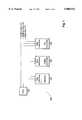
- FIG. 1is a signal flow diagram illustrating a computer system having memory and a CPU which communicate via a control bus, an address bus, and a data bus;
- FIG. 2is a block diagram of a first semiconductor memory architecture capable of storing multiple level logic states according to the present invention
- FIG. 3is a block diagram illustrating the function of a memory cell and a first embodiment of the read/write circuitry
- FIG. 4is a block diagram of an analog to digital converter capable of sensing more than two stored signal states and converting them to digital form;
- FIG. 5is a block diagram of a second semiconductor memory architecture capable of storing multiple level logic states according to the present invention.
- FIG. 6is a block diagram illustrating the function of a memory cell and a second embodiment of the read/write circuitry.
- FIG. 1a computer system 100 is shown having a CPU 102 coupled to three peripherals: a memory 104, a video controller 106, and an I/O controller 108.
- One or more bus bridge unitsmay be interposed between CPU 102 and the peripherals.
- Memory 104, video controller 106, and I/O controller 108each include a bus interface.
- memory 104includes memory cells capable of storing more than two logic states and read/write circuitry for storage and retrieval of these multiple logic states.
- the architecture of computer system 100allows CPU 102 to read from and write to peripherals via data bus 114.
- Address bus 112is used to indicate which device and data address CPU 102 wishes to access, and control bus 110 provides additional signaling lines which are used to indicate the type of access desired and to provide timing information.
- FIG. 2shows an exemplary memory architecture employed within computer system 100.
- memory 200has a ground plane 202 surrounding the chip circuitry which shields the circuitry from electromagnetic noise.
- Memory 200receives a chip enable signal, a read/write signal, and r address bit signals at an address decoder and refresh unit 206.
- address decoder and refresh unit 206asserts one of 2 r read word lines.
- Each of the read word linesis coupled to a row of memory cells.
- Each row of memory cellsis also coupled by a write word line to address controller 206.
- When a read word line is assertedthe corresponding row of memory cells may be read.
- a write word lineis asserted, the corresponding row of memory cells may be written.
- Memory 200also has n bi-directional binary data lines (D 0 -D n-1 ) connected to a bi-directional gate 204.
- Bi-directional gate 204is coupled to receive the read/write signal and is further coupled to m data paths which carry multi-value logic signals (S 0 -S m-1 ).
- Each of the data pathscan be driven by either bi-directional gate 204 or one of a set of analog-to-digital (A/D) converters 216-1 through 216-m (referred to collectively as A/D converters 216).
- A/D converters 216analog-to-digital converters 216-1 through 216-m
- Each of the data pathsprovides input to one of a set of data line drivers 212-1 through 212-m (referred to collectively as data line drivers 212).
- Data line drivers 212each serve to convert the multi-value logic signal into a multi-level voltage signal which is coupled by a data write line to a corresponding column of memory cells. Each column of memory cells is also coupled by a data read line to one of a set of sense amplifiers 214-1 through 214-m, which in turn provides input to one of the A/D converters 216.
- A/D converters 216convert the amplified signals to m multi-value logic signals (S 0 -S m-1 ) which are coupled to bi-directional gate 204.
- Bi-directional gate 204converts the m multi-value logic signal (S 0 -S m-1 ) to n binary digital signals, and drives the n bits on data lines D 0 -D n-1 . In this manner, a multi-value logic state stored in each cell may be read.
- the cells being readare refreshed concurrent with the read operation.
- data drivers 212convert the m multi-value logic signals (S 0 -S m-1 ) into m multi-level voltage signals and drive them on the data write lines which are coupled to cells 210. If at this time the word write line for word 0 is asserted, cells 210 store the m multi-level voltage signals. In this way, the content of cells 210 can be refreshed every time they are read.
- Bi-directional gate 204receives data from the bi-directional binary data lines D 0 -D n-1 and converts the data into m multi-value logic signals which are driven onto the m data paths.
- the A/D converters 216 for driving each of the m data pathsare disabled while the write/read control line indicates a write operation.
- Data line drivers 212convert the input m multi-value logic signals into m multi-level voltage signals and drives the data write lines coupled to the selected cells 210. Having the word write line asserted causes the multi-level signal to be stored in cells 210.
- Address decoder and refresh unit 206further includes refresh circuitry to read and refresh the contents of each memory cell within a given time interval.
- the refresh cyclescan be implemented in many ways, one of which is to have them happening continuously while the chip is not enabled.
- bi-directional gate 204is disabled and the A/D converters 216 are enabled during refresh cycles.
- Address decoder and refresh unit 206may employ a counter which sequentially asserts each word line, causing a read operation similar to that described previously. In order to assure that each memory cell is refreshed, the chip must spend a specified fraction of a given time interval in the disabled mode.
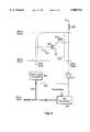
- FIG. 3illustrates a memory cell 210 which is exemplary of each of the cells of FIG. 2.
- Memory cell 210includes a storage transistor 302, a write transistor 304, and a read transistor 306.
- the gate of storage transistor 302is coupled via write transistor 304 to the data write line.
- Write transistor 304provides an electrically conductive path when the word write line is asserted, and an open circuit when the word line is de-asserted.
- an electric chargecan be stored on the gate by turning write transistor 304 on, passing a current through write transistor 304 to the gate of storage capacitor 302, and subsequently turning write transistor 304 off.
- the charge stored on the gatealters the conductivity of the channel of storage transistor 302.
- One terminal of storage transistor 302is connected to ground, and the other terminal is connected to read transistor 306.
- Read transistor 306provides an electrically conductive path when the word read line is asserted. The conductivity of storage transistor 302 can then be detected using the data read line.
- a pull-up resistance 309which may be implemented with a pull-up transistor, effects a voltage on the data read line which is indicative of the charge stored on the gate of storage transistor 302.
- Sense amplifier 214buffers and amplifies this voltage for A/D converter 214.
- A/D converter 216is enabled when the write/read signal indicates a read operation, and disabled when a write operation is indicated. When enabled, A/D converter 216 converts the amplified signal into a multi-value logic signal which is one of S 0 -S m-1 .
- Data line driver 212converts the multi-value logic signal into a multi-level voltage on the data write line.
- FIG. 4shows a block diagram of one embodiment of A/D converter 216.
- A/D converter 216receives an input signal 402 and drives a digital output signal on L-1 output lines 404-408 (which form a data path to carry one of the multi-value logic signals S 0 -S m-1 ) when enabled by a write/read signal 410.
- asserting write/read signal 410drives the output lines to a high impedance state.
- A/D converter 400is comprised of L- 1 comparators 412, where L is the number of logic states which can be stored in a memory cell 308. Each comparator receives one of L-1 reference voltages which demarcate the voltage regions representative of each logic state.
- comparator 412-1compares input signal 402 to reference voltage V 1 , and (if enabled) asserts output line 404 when input signal 402 exceeds the reference voltage.
- the L- 1 output linesaccordingly have L possible states, ranging from having no lines asserted to having L-1 lines asserted.
- bi-directional gate 204converts the input received at eight binary data lines D 0 -D 7 to four quaternary logic signals S 0 -S 3 .
- Each of the logic signalsis converted to a corresponding voltage on a data write line by a data line driver 212.
- the voltage at each data write lineresults in one of four charge quantities to be stored on the gate of the corresponding storage transistor 302 being written.
- the charge stored on each storage transistor 302results in one of four possible channel conductivities which induces one of four possible voltages at the outputs of the sense amplifiers 214.
- the possible output voltagesmay be 0, V/3, 2V/3, and V, where V is the supply voltage.
- A/D converters 216each include three output lines and three reference voltages which may be V/6, V/2, and 5V/6. Thus, if the output voltage of a particular cell 210 sensed by a sense amplifier 214 is 2V/3, two of the three output lines are asserted by A/D converter 216 (when enabled).
- FIG. 5shows a second exemplary memory architecture employed within computer system 100. Circuit portions that correspond to those of FIG. 2 are numbered identically.
- Memory 500is similar to memory 200; however, in memory 500 a set of delay elements 508 is coupled between the read word lines and the write word lines.
- a set of data level controllers 512which implement the functionality of data drivers 212, is used to write to memory cells. Additional functionality of data level controllers 512 is described further below.
- a feedback path between sense amplifiers 214 and data level controllers 512is also shown in FIG. 5, and is discussed further below.
- Delay elements 508are configured to momentarily assert a write word line upon a preset delay following the assertion of a corresponding read word line. In this implementation, the read word line remains asserted until after the write word line assertion is terminated. Configuring delay elements 508 in this manner causes every memory access to comprise a read followed by a write. When the desired memory access is a read operation, the following write operation merely refreshes the cell contents. When the desired memory access is a write operation, the cell contents are replaced with new values. In both cases, the write operation is accomplished in accordance with respective outputs from data level controllers 512 while the cells' contents are detected by sense amplifiers 214.
- Data level controller 512is configured to accept a multi-value logic signal input 602 as a set point (i.e. an indicator of a desired voltage level at node 604). Data level controller 512 then provides a voltage signal on the data write line, and adjusts it until the output signal from sense amplifier 214 is equal to the desired voltage level which corresponds to the multi-value logic input signal 602. For example, if the defined values of the multi-value logic signal are 0, 1, 2, and 3 (in a four-level logic system), the voltage levels which might be chosen to correspond to these values are 0, V/3, 2V/3, and V, where V is the supply voltage.
- data level controller 512Upon receiving an input signal value of 1 at input 602, data level controller 512 initially drives the data write line an initial voltage so as to provide for a voltage drop across storage transistor 302 of V/3. If the sense amplifier output signal is higher than V/3 (due for example to memory cell variations or the resistance of read transistor 306 ), data level controller 512 adjusts the voltage on the data write line to reduce the voltage drop across storage transistor 302 until the sense amplifier output signal equals V/3. Data level controller 512 may also adjust the data write line voltage in the opposite direction when the sense amplifier output signal is lower than V/3.
- Memory circuit 500advantageously accommodates the storage of more than two logic states in a memory cell.
- the feedback implementationadjusts the stored charge of memory cell 210 in order to ensure an accurate retrieval of the logic state. Accurate retrieval of logic states is essential to the reliability of any multi-level logic storage method using DRAMs, since the increased number of logic states reduces the margin for error.
Landscapes
- Engineering & Computer Science (AREA)
- Computer Hardware Design (AREA)
- Dram (AREA)
- Read Only Memory (AREA)
- Static Random-Access Memory (AREA)
Abstract
Description
Claims (18)
Priority Applications (2)
| Application Number | Priority Date | Filing Date | Title |
|---|---|---|---|
| US08/779,991US5808932A (en) | 1996-12-23 | 1996-12-23 | Memory system which enables storage and retrieval of more than two states in a memory cell |
| JP9370127AJPH10228781A (en) | 1996-12-23 | 1997-12-24 | Memory system which can store and retrieve states of three or more in memory cell |
Applications Claiming Priority (1)
| Application Number | Priority Date | Filing Date | Title |
|---|---|---|---|
| US08/779,991US5808932A (en) | 1996-12-23 | 1996-12-23 | Memory system which enables storage and retrieval of more than two states in a memory cell |
Publications (1)
| Publication Number | Publication Date |
|---|---|
| US5808932Atrue US5808932A (en) | 1998-09-15 |
Family
ID=25118231
Family Applications (1)
| Application Number | Title | Priority Date | Filing Date |
|---|---|---|---|
| US08/779,991Expired - LifetimeUS5808932A (en) | 1996-12-23 | 1996-12-23 | Memory system which enables storage and retrieval of more than two states in a memory cell |
Country Status (2)
| Country | Link |
|---|---|
| US (1) | US5808932A (en) |
| JP (1) | JPH10228781A (en) |
Cited By (26)
| Publication number | Priority date | Publication date | Assignee | Title |
|---|---|---|---|---|
| US6021064A (en)* | 1998-02-04 | 2000-02-01 | Vlsi Technology, Inc. | Layout for data storage circuit using shared bit line and method therefor |
| US6046931A (en)* | 1997-12-11 | 2000-04-04 | Evsx, Inc. | Method and apparatus for a RAM circuit having N-nary output interface |
| US6066965A (en)* | 1997-12-11 | 2000-05-23 | Evsx, Inc. | Method and apparatus for a N-nary logic circuit using 1 of 4 signals |
| US6069497A (en)* | 1997-12-11 | 2000-05-30 | Evsx, Inc. | Method and apparatus for a N-nary logic circuit using 1 of N signals |
| US6072713A (en)* | 1998-02-04 | 2000-06-06 | Vlsi Technology, Inc. | Data storage circuit using shared bit line and method therefor |
| US6084797A (en)* | 1998-03-27 | 2000-07-04 | Stmicroelectronics S.R.L. | Method for reading a multiple-level memory cell |
| US6154065A (en)* | 1997-11-28 | 2000-11-28 | Sharp Kabushiki Kaisha | Sense amplifier circuit |
| US6266269B1 (en)* | 2000-06-07 | 2001-07-24 | Xilinx, Inc. | Three terminal non-volatile memory element |
| US6430098B1 (en)* | 2000-05-16 | 2002-08-06 | Broadcom Corporation | Transparent continuous refresh RAM cell architecture |
| US6496950B1 (en) | 1999-08-11 | 2002-12-17 | Lsi Logic Corporation | Testing content addressable static memories |
| US6550032B1 (en) | 1999-07-28 | 2003-04-15 | Lsi Logic Corporation | Detecting interport faults in multiport static memories |
| US20040085813A1 (en)* | 2002-11-04 | 2004-05-06 | Dialog Semiconductor Gmbh | Multiple level RAM device |
| US6757854B1 (en) | 1999-09-16 | 2004-06-29 | Lsi Logic Corporation | Detecting faults in dual port FIFO memories |
| US20080205120A1 (en)* | 2007-02-23 | 2008-08-28 | Chih-Ta Star Sung | Multiple layer random accessing memory |
| US7420842B1 (en) | 2005-08-24 | 2008-09-02 | Xilinx, Inc. | Method of programming a three-terminal non-volatile memory element using source-drain bias |
| US7450431B1 (en) | 2005-08-24 | 2008-11-11 | Xilinx, Inc. | PMOS three-terminal non-volatile memory element and method of programming |
| US20090097308A1 (en)* | 2007-10-15 | 2009-04-16 | Rao G R Mohan | Multivalue memory storage with two gating transistors |
| US7544968B1 (en) | 2005-08-24 | 2009-06-09 | Xilinx, Inc. | Non-volatile memory cell with charge storage element and method of programming |
| US7687797B1 (en) | 2005-08-24 | 2010-03-30 | Xilinx, Inc. | Three-terminal non-volatile memory element with hybrid gate dielectric |
| US7745301B2 (en) | 2005-08-22 | 2010-06-29 | Terapede, Llc | Methods and apparatus for high-density chip connectivity |
| US20120224404A1 (en)* | 2011-01-27 | 2012-09-06 | Anobit Technologies Ltd. | Enhanced programming and erasure schemes for analog memory cells |
| US8957511B2 (en) | 2005-08-22 | 2015-02-17 | Madhukar B. Vora | Apparatus and methods for high-density chip connectivity |
| US9401200B1 (en) | 2014-12-22 | 2016-07-26 | Altera Corporation | Memory cells with p-type diffusion read-only port |
| US9660024B2 (en) | 2014-12-18 | 2017-05-23 | Samsung Electronics Co., Ltd. | Semiconductor device with two transistors and a capacitor |
| US10402366B2 (en)* | 2006-08-21 | 2019-09-03 | Benjamin J. Cooper | Efficient and scalable multi-value processor and supporting circuits |
| US10985162B2 (en)* | 2018-12-14 | 2021-04-20 | John Bennett | System for accurate multiple level gain cells |
Families Citing this family (3)
| Publication number | Priority date | Publication date | Assignee | Title |
|---|---|---|---|---|
| JP2002133876A (en) | 2000-10-23 | 2002-05-10 | Hitachi Ltd | Semiconductor storage device |
| KR101893332B1 (en)* | 2009-11-13 | 2018-08-31 | 가부시키가이샤 한도오따이 에네루기 켄큐쇼 | Semiconductor device and driving method thereof |
| TWI595502B (en)* | 2012-05-18 | 2017-08-11 | 半導體能源研究所股份有限公司 | Memory device and method for driving a memory device |
Citations (20)
| Publication number | Priority date | Publication date | Assignee | Title |
|---|---|---|---|---|
| US4057788A (en)* | 1974-10-21 | 1977-11-08 | Raytheon Company | Semiconductor memory structures |
| US4633438A (en)* | 1983-12-19 | 1986-12-30 | Hitachi, Ltd. | Stacked semiconductor memory |
| US4661929A (en)* | 1983-12-23 | 1987-04-28 | Hitachi, Ltd. | Semiconductor memory having multiple level storage structure |
| US4715014A (en)* | 1985-10-29 | 1987-12-22 | Texas Instruments Incorporated | Modified three transistor EEPROM cell |
| US4910709A (en)* | 1988-08-10 | 1990-03-20 | International Business Machines Corporation | Complementary metal-oxide-semiconductor transistor and one-capacitor dynamic-random-access memory cell |
| US4935896A (en)* | 1987-11-24 | 1990-06-19 | Mitsubishi Denki Kabushiki Kaisha | Semiconductor memory device having three-transistor type memory cells structure without additional gates |
| US5021999A (en)* | 1987-12-17 | 1991-06-04 | Mitsubishi Denki Kabushiki Kaisha | Non-volatile semiconductor memory device with facility of storing tri-level data |
| US5119330A (en)* | 1989-03-31 | 1992-06-02 | Oki Electric Industry Co, Ltd. | Nonvolatile memory system for multiple value storing |
| US5159570A (en)* | 1987-12-22 | 1992-10-27 | Texas Instruments Incorporated | Four memory state EEPROM |
| US5172338A (en)* | 1989-04-13 | 1992-12-15 | Sundisk Corporation | Multi-state EEprom read and write circuits and techniques |
| US5262988A (en)* | 1991-05-17 | 1993-11-16 | Kabushiki Kaisha Toshiba | Dynamic memory cell and dynamic memory |
| US5282162A (en)* | 1990-05-24 | 1994-01-25 | Kabushiki Kaisha Toshiba | Semiconductor memory device having capacitor of thin film transistor structure |
| US5283761A (en)* | 1992-07-22 | 1994-02-01 | Mosaid Technologies Incorporated | Method of multi-level storage in DRAM |
| US5351210A (en)* | 1990-11-28 | 1994-09-27 | Kabushiki Kaisha Toshiba | Serially accessible semiconductor memory with multiple level storage cells |
| US5357464A (en)* | 1992-03-02 | 1994-10-18 | Hitachi, Ltd. | Semiconductor memory having writing and reading transistors, method of fabrication thereof, and method of use thereof |
| US5394362A (en)* | 1991-02-08 | 1995-02-28 | Banks; Gerald J. | Electrically alterable non-voltatile memory with N-bits per memory cell |
| US5459686A (en)* | 1993-10-15 | 1995-10-17 | Solidas Corporation | Multiple level random access memory |
| US5521865A (en)* | 1994-03-15 | 1996-05-28 | Kabushiki Kaisha Toshiba | Non-volatile semiconductor memory device for storing multi-value data |
| US5532955A (en)* | 1994-12-30 | 1996-07-02 | Mosaid Technologies Incorporated | Method of multilevel dram sense and restore |
| US5646903A (en)* | 1996-03-06 | 1997-07-08 | Xilinx, Inc. | Memory cell having a shared read/write line |
- 1996
- 1996-12-23USUS08/779,991patent/US5808932A/ennot_activeExpired - Lifetime
- 1997
- 1997-12-24JPJP9370127Apatent/JPH10228781A/enactivePending
Patent Citations (21)
| Publication number | Priority date | Publication date | Assignee | Title |
|---|---|---|---|---|
| US4057788A (en)* | 1974-10-21 | 1977-11-08 | Raytheon Company | Semiconductor memory structures |
| US4633438A (en)* | 1983-12-19 | 1986-12-30 | Hitachi, Ltd. | Stacked semiconductor memory |
| US4661929A (en)* | 1983-12-23 | 1987-04-28 | Hitachi, Ltd. | Semiconductor memory having multiple level storage structure |
| US4715014A (en)* | 1985-10-29 | 1987-12-22 | Texas Instruments Incorporated | Modified three transistor EEPROM cell |
| US4935896A (en)* | 1987-11-24 | 1990-06-19 | Mitsubishi Denki Kabushiki Kaisha | Semiconductor memory device having three-transistor type memory cells structure without additional gates |
| US5021999A (en)* | 1987-12-17 | 1991-06-04 | Mitsubishi Denki Kabushiki Kaisha | Non-volatile semiconductor memory device with facility of storing tri-level data |
| US5159570A (en)* | 1987-12-22 | 1992-10-27 | Texas Instruments Incorporated | Four memory state EEPROM |
| US4910709A (en)* | 1988-08-10 | 1990-03-20 | International Business Machines Corporation | Complementary metal-oxide-semiconductor transistor and one-capacitor dynamic-random-access memory cell |
| US5119330A (en)* | 1989-03-31 | 1992-06-02 | Oki Electric Industry Co, Ltd. | Nonvolatile memory system for multiple value storing |
| US5172338A (en)* | 1989-04-13 | 1992-12-15 | Sundisk Corporation | Multi-state EEprom read and write circuits and techniques |
| US5172338B1 (en)* | 1989-04-13 | 1997-07-08 | Sandisk Corp | Multi-state eeprom read and write circuits and techniques |
| US5282162A (en)* | 1990-05-24 | 1994-01-25 | Kabushiki Kaisha Toshiba | Semiconductor memory device having capacitor of thin film transistor structure |
| US5351210A (en)* | 1990-11-28 | 1994-09-27 | Kabushiki Kaisha Toshiba | Serially accessible semiconductor memory with multiple level storage cells |
| US5394362A (en)* | 1991-02-08 | 1995-02-28 | Banks; Gerald J. | Electrically alterable non-voltatile memory with N-bits per memory cell |
| US5262988A (en)* | 1991-05-17 | 1993-11-16 | Kabushiki Kaisha Toshiba | Dynamic memory cell and dynamic memory |
| US5357464A (en)* | 1992-03-02 | 1994-10-18 | Hitachi, Ltd. | Semiconductor memory having writing and reading transistors, method of fabrication thereof, and method of use thereof |
| US5283761A (en)* | 1992-07-22 | 1994-02-01 | Mosaid Technologies Incorporated | Method of multi-level storage in DRAM |
| US5459686A (en)* | 1993-10-15 | 1995-10-17 | Solidas Corporation | Multiple level random access memory |
| US5521865A (en)* | 1994-03-15 | 1996-05-28 | Kabushiki Kaisha Toshiba | Non-volatile semiconductor memory device for storing multi-value data |
| US5532955A (en)* | 1994-12-30 | 1996-07-02 | Mosaid Technologies Incorporated | Method of multilevel dram sense and restore |
| US5646903A (en)* | 1996-03-06 | 1997-07-08 | Xilinx, Inc. | Memory cell having a shared read/write line |
Non-Patent Citations (2)
| Title |
|---|
| Abbott, et al., "A 4K MOS Dynamic Random-Access Memory," IEEE Journal of Solid-State Circuits, vol. SC-8, No. 5, Oct. 1973, pp. 292-298. |
| Abbott, et al., A 4K MOS Dynamic Random Access Memory, IEEE Journal of Solid State Circuits, vol. SC 8, No. 5, Oct. 1973, pp. 292 298.* |
Cited By (39)
| Publication number | Priority date | Publication date | Assignee | Title |
|---|---|---|---|---|
| US6154065A (en)* | 1997-11-28 | 2000-11-28 | Sharp Kabushiki Kaisha | Sense amplifier circuit |
| US6046931A (en)* | 1997-12-11 | 2000-04-04 | Evsx, Inc. | Method and apparatus for a RAM circuit having N-nary output interface |
| US6066965A (en)* | 1997-12-11 | 2000-05-23 | Evsx, Inc. | Method and apparatus for a N-nary logic circuit using 1 of 4 signals |
| US6069497A (en)* | 1997-12-11 | 2000-05-30 | Evsx, Inc. | Method and apparatus for a N-nary logic circuit using 1 of N signals |
| US6252425B1 (en) | 1997-12-11 | 2001-06-26 | Intrinsity, Inc. | Method and apparatus for an N-NARY logic circuit |
| US6181596B1 (en)* | 1997-12-11 | 2001-01-30 | Intrinsity, Inc. | Method and apparatus for a RAM circuit having N-Nary output interface |
| US6072713A (en)* | 1998-02-04 | 2000-06-06 | Vlsi Technology, Inc. | Data storage circuit using shared bit line and method therefor |
| US6021064A (en)* | 1998-02-04 | 2000-02-01 | Vlsi Technology, Inc. | Layout for data storage circuit using shared bit line and method therefor |
| US6084797A (en)* | 1998-03-27 | 2000-07-04 | Stmicroelectronics S.R.L. | Method for reading a multiple-level memory cell |
| US6550032B1 (en) | 1999-07-28 | 2003-04-15 | Lsi Logic Corporation | Detecting interport faults in multiport static memories |
| US6496950B1 (en) | 1999-08-11 | 2002-12-17 | Lsi Logic Corporation | Testing content addressable static memories |
| US6757854B1 (en) | 1999-09-16 | 2004-06-29 | Lsi Logic Corporation | Detecting faults in dual port FIFO memories |
| US6430098B1 (en)* | 2000-05-16 | 2002-08-06 | Broadcom Corporation | Transparent continuous refresh RAM cell architecture |
| US6600677B2 (en) | 2000-05-16 | 2003-07-29 | Broadcom Corporation | Memory circuit capable of simultaneous writing and refreshing on the same column and a memory cell for application in the same |
| US6717863B2 (en) | 2000-05-16 | 2004-04-06 | Broadcom Corporation | Transparent continuous refresh RAM cell architecture |
| US6888761B2 (en) | 2000-05-16 | 2005-05-03 | Broadcom Corporation | Memory device having simultaneous read/write and refresh operations with coincident phases |
| US20040184335A1 (en)* | 2000-05-16 | 2004-09-23 | Broadcom Corporation | Transparent continuous refresh RAM cell architecture |
| US6266269B1 (en)* | 2000-06-07 | 2001-07-24 | Xilinx, Inc. | Three terminal non-volatile memory element |
| EP1416496A1 (en)* | 2002-11-04 | 2004-05-06 | Dialog Semiconductor GmbH | Multiple level ram device |
| US6801445B2 (en) | 2002-11-04 | 2004-10-05 | Dialog Semiconductor Gmbh | Multiple level RAM device |
| US20040085813A1 (en)* | 2002-11-04 | 2004-05-06 | Dialog Semiconductor Gmbh | Multiple level RAM device |
| US8957511B2 (en) | 2005-08-22 | 2015-02-17 | Madhukar B. Vora | Apparatus and methods for high-density chip connectivity |
| US7745301B2 (en) | 2005-08-22 | 2010-06-29 | Terapede, Llc | Methods and apparatus for high-density chip connectivity |
| US7687797B1 (en) | 2005-08-24 | 2010-03-30 | Xilinx, Inc. | Three-terminal non-volatile memory element with hybrid gate dielectric |
| US7947980B1 (en) | 2005-08-24 | 2011-05-24 | Xilinx, Inc. | Non-volatile memory cell with charge storage element and method of programming |
| US7544968B1 (en) | 2005-08-24 | 2009-06-09 | Xilinx, Inc. | Non-volatile memory cell with charge storage element and method of programming |
| US7450431B1 (en) | 2005-08-24 | 2008-11-11 | Xilinx, Inc. | PMOS three-terminal non-volatile memory element and method of programming |
| US7420842B1 (en) | 2005-08-24 | 2008-09-02 | Xilinx, Inc. | Method of programming a three-terminal non-volatile memory element using source-drain bias |
| US10402366B2 (en)* | 2006-08-21 | 2019-09-03 | Benjamin J. Cooper | Efficient and scalable multi-value processor and supporting circuits |
| US20080205120A1 (en)* | 2007-02-23 | 2008-08-28 | Chih-Ta Star Sung | Multiple layer random accessing memory |
| US7609546B2 (en) | 2007-10-15 | 2009-10-27 | Rao G R Mohan | Multivalue memory storage with two gating transistors |
| CN101828233B (en)* | 2007-10-15 | 2015-01-14 | S.阿夸半导体有限公司 | Multi-value storage device, system and method |
| US20090097308A1 (en)* | 2007-10-15 | 2009-04-16 | Rao G R Mohan | Multivalue memory storage with two gating transistors |
| WO2009052013A1 (en) | 2007-10-15 | 2009-04-23 | S. Aqua Semiconductor Llc | Multivalue memory storage with two gating transistors |
| US20120224404A1 (en)* | 2011-01-27 | 2012-09-06 | Anobit Technologies Ltd. | Enhanced programming and erasure schemes for analog memory cells |
| US8649200B2 (en)* | 2011-01-27 | 2014-02-11 | Apple Inc. | Enhanced programming and erasure schemes for analog memory cells |
| US9660024B2 (en) | 2014-12-18 | 2017-05-23 | Samsung Electronics Co., Ltd. | Semiconductor device with two transistors and a capacitor |
| US9401200B1 (en) | 2014-12-22 | 2016-07-26 | Altera Corporation | Memory cells with p-type diffusion read-only port |
| US10985162B2 (en)* | 2018-12-14 | 2021-04-20 | John Bennett | System for accurate multiple level gain cells |
Also Published As
| Publication number | Publication date |
|---|---|
| JPH10228781A (en) | 1998-08-25 |
Similar Documents
| Publication | Publication Date | Title |
|---|---|---|
| US5808932A (en) | Memory system which enables storage and retrieval of more than two states in a memory cell | |
| US5784328A (en) | Memory system including an on-chip temperature sensor for regulating the refresh rate of a DRAM array | |
| US5982659A (en) | Memory cell capable of storing more than two logic states by using different via resistances | |
| US5761110A (en) | Memory cell capable of storing more than two logic states by using programmable resistances | |
| US5841695A (en) | Memory system using multiple storage mechanisms to enable storage and retrieval of more than two states in a memory cell | |
| US5539690A (en) | Write verify schemes for flash memory with multilevel cells | |
| US5351210A (en) | Serially accessible semiconductor memory with multiple level storage cells | |
| US5867423A (en) | Memory circuit and method for multivalued logic storage by process variations | |
| US5485422A (en) | Drain bias multiplexing for multiple bit flash cell | |
| US6813208B2 (en) | System and method for sensing data stored in a resistive memory element using one bit of a digital count | |
| US4905197A (en) | Semiconductor memory having circuitry for discharging a digit line before verifying operation | |
| EP1754231A2 (en) | Memory device with user configurable density/performance | |
| US5847990A (en) | Ram cell capable of storing 3 logic states | |
| EP0486794A2 (en) | DRAM having extended refresh time | |
| US7440352B2 (en) | Semiconductor memory device capable of selectively refreshing word lines | |
| US7483324B2 (en) | Memory device and method providing an average threshold based refresh mechanism | |
| US10990317B2 (en) | Memory with automatic background precondition upon powerup | |
| US6731556B2 (en) | DRAM with bias sensing | |
| US20240153558A1 (en) | Resistive memory with enhanced redundancy writing | |
| US11699479B2 (en) | Nonvolatile memory apparatus for generating read reference and an operating method of the nonvolatile memory apparatus | |
| US11532358B2 (en) | Memory with automatic background precondition upon powerup | |
| KR20250075423A (en) | Non-volatile memory device and operation method thereof to provide memory read and write based on exclusive or | |
| CN118366506A (en) | Random access memory and electronic equipment | |
| KR19990003406A (en) | Memory device having multi-level cells and data writing method thereof |
Legal Events
| Date | Code | Title | Description |
|---|---|---|---|
| AS | Assignment | Owner name:NIPPON FURNACE KOGYO KABUSHIKI KAISHA, JAPAN Free format text:ASSIGNMENT OF ASSIGNORS INTEREST;ASSIGNOR:KATSUKI, MASASHI;REEL/FRAME:009004/0104 Effective date:19970120 | |
| AS | Assignment | Owner name:LSI LOGIC CORPORATION, CALIFORNIA Free format text:ASSIGNMENT OF ASSIGNORS INTEREST;ASSIGNORS:KAPOOR, ASHOK;OWENS, ALEX;WIK, THOMAS R.;AND OTHERS;REEL/FRAME:008571/0271 Effective date:19970421 | |
| STCF | Information on status: patent grant | Free format text:PATENTED CASE | |
| FPAY | Fee payment | Year of fee payment:4 | |
| FPAY | Fee payment | Year of fee payment:8 | |
| FEPP | Fee payment procedure | Free format text:PAYOR NUMBER ASSIGNED (ORIGINAL EVENT CODE: ASPN); ENTITY STATUS OF PATENT OWNER: LARGE ENTITY Free format text:PAYER NUMBER DE-ASSIGNED (ORIGINAL EVENT CODE: RMPN); ENTITY STATUS OF PATENT OWNER: LARGE ENTITY | |
| FPAY | Fee payment | Year of fee payment:12 | |
| AS | Assignment | Owner name:DEUTSCHE BANK AG NEW YORK BRANCH, AS COLLATERAL AG Free format text:PATENT SECURITY AGREEMENT;ASSIGNORS:LSI CORPORATION;AGERE SYSTEMS LLC;REEL/FRAME:032856/0031 Effective date:20140506 | |
| AS | Assignment | Owner name:LSI CORPORATION, CALIFORNIA Free format text:CHANGE OF NAME;ASSIGNOR:LSI LOGIC CORPORATION;REEL/FRAME:033102/0270 Effective date:20070406 | |
| AS | Assignment | Owner name:AVAGO TECHNOLOGIES GENERAL IP (SINGAPORE) PTE. LTD Free format text:ASSIGNMENT OF ASSIGNORS INTEREST;ASSIGNOR:LSI CORPORATION;REEL/FRAME:035390/0388 Effective date:20140814 | |
| AS | Assignment | Owner name:AGERE SYSTEMS LLC, PENNSYLVANIA Free format text:TERMINATION AND RELEASE OF SECURITY INTEREST IN PATENT RIGHTS (RELEASES RF 032856-0031);ASSIGNOR:DEUTSCHE BANK AG NEW YORK BRANCH, AS COLLATERAL AGENT;REEL/FRAME:037684/0039 Effective date:20160201 Owner name:LSI CORPORATION, CALIFORNIA Free format text:TERMINATION AND RELEASE OF SECURITY INTEREST IN PATENT RIGHTS (RELEASES RF 032856-0031);ASSIGNOR:DEUTSCHE BANK AG NEW YORK BRANCH, AS COLLATERAL AGENT;REEL/FRAME:037684/0039 Effective date:20160201 | |
| AS | Assignment | Owner name:BANK OF AMERICA, N.A., AS COLLATERAL AGENT, NORTH CAROLINA Free format text:PATENT SECURITY AGREEMENT;ASSIGNOR:AVAGO TECHNOLOGIES GENERAL IP (SINGAPORE) PTE. LTD.;REEL/FRAME:037808/0001 Effective date:20160201 Owner name:BANK OF AMERICA, N.A., AS COLLATERAL AGENT, NORTH Free format text:PATENT SECURITY AGREEMENT;ASSIGNOR:AVAGO TECHNOLOGIES GENERAL IP (SINGAPORE) PTE. LTD.;REEL/FRAME:037808/0001 Effective date:20160201 | |
| AS | Assignment | Owner name:AVAGO TECHNOLOGIES GENERAL IP (SINGAPORE) PTE. LTD., SINGAPORE Free format text:TERMINATION AND RELEASE OF SECURITY INTEREST IN PATENTS;ASSIGNOR:BANK OF AMERICA, N.A., AS COLLATERAL AGENT;REEL/FRAME:041710/0001 Effective date:20170119 Owner name:AVAGO TECHNOLOGIES GENERAL IP (SINGAPORE) PTE. LTD Free format text:TERMINATION AND RELEASE OF SECURITY INTEREST IN PATENTS;ASSIGNOR:BANK OF AMERICA, N.A., AS COLLATERAL AGENT;REEL/FRAME:041710/0001 Effective date:20170119 |