US5808873A - Electronic component assembly having an encapsulation material and method of forming the same - Google Patents
Electronic component assembly having an encapsulation material and method of forming the sameDownload PDFInfo
- Publication number
- US5808873A US5808873AUS08/865,652US86565297AUS5808873AUS 5808873 AUS5808873 AUS 5808873AUS 86565297 AUS86565297 AUS 86565297AUS 5808873 AUS5808873 AUS 5808873A
- Authority
- US
- United States
- Prior art keywords
- electronic component
- trench
- edge
- masking layer
- component assembly
- Prior art date
- Legal status (The legal status is an assumption and is not a legal conclusion. Google has not performed a legal analysis and makes no representation as to the accuracy of the status listed.)
- Expired - Lifetime
Links
Images
Classifications
- H—ELECTRICITY
- H01—ELECTRIC ELEMENTS
- H01L—SEMICONDUCTOR DEVICES NOT COVERED BY CLASS H10
- H01L23/00—Details of semiconductor or other solid state devices
- H01L23/28—Encapsulations, e.g. encapsulating layers, coatings, e.g. for protection
- H—ELECTRICITY
- H01—ELECTRIC ELEMENTS
- H01L—SEMICONDUCTOR DEVICES NOT COVERED BY CLASS H10
- H01L24/00—Arrangements for connecting or disconnecting semiconductor or solid-state bodies; Methods or apparatus related thereto
- H01L24/01—Means for bonding being attached to, or being formed on, the surface to be connected, e.g. chip-to-package, die-attach, "first-level" interconnects; Manufacturing methods related thereto
- H01L24/42—Wire connectors; Manufacturing methods related thereto
- H01L24/47—Structure, shape, material or disposition of the wire connectors after the connecting process
- H01L24/48—Structure, shape, material or disposition of the wire connectors after the connecting process of an individual wire connector
- H—ELECTRICITY
- H01—ELECTRIC ELEMENTS
- H01L—SEMICONDUCTOR DEVICES NOT COVERED BY CLASS H10
- H01L23/00—Details of semiconductor or other solid state devices
- H01L23/28—Encapsulations, e.g. encapsulating layers, coatings, e.g. for protection
- H01L23/31—Encapsulations, e.g. encapsulating layers, coatings, e.g. for protection characterised by the arrangement or shape
- H01L23/3107—Encapsulations, e.g. encapsulating layers, coatings, e.g. for protection characterised by the arrangement or shape the device being completely enclosed
- H01L23/3121—Encapsulations, e.g. encapsulating layers, coatings, e.g. for protection characterised by the arrangement or shape the device being completely enclosed a substrate forming part of the encapsulation
- H—ELECTRICITY
- H01—ELECTRIC ELEMENTS
- H01L—SEMICONDUCTOR DEVICES NOT COVERED BY CLASS H10
- H01L2224/00—Indexing scheme for arrangements for connecting or disconnecting semiconductor or solid-state bodies and methods related thereto as covered by H01L24/00
- H01L2224/01—Means for bonding being attached to, or being formed on, the surface to be connected, e.g. chip-to-package, die-attach, "first-level" interconnects; Manufacturing methods related thereto
- H01L2224/02—Bonding areas; Manufacturing methods related thereto
- H01L2224/04—Structure, shape, material or disposition of the bonding areas prior to the connecting process
- H01L2224/05—Structure, shape, material or disposition of the bonding areas prior to the connecting process of an individual bonding area
- H01L2224/0554—External layer
- H01L2224/05599—Material
- H—ELECTRICITY
- H01—ELECTRIC ELEMENTS
- H01L—SEMICONDUCTOR DEVICES NOT COVERED BY CLASS H10
- H01L2224/00—Indexing scheme for arrangements for connecting or disconnecting semiconductor or solid-state bodies and methods related thereto as covered by H01L24/00
- H01L2224/01—Means for bonding being attached to, or being formed on, the surface to be connected, e.g. chip-to-package, die-attach, "first-level" interconnects; Manufacturing methods related thereto
- H01L2224/42—Wire connectors; Manufacturing methods related thereto
- H01L2224/44—Structure, shape, material or disposition of the wire connectors prior to the connecting process
- H01L2224/45—Structure, shape, material or disposition of the wire connectors prior to the connecting process of an individual wire connector
- H01L2224/45001—Core members of the connector
- H01L2224/45099—Material
- H01L2224/451—Material with a principal constituent of the material being a metal or a metalloid, e.g. boron (B), silicon (Si), germanium (Ge), arsenic (As), antimony (Sb), tellurium (Te) and polonium (Po), and alloys thereof
- H—ELECTRICITY
- H01—ELECTRIC ELEMENTS
- H01L—SEMICONDUCTOR DEVICES NOT COVERED BY CLASS H10
- H01L2224/00—Indexing scheme for arrangements for connecting or disconnecting semiconductor or solid-state bodies and methods related thereto as covered by H01L24/00
- H01L2224/01—Means for bonding being attached to, or being formed on, the surface to be connected, e.g. chip-to-package, die-attach, "first-level" interconnects; Manufacturing methods related thereto
- H01L2224/42—Wire connectors; Manufacturing methods related thereto
- H01L2224/47—Structure, shape, material or disposition of the wire connectors after the connecting process
- H01L2224/48—Structure, shape, material or disposition of the wire connectors after the connecting process of an individual wire connector
- H01L2224/4805—Shape
- H01L2224/4809—Loop shape
- H01L2224/48091—Arched
- H—ELECTRICITY
- H01—ELECTRIC ELEMENTS
- H01L—SEMICONDUCTOR DEVICES NOT COVERED BY CLASS H10
- H01L2224/00—Indexing scheme for arrangements for connecting or disconnecting semiconductor or solid-state bodies and methods related thereto as covered by H01L24/00
- H01L2224/01—Means for bonding being attached to, or being formed on, the surface to be connected, e.g. chip-to-package, die-attach, "first-level" interconnects; Manufacturing methods related thereto
- H01L2224/42—Wire connectors; Manufacturing methods related thereto
- H01L2224/47—Structure, shape, material or disposition of the wire connectors after the connecting process
- H01L2224/48—Structure, shape, material or disposition of the wire connectors after the connecting process of an individual wire connector
- H01L2224/481—Disposition
- H01L2224/48151—Connecting between a semiconductor or solid-state body and an item not being a semiconductor or solid-state body, e.g. chip-to-substrate, chip-to-passive
- H01L2224/48221—Connecting between a semiconductor or solid-state body and an item not being a semiconductor or solid-state body, e.g. chip-to-substrate, chip-to-passive the body and the item being stacked
- H01L2224/48225—Connecting between a semiconductor or solid-state body and an item not being a semiconductor or solid-state body, e.g. chip-to-substrate, chip-to-passive the body and the item being stacked the item being non-metallic, e.g. insulating substrate with or without metallisation
- H01L2224/48227—Connecting between a semiconductor or solid-state body and an item not being a semiconductor or solid-state body, e.g. chip-to-substrate, chip-to-passive the body and the item being stacked the item being non-metallic, e.g. insulating substrate with or without metallisation connecting the wire to a bond pad of the item
- H01L2224/48228—Connecting between a semiconductor or solid-state body and an item not being a semiconductor or solid-state body, e.g. chip-to-substrate, chip-to-passive the body and the item being stacked the item being non-metallic, e.g. insulating substrate with or without metallisation connecting the wire to a bond pad of the item the bond pad being disposed in a recess of the surface of the item
- H—ELECTRICITY
- H01—ELECTRIC ELEMENTS
- H01L—SEMICONDUCTOR DEVICES NOT COVERED BY CLASS H10
- H01L2224/00—Indexing scheme for arrangements for connecting or disconnecting semiconductor or solid-state bodies and methods related thereto as covered by H01L24/00
- H01L2224/01—Means for bonding being attached to, or being formed on, the surface to be connected, e.g. chip-to-package, die-attach, "first-level" interconnects; Manufacturing methods related thereto
- H01L2224/42—Wire connectors; Manufacturing methods related thereto
- H01L2224/47—Structure, shape, material or disposition of the wire connectors after the connecting process
- H01L2224/48—Structure, shape, material or disposition of the wire connectors after the connecting process of an individual wire connector
- H01L2224/484—Connecting portions
- H—ELECTRICITY
- H01—ELECTRIC ELEMENTS
- H01L—SEMICONDUCTOR DEVICES NOT COVERED BY CLASS H10
- H01L2224/00—Indexing scheme for arrangements for connecting or disconnecting semiconductor or solid-state bodies and methods related thereto as covered by H01L24/00
- H01L2224/01—Means for bonding being attached to, or being formed on, the surface to be connected, e.g. chip-to-package, die-attach, "first-level" interconnects; Manufacturing methods related thereto
- H01L2224/42—Wire connectors; Manufacturing methods related thereto
- H01L2224/47—Structure, shape, material or disposition of the wire connectors after the connecting process
- H01L2224/49—Structure, shape, material or disposition of the wire connectors after the connecting process of a plurality of wire connectors
- H01L2224/491—Disposition
- H01L2224/4912—Layout
- H01L2224/49175—Parallel arrangements
- H—ELECTRICITY
- H01—ELECTRIC ELEMENTS
- H01L—SEMICONDUCTOR DEVICES NOT COVERED BY CLASS H10
- H01L24/00—Arrangements for connecting or disconnecting semiconductor or solid-state bodies; Methods or apparatus related thereto
- H01L24/01—Means for bonding being attached to, or being formed on, the surface to be connected, e.g. chip-to-package, die-attach, "first-level" interconnects; Manufacturing methods related thereto
- H01L24/42—Wire connectors; Manufacturing methods related thereto
- H01L24/47—Structure, shape, material or disposition of the wire connectors after the connecting process
- H01L24/49—Structure, shape, material or disposition of the wire connectors after the connecting process of a plurality of wire connectors
- H—ELECTRICITY
- H01—ELECTRIC ELEMENTS
- H01L—SEMICONDUCTOR DEVICES NOT COVERED BY CLASS H10
- H01L2924/00—Indexing scheme for arrangements or methods for connecting or disconnecting semiconductor or solid-state bodies as covered by H01L24/00
- H01L2924/0001—Technical content checked by a classifier
- H01L2924/00014—Technical content checked by a classifier the subject-matter covered by the group, the symbol of which is combined with the symbol of this group, being disclosed without further technical details
- H—ELECTRICITY
- H01—ELECTRIC ELEMENTS
- H01L—SEMICONDUCTOR DEVICES NOT COVERED BY CLASS H10
- H01L2924/00—Indexing scheme for arrangements or methods for connecting or disconnecting semiconductor or solid-state bodies as covered by H01L24/00
- H01L2924/01—Chemical elements
- H01L2924/01006—Carbon [C]
- H—ELECTRICITY
- H01—ELECTRIC ELEMENTS
- H01L—SEMICONDUCTOR DEVICES NOT COVERED BY CLASS H10
- H01L2924/00—Indexing scheme for arrangements or methods for connecting or disconnecting semiconductor or solid-state bodies as covered by H01L24/00
- H01L2924/01—Chemical elements
- H01L2924/01015—Phosphorus [P]
- H—ELECTRICITY
- H01—ELECTRIC ELEMENTS
- H01L—SEMICONDUCTOR DEVICES NOT COVERED BY CLASS H10
- H01L2924/00—Indexing scheme for arrangements or methods for connecting or disconnecting semiconductor or solid-state bodies as covered by H01L24/00
- H01L2924/01—Chemical elements
- H01L2924/01027—Cobalt [Co]
- H—ELECTRICITY
- H01—ELECTRIC ELEMENTS
- H01L—SEMICONDUCTOR DEVICES NOT COVERED BY CLASS H10
- H01L2924/00—Indexing scheme for arrangements or methods for connecting or disconnecting semiconductor or solid-state bodies as covered by H01L24/00
- H01L2924/01—Chemical elements
- H01L2924/01075—Rhenium [Re]
- H—ELECTRICITY
- H01—ELECTRIC ELEMENTS
- H01L—SEMICONDUCTOR DEVICES NOT COVERED BY CLASS H10
- H01L2924/00—Indexing scheme for arrangements or methods for connecting or disconnecting semiconductor or solid-state bodies as covered by H01L24/00
- H01L2924/01—Chemical elements
- H01L2924/01078—Platinum [Pt]
- H—ELECTRICITY
- H01—ELECTRIC ELEMENTS
- H01L—SEMICONDUCTOR DEVICES NOT COVERED BY CLASS H10
- H01L2924/00—Indexing scheme for arrangements or methods for connecting or disconnecting semiconductor or solid-state bodies as covered by H01L24/00
- H01L2924/013—Alloys
- H01L2924/014—Solder alloys
- H—ELECTRICITY
- H01—ELECTRIC ELEMENTS
- H01L—SEMICONDUCTOR DEVICES NOT COVERED BY CLASS H10
- H01L2924/00—Indexing scheme for arrangements or methods for connecting or disconnecting semiconductor or solid-state bodies as covered by H01L24/00
- H01L2924/10—Details of semiconductor or other solid state devices to be connected
- H01L2924/11—Device type
- H01L2924/14—Integrated circuits
- H—ELECTRICITY
- H01—ELECTRIC ELEMENTS
- H01L—SEMICONDUCTOR DEVICES NOT COVERED BY CLASS H10
- H01L2924/00—Indexing scheme for arrangements or methods for connecting or disconnecting semiconductor or solid-state bodies as covered by H01L24/00
- H01L2924/15—Details of package parts other than the semiconductor or other solid state devices to be connected
- H01L2924/151—Die mounting substrate
- H01L2924/153—Connection portion
- H01L2924/1531—Connection portion the connection portion being formed only on the surface of the substrate opposite to the die mounting surface
- H01L2924/15311—Connection portion the connection portion being formed only on the surface of the substrate opposite to the die mounting surface being a ball array, e.g. BGA
- H—ELECTRICITY
- H01—ELECTRIC ELEMENTS
- H01L—SEMICONDUCTOR DEVICES NOT COVERED BY CLASS H10
- H01L2924/00—Indexing scheme for arrangements or methods for connecting or disconnecting semiconductor or solid-state bodies as covered by H01L24/00
- H01L2924/15—Details of package parts other than the semiconductor or other solid state devices to be connected
- H01L2924/151—Die mounting substrate
- H01L2924/156—Material
- H01L2924/15786—Material with a principal constituent of the material being a non metallic, non metalloid inorganic material
- H01L2924/15787—Ceramics, e.g. crystalline carbides, nitrides or oxides
- H—ELECTRICITY
- H01—ELECTRIC ELEMENTS
- H01L—SEMICONDUCTOR DEVICES NOT COVERED BY CLASS H10
- H01L2924/00—Indexing scheme for arrangements or methods for connecting or disconnecting semiconductor or solid-state bodies as covered by H01L24/00
- H01L2924/15—Details of package parts other than the semiconductor or other solid state devices to be connected
- H01L2924/181—Encapsulation
Definitions
- the present inventionis related to a co-pending application (attorney's docket number SC09721T) that was filed on Jul. 31, 1996, and has serial number 08/688,935.
- the inventor of the co-pending applicationis John Baird, and the application is assigned to the same assignee as the present invention.
- This inventionrelates, in general, to electronic components, and more particularly to methods of encapsulating an electronic component into a package.
- Glob top (GT) packageshave been developed as an alternative to placing semiconductor devices into a molded plastic package. Glob top packages are formed by first bonding a semiconductor device onto a substrate and then forming a dam around the semiconductor device using a bead of a very viscous fluid. The semiconductor device is then covered with an encapsulation fluid that readily flows over the semiconductor device and fills the region defined by the dam.
- the damis necessary to confine the encapsulation fluid so that a portion of the fluid remains over the semiconductor device.
- the encapsulation materialfills the area defined by the dam until it reaches a hydrostatic equilibrium state so that the depth of the encapsulation fluid is approximately 0.3 millimeters above the semiconductor device. Once the semiconductor device is covered, the substrate is cured so that both the viscous fluid and the encapsulation fluid are hardened to properly protect the semiconductor device.
- One drawback of the glob top process described aboveis that it requires the use of the viscous fluid used to form the dam. Not only is there added expense with the viscous fluid, but accurate control is required as the viscous fluid is dispensed to ensure that the dam has the proper height and width. If the viscous fluid does not have the proper viscosity or dimensions to retain the encapsulation fluid, then the semiconductor device will not be properly protected.
- routing slotsare formed that pass completely through the substrate to provide a wetting termination line.
- the wetting termination lineis then used to control the flow of an encapsulation fluid.
- this processmay have limitations when used on printed circuit boards because of the many layers of electrical interconnect that are common to printed circuit boards.
- the formation of routing slots that pass completely through the substratemay complicate the layout configuration of the electrical interconnect lines so that they are not interrupted by one of the routing slots.
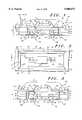
- FIG. 1is an enlarged cross-sectional view of an electronic component assembly formed in accordance with the present invention
- FIG. 2is an enlarged top view of the electronic component assembly in accordance with the present invention.
- FIG. 3is an enlarged cross-sectional view of the electronic component assembly formed in accordance with an alternate embodiment of the present invention.
- the present inventionprovides a novel process for encapsulating electronic components on a printed circuit board by flowing an encapsulation fluid over the electronic component.
- the printed circuit boardhas a solder masking layer that has a trench pattern.
- the distance that the encapsulation fluid flowsis determined by a wetting termination edge or line that is provided by the inner edge of the trench in the solder mask layer.
- the edge of the trenchprevents the encapsulation fluid from flowing into or beyond the trench and retains the encapsulation fluid within a desired area.
- the wetting termination edgesubstantially replaces the functionality provided by prior dam structures.
- FIG. 1is an enlarged cross-sectional view of an electronic component assembly 10 that comprises an electronic component 31 that is formed on a substrate 11.
- substrate 11is a printed circuit board and a bracket is used in FIG. 1 to illustrate that substrate 11 can comprise a plurality of layers.
- substrate 11can include an interconnect layer 14 sandwiched between two dielectric layers 12 and 13.
- Interconnect layer 14can contain metal traces 16 that are used to provide electrical connection between neighboring electronic components (not shown).
- Dielectric layers 12 and 13can be made from a variety of materials including: polyimide, epoxy glass, and bimaleimide-trazine (BT) resin.
- BTbimaleimide-trazine
- substrate 11could be a leadframe, a semiconductor substrate, a ceramic substrate, or similar material.
- electronic component 31can be bonded or mounted to substrate 11 using a variety of techniques known in the art and can be a semiconductor device, an integrated circuit, or an optical component.
- Dielectric layer 12 and 13have surfaces 17 and 18, respectively, upon which electronic components or electrical interconnect structures are formed.
- Vias 68 and 69are used provide electrical connection between surfaces 17 and 18 of substrate 11.
- Each via 68 and 69includes an opening that passes through dielectric layer 12, interconnect layer 14, and dielectric layer 13.
- Vias 68 and 69also include plated through holes 26 and conductive material 27 to provide electrical connection through substrate 11. As shown in FIG. 1 a portion of plated through holes 26 may be extended across surfaces 17 and 18 to provide bonding pads 38 and 39.
- Hatched markingsare used to indicate the region where plated through holes 26 exist along the surface 18 of dielectric layer 12, along the sides of vias 68 and 69 that expose portions of interconnect layer 14 and dielectric layers 12 and 13, and along the surface 17 of dielectric layer 13. Arrows are used in FIG. 1 to indicate the portion of plated through hole 26 that are referred to as bonding pads 38 and 39. Bonding pads 38 and 39 are portions of plated through holes 26. The arrows are not intended to refer to solder balls 30 that are formed on bonding pads 39 or to the wires 32 that are connected to bonding pads 38. Bonding pads 38 can be used for the placement of a bonding wire 32 that runs between each bonding pad 38 and electronic component 31. Bonding pads 39 can be used to the placement of a solder ball 30, which is electrically connected to electronic component 31. It is also possible to form other structure onto bonding pads 39 to provide electrical coupling or physical mounting to substrate 11.
- Substrate 11also includes a masking layer 21 over the surface 18 of dielectric layer 12 and a masking layer 22 over the surface 17 of dielectric layer 13.
- Masking layers 21 and 22have openings that are used to define the portions of substrate 11 that are exposed to plating processes that are used to form bonding pads 38 and 39. These openings are also used to allow bonding wires 32 or solder balls 30 to physically contact structures that are under masking layers 21 and 22.
- Masking layer 21is also referred to as a solder masking layer as it can be used to determine the placement of solder during the formation of electronic component assembly 10.
- a trench 36is formed in masking layer 21 to provide a discontinuity at a surface 23 of masking layer 21.
- Trench 36has sidewalls 37 that extend from the surface 23 to provide an edge 35.
- sidewalls 37are substantially perpendicular to the surface 23 of masking layer 21 to provide a sharp profile at the surface 23 of masking layer 21.
- sidewalls 37can be at other angles to the surface 23 as long as the profile of edge 35 of trench 36 is sufficient to halt the flow of the fluid used to form encapsulating material 33 as discussed below.
- Encapsulating material 33encases electronic component 31 and bonding wires 32 to protect these structures from the harsh environments that electronic component assembly 10 may be placed in.
- Encapsulating material 33is formed by dispensing an encapsulating fluid over electronic component 31.
- FIG. 1illustrates the final shape of the encapsulating fluid after is has been cured to provide encapsulating material 33.
- a variety of fluidscan be used to form encapsulation material 33 such as SUMIRESN EXCEL (CRP-X4095) manufactured by Sumitomo Bakelight of Tokyo, Japan.
- the encapsulation fluidAs the encapsulation fluid is dispensed onto electronic component 31, it flows across the surface 23 of masking layer 21.
- the encapsulating fluidhas an edge 41 that has a slope that provides a wetting angle 40 relative to surface 23.
- the magnitude of wetting angle 40depends on the surface tension properties of the encapsulating fluid and the cleanliness and wetting characteristics of surface 23 of masking layer 21. As shown in FIG. 1, the slope of wetting angle 40 is such that the encapsulation fluid cannot flow over the edge 35 of trench 36. Thus, the encapsulation fluid is constrained to a region defined by trench 36 around and adjacent to electronic component 31.
- trench 36has a width 34, which is preferably at least 0.5 microns, and a depth 44 that is equal to the thickness of masking layer 21.
- these dimensionsshould not be considered critical. It is possible that the width 34 of trench 36 be wider or narrower as long as the edge 35 of trench 36 is sufficient to provide a discontinuity in the surface 23 of masking layer 21 to terminate the flow of the fluid used to form encapsulating material 33. The same is true for the depth 44 of trench 36.
- trench 36passes completely through masking layer 21 and exposes a portion of dielectric layer 12. However, it is also possible to form trench 36 so that it does not completely pass through masking layer 21 as long as the depth is sufficient to provide edge 35.
- FIG. 2is an enlarged top view of electronic component assembly 10 and is used to illustrate how trench 36 is used to define the location of encapsulating material 33.
- trench 36 in masking layer 21completely encompasses electronic component 31. Therefore, the edge 35 of trench 36 provides a continuous boundary for the encapsulation fluid as it is dispensed over electronic component 31.
- trench 36need not be continuous in order to provide an effective boundary for the flow of encapsulating fluid.
- a large portion of the edge 41 (see FIG. 1) of the encapsulating fluid used to form encapsulating material 33is coincident with the edge 35 of trench 36.
- encapsulating material 33does not extend completely into the corners 62 provided by trench 36.
- a dashed line 63is used to represent the extent to which the encapsulating fluid can flow towards the edge of trench 36 near corners 62. Therefore, the edge 35 of trench 36 and the dash line 63 represent the wetting termination line for the flow of the encapsulating fluid. It should be appreciated that the configuration of trench 36 can be changed so that it is rounded in corners 62 so that the entire edge 41 of encapsulating material 33 is in contact with the edge 35 of trench 36. It is also possible to form trench 36 so that it is discontinuous in places, but due to the surface tension of the encapsulating fluid, the placement of encapsulation material 33 can be controlled. Additionally, the position of trench 36 relative to electronic component 31 can be adjusted as desired to control the size of encapsulating material 33. As indicated in FIG. 2 with bracket 60, the distance between electronic component 31 and trench 36 is preferably at least about 100 microns.
- FIG. 3is an enlarged cross-sectional view of electronic component assembly 10 that is formed with the use of a frame pattern 50 instead of a trench as discussed earlier.
- Frame pattern 50is a structure formed on the surface 23 of masking layer 21 that provides an edge 53 that is used to terminate the flow of encapsulating fluid. Due to the surface tension properties of the encapsulating fluid, the encapsulating fluid flows up the sidewalls 51 and across the upper surface 52 of the frame pattern 50. However, the flow of the encapsulating fluid terminates at the edge 53 of the frame pattern 50 because the wetting angle 40 of the encapsulating fluid is not sufficient to flow beyond frame pattern 50.
- Frame pattern 50can be formed on the surface 23 of masking layer 21 using a variety of techniques such as stamping a pattern of wax or adhesive.
- the present inventiondiffers from previously known encapsulation techniques in that a trench is formed in the upper layer of a printed circuit board to control the wettability of the printed circuit board. This in turn stops the flow of an encapsulation fluid because the wetting angle of the encapsulating fluid is too small to flow across the trench.
- previously known techniquesformed a dam structure that relies on hydrostatic equilibrium to contain an encapsulation fluid and did not use the wettability of the surface to control the flow or spreading of an encapsulation fluid.
- trench structure 36can be formed simultaneously with the formation of the other openings in masking layer 21. These other openings are typically needed to define the areas on substrate 11 that are to be exposed to plating steps, soldering steps, or other processing steps needed for the formation of printed circuit boards.
- Another advantage of the present inventionis that is does not require the formation of holes or slots that pass completely through substrate 11.
- the present inventiondoes not require any additional process steps and eliminates the process steps associated with the formation of a dam structure. Consequently the manufacturing process of electronic component assemblies in accordance with the present invention are not only cheaper, but can be done without the complexity and reliability issues associated with formation of a dam structure.
Landscapes
- Engineering & Computer Science (AREA)
- Microelectronics & Electronic Packaging (AREA)
- Computer Hardware Design (AREA)
- Power Engineering (AREA)
- Physics & Mathematics (AREA)
- Condensed Matter Physics & Semiconductors (AREA)
- General Physics & Mathematics (AREA)
- Non-Metallic Protective Coatings For Printed Circuits (AREA)
- Structures Or Materials For Encapsulating Or Coating Semiconductor Devices Or Solid State Devices (AREA)
- Encapsulation Of And Coatings For Semiconductor Or Solid State Devices (AREA)
- Production Of Multi-Layered Print Wiring Board (AREA)
Abstract
Description
Claims (14)
Priority Applications (5)
| Application Number | Priority Date | Filing Date | Title |
|---|---|---|---|
| US08/865,652US5808873A (en) | 1997-05-30 | 1997-05-30 | Electronic component assembly having an encapsulation material and method of forming the same |
| KR1019980005893AKR19980086512A (en) | 1997-05-30 | 1998-02-25 | Electronic component assembly having an encapsulating material and forming method thereof |
| CN98102142ACN1126168C (en) | 1997-05-30 | 1998-05-14 | Electronic-element assembly having package material and formation method therefor |
| JP10158423AJPH10335542A (en) | 1997-05-30 | 1998-05-22 | Electronic parts assembly having sealing material and its formation |
| MYPI98002396AMY117410A (en) | 1997-05-30 | 1998-05-29 | Electronic component assembly having an encapsulation material and method of forming the same |
Applications Claiming Priority (1)
| Application Number | Priority Date | Filing Date | Title |
|---|---|---|---|
| US08/865,652US5808873A (en) | 1997-05-30 | 1997-05-30 | Electronic component assembly having an encapsulation material and method of forming the same |
Publications (1)
| Publication Number | Publication Date |
|---|---|
| US5808873Atrue US5808873A (en) | 1998-09-15 |
Family
ID=25345964
Family Applications (1)
| Application Number | Title | Priority Date | Filing Date |
|---|---|---|---|
| US08/865,652Expired - LifetimeUS5808873A (en) | 1997-05-30 | 1997-05-30 | Electronic component assembly having an encapsulation material and method of forming the same |
Country Status (5)
| Country | Link |
|---|---|
| US (1) | US5808873A (en) |
| JP (1) | JPH10335542A (en) |
| KR (1) | KR19980086512A (en) |
| CN (1) | CN1126168C (en) |
| MY (1) | MY117410A (en) |
Cited By (79)
| Publication number | Priority date | Publication date | Assignee | Title |
|---|---|---|---|---|
| US5984691A (en)* | 1996-05-24 | 1999-11-16 | International Business Machines Corporation | Flexible circuitized interposer with apertured member and method for making same |
| US6037656A (en)* | 1996-08-12 | 2000-03-14 | Nec Corporation | Semiconductor integrated circuit device having short signal paths to terminals and process of fabrication thereof |
| US6054755A (en)* | 1997-10-14 | 2000-04-25 | Sumitomo Metal (Smi) Electronics Devices Inc. | Semiconductor package with improved moisture vapor relief function and method of fabricating the same |
| US6127728A (en)* | 1999-06-24 | 2000-10-03 | Lsi Logic Corporation | Single reference plane plastic ball grid array package |
| US6191477B1 (en)* | 1999-02-17 | 2001-02-20 | Conexant Systems, Inc. | Leadless chip carrier design and structure |
| US6215184B1 (en)* | 1998-02-19 | 2001-04-10 | Texas Instruments Incorporated | Optimized circuit design layout for high performance ball grid array packages |
| US6278177B1 (en)* | 1999-07-09 | 2001-08-21 | Samsung Electronics Co., Ltd. | Substrateless chip scale package and method of making same |
| US6351030B2 (en)* | 1997-09-29 | 2002-02-26 | International Business Machines Corporation | Electronic package utilizing protective coating |
| US6352915B1 (en) | 1997-12-30 | 2002-03-05 | Samsung Aerospace Industries, Ltd. | Method for manufacturing semiconductor package containing cylindrical type bump grid array |
| US6365979B1 (en)* | 1998-03-06 | 2002-04-02 | Kabushiki Kaisha Toshiba | Semiconductor device and manufacturing method thereof |
| US6395998B1 (en) | 2000-09-13 | 2002-05-28 | International Business Machines Corporation | Electronic package having an adhesive retaining cavity |
| US6400010B1 (en)* | 1998-02-17 | 2002-06-04 | Seiko Epson Corporation | Substrate including a metal portion and a resin portion |
| US6426565B1 (en) | 2000-03-22 | 2002-07-30 | International Business Machines Corporation | Electronic package and method of making same |
| US6448507B1 (en)* | 2000-06-28 | 2002-09-10 | Advanced Micro Devices, Inc. | Solder mask for controlling resin bleed |
| US6455926B2 (en)* | 1999-09-03 | 2002-09-24 | Thin Film Module, Inc. | High density cavity-up wire bond BGA |
| US20020134582A1 (en)* | 2001-03-26 | 2002-09-26 | Semiconductor Components Industries, Llc. | Integrated circuit package and method |
| US6469370B1 (en)* | 1999-02-23 | 2002-10-22 | Fujitsu Limited | Semiconductor device and method of production of the semiconductor device |
| US6479760B2 (en)* | 1999-02-15 | 2002-11-12 | Mitsubishi Gas Chemical Company, Inc. | Printed wiring board for semiconductor plastic package |
| US6509807B1 (en) | 1997-04-08 | 2003-01-21 | X2Y Attenuators, Llc | Energy conditioning circuit assembly |
| US6538213B1 (en)* | 2000-02-18 | 2003-03-25 | International Business Machines Corporation | High density design for organic chip carriers |
| US6582979B2 (en) | 2000-11-15 | 2003-06-24 | Skyworks Solutions, Inc. | Structure and method for fabrication of a leadless chip carrier with embedded antenna |
| US6606011B2 (en) | 1998-04-07 | 2003-08-12 | X2Y Attenuators, Llc | Energy conditioning circuit assembly |
| US6611055B1 (en) | 2000-11-15 | 2003-08-26 | Skyworks Solutions, Inc. | Leadless flip chip carrier design and structure |
| US6650525B2 (en) | 1997-04-08 | 2003-11-18 | X2Y Attenuators, Llc | Component carrier |
| US6657133B1 (en)* | 2001-05-15 | 2003-12-02 | Xilinx, Inc. | Ball grid array chip capacitor structure |
| US20040026767A1 (en)* | 2001-06-27 | 2004-02-12 | Shinko Electric Industries Co., Ltd. | Wiring substrate having position information |
| US6703689B2 (en)* | 2000-07-11 | 2004-03-09 | Seiko Epson Corporation | Miniature optical element for wireless bonding in an electronic instrument |
| US6710433B2 (en) | 2000-11-15 | 2004-03-23 | Skyworks Solutions, Inc. | Leadless chip carrier with embedded inductor |
| US20040087191A1 (en)* | 2002-11-05 | 2004-05-06 | Chih-Pin Hung | Semiconductor package with connector |
| US20040091687A1 (en)* | 2001-06-13 | 2004-05-13 | Koji Kondo | Method for manufacturing printed wiring board with embedded electric device |
| US6762509B2 (en)* | 2001-12-11 | 2004-07-13 | Celerity Research Pte. Ltd. | Flip-chip packaging method that treats an interconnect substrate to control stress created at edges of fill material |
| US20050051907A1 (en)* | 2002-09-19 | 2005-03-10 | St Assembly Test Services Ltd. | Integrated circuit package |
| US6867493B2 (en)* | 2000-11-15 | 2005-03-15 | Skyworks Solutions, Inc. | Structure and method for fabrication of a leadless multi-die carrier |
| US6873513B2 (en) | 1997-04-08 | 2005-03-29 | X2Y Attenuators, Llc | Paired multi-layered dielectric independent passive component architecture resulting in differential and common mode filtering with surge protection in one integrated package |
| US6894884B2 (en) | 1997-04-08 | 2005-05-17 | Xzy Attenuators, Llc | Offset pathway arrangements for energy conditioning |
| DE102004056449A1 (en)* | 2004-01-16 | 2005-08-25 | Continental Teves Ag & Co. Ohg | Integrated component, especially for use in motor vehicle, has protective medium with edge- and corner-free surface; protective medium has essentially square surface with rounded edges and corners |
| US6954346B2 (en) | 1997-04-08 | 2005-10-11 | Xzy Attenuators, Llc | Filter assembly |
| US6960824B1 (en) | 2000-11-15 | 2005-11-01 | Skyworks Solutions, Inc. | Structure and method for fabrication of a leadless chip carrier |
| US6995983B1 (en) | 1997-04-08 | 2006-02-07 | X2Y Attenuators, Llc | Component carrier |
| US7042703B2 (en) | 2000-03-22 | 2006-05-09 | X2Y Attenuators, Llc | Energy conditioning structure |
| US7106570B2 (en) | 1997-04-08 | 2006-09-12 | Xzy Altenuators, Llc | Pathway arrangement |
| US7110227B2 (en) | 1997-04-08 | 2006-09-19 | X2Y Attenuators, Llc | Universial energy conditioning interposer with circuit architecture |
| US7110235B2 (en) | 1997-04-08 | 2006-09-19 | Xzy Altenuators, Llc | Arrangement for energy conditioning |
| US7113383B2 (en) | 2000-04-28 | 2006-09-26 | X2Y Attenuators, Llc | Predetermined symmetrically balanced amalgam with complementary paired portions comprising shielding electrodes and shielded electrodes and other predetermined element portions for symmetrically balanced and complementary energy portion conditioning |
| US20060226202A1 (en)* | 2005-04-11 | 2006-10-12 | Ho-Ching Yang | PCB solder masking process |
| US7141899B2 (en) | 1998-04-07 | 2006-11-28 | X2Y Attenuators, Llc | Component carrier |
| US7180718B2 (en) | 2003-01-31 | 2007-02-20 | X2Y Attenuators, Llc | Shielded energy conditioner |
| US7193831B2 (en) | 2000-10-17 | 2007-03-20 | X2Y Attenuators, Llc | Energy pathway arrangement |
| US7224564B2 (en) | 2000-10-17 | 2007-05-29 | X2Y Attenuators, Llc | Amalgam of shielding and shielded energy pathways and other elements for single or multiple circuitries with common reference node |
| US20070158774A1 (en)* | 2001-10-04 | 2007-07-12 | Sony Corporation | Solid image-pickup device and method for manufacturing the solid image pickup device |
| US7262949B2 (en) | 2000-08-15 | 2007-08-28 | X2Y Attenuators, Llc | Electrode arrangement for circuit energy conditioning |
| US7274549B2 (en) | 2000-12-15 | 2007-09-25 | X2Y Attenuators, Llc | Energy pathway arrangements for energy conditioning |
| US7301748B2 (en) | 1997-04-08 | 2007-11-27 | Anthony Anthony A | Universal energy conditioning interposer with circuit architecture |
| US7321485B2 (en) | 1997-04-08 | 2008-01-22 | X2Y Attenuators, Llc | Arrangement for energy conditioning |
| US7336467B2 (en) | 2000-10-17 | 2008-02-26 | X2Y Attenuators, Llc | Energy pathway arrangement |
| US7336468B2 (en) | 1997-04-08 | 2008-02-26 | X2Y Attenuators, Llc | Arrangement for energy conditioning |
| DE102006059127A1 (en)* | 2006-09-25 | 2008-03-27 | Osram Opto Semiconductors Gmbh | Method for production of arrangement of optoelectronic components, involves manufacturing two attachment areas on connection carrier and bringing soldering material into attachment areas |
| US7423860B2 (en) | 1997-04-08 | 2008-09-09 | X2Y Attenuators, Llc | Multi-functional energy conditioner |
| US7427816B2 (en) | 1998-04-07 | 2008-09-23 | X2Y Attenuators, Llc | Component carrier |
| US7429799B1 (en) | 2005-07-27 | 2008-09-30 | Amkor Technology, Inc. | Land patterns for a semiconductor stacking structure and method therefor |
| US7440252B2 (en) | 2003-05-29 | 2008-10-21 | X2Y Attenuators, Llc | Connector related structures including an energy conditioner |
| US20080258285A1 (en)* | 2007-04-23 | 2008-10-23 | Texas Instruments Incorporated | Simplified Substrates for Semiconductor Devices in Package-on-Package Products |
| US7443647B2 (en) | 1997-04-08 | 2008-10-28 | X2Y Attenuators, Llc | Paired multi-layered dielectric independent passive component architecture resulting in differential and common mode filtering with surge protection in one integrated package |
| US20080304821A1 (en)* | 2007-06-05 | 2008-12-11 | Samsung Electro-Mechanics Co., Ltd. | Camera module package and method of manufacturing the same |
| US20090107701A1 (en)* | 2007-10-24 | 2009-04-30 | Samsung Electronics Co., Ltd. | Printed circuit board having adhesive layer and semiconductor package using the same |
| US7586728B2 (en) | 2005-03-14 | 2009-09-08 | X2Y Attenuators, Llc | Conditioner with coplanar conductors |
| US7630188B2 (en) | 2005-03-01 | 2009-12-08 | X2Y Attenuators, Llc | Conditioner with coplanar conductors |
| US7675729B2 (en) | 2003-12-22 | 2010-03-09 | X2Y Attenuators, Llc | Internally shielded energy conditioner |
| US20100213592A1 (en)* | 2009-02-24 | 2010-08-26 | International Business Machines Corporation | Semiconductor Module, Terminal Strip, Method for Manufacturing Terminal Strip, and Method for Manufacturing Semiconductor Module |
| US7817397B2 (en) | 2005-03-01 | 2010-10-19 | X2Y Attenuators, Llc | Energy conditioner with tied through electrodes |
| US20110115918A1 (en)* | 1999-12-08 | 2011-05-19 | Amkor Technology, Inc. | Camera module having lens mount with ir filter |
| US20110127636A1 (en)* | 2009-11-27 | 2011-06-02 | Samsung Electro-Mechanics Co., Ltd. | Integrated passive device assembly |
| US20110205719A1 (en)* | 2010-02-24 | 2011-08-25 | Atsushi Watanabe | Electronic component |
| US8026777B2 (en) | 2006-03-07 | 2011-09-27 | X2Y Attenuators, Llc | Energy conditioner structures |
| US20110290545A1 (en)* | 2004-03-26 | 2011-12-01 | Fujikura Ltd. | Through wiring board and method of manufacturing the same |
| US20120193802A1 (en)* | 2011-02-01 | 2012-08-02 | Chin-Tien Chiu | Glob top semiconductor package |
| US8415785B1 (en)* | 2010-01-27 | 2013-04-09 | Marvell International Ltd. | Metal ring techniques and configurations |
| US9054094B2 (en) | 1997-04-08 | 2015-06-09 | X2Y Attenuators, Llc | Energy conditioning circuit arrangement for integrated circuit |
| US20220287185A1 (en)* | 2019-08-22 | 2022-09-08 | Stemco Co., Ltd. | Circuit board and manufacturing method therefor |
Families Citing this family (3)
| Publication number | Priority date | Publication date | Assignee | Title |
|---|---|---|---|---|
| CN101370361B (en)* | 2001-06-13 | 2010-09-08 | 株式会社电装 | Method for manufacturing printed wiring board with embedded electric device |
| CN100431140C (en)* | 2002-03-21 | 2008-11-05 | Nxp股份有限公司 | Semiconductor device with protective security coating and method of manufacturing the same |
| JP6111832B2 (en)* | 2013-05-06 | 2017-04-12 | 株式会社デンソー | Multilayer substrate, electronic device using the same, and method for manufacturing electronic device |
Citations (5)
| Publication number | Priority date | Publication date | Assignee | Title |
|---|---|---|---|---|
| US5239198A (en)* | 1989-09-06 | 1993-08-24 | Motorola, Inc. | Overmolded semiconductor device having solder ball and edge lead connective structure |
| US5455456A (en)* | 1993-09-15 | 1995-10-03 | Lsi Logic Corporation | Integrated circuit package lid |
| US5468999A (en)* | 1994-05-26 | 1995-11-21 | Motorola, Inc. | Liquid encapsulated ball grid array semiconductor device with fine pitch wire bonding |
| US5468784A (en)* | 1994-02-23 | 1995-11-21 | Tamura Kaken Corporation | Photopolymerizable resin composition |
| US5652463A (en)* | 1995-05-26 | 1997-07-29 | Hestia Technologies, Inc. | Transfer modlded electronic package having a passage means |
- 1997
- 1997-05-30USUS08/865,652patent/US5808873A/ennot_activeExpired - Lifetime
- 1998
- 1998-02-25KRKR1019980005893Apatent/KR19980086512A/ennot_activeCeased
- 1998-05-14CNCN98102142Apatent/CN1126168C/ennot_activeExpired - Fee Related
- 1998-05-22JPJP10158423Apatent/JPH10335542A/enactivePending
- 1998-05-29MYMYPI98002396Apatent/MY117410A/enunknown
Patent Citations (5)
| Publication number | Priority date | Publication date | Assignee | Title |
|---|---|---|---|---|
| US5239198A (en)* | 1989-09-06 | 1993-08-24 | Motorola, Inc. | Overmolded semiconductor device having solder ball and edge lead connective structure |
| US5455456A (en)* | 1993-09-15 | 1995-10-03 | Lsi Logic Corporation | Integrated circuit package lid |
| US5468784A (en)* | 1994-02-23 | 1995-11-21 | Tamura Kaken Corporation | Photopolymerizable resin composition |
| US5468999A (en)* | 1994-05-26 | 1995-11-21 | Motorola, Inc. | Liquid encapsulated ball grid array semiconductor device with fine pitch wire bonding |
| US5652463A (en)* | 1995-05-26 | 1997-07-29 | Hestia Technologies, Inc. | Transfer modlded electronic package having a passage means |
Cited By (135)
| Publication number | Priority date | Publication date | Assignee | Title |
|---|---|---|---|---|
| US5984691A (en)* | 1996-05-24 | 1999-11-16 | International Business Machines Corporation | Flexible circuitized interposer with apertured member and method for making same |
| US6037656A (en)* | 1996-08-12 | 2000-03-14 | Nec Corporation | Semiconductor integrated circuit device having short signal paths to terminals and process of fabrication thereof |
| US7106570B2 (en) | 1997-04-08 | 2006-09-12 | Xzy Altenuators, Llc | Pathway arrangement |
| US6509807B1 (en) | 1997-04-08 | 2003-01-21 | X2Y Attenuators, Llc | Energy conditioning circuit assembly |
| US7301748B2 (en) | 1997-04-08 | 2007-11-27 | Anthony Anthony A | Universal energy conditioning interposer with circuit architecture |
| US7321485B2 (en) | 1997-04-08 | 2008-01-22 | X2Y Attenuators, Llc | Arrangement for energy conditioning |
| US7336468B2 (en) | 1997-04-08 | 2008-02-26 | X2Y Attenuators, Llc | Arrangement for energy conditioning |
| US8018706B2 (en) | 1997-04-08 | 2011-09-13 | X2Y Attenuators, Llc | Arrangement for energy conditioning |
| US7768763B2 (en) | 1997-04-08 | 2010-08-03 | X2Y Attenuators, Llc | Arrangement for energy conditioning |
| US7423860B2 (en) | 1997-04-08 | 2008-09-09 | X2Y Attenuators, Llc | Multi-functional energy conditioner |
| US7443647B2 (en) | 1997-04-08 | 2008-10-28 | X2Y Attenuators, Llc | Paired multi-layered dielectric independent passive component architecture resulting in differential and common mode filtering with surge protection in one integrated package |
| US7916444B2 (en) | 1997-04-08 | 2011-03-29 | X2Y Attenuators, Llc | Arrangement for energy conditioning |
| US7110235B2 (en) | 1997-04-08 | 2006-09-19 | Xzy Altenuators, Llc | Arrangement for energy conditioning |
| US7110227B2 (en) | 1997-04-08 | 2006-09-19 | X2Y Attenuators, Llc | Universial energy conditioning interposer with circuit architecture |
| US7050284B2 (en) | 1997-04-08 | 2006-05-23 | X2Y Attenuators, Llc | Component carrier |
| US6995983B1 (en) | 1997-04-08 | 2006-02-07 | X2Y Attenuators, Llc | Component carrier |
| US7593208B2 (en) | 1997-04-08 | 2009-09-22 | X2Y Attenuators, Llc | Multi-functional energy conditioner |
| US7609501B2 (en) | 1997-04-08 | 2009-10-27 | X2Y Attenuators, Llc | Manufacture including shield structure |
| US7609500B2 (en) | 1997-04-08 | 2009-10-27 | X2Y Attenuators, Llc | Universal energy conditioning interposer with circuit architecture |
| US8004812B2 (en) | 1997-04-08 | 2011-08-23 | X2Y Attenuators, Llc | Energy conditioning circuit arrangement for integrated circuit |
| US6954346B2 (en) | 1997-04-08 | 2005-10-11 | Xzy Attenuators, Llc | Filter assembly |
| US9373592B2 (en) | 1997-04-08 | 2016-06-21 | X2Y Attenuators, Llc | Arrangement for energy conditioning |
| US7688565B2 (en) | 1997-04-08 | 2010-03-30 | X2Y Attenuators, Llc | Arrangements for energy conditioning |
| US7733621B2 (en) | 1997-04-08 | 2010-06-08 | X2Y Attenuators, Llc | Energy conditioning circuit arrangement for integrated circuit |
| US7920367B2 (en) | 1997-04-08 | 2011-04-05 | X2Y Attenuators, Llc | Method for making arrangement for energy conditioning |
| US6650525B2 (en) | 1997-04-08 | 2003-11-18 | X2Y Attenuators, Llc | Component carrier |
| US9054094B2 (en) | 1997-04-08 | 2015-06-09 | X2Y Attenuators, Llc | Energy conditioning circuit arrangement for integrated circuit |
| US9036319B2 (en) | 1997-04-08 | 2015-05-19 | X2Y Attenuators, Llc | Arrangement for energy conditioning |
| US6894884B2 (en) | 1997-04-08 | 2005-05-17 | Xzy Attenuators, Llc | Offset pathway arrangements for energy conditioning |
| US9019679B2 (en) | 1997-04-08 | 2015-04-28 | X2Y Attenuators, Llc | Arrangement for energy conditioning |
| US6873513B2 (en) | 1997-04-08 | 2005-03-29 | X2Y Attenuators, Llc | Paired multi-layered dielectric independent passive component architecture resulting in differential and common mode filtering with surge protection in one integrated package |
| US8587915B2 (en) | 1997-04-08 | 2013-11-19 | X2Y Attenuators, Llc | Arrangement for energy conditioning |
| US8023241B2 (en) | 1997-04-08 | 2011-09-20 | X2Y Attenuators, Llc | Arrangement for energy conditioning |
| US6351030B2 (en)* | 1997-09-29 | 2002-02-26 | International Business Machines Corporation | Electronic package utilizing protective coating |
| US6054755A (en)* | 1997-10-14 | 2000-04-25 | Sumitomo Metal (Smi) Electronics Devices Inc. | Semiconductor package with improved moisture vapor relief function and method of fabricating the same |
| US6352915B1 (en) | 1997-12-30 | 2002-03-05 | Samsung Aerospace Industries, Ltd. | Method for manufacturing semiconductor package containing cylindrical type bump grid array |
| US6400010B1 (en)* | 1998-02-17 | 2002-06-04 | Seiko Epson Corporation | Substrate including a metal portion and a resin portion |
| US6586274B2 (en) | 1998-02-17 | 2003-07-01 | Seiko Epson Corporation | Semiconductor device, substrate for a semiconductor device, method of manufacture thereof, and electronic instrument |
| US6215184B1 (en)* | 1998-02-19 | 2001-04-10 | Texas Instruments Incorporated | Optimized circuit design layout for high performance ball grid array packages |
| US6365979B1 (en)* | 1998-03-06 | 2002-04-02 | Kabushiki Kaisha Toshiba | Semiconductor device and manufacturing method thereof |
| US7427816B2 (en) | 1998-04-07 | 2008-09-23 | X2Y Attenuators, Llc | Component carrier |
| US7141899B2 (en) | 1998-04-07 | 2006-11-28 | X2Y Attenuators, Llc | Component carrier |
| US6606011B2 (en) | 1998-04-07 | 2003-08-12 | X2Y Attenuators, Llc | Energy conditioning circuit assembly |
| US7042303B2 (en) | 1998-04-07 | 2006-05-09 | X2Y Attenuators, Llc | Energy conditioning circuit assembly |
| US6479760B2 (en)* | 1999-02-15 | 2002-11-12 | Mitsubishi Gas Chemical Company, Inc. | Printed wiring board for semiconductor plastic package |
| US6191477B1 (en)* | 1999-02-17 | 2001-02-20 | Conexant Systems, Inc. | Leadless chip carrier design and structure |
| US6921972B1 (en)* | 1999-02-17 | 2005-07-26 | Skyworks Solutions, Inc. | Leadless chip carrier design and structure |
| US6469370B1 (en)* | 1999-02-23 | 2002-10-22 | Fujitsu Limited | Semiconductor device and method of production of the semiconductor device |
| US6127728A (en)* | 1999-06-24 | 2000-10-03 | Lsi Logic Corporation | Single reference plane plastic ball grid array package |
| US6396140B1 (en)* | 1999-06-24 | 2002-05-28 | Lsi Logic Corporation | Single reference plane plastic ball grid array package |
| US6278177B1 (en)* | 1999-07-09 | 2001-08-21 | Samsung Electronics Co., Ltd. | Substrateless chip scale package and method of making same |
| US6455926B2 (en)* | 1999-09-03 | 2002-09-24 | Thin Film Module, Inc. | High density cavity-up wire bond BGA |
| US9735191B2 (en) | 1999-12-08 | 2017-08-15 | Amkor Technology, Inc. | Molded semiconductor package |
| US9332164B2 (en) | 1999-12-08 | 2016-05-03 | Amkor Technology, Inc. | Molded semiconductor package with snap lid |
| US20110115918A1 (en)* | 1999-12-08 | 2011-05-19 | Amkor Technology, Inc. | Camera module having lens mount with ir filter |
| US8994860B2 (en) | 1999-12-08 | 2015-03-31 | Amkor, Technology, Inc. | Molded image sensor package and method |
| US6538213B1 (en)* | 2000-02-18 | 2003-03-25 | International Business Machines Corporation | High density design for organic chip carriers |
| US7042703B2 (en) | 2000-03-22 | 2006-05-09 | X2Y Attenuators, Llc | Energy conditioning structure |
| US6426565B1 (en) | 2000-03-22 | 2002-07-30 | International Business Machines Corporation | Electronic package and method of making same |
| US7113383B2 (en) | 2000-04-28 | 2006-09-26 | X2Y Attenuators, Llc | Predetermined symmetrically balanced amalgam with complementary paired portions comprising shielding electrodes and shielded electrodes and other predetermined element portions for symmetrically balanced and complementary energy portion conditioning |
| US6448507B1 (en)* | 2000-06-28 | 2002-09-10 | Advanced Micro Devices, Inc. | Solder mask for controlling resin bleed |
| US7074632B2 (en) | 2000-07-11 | 2006-07-11 | Seiko Epson Corporation | Miniature optical element for wireless bonding in an electronic instrument |
| US7544973B2 (en) | 2000-07-11 | 2009-06-09 | Seiko Epson Corporation | Miniature optical element for wireless bonding in an electronic instrument |
| US20090221108A1 (en)* | 2000-07-11 | 2009-09-03 | Seiko Epson Corporation | Miniature optical element for wireless bonding in an electronic instrument |
| US20060208331A1 (en)* | 2000-07-11 | 2006-09-21 | Seiko Epson Corporation | Miniature optical element for wireless bonding in an electronic instrument |
| US20080009087A1 (en)* | 2000-07-11 | 2008-01-10 | Seiko Epson Corporation | Miniature optical element for wireless bonding in an electronic instrument |
| US6703689B2 (en)* | 2000-07-11 | 2004-03-09 | Seiko Epson Corporation | Miniature optical element for wireless bonding in an electronic instrument |
| US7879633B2 (en) | 2000-07-11 | 2011-02-01 | Seiko Epson Corporation | Miniature optical element for wireless bonding in an electronic instrument |
| US7276738B2 (en) | 2000-07-11 | 2007-10-02 | Seiko Epson Corporation | Miniature optical element for wireless bonding in an electronic instrument |
| US20040147051A1 (en)* | 2000-07-11 | 2004-07-29 | Seiko Epson Corporation | Miniature optical element for wireless bonding in an electronic instrument |
| US7262949B2 (en) | 2000-08-15 | 2007-08-28 | X2Y Attenuators, Llc | Electrode arrangement for circuit energy conditioning |
| US6395998B1 (en) | 2000-09-13 | 2002-05-28 | International Business Machines Corporation | Electronic package having an adhesive retaining cavity |
| US7224564B2 (en) | 2000-10-17 | 2007-05-29 | X2Y Attenuators, Llc | Amalgam of shielding and shielded energy pathways and other elements for single or multiple circuitries with common reference node |
| US7336467B2 (en) | 2000-10-17 | 2008-02-26 | X2Y Attenuators, Llc | Energy pathway arrangement |
| US7193831B2 (en) | 2000-10-17 | 2007-03-20 | X2Y Attenuators, Llc | Energy pathway arrangement |
| US7428134B2 (en) | 2000-10-17 | 2008-09-23 | X2Y Attenuators, Llc | Energy pathway arrangements for energy conditioning |
| US7433168B2 (en) | 2000-10-17 | 2008-10-07 | X2Y Attenuators, Llc | Amalgam of shielding and shielded energy pathways and other elements for single or multiple circuitries with common reference node |
| US6611055B1 (en) | 2000-11-15 | 2003-08-26 | Skyworks Solutions, Inc. | Leadless flip chip carrier design and structure |
| US6867493B2 (en)* | 2000-11-15 | 2005-03-15 | Skyworks Solutions, Inc. | Structure and method for fabrication of a leadless multi-die carrier |
| US6960824B1 (en) | 2000-11-15 | 2005-11-01 | Skyworks Solutions, Inc. | Structure and method for fabrication of a leadless chip carrier |
| US6582979B2 (en) | 2000-11-15 | 2003-06-24 | Skyworks Solutions, Inc. | Structure and method for fabrication of a leadless chip carrier with embedded antenna |
| US6710433B2 (en) | 2000-11-15 | 2004-03-23 | Skyworks Solutions, Inc. | Leadless chip carrier with embedded inductor |
| US7274549B2 (en) | 2000-12-15 | 2007-09-25 | X2Y Attenuators, Llc | Energy pathway arrangements for energy conditioning |
| US6889429B2 (en)* | 2001-03-26 | 2005-05-10 | Semiconductor Components Industries, L.L.C. | Method of making a lead-free integrated circuit package |
| US20020134582A1 (en)* | 2001-03-26 | 2002-09-26 | Semiconductor Components Industries, Llc. | Integrated circuit package and method |
| US20050121767A1 (en)* | 2001-03-26 | 2005-06-09 | Celaya Phillip C. | Integrated circuit package and method |
| US7180170B2 (en)* | 2001-03-26 | 2007-02-20 | Semiconductor Components Industries, L.L.C. | Lead-free integrated circuit package structure |
| US6657133B1 (en)* | 2001-05-15 | 2003-12-02 | Xilinx, Inc. | Ball grid array chip capacitor structure |
| US7165321B2 (en) | 2001-06-13 | 2007-01-23 | Denso Corporation | Method for manufacturing printed wiring board with embedded electric device |
| US20040091687A1 (en)* | 2001-06-13 | 2004-05-13 | Koji Kondo | Method for manufacturing printed wiring board with embedded electric device |
| US6861764B2 (en)* | 2001-06-27 | 2005-03-01 | Shinko Electric Industries Co., Ltd. | Wiring substrate having position information |
| US6855626B2 (en) | 2001-06-27 | 2005-02-15 | Shinko Electric Industries Co., Ltd. | Wiring substrate having position information |
| US20040026767A1 (en)* | 2001-06-27 | 2004-02-12 | Shinko Electric Industries Co., Ltd. | Wiring substrate having position information |
| US8410567B2 (en)* | 2001-10-04 | 2013-04-02 | Sony Corporation | Solid image-pickup device with flexible circuit substrate |
| US20070158774A1 (en)* | 2001-10-04 | 2007-07-12 | Sony Corporation | Solid image-pickup device and method for manufacturing the solid image pickup device |
| US20040178515A1 (en)* | 2001-12-11 | 2004-09-16 | Hilton Robert M. | Flip-chip package with underfill dam for stress control |
| US6940182B2 (en) | 2001-12-11 | 2005-09-06 | Celerity Research Pte. Ltd. | Flip-chip package with underfill dam for stress control |
| US6762509B2 (en)* | 2001-12-11 | 2004-07-13 | Celerity Research Pte. Ltd. | Flip-chip packaging method that treats an interconnect substrate to control stress created at edges of fill material |
| US6979907B2 (en)* | 2002-09-19 | 2005-12-27 | St Assembly Test Services Ltd. | Integrated circuit package |
| US20050051907A1 (en)* | 2002-09-19 | 2005-03-10 | St Assembly Test Services Ltd. | Integrated circuit package |
| US6974334B2 (en)* | 2002-11-05 | 2005-12-13 | Advanced Semiconductor Engineering, Inc. | Semiconductor package with connector |
| US20040087191A1 (en)* | 2002-11-05 | 2004-05-06 | Chih-Pin Hung | Semiconductor package with connector |
| US7180718B2 (en) | 2003-01-31 | 2007-02-20 | X2Y Attenuators, Llc | Shielded energy conditioner |
| US7440252B2 (en) | 2003-05-29 | 2008-10-21 | X2Y Attenuators, Llc | Connector related structures including an energy conditioner |
| US7675729B2 (en) | 2003-12-22 | 2010-03-09 | X2Y Attenuators, Llc | Internally shielded energy conditioner |
| DE102004056449A1 (en)* | 2004-01-16 | 2005-08-25 | Continental Teves Ag & Co. Ohg | Integrated component, especially for use in motor vehicle, has protective medium with edge- and corner-free surface; protective medium has essentially square surface with rounded edges and corners |
| US20110290545A1 (en)* | 2004-03-26 | 2011-12-01 | Fujikura Ltd. | Through wiring board and method of manufacturing the same |
| US8547677B2 (en) | 2005-03-01 | 2013-10-01 | X2Y Attenuators, Llc | Method for making internally overlapped conditioners |
| US7974062B2 (en) | 2005-03-01 | 2011-07-05 | X2Y Attenuators, Llc | Internally overlapped conditioners |
| US7782587B2 (en) | 2005-03-01 | 2010-08-24 | X2Y Attenuators, Llc | Internally overlapped conditioners |
| US7630188B2 (en) | 2005-03-01 | 2009-12-08 | X2Y Attenuators, Llc | Conditioner with coplanar conductors |
| US8014119B2 (en) | 2005-03-01 | 2011-09-06 | X2Y Attenuators, Llc | Energy conditioner with tied through electrodes |
| US9001486B2 (en) | 2005-03-01 | 2015-04-07 | X2Y Attenuators, Llc | Internally overlapped conditioners |
| US7817397B2 (en) | 2005-03-01 | 2010-10-19 | X2Y Attenuators, Llc | Energy conditioner with tied through electrodes |
| US7586728B2 (en) | 2005-03-14 | 2009-09-08 | X2Y Attenuators, Llc | Conditioner with coplanar conductors |
| US20060226202A1 (en)* | 2005-04-11 | 2006-10-12 | Ho-Ching Yang | PCB solder masking process |
| US7429799B1 (en) | 2005-07-27 | 2008-09-30 | Amkor Technology, Inc. | Land patterns for a semiconductor stacking structure and method therefor |
| US7691745B1 (en) | 2005-07-27 | 2010-04-06 | Amkor Technology, Inc. | Land patterns for a semiconductor stacking structure and method therefor |
| US8026777B2 (en) | 2006-03-07 | 2011-09-27 | X2Y Attenuators, Llc | Energy conditioner structures |
| US8638565B2 (en) | 2006-09-25 | 2014-01-28 | Osram Opto Semiconductors Gmbh | Arrangement of optoelectronic components |
| DE102006059127A1 (en)* | 2006-09-25 | 2008-03-27 | Osram Opto Semiconductors Gmbh | Method for production of arrangement of optoelectronic components, involves manufacturing two attachment areas on connection carrier and bringing soldering material into attachment areas |
| US20100079964A1 (en)* | 2006-09-25 | 2010-04-01 | Osram Semiconductors Gmbh | Method for Producing an Arrangement of Optoelectronic Components, and Arrangement of Optoelectronic Components |
| US20080258285A1 (en)* | 2007-04-23 | 2008-10-23 | Texas Instruments Incorporated | Simplified Substrates for Semiconductor Devices in Package-on-Package Products |
| US20080304821A1 (en)* | 2007-06-05 | 2008-12-11 | Samsung Electro-Mechanics Co., Ltd. | Camera module package and method of manufacturing the same |
| US20090107701A1 (en)* | 2007-10-24 | 2009-04-30 | Samsung Electronics Co., Ltd. | Printed circuit board having adhesive layer and semiconductor package using the same |
| US20100213592A1 (en)* | 2009-02-24 | 2010-08-26 | International Business Machines Corporation | Semiconductor Module, Terminal Strip, Method for Manufacturing Terminal Strip, and Method for Manufacturing Semiconductor Module |
| US20110127636A1 (en)* | 2009-11-27 | 2011-06-02 | Samsung Electro-Mechanics Co., Ltd. | Integrated passive device assembly |
| US8749045B1 (en) | 2010-01-27 | 2014-06-10 | Marvell International Ltd. | Metal ring techniques and configurations |
| US8415785B1 (en)* | 2010-01-27 | 2013-04-09 | Marvell International Ltd. | Metal ring techniques and configurations |
| US8867227B2 (en)* | 2010-02-24 | 2014-10-21 | Panasonic Corporation | Electronic component |
| US20110205719A1 (en)* | 2010-02-24 | 2011-08-25 | Atsushi Watanabe | Electronic component |
| CN102194787A (en)* | 2010-02-24 | 2011-09-21 | 松下电器产业株式会社 | Electronic component |
| US20120193802A1 (en)* | 2011-02-01 | 2012-08-02 | Chin-Tien Chiu | Glob top semiconductor package |
| US20220287185A1 (en)* | 2019-08-22 | 2022-09-08 | Stemco Co., Ltd. | Circuit board and manufacturing method therefor |
| US12256500B2 (en)* | 2019-08-22 | 2025-03-18 | Stemco Co., Ltd. | Circuit board and manufacturing method therefor |
Also Published As
| Publication number | Publication date |
|---|---|
| CN1126168C (en) | 2003-10-29 |
| KR19980086512A (en) | 1998-12-05 |
| CN1201255A (en) | 1998-12-09 |
| JPH10335542A (en) | 1998-12-18 |
| MY117410A (en) | 2004-06-30 |
Similar Documents
| Publication | Publication Date | Title |
|---|---|---|
| US5808873A (en) | Electronic component assembly having an encapsulation material and method of forming the same | |
| US6528869B1 (en) | Semiconductor package with molded substrate and recessed input/output terminals | |
| US6787923B2 (en) | Solder masks for use on carrier substrates, carrier substrates and semiconductor device assemblies including such solder masks | |
| US6210992B1 (en) | Controlling packaging encapsulant leakage | |
| KR950012658B1 (en) | Semiconductor chip mounting method and substrate structure | |
| US5936847A (en) | Low profile electronic circuit modules | |
| KR20030024620A (en) | A semiconductor device and method of manufacturing the same | |
| US9355992B2 (en) | Land grid array semiconductor device packages | |
| KR100449307B1 (en) | Semiconductor device and method for manufacturing the same | |
| US6081426A (en) | Semiconductor package having a heat slug | |
| US6246124B1 (en) | Encapsulated chip module and method of making same | |
| KR100788858B1 (en) | Structure and assembly method of integrated circuit package | |
| KR20160020832A (en) | Printed citcuit board and Semiconductor package using the same | |
| US7368391B2 (en) | Methods for designing carrier substrates with raised terminals | |
| KR100829613B1 (en) | Semiconductor chip package and manufacturing method thereof | |
| JP2797598B2 (en) | Hybrid integrated circuit board | |
| KR20010067308A (en) | Integrated circuit package with stacked dies | |
| HK1016345A (en) | Electronic component assembly having an encapsulation material and method of forming the same | |
| KR980012301A (en) | Electronic components and how to encapsulate them in a package | |
| KR100727246B1 (en) | Semiconductor package | |
| KR100668939B1 (en) | Board level semiconductor device and manufacturing method thereof | |
| KR100743319B1 (en) | Surface-mounted semiconductor device and manufacturing method thereof | |
| JPH03283552A (en) | hybrid integrated circuit board | |
| JPH03254134A (en) | Resin seal of electric components | |
| KR100729081B1 (en) | Semiconductor package and manufacturing method |
Legal Events
| Date | Code | Title | Description |
|---|---|---|---|
| AS | Assignment | Owner name:MOTOROLA, INC., ILLINOIS Free format text:ASSIGNMENT OF ASSIGNORS INTEREST;ASSIGNORS:CELAYA, PHILLIP C.;KERR, JOHN R.;REEL/FRAME:009306/0449 Effective date:19970529 | |
| STCF | Information on status: patent grant | Free format text:PATENTED CASE | |
| FPAY | Fee payment | Year of fee payment:4 | |
| AS | Assignment | Owner name:FREESCALE SEMICONDUCTOR, INC., TEXAS Free format text:ASSIGNMENT OF ASSIGNORS INTEREST;ASSIGNOR:MOTOROLA, INC.;REEL/FRAME:015698/0657 Effective date:20040404 Owner name:FREESCALE SEMICONDUCTOR, INC.,TEXAS Free format text:ASSIGNMENT OF ASSIGNORS INTEREST;ASSIGNOR:MOTOROLA, INC.;REEL/FRAME:015698/0657 Effective date:20040404 | |
| FPAY | Fee payment | Year of fee payment:8 | |
| AS | Assignment | Owner name:CITIBANK, N.A. AS COLLATERAL AGENT, NEW YORK Free format text:SECURITY AGREEMENT;ASSIGNORS:FREESCALE SEMICONDUCTOR, INC.;FREESCALE ACQUISITION CORPORATION;FREESCALE ACQUISITION HOLDINGS CORP.;AND OTHERS;REEL/FRAME:018855/0129 Effective date:20061201 Owner name:CITIBANK, N.A. AS COLLATERAL AGENT,NEW YORK Free format text:SECURITY AGREEMENT;ASSIGNORS:FREESCALE SEMICONDUCTOR, INC.;FREESCALE ACQUISITION CORPORATION;FREESCALE ACQUISITION HOLDINGS CORP.;AND OTHERS;REEL/FRAME:018855/0129 Effective date:20061201 | |
| FPAY | Fee payment | Year of fee payment:12 | |
| AS | Assignment | Owner name:CITIBANK, N.A., AS COLLATERAL AGENT,NEW YORK Free format text:SECURITY AGREEMENT;ASSIGNOR:FREESCALE SEMICONDUCTOR, INC.;REEL/FRAME:024397/0001 Effective date:20100413 Owner name:CITIBANK, N.A., AS COLLATERAL AGENT, NEW YORK Free format text:SECURITY AGREEMENT;ASSIGNOR:FREESCALE SEMICONDUCTOR, INC.;REEL/FRAME:024397/0001 Effective date:20100413 | |
| AS | Assignment | Owner name:CITIBANK, N.A., AS NOTES COLLATERAL AGENT, NEW YORK Free format text:SECURITY AGREEMENT;ASSIGNOR:FREESCALE SEMICONDUCTOR, INC.;REEL/FRAME:030633/0424 Effective date:20130521 Owner name:CITIBANK, N.A., AS NOTES COLLATERAL AGENT, NEW YOR Free format text:SECURITY AGREEMENT;ASSIGNOR:FREESCALE SEMICONDUCTOR, INC.;REEL/FRAME:030633/0424 Effective date:20130521 | |
| AS | Assignment | Owner name:CITIBANK, N.A., AS NOTES COLLATERAL AGENT, NEW YORK Free format text:SECURITY AGREEMENT;ASSIGNOR:FREESCALE SEMICONDUCTOR, INC.;REEL/FRAME:031591/0266 Effective date:20131101 Owner name:CITIBANK, N.A., AS NOTES COLLATERAL AGENT, NEW YOR Free format text:SECURITY AGREEMENT;ASSIGNOR:FREESCALE SEMICONDUCTOR, INC.;REEL/FRAME:031591/0266 Effective date:20131101 | |
| AS | Assignment | Owner name:FREESCALE SEMICONDUCTOR, INC., TEXAS Free format text:PATENT RELEASE;ASSIGNOR:CITIBANK, N.A., AS COLLATERAL AGENT;REEL/FRAME:037356/0553 Effective date:20151207 Owner name:FREESCALE SEMICONDUCTOR, INC., TEXAS Free format text:PATENT RELEASE;ASSIGNOR:CITIBANK, N.A., AS COLLATERAL AGENT;REEL/FRAME:037356/0143 Effective date:20151207 Owner name:FREESCALE SEMICONDUCTOR, INC., TEXAS Free format text:PATENT RELEASE;ASSIGNOR:CITIBANK, N.A., AS COLLATERAL AGENT;REEL/FRAME:037354/0225 Effective date:20151207 | |
| AS | Assignment | Owner name:MORGAN STANLEY SENIOR FUNDING, INC., MARYLAND Free format text:ASSIGNMENT AND ASSUMPTION OF SECURITY INTEREST IN PATENTS;ASSIGNOR:CITIBANK, N.A.;REEL/FRAME:037486/0517 Effective date:20151207 | |
| AS | Assignment | Owner name:MORGAN STANLEY SENIOR FUNDING, INC., MARYLAND Free format text:ASSIGNMENT AND ASSUMPTION OF SECURITY INTEREST IN PATENTS;ASSIGNOR:CITIBANK, N.A.;REEL/FRAME:037518/0292 Effective date:20151207 | |
| AS | Assignment | Owner name:MORGAN STANLEY SENIOR FUNDING, INC., MARYLAND Free format text:SUPPLEMENT TO THE SECURITY AGREEMENT;ASSIGNOR:FREESCALE SEMICONDUCTOR, INC.;REEL/FRAME:039138/0001 Effective date:20160525 | |
| AS | Assignment | Owner name:NXP, B.V., F/K/A FREESCALE SEMICONDUCTOR, INC., NETHERLANDS Free format text:RELEASE BY SECURED PARTY;ASSIGNOR:MORGAN STANLEY SENIOR FUNDING, INC.;REEL/FRAME:040925/0001 Effective date:20160912 Owner name:NXP, B.V., F/K/A FREESCALE SEMICONDUCTOR, INC., NE Free format text:RELEASE BY SECURED PARTY;ASSIGNOR:MORGAN STANLEY SENIOR FUNDING, INC.;REEL/FRAME:040925/0001 Effective date:20160912 | |
| AS | Assignment | Owner name:NXP B.V., NETHERLANDS Free format text:RELEASE BY SECURED PARTY;ASSIGNOR:MORGAN STANLEY SENIOR FUNDING, INC.;REEL/FRAME:040928/0001 Effective date:20160622 | |
| AS | Assignment | Owner name:NXP USA, INC., TEXAS Free format text:CHANGE OF NAME;ASSIGNOR:FREESCALE SEMICONDUCTOR, INC.;REEL/FRAME:040652/0241 Effective date:20161107 Owner name:NXP USA, INC., TEXAS Free format text:MERGER;ASSIGNOR:FREESCALE SEMICONDUCTOR, INC.;REEL/FRAME:040652/0241 Effective date:20161107 | |
| AS | Assignment | Owner name:NXP USA, INC., TEXAS Free format text:CORRECTIVE ASSIGNMENT TO CORRECT THE NATURE OF CONVEYANCE PREVIOUSLY RECORDED AT REEL: 040652 FRAME: 0241. ASSIGNOR(S) HEREBY CONFIRMS THE MERGER AND CHANGE OF NAME;ASSIGNOR:FREESCALE SEMICONDUCTOR, INC.;REEL/FRAME:041260/0850 Effective date:20161107 | |
| AS | Assignment | Owner name:MORGAN STANLEY SENIOR FUNDING, INC., MARYLAND Free format text:CORRECTIVE ASSIGNMENT TO CORRECT THE REMOVE PATENTS 8108266 AND 8062324 AND REPLACE THEM WITH 6108266 AND 8060324 PREVIOUSLY RECORDED ON REEL 037518 FRAME 0292. ASSIGNOR(S) HEREBY CONFIRMS THE ASSIGNMENT AND ASSUMPTION OF SECURITY INTEREST IN PATENTS;ASSIGNOR:CITIBANK, N.A.;REEL/FRAME:041703/0536 Effective date:20151207 | |
| AS | Assignment | Owner name:SHENZHEN XINGUODU TECHNOLOGY CO., LTD., CHINA Free format text:CORRECTIVE ASSIGNMENT TO CORRECT THE TO CORRECT THE APPLICATION NO. FROM 13,883,290 TO 13,833,290 PREVIOUSLY RECORDED ON REEL 041703 FRAME 0536. ASSIGNOR(S) HEREBY CONFIRMS THE THE ASSIGNMENT AND ASSUMPTION OF SECURITYINTEREST IN PATENTS.;ASSIGNOR:MORGAN STANLEY SENIOR FUNDING, INC.;REEL/FRAME:048734/0001 Effective date:20190217 | |
| AS | Assignment | Owner name:NXP B.V., NETHERLANDS Free format text:RELEASE BY SECURED PARTY;ASSIGNOR:MORGAN STANLEY SENIOR FUNDING, INC.;REEL/FRAME:050744/0097 Effective date:20190903 | |
| AS | Assignment | Owner name:MORGAN STANLEY SENIOR FUNDING, INC., MARYLAND Free format text:CORRECTIVE ASSIGNMENT TO CORRECT THE REMOVE APPLICATION11759915 AND REPLACE IT WITH APPLICATION 11759935 PREVIOUSLY RECORDED ON REEL 037486 FRAME 0517. ASSIGNOR(S) HEREBY CONFIRMS THE ASSIGNMENT AND ASSUMPTION OF SECURITYINTEREST IN PATENTS;ASSIGNOR:CITIBANK, N.A.;REEL/FRAME:053547/0421 Effective date:20151207 | |
| AS | Assignment | Owner name:NXP B.V., NETHERLANDS Free format text:CORRECTIVE ASSIGNMENT TO CORRECT THE REMOVEAPPLICATION 11759915 AND REPLACE IT WITH APPLICATION11759935 PREVIOUSLY RECORDED ON REEL 040928 FRAME 0001. ASSIGNOR(S) HEREBY CONFIRMS THE RELEASE OF SECURITYINTEREST;ASSIGNOR:MORGAN STANLEY SENIOR FUNDING, INC.;REEL/FRAME:052915/0001 Effective date:20160622 | |
| AS | Assignment | Owner name:NXP, B.V. F/K/A FREESCALE SEMICONDUCTOR, INC., NETHERLANDS Free format text:CORRECTIVE ASSIGNMENT TO CORRECT THE REMOVEAPPLICATION 11759915 AND REPLACE IT WITH APPLICATION11759935 PREVIOUSLY RECORDED ON REEL 040925 FRAME 0001. ASSIGNOR(S) HEREBY CONFIRMS THE RELEASE OF SECURITYINTEREST;ASSIGNOR:MORGAN STANLEY SENIOR FUNDING, INC.;REEL/FRAME:052917/0001 Effective date:20160912 |