US5808783A - High reflectance gyricon display - Google Patents
High reflectance gyricon displayDownload PDFInfo
- Publication number
- US5808783A US5808783AUS08/713,936US71393696AUS5808783AUS 5808783 AUS5808783 AUS 5808783AUS 71393696 AUS71393696 AUS 71393696AUS 5808783 AUS5808783 AUS 5808783A
- Authority
- US
- United States
- Prior art keywords
- balls
- particles
- particle
- light
- substrate
- Prior art date
- Legal status (The legal status is an assumption and is not a legal conclusion. Google has not performed a legal analysis and makes no representation as to the accuracy of the status listed.)
- Expired - Lifetime
Links
- 239000002245particleSubstances0.000claimsabstractdescription133
- 239000000758substrateSubstances0.000claimsabstractdescription101
- 239000010410layerSubstances0.000claimsabstractdescription100
- 239000002356single layerSubstances0.000claimsabstractdescription71
- 229920001971elastomerPolymers0.000claimsabstractdescription39
- 239000000806elastomerSubstances0.000claimsabstractdescription39
- 239000000463materialSubstances0.000claimsabstractdescription36
- 239000012530fluidSubstances0.000claimsabstractdescription26
- 238000000034methodMethods0.000claimsdescription24
- 230000005684electric fieldEffects0.000claimsdescription17
- 230000003287optical effectEffects0.000claimsdescription10
- 238000010521absorption reactionMethods0.000claimsdescription8
- 238000009877renderingMethods0.000claims2
- 230000007246mechanismEffects0.000abstractdescription2
- 238000012856packingMethods0.000description31
- 230000037361pathwayEffects0.000description8
- 230000015572biosynthetic processEffects0.000description7
- 238000004519manufacturing processMethods0.000description6
- 238000011160researchMethods0.000description6
- 238000000149argon plasma sinteringMethods0.000description5
- 238000004364calculation methodMethods0.000description4
- 239000003973paintSubstances0.000description4
- 230000000694effectsEffects0.000description3
- 238000000926separation methodMethods0.000description3
- GWEVSGVZZGPLCZ-UHFFFAOYSA-NTitan oxideChemical compoundO=[Ti]=OGWEVSGVZZGPLCZ-UHFFFAOYSA-N0.000description2
- 238000013459approachMethods0.000description2
- 238000003491arrayMethods0.000description2
- 239000011248coating agentSubstances0.000description2
- 238000000576coating methodMethods0.000description2
- 239000003086colorantSubstances0.000description2
- 238000010276constructionMethods0.000description2
- 230000007423decreaseEffects0.000description2
- 230000007547defectEffects0.000description2
- 230000008021depositionEffects0.000description2
- 235000013336milkNutrition0.000description2
- 239000008267milkSubstances0.000description2
- 210000004080milkAnatomy0.000description2
- 230000005404monopoleEffects0.000description2
- 230000008961swellingEffects0.000description2
- 230000000007visual effectEffects0.000description2
- 230000005540biological transmissionEffects0.000description1
- 239000003990capacitorSubstances0.000description1
- 239000003795chemical substances by applicationSubstances0.000description1
- 238000005094computer simulationMethods0.000description1
- 238000013461designMethods0.000description1
- 229910003460diamondInorganic materials0.000description1
- 239000010432diamondSubstances0.000description1
- 238000009826distributionMethods0.000description1
- 239000000835fiberSubstances0.000description1
- 230000005669field effectEffects0.000description1
- 238000005286illuminationMethods0.000description1
- 230000001771impaired effectEffects0.000description1
- 238000010348incorporationMethods0.000description1
- 230000002452interceptive effectEffects0.000description1
- 239000004816latexSubstances0.000description1
- 229920000126latexPolymers0.000description1
- 239000007788liquidSubstances0.000description1
- 239000006249magnetic particleSubstances0.000description1
- 238000000691measurement methodMethods0.000description1
- 239000000203mixtureSubstances0.000description1
- 239000004848polyfunctional curativeSubstances0.000description1
- 238000002360preparation methodMethods0.000description1
- 238000001055reflectance spectroscopyMethods0.000description1
- 239000011347resinSubstances0.000description1
- 229920005989resinPolymers0.000description1
- 230000000717retained effectEffects0.000description1
- 235000012424soybean oilNutrition0.000description1
- 239000003549soybean oilSubstances0.000description1
- 238000001228spectrumMethods0.000description1
- 239000000126substanceSubstances0.000description1
- 230000003746surface roughnessEffects0.000description1
- 239000004408titanium dioxideSubstances0.000description1
Images


Classifications
- G—PHYSICS
- G09—EDUCATION; CRYPTOGRAPHY; DISPLAY; ADVERTISING; SEALS
- G09F—DISPLAYING; ADVERTISING; SIGNS; LABELS OR NAME-PLATES; SEALS
- G09F9/00—Indicating arrangements for variable information in which the information is built-up on a support by selection or combination of individual elements
- G09F9/30—Indicating arrangements for variable information in which the information is built-up on a support by selection or combination of individual elements in which the desired character or characters are formed by combining individual elements
- G09F9/37—Indicating arrangements for variable information in which the information is built-up on a support by selection or combination of individual elements in which the desired character or characters are formed by combining individual elements being movable elements
- G09F9/372—Indicating arrangements for variable information in which the information is built-up on a support by selection or combination of individual elements in which the desired character or characters are formed by combining individual elements being movable elements the positions of the elements being controlled by the application of an electric field
- G—PHYSICS
- G02—OPTICS
- G02B—OPTICAL ELEMENTS, SYSTEMS OR APPARATUS
- G02B26/00—Optical devices or arrangements for the control of light using movable or deformable optical elements
- G02B26/02—Optical devices or arrangements for the control of light using movable or deformable optical elements for controlling the intensity of light
- G02B26/026—Optical devices or arrangements for the control of light using movable or deformable optical elements for controlling the intensity of light based on the rotation of particles under the influence of an external field, e.g. gyricons, twisting ball displays
Definitions
- the inventionpertains to visual displays and more particularly to electrical twisting-ball displays, such as gyricon displays and the like.
- Gyricon displaysalso known by other names such as electrical twisting-ball displays or rotary ball displays, were first developed over twenty years ago. See U.S. Pat. Nos. 4,126,854 and 4,143,103, incorporated by reference hereinabove.
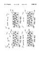
- FIG. 1An exemplary gyricon display 10 is shown in side view in FIG. 1 (PRIOR ART).
- Bichromal balls 1are disposed in an elastomer substrate 2 that is swelled by a dielectric fluid creating cavities 3 in which the balls 1 are free to rotate.
- the balls 1are electrically dipolar in the presence of the fluid and so are subject to rotation upon application of an electric field, as by matrix-addressable electrodes 4a, 4b.
- the electrode 4a closest to upper surface 5is preferably transparent.
- An observer at Isees an image formed by the black and white pattern of the balls 1 as rotated to expose their black or white faces (hemispheres) to the upper surface 5 of substrate 2.
- Gyricon displayshave numerous advantages over conventional electrically addressable visual displays, such as LCD and CRT displays.
- theyare suitable for viewing in ambient light, retain an image indefinitely in the absence of an applied electric field, and can be made lightweight, flexible, foldable, and with many other familiar and useful characteristics of ordinary writing paper.
- theyare suitable both for display applications and for so-called electric paper or interactive paper applications, in which they serve as an electrically addressable, reuseable (and thus environmentally friendly) substitute for ordinary paper.
- U.S. Pat. No. 5,389,945incorporated by reference hereinabove.
- gyricon displayspromise to offer many of the advantages of ordinary paper together with the advantages of electrically addressable displays
- the gyricon displays of the prior arthave not lived up to their promise. Simply put, these displays do not look as good as paper. In particular, they do not have the high reflectance of paper (typically, 85 percent diffuse reflectance for white paper) and, consequently, do not have the high brightness and contrast characteristics of paper.
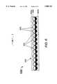
- FIG. 2The series of views of FIG. 2 (PRIOR ART) illustrates several different thick arrangements of bichromal balls found in various gyricon displays of the prior art.
- View (a)shows first arrangement 210, which is made up of bichromal balls 211 in spherical cavities 212 arrayed so as to form multiple layers 217, 218, 219.
- View (b)shows second arrangement 220, which is made up of bichromal balls 221 in spherical cavities 222 arrayed in wavy layers 227, 228, 229; as can be seen, the division of second arrangement 220 into layers 227, 228, 229 is somewhat arbitrary.
- View (c)shows third arrangement 230, which is made up of bichromal balls 231 in spherical cavities 232 that are not layered at all, but instead are distributed randomly throughout the thickness of arrangement 230.
- a thick displayhas certain drawbacks. Notably, a thinner display should require a lower drive voltage. Nevertheless, in keeping with the conventional wisdom, virtually all known gyricon displays are made with thick arrangements of bichromal balls (e.g., sheets of bichromal balls wherein the sheets are several ball diameters thick), because this is thought to be necessary in order to produce displays of adequate brightness.
- bichromal ballse.g., sheets of bichromal balls wherein the sheets are several ball diameters thick
- FIG. 6 and FIGS. 12-13 of the '160 patentare not to the contrary.
- the specification describing FIG. 6 and FIGS. 12-13 of the '160 patentmakes no mention whatsoever of the relative diameters of balls and cavities.
- the technique disclosed for forming the cavitiessuggests that the relative dimensions illustrated in FIG. 6 and in FIGS. 12-13 of the '160 patent are misleading, and that in practice, the cavities will be considerably larger than the balls.
- the '160 patentdoes not specify the particular method for deposition of wax on the balls (see '160 patent at col.
- the inventionprovides a gyricon display having superior reflectance characteristics comparing favorably with those of white paper.
- the inventiondefies the conventional wisdom that says "a thicker display is brighter," and instead proposes a gyricon display having a tightly packed monolayer of bichromal balls. Within this layer the balls are placed, preferably in a hexagonally packed array, so that adjacent ball surfaces are as close to one another as possible. The light reflected from the inventive gyricon display is reflected substantially entirely from the monolayer of balls, so that lower layers are not needed. By eliminating the lower layers, the display can be made thinner, which in turn provides further advantages, such as lower drive voltage and better resolution due to better control of fringing fields.
- the inventionprovides a material comprising a substrate having a surface and a plurality of optically anisotropic particles disposed in the substrate.
- the particles situated closest to the substrate surfaceform substantially a single layer.
- Each particle in the layerhas a center point, with substantially no particle in the layer being disposed entirely behind the center point of any nearest neighboring particle in the layer with respect to the substrate surface.
- Each particle in the layerhas a projected area with respect to the substrate surface, the particles of the set being sufficiently closely packed with respect to one another in the layer that the union of their projected areas exceeds two-thirds of the area of the substrate surface.
- a rotatable disposition of each particleis achievable while the particle is thus disposed in the substrate; for example, the particles can already be rotatable in the substrate, or can be rendered rotatable in the substrate by a nondestructive operation performed on the substrate.
- the substratecan be made up of an elastomer that is expanded by application of a fluid thereto so as to render the particles rotatable therein.
- a particle, when in its rotatable disposition,is not attached to the substrate.
- a display apparatuscan be constructed from a piece of the material together with means (such as an electrode assembly) for facilitating a rotation of at least one particle rotatably disposed in the substrate of the piece of material.
- the inventionprovides a material comprising a substrate having a surface and a plurality of optically anisotropic particles disposed in the substrate.
- Each particlehas an optically reflective component region.
- Each particlehas a preferred rotational orientation wherein the reflective region of the particle is proximate to the substrate surface.
- a rotatable disposition of each particleis achievable while the particle is thus disposed in the substrate.
- a particle, when in its rotatable disposition,is not attached to the substrate.
- Particlesare arranged in the substrate such that when a light susceptible to reflection by the reflective regions of the particles is incident on a portion of the substrate surface so as to illuminate therethrough those particles located in a vicinity thereof while those particles are rotationally oriented in their preferred orientations, the illuminated particles modulate the light that illuminates them such that at least 15 percent (and more preferably, at least 30 percent; and still more preferably, at least 40 percent; etc.) of the light incident on said portion of the surface is ultimately reflected (e.g., diffusely reflected) back through the substrate surface as measured by an integrating sphere technique.
- FIG. 1is an exemplary gyricon display of the PRIOR ART
- FIGS. 2(a)-2(c)are a series of views showing perfectly layered, imperfectly layered, and nonlayered (random) ball arrangements in gyricon displays of the PRIOR ART;
- FIGS. 3(a)-3(d)are a series of views exemplifying light scattering pathways for each of several individual gyricon balls according to the light rectifier model;
- FIGS. 4(a)-4(d)are a series of views exemplifying light scattering pathways in a gyricon display according to the light rectifier model
- FIGS. 5(a)-5(d)are a series of views contrasting exemplary light pathways in an ideal close-packed monolayer gyricon display, a high-quality close-packed monolayer gyricon display, a non-close-packed monolayer gyricon display, and a non-monolayer gyricon display with a close-packed top layer;
- FIG. 6illustrates a side view of a gyricon display of the present invention in an embodiment wherein the gyricon balls are arrayed in a close-packed monolayer;
- FIG. 7illustrates a side view of a gyricon display of the present invention in an alternative embodiment wherein the gyricon balls are arrayed in multiple layers with a close-packed monolayer as the layer closest to the viewing surface;
- FIG. 8illustrates a top view of a gyricon display of the present invention in an embodiment wherein the gyricon balls nearest the viewing surface are arrayed in a close-packed hexagonal formation;
- FIGS. 9 and 10illustrate top views of gyricon displays of the present invention in alternative embodiments wherein the gyricon balls are arrayed, respectively, in a close-packed rectangular formation and in a close-packed rhomboidal (diamond-shaped) formation;
- FIGS. 11(a)-11(f)are a series of views illustrating examples of gyricon displays each having two different populations of bichromal balls, with smaller-diameter bichromal balls filling the interstices in an ideal close-packed monolayer of larger-diameter bichromal balls;
- FIG. 12illustrates a side view of a gyricon display of the present invention in an embodiment wherein relatively large gyricon balls are arrayed in a close-packed formation, and relatively small gyricon balls fill the interstices of the formation;
- FIG. 13illustrates a top view of a gyricon display of the present invention in an embodiment wherein relatively large gyricon balls are arrayed in a close-packed hexagonal formation, and relatively small gyricon balls fill the interstices of the formation;
- FIGS. 14(a) and 14(b)a series of views contrasting the fringing fields in thick gyricon displays with the fringing fields in monolayer gyricon displays;
- FIG. 15is a photomicrograph of a thick gyricon display
- FIG. 16illustrates an example of the areal coverage fraction ⁇
- FIGS. 17(a) and 17(b)a series of views showing the relationships among center-to-center spacing, ball diameter, and cavity size;
- FIGS. 18-20illustrates the calculation of the areal coverage fraction ⁇ in, respectively, hexagonally, rectangularly, and rhomboidally (diamond) packed monolayer geometries of uniform bichromal spheres;
- FIG. 21illustrates an alternative embodiment of the invention in which a close-packed monolayer of gyricon balls is placed in a fluid directly between transparent electrodes, without an elastomer or other cavity-containing substrate medium.
- Bichromal ballshave a light side and a dark side.
- the research leading to the present inventioncan be thought of (with apologies to George Lucas) as an exploration of the dark side.
- This researchshows why the conventional wisdom that "thicker is brighter” fails, and offers in its place a new, more effective model of light propagation in a gyricon display, called the light rectifier model.
- the new modelmotivates the proposed close-packed monolayer gyricon display according to the invention.
- the bichromal balls used in a gyricon displayare white on one hemispherical surface and black on the other.
- the balls thereinare oriented so that their white hemispheres face up (that is, face toward the viewing surface of the display, so as to be visible to an observer located above the display as is the observer at I in FIG. 1).
- Light coming in from above the displayis diffusely scattered in many directions from the tops of the balls.
- FIG. 3illustrates these ideas.
- Each of the series of views (a), (b), (c), (d) in FIG. 3shows a portion of gyricon display 300 including bichromal balls 331, 332, 333, and 334, all of which are turned so that their white hemispheres face up towards transparent viewing surface 310.
- Light rays from a light source Lpass through viewing surface 310 to be scattered by the white hemispheres of the bichromal balls.
- light ray 325strikes a point at the very top of ball 331 and is scattered in all directions bounded by tangent plane T 1 . Almost all the scattered light can return through surface 310.
- ray 326strikes a point farther down ball 331 and is scattered in all directions bounded by tangent plane T 2 . Although most of the scattered light can return through surface 310, some of it is scattered downward and is absorbed by the black hemisphere of ball 332.
- ray 327strikes a point on ball 333 and is scattered in all directions bounded by tangent plane T 3 .
- the white hemisphere of ball 333is below the black hemispheres of other balls, such as ball 331.
- a substantial portion of the scattered lightis absorbed by the black hemispheres of ball 331 and other balls situated above ball 333 with respect to surface 310.
- ray 328strikes the top of ball 334 and is scattered in all directions bounded by tangent plane T 4 .
- Ball 334is below several other balls in the display, including balls 331, 332, and 333. Most of the light scattered from white hemisphere of ball 334 is absorbed by the black hermispheres of these other balls, and very little escapes through surface 310.
- a conventional gyricon display in the "white” stateacts as a light rectifier (analogous to an electrical rectifier).
- Light entering the devicecan pass downward easily, but cannot travel back upward without being absorbed. Put another way, once light goes in, in most cases it can't come out. Thus, any light that travels past the upper hemisphere of the topmost bichromal balls without being reflected is unlikely to escape the device. Adding bichromal balls below the topmost ones will contribute only minimally to overall display reflectance.
- FIG. 4illustrates various exemplary pathways for scattered light rays in gyricon displays according to the light rectifier model. (For clarity, only selected exemplary scattering pathways are shown; it will be understood that, as in FIG. 3, each light ray incident on the white hemisphere of a ball scatters at all angles bounded by the tangent plane at the point of incidence.)
- Each of the series of views (a), (b), (c), (d) in FIG. 4shows a portion of gyricon display 400, which is illuminated by light from diffuse illumination source L.
- the bichromal balls 407, 408, 409 in display 400are turned so that their white hemispheres are exposed to an observer at I. Balls 407 can be said to be the top or first layer of balls in display 400, balls 408 can be said to be the second layer, and balls 409 the third layer.
- light rays 451, 452, 453, 454, 461are incident on the topmost balls 407. No other balls lie between balls 407 and transparent viewing surface 410. Rays 451, 452, and 453 scatter immediately back to the observer at I. Ray 454 scatters from one ball and onto the white hemisphere of another ball, and thence back to the observer at I. Ray 461 strikes ball 437, a ball whose white hemisphere is somewhat lower than the black hemispheres of most of the other topmost balls 407. Ray 461 scatters off the white hemisphere of ball 437 and is absorbed by the black hermisphere of ball 438.
- topmost balls 407such as rays 451, 452, 453, and 454.
- rays 451, 452, 453, and 454are reflected so as to be visible to the observer at I; only a small portion of the rays incident on topmost balls 407 (for example, ray 461) are lost to absorption.
- Absorptive lossesare more substantial for balls (such as ball 437) that are situated below, rather than at the same depth as, the other balls in the top layer, and are particularly large for balls whose reflective white hemispheres lie below the absorptive black hemispheres of neighboring balls.
- light rays 462, 463, 464, 465, 455are incident on balls 408.
- Rays 462, 463, 464, and 465each scatter from the white hemisphere of one of the second-layer balls 408, but are then absorbed by the black hemispheres of topmost balls 407, and so do not escape to surface 410.
- these rays 462, 463, 464, 465are not visible to the observer at I.
- light rays 466, 467, 468, 469, 470are incident on balls 409. Some of these rays, such as rays 466 and 467, travel directly from light source L to balls 409 while others, such as rays 468, 469 and 470, arrive indirectly after being scattered from topmost balls 407 or second-layer balls 408, both of which lie between balls 409 and transparent viewing surface 410. Rays 466, 467, 468, 469, 470 each scatter from the white hemisphere of one of the third-layer balls 409, but are then absorbed by the black hemispheres of topmost balls 407 or second-layer balls 408, and so do not escape to surface 410.
- light rays 471, 472pass entirely through gyricon display 400 without encountering any of balls 407, 408, or 409. These rays pass through gaps between the balls and are not reflected (e.g., they are absorbed behind rear surface 420 of the display). Thus they are not visible to the observer at I.
- the light rectifier properties inherent in conventional gyricon displayscan be overcome by constructing a gyricon display in which all the bichromal balls are disposed in a single layer, at the same depth from the viewing surface, and packed as closely together as possible within that layer.
- a gyricon displayin which all the bichromal balls are disposed in a single layer, at the same depth from the viewing surface, and packed as closely together as possible within that layer.
- FIG. 5illustrates exemplary light scattering pathways in various gyricon displays.
- View (a)shows an ideal close-packed monolayer gyricon display 500 with bichromal balls 501.
- the surfaces of neighboring ballstouch each other, or come as close as possible to touching each other as is consistent with proper ball rotation.
- the only gaps between balls 501are the spaces that inherently arise when spheres are packed into a planar array.
- a hexagonal arrayis used.
- Display 500can be built by placing the balls 501 directly in the dielectric fluid without an elastomer, as will be described below with reference to FIG. 21.
- Rays 550, 551, 552, 553, and 554 from diffuse light source Lscatter from the upper white hemispheres of balls 501 and back out of display 500, thereby contributing to the observable brightness of the display.
- view (b)shows a high-quality (i.e., high-brightness) close-packed monolayer gyricon display 510, in which bichromal balls 511 rotate within cavities 512.
- Cavities 512can be formed, for example, by the swelled-elastomer techniques used in constructing conventional gyricon displays.
- Bichromal balls 511are preferably disposed in a planar hexagonal array, and cavities 512 are made as small as possible with respect to balls 511. Also, cavities 512 are placed as close to one another as possible, preferably with the walls between neighboring cavities being made as thin as possible and ideally approaching zero thickness. Thus the gaps between balls 511 are minimized.
- view (c)shows a monolayer gyricon display 520 of lesser quality, in which the bichromal balls are not as closely packed as in displays 500 and 510.
- Balls 521rotate within cavities 522; the spacing between adjacent cavities is relatively large with respect to the ball diameter. Therefore, more light is lost than in displays 500 and 510.
- Rays 560 and 562pass through the gaps between balls 521, and ray 563 is scattered so as to be absorbed by the black hemisphere of one of balls 521.
- the spacing between neighboring bichromal ballscan be large either because of large-sized cavities or, as shown in view (c), large spaces between adjacent cavities.
- Gyricon display 540has a thick arrangement of bichromal balls including top layer 547, middle layer 548, and bottom layer 549.
- the balls in top layer 547are close-packed in the same way as the balls 511 in the single layer of display 510 (from view (b)).
- the balls in layers 548 and 549are not close-packed.
- almost all the light observably reflected from display 540is reflected from the upper white hemisphere of balls in top layer 547, so layers 548 and 549 do not contribute substantially to the reflectance of display 540.
- the reflectance of display 540is about as good as that of display 510. Even so, for reasons discussed below with reference to FIG. 14, the thinner display 510 is to be preferred over the thicker display 540.
- a gyricon displayis built that does not act as a light rectifier.
- the inventive displayreflects entirely from the topmost layer of bichromal balls and, more particularly, from the white hemispherical upper surfaces of the topmost layer of balls.
- the inventive displayis constructed with a single close-packed monolayer of bichromal balls.
- FIGS. 3-5depict their respective gyricon displays in simplified form, so that the light pathways therein can be clearly seen.
- FIG. 6provides a more detailed side view of a gyricon display 600 of the invention in a specific embodiment.
- bichromal balls 601are placed as close to one another as possible in a monolayer in elastomer substrate 602.
- Substrate 602is swelled by a dielectric fluid (not shown) creating cavities 603 in which the balls 601 are free to rotate.
- the cavities 603are made as small as possible with respect to balls 601, so that the balls nearly fill the cavities.
- cavities 603are placed as close to one another as possible, so that the cavity walls are as thin as possible.
- balls 601are of uniform diameter and situated at a uniform distance from upper surface 605. It will be appreciated that the arrangement of balls 601 and cavities 603 in display 600 is comparable to that of balls 511 and cavities 512 in display 510 shown in view (b) of FIG. 5. It will further be appreciated that the arrangement of balls 601 and cavities 603 in display 600 minimizes both the center-to-center spacing and the surface-to-surface spacing between neighboring bichromal balls. (A more detailed discussion of the relative dimensions of the balls and the cavities within which they rotate will be provided below with reference to FIG. 17.)
- Balls 601are electrically dipolar in the presence of the dielectric fluid and so are subject to rotation upon application of an electric field, as by matrix-addressable electrodes 604a, 604b.
- the electrode 604a closest to upper surface 605is preferably transparent.
- An observer at Isees an image formed by the black and white pattern of the balls 601 as rotated to expose their black or white hemispheres to the upper surface 605 of substrate 602.
- FIG. 7shows a side view of a gyricon display 700 of the invention in an alternative embodiment.
- bichromal balls 701are in a top layer 707 and additional lower layers (here represented by second layer 708). Balls in top layer 707 are placed as close to one another as possible in a monolayer.
- Elastomer substrate 702is swelled by a dielectric fluid (not shown) creating cavities 703 in which the balls 701 are free to rotate. Cavities 703 are made as small as possible with respect to balls 701, and particularly with respect to balls in top layer 707, so that these balls nearly fill the cavities. Also, cavities 703 are placed as close to one another as possible, so that the cavity walls are as thin as possible.
- balls in top layer 707are of uniform diameter and are situated at a uniform distance from upper surface 705. It will be appreciated that the arrangement of balls and cavities in top layer 707 of display 700 is comparable to that of balls and cavities in top layer 547 in display 540 shown in view (d) of FIG. 5. It will further be appreciated that almost all the light reflected from display 700 so as to be observable to an observer at I is reflected from the white hemispheres of balls in top layer 707. At least for top layer 707, the arrangement of balls 701 and cavities 703 in display 700 minimizes both the center-to-center spacing and the surface-to-surface spacing between neighboring bichromal balls. Preferably, balls in the lower layers (such as layer 708) are also close-packed insofar as possible, in order to minimize display thickness.
- Balls 701are electrically dipolar in the presence of the dielectric fluid and so are subject to rotation upon application of an electric field, as by matrix-addressable electrodes 704a, 704b.
- the electrode 704a closest to upper surface 705is preferably transparent. An observer at I sees an image formed by the black and white pattern of the balls 701 as rotated to expose their black or white hemispheres to the upper surface 705 of substrate 702.
- monolayer display 600 of FIG. 6is preferable to the thicker display 700 of FIG. 7, for reasons discussed below with reference to FIG. 14.
- the lower layerssuch as layer 708, contribute little or nothing to observable display reflectance.
- the white hemispheres of balls in lower layer 708are situated so that any light that does reach them is most likely to be scattered into the absorptive dark sides of balls in top layer 707. Nevertheless, there can be situations where a display such as display 700 is preferred, for example, if such a display can be manufactured at less expense.
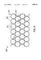
- FIG. 8illustrates this geometry.
- a top view of a portion of a gyricon display 800 of the inventionis shown, with the white hemispheres of the balls 801 visible through transparent viewing surface 805.
- Balls 801rotate in cavities 803, which cavities are preferably as small and close together as possible.
- the centers of balls 801form a hexagonal pattern as shown by exemplary hexagon H; that is, the centers of close neighboring balls form equilateral triangles, as shown by exemplary equilateral triangle E.
- Interstices 807occur as a result of the geometry (packed spheres cannot cover a plane entirely).
- FIGS. 9-10illustrate alternative packing geometries. These geometries are less preferred than the hexagonal geometry of FIG. 8, because they cover a smaller proportion of the plane than is covered by the hexagonal geometry.
- FIG. 9shows a rectangular geometry.
- a portion of gyricon display 900has bichromal balls 901 in cavities 903. The white hemispheres of balls 901 are visible through viewing surface 905.
- the rectangular geometryis shown by exemplary square S formed by the centers of balls 901. Interstices 907 are left unfilled by the packing geometry.
- FIG. 10shows a rhomboidal (diamond-shaped) geometry.
- a portion of gyricon display 1000has bichromal balls 1001 in cavities 1003. The white hemispheres of balls 1001 are visible through viewing surface 1005.
- the rhomboidal geometryis shown by exemplary rhombus R formed by the centers of balls 1001. Interstices 1007 are left unfilled by the packing geometry.
- interstices 807are formed by the hexagonal packing geometry.
- interstices 907are formed by the rectangular packing geometry.
- interstices 1007are formed by the rhomboidal packing geometry. According to the light rectifier model, light that passes through the interstices into the depths of the display is essentially lost.
- a gyricon displayis constructed from two populations of bichromal balls.
- balls in the first, or main, populationare of a first uniform diameter and balls in the second, or interstitial, population are of a second uniform diameter, with the second diameter chosen so that the balls in the second population can fill the interstices left by close-packing the balls from the first population.
- FIG. 11provides some examples of these ideas.
- Each of the series of views in FIG. 11illustrates a hexagonally packed planar array of bichromal balls 1101 with various smaller bichromal balls being used to fill the interstices of the array.
- the white hemispheres of balls 1101face upwards, and their topmost points lie in a plane P.
- Views (a) and (b)show, respectively, side and top views of the array of bichromal balls 1101. Smaller bichromal balls 1102 are situated above balls 1101 (that is, closer to the viewing surface of the gyricon display) in the interstices formed by the hexagonal packing arrangement. Balls 1102 also have their white hemispheres facing upwards.
- Balls 1102are of a diameter such that the plane that separates their white and black hemispheres is plane P. Views (c) and (d) show, respectively, side and top views of the array of bichromal balls 1101, with smaller bichromal balls 1102' situated above balls 1101 in the interstices formed by the hexagonal packing arrangement. Balls 1102' are of a diameter such that their topmost points lie in plane P. Views (e) and (f) show, respectively, side and top views of the array of bichromal balls 1101, with smaller bichromal balls 1102" situated above balls 1101 in the interstices formed by the hexagonal packing arrangement.
- Balls 1102"are hidden by balls 1101 and, accordingly, are shown as dashed outlines.
- Balls 1102"are of a diameter such that their surfaces are tangential to the surfaces of balls 1101 when their centers are coplanar with the centers of balls 1101, as shown.
- interstitial ballsare situated in a planar array above the planar array of the main bichromal balls. That is, the plane formed by the centers of the smaller balls is closer to the viewing surface than the plane formed by the centers of the monolayer (or close-packed top layer) of larger balls. With this arrangement, light reflected from the white hemispheres of the interstitial balls is not absorbed by the black hemispheres of the main bichromal balls, as would be the case if the interstitial balls were disposed below the layer of larger balls.
- the interstitial ballspreferably are small enough so that their black hemispheres do not absorb much of the light reflected by the white hemispheres of the main bichromal balls.
- a tradeoffcan be made between losses due to absorption by the black hemispheres of the interstitial balls and losses due to passage of light through unfilled portions of the interstices.
- balls 1102almost completely fill the interstices between balls 1101. However, some of the light scattered from the white hemispheres of balls 1101 is absorbed by the black hemispheres of balls 1102.
- balls 1102'being smaller than balls 1102 can be situated with their centers below plane P, so that light scattered by the white hemispheres of balls 1101 is less likely to reach the black hemispheres of balls 1102' than the black hemispheres of balls 1102.
- balls 1102"only partly fill the interstices between balls 1101.
- Balls 1102"are situated with their centers in the same plane as the centers of balls 1101, so very little of the light scattered from the white hemispheres of balls 1101 is absorbed by the black hemispheres of balls 1102".
- lightcan pass through the portions of the interstices between balls 1101 that are left unfilled by balls 1102". Therefore, with interstitial balls 1102", more light is transmitted beyond the white hemispheres of balls 1101 than is the case with the larger interstitial balls 1102 or 1102'.
- interstitial ballscan be situated lower with respect to the tops of the main bichromal balls, and so can be made to absorb less light with their black hemispheres.
- the interstitial ballsfill a smaller part of the interstitial gaps between the main bichromal balls, and so allow more light to pass beyond one hemisphere's depth in the main layer, thereafter to be lost to absorption.
- FIG. 12provides a more detailed side view of a gyricon display 1200 of the invention in a specific embodiment with main and interstitial bichromal balls.
- main bichromal balls 1201are placed as close to one another as possible in a monolayer in elastomer substrate 1202.
- Substrate 1202is swelled by a dielectric fluid (not shown) creating cavities 1203 in which the balls 1201 are free to rotate.
- the cavities 1203are made as small as possible with respect to balls 1201, so that the balls nearly fill the cavities.
- cavities 1203are placed as close to one another as possible, so that the cavity walls are as thin as possible.
- balls 1201are of uniform diameter and situated at a uniform distance from upper surface 1205.
- the arrangement of balls 1201 and cavities 1203 in display 1200is comparable to that of balls 601 and cavities 603 in display 600 shown in FIG. 6.
- display 1200differs from display 600 by the addition of small interstitial balls 1215, which rotate in their own cavities 1216 created by swelling of elastomer substrate 1202 in the presence of the dielectric fluid.
- Balls 1215rotate together with balls 1201 upon application of an electric field, so that when the white hemispheres of balls 1201 are presented to an observer at I, the white hemispheres of balls 1215 are also presented, and similarly for the black hemispheres.
- balls 1215are of uniform diameter and are situated at a uniform distance from upper surface 1205, with the plane P 2 containing the centers of balls 1215 being closer to surface 1205 than the plane P 1 containing the centers of balls 1201.
- the distance z between the plane P 2 containing the centers of balls 1215 and the plane P 1 containing the centers of balls 1201is preferably minimized, so that balls 1215 are as close to balls 1201 as possible, thus minimizing absorptive losses due to light scattering from the white hemispheres of balls 1201 into the black hemispheres of balls 1215.
- Cavities 1216are made as small as possible with respect to balls 1215, so that the balls nearly fill the cavities, and the walls of cavities 1216 are made as thin as possible.
- FIG. 13shows a top view of a portion of display 1200.
- the white hemispheres of main bichromal balls 1201 and interstitial bichromal balls 1215can be seen through transparent surface 1205.
- a hexagonal packing geometryis used for balls 1201, as indicated by hexagon H and equilateral triangle E.
- Interstitial balls 1215fill the interstices 1217 left between balls 1201 in the hexagonal packing geometry.
- balls 1215can fill a greater or lesser portion of the interstices 1217, depending on the relative diameters of balls 1201 and balls 1215.
- the main bichromal ballscan be packed in rectangular or rhomboidal geometries, and can be either a monolayer of balls or the close-packed top layer of a thick arrangement of balls.
- the basic ideais to intercept incoming light that would otherwise be lost in the interstices and reflect it to the observer, either directly or by scattering from nearby white hemispheres of larger balls, while preferably minimizing absorptive losses due to the black hemispheres of the smaller balls.
- a monolayer gyricon display according to the inventionhas advantages in addition to improved reflectance.
- a lower operating voltagehas many advantages, including lower power consumption, less expensive drive electronics, and increased user safety.
- interstial balls to the displayneed not result in increased operating voltage over what is required for the monolayer display.
- the drive voltage for interstitially packed display 1200 of FIG. 12can be the same or comparable to the voltage used to drive monolayer display 600 of FIG. 6.
- the minimum electric field strength that must be applied to cause rotation of the smaller ballsis no greater than the minimum field strength for the larger balls. Therefore, so long as the addition of the smaller balls to the display does not increase the overall substrate thickness, the voltage need not be increased.
- the interstitial arrangements shown in views (c) and (e) of FIG. 11can be situated in substrates no thicker than the substrate needed for a simple monolayer of balls 1101. If the addition of the smaller balls does increase thickness over the monolayer thickness, as for the interstitial arrangement shown in view (a) of FIG. 11, a corresponding increase in voltage is required.
- addressing electrodes 1410 and 1411are used to address adjacent pixels in a bichromal gyricon display. Electrode 1410 is held at a positive voltage V+ and electrode 1411 is held at a negative voltage V- with respect to a ground plane 1420. Because the applied voltages are of opposite signs, the pixels addressed by electrodes 1410 and 1411 are of opposite colors. For example, if the pixel addressed by electrode 1410 appears white, then the pixel addressed by electrode 1411 appears black.
- the bichromal ballsare located in the space between addressing electrodes 1410, 1411 and ground plane 1420 (for clarity, only an exemplary few are shown in FIG. 14.)
- the distance h between electrodes 1410, 1411 and ground plane 1420is relatively large. This provides a relatively large volume in which fringing fields F can develop. These are fields whose field lines curve directly from electrode 1410 to electrode 1411 instead of running to ground plane 1420.
- Bichromal balls 1401 and 1402align in the preferred manner, with the white hemisphere of ball 1401 facing squarely towards electrode 1410 and the black hemisphere of ball 1402 facing squarely towards electrode 1411.
- bichromal balls 1403 and 1404are caught in the path of fringing fields F. These balls turn at an angle to electrodes 1410 and 1411. The result is that in the region of the fringing fields F, the display appears gray instead of black or white.
- the width w of the fringing fields (and thus of the gray region) in view (a)is comparable to the distance h between the electrodes 1410, 1411 and ground plane 1420.
- the distance h' between electrodes 1410, 1411 and ground plane 1420is relatively small, as for a monolayer display of the invention.
- Thisprovides a relatively small volume for fringing fields F' to develop.
- Bichromal balls 1401 and 1402align in the preferred manner, with the white hemisphere of ball 1401 facing squarely towards electrode 1410 and the black hemisphere of ball 1402 facing squarely towards electrode 1411.
- the volume of fringing fields F'is sufficiently small that very few balls are caught in the path of these fields. The result is a sharp demarcation between the black and white pixels, with very little of the gray intermediate region that was present in view (a).
- the width w' of the fringing fields (and thus of the gray region) in view (b)is comparable to the separation distance A between electrodes 1410 and 1411.
- the close-packed monolayer gyricon displaycan be fabricated by creating a monolayer of balls according to known techniques, such as that disclosed in "A Simple Method for the Production of a Two-Dimensional, Ordered Array of Small Latex Particles" by R. Micheletto, H. Fukuda, and M. Ohtsu, Langmuir, vol. 11, no. 9, 1995, pp. 3333-3336; preparing an elastomer sheet to contain the balls; and swelling the elastomer by application of a dielectric fluid.
- Preparation of the elastomercan be carried out as for the fabrication of a conventional gyricon display, except for the way in which the elastomer is cured.
- the elastomerswells over 50 percent upon application of the dielectric fluid, and the cavities in which the balls rotate are correspondingly large.
- the cavitiesshould be made considerably smaller. This can be accomplished, for example, by using Dow-Corning SYLGARD 184 elastomer and curing it with a 15-percent curing agent (hardener) at 90 degrees Celsius.
- the elastomerUpon application of ISOPAR L dielectric fluid, commonly used for known gyricon displays, the elastomer expands about 20 percent.
- alternative dielectric fluidscan be used in place of ISOPAR L. For example, for the above elastomer (15 percent cure at 90° C.), a dielectric fluid mixture of 50 percent ISOPAR L and 50 percent soybean oil yields about 10 percent expansion.
- a monolayer of the larger (main) bichromal ballsis prepared as described above. This monolayer is placed on a layer of sticky, partially cured elastomer.
- the sticky elastomer layeris of a depth such that its top surface is coplanar with, or slightly below, the plane in which the centers of the smaller (interstitial) balls are to lie. For example, if the display structure is as shown in view (e) of FIG. 11, the sticky elastomer layer will rise to a depth about halfway up the larger balls. If the display structure is as shown in view (a) of FIG.
- the sticky layerwill reach the tops of the larger balls, or just below them.
- the smaller (interstitial) ballsare dispersed over the monolayer.
- the smaller ballsstick to the elastomer exposed by the interstitial gaps between the larger balls.
- all the gapsare filled by small balls. This can be accomplished by dispersing more smaller balls than are needed to fill the gaps, and allowing excess smaller balls to pile on top of the balls stuck in the gaps.
- the sticky elastomeris not deep enough to reach the excess piled-up balls, so the excess balls can be shaken off, leaving only the stuck interstitial balls.
- Additional elastomercan then be added, preferably while the sticky layer is still sticky (that is, prior to full curing), as by pouring uncured liquid elastomer over the entire assemblage to sufficient depth as to cover the tops of the main and interstitial balls. In this way, the elastomer substrate can be built up to a desired thickness.
- Gyricon displayscontain a large number of small particles. According to conventional wisdom, in the white state, these particles should diffusely reflect incoming light back out of the display. This desired result is similar to the reflection process in ordinary white paper and in other optical systems, such as white paint, white clouds, or milk. In other words, it is conventionally supposed that standard reflection theories, such as Kubelka-Munk theory, should apply to gyricon displays.
- FIG. 15A photomicrograph of a thick gyricon display, taken during the course of the research, is shown in FIG. 15. As can be seen, only the balls located close to the top surface of the gyricon display appear to be white. Balls located some distance from the surface appear increasingly dark as the depth increases. (This contrasts with what is observed in conventional diffuse scattering systems, such as paper or milk. In those systems, the particles below the surface still appear white.) Adding more balls to make a thicker gyricon display does not significantly increase reflectance, because the additional balls are located farther from the viewing surface and so appear dark, looking gray rather than white.
- bichromal ballsare dispersed throughout the thickness of the substrate sheet, which is always thicker than two ball diameters and is usually many diameters thick. Generally, less than 20 percent of the upper surface area of the sheet is covered by the bichromal balls in the layer closest to the surface. This corresponds to a spacing between ball centers on the order of twice the diameter of the balls. In other words, the gaps between adjacent bichromal balls of the topmost layer are quite large, and fewer than 20 percent of the balls are situated where they can contribute effectively to display reflectance.
- Ris the reflectance--more specifically, the diffuse reflectance--of the gyricon display, as measured by an integrating sphere technique. Integrating sphere measurement techniques are well known and are described, for example, in chapter 10 of Reflectance Spectroscopy by Wesley Wm. Wendlandt and Harry G. Hecht (Interscience Publishers, 1966); diffuse reflectance (as distinct from, for example, specular or total reflectance) is defined in chapter 3 of the same reference.
- the diffuse reflectance of high-quality white paperis typically 85 percent and that of newsprint is typically 60 percent.
- the inventive gyricon displayscan be expected to provide greatly improved diffuse reflectance, e.g., 30 percent, 40 percent, 60 percent, or even 80 or 85 percent, as opposed to gyricon displays of the prior art, for which the diffuse reflectance is at most 15 to 20 percent.
- the areal coverage fraction ⁇is defined as the ratio of the projected area of the white faces of the topmost bichromal balls of the gyricon display to the total area of the gyricon display viewing surface when all bichromal balls are turned with their white faces towards the viewing surface.
- adepends on geometry and can be computed either globally for an entire gyricon display or locally for any region thereof.
- Kis a parameter, treated here as a constant, that accounts for all sources of light loss other than the absorptive losses predicted by the light rectifier model.
- sources of light losscan include, for example, stray black spots or streaks in the white ball hemispheres, ball surface roughness or other surface defects, balls that fail to rotate completely, mismatches between the refractive indices of the elastomer or other substrate and the working fluid in which the balls rotate, etc. Equation (1) assumes that all these other sources of light loss can be treated as independent of light rectifier losses; this assumption is valid at least as a first-order approximation.
- FIG. 16An exemplary computation of ⁇ is illustrated schematically in FIG. 16.
- a selected portion of gyricon display 1600is shown.
- Bichromal balls of the displayare turned with their white hemispheres towards viewing surface 1605.
- Topmost bichromal balls 1607are those located closest to surface 1605; no other bichromal balls are situated between balls 1607 and surface 1605 where they could potentially absorb light reflected by balls 1607.
- Bichromal balls 1608are farther below surface 1605, so that topmost bichromal balls 1607 are between bichromal balls 1608 and surface 1605; thus the black hemispheres of topmost bichromal balls 1607 absorb most of the light reflected from bichromal balls 1608.
- balls 1607c and 1607dare separated by a distance whose projection in the plane of surface 1605 is ⁇ 34 and that the separation between balls 1607a and 1607b, and that between balls 1607b and 1607c, is also ⁇ 34 .
- the area Ais approximately twice the area of a square of width 2 ⁇ 34 , that is, approximately 8 ⁇ 34 2 . Therefore, ⁇ is computed to be the ratio ⁇ ( ⁇ 1 2 + ⁇ 2 2 + ⁇ 3 2 + ⁇ 4 2 )/8 ⁇ 34 2 .
- the other bichromal balls 1608do not contribute to the projected areas 1610, and thus do not figure in the calculation of ⁇ .
- ⁇depends on the size of the white hemisphere of each individual ball among the topmost bichromal balls and on the amount of empty space present between the topmost bichromal balls.
- ⁇is a measure of the average size of the bichromal balls.
- ⁇can be the maximum or mean diameter or radius of a spheroidal ball.
- ⁇is a measure of the average distance between ball centers, projected in the plane of the viewing surface.
- equation (2)For perfectly spherical balls of constant diameter d in a uniformly spaced monolayer array with characteristic spacing D, equation (2) reduces to the following equation (3): ##EQU1##
- xis the ratio (D-d)/d, where d is the diameter of each bichromal ball and D is the characteristic center-to-center spacing between adjacent balls. Note that if the cavities in which the balls rotate are of constant diameter and are close-packed so that the walls of adjacent cavities touch one another, D is equal to the diameter of the cavities.
- ⁇ ois the maximum theoretically possible areal coverage fraction for the particular packing geometry of the array; that is, ⁇ o is the areal coverage fraction obtained for a monolayer of spherical balls arranged in an ideal close-packed lattice of the selected geometry with surfaces of adjacent balls touching one another.
- ⁇ ocan be computed geometrically as described below with reference to FIGS. 18-20.
- ⁇ ois ⁇ divided by twice the square root of 3, that is, ⁇ /(2 ⁇ 3 1/2 ) or approximately 0.907; put another way, a planar close-packed hexagonal array of spheres covers approximately 0.907 times the total area of the plane. Therefore, for an ideal close-packed hexagonal monolayer array of bichromal balls and a planar viewing surface, the projected area of the ball hemispheres facing the viewing surface covers just under 91 percent of the total area of the viewing surface.
- FIG. 17illustrates the relationships among the quantities D and d of equation (3).
- Each of the series of views of FIG. 17shows a portion of a gyricon display that includes bichromal balls 1701 situated in cavities 1703 beneath viewing surface 1705.
- the diameter of balls 1701is d and the diameter of cavities 1703 is C.
- Dthe center-to-center spacing between balls 1701 is greater than C, and cavities 1703 are separated from one another by a distance of (D-C).
- D'the center-to-center spacing between balls 1701 is equal to C. Cavities 1703 touch one another as shown.
- FIG. 17elucidates an important interpretation of equation (3).
- xcan be interpreted as the expansion fraction, which is the fractional increase in elastomer size (linear dimension) that takes place when dielectric fluid is applied to expand the elastomer. Accordingly, when the conditions illustrated in view (b) of FIG. 17 obtain, equation (3) can be used to estimate how display reflectance (and thus display brightness) varies with varying degrees of elastomer expansion.
- xincreases as the center-to-center distance D increases, that is, as the packing density of the balls decreases.
- xincreases as the degree of elastomer expansion increases.
- Table 1lists values of R computed from equation (3) for various values of x and K. A hexagonal packing geometry is assumed.
- the reflectance Rdecreases rapidly as x increases.
- x0 and the projected area of the monolayer covers just under 91 percent of the viewing surface.
- Still greater areal coverage and reflectancecan be achieved by situating smaller balls within the interstices of the hexagonal packing arrangement, as was described above with reference to FIGS. 11-13.
- FIGS. 18-20illustrate the computation of the areal coverage fraction ⁇ and maximum areal coverage fraction ⁇ o for planar monolayers of uniform diameter spherical balls in various packing geometries.
- a hexagonal array of balls 1801 situated in cavities 1803is shown in a top view.
- Balls 1801have diameter d and center-to-center spacing D (equal to the cavity diameter, since cavities 1803 touch one another).
- the centers of neighboring ballsform an equilateral triangle E.
- the areal coverage fractionis computed as the ratio between the area of that portion of the triangle E overlapped by projected areas of balls 1801 and the area of the entire triangle E.
- the projected area for each of balls 1801is ⁇ d 2 /4.
- Three ballsare in the vicinity of triangle E.
- Triangle Ehas a base of length D.
- a rectangular array of balls 1901 situated in cavities 1903is shown in a top view.
- Balls 1901have diameter d and center-to-center spacing D.
- the centers of neighboring ballsform a square S.
- the areal coverage fractionis computed as the ratio between the area of that portion of the square S overlapped by projected areas of balls 1901 and the area of the entire square S.
- the projected area for each of balls 1901is ⁇ d 2 /4.
- Four ballsare in the vicinity of square S.
- Square Shas a base of length D.
- a rhomboidal array of balls 2001 situated in cavities 2003is shown in a top view.
- Balls 2001have diameter d and center-to-center spacing D.
- the centers of neighboring ballsform a rhombus R.
- each bichromal ballis situated in a cavity.
- the cavitiesare preferably made as small and as close together as possible.
- a gyricon displaycan be constructed without elastomer and without cavities.
- the bichromal ballsare placed directly in the dielectric fluid.
- the balls and the dielectric fluidare then sandwiched between two retaining members (e.g., between the addressing electrodes). There is no elastomer substrate.
- FIG. 21illustrates a side view of a no-cavities gyricon display.
- a monolayer of bichromal balls 2101 of uniform diameteris situated in dielectric fluid 2109 between matrix-addressable electrodes 2104a, 2104b.
- balls 2101are arranged in a hexagonal array within the monolayer, packed as close together as is possible consistent with proper ball rotation.
- Balls 2101are electrically dipolar in the presence of dielectric fluid 2109 and so are subject to rotation upon application of an electric field, as by electrodes 2104a, 2104b.
- the electrode 2104a closest to upper surface 2105is preferably transparent. An observer at I sees an image formed by the black and white pattern of the balls 2101 as rotated to expose their black or white hemispheres to the upper surface 2105 of display 2100.
- Electrodes 2104a, 2104bserve both to address balls 2101 and to retain balls 2101 and fluid 2109 in place.
- the spacing between electrodes 2104a, 2104bis as close to the diameter of balls 2101 as is possible consistent with proper ball rotation.
- Balls 2101 and fluid 2109can be sealed in display 2100, for example by seals at either end of the display (not shown).
- display 2100provides maximum reflectance and maximum brightness.
- Interstitial ballscan also be included in display 2100, for example by using the arrangement and interstitial ball diameter shown in views (c) and (d) of FIG. 11. The smaller balls are retained in place from above by upper electrode 2104a and from below by the larger balls 2101.
- Gyricon displayshave unique optical properties. Conventional approaches used to increase the reflectance of diffuse scattering arrays do not work well for gyricon displays. Conventional optical models, which assume that the bichromal balls situated well below the viewing surface of a gyricon display contribute as much to overall display brightness as do the bichromal balls nearest the viewing surface, do not accurately describe gyricon display optics. The light rectifier model provides a better description.
- the inventionprovides a new gyricon display based on a close-packed monolayer of bichromal balls.
- the design of the new displaytakes the light rectifier model into account, in that the light reflected from the display is reflected almost entirely from the upper hemispheres of balls in the close-packed monolayer.
- the inventive displayprovides superior reflectance and brightness characteristics as compared with conventional gyricon displays, and accordingly it provides superior contrast characteristics as well.
- the new displayrequires lower voltage than conventional gyricon displays, and can provide superior resolution inasmuch as electric field fringing effects are minimized. It is hoped that the new gyricon display of the invention will go a long way toward making the promise of electric paper come true.
- the electrical anisotropy of a gyricon ballneed not be based on zeta potential. It is sufficient that there is an electrical dipole moment associated with the ball, the dipole moment being aligned with respect to the ball in such a way as to facilitate a useful rotation of the ball in the presence of an applied external electric field. (Typically, the dipole moment is oriented along an axis of symmetry of the ball.) Further, it should be noted that a gyricon ball can have an electrical monopole moment in addition to its electrical dipole moment, as for example when the dipole moment arises from a separation of two positive charges of different magnitudes, the resulting charge distribution being equivalent to a positive electrical monopole superposed with a electrical dipole.
- the optical anisotropy of a gyricon ballneed not be based on black and white.
- bichromal balls having hemispheres of two different colors, e.g. red and bluecan be used.
- balls that are black in one hemisphere and mirrored in the othermight be used for some applications.
- various optical propertiescan vary as different aspects of a gyricon ball are presented to an observer, including (but not limited to) light scattering and light reflection in one or more regions of the spectrum.
- the gyricon ballscan be used to modulate light in a wide variety of ways.
- the incident light that encounters a gyricon displayneed not be restricted to visible light.
- the incident "light”can be, for example, infrared light or ultraviolet light, and such light can be modulated by the gyricon display.
- a gyricon display(or a sheet of bichromal balls for use in such a display) made of a flexible material can be temporarily or permanently deformed (for example, flexed, folded, or rolled) so as not to be strictly planar overall.
- the plane of a monolayercan be defined, for example, in a locally planar neighborhood that includes the gyricon ball or balls of interest.
- the monolayercan vary somewhat from what has been described, for example, due to manufacturing tolerances or slight imperfections of particular gyricon sheets.
- the inventive displaycan also be built using cylindrical elements in place of the usual spherical elements (e.g., bichromal cylinders instead of bichromal balls), as disclosed in copending, coassigned application 08/716,672, entitled “Twisting-Cylinder Display.”
- spherical elementse.g., bichromal cylinders instead of bichromal balls
Landscapes
- Physics & Mathematics (AREA)
- General Physics & Mathematics (AREA)
- Engineering & Computer Science (AREA)
- Theoretical Computer Science (AREA)
- Health & Medical Sciences (AREA)
- Life Sciences & Earth Sciences (AREA)
- Molecular Biology (AREA)
- Optics & Photonics (AREA)
- Electrochromic Elements, Electrophoresis, Or Variable Reflection Or Absorption Elements (AREA)
Abstract
Description
R=Kα (Eq. 1)
R=Kα(δ, Δ) (Eq. 2)
TABLE 1 ______________________________________ x R (K = 1.0) R (K = .7) R (K = .5) ______________________________________ 0.000 0.907 0.635 0.454 0.050 0.823 0.576 0.411 0.100 0.750 0.525 0.375 0.150 0.686 0.480 0.343 0.200 0.630 0.441 0.315 0.250 0.580 0.406 0.290 0.300 0.537 0.376 0.268 0.350 0.498 0.348 0.249 0.400 0.463 0.324 0.231 0.450 0.431 0.302 0.216 0.500 0.403 0.282 0.202 0.600 0.354 0.248 0.177 0.700 0.314 0.220 0.157 0.800 0.280 0.196 0.140 0.900 0.251 0.176 0.126 1.000 0.227 0.159 0.113 ______________________________________
Claims (27)
Priority Applications (10)
| Application Number | Priority Date | Filing Date | Title |
|---|---|---|---|
| US08/713,936US5808783A (en) | 1996-06-27 | 1996-09-13 | High reflectance gyricon display |
| BR9702315-9ABR9702315A (en) | 1996-06-27 | 1997-06-25 | Material and apparatus |
| JP50311998AJP4018149B2 (en) | 1996-06-27 | 1997-06-25 | Twisting ball display |
| PCT/US1997/010124WO1997050072A2 (en) | 1996-06-27 | 1997-06-25 | Twisting ball display |
| CNB971907897ACN1179311C (en) | 1996-06-27 | 1997-06-25 | Twisting-ball display |
| CA002229774ACA2229774C (en) | 1996-06-27 | 1997-06-25 | Twisting ball display |
| MX9801552AMX9801552A (en) | 1996-06-27 | 1997-06-25 | Twisting ball display. |
| DE69712030TDE69712030T2 (en) | 1996-06-27 | 1997-06-25 | ROTARY BALL DISPLAY |
| AU33876/97AAU3387697A (en) | 1996-06-27 | 1997-06-25 | Twisting ball display |
| EP97929929AEP0862773B1 (en) | 1996-06-27 | 1997-06-25 | Twisting ball display |
Applications Claiming Priority (2)
| Application Number | Priority Date | Filing Date | Title |
|---|---|---|---|
| US2052296P | 1996-06-27 | 1996-06-27 | |
| US08/713,936US5808783A (en) | 1996-06-27 | 1996-09-13 | High reflectance gyricon display |
Publications (1)
| Publication Number | Publication Date |
|---|---|
| US5808783Atrue US5808783A (en) | 1998-09-15 |
Family
ID=26693552
Family Applications (1)
| Application Number | Title | Priority Date | Filing Date |
|---|---|---|---|
| US08/713,936Expired - LifetimeUS5808783A (en) | 1996-06-27 | 1996-09-13 | High reflectance gyricon display |
Country Status (1)
| Country | Link |
|---|---|
| US (1) | US5808783A (en) |
Cited By (325)
| Publication number | Priority date | Publication date | Assignee | Title |
|---|---|---|---|---|
| US6067185A (en) | 1997-08-28 | 2000-05-23 | E Ink Corporation | Process for creating an encapsulated electrophoretic display |
| US6120839A (en) | 1995-07-20 | 2000-09-19 | E Ink Corporation | Electro-osmotic displays and materials for making the same |
| US6122094A (en)* | 1998-10-16 | 2000-09-19 | Xerox Corporation | Additive color electric paper without registration or alignment of individual elements |
| US6249271B1 (en) | 1995-07-20 | 2001-06-19 | E Ink Corporation | Retroreflective electrophoretic displays and materials for making the same |
| US6262833B1 (en) | 1998-10-07 | 2001-07-17 | E Ink Corporation | Capsules for electrophoretic displays and methods for making the same |
| US6262706B1 (en) | 1995-07-20 | 2001-07-17 | E Ink Corporation | Retroreflective electrophoretic displays and materials for making the same |
| US6300932B1 (en) | 1997-08-28 | 2001-10-09 | E Ink Corporation | Electrophoretic displays with luminescent particles and materials for making the same |
| US20020021270A1 (en)* | 2000-08-17 | 2002-02-21 | Albert Jonathan D. | Bistable electro-optic desplay, and method for addressing same |
| US6376828B1 (en) | 1998-10-07 | 2002-04-23 | E Ink Corporation | Illumination system for nonemissive electronic displays |
| US6377387B1 (en) | 1999-04-06 | 2002-04-23 | E Ink Corporation | Methods for producing droplets for use in capsule-based electrophoretic displays |
| US6383619B1 (en) | 1998-01-30 | 2002-05-07 | 3M Innovative Properties Company | Reflective particle display film and method of manufacture |
| US20020063661A1 (en)* | 2000-11-29 | 2002-05-30 | E Ink Corporation | Addressing schemes for electronic displays |
| US20020090980A1 (en)* | 2000-12-05 | 2002-07-11 | Wilcox Russell J. | Displays for portable electronic apparatus |
| US6440252B1 (en) | 1999-12-17 | 2002-08-27 | Xerox Corporation | Method for rotatable element assembly |
| US6445489B1 (en) | 1998-03-18 | 2002-09-03 | E Ink Corporation | Electrophoretic displays and systems for addressing such displays |
| US20020130832A1 (en)* | 2001-03-13 | 2002-09-19 | Baucom Allan Scott | Apparatus for displaying drawings |
| US6462859B1 (en) | 2000-10-04 | 2002-10-08 | 3M Innovative Properties Company | Electromagnetically responsive particle assembly and methods and articles for manufacture and use |
| US6473072B1 (en) | 1998-05-12 | 2002-10-29 | E Ink Corporation | Microencapsulated electrophoretic electrostatically-addressed media for drawing device applications |
| US6486861B1 (en) | 1999-05-07 | 2002-11-26 | Xerox Corporation | Method and apparatus for a display producing a fixed set of images |
| US6486866B1 (en)* | 1998-11-04 | 2002-11-26 | Sony Corporation | Display device and method of driving the same |
| US20020190936A1 (en)* | 1999-09-28 | 2002-12-19 | Brother International Corporation | Methods and apparatus for subjecting an element to an electrical filed |
| US6498114B1 (en) | 1999-04-09 | 2002-12-24 | E Ink Corporation | Method for forming a patterned semiconductor film |
| US6498674B1 (en) | 2000-04-14 | 2002-12-24 | Xerox Corporation | Rotating element sheet material with generalized containment structure |
| US6504525B1 (en) | 2000-05-03 | 2003-01-07 | Xerox Corporation | Rotating element sheet material with microstructured substrate and method of use |
| US20030011560A1 (en)* | 1998-08-27 | 2003-01-16 | E Ink Corporation | Electrophoretic display comprising optical biasing element |
| US20030011867A1 (en)* | 2001-07-09 | 2003-01-16 | Loxley Andrew L. | Electro-optic display and adhesive composition for use therein |
| US6515649B1 (en) | 1995-07-20 | 2003-02-04 | E Ink Corporation | Suspended particle displays and materials for making the same |
| US20030025855A1 (en)* | 2001-07-09 | 2003-02-06 | E Lnk Corporation | Electro-optic display and lamination adhesive |
| US6518949B2 (en) | 1998-04-10 | 2003-02-11 | E Ink Corporation | Electronic displays using organic-based field effect transistors |
| US20030053189A1 (en)* | 2001-09-14 | 2003-03-20 | E Ink Corporation | Methods for addressing electro-optic materials |
| US6545671B1 (en) | 2000-03-02 | 2003-04-08 | Xerox Corporation | Rotating element sheet material with reversible highlighting |
| US6549327B2 (en) | 2001-05-24 | 2003-04-15 | Xerox Corporation | Photochromic gyricon display |
| US20030132924A1 (en)* | 2002-01-16 | 2003-07-17 | Hamilton Robert S. | E-paper labels on recordable/removable media with optical data link and optical power supply |
| US20030137521A1 (en)* | 1999-04-30 | 2003-07-24 | E Ink Corporation | Methods for driving bistable electro-optic displays, and apparatus for use therein |
| US6621766B2 (en) | 2001-08-01 | 2003-09-16 | Fossil, Inc. | Flexible timepiece in multiple environments |
| US20030214695A1 (en)* | 2002-03-18 | 2003-11-20 | E Ink Corporation | Electro-optic displays, and methods for driving same |
| US20030222315A1 (en)* | 2002-04-24 | 2003-12-04 | E Ink Corporation | Backplanes for display applications, and components for use therein |
| US6661563B2 (en)* | 2000-01-31 | 2003-12-09 | Fujitsu Limited | Sheet-shaped display, sphere-like resin body, and micro-capsule |
| WO2003107315A2 (en) | 2002-06-13 | 2003-12-24 | E Ink Corporation | Methods for driving electro-optic displays |
| USD485294S1 (en) | 1998-07-22 | 2004-01-13 | E Ink Corporation | Electrode structure for an electronic display |
| US20040008398A1 (en)* | 2002-06-27 | 2004-01-15 | E Ink Corporation | Illumination system for nonemissive electronic displays |
| US20040014265A1 (en)* | 2002-04-24 | 2004-01-22 | E Ink Corporation | Processes for forming backplanes for electro-optic displays |
| US20040012839A1 (en)* | 2002-05-23 | 2004-01-22 | E Ink Corporation | Capsules, materials for use therein and electrophoretic media and displays containing such capsules |
| US20040021964A1 (en)* | 2002-02-19 | 2004-02-05 | Mario Rabinowitz | Mini-optics solar energy concentrator |
| US6690350B2 (en) | 2001-01-11 | 2004-02-10 | Xerox Corporation | Rotating element sheet material with dual vector field addressing |
| US20040027327A1 (en)* | 2002-06-10 | 2004-02-12 | E Ink Corporation | Components and methods for use in electro-optic displays |
| US6693620B1 (en) | 1999-05-03 | 2004-02-17 | E Ink Corporation | Threshold addressing of electrophoretic displays |
| US6704133B2 (en) | 1998-03-18 | 2004-03-09 | E-Ink Corporation | Electro-optic display overlays and systems for addressing such displays |
| US6727881B1 (en) | 1995-07-20 | 2004-04-27 | E Ink Corporation | Encapsulated electrophoretic displays and methods and materials for making the same |
| US20040105036A1 (en)* | 2002-08-06 | 2004-06-03 | E Ink Corporation | Protection of electro-optic displays against thermal effects |
| US20040112750A1 (en)* | 2002-09-03 | 2004-06-17 | E Ink Corporation | Electrophoretic medium with gaseous suspending fluid |
| US20040136048A1 (en)* | 1995-07-20 | 2004-07-15 | E Ink Corporation | Dielectrophoretic displays |
| US20040155857A1 (en)* | 2002-09-03 | 2004-08-12 | E Ink Corporation | Electro-optic displays |
| US20040196215A1 (en)* | 2002-12-16 | 2004-10-07 | E Ink Corporation | Backplanes for electro-optic displays |
| US20040226820A1 (en)* | 2003-03-25 | 2004-11-18 | E Ink Corporation | Processes for the production of electrophoretic displays |
| US6822781B1 (en) | 2000-10-24 | 2004-11-23 | Cabot Corporation | Gyricon displays containing modified particles |
| US20040233509A1 (en)* | 2002-12-23 | 2004-11-25 | E Ink Corporation | Flexible electro-optic displays |
| US20040257635A1 (en)* | 2003-01-31 | 2004-12-23 | E Ink Corporation | Construction of electrophoretic displays |
| US6839158B2 (en) | 1997-08-28 | 2005-01-04 | E Ink Corporation | Encapsulated electrophoretic displays having a monolayer of capsules and materials and methods for making the same |
| US6842657B1 (en) | 1999-04-09 | 2005-01-11 | E Ink Corporation | Reactive formation of dielectric layers and protection of organic layers in organic semiconductor device fabrication |
| US20050007336A1 (en)* | 1997-08-28 | 2005-01-13 | E Ink Corporation | Adhesive backed displays |
| US20050007653A1 (en)* | 2003-03-27 | 2005-01-13 | E Ink Corporation | Electro-optic assemblies, and materials for use therein |
| US20050012980A1 (en)* | 2003-05-02 | 2005-01-20 | E Ink Corporation | Electrophoretic displays with controlled amounts of pigment |
| US6847347B1 (en) | 2000-08-17 | 2005-01-25 | Xerox Corporation | Electromagnetophoretic display system and method |
| US20050034750A1 (en)* | 2003-08-11 | 2005-02-17 | Mario Rabinowitz | Spinning concentrator enhanced solar energy alternating current production |
| US6864875B2 (en) | 1998-04-10 | 2005-03-08 | E Ink Corporation | Full color reflective display with multichromatic sub-pixels |
| US6865010B2 (en) | 2001-12-13 | 2005-03-08 | E Ink Corporation | Electrophoretic electronic displays with low-index films |
| US20050087294A1 (en)* | 2003-10-22 | 2005-04-28 | Mario Rabinowitz | Manufacturing transparent mirrored mini-balls for solar energy concentration and analogous applications |
| US20050105162A1 (en)* | 2001-03-19 | 2005-05-19 | Paolini Richard J.Jr. | Electrophoretic medium and process for the production thereof |
| US6897848B2 (en) | 2001-01-11 | 2005-05-24 | Xerox Corporation | Rotating element sheet material and stylus with gradient field addressing |
| US20050168850A1 (en)* | 2004-01-31 | 2005-08-04 | Mario Rabinowitz | Group alignment of solar concentrator micro-mirrors |
| US6964486B2 (en) | 2004-01-22 | 2005-11-15 | Mario Rabinowitz | Alignment of solar concentrator micro-mirrors |
| US6970154B2 (en) | 2001-01-11 | 2005-11-29 | Jpmorgan Chase Bank | Fringe-field filter for addressable displays |
| US6988809B2 (en) | 2004-01-16 | 2006-01-24 | Mario Rabinowitz | Advanced micro-optics solar energy collection system |
| US7002728B2 (en) | 1997-08-28 | 2006-02-21 | E Ink Corporation | Electrophoretic particles, and processes for the production thereof |
| US7034783B2 (en) | 2003-08-19 | 2006-04-25 | E Ink Corporation | Method for controlling electro-optic display |
| US7038655B2 (en) | 1999-05-03 | 2006-05-02 | E Ink Corporation | Electrophoretic ink composed of particles with field dependent mobilities |
| US7071913B2 (en) | 1995-07-20 | 2006-07-04 | E Ink Corporation | Retroreflective electrophoretic displays and materials for making the same |
| US7075703B2 (en) | 2004-01-16 | 2006-07-11 | E Ink Corporation | Process for sealing electro-optic displays |
| US20060150968A1 (en)* | 2005-01-07 | 2006-07-13 | Mario Rabinowitz | Induced dipole alignment of solar concentrator balls |
| US7110163B2 (en) | 2001-07-09 | 2006-09-19 | E Ink Corporation | Electro-optic display and lamination adhesive for use therein |
| US7110164B2 (en) | 2002-06-10 | 2006-09-19 | E Ink Corporation | Electro-optic displays, and processes for the production thereof |
| US7109968B2 (en) | 1995-07-20 | 2006-09-19 | E Ink Corporation | Non-spherical cavity electrophoretic displays and methods and materials for making the same |
| US7116466B2 (en) | 2004-07-27 | 2006-10-03 | E Ink Corporation | Electro-optic displays |
| US7119759B2 (en) | 1999-05-03 | 2006-10-10 | E Ink Corporation | Machine-readable displays |
| US7119772B2 (en) | 1999-04-30 | 2006-10-10 | E Ink Corporation | Methods for driving bistable electro-optic displays, and apparatus for use therein |
| US7167155B1 (en) | 1995-07-20 | 2007-01-23 | E Ink Corporation | Color electrophoretic displays |
| US7173752B2 (en) | 2003-11-05 | 2007-02-06 | E Ink Corporation | Electro-optic displays, and materials for use therein |
| US7176880B2 (en) | 1999-07-21 | 2007-02-13 | E Ink Corporation | Use of a storage capacitor to enhance the performance of an active matrix driven electronic display |
| US7190008B2 (en) | 2002-04-24 | 2007-03-13 | E Ink Corporation | Electro-optic displays, and components for use therein |
| US7193625B2 (en) | 1999-04-30 | 2007-03-20 | E Ink Corporation | Methods for driving electro-optic displays, and apparatus for use therein |
| US7202847B2 (en) | 2002-06-28 | 2007-04-10 | E Ink Corporation | Voltage modulated driver circuits for electro-optic displays |
| US7206119B2 (en) | 2003-12-31 | 2007-04-17 | E Ink Corporation | Electro-optic displays, and method for driving same |
| US7230751B2 (en) | 2005-01-26 | 2007-06-12 | E Ink Corporation | Electrophoretic displays using gaseous fluids |
| US7230750B2 (en) | 2001-05-15 | 2007-06-12 | E Ink Corporation | Electrophoretic media and processes for the production thereof |
| US7242513B2 (en) | 1997-08-28 | 2007-07-10 | E Ink Corporation | Encapsulated electrophoretic displays having a monolayer of capsules and materials and methods for making the same |
| US7247379B2 (en) | 1997-08-28 | 2007-07-24 | E Ink Corporation | Electrophoretic particles, and processes for the production thereof |
| WO2007104003A2 (en) | 2006-03-08 | 2007-09-13 | E Ink Corporation | Methods for production of electro-optic displays |
| US7312916B2 (en) | 2002-08-07 | 2007-12-25 | E Ink Corporation | Electrophoretic media containing specularly reflective particles |
| US20080024466A1 (en)* | 2006-07-31 | 2008-01-31 | Xerox Corporation | Method for measuring effective operation of gyricon display device |
| US7327511B2 (en) | 2004-03-23 | 2008-02-05 | E Ink Corporation | Light modulators |
| US7365394B2 (en) | 2000-04-18 | 2008-04-29 | E Ink Corporation | Process for fabricating thin film transistors |
| US20080100907A1 (en)* | 2006-10-10 | 2008-05-01 | Cbrite Inc. | Electro-optic display |
| US20080111258A1 (en)* | 2006-11-14 | 2008-05-15 | Mario Rabinowitz | Manufacture of Micro Mirror Balls and Circumscribing Bearings for Solar Energy Concentration and Other Optical Functions |
| US20080117495A1 (en)* | 1995-07-20 | 2008-05-22 | E Ink Corporation | Dielectrophoretic displays |
| US7382363B2 (en) | 2001-07-27 | 2008-06-03 | E Ink Corporation | Microencapsulated electrophoretic display with integrated driver |
| US20080137169A1 (en)* | 2006-11-18 | 2008-06-12 | Mario Rabinowitz | Stable Induced Alignment of Mini Mirrors for Solar Energy Concentration and Other Optical Functions |
| US7388572B2 (en) | 2004-02-27 | 2008-06-17 | E Ink Corporation | Backplanes for electro-optic displays |
| US20080150888A1 (en)* | 1995-07-20 | 2008-06-26 | E Ink Corporation | Electrostatically addressable electrophoretic display |
| US20080178867A1 (en)* | 2007-01-30 | 2008-07-31 | Xtreme Energetics Inc | Solid-state sun tracker |
| US7411719B2 (en) | 1995-07-20 | 2008-08-12 | E Ink Corporation | Electrophoretic medium and process for the production thereof |
| US7411720B2 (en) | 2001-05-15 | 2008-08-12 | E Ink Corporation | Electrophoretic particles and processes for the production thereof |
| US7420549B2 (en) | 2003-10-08 | 2008-09-02 | E Ink Corporation | Electro-wetting displays |
| US7453445B2 (en) | 2004-08-13 | 2008-11-18 | E Ink Corproation | Methods for driving electro-optic displays |
| US7477444B2 (en) | 2006-09-22 | 2009-01-13 | E Ink Corporation & Air Products And Chemical, Inc. | Electro-optic display and materials for use therein |
| US7492339B2 (en) | 2004-03-26 | 2009-02-17 | E Ink Corporation | Methods for driving bistable electro-optic displays |
| US7492497B2 (en) | 2006-08-02 | 2009-02-17 | E Ink Corporation | Multi-layer light modulator |
| US7528822B2 (en) | 2001-11-20 | 2009-05-05 | E Ink Corporation | Methods for driving electro-optic displays |
| US7535624B2 (en) | 2001-07-09 | 2009-05-19 | E Ink Corporation | Electro-optic display and materials for use therein |
| US7551346B2 (en) | 2003-11-05 | 2009-06-23 | E Ink Corporation | Electro-optic displays, and materials for use therein |
| US7554712B2 (en) | 2005-06-23 | 2009-06-30 | E Ink Corporation | Edge seals for, and processes for assembly of, electro-optic displays |
| US7583427B2 (en) | 2002-06-10 | 2009-09-01 | E Ink Corporation | Components and methods for use in electro-optic displays |
| US7597826B1 (en) | 2005-04-12 | 2009-10-06 | Mario Rabinowitz | Manufacture of transparent mirrored micro-balls for solar energy concentration and optical functions |
| US7602374B2 (en) | 2003-09-19 | 2009-10-13 | E Ink Corporation | Methods for reducing edge effects in electro-optic displays |
| US20090256868A1 (en)* | 2008-04-11 | 2009-10-15 | Yun Shon Low | Time-Overlapping Partial-Panel Updating Of A Bistable Electro-Optic Display |
| US7636191B2 (en) | 2003-07-24 | 2009-12-22 | E Ink Corporation | Electro-optic display |
| US7649666B2 (en) | 2006-12-07 | 2010-01-19 | E Ink Corporation | Components and methods for use in electro-optic displays |
| US7649674B2 (en) | 2002-06-10 | 2010-01-19 | E Ink Corporation | Electro-optic display with edge seal |
| US20100035377A1 (en)* | 2006-12-22 | 2010-02-11 | Cbrite Inc. | Transfer Coating Method |
| US7667886B2 (en) | 2007-01-22 | 2010-02-23 | E Ink Corporation | Multi-layer sheet for use in electro-optic displays |
| US7667684B2 (en) | 1998-07-08 | 2010-02-23 | E Ink Corporation | Methods for achieving improved color in microencapsulated electrophoretic devices |
| US7672040B2 (en) | 2003-11-05 | 2010-03-02 | E Ink Corporation | Electro-optic displays, and materials for use therein |
| US7679814B2 (en) | 2001-04-02 | 2010-03-16 | E Ink Corporation | Materials for use in electrophoretic displays |
| US7688497B2 (en) | 2007-01-22 | 2010-03-30 | E Ink Corporation | Multi-layer sheet for use in electro-optic displays |
| US20100097687A1 (en)* | 2008-10-22 | 2010-04-22 | Cbrite Inc. | Rotating Element Transmissive Displays |
| US7826129B2 (en) | 2007-03-06 | 2010-11-02 | E Ink Corporation | Materials for use in electrophoretic displays |
| US20100283806A1 (en)* | 1997-08-28 | 2010-11-11 | E Ink Corporation | Multi-color electrophoretic displays and materials for making the same |
| US7839564B2 (en) | 2002-09-03 | 2010-11-23 | E Ink Corporation | Components and methods for use in electro-optic displays |
| US7843624B2 (en) | 2006-03-08 | 2010-11-30 | E Ink Corporation | Electro-optic displays, and materials and methods for production thereof |
| US7843621B2 (en) | 2002-06-10 | 2010-11-30 | E Ink Corporation | Components and testing methods for use in the production of electro-optic displays |
| US7848006B2 (en) | 1995-07-20 | 2010-12-07 | E Ink Corporation | Electrophoretic displays with controlled amounts of pigment |
| US20100309543A1 (en)* | 2009-06-05 | 2010-12-09 | Cospheric Llc | Color Rotating Element Displays |
| US20110013258A1 (en)* | 2009-07-14 | 2011-01-20 | Samsung Electro-Mechanics Co., Ltd. | Manufacturing method of electronic paper display device and electronic paper display device manufactured therefrom |
| US7893435B2 (en) | 2000-04-18 | 2011-02-22 | E Ink Corporation | Flexible electronic circuits and displays including a backplane comprising a patterned metal foil having a plurality of apertures extending therethrough |
| US7903319B2 (en) | 2006-07-11 | 2011-03-08 | E Ink Corporation | Electrophoretic medium and display with improved image stability |
| US7910175B2 (en) | 2003-03-25 | 2011-03-22 | E Ink Corporation | Processes for the production of electrophoretic displays |
| US7924495B1 (en) | 2007-06-04 | 2011-04-12 | Xtreme Energetics, Inc. | Active-matrix sun tracker |
| US7952790B2 (en) | 2006-03-22 | 2011-05-31 | E Ink Corporation | Electro-optic media produced using ink jet printing |
| US7952557B2 (en) | 2001-11-20 | 2011-05-31 | E Ink Corporation | Methods and apparatus for driving electro-optic displays |
| US7956841B2 (en) | 1995-07-20 | 2011-06-07 | E Ink Corporation | Stylus-based addressing structures for displays |
| US7986450B2 (en) | 2006-09-22 | 2011-07-26 | E Ink Corporation | Electro-optic display and materials for use therein |
| US7999787B2 (en) | 1995-07-20 | 2011-08-16 | E Ink Corporation | Methods for driving electrophoretic displays using dielectrophoretic forces |
| US8009348B2 (en) | 1999-05-03 | 2011-08-30 | E Ink Corporation | Machine-readable displays |
| US8018640B2 (en) | 2006-07-13 | 2011-09-13 | E Ink Corporation | Particles for use in electrophoretic displays |
| US8034209B2 (en) | 2007-06-29 | 2011-10-11 | E Ink Corporation | Electro-optic displays, and materials and methods for production thereof |
| US8040594B2 (en) | 1997-08-28 | 2011-10-18 | E Ink Corporation | Multi-color electrophoretic displays |
| US8049947B2 (en) | 2002-06-10 | 2011-11-01 | E Ink Corporation | Components and methods for use in electro-optic displays |
| US8054526B2 (en) | 2008-03-21 | 2011-11-08 | E Ink Corporation | Electro-optic displays, and color filters for use therein |
| US8098418B2 (en) | 2009-03-03 | 2012-01-17 | E. Ink Corporation | Electro-optic displays, and color filters for use therein |
| US8115729B2 (en) | 1999-05-03 | 2012-02-14 | E Ink Corporation | Electrophoretic display element with filler particles |
| US8125501B2 (en) | 2001-11-20 | 2012-02-28 | E Ink Corporation | Voltage modulated driver circuits for electro-optic displays |
| US8139050B2 (en) | 1995-07-20 | 2012-03-20 | E Ink Corporation | Addressing schemes for electronic displays |
| US8174490B2 (en) | 2003-06-30 | 2012-05-08 | E Ink Corporation | Methods for driving electrophoretic displays |
| WO2012060695A1 (en) | 2010-11-02 | 2012-05-10 | Polymer Vision B.V. | A display comprising an increased inter-pixel gap |
| US8177942B2 (en) | 2003-11-05 | 2012-05-15 | E Ink Corporation | Electro-optic displays, and materials for use therein |
| EP2487540A1 (en) | 2006-09-18 | 2012-08-15 | E-Ink Corporation | Color electro-optic displays |
| US8270064B2 (en) | 2009-02-09 | 2012-09-18 | E Ink Corporation | Electrophoretic particles, and processes for the production thereof |
| US8289250B2 (en) | 2004-03-31 | 2012-10-16 | E Ink Corporation | Methods for driving electro-optic displays |
| US8314784B2 (en) | 2008-04-11 | 2012-11-20 | E Ink Corporation | Methods for driving electro-optic displays |
| US8319759B2 (en) | 2003-10-08 | 2012-11-27 | E Ink Corporation | Electrowetting displays |
| US8363299B2 (en) | 2002-06-10 | 2013-01-29 | E Ink Corporation | Electro-optic displays, and processes for the production thereof |
| US8390918B2 (en) | 2001-04-02 | 2013-03-05 | E Ink Corporation | Electrophoretic displays with controlled amounts of pigment |
| US8390301B2 (en) | 2006-03-08 | 2013-03-05 | E Ink Corporation | Electro-optic displays, and materials and methods for production thereof |
| US8446664B2 (en) | 2010-04-02 | 2013-05-21 | E Ink Corporation | Electrophoretic media, and materials for use therein |
| TWI401646B (en)* | 2008-12-12 | 2013-07-11 | Ind Tech Res Inst | Electro-wetting display and driving method thereof |
| US8501272B2 (en) | 2006-12-22 | 2013-08-06 | Cospheric Llc | Hemispherical coating method for micro-elements |
| US8558783B2 (en) | 2001-11-20 | 2013-10-15 | E Ink Corporation | Electro-optic displays with reduced remnant voltage |
| US8576470B2 (en) | 2010-06-02 | 2013-11-05 | E Ink Corporation | Electro-optic displays, and color alters for use therein |
| US8576476B2 (en) | 2010-05-21 | 2013-11-05 | E Ink Corporation | Multi-color electro-optic displays |
| US8593396B2 (en) | 2001-11-20 | 2013-11-26 | E Ink Corporation | Methods and apparatus for driving electro-optic displays |
| US8610988B2 (en) | 2006-03-09 | 2013-12-17 | E Ink Corporation | Electro-optic display with edge seal |
| US8654436B1 (en) | 2009-10-30 | 2014-02-18 | E Ink Corporation | Particles for use in electrophoretic displays |
| EP2711770A2 (en) | 2005-10-18 | 2014-03-26 | E Ink Corporation | Components for electro-optic displays |
| US8754859B2 (en) | 2009-10-28 | 2014-06-17 | E Ink Corporation | Electro-optic displays with touch sensors and/or tactile feedback |
| US8873129B2 (en) | 2011-04-07 | 2014-10-28 | E Ink Corporation | Tetrachromatic color filter array for reflective display |
| US8902153B2 (en) | 2007-08-03 | 2014-12-02 | E Ink Corporation | Electro-optic displays, and processes for their production |
| US8928562B2 (en) | 2003-11-25 | 2015-01-06 | E Ink Corporation | Electro-optic displays, and methods for driving same |
| US9005494B2 (en) | 2004-01-20 | 2015-04-14 | E Ink Corporation | Preparation of capsules |
| WO2015073459A1 (en) | 2013-11-14 | 2015-05-21 | Dexcom, Inc. | Devices and methods for continuous analyte monitoring |
| EP2916312A1 (en) | 2001-11-20 | 2015-09-09 | E Ink Corporation | Methods for driving bistable electro-optic displays |
| US9170467B2 (en) | 2005-10-18 | 2015-10-27 | E Ink Corporation | Color electro-optic displays, and processes for the production thereof |
| US9195111B2 (en) | 2013-02-11 | 2015-11-24 | E Ink Corporation | Patterned electro-optic displays and processes for the production thereof |
| EP2947647A2 (en) | 2003-06-30 | 2015-11-25 | E Ink Corporation | Methods for driving electro-optic displays |
| US9199441B2 (en) | 2007-06-28 | 2015-12-01 | E Ink Corporation | Processes for the production of electro-optic displays, and color filters for use therein |
| US9230492B2 (en) | 2003-03-31 | 2016-01-05 | E Ink Corporation | Methods for driving electro-optic displays |
| US9238340B2 (en) | 2012-07-27 | 2016-01-19 | E Ink Corporation | Processes for the production of electro-optic displays |
| WO2016103226A2 (en) | 2014-12-24 | 2016-06-30 | National Research Council Of Canada | Alignment and rotation of janus microparticles in response to acceleration |
| US9412314B2 (en) | 2001-11-20 | 2016-08-09 | E Ink Corporation | Methods for driving electro-optic displays |
| US9436056B2 (en) | 2013-02-06 | 2016-09-06 | E Ink Corporation | Color electro-optic displays |
| US9470950B2 (en) | 2002-06-10 | 2016-10-18 | E Ink Corporation | Electro-optic displays, and processes for the production thereof |
| US9495918B2 (en) | 2013-03-01 | 2016-11-15 | E Ink Corporation | Methods for driving electro-optic displays |
| US9513743B2 (en) | 2012-06-01 | 2016-12-06 | E Ink Corporation | Methods for driving electro-optic displays |
| US9530363B2 (en) | 2001-11-20 | 2016-12-27 | E Ink Corporation | Methods and apparatus for driving electro-optic displays |
| US9529240B2 (en) | 2014-01-17 | 2016-12-27 | E Ink Corporation | Controlled polymeric material conductivity for use in a two-phase electrode layer |
| WO2017049020A1 (en) | 2015-09-16 | 2017-03-23 | E Ink Corporation | Apparatus and methods for driving displays |
| US9620048B2 (en) | 2013-07-30 | 2017-04-11 | E Ink Corporation | Methods for driving electro-optic displays |
| US9620066B2 (en) | 2010-02-02 | 2017-04-11 | E Ink Corporation | Method for driving electro-optic displays |
| US9664978B2 (en) | 2002-10-16 | 2017-05-30 | E Ink Corporation | Electrophoretic displays |
| US9672766B2 (en) | 2003-03-31 | 2017-06-06 | E Ink Corporation | Methods for driving electro-optic displays |
| US9671635B2 (en) | 2014-02-07 | 2017-06-06 | E Ink Corporation | Electro-optic display backplane structures with drive components and pixel electrodes on opposed surfaces |
| US9715155B1 (en) | 2013-01-10 | 2017-07-25 | E Ink Corporation | Electrode structures for electro-optic displays |
| US9721495B2 (en) | 2013-02-27 | 2017-08-01 | E Ink Corporation | Methods for driving electro-optic displays |
| US9726957B2 (en) | 2013-01-10 | 2017-08-08 | E Ink Corporation | Electro-optic display with controlled electrochemical reactions |
| WO2017139323A1 (en) | 2016-02-08 | 2017-08-17 | E Ink Corporation | Methods and apparatus for operating an electro-optic display in white mode |
| EP3220383A1 (en) | 2012-02-01 | 2017-09-20 | E Ink Corporation | Methods for driving electro-optic displays |
| US9777201B2 (en) | 2015-07-23 | 2017-10-03 | E Ink Corporation | Polymer formulations for use with electro-optic media |
| US9835925B1 (en) | 2015-01-08 | 2017-12-05 | E Ink Corporation | Electro-optic displays, and processes for the production thereof |
| US9880646B2 (en) | 2015-02-18 | 2018-01-30 | E Ink Corporation | Addressable electro-optic display |
| US9928810B2 (en) | 2015-01-30 | 2018-03-27 | E Ink Corporation | Font control for electro-optic displays and related apparatus and methods |
| US9964831B2 (en) | 2007-11-14 | 2018-05-08 | E Ink Corporation | Electro-optic assemblies, and adhesives and binders for use therein |
| US9966018B2 (en) | 2002-06-13 | 2018-05-08 | E Ink Corporation | Methods for driving electro-optic displays |
| WO2018102126A1 (en) | 2016-11-30 | 2018-06-07 | E Ink Corporation | Laminated electro-optic displays and methods of making the same |
| US20180210310A1 (en)* | 2017-01-25 | 2018-07-26 | E Ink Corporation | Dual sided electrophoretic display |
| US10037735B2 (en) | 2012-11-16 | 2018-07-31 | E Ink Corporation | Active matrix display with dual driving modes |
| US10037089B2 (en) | 2015-02-17 | 2018-07-31 | E Ink Corporation | Electromagnetic writing apparatus for electro-optic displays |
| US10048564B2 (en) | 2003-11-05 | 2018-08-14 | E Ink Corporation | Electro-optic displays, and materials for use therein |
| US10146261B2 (en) | 2016-08-08 | 2018-12-04 | E Ink Corporation | Wearable apparatus having a flexible electrophoretic display |
| US10163406B2 (en) | 2015-02-04 | 2018-12-25 | E Ink Corporation | Electro-optic displays displaying in dark mode and light mode, and related apparatus and methods |
| US10174232B2 (en) | 2015-09-30 | 2019-01-08 | E Ink Corporation | Polyurethane adhesive layers for electro-optic assemblies |
| US10175550B2 (en) | 2014-11-07 | 2019-01-08 | E Ink Corporation | Applications of electro-optic displays |
| US10190743B2 (en) | 2012-04-20 | 2019-01-29 | E Ink Corporation | Illumination systems for reflective displays |
| US10197883B2 (en) | 2015-01-05 | 2019-02-05 | E Ink Corporation | Electro-optic displays, and methods for driving same |
| US10254620B1 (en) | 2016-03-08 | 2019-04-09 | E Ink Corporation | Encapsulated photoelectrophoretic display |
| US10282033B2 (en) | 2012-06-01 | 2019-05-07 | E Ink Corporation | Methods for updating electro-optic displays when drawing or writing on the display |
| WO2019089042A1 (en) | 2017-11-03 | 2019-05-09 | E Ink Corporation | Processes for producing electro-optic displays |
| US10319313B2 (en) | 2007-05-21 | 2019-06-11 | E Ink Corporation | Methods for driving video electro-optic displays |
| US10317767B2 (en) | 2014-02-07 | 2019-06-11 | E Ink Corporation | Electro-optic display backplane structure with drive components and pixel electrodes on opposed surfaces |
| US10324577B2 (en) | 2017-02-28 | 2019-06-18 | E Ink Corporation | Writeable electrophoretic displays including sensing circuits and styli configured to interact with sensing circuits |
| US10353266B2 (en) | 2014-09-26 | 2019-07-16 | E Ink Corporation | Color sets for low resolution dithering in reflective color displays |
| WO2019144097A1 (en) | 2018-01-22 | 2019-07-25 | E Ink Corporation | Electro-optic displays, and methods for driving same |
| US10372008B2 (en) | 2011-05-21 | 2019-08-06 | E Ink Corporation | Electro-optic displays |
| US10388233B2 (en) | 2015-08-31 | 2019-08-20 | E Ink Corporation | Devices and techniques for electronically erasing a drawing device |
| US10444592B2 (en) | 2017-03-09 | 2019-10-15 | E Ink Corporation | Methods and systems for transforming RGB image data to a reduced color set for electro-optic displays |
| US10446585B2 (en) | 2014-03-17 | 2019-10-15 | E Ink Corporation | Multi-layer expanding electrode structures for backplane assemblies |
| US20190332144A1 (en)* | 2018-04-09 | 2019-10-31 | Yungu (Gu'an) Technology Co., Ltd. | Wrist devices and wrist strap assemblies thereof |
| US10466565B2 (en) | 2017-03-28 | 2019-11-05 | E Ink Corporation | Porous backplane for electro-optic display |
| US10467984B2 (en) | 2017-03-06 | 2019-11-05 | E Ink Corporation | Method for rendering color images |
| US10475396B2 (en) | 2015-02-04 | 2019-11-12 | E Ink Corporation | Electro-optic displays with reduced remnant voltage, and related apparatus and methods |
| US10495941B2 (en) | 2017-05-19 | 2019-12-03 | E Ink Corporation | Foldable electro-optic display including digitization and touch sensing |
| WO2020033176A1 (en) | 2018-08-07 | 2020-02-13 | E Ink Corporation | Flexible encapsulated electro-optic media |
| US10573257B2 (en) | 2017-05-30 | 2020-02-25 | E Ink Corporation | Electro-optic displays |
| US10573222B2 (en) | 2015-01-05 | 2020-02-25 | E Ink Corporation | Electro-optic displays, and methods for driving same |
| US10670892B2 (en) | 2016-04-22 | 2020-06-02 | E Ink Corporation | Foldable electro-optic display apparatus |
| US10726798B2 (en) | 2003-03-31 | 2020-07-28 | E Ink Corporation | Methods for operating electro-optic displays |
| US10803813B2 (en) | 2015-09-16 | 2020-10-13 | E Ink Corporation | Apparatus and methods for driving displays |
| US10824042B1 (en) | 2017-10-27 | 2020-11-03 | E Ink Corporation | Electro-optic display and composite materials having low thermal sensitivity for use therein |
| US10832622B2 (en) | 2017-04-04 | 2020-11-10 | E Ink Corporation | Methods for driving electro-optic displays |
| US10852568B2 (en) | 2017-03-03 | 2020-12-01 | E Ink Corporation | Electro-optic displays and driving methods |
| US10962816B2 (en) | 2017-06-16 | 2021-03-30 | E Ink Corporation | Flexible color-changing fibers and fabrics |
| WO2021071600A1 (en) | 2019-10-07 | 2021-04-15 | E Ink Corporation | An adhesive composition comprising a polyurethane and a cationic dopant |
| US11030969B2 (en) | 2019-03-29 | 2021-06-08 | E Ink Corporation | Electro-optic displays and methods of driving the same |
| US11030936B2 (en) | 2012-02-01 | 2021-06-08 | E Ink Corporation | Methods and apparatus for operating an electro-optic display in white mode |
| WO2021133541A1 (en) | 2019-12-23 | 2021-07-01 | E Ink Corporation | Transferable light-transmissive electrode films for electro-optic devices |
| US11062663B2 (en) | 2018-11-30 | 2021-07-13 | E Ink California, Llc | Electro-optic displays and driving methods |
| US11081066B2 (en) | 2018-02-15 | 2021-08-03 | E Ink Corporation | Via placement for slim border electro-optic display backplanes with decreased capacitive coupling between t-wires and pixel electrodes |
| US11079651B2 (en) | 2017-12-15 | 2021-08-03 | E Ink Corporation | Multi-color electro-optic media |
| US11139594B2 (en) | 2019-04-30 | 2021-10-05 | E Ink Corporation | Connectors for electro-optic displays |
| US11143929B2 (en) | 2018-03-09 | 2021-10-12 | E Ink Corporation | Reflective electrophoretic displays including photo-luminescent material and color filter arrays |
| US11181799B2 (en) | 2018-05-17 | 2021-11-23 | E Ink California, Llc | Piezo electrophoretic display |
| WO2021247470A1 (en) | 2020-06-03 | 2021-12-09 | E Ink Corporation | Foldable electrophoretic display module including non-conductive support plate |
| US11250794B2 (en) | 2004-07-27 | 2022-02-15 | E Ink Corporation | Methods for driving electrophoretic displays using dielectrophoretic forces |
| US11257445B2 (en) | 2019-11-18 | 2022-02-22 | E Ink Corporation | Methods for driving electro-optic displays |
| US11287718B2 (en) | 2015-08-04 | 2022-03-29 | E Ink Corporation | Reusable display addressable with incident light |
| US11289036B2 (en) | 2019-11-14 | 2022-03-29 | E Ink Corporation | Methods for driving electro-optic displays |
| US11397361B2 (en) | 2015-06-29 | 2022-07-26 | E Ink Corporation | Method for mechanical and electrical connection to display electrodes |
| US11404013B2 (en) | 2017-05-30 | 2022-08-02 | E Ink Corporation | Electro-optic displays with resistors for discharging remnant charges |
| US11423852B2 (en) | 2017-09-12 | 2022-08-23 | E Ink Corporation | Methods for driving electro-optic displays |
| US11422427B2 (en) | 2017-12-19 | 2022-08-23 | E Ink Corporation | Applications of electro-optic displays |
| US11450262B2 (en) | 2020-10-01 | 2022-09-20 | E Ink Corporation | Electro-optic displays, and methods for driving same |
| US11456397B2 (en) | 2019-03-12 | 2022-09-27 | E Ink Corporation | Energy harvesting electro-optic displays |
| US11467466B2 (en) | 2012-04-20 | 2022-10-11 | E Ink Corporation | Illumination systems for reflective displays |
| US11493821B2 (en) | 2018-08-14 | 2022-11-08 | E Ink California, Llc | Piezo electrophoretic display |
| US11520211B2 (en) | 2018-12-17 | 2022-12-06 | E Ink Corporation | Anisotropically conductive moisture barrier films and electro-optic assemblies containing the same |
| US11520202B2 (en) | 2020-06-11 | 2022-12-06 | E Ink Corporation | Electro-optic displays, and methods for driving same |
| US11557260B2 (en) | 2020-11-02 | 2023-01-17 | E Ink Corporation | Methods for reducing image artifacts during partial updates of electrophoretic displays |
| US11568786B2 (en) | 2020-05-31 | 2023-01-31 | E Ink Corporation | Electro-optic displays, and methods for driving same |
| EP4156164A1 (en) | 2013-07-31 | 2023-03-29 | E Ink Corporation | Methods for driving electro-optic displays |
| US11635640B2 (en) | 2018-10-01 | 2023-04-25 | E Ink Corporation | Switching fibers for textiles |
| US11656525B2 (en) | 2018-10-01 | 2023-05-23 | E Ink Corporation | Electro-optic fiber and methods of making the same |
| US11657774B2 (en) | 2015-09-16 | 2023-05-23 | E Ink Corporation | Apparatus and methods for driving displays |
| US11657772B2 (en) | 2020-12-08 | 2023-05-23 | E Ink Corporation | Methods for driving electro-optic displays |
| WO2023122142A1 (en) | 2021-12-22 | 2023-06-29 | E Ink Corporation | Methods for driving electro-optic displays |
| WO2023129533A1 (en) | 2021-12-27 | 2023-07-06 | E Ink Corporation | Methods for measuring electrical properties of electro-optic displays |
| WO2023129692A1 (en) | 2021-12-30 | 2023-07-06 | E Ink California, Llc | Methods for driving electro-optic displays |
| US11721295B2 (en) | 2017-09-12 | 2023-08-08 | E Ink Corporation | Electro-optic displays, and methods for driving same |
| WO2023164078A1 (en) | 2022-02-25 | 2023-08-31 | E Ink Corporation | Electro-optic displays with edge seal components and methods of making the same |
| US11754903B1 (en) | 2018-11-16 | 2023-09-12 | E Ink Corporation | Electro-optic assemblies and materials for use therein |
| US11761123B2 (en) | 2019-08-07 | 2023-09-19 | E Ink Corporation | Switching ribbons for textiles |
| US11762257B2 (en) | 2019-08-26 | 2023-09-19 | E Ink Corporation | Electro-optic device comprising an identification marker |
| US11789330B2 (en) | 2018-07-17 | 2023-10-17 | E Ink California, Llc | Electro-optic displays and driving methods |
| WO2023200859A1 (en) | 2022-04-13 | 2023-10-19 | E Ink Corporation | Display material including patterned areas of encapsulated electrophoretic media |
| WO2023211699A1 (en) | 2022-04-27 | 2023-11-02 | E Ink Corporation | Electro-optic display stacks with segmented electrodes and methods of making the same |
| US11830448B2 (en) | 2021-11-04 | 2023-11-28 | E Ink Corporation | Methods for driving electro-optic displays |
| US11935495B2 (en) | 2021-08-18 | 2024-03-19 | E Ink Corporation | Methods for driving electro-optic displays |
| WO2024091547A1 (en) | 2022-10-25 | 2024-05-02 | E Ink Corporation | Methods for driving electro-optic displays |
| WO2024107427A1 (en) | 2022-11-15 | 2024-05-23 | E Ink Corporation | Color-changing electrophoretic threads and fibers, and methods and apparatuses for making the same |
| US12027129B2 (en) | 2020-08-31 | 2024-07-02 | E Ink Corporation | Electro-optic displays and driving methods |
| WO2024158855A1 (en) | 2023-01-27 | 2024-08-02 | E Ink Corporation | Multi-element pixel electrode circuits for electro-optic displays and methods for driving the same |
| WO2024182264A1 (en) | 2023-02-28 | 2024-09-06 | E Ink Corporation | Drive scheme for improved color gamut in color electrophoretic displays |
| US12105396B2 (en) | 2020-07-22 | 2024-10-01 | E Ink Corporation | Electro-optic device comprising integrated conductive edge seal and a method of production of the same |
| WO2024206187A1 (en) | 2023-03-24 | 2024-10-03 | E Ink Corporation | Methods for driving electro-optic displays |
| US12127469B2 (en) | 2021-12-20 | 2024-10-22 | E Ink Corporation | Multi-layer device comprising a repair layer having conductive a hydrogel film or beads |
| US12181768B2 (en) | 2018-10-01 | 2024-12-31 | E Ink Corporation | Light-transmissive conductor with directional conductivity |
| US12190730B2 (en) | 2022-02-28 | 2025-01-07 | E Ink Corporation | Parking space management system |
| WO2025023926A1 (en) | 2023-07-24 | 2025-01-30 | E Ink Corporation | Electro-optic assemblies and materials for use therein |
| WO2025034396A1 (en) | 2023-08-08 | 2025-02-13 | E Ink Corporation | Backplanes for segmented electro-optic displays and methods of manufacturing same |
| WO2025049362A1 (en) | 2023-08-30 | 2025-03-06 | E Ink Corporation | An electro-optic device having electrophoretic medium comprising an organic electroactive compound |
| WO2025072227A1 (en) | 2023-09-29 | 2025-04-03 | E Ink Corporation | An electro-optic device comprising a barrier layer |
| WO2025096260A1 (en) | 2023-10-31 | 2025-05-08 | E Ink Corporation | A color electro-optic display comprising a light fastness additive |
| US12313951B2 (en) | 2016-06-10 | 2025-05-27 | E Ink Corporation | Electro-optic display apparatus |
| US12326641B2 (en) | 2020-10-02 | 2025-06-10 | E Ink Corporation | Front plane laminates with outer surface electrical connections |
| WO2025122853A1 (en) | 2023-12-06 | 2025-06-12 | E Ink Corporation | Method of driving a color electophoretic display to form images without dithering |
| US12339559B1 (en) | 2021-12-09 | 2025-06-24 | E Ink Corporation | Electro-optic displays and methods for discharging remnant voltage using backlight |
| WO2025155412A1 (en) | 2024-01-19 | 2025-07-24 | E Ink Corporation | Flexible segmented electro-optic displays and methods of manufacture |
| WO2025189016A1 (en) | 2024-03-06 | 2025-09-12 | E Ink Corporation | Electro-optic displays with color filter arrays for reducing visible texture patterns in displayed images |
Citations (49)
| Publication number | Priority date | Publication date | Assignee | Title |
|---|---|---|---|---|
| US2326634A (en)* | 1941-12-26 | 1943-08-10 | Minnesota Mining & Mfg | Reflex light reflector |
| US2354018A (en)* | 1940-08-03 | 1944-07-18 | Minnesota Mining & Mfg | Light reflector sheet |
| US2354048A (en)* | 1940-08-03 | 1944-07-18 | Minnesota Mining & Mfg | Flexible lenticular optical sheet |
| US2354049A (en)* | 1944-01-19 | 1944-07-18 | Minnesota Mining & Mfg | Backless reflex light reflector |
| US2407680A (en)* | 1945-03-02 | 1946-09-17 | Minnesota Mining & Mfg | Reflex light reflector |
| US2600963A (en)* | 1948-04-08 | 1952-06-17 | Charles C Bland | Method and apparatus for forming glass beads |
| US2684788A (en)* | 1950-02-09 | 1954-07-27 | Flex O Lite Mfg Corp | Bead dispenser |
| US2794301A (en)* | 1953-01-29 | 1957-06-04 | Flex O Lite Mfg Corp | Production of free-flowing glass beads |
| US2950985A (en)* | 1957-04-11 | 1960-08-30 | Flex O Lite Mfg Corp | Starch treated free flowing glass beads |
| US2965921A (en)* | 1957-08-23 | 1960-12-27 | Flex O Lite Mfg Corp | Method and apparatus for producing glass beads from a free falling molten glass stream |
| US2980547A (en)* | 1957-05-03 | 1961-04-18 | Flex O Lite Mfg Corp | High refractive index glass beads |
| US3150947A (en)* | 1961-07-13 | 1964-09-29 | Flex O Lite Mfg Corp | Method for production of glass beads by dispersion of molten glass |
| US3222204A (en)* | 1960-04-20 | 1965-12-07 | Minnesota Mining & Mfg | Process of making beaded coatings and films from glass beads treated with oleophobic sizing agent |
| US3243273A (en)* | 1957-08-12 | 1966-03-29 | Flex O Lite Mfg Corp | Method and apparatus for production of glass beads by dispersion of molten glass |
| US3310391A (en)* | 1962-08-31 | 1967-03-21 | Flex O Lite Mfg Corp | Method of and apparatus for production of glass beads by use of a rotating wheel |
| US3617333A (en)* | 1968-10-30 | 1971-11-02 | Gen Steel Ind Inc | Process for flotation treatment of glass beads |
| US3767392A (en)* | 1970-04-15 | 1973-10-23 | Matsushita Electric Industrial Co Ltd | Electrophoretic light image reproduction process |
| US3795435A (en)* | 1969-05-09 | 1974-03-05 | Swarovski & Co | Reflex light reflection sheet and method for its manufacture |
| US3915771A (en)* | 1974-03-04 | 1975-10-28 | Minnesota Mining & Mfg | Pavement-marking tape |
| US4002022A (en)* | 1974-10-01 | 1977-01-11 | Lopez C Guillermo | Electro-mechanical sign structure with alternating faces formed by several adjacent dihedral angles |
| US4082426A (en)* | 1976-11-26 | 1978-04-04 | Minnesota Mining And Manufacturing Company | Retroreflective sheeting with retroreflective markings |
| USRE29742E (en)* | 1973-11-05 | 1978-08-29 | Minnesota Mining And Manufacturing Company | Retroreflective protective helmet |
| US4117192A (en)* | 1976-02-17 | 1978-09-26 | Minnesota Mining And Manufacturing Company | Deformable retroreflective pavement-marking sheet material |
| US4117194A (en)* | 1972-05-04 | 1978-09-26 | Rhone-Poulenc-Textile | Bicomponent filaments with a special cross-section |
| US4126854A (en)* | 1976-05-05 | 1978-11-21 | Xerox Corporation | Twisting ball panel display |
| US4143103A (en)* | 1976-05-04 | 1979-03-06 | Xerox Corporation | Method of making a twisting ball panel display |
| US4261653A (en)* | 1978-05-26 | 1981-04-14 | The Bendix Corporation | Light valve including dipolar particle construction and method of manufacture |
| US4267946A (en)* | 1979-10-01 | 1981-05-19 | Thatcher Gary G | Particulate matter dispensing device |
| US4367920A (en)* | 1979-10-01 | 1983-01-11 | Minnesota Mining And Manufacturing Company | Retroflective sheeting |
| US4381616A (en)* | 1981-09-11 | 1983-05-03 | Saxer Norman K | Internally illuminated rotatable pictorial menu display |
| US4438160A (en)* | 1982-01-18 | 1984-03-20 | Sony Corporation | Method of making a rotary ball display device |
| US4511210A (en)* | 1979-10-01 | 1985-04-16 | Minnesota Mining And Manufacturing Company | Retroreflective sheeting |
| US4569857A (en)* | 1979-10-01 | 1986-02-11 | Minnesota Mining And Manufacturing Company | Retroreflective sheeting |
| US4678695A (en)* | 1985-12-23 | 1987-07-07 | Minnesota Mining And Manufacturing Company | Encapsulated flattop retroreflective sheeting and method for producing the same |
| US4713295A (en)* | 1985-03-28 | 1987-12-15 | Glaverbel | Method of modifying the wettability of glass beads, glass beads polymeric material incorporating such glass beads, and method of applying reflective markings to a surface |
| US4721649A (en)* | 1985-05-08 | 1988-01-26 | Minnesota Mining And Manufacturing Company | Retroreflective sheeting |
| US4725494A (en)* | 1982-09-02 | 1988-02-16 | Minnesota Mining And Manufacturing Co. | Retroreflective sheeting |
| US4948232A (en)* | 1983-12-16 | 1990-08-14 | Alf Lange | Device for the presentation of information with rollable plastic substrate |
| US5039557A (en)* | 1989-10-26 | 1991-08-13 | White Terrence H | Method for embedding reflective beads in thermoplastic pavement marking lines |
| US5128203A (en)* | 1988-02-19 | 1992-07-07 | Glaverbel | Marking comprising glass beads in a matrix |
| US5155607A (en)* | 1990-03-16 | 1992-10-13 | Fuji Xerox Co., Ltd. | Optical modulation display device and display method using the same |
| US5262098A (en)* | 1992-12-23 | 1993-11-16 | Xerox Corporation | Method and apparatus for fabricating bichromal balls for a twisting ball display |
| US5317667A (en)* | 1992-11-23 | 1994-05-31 | Ford Motor Company | Electrophoretic switch for a light pipe |
| US5315776A (en)* | 1992-10-07 | 1994-05-31 | Everbrite, Inc. | Multiple-display sign device |
| US5344594A (en)* | 1991-10-29 | 1994-09-06 | Xerox Corporation | Method for the fabrication of multicolored balls for a twisting ball display |
| US5389945A (en)* | 1989-11-08 | 1995-02-14 | Xerox Corporation | Writing system including paper-like digitally addressed media and addressing device therefor |
| US5452123A (en)* | 1992-12-30 | 1995-09-19 | University Of Pittsburgh Of The Commonwealth System Of Higher Education | Method of making an optically nonlinear switched optical device and related devices |
| US5463492A (en)* | 1991-11-01 | 1995-10-31 | Research Frontiers Incorporated | Light modulating film of improved clarity for a light valve |
| US5650872A (en)* | 1994-12-08 | 1997-07-22 | Research Frontiers Incorporated | Light valve containing ultrafine particles |
- 1996
- 1996-09-13USUS08/713,936patent/US5808783A/ennot_activeExpired - Lifetime
Patent Citations (49)
| Publication number | Priority date | Publication date | Assignee | Title |
|---|---|---|---|---|
| US2354018A (en)* | 1940-08-03 | 1944-07-18 | Minnesota Mining & Mfg | Light reflector sheet |
| US2354048A (en)* | 1940-08-03 | 1944-07-18 | Minnesota Mining & Mfg | Flexible lenticular optical sheet |
| US2326634A (en)* | 1941-12-26 | 1943-08-10 | Minnesota Mining & Mfg | Reflex light reflector |
| US2354049A (en)* | 1944-01-19 | 1944-07-18 | Minnesota Mining & Mfg | Backless reflex light reflector |
| US2407680A (en)* | 1945-03-02 | 1946-09-17 | Minnesota Mining & Mfg | Reflex light reflector |
| US2600963A (en)* | 1948-04-08 | 1952-06-17 | Charles C Bland | Method and apparatus for forming glass beads |
| US2684788A (en)* | 1950-02-09 | 1954-07-27 | Flex O Lite Mfg Corp | Bead dispenser |
| US2794301A (en)* | 1953-01-29 | 1957-06-04 | Flex O Lite Mfg Corp | Production of free-flowing glass beads |
| US2950985A (en)* | 1957-04-11 | 1960-08-30 | Flex O Lite Mfg Corp | Starch treated free flowing glass beads |
| US2980547A (en)* | 1957-05-03 | 1961-04-18 | Flex O Lite Mfg Corp | High refractive index glass beads |
| US3243273A (en)* | 1957-08-12 | 1966-03-29 | Flex O Lite Mfg Corp | Method and apparatus for production of glass beads by dispersion of molten glass |
| US2965921A (en)* | 1957-08-23 | 1960-12-27 | Flex O Lite Mfg Corp | Method and apparatus for producing glass beads from a free falling molten glass stream |
| US3222204A (en)* | 1960-04-20 | 1965-12-07 | Minnesota Mining & Mfg | Process of making beaded coatings and films from glass beads treated with oleophobic sizing agent |
| US3150947A (en)* | 1961-07-13 | 1964-09-29 | Flex O Lite Mfg Corp | Method for production of glass beads by dispersion of molten glass |
| US3310391A (en)* | 1962-08-31 | 1967-03-21 | Flex O Lite Mfg Corp | Method of and apparatus for production of glass beads by use of a rotating wheel |
| US3617333A (en)* | 1968-10-30 | 1971-11-02 | Gen Steel Ind Inc | Process for flotation treatment of glass beads |
| US3795435A (en)* | 1969-05-09 | 1974-03-05 | Swarovski & Co | Reflex light reflection sheet and method for its manufacture |
| US3767392A (en)* | 1970-04-15 | 1973-10-23 | Matsushita Electric Industrial Co Ltd | Electrophoretic light image reproduction process |
| US4117194A (en)* | 1972-05-04 | 1978-09-26 | Rhone-Poulenc-Textile | Bicomponent filaments with a special cross-section |
| USRE29742E (en)* | 1973-11-05 | 1978-08-29 | Minnesota Mining And Manufacturing Company | Retroreflective protective helmet |
| US3915771A (en)* | 1974-03-04 | 1975-10-28 | Minnesota Mining & Mfg | Pavement-marking tape |
| US4002022A (en)* | 1974-10-01 | 1977-01-11 | Lopez C Guillermo | Electro-mechanical sign structure with alternating faces formed by several adjacent dihedral angles |
| US4117192A (en)* | 1976-02-17 | 1978-09-26 | Minnesota Mining And Manufacturing Company | Deformable retroreflective pavement-marking sheet material |
| US4143103A (en)* | 1976-05-04 | 1979-03-06 | Xerox Corporation | Method of making a twisting ball panel display |
| US4126854A (en)* | 1976-05-05 | 1978-11-21 | Xerox Corporation | Twisting ball panel display |
| US4082426A (en)* | 1976-11-26 | 1978-04-04 | Minnesota Mining And Manufacturing Company | Retroreflective sheeting with retroreflective markings |
| US4261653A (en)* | 1978-05-26 | 1981-04-14 | The Bendix Corporation | Light valve including dipolar particle construction and method of manufacture |
| US4267946A (en)* | 1979-10-01 | 1981-05-19 | Thatcher Gary G | Particulate matter dispensing device |
| US4367920A (en)* | 1979-10-01 | 1983-01-11 | Minnesota Mining And Manufacturing Company | Retroflective sheeting |
| US4511210A (en)* | 1979-10-01 | 1985-04-16 | Minnesota Mining And Manufacturing Company | Retroreflective sheeting |
| US4569857A (en)* | 1979-10-01 | 1986-02-11 | Minnesota Mining And Manufacturing Company | Retroreflective sheeting |
| US4381616A (en)* | 1981-09-11 | 1983-05-03 | Saxer Norman K | Internally illuminated rotatable pictorial menu display |
| US4438160A (en)* | 1982-01-18 | 1984-03-20 | Sony Corporation | Method of making a rotary ball display device |
| US4725494A (en)* | 1982-09-02 | 1988-02-16 | Minnesota Mining And Manufacturing Co. | Retroreflective sheeting |
| US4948232A (en)* | 1983-12-16 | 1990-08-14 | Alf Lange | Device for the presentation of information with rollable plastic substrate |
| US4713295A (en)* | 1985-03-28 | 1987-12-15 | Glaverbel | Method of modifying the wettability of glass beads, glass beads polymeric material incorporating such glass beads, and method of applying reflective markings to a surface |
| US4721649A (en)* | 1985-05-08 | 1988-01-26 | Minnesota Mining And Manufacturing Company | Retroreflective sheeting |
| US4678695A (en)* | 1985-12-23 | 1987-07-07 | Minnesota Mining And Manufacturing Company | Encapsulated flattop retroreflective sheeting and method for producing the same |
| US5128203A (en)* | 1988-02-19 | 1992-07-07 | Glaverbel | Marking comprising glass beads in a matrix |
| US5039557A (en)* | 1989-10-26 | 1991-08-13 | White Terrence H | Method for embedding reflective beads in thermoplastic pavement marking lines |
| US5389945A (en)* | 1989-11-08 | 1995-02-14 | Xerox Corporation | Writing system including paper-like digitally addressed media and addressing device therefor |
| US5155607A (en)* | 1990-03-16 | 1992-10-13 | Fuji Xerox Co., Ltd. | Optical modulation display device and display method using the same |
| US5344594A (en)* | 1991-10-29 | 1994-09-06 | Xerox Corporation | Method for the fabrication of multicolored balls for a twisting ball display |
| US5463492A (en)* | 1991-11-01 | 1995-10-31 | Research Frontiers Incorporated | Light modulating film of improved clarity for a light valve |
| US5315776A (en)* | 1992-10-07 | 1994-05-31 | Everbrite, Inc. | Multiple-display sign device |
| US5317667A (en)* | 1992-11-23 | 1994-05-31 | Ford Motor Company | Electrophoretic switch for a light pipe |
| US5262098A (en)* | 1992-12-23 | 1993-11-16 | Xerox Corporation | Method and apparatus for fabricating bichromal balls for a twisting ball display |
| US5452123A (en)* | 1992-12-30 | 1995-09-19 | University Of Pittsburgh Of The Commonwealth System Of Higher Education | Method of making an optically nonlinear switched optical device and related devices |
| US5650872A (en)* | 1994-12-08 | 1997-07-22 | Research Frontiers Incorporated | Light valve containing ultrafine particles |
Cited By (596)
| Publication number | Priority date | Publication date | Assignee | Title |
|---|---|---|---|---|
| US7411719B2 (en) | 1995-07-20 | 2008-08-12 | E Ink Corporation | Electrophoretic medium and process for the production thereof |
| US7848006B2 (en) | 1995-07-20 | 2010-12-07 | E Ink Corporation | Electrophoretic displays with controlled amounts of pigment |
| US8089453B2 (en) | 1995-07-20 | 2012-01-03 | E Ink Corporation | Stylus-based addressing structures for displays |
| US6249271B1 (en) | 1995-07-20 | 2001-06-19 | E Ink Corporation | Retroreflective electrophoretic displays and materials for making the same |
| US8139050B2 (en) | 1995-07-20 | 2012-03-20 | E Ink Corporation | Addressing schemes for electronic displays |
| US6262706B1 (en) | 1995-07-20 | 2001-07-17 | E Ink Corporation | Retroreflective electrophoretic displays and materials for making the same |
| US20040136048A1 (en)* | 1995-07-20 | 2004-07-15 | E Ink Corporation | Dielectrophoretic displays |
| US20080117495A1 (en)* | 1995-07-20 | 2008-05-22 | E Ink Corporation | Dielectrophoretic displays |
| US7999787B2 (en) | 1995-07-20 | 2011-08-16 | E Ink Corporation | Methods for driving electrophoretic displays using dielectrophoretic forces |
| US7956841B2 (en) | 1995-07-20 | 2011-06-07 | E Ink Corporation | Stylus-based addressing structures for displays |
| US7746544B2 (en) | 1995-07-20 | 2010-06-29 | E Ink Corporation | Electro-osmotic displays and materials for making the same |
| US6727881B1 (en) | 1995-07-20 | 2004-04-27 | E Ink Corporation | Encapsulated electrophoretic displays and methods and materials for making the same |
| US20080150888A1 (en)* | 1995-07-20 | 2008-06-26 | E Ink Corporation | Electrostatically addressable electrophoretic display |
| US7791789B2 (en) | 1995-07-20 | 2010-09-07 | E Ink Corporation | Multi-color electrophoretic displays and materials for making the same |
| US6120839A (en) | 1995-07-20 | 2000-09-19 | E Ink Corporation | Electro-osmotic displays and materials for making the same |
| US20080211765A1 (en)* | 1995-07-20 | 2008-09-04 | E Ink Corporation | Stylus-based addressing structures for displays |
| US7583251B2 (en) | 1995-07-20 | 2009-09-01 | E Ink Corporation | Dielectrophoretic displays |
| US20090027762A1 (en)* | 1995-07-20 | 2009-01-29 | E Ink Corporation | Electro-osmotic displays and materials for making the same |
| US7167155B1 (en) | 1995-07-20 | 2007-01-23 | E Ink Corporation | Color electrophoretic displays |
| US7109968B2 (en) | 1995-07-20 | 2006-09-19 | E Ink Corporation | Non-spherical cavity electrophoretic displays and methods and materials for making the same |
| US8593718B2 (en) | 1995-07-20 | 2013-11-26 | E Ink Corporation | Electro-osmotic displays and materials for making the same |
| US7391555B2 (en) | 1995-07-20 | 2008-06-24 | E Ink Corporation | Non-spherical cavity electrophoretic displays and materials for making the same |
| US7848007B2 (en) | 1995-07-20 | 2010-12-07 | E Ink Corporation | Electrophoretic medium and process for the production thereof |
| US8305341B2 (en) | 1995-07-20 | 2012-11-06 | E Ink Corporation | Dielectrophoretic displays |
| US20090040594A1 (en)* | 1995-07-20 | 2009-02-12 | E Ink Corporation | Multi-color electrophoretic displays and materials for making the same |
| US7071913B2 (en) | 1995-07-20 | 2006-07-04 | E Ink Corporation | Retroreflective electrophoretic displays and materials for making the same |
| US7259744B2 (en) | 1995-07-20 | 2007-08-21 | E Ink Corporation | Dielectrophoretic displays |
| US6515649B1 (en) | 1995-07-20 | 2003-02-04 | E Ink Corporation | Suspended particle displays and materials for making the same |
| US8384658B2 (en) | 1995-07-20 | 2013-02-26 | E Ink Corporation | Electrostatically addressable electrophoretic display |
| US6067185A (en) | 1997-08-28 | 2000-05-23 | E Ink Corporation | Process for creating an encapsulated electrophoretic display |
| US8040594B2 (en) | 1997-08-28 | 2011-10-18 | E Ink Corporation | Multi-color electrophoretic displays |
| US7247379B2 (en) | 1997-08-28 | 2007-07-24 | E Ink Corporation | Electrophoretic particles, and processes for the production thereof |
| US7242513B2 (en) | 1997-08-28 | 2007-07-10 | E Ink Corporation | Encapsulated electrophoretic displays having a monolayer of capsules and materials and methods for making the same |
| US6300932B1 (en) | 1997-08-28 | 2001-10-09 | E Ink Corporation | Electrophoretic displays with luminescent particles and materials for making the same |
| US7002728B2 (en) | 1997-08-28 | 2006-02-21 | E Ink Corporation | Electrophoretic particles, and processes for the production thereof |
| US20050007336A1 (en)* | 1997-08-28 | 2005-01-13 | E Ink Corporation | Adhesive backed displays |
| US8593721B2 (en) | 1997-08-28 | 2013-11-26 | E Ink Corporation | Multi-color electrophoretic displays and materials for making the same |
| US6839158B2 (en) | 1997-08-28 | 2005-01-04 | E Ink Corporation | Encapsulated electrophoretic displays having a monolayer of capsules and materials and methods for making the same |
| US7728811B2 (en) | 1997-08-28 | 2010-06-01 | E Ink Corporation | Adhesive backed displays |
| US9268191B2 (en) | 1997-08-28 | 2016-02-23 | E Ink Corporation | Multi-color electrophoretic displays |
| US8441714B2 (en) | 1997-08-28 | 2013-05-14 | E Ink Corporation | Multi-color electrophoretic displays |
| US6392785B1 (en) | 1997-08-28 | 2002-05-21 | E Ink Corporation | Non-spherical cavity electrophoretic displays and materials for making the same |
| US20100283806A1 (en)* | 1997-08-28 | 2010-11-11 | E Ink Corporation | Multi-color electrophoretic displays and materials for making the same |
| US8213076B2 (en) | 1997-08-28 | 2012-07-03 | E Ink Corporation | Multi-color electrophoretic displays and materials for making the same |
| US6521145B1 (en) | 1998-01-30 | 2003-02-18 | 3M Innovative Properties Company | Reflective particle display film and method of manufacture |
| US6383619B1 (en) | 1998-01-30 | 2002-05-07 | 3M Innovative Properties Company | Reflective particle display film and method of manufacture |
| US6704133B2 (en) | 1998-03-18 | 2004-03-09 | E-Ink Corporation | Electro-optic display overlays and systems for addressing such displays |
| US6445489B1 (en) | 1998-03-18 | 2002-09-03 | E Ink Corporation | Electrophoretic displays and systems for addressing such displays |
| US6864875B2 (en) | 1998-04-10 | 2005-03-08 | E Ink Corporation | Full color reflective display with multichromatic sub-pixels |
| US7075502B1 (en) | 1998-04-10 | 2006-07-11 | E Ink Corporation | Full color reflective display with multichromatic sub-pixels |
| US8466852B2 (en) | 1998-04-10 | 2013-06-18 | E Ink Corporation | Full color reflective display with multichromatic sub-pixels |
| US6518949B2 (en) | 1998-04-10 | 2003-02-11 | E Ink Corporation | Electronic displays using organic-based field effect transistors |
| US6473072B1 (en) | 1998-05-12 | 2002-10-29 | E Ink Corporation | Microencapsulated electrophoretic electrostatically-addressed media for drawing device applications |
| US6738050B2 (en) | 1998-05-12 | 2004-05-18 | E Ink Corporation | Microencapsulated electrophoretic electrostatically addressed media for drawing device applications |
| US9293511B2 (en) | 1998-07-08 | 2016-03-22 | E Ink Corporation | Methods for achieving improved color in microencapsulated electrophoretic devices |
| US7667684B2 (en) | 1998-07-08 | 2010-02-23 | E Ink Corporation | Methods for achieving improved color in microencapsulated electrophoretic devices |
| USD485294S1 (en) | 1998-07-22 | 2004-01-13 | E Ink Corporation | Electrode structure for an electronic display |
| US7256766B2 (en) | 1998-08-27 | 2007-08-14 | E Ink Corporation | Electrophoretic display comprising optical biasing element |
| US20030011560A1 (en)* | 1998-08-27 | 2003-01-16 | E Ink Corporation | Electrophoretic display comprising optical biasing element |
| US6262833B1 (en) | 1998-10-07 | 2001-07-17 | E Ink Corporation | Capsules for electrophoretic displays and methods for making the same |
| US6376828B1 (en) | 1998-10-07 | 2002-04-23 | E Ink Corporation | Illumination system for nonemissive electronic displays |
| US6122094A (en)* | 1998-10-16 | 2000-09-19 | Xerox Corporation | Additive color electric paper without registration or alignment of individual elements |
| US6486866B1 (en)* | 1998-11-04 | 2002-11-26 | Sony Corporation | Display device and method of driving the same |
| US6377387B1 (en) | 1999-04-06 | 2002-04-23 | E Ink Corporation | Methods for producing droplets for use in capsule-based electrophoretic displays |
| US6842657B1 (en) | 1999-04-09 | 2005-01-11 | E Ink Corporation | Reactive formation of dielectric layers and protection of organic layers in organic semiconductor device fabrication |
| US6498114B1 (en) | 1999-04-09 | 2002-12-24 | E Ink Corporation | Method for forming a patterned semiconductor film |
| US7688297B2 (en) | 1999-04-30 | 2010-03-30 | E Ink Corporation | Methods for driving bistable electro-optic displays, and apparatus for use therein |
| US7312794B2 (en) | 1999-04-30 | 2007-12-25 | E Ink Corporation | Methods for driving electro-optic displays, and apparatus for use therein |
| US20030137521A1 (en)* | 1999-04-30 | 2003-07-24 | E Ink Corporation | Methods for driving bistable electro-optic displays, and apparatus for use therein |
| US7119772B2 (en) | 1999-04-30 | 2006-10-10 | E Ink Corporation | Methods for driving bistable electro-optic displays, and apparatus for use therein |
| US10319314B2 (en) | 1999-04-30 | 2019-06-11 | E Ink Corporation | Methods for driving electro-optic displays, and apparatus for use therein |
| US8558785B2 (en) | 1999-04-30 | 2013-10-15 | E Ink Corporation | Methods for driving bistable electro-optic displays, and apparatus for use therein |
| US7733311B2 (en) | 1999-04-30 | 2010-06-08 | E Ink Corporation | Methods for driving bistable electro-optic displays, and apparatus for use therein |
| US10909936B2 (en) | 1999-04-30 | 2021-02-02 | E Ink Corporation | Methods for driving bistable electro-optic displays, and apparatus for use therein |
| US7193625B2 (en) | 1999-04-30 | 2007-03-20 | E Ink Corporation | Methods for driving electro-optic displays, and apparatus for use therein |
| US7012600B2 (en) | 1999-04-30 | 2006-03-14 | E Ink Corporation | Methods for driving bistable electro-optic displays, and apparatus for use therein |
| US7733335B2 (en) | 1999-04-30 | 2010-06-08 | E Ink Corporation | Methods for driving bistable electro-optic displays, and apparatus for use therein |
| US7038655B2 (en) | 1999-05-03 | 2006-05-02 | E Ink Corporation | Electrophoretic ink composed of particles with field dependent mobilities |
| US8115729B2 (en) | 1999-05-03 | 2012-02-14 | E Ink Corporation | Electrophoretic display element with filler particles |
| US8009348B2 (en) | 1999-05-03 | 2011-08-30 | E Ink Corporation | Machine-readable displays |
| US7119759B2 (en) | 1999-05-03 | 2006-10-10 | E Ink Corporation | Machine-readable displays |
| US6693620B1 (en) | 1999-05-03 | 2004-02-17 | E Ink Corporation | Threshold addressing of electrophoretic displays |
| US6486861B1 (en) | 1999-05-07 | 2002-11-26 | Xerox Corporation | Method and apparatus for a display producing a fixed set of images |
| US7859637B2 (en) | 1999-07-21 | 2010-12-28 | E Ink Corporation | Use of a storage capacitor to enhance the performance of an active matrix driven electronic display |
| US7176880B2 (en) | 1999-07-21 | 2007-02-13 | E Ink Corporation | Use of a storage capacitor to enhance the performance of an active matrix driven electronic display |
| US6879314B1 (en) | 1999-09-28 | 2005-04-12 | Brother International Corporation | Methods and apparatus for subjecting an element to an electrical field |
| US7427978B2 (en) | 1999-09-28 | 2008-09-23 | Brother International Corporation | Methods and apparatus for subjecting an element to an electrical field |
| US20050200592A1 (en)* | 1999-09-28 | 2005-09-15 | Brother International Corporation | Methods and apparatus for subjecting an element to an electrical field |
| US20020190936A1 (en)* | 1999-09-28 | 2002-12-19 | Brother International Corporation | Methods and apparatus for subjecting an element to an electrical filed |
| US7170470B2 (en) | 1999-09-28 | 2007-01-30 | Brother International Corporation | Methods and apparatus for subjecting an element to an electrical field |
| US6440252B1 (en) | 1999-12-17 | 2002-08-27 | Xerox Corporation | Method for rotatable element assembly |
| US6846377B2 (en) | 1999-12-17 | 2005-01-25 | Xerox Corporation | System and method for rotatable element assembly and laminate substrate assembly |
| US6661563B2 (en)* | 2000-01-31 | 2003-12-09 | Fujitsu Limited | Sheet-shaped display, sphere-like resin body, and micro-capsule |
| US6545671B1 (en) | 2000-03-02 | 2003-04-08 | Xerox Corporation | Rotating element sheet material with reversible highlighting |
| US6498674B1 (en) | 2000-04-14 | 2002-12-24 | Xerox Corporation | Rotating element sheet material with generalized containment structure |
| US7365394B2 (en) | 2000-04-18 | 2008-04-29 | E Ink Corporation | Process for fabricating thin film transistors |
| US7893435B2 (en) | 2000-04-18 | 2011-02-22 | E Ink Corporation | Flexible electronic circuits and displays including a backplane comprising a patterned metal foil having a plurality of apertures extending therethrough |
| US6504525B1 (en) | 2000-05-03 | 2003-01-07 | Xerox Corporation | Rotating element sheet material with microstructured substrate and method of use |
| US6847347B1 (en) | 2000-08-17 | 2005-01-25 | Xerox Corporation | Electromagnetophoretic display system and method |
| US6894677B2 (en) | 2000-08-17 | 2005-05-17 | Xerox Corporation | Electromagnetophoretic display system and method |
| US7280094B2 (en) | 2000-08-17 | 2007-10-09 | E Ink Corporation | Bistable electro-optic display, and method for addressing same |
| US6816147B2 (en) | 2000-08-17 | 2004-11-09 | E Ink Corporation | Bistable electro-optic display, and method for addressing same |
| US20020021270A1 (en)* | 2000-08-17 | 2002-02-21 | Albert Jonathan D. | Bistable electro-optic desplay, and method for addressing same |
| US6462859B1 (en) | 2000-10-04 | 2002-10-08 | 3M Innovative Properties Company | Electromagnetically responsive particle assembly and methods and articles for manufacture and use |
| US6822781B1 (en) | 2000-10-24 | 2004-11-23 | Cabot Corporation | Gyricon displays containing modified particles |
| US7023420B2 (en) | 2000-11-29 | 2006-04-04 | E Ink Corporation | Electronic display with photo-addressing means |
| US20020063661A1 (en)* | 2000-11-29 | 2002-05-30 | E Ink Corporation | Addressing schemes for electronic displays |
| US20060194619A1 (en)* | 2000-12-05 | 2006-08-31 | E Ink Corporation | Displays for portable electronic apparatus |
| US20020090980A1 (en)* | 2000-12-05 | 2002-07-11 | Wilcox Russell J. | Displays for portable electronic apparatus |
| US8064962B2 (en) | 2000-12-05 | 2011-11-22 | E Ink Corporation | Displays for portable electronic apparatus |
| US6690350B2 (en) | 2001-01-11 | 2004-02-10 | Xerox Corporation | Rotating element sheet material with dual vector field addressing |
| US6970154B2 (en) | 2001-01-11 | 2005-11-29 | Jpmorgan Chase Bank | Fringe-field filter for addressable displays |
| US6897848B2 (en) | 2001-01-11 | 2005-05-24 | Xerox Corporation | Rotating element sheet material and stylus with gradient field addressing |
| US7705824B2 (en) | 2001-03-13 | 2010-04-27 | E Ink Corporation | Apparatus for displaying drawings |
| US8553012B2 (en) | 2001-03-13 | 2013-10-08 | E Ink Corporation | Apparatus for displaying drawings |
| US7312784B2 (en) | 2001-03-13 | 2007-12-25 | E Ink Corporation | Apparatus for displaying drawings |
| US20020130832A1 (en)* | 2001-03-13 | 2002-09-19 | Baucom Allan Scott | Apparatus for displaying drawings |
| US20060197737A1 (en)* | 2001-03-13 | 2006-09-07 | E Ink Corporation | Apparatus for displaying drawings |
| US7079305B2 (en) | 2001-03-19 | 2006-07-18 | E Ink Corporation | Electrophoretic medium and process for the production thereof |
| US20050105162A1 (en)* | 2001-03-19 | 2005-05-19 | Paolini Richard J.Jr. | Electrophoretic medium and process for the production thereof |
| US8390918B2 (en) | 2001-04-02 | 2013-03-05 | E Ink Corporation | Electrophoretic displays with controlled amounts of pigment |
| US7679814B2 (en) | 2001-04-02 | 2010-03-16 | E Ink Corporation | Materials for use in electrophoretic displays |
| US7532388B2 (en) | 2001-05-15 | 2009-05-12 | E Ink Corporation | Electrophoretic media and processes for the production thereof |
| US7375875B2 (en) | 2001-05-15 | 2008-05-20 | E Ink Corporation | Electrophoretic media and processes for the production thereof |
| US7411720B2 (en) | 2001-05-15 | 2008-08-12 | E Ink Corporation | Electrophoretic particles and processes for the production thereof |
| US7230750B2 (en) | 2001-05-15 | 2007-06-12 | E Ink Corporation | Electrophoretic media and processes for the production thereof |
| US6549327B2 (en) | 2001-05-24 | 2003-04-15 | Xerox Corporation | Photochromic gyricon display |
| US20030025855A1 (en)* | 2001-07-09 | 2003-02-06 | E Lnk Corporation | Electro-optic display and lamination adhesive |
| US7843626B2 (en) | 2001-07-09 | 2010-11-30 | E Ink Corporation | Electro-optic display and materials for use therein |
| US7535624B2 (en) | 2001-07-09 | 2009-05-19 | E Ink Corporation | Electro-optic display and materials for use therein |
| US6657772B2 (en) | 2001-07-09 | 2003-12-02 | E Ink Corporation | Electro-optic display and adhesive composition for use therein |
| US6831769B2 (en) | 2001-07-09 | 2004-12-14 | E Ink Corporation | Electro-optic display and lamination adhesive |
| US20030011867A1 (en)* | 2001-07-09 | 2003-01-16 | Loxley Andrew L. | Electro-optic display and adhesive composition for use therein |
| US7110163B2 (en) | 2001-07-09 | 2006-09-19 | E Ink Corporation | Electro-optic display and lamination adhesive for use therein |
| US7382363B2 (en) | 2001-07-27 | 2008-06-03 | E Ink Corporation | Microencapsulated electrophoretic display with integrated driver |
| US6621766B2 (en) | 2001-08-01 | 2003-09-16 | Fossil, Inc. | Flexible timepiece in multiple environments |
| US20030053189A1 (en)* | 2001-09-14 | 2003-03-20 | E Ink Corporation | Methods for addressing electro-optic materials |
| US6825970B2 (en) | 2001-09-14 | 2004-11-30 | E Ink Corporation | Methods for addressing electro-optic materials |
| US8558783B2 (en) | 2001-11-20 | 2013-10-15 | E Ink Corporation | Electro-optic displays with reduced remnant voltage |
| US9886886B2 (en) | 2001-11-20 | 2018-02-06 | E Ink Corporation | Methods for driving electro-optic displays |
| EP2916312A1 (en) | 2001-11-20 | 2015-09-09 | E Ink Corporation | Methods for driving bistable electro-optic displays |
| US9530363B2 (en) | 2001-11-20 | 2016-12-27 | E Ink Corporation | Methods and apparatus for driving electro-optic displays |
| US8125501B2 (en) | 2001-11-20 | 2012-02-28 | E Ink Corporation | Voltage modulated driver circuits for electro-optic displays |
| US8593396B2 (en) | 2001-11-20 | 2013-11-26 | E Ink Corporation | Methods and apparatus for driving electro-optic displays |
| US7528822B2 (en) | 2001-11-20 | 2009-05-05 | E Ink Corporation | Methods for driving electro-optic displays |
| US9269311B2 (en) | 2001-11-20 | 2016-02-23 | E Ink Corporation | Methods and apparatus for driving electro-optic displays |
| US9564088B2 (en) | 2001-11-20 | 2017-02-07 | E Ink Corporation | Electro-optic displays with reduced remnant voltage |
| US9881564B2 (en) | 2001-11-20 | 2018-01-30 | E Ink Corporation | Electro-optic displays with reduced remnant voltage |
| US9412314B2 (en) | 2001-11-20 | 2016-08-09 | E Ink Corporation | Methods for driving electro-optic displays |
| US7952557B2 (en) | 2001-11-20 | 2011-05-31 | E Ink Corporation | Methods and apparatus for driving electro-optic displays |
| US6865010B2 (en) | 2001-12-13 | 2005-03-08 | E Ink Corporation | Electrophoretic electronic displays with low-index films |
| US20030132924A1 (en)* | 2002-01-16 | 2003-07-17 | Hamilton Robert S. | E-paper labels on recordable/removable media with optical data link and optical power supply |
| US20040021964A1 (en)* | 2002-02-19 | 2004-02-05 | Mario Rabinowitz | Mini-optics solar energy concentrator |
| US20050152018A1 (en)* | 2002-03-18 | 2005-07-14 | E Ink Corporation | Electro-optic displays, and methods for driving same |
| US20030214695A1 (en)* | 2002-03-18 | 2003-11-20 | E Ink Corporation | Electro-optic displays, and methods for driving same |
| US7787169B2 (en) | 2002-03-18 | 2010-08-31 | E Ink Corporation | Electro-optic displays, and methods for driving same |
| US6950220B2 (en) | 2002-03-18 | 2005-09-27 | E Ink Corporation | Electro-optic displays, and methods for driving same |
| US7442587B2 (en) | 2002-04-24 | 2008-10-28 | E Ink Corporation | Processes for forming backplanes for electro-optic displays |
| US7223672B2 (en) | 2002-04-24 | 2007-05-29 | E Ink Corporation | Processes for forming backplanes for electro-optic displays |
| US8373211B2 (en) | 2002-04-24 | 2013-02-12 | E Ink Corporation | Field effect transistor |
| US7116318B2 (en) | 2002-04-24 | 2006-10-03 | E Ink Corporation | Backplanes for display applications, and components for use therein |
| US20030222315A1 (en)* | 2002-04-24 | 2003-12-04 | E Ink Corporation | Backplanes for display applications, and components for use therein |
| US7598173B2 (en) | 2002-04-24 | 2009-10-06 | E Ink Corporation | Electro-optic displays, and components for use therein |
| US7785988B2 (en) | 2002-04-24 | 2010-08-31 | E Ink Corporation | Processes for forming backplanes for electro-optic displays |
| US20040014265A1 (en)* | 2002-04-24 | 2004-01-22 | E Ink Corporation | Processes for forming backplanes for electro-optic displays |
| US20060223282A1 (en)* | 2002-04-24 | 2006-10-05 | E Ink Corporation | Processes for forming backplanes for electro-optic displays |
| US8969886B2 (en) | 2002-04-24 | 2015-03-03 | E Ink Corporation | Electro-optic displays having backplanes comprising ring diodes |
| US8389381B2 (en) | 2002-04-24 | 2013-03-05 | E Ink Corporation | Processes for forming backplanes for electro-optic displays |
| US7190008B2 (en) | 2002-04-24 | 2007-03-13 | E Ink Corporation | Electro-optic displays, and components for use therein |
| US7605799B2 (en) | 2002-04-24 | 2009-10-20 | E Ink Corporation | Backplanes for display applications, and components for use therein |
| US9632389B2 (en) | 2002-04-24 | 2017-04-25 | E Ink Corporation | Backplane for electro-optic display |
| US9419024B2 (en) | 2002-04-24 | 2016-08-16 | E Ink Corporation | Methods for forming patterned semiconductors |
| US7202991B2 (en) | 2002-05-23 | 2007-04-10 | E Ink Corporation | Capsules, materials for use therein and electrophoretic media and displays containing such capsules |
| US6958848B2 (en) | 2002-05-23 | 2005-10-25 | E Ink Corporation | Capsules, materials for use therein and electrophoretic media and displays containing such capsules |
| US7061663B2 (en) | 2002-05-23 | 2006-06-13 | E Ink Corporation | Capsules, materials for use therein and electrophoretic media and displays containing such capsules |
| US20040012839A1 (en)* | 2002-05-23 | 2004-01-22 | E Ink Corporation | Capsules, materials for use therein and electrophoretic media and displays containing such capsules |
| US7843621B2 (en) | 2002-06-10 | 2010-11-30 | E Ink Corporation | Components and testing methods for use in the production of electro-optic displays |
| US8830560B2 (en) | 2002-06-10 | 2014-09-09 | E Ink Corporation | Electro-optic display with edge seal |
| US7236292B2 (en) | 2002-06-10 | 2007-06-26 | E Ink Corporation | Components and methods for use in electro-optic displays |
| US6982178B2 (en) | 2002-06-10 | 2006-01-03 | E Ink Corporation | Components and methods for use in electro-optic displays |
| US9778536B2 (en) | 2002-06-10 | 2017-10-03 | E Ink Corporation | Components and methods for use in electro-optic displays |
| US7583427B2 (en) | 2002-06-10 | 2009-09-01 | E Ink Corporation | Components and methods for use in electro-optic displays |
| US20040027327A1 (en)* | 2002-06-10 | 2004-02-12 | E Ink Corporation | Components and methods for use in electro-optic displays |
| US7513813B2 (en) | 2002-06-10 | 2009-04-07 | E Ink Corporation | Sub-assemblies and processes for the production of electro-optic displays |
| US11294255B2 (en) | 2002-06-10 | 2022-04-05 | E Ink Corporation | Components and methods for use in electro-optic displays |
| US8049947B2 (en) | 2002-06-10 | 2011-11-01 | E Ink Corporation | Components and methods for use in electro-optic displays |
| US9733540B2 (en) | 2002-06-10 | 2017-08-15 | E Ink Corporation | Components and methods for use in electro-optic displays |
| US8786929B2 (en) | 2002-06-10 | 2014-07-22 | E Ink Corporation | Components and methods for use in electro-optic displays |
| US8068272B2 (en) | 2002-06-10 | 2011-11-29 | E Ink Corporation | Components and methods for use in electro-optic displays |
| US8077381B2 (en) | 2002-06-10 | 2011-12-13 | E Ink Corporation | Components and methods for use in electro-optic displays |
| US7649674B2 (en) | 2002-06-10 | 2010-01-19 | E Ink Corporation | Electro-optic display with edge seal |
| US7791782B2 (en) | 2002-06-10 | 2010-09-07 | E Ink Corporation | Electro-optics displays, and processes for the production thereof |
| US9921422B2 (en) | 2002-06-10 | 2018-03-20 | E Ink Corporation | Electro-optic display with edge seal |
| US8854721B2 (en) | 2002-06-10 | 2014-10-07 | E Ink Corporation | Components and testing methods for use in the production of electro-optic displays |
| US20050146774A1 (en)* | 2002-06-10 | 2005-07-07 | E Ink Corporation | Components and methods for use in electro-optic displays |
| US9470950B2 (en) | 2002-06-10 | 2016-10-18 | E Ink Corporation | Electro-optic displays, and processes for the production thereof |
| EP2930559A1 (en) | 2002-06-10 | 2015-10-14 | E Ink Corporation | Adhesive front plane laminate for electro-optic display and process of forming an electro-optic display |
| US9612502B2 (en) | 2002-06-10 | 2017-04-04 | E Ink Corporation | Electro-optic display with edge seal |
| US8482835B2 (en) | 2002-06-10 | 2013-07-09 | E Ink Corporation | Components and methods for use in electro-optic displays |
| US8027081B2 (en) | 2002-06-10 | 2011-09-27 | E Ink Corporation | Electro-optic display with edge seal |
| US7110164B2 (en) | 2002-06-10 | 2006-09-19 | E Ink Corporation | Electro-optic displays, and processes for the production thereof |
| US8891155B2 (en) | 2002-06-10 | 2014-11-18 | E Ink Corporation | Electro-optic display with edge seal |
| US7729039B2 (en) | 2002-06-10 | 2010-06-01 | E Ink Corporation | Components and methods for use in electro-optic displays |
| US8363299B2 (en) | 2002-06-10 | 2013-01-29 | E Ink Corporation | Electro-optic displays, and processes for the production thereof |
| US9563099B2 (en) | 2002-06-10 | 2017-02-07 | E Ink Corporation | Components and methods for use in electro-optic displays |
| US9182646B2 (en) | 2002-06-10 | 2015-11-10 | E Ink Corporation | Electro-optic displays, and processes for the production thereof |
| US7443571B2 (en) | 2002-06-10 | 2008-10-28 | E Ink Corporation | Components and methods for use in electro-optic displays |
| EP2916168A1 (en) | 2002-06-10 | 2015-09-09 | E Ink Corporation | Electrophoretic article, process for testing the same, and process for producing a solid electro-optic display |
| US9966018B2 (en) | 2002-06-13 | 2018-05-08 | E Ink Corporation | Methods for driving electro-optic displays |
| WO2003107315A2 (en) | 2002-06-13 | 2003-12-24 | E Ink Corporation | Methods for driving electro-optic displays |
| US6842279B2 (en)* | 2002-06-27 | 2005-01-11 | E Ink Corporation | Illumination system for nonemissive electronic displays |
| US20040008398A1 (en)* | 2002-06-27 | 2004-01-15 | E Ink Corporation | Illumination system for nonemissive electronic displays |
| US7202847B2 (en) | 2002-06-28 | 2007-04-10 | E Ink Corporation | Voltage modulated driver circuits for electro-optic displays |
| US20040105036A1 (en)* | 2002-08-06 | 2004-06-03 | E Ink Corporation | Protection of electro-optic displays against thermal effects |
| US7312916B2 (en) | 2002-08-07 | 2007-12-25 | E Ink Corporation | Electrophoretic media containing specularly reflective particles |
| US10599005B2 (en) | 2002-09-03 | 2020-03-24 | E Ink Corporation | Electro-optic displays |
| US9075280B2 (en) | 2002-09-03 | 2015-07-07 | E Ink Corporation | Components and methods for use in electro-optic displays |
| US7561324B2 (en) | 2002-09-03 | 2009-07-14 | E Ink Corporation | Electro-optic displays |
| US7839564B2 (en) | 2002-09-03 | 2010-11-23 | E Ink Corporation | Components and methods for use in electro-optic displays |
| US20040112750A1 (en)* | 2002-09-03 | 2004-06-17 | E Ink Corporation | Electrophoretic medium with gaseous suspending fluid |
| EP3056941A2 (en) | 2002-09-03 | 2016-08-17 | E Ink Corporation | Electro-phoretic displays |
| US20040155857A1 (en)* | 2002-09-03 | 2004-08-12 | E Ink Corporation | Electro-optic displays |
| US8129655B2 (en) | 2002-09-03 | 2012-03-06 | E Ink Corporation | Electrophoretic medium with gaseous suspending fluid |
| US11520179B2 (en) | 2002-09-03 | 2022-12-06 | E Ink Corporation | Method of forming an electrophoretic display having a color filter array |
| US10444590B2 (en) | 2002-09-03 | 2019-10-15 | E Ink Corporation | Electro-optic displays |
| US10331005B2 (en) | 2002-10-16 | 2019-06-25 | E Ink Corporation | Electrophoretic displays |
| US9664978B2 (en) | 2002-10-16 | 2017-05-30 | E Ink Corporation | Electrophoretic displays |
| US20040196215A1 (en)* | 2002-12-16 | 2004-10-07 | E Ink Corporation | Backplanes for electro-optic displays |
| US8077141B2 (en) | 2002-12-16 | 2011-12-13 | E Ink Corporation | Backplanes for electro-optic displays |
| US7365733B2 (en) | 2002-12-16 | 2008-04-29 | E Ink Corporation | Backplanes for electro-optic displays |
| US20080165122A1 (en)* | 2002-12-16 | 2008-07-10 | E Ink Corporation | Backplanes for electro-optic displays |
| US20040233509A1 (en)* | 2002-12-23 | 2004-11-25 | E Ink Corporation | Flexible electro-optic displays |
| US6922276B2 (en) | 2002-12-23 | 2005-07-26 | E Ink Corporation | Flexible electro-optic displays |
| US20040257635A1 (en)* | 2003-01-31 | 2004-12-23 | E Ink Corporation | Construction of electrophoretic displays |
| US6987603B2 (en) | 2003-01-31 | 2006-01-17 | E Ink Corporation | Construction of electrophoretic displays |
| US7910175B2 (en) | 2003-03-25 | 2011-03-22 | E Ink Corporation | Processes for the production of electrophoretic displays |
| US20040226820A1 (en)* | 2003-03-25 | 2004-11-18 | E Ink Corporation | Processes for the production of electrophoretic displays |
| US7339715B2 (en) | 2003-03-25 | 2008-03-04 | E Ink Corporation | Processes for the production of electrophoretic displays |
| US20050007653A1 (en)* | 2003-03-27 | 2005-01-13 | E Ink Corporation | Electro-optic assemblies, and materials for use therein |
| EP2273307A1 (en) | 2003-03-27 | 2011-01-12 | E Ink Corporation | Electro-optic displays |
| US7012735B2 (en) | 2003-03-27 | 2006-03-14 | E Ink Corporaiton | Electro-optic assemblies, and materials for use therein |
| US10726798B2 (en) | 2003-03-31 | 2020-07-28 | E Ink Corporation | Methods for operating electro-optic displays |
| US9620067B2 (en) | 2003-03-31 | 2017-04-11 | E Ink Corporation | Methods for driving electro-optic displays |
| US9230492B2 (en) | 2003-03-31 | 2016-01-05 | E Ink Corporation | Methods for driving electro-optic displays |
| US9672766B2 (en) | 2003-03-31 | 2017-06-06 | E Ink Corporation | Methods for driving electro-optic displays |
| US20050012980A1 (en)* | 2003-05-02 | 2005-01-20 | E Ink Corporation | Electrophoretic displays with controlled amounts of pigment |
| US9152003B2 (en) | 2003-05-12 | 2015-10-06 | E Ink Corporation | Electro-optic display with edge seal |
| US8174490B2 (en) | 2003-06-30 | 2012-05-08 | E Ink Corporation | Methods for driving electrophoretic displays |
| EP2947647A2 (en) | 2003-06-30 | 2015-11-25 | E Ink Corporation | Methods for driving electro-optic displays |
| US7636191B2 (en) | 2003-07-24 | 2009-12-22 | E Ink Corporation | Electro-optic display |
| US7957053B2 (en) | 2003-07-24 | 2011-06-07 | E Ink Corporation | Electro-optic displays |
| US20050034750A1 (en)* | 2003-08-11 | 2005-02-17 | Mario Rabinowitz | Spinning concentrator enhanced solar energy alternating current production |
| US7247790B2 (en) | 2003-08-11 | 2007-07-24 | Mario Rabinowitz | Spinning concentrator enhanced solar energy alternating current production |
| EP2698784A1 (en) | 2003-08-19 | 2014-02-19 | E Ink Corporation | Methods for controlling electro-optic displays |
| US7034783B2 (en) | 2003-08-19 | 2006-04-25 | E Ink Corporation | Method for controlling electro-optic display |
| US7545358B2 (en) | 2003-08-19 | 2009-06-09 | E Ink Corporation | Methods for controlling electro-optic displays |
| US7602374B2 (en) | 2003-09-19 | 2009-10-13 | E Ink Corporation | Methods for reducing edge effects in electro-optic displays |
| US8319759B2 (en) | 2003-10-08 | 2012-11-27 | E Ink Corporation | Electrowetting displays |
| US8994705B2 (en) | 2003-10-08 | 2015-03-31 | E Ink Corporation | Electrowetting displays |
| US7420549B2 (en) | 2003-10-08 | 2008-09-02 | E Ink Corporation | Electro-wetting displays |
| US7112253B2 (en) | 2003-10-22 | 2006-09-26 | Mario Rabinowitz | Manufacturing transparent mirrored mini-balls for solar energy concentration and analogous applications |
| US20050087294A1 (en)* | 2003-10-22 | 2005-04-28 | Mario Rabinowitz | Manufacturing transparent mirrored mini-balls for solar energy concentration and analogous applications |
| EP2487674A2 (en) | 2003-11-05 | 2012-08-15 | E-Ink Corporation | Electro-optic displays |
| US10324354B2 (en) | 2003-11-05 | 2019-06-18 | E Ink Corporation | Electro-optic displays, and materials for use therein |
| US10048564B2 (en) | 2003-11-05 | 2018-08-14 | E Ink Corporation | Electro-optic displays, and materials for use therein |
| US7173752B2 (en) | 2003-11-05 | 2007-02-06 | E Ink Corporation | Electro-optic displays, and materials for use therein |
| US10048563B2 (en) | 2003-11-05 | 2018-08-14 | E Ink Corporation | Electro-optic displays, and materials for use therein |
| US7349148B2 (en) | 2003-11-05 | 2008-03-25 | E Ink Corporation | Electro-optic displays, and materials for use therein |
| US7551346B2 (en) | 2003-11-05 | 2009-06-23 | E Ink Corporation | Electro-optic displays, and materials for use therein |
| US9152004B2 (en) | 2003-11-05 | 2015-10-06 | E Ink Corporation | Electro-optic displays, and materials for use therein |
| US8177942B2 (en) | 2003-11-05 | 2012-05-15 | E Ink Corporation | Electro-optic displays, and materials for use therein |
| US7672040B2 (en) | 2003-11-05 | 2010-03-02 | E Ink Corporation | Electro-optic displays, and materials for use therein |
| US8928562B2 (en) | 2003-11-25 | 2015-01-06 | E Ink Corporation | Electro-optic displays, and methods for driving same |
| US9542895B2 (en) | 2003-11-25 | 2017-01-10 | E Ink Corporation | Electro-optic displays, and methods for driving same |
| US9740076B2 (en) | 2003-12-05 | 2017-08-22 | E Ink Corporation | Multi-color electrophoretic displays |
| US9829764B2 (en) | 2003-12-05 | 2017-11-28 | E Ink Corporation | Multi-color electrophoretic displays |
| US7206119B2 (en) | 2003-12-31 | 2007-04-17 | E Ink Corporation | Electro-optic displays, and method for driving same |
| US6988809B2 (en) | 2004-01-16 | 2006-01-24 | Mario Rabinowitz | Advanced micro-optics solar energy collection system |
| US7075703B2 (en) | 2004-01-16 | 2006-07-11 | E Ink Corporation | Process for sealing electro-optic displays |
| US9005494B2 (en) | 2004-01-20 | 2015-04-14 | E Ink Corporation | Preparation of capsules |
| US6964486B2 (en) | 2004-01-22 | 2005-11-15 | Mario Rabinowitz | Alignment of solar concentrator micro-mirrors |
| US20050168850A1 (en)* | 2004-01-31 | 2005-08-04 | Mario Rabinowitz | Group alignment of solar concentrator micro-mirrors |
| US6957894B2 (en)* | 2004-01-31 | 2005-10-25 | Mario Rabinowitz | Group alignment of solar concentrator micro-mirrors |
| US7388572B2 (en) | 2004-02-27 | 2008-06-17 | E Ink Corporation | Backplanes for electro-optic displays |
| US7327511B2 (en) | 2004-03-23 | 2008-02-05 | E Ink Corporation | Light modulators |
| US7492339B2 (en) | 2004-03-26 | 2009-02-17 | E Ink Corporation | Methods for driving bistable electro-optic displays |
| US8289250B2 (en) | 2004-03-31 | 2012-10-16 | E Ink Corporation | Methods for driving electro-optic displays |
| US7304787B2 (en) | 2004-07-27 | 2007-12-04 | E Ink Corporation | Electro-optic displays |
| US7116466B2 (en) | 2004-07-27 | 2006-10-03 | E Ink Corporation | Electro-optic displays |
| US11250794B2 (en) | 2004-07-27 | 2022-02-15 | E Ink Corporation | Methods for driving electrophoretic displays using dielectrophoretic forces |
| US7453445B2 (en) | 2004-08-13 | 2008-11-18 | E Ink Corproation | Methods for driving electro-optic displays |
| US7187490B2 (en) | 2005-01-07 | 2007-03-06 | Mario Rabinowitz | Induced dipole alignment of solar concentrator balls |
| US20060150968A1 (en)* | 2005-01-07 | 2006-07-13 | Mario Rabinowitz | Induced dipole alignment of solar concentrator balls |
| US7230751B2 (en) | 2005-01-26 | 2007-06-12 | E Ink Corporation | Electrophoretic displays using gaseous fluids |
| US7597826B1 (en) | 2005-04-12 | 2009-10-06 | Mario Rabinowitz | Manufacture of transparent mirrored micro-balls for solar energy concentration and optical functions |
| US8830553B2 (en) | 2005-06-23 | 2014-09-09 | E Ink Corporation | Edge seals for, and processes for assembly of, electro-optic displays |
| US7554712B2 (en) | 2005-06-23 | 2009-06-30 | E Ink Corporation | Edge seals for, and processes for assembly of, electro-optic displays |
| US7898717B2 (en) | 2005-06-23 | 2011-03-01 | E Ink Corporation | Edge seals for, and processes for assembly of, electro-optic displays |
| US8208193B2 (en) | 2005-06-23 | 2012-06-26 | E Ink Corporation | Edge seals for, and processes for assembly of, electro-optic displays |
| EP2711770A2 (en) | 2005-10-18 | 2014-03-26 | E Ink Corporation | Components for electro-optic displays |
| US9726959B2 (en) | 2005-10-18 | 2017-08-08 | E Ink Corporation | Color electro-optic displays, and processes for the production thereof |
| US9170467B2 (en) | 2005-10-18 | 2015-10-27 | E Ink Corporation | Color electro-optic displays, and processes for the production thereof |
| EP2437114A1 (en) | 2006-03-08 | 2012-04-04 | E-Ink Corporation | Methods for production of electro-optic displays |
| EP2309304A2 (en) | 2006-03-08 | 2011-04-13 | E-Ink Corporation | Methods for production of electro-optic displays |
| WO2007104003A2 (en) | 2006-03-08 | 2007-09-13 | E Ink Corporation | Methods for production of electro-optic displays |
| US7733554B2 (en) | 2006-03-08 | 2010-06-08 | E Ink Corporation | Electro-optic displays, and materials and methods for production thereof |
| US8390301B2 (en) | 2006-03-08 | 2013-03-05 | E Ink Corporation | Electro-optic displays, and materials and methods for production thereof |
| US7843624B2 (en) | 2006-03-08 | 2010-11-30 | E Ink Corporation | Electro-optic displays, and materials and methods for production thereof |
| US8610988B2 (en) | 2006-03-09 | 2013-12-17 | E Ink Corporation | Electro-optic display with edge seal |
| US8830559B2 (en) | 2006-03-22 | 2014-09-09 | E Ink Corporation | Electro-optic media produced using ink jet printing |
| US10444591B2 (en) | 2006-03-22 | 2019-10-15 | E Ink Corporation | Electro-optic media produced using ink jet printing |
| US9164207B2 (en) | 2006-03-22 | 2015-10-20 | E Ink Corporation | Electro-optic media produced using ink jet printing |
| US9910337B2 (en) | 2006-03-22 | 2018-03-06 | E Ink Corporation | Electro-optic media produced using ink jet printing |
| US7952790B2 (en) | 2006-03-22 | 2011-05-31 | E Ink Corporation | Electro-optic media produced using ink jet printing |
| US7903319B2 (en) | 2006-07-11 | 2011-03-08 | E Ink Corporation | Electrophoretic medium and display with improved image stability |
| US8018640B2 (en) | 2006-07-13 | 2011-09-13 | E Ink Corporation | Particles for use in electrophoretic displays |
| US8199395B2 (en) | 2006-07-13 | 2012-06-12 | E Ink Corporation | Particles for use in electrophoretic displays |
| US20080024466A1 (en)* | 2006-07-31 | 2008-01-31 | Xerox Corporation | Method for measuring effective operation of gyricon display device |
| US7705825B2 (en)* | 2006-07-31 | 2010-04-27 | Xerox Corporation | Method for measuring effective operation of gyricon display device |
| US7492497B2 (en) | 2006-08-02 | 2009-02-17 | E Ink Corporation | Multi-layer light modulator |
| EP2487540A1 (en) | 2006-09-18 | 2012-08-15 | E-Ink Corporation | Color electro-optic displays |
| EP2309322A1 (en) | 2006-09-22 | 2011-04-13 | E-Ink Corporation | Electro-optic display and materials for use therein |
| US7986450B2 (en) | 2006-09-22 | 2011-07-26 | E Ink Corporation | Electro-optic display and materials for use therein |
| US7477444B2 (en) | 2006-09-22 | 2009-01-13 | E Ink Corporation & Air Products And Chemical, Inc. | Electro-optic display and materials for use therein |
| US20080100907A1 (en)* | 2006-10-10 | 2008-05-01 | Cbrite Inc. | Electro-optic display |
| US7929198B2 (en) | 2006-10-10 | 2011-04-19 | Cbrite Inc. | Electro-optic display |
| US8233212B2 (en) | 2006-10-10 | 2012-07-31 | Cbrite Inc. | Electro-optic display |
| US20110157683A1 (en)* | 2006-10-10 | 2011-06-30 | Cbrite Inc. | Electro-optic display |
| US7486431B2 (en) | 2006-11-14 | 2009-02-03 | Mario Rabinowitz | Manufacture of micro mirror balls and circumscribing bearings for solar energy concentration and other optical functions |
| US20080111258A1 (en)* | 2006-11-14 | 2008-05-15 | Mario Rabinowitz | Manufacture of Micro Mirror Balls and Circumscribing Bearings for Solar Energy Concentration and Other Optical Functions |
| US7804637B2 (en) | 2006-11-18 | 2010-09-28 | Mario Rabinowitz | Stable induced alignment of mini mirrors for solar energy concentration and other optical functions |
| US20080137169A1 (en)* | 2006-11-18 | 2008-06-12 | Mario Rabinowitz | Stable Induced Alignment of Mini Mirrors for Solar Energy Concentration and Other Optical Functions |
| US7649666B2 (en) | 2006-12-07 | 2010-01-19 | E Ink Corporation | Components and methods for use in electro-optic displays |
| EP2546693A2 (en) | 2006-12-19 | 2013-01-16 | E Ink Corporation | Electro-optic display with edge seal |
| US20100035377A1 (en)* | 2006-12-22 | 2010-02-11 | Cbrite Inc. | Transfer Coating Method |
| US8501272B2 (en) | 2006-12-22 | 2013-08-06 | Cospheric Llc | Hemispherical coating method for micro-elements |
| US8498042B2 (en) | 2007-01-22 | 2013-07-30 | E Ink Corporation | Multi-layer sheet for use in electro-optic displays |
| US7667886B2 (en) | 2007-01-22 | 2010-02-23 | E Ink Corporation | Multi-layer sheet for use in electro-optic displays |
| US8009344B2 (en) | 2007-01-22 | 2011-08-30 | E Ink Corporation | Multi-layer sheet for use in electro-optic displays |
| US7688497B2 (en) | 2007-01-22 | 2010-03-30 | E Ink Corporation | Multi-layer sheet for use in electro-optic displays |
| US7902490B2 (en) | 2007-01-30 | 2011-03-08 | Xtreme Energetics, Inc. | Solid-state sun tracker |
| US20080178867A1 (en)* | 2007-01-30 | 2008-07-31 | Xtreme Energetics Inc | Solid-state sun tracker |
| US7826129B2 (en) | 2007-03-06 | 2010-11-02 | E Ink Corporation | Materials for use in electrophoretic displays |
| US10319313B2 (en) | 2007-05-21 | 2019-06-11 | E Ink Corporation | Methods for driving video electro-optic displays |
| US7924495B1 (en) | 2007-06-04 | 2011-04-12 | Xtreme Energetics, Inc. | Active-matrix sun tracker |
| US9199441B2 (en) | 2007-06-28 | 2015-12-01 | E Ink Corporation | Processes for the production of electro-optic displays, and color filters for use therein |
| US10527880B2 (en) | 2007-06-28 | 2020-01-07 | E Ink Corporation | Process for the production of electro-optic displays, and color filters for use therein |
| US8728266B2 (en) | 2007-06-29 | 2014-05-20 | E Ink Corporation | Electro-optic displays, and materials and methods for production thereof |
| US8034209B2 (en) | 2007-06-29 | 2011-10-11 | E Ink Corporation | Electro-optic displays, and materials and methods for production thereof |
| US9554495B2 (en) | 2007-06-29 | 2017-01-24 | E Ink Corporation | Electro-optic displays, and materials and methods for production thereof |
| US8902153B2 (en) | 2007-08-03 | 2014-12-02 | E Ink Corporation | Electro-optic displays, and processes for their production |
| US10036930B2 (en) | 2007-11-14 | 2018-07-31 | E Ink Corporation | Electro-optic assemblies, and adhesives and binders for use therein |
| EP3505585A1 (en) | 2007-11-14 | 2019-07-03 | E Ink Corporation | Adhesives and binders for use in electro-optic assemblies |
| US9964831B2 (en) | 2007-11-14 | 2018-05-08 | E Ink Corporation | Electro-optic assemblies, and adhesives and binders for use therein |
| US8054526B2 (en) | 2008-03-21 | 2011-11-08 | E Ink Corporation | Electro-optic displays, and color filters for use therein |
| US8314784B2 (en) | 2008-04-11 | 2012-11-20 | E Ink Corporation | Methods for driving electro-optic displays |
| US20090256868A1 (en)* | 2008-04-11 | 2009-10-15 | Yun Shon Low | Time-Overlapping Partial-Panel Updating Of A Bistable Electro-Optic Display |
| US8373649B2 (en) | 2008-04-11 | 2013-02-12 | Seiko Epson Corporation | Time-overlapping partial-panel updating of a bistable electro-optic display |
| US8068271B2 (en) | 2008-10-22 | 2011-11-29 | Cospheric Llc | Rotating element transmissive displays |
| US20100097687A1 (en)* | 2008-10-22 | 2010-04-22 | Cbrite Inc. | Rotating Element Transmissive Displays |
| TWI401646B (en)* | 2008-12-12 | 2013-07-11 | Ind Tech Res Inst | Electro-wetting display and driving method thereof |
| US8270064B2 (en) | 2009-02-09 | 2012-09-18 | E Ink Corporation | Electrophoretic particles, and processes for the production thereof |
| US8098418B2 (en) | 2009-03-03 | 2012-01-17 | E. Ink Corporation | Electro-optic displays, and color filters for use therein |
| US8441716B2 (en) | 2009-03-03 | 2013-05-14 | E Ink Corporation | Electro-optic displays, and color filters for use therein |
| US20100309543A1 (en)* | 2009-06-05 | 2010-12-09 | Cospheric Llc | Color Rotating Element Displays |
| US8049954B2 (en) | 2009-06-05 | 2011-11-01 | Cospheric Llc | Color rotating element displays |
| US20110013258A1 (en)* | 2009-07-14 | 2011-01-20 | Samsung Electro-Mechanics Co., Ltd. | Manufacturing method of electronic paper display device and electronic paper display device manufactured therefrom |
| US9778500B2 (en) | 2009-10-28 | 2017-10-03 | E Ink Corporation | Electro-optic displays with touch sensors and/or tactile feedback |
| US8754859B2 (en) | 2009-10-28 | 2014-06-17 | E Ink Corporation | Electro-optic displays with touch sensors and/or tactile feedback |
| US8654436B1 (en) | 2009-10-30 | 2014-02-18 | E Ink Corporation | Particles for use in electrophoretic displays |
| US9881565B2 (en) | 2010-02-02 | 2018-01-30 | E Ink Corporation | Method for driving electro-optic displays |
| US9620066B2 (en) | 2010-02-02 | 2017-04-11 | E Ink Corporation | Method for driving electro-optic displays |
| US8446664B2 (en) | 2010-04-02 | 2013-05-21 | E Ink Corporation | Electrophoretic media, and materials for use therein |
| US9341916B2 (en) | 2010-05-21 | 2016-05-17 | E Ink Corporation | Multi-color electro-optic displays |
| US11733580B2 (en) | 2010-05-21 | 2023-08-22 | E Ink Corporation | Method for driving two layer variable transmission display |
| US11029576B2 (en) | 2010-05-21 | 2021-06-08 | E Ink Corporation | Method for driving two layer variable transmission display |
| US12158684B2 (en) | 2010-05-21 | 2024-12-03 | E Ink Corporation | Method for driving two layer variable transmission display |
| US8576476B2 (en) | 2010-05-21 | 2013-11-05 | E Ink Corporation | Multi-color electro-optic displays |
| US9989829B2 (en) | 2010-05-21 | 2018-06-05 | E Ink Corporation | Multi-color electro-optic displays |
| US8576470B2 (en) | 2010-06-02 | 2013-11-05 | E Ink Corporation | Electro-optic displays, and color alters for use therein |
| WO2012060695A1 (en) | 2010-11-02 | 2012-05-10 | Polymer Vision B.V. | A display comprising an increased inter-pixel gap |
| US8873129B2 (en) | 2011-04-07 | 2014-10-28 | E Ink Corporation | Tetrachromatic color filter array for reflective display |
| US10372008B2 (en) | 2011-05-21 | 2019-08-06 | E Ink Corporation | Electro-optic displays |
| US10672350B2 (en) | 2012-02-01 | 2020-06-02 | E Ink Corporation | Methods for driving electro-optic displays |
| US11145261B2 (en) | 2012-02-01 | 2021-10-12 | E Ink Corporation | Methods for driving electro-optic displays |
| US11657773B2 (en) | 2012-02-01 | 2023-05-23 | E Ink Corporation | Methods for driving electro-optic displays |
| EP3783597A1 (en) | 2012-02-01 | 2021-02-24 | E Ink Corporation | Methods for driving electro-optic displays |
| US11030936B2 (en) | 2012-02-01 | 2021-06-08 | E Ink Corporation | Methods and apparatus for operating an electro-optic display in white mode |
| US11462183B2 (en) | 2012-02-01 | 2022-10-04 | E Ink Corporation | Methods for driving electro-optic displays |
| EP3220383A1 (en) | 2012-02-01 | 2017-09-20 | E Ink Corporation | Methods for driving electro-optic displays |
| US11708958B2 (en) | 2012-04-20 | 2023-07-25 | E Ink Corporation | Illumination systems for reflective displays |
| US11560997B2 (en) | 2012-04-20 | 2023-01-24 | E Ink Corporation | Hybrid reflective-emissive display for use as a signal light |
| US11460165B2 (en) | 2012-04-20 | 2022-10-04 | E Ink Corporation | Illumination systems for reflective displays |
| US12000560B2 (en) | 2012-04-20 | 2024-06-04 | E Ink Corporation | Illumination systems for reflective displays |
| US11467466B2 (en) | 2012-04-20 | 2022-10-11 | E Ink Corporation | Illumination systems for reflective displays |
| US10190743B2 (en) | 2012-04-20 | 2019-01-29 | E Ink Corporation | Illumination systems for reflective displays |
| US9513743B2 (en) | 2012-06-01 | 2016-12-06 | E Ink Corporation | Methods for driving electro-optic displays |
| US9996195B2 (en) | 2012-06-01 | 2018-06-12 | E Ink Corporation | Line segment update method for electro-optic displays |
| US10282033B2 (en) | 2012-06-01 | 2019-05-07 | E Ink Corporation | Methods for updating electro-optic displays when drawing or writing on the display |
| US11022854B2 (en) | 2012-07-27 | 2021-06-01 | E Ink Corporation | Method of forming a top plane connection in an electro-optic device |
| US10466564B2 (en) | 2012-07-27 | 2019-11-05 | E Ink Corporation | Electro-optic display with measurement aperture |
| US12038666B2 (en) | 2012-07-27 | 2024-07-16 | E Ink Corporation | Method of forming a top plane connection in an electro-optic device |
| US9238340B2 (en) | 2012-07-27 | 2016-01-19 | E Ink Corporation | Processes for the production of electro-optic displays |
| US10037735B2 (en) | 2012-11-16 | 2018-07-31 | E Ink Corporation | Active matrix display with dual driving modes |
| US10520786B2 (en) | 2013-01-10 | 2019-12-31 | E Ink Corporation | Electrode structures for electro-optic displays |
| US9726957B2 (en) | 2013-01-10 | 2017-08-08 | E Ink Corporation | Electro-optic display with controlled electrochemical reactions |
| US9715155B1 (en) | 2013-01-10 | 2017-07-25 | E Ink Corporation | Electrode structures for electro-optic displays |
| US10429715B2 (en) | 2013-01-10 | 2019-10-01 | E Ink Corporation | Electrode structures for electro-optic displays |
| US11513414B2 (en) | 2013-01-10 | 2022-11-29 | E Ink Corporation | Electro-optic displays including redox compounds |
| US9436056B2 (en) | 2013-02-06 | 2016-09-06 | E Ink Corporation | Color electro-optic displays |
| US9195111B2 (en) | 2013-02-11 | 2015-11-24 | E Ink Corporation | Patterned electro-optic displays and processes for the production thereof |
| US11545065B2 (en) | 2013-02-27 | 2023-01-03 | E Ink Corporation | Methods for driving electro-optic displays |
| US11854456B2 (en) | 2013-02-27 | 2023-12-26 | E Ink Corporation | Electro-optic displays and methods for driving the same |
| US11145235B2 (en) | 2013-02-27 | 2021-10-12 | E Ink Corporation | Methods for driving electro-optic displays |
| US9721495B2 (en) | 2013-02-27 | 2017-08-01 | E Ink Corporation | Methods for driving electro-optic displays |
| US9495918B2 (en) | 2013-03-01 | 2016-11-15 | E Ink Corporation | Methods for driving electro-optic displays |
| US11250761B2 (en) | 2013-03-01 | 2022-02-15 | E Ink Corporation | Methods for driving electro-optic displays |
| US10380954B2 (en) | 2013-03-01 | 2019-08-13 | E Ink Corporation | Methods for driving electro-optic displays |
| US9620048B2 (en) | 2013-07-30 | 2017-04-11 | E Ink Corporation | Methods for driving electro-optic displays |
| EP4156165A2 (en) | 2013-07-31 | 2023-03-29 | E Ink Corporation | Methods for driving electro-optic displays |
| EP4156164A1 (en) | 2013-07-31 | 2023-03-29 | E Ink Corporation | Methods for driving electro-optic displays |
| WO2015073459A1 (en) | 2013-11-14 | 2015-05-21 | Dexcom, Inc. | Devices and methods for continuous analyte monitoring |
| EP3796332A1 (en) | 2013-11-14 | 2021-03-24 | Dexcom, Inc. | Devices and methods for continuous analyte monitoring |
| EP4621802A2 (en) | 2013-11-14 | 2025-09-24 | DexCom, Inc. | Devices and methods for continuous analyte monitoring |
| US10795221B2 (en) | 2014-01-17 | 2020-10-06 | E Ink Corporation | Methods for making two-phase light-transmissive electrode layer with controlled conductivity |
| US9529240B2 (en) | 2014-01-17 | 2016-12-27 | E Ink Corporation | Controlled polymeric material conductivity for use in a two-phase electrode layer |
| US10151955B2 (en) | 2014-01-17 | 2018-12-11 | E Ink Corporation | Controlled polymeric material conductivity for use in a two-phase electrode layer |
| US9671635B2 (en) | 2014-02-07 | 2017-06-06 | E Ink Corporation | Electro-optic display backplane structures with drive components and pixel electrodes on opposed surfaces |
| US10317767B2 (en) | 2014-02-07 | 2019-06-11 | E Ink Corporation | Electro-optic display backplane structure with drive components and pixel electrodes on opposed surfaces |
| US10446585B2 (en) | 2014-03-17 | 2019-10-15 | E Ink Corporation | Multi-layer expanding electrode structures for backplane assemblies |
| US11846861B2 (en) | 2014-09-26 | 2023-12-19 | E Ink Corporation | Color sets for low resolution dithering in reflective color displays color sets for low resolution dithering in reflective color displays |
| US10353266B2 (en) | 2014-09-26 | 2019-07-16 | E Ink Corporation | Color sets for low resolution dithering in reflective color displays |
| US12181766B2 (en) | 2014-09-26 | 2024-12-31 | E Ink Corporation | Color sets for low resolution dithering in reflective color displays color sets for low resolution dithering in reflective color displays |
| US11402718B2 (en) | 2014-09-26 | 2022-08-02 | E Ink Corporation | Color sets for low resolution dithering in reflective color displays |
| US10976634B2 (en) | 2014-11-07 | 2021-04-13 | E Ink Corporation | Applications of electro-optic displays |
| US10175550B2 (en) | 2014-11-07 | 2019-01-08 | E Ink Corporation | Applications of electro-optic displays |
| US11675183B2 (en) | 2014-12-24 | 2023-06-13 | National Research Council Of Canada | Dynamic security device |
| US10551610B2 (en) | 2014-12-24 | 2020-02-04 | National Research Council Of Canada | Alignment and rotation of Janus microparticles in response to acceleration |
| WO2016103225A2 (en) | 2014-12-24 | 2016-06-30 | National Research Council Of Canada | Dynamic security device |
| US10921579B2 (en) | 2014-12-24 | 2021-02-16 | National Research Council Of Canada | Dynamic security device |
| WO2016103225A3 (en)* | 2014-12-24 | 2016-09-01 | National Research Council Of Canada | Dynamic security device |
| WO2016103226A2 (en) | 2014-12-24 | 2016-06-30 | National Research Council Of Canada | Alignment and rotation of janus microparticles in response to acceleration |
| US10551713B2 (en) | 2015-01-05 | 2020-02-04 | E Ink Corporation | Electro-optic displays, and methods for driving same |
| US10901285B2 (en) | 2015-01-05 | 2021-01-26 | E Ink Corporation | Methods for driving electro-optic displays |
| US10197883B2 (en) | 2015-01-05 | 2019-02-05 | E Ink Corporation | Electro-optic displays, and methods for driving same |
| US10573222B2 (en) | 2015-01-05 | 2020-02-25 | E Ink Corporation | Electro-optic displays, and methods for driving same |
| US10254621B2 (en) | 2015-01-08 | 2019-04-09 | E Ink Corporation | Electro-optic displays, and processes for the production thereof |
| US9835925B1 (en) | 2015-01-08 | 2017-12-05 | E Ink Corporation | Electro-optic displays, and processes for the production thereof |
| US9928810B2 (en) | 2015-01-30 | 2018-03-27 | E Ink Corporation | Font control for electro-optic displays and related apparatus and methods |
| US10163406B2 (en) | 2015-02-04 | 2018-12-25 | E Ink Corporation | Electro-optic displays displaying in dark mode and light mode, and related apparatus and methods |
| US10475396B2 (en) | 2015-02-04 | 2019-11-12 | E Ink Corporation | Electro-optic displays with reduced remnant voltage, and related apparatus and methods |
| US10037089B2 (en) | 2015-02-17 | 2018-07-31 | E Ink Corporation | Electromagnetic writing apparatus for electro-optic displays |
| US9880646B2 (en) | 2015-02-18 | 2018-01-30 | E Ink Corporation | Addressable electro-optic display |
| US11397361B2 (en) | 2015-06-29 | 2022-07-26 | E Ink Corporation | Method for mechanical and electrical connection to display electrodes |
| US9777201B2 (en) | 2015-07-23 | 2017-10-03 | E Ink Corporation | Polymer formulations for use with electro-optic media |
| US10150899B2 (en) | 2015-07-23 | 2018-12-11 | E Ink Corporation | Polymer formulations for use with electro-optic media |
| KR20180023027A (en)* | 2015-07-23 | 2018-03-06 | 이 잉크 코포레이션 | Polymer formulations for use as electro-optical media |
| US11287718B2 (en) | 2015-08-04 | 2022-03-29 | E Ink Corporation | Reusable display addressable with incident light |
| US10388233B2 (en) | 2015-08-31 | 2019-08-20 | E Ink Corporation | Devices and techniques for electronically erasing a drawing device |
| US11657774B2 (en) | 2015-09-16 | 2023-05-23 | E Ink Corporation | Apparatus and methods for driving displays |
| US11450286B2 (en) | 2015-09-16 | 2022-09-20 | E Ink Corporation | Apparatus and methods for driving displays |
| WO2017049020A1 (en) | 2015-09-16 | 2017-03-23 | E Ink Corporation | Apparatus and methods for driving displays |
| US10803813B2 (en) | 2015-09-16 | 2020-10-13 | E Ink Corporation | Apparatus and methods for driving displays |
| US11286408B2 (en) | 2015-09-30 | 2022-03-29 | E Ink Corporation | Polyurethane adhesive layers for electro-optic assemblies |
| US10662354B2 (en) | 2015-09-30 | 2020-05-26 | E Ink Corporation | Polyurethane adhesive layers for electro-optic assemblies |
| US10174232B2 (en) | 2015-09-30 | 2019-01-08 | E Ink Corporation | Polyurethane adhesive layers for electro-optic assemblies |
| WO2017139323A1 (en) | 2016-02-08 | 2017-08-17 | E Ink Corporation | Methods and apparatus for operating an electro-optic display in white mode |
| US10254620B1 (en) | 2016-03-08 | 2019-04-09 | E Ink Corporation | Encapsulated photoelectrophoretic display |
| US10670892B2 (en) | 2016-04-22 | 2020-06-02 | E Ink Corporation | Foldable electro-optic display apparatus |
| US12313951B2 (en) | 2016-06-10 | 2025-05-27 | E Ink Corporation | Electro-optic display apparatus |
| US10146261B2 (en) | 2016-08-08 | 2018-12-04 | E Ink Corporation | Wearable apparatus having a flexible electrophoretic display |
| WO2018102126A1 (en) | 2016-11-30 | 2018-06-07 | E Ink Corporation | Laminated electro-optic displays and methods of making the same |
| US10503041B2 (en) | 2016-11-30 | 2019-12-10 | E Ink Corporation | Laminated electro-optic displays and methods of making same |
| US11397362B2 (en) | 2016-11-30 | 2022-07-26 | E Ink Corporation | Top plane connections for electro-optic devices including a through-hole in rear substrate |
| EP3992706A1 (en) | 2016-11-30 | 2022-05-04 | E Ink Corporation | Laminated electro-optic displays and methods of making the same |
| EP4550042A2 (en) | 2016-11-30 | 2025-05-07 | E Ink Corporation | Laminated electro-optic displays and methods of making the same |
| US11829047B2 (en) | 2016-11-30 | 2023-11-28 | E Ink Corporation | Top plane connections for electro-optic devices including a through-hole in rear substrate |
| US10509294B2 (en)* | 2017-01-25 | 2019-12-17 | E Ink Corporation | Dual sided electrophoretic display |
| US20180210310A1 (en)* | 2017-01-25 | 2018-07-26 | E Ink Corporation | Dual sided electrophoretic display |
| US10324577B2 (en) | 2017-02-28 | 2019-06-18 | E Ink Corporation | Writeable electrophoretic displays including sensing circuits and styli configured to interact with sensing circuits |
| US10852568B2 (en) | 2017-03-03 | 2020-12-01 | E Ink Corporation | Electro-optic displays and driving methods |
| US11094288B2 (en) | 2017-03-06 | 2021-08-17 | E Ink Corporation | Method and apparatus for rendering color images |
| US12100369B2 (en) | 2017-03-06 | 2024-09-24 | E Ink Corporation | Method for rendering color images |
| US10467984B2 (en) | 2017-03-06 | 2019-11-05 | E Ink Corporation | Method for rendering color images |
| US11527216B2 (en) | 2017-03-06 | 2022-12-13 | E Ink Corporation | Method for rendering color images |
| US10444592B2 (en) | 2017-03-09 | 2019-10-15 | E Ink Corporation | Methods and systems for transforming RGB image data to a reduced color set for electro-optic displays |
| US11016358B2 (en) | 2017-03-28 | 2021-05-25 | E Ink Corporation | Porous backplane for electro-optic display |
| US10466565B2 (en) | 2017-03-28 | 2019-11-05 | E Ink Corporation | Porous backplane for electro-optic display |
| US11398196B2 (en) | 2017-04-04 | 2022-07-26 | E Ink Corporation | Methods for driving electro-optic displays |
| US10832622B2 (en) | 2017-04-04 | 2020-11-10 | E Ink Corporation | Methods for driving electro-optic displays |
| US10495941B2 (en) | 2017-05-19 | 2019-12-03 | E Ink Corporation | Foldable electro-optic display including digitization and touch sensing |
| US11404013B2 (en) | 2017-05-30 | 2022-08-02 | E Ink Corporation | Electro-optic displays with resistors for discharging remnant charges |
| US10573257B2 (en) | 2017-05-30 | 2020-02-25 | E Ink Corporation | Electro-optic displays |
| US11107425B2 (en) | 2017-05-30 | 2021-08-31 | E Ink Corporation | Electro-optic displays with resistors for discharging remnant charges |
| US10825405B2 (en) | 2017-05-30 | 2020-11-03 | E Ink Corporatior | Electro-optic displays |
| US10962816B2 (en) | 2017-06-16 | 2021-03-30 | E Ink Corporation | Flexible color-changing fibers and fabrics |
| US11568827B2 (en) | 2017-09-12 | 2023-01-31 | E Ink Corporation | Methods for driving electro-optic displays to minimize edge ghosting |
| US11423852B2 (en) | 2017-09-12 | 2022-08-23 | E Ink Corporation | Methods for driving electro-optic displays |
| US11935496B2 (en) | 2017-09-12 | 2024-03-19 | E Ink Corporation | Electro-optic displays, and methods for driving same |
| US11721295B2 (en) | 2017-09-12 | 2023-08-08 | E Ink Corporation | Electro-optic displays, and methods for driving same |
| US10824042B1 (en) | 2017-10-27 | 2020-11-03 | E Ink Corporation | Electro-optic display and composite materials having low thermal sensitivity for use therein |
| WO2019089042A1 (en) | 2017-11-03 | 2019-05-09 | E Ink Corporation | Processes for producing electro-optic displays |
| EP4137884A2 (en) | 2017-11-03 | 2023-02-22 | E Ink Corporation | Processes for producing electro-optic displays |
| US11079651B2 (en) | 2017-12-15 | 2021-08-03 | E Ink Corporation | Multi-color electro-optic media |
| US11422427B2 (en) | 2017-12-19 | 2022-08-23 | E Ink Corporation | Applications of electro-optic displays |
| US12130530B2 (en) | 2017-12-19 | 2024-10-29 | E Ink Corporation | Applications of electro-optic displays |
| WO2019144097A1 (en) | 2018-01-22 | 2019-07-25 | E Ink Corporation | Electro-optic displays, and methods for driving same |
| US11081066B2 (en) | 2018-02-15 | 2021-08-03 | E Ink Corporation | Via placement for slim border electro-optic display backplanes with decreased capacitive coupling between t-wires and pixel electrodes |
| US11143929B2 (en) | 2018-03-09 | 2021-10-12 | E Ink Corporation | Reflective electrophoretic displays including photo-luminescent material and color filter arrays |
| US11656523B2 (en) | 2018-03-09 | 2023-05-23 | E Ink Corporation | Reflective electrophoretic displays including photo-luminescent material and color filter arrays |
| US10795412B2 (en)* | 2018-04-09 | 2020-10-06 | Yungu (Gu'an) Technology Co., Ltd. | Wrist devices and wrist strap assemblies thereof |
| US20190332144A1 (en)* | 2018-04-09 | 2019-10-31 | Yungu (Gu'an) Technology Co., Ltd. | Wrist devices and wrist strap assemblies thereof |
| EP4343420A2 (en) | 2018-05-17 | 2024-03-27 | E Ink Corporation | Method of producing a piezo electrophoretic display |
| US11181799B2 (en) | 2018-05-17 | 2021-11-23 | E Ink California, Llc | Piezo electrophoretic display |
| US12298645B2 (en) | 2018-05-17 | 2025-05-13 | E Ink Corporation | Piezo electrophoretic display |
| US11892740B2 (en) | 2018-05-17 | 2024-02-06 | E Ink Corporation | Piezo electrophoretic display |
| US11789330B2 (en) | 2018-07-17 | 2023-10-17 | E Ink California, Llc | Electro-optic displays and driving methods |
| US12253784B2 (en) | 2018-07-17 | 2025-03-18 | E Ink Corporation | Electro-optic displays and driving methods |
| US11378824B2 (en) | 2018-08-07 | 2022-07-05 | E Ink Corporation | Flexible encapsulated electro-optic media |
| US11886050B2 (en) | 2018-08-07 | 2024-01-30 | E Ink Corporation | Flexible encapsulated electro-optic media |
| WO2020033176A1 (en) | 2018-08-07 | 2020-02-13 | E Ink Corporation | Flexible encapsulated electro-optic media |
| US11493821B2 (en) | 2018-08-14 | 2022-11-08 | E Ink California, Llc | Piezo electrophoretic display |
| US12007630B2 (en) | 2018-10-01 | 2024-06-11 | E Ink Corporation | Switching fibers for textiles |
| US12181768B2 (en) | 2018-10-01 | 2024-12-31 | E Ink Corporation | Light-transmissive conductor with directional conductivity |
| US11934049B2 (en) | 2018-10-01 | 2024-03-19 | E Ink Corporation | Switching fibers for textiles |
| US11656525B2 (en) | 2018-10-01 | 2023-05-23 | E Ink Corporation | Electro-optic fiber and methods of making the same |
| US11635640B2 (en) | 2018-10-01 | 2023-04-25 | E Ink Corporation | Switching fibers for textiles |
| US11754903B1 (en) | 2018-11-16 | 2023-09-12 | E Ink Corporation | Electro-optic assemblies and materials for use therein |
| US12130533B2 (en) | 2018-11-16 | 2024-10-29 | E Ink Corporation | Electro-optic assemblies and materials for use therein |
| US11735127B2 (en) | 2018-11-30 | 2023-08-22 | E Ink California, Llc | Electro-optic displays and driving methods |
| US11062663B2 (en) | 2018-11-30 | 2021-07-13 | E Ink California, Llc | Electro-optic displays and driving methods |
| US11380274B2 (en) | 2018-11-30 | 2022-07-05 | E Ink California, Llc | Electro-optic displays and driving methods |
| US11520211B2 (en) | 2018-12-17 | 2022-12-06 | E Ink Corporation | Anisotropically conductive moisture barrier films and electro-optic assemblies containing the same |
| US11782322B2 (en) | 2018-12-17 | 2023-10-10 | E Ink Corporation | Anisotropically conductive moisture barrier films and electro-optic assemblies containing the same |
| US11456397B2 (en) | 2019-03-12 | 2022-09-27 | E Ink Corporation | Energy harvesting electro-optic displays |
| US11616162B2 (en) | 2019-03-12 | 2023-03-28 | E Ink Corporation | Energy harvesting electro-optic displays |
| US11030969B2 (en) | 2019-03-29 | 2021-06-08 | E Ink Corporation | Electro-optic displays and methods of driving the same |
| US11398204B2 (en) | 2019-03-29 | 2022-07-26 | E Ink Corporation | Electro-optic displays and methods of driving the same |
| US11139594B2 (en) | 2019-04-30 | 2021-10-05 | E Ink Corporation | Connectors for electro-optic displays |
| US11761123B2 (en) | 2019-08-07 | 2023-09-19 | E Ink Corporation | Switching ribbons for textiles |
| US12099281B2 (en) | 2019-08-26 | 2024-09-24 | E Ink Corporation | Method of authenticating an electro-optic device and any of its components |
| US12130532B2 (en) | 2019-08-26 | 2024-10-29 | E Ink Corporation | Method of authenticating an electro-optic device and any of its components |
| US11762257B2 (en) | 2019-08-26 | 2023-09-19 | E Ink Corporation | Electro-optic device comprising an identification marker |
| US11827816B2 (en) | 2019-10-07 | 2023-11-28 | E Ink Corporation | Adhesive composition comprising a polyurethane and a cationic dopant |
| US12031065B2 (en) | 2019-10-07 | 2024-07-09 | E Ink Corporation | Adhesive composition comprising a polyurethane and a cationic dopant |
| WO2021071600A1 (en) | 2019-10-07 | 2021-04-15 | E Ink Corporation | An adhesive composition comprising a polyurethane and a cationic dopant |
| US11289036B2 (en) | 2019-11-14 | 2022-03-29 | E Ink Corporation | Methods for driving electro-optic displays |
| US11257445B2 (en) | 2019-11-18 | 2022-02-22 | E Ink Corporation | Methods for driving electro-optic displays |
| WO2021133541A1 (en) | 2019-12-23 | 2021-07-01 | E Ink Corporation | Transferable light-transmissive electrode films for electro-optic devices |
| US11934081B2 (en) | 2019-12-23 | 2024-03-19 | E Ink Corporation | Transferrable light-transmissive electrode films for electro-optic devices |
| US12347356B2 (en) | 2020-05-31 | 2025-07-01 | E Ink Corporation | Electro-optic displays, and methods for driving same |
| US11568786B2 (en) | 2020-05-31 | 2023-01-31 | E Ink Corporation | Electro-optic displays, and methods for driving same |
| US11513415B2 (en) | 2020-06-03 | 2022-11-29 | E Ink Corporation | Foldable electrophoretic display module including non-conductive support plate |
| US11874580B2 (en) | 2020-06-03 | 2024-01-16 | E Ink Corporation | Foldable electrophoretic display module including non-conductive support plate |
| WO2021247470A1 (en) | 2020-06-03 | 2021-12-09 | E Ink Corporation | Foldable electrophoretic display module including non-conductive support plate |
| US11520202B2 (en) | 2020-06-11 | 2022-12-06 | E Ink Corporation | Electro-optic displays, and methods for driving same |
| US12105396B2 (en) | 2020-07-22 | 2024-10-01 | E Ink Corporation | Electro-optic device comprising integrated conductive edge seal and a method of production of the same |
| US12027129B2 (en) | 2020-08-31 | 2024-07-02 | E Ink Corporation | Electro-optic displays and driving methods |
| US12322353B2 (en) | 2020-08-31 | 2025-06-03 | E Ink Corporation | Electro-optic displays and driving methods |
| US11450262B2 (en) | 2020-10-01 | 2022-09-20 | E Ink Corporation | Electro-optic displays, and methods for driving same |
| US12326641B2 (en) | 2020-10-02 | 2025-06-10 | E Ink Corporation | Front plane laminates with outer surface electrical connections |
| US12020658B2 (en) | 2020-11-02 | 2024-06-25 | E Ink Corporation | Color electrophoretic displays incorporating methods for reducing image artifacts during partial updates |
| US11557260B2 (en) | 2020-11-02 | 2023-01-17 | E Ink Corporation | Methods for reducing image artifacts during partial updates of electrophoretic displays |
| US11657772B2 (en) | 2020-12-08 | 2023-05-23 | E Ink Corporation | Methods for driving electro-optic displays |
| US11935495B2 (en) | 2021-08-18 | 2024-03-19 | E Ink Corporation | Methods for driving electro-optic displays |
| US11830448B2 (en) | 2021-11-04 | 2023-11-28 | E Ink Corporation | Methods for driving electro-optic displays |
| US12339559B1 (en) | 2021-12-09 | 2025-06-24 | E Ink Corporation | Electro-optic displays and methods for discharging remnant voltage using backlight |
| US12127469B2 (en) | 2021-12-20 | 2024-10-22 | E Ink Corporation | Multi-layer device comprising a repair layer having conductive a hydrogel film or beads |
| US12189260B2 (en) | 2021-12-20 | 2025-01-07 | E Ink Corporation | Multi-layer device including a light-transmissive electrode layer comprising a porous mesh or porous spheres |
| WO2023122142A1 (en) | 2021-12-22 | 2023-06-29 | E Ink Corporation | Methods for driving electro-optic displays |
| US12307988B2 (en) | 2021-12-22 | 2025-05-20 | E Ink Corporation | Methods for globally applying voltages to the display pixels of electro-optic displays |
| US12249262B2 (en) | 2021-12-27 | 2025-03-11 | E Ink Corporation | Methods for measuring electrical properties of electro-optic displays |
| WO2023129533A1 (en) | 2021-12-27 | 2023-07-06 | E Ink Corporation | Methods for measuring electrical properties of electro-optic displays |
| US11854448B2 (en) | 2021-12-27 | 2023-12-26 | E Ink Corporation | Methods for measuring electrical properties of electro-optic displays |
| WO2023129692A1 (en) | 2021-12-30 | 2023-07-06 | E Ink California, Llc | Methods for driving electro-optic displays |
| US12399411B2 (en) | 2021-12-30 | 2025-08-26 | E Ink Corporation | Electro-optic displays and driving methods |
| US12085829B2 (en) | 2021-12-30 | 2024-09-10 | E Ink Corporation | Methods for driving electro-optic displays |
| WO2023164078A1 (en) | 2022-02-25 | 2023-08-31 | E Ink Corporation | Electro-optic displays with edge seal components and methods of making the same |
| US12190730B2 (en) | 2022-02-28 | 2025-01-07 | E Ink Corporation | Parking space management system |
| WO2023200859A1 (en) | 2022-04-13 | 2023-10-19 | E Ink Corporation | Display material including patterned areas of encapsulated electrophoretic media |
| WO2023211699A1 (en) | 2022-04-27 | 2023-11-02 | E Ink Corporation | Electro-optic display stacks with segmented electrodes and methods of making the same |
| WO2024091547A1 (en) | 2022-10-25 | 2024-05-02 | E Ink Corporation | Methods for driving electro-optic displays |
| WO2024107427A1 (en) | 2022-11-15 | 2024-05-23 | E Ink Corporation | Color-changing electrophoretic threads and fibers, and methods and apparatuses for making the same |
| WO2024158855A1 (en) | 2023-01-27 | 2024-08-02 | E Ink Corporation | Multi-element pixel electrode circuits for electro-optic displays and methods for driving the same |
| US12190836B2 (en) | 2023-01-27 | 2025-01-07 | E Ink Corporation | Multi-element pixel electrode circuits for electro-optic displays and methods for driving the same |
| US12272324B2 (en) | 2023-02-28 | 2025-04-08 | E Ink Corporation | Drive scheme for improved color gamut in color electrophoretic displays |
| WO2024182264A1 (en) | 2023-02-28 | 2024-09-06 | E Ink Corporation | Drive scheme for improved color gamut in color electrophoretic displays |
| WO2024206187A1 (en) | 2023-03-24 | 2024-10-03 | E Ink Corporation | Methods for driving electro-optic displays |
| WO2025023926A1 (en) | 2023-07-24 | 2025-01-30 | E Ink Corporation | Electro-optic assemblies and materials for use therein |
| WO2025034396A1 (en) | 2023-08-08 | 2025-02-13 | E Ink Corporation | Backplanes for segmented electro-optic displays and methods of manufacturing same |
| WO2025049362A1 (en) | 2023-08-30 | 2025-03-06 | E Ink Corporation | An electro-optic device having electrophoretic medium comprising an organic electroactive compound |
| WO2025072227A1 (en) | 2023-09-29 | 2025-04-03 | E Ink Corporation | An electro-optic device comprising a barrier layer |
| WO2025096260A1 (en) | 2023-10-31 | 2025-05-08 | E Ink Corporation | A color electro-optic display comprising a light fastness additive |
| WO2025122853A1 (en) | 2023-12-06 | 2025-06-12 | E Ink Corporation | Method of driving a color electophoretic display to form images without dithering |
| WO2025155412A1 (en) | 2024-01-19 | 2025-07-24 | E Ink Corporation | Flexible segmented electro-optic displays and methods of manufacture |
| WO2025189016A1 (en) | 2024-03-06 | 2025-09-12 | E Ink Corporation | Electro-optic displays with color filter arrays for reducing visible texture patterns in displayed images |
Similar Documents
| Publication | Publication Date | Title |
|---|---|---|
| US5808783A (en) | High reflectance gyricon display | |
| US5754332A (en) | Monolayer gyricon display | |
| US5825529A (en) | Gyricon display with no elastomer substrate | |
| US5914805A (en) | Gyricon display with interstitially packed particles | |
| US6055091A (en) | Twisting-cylinder display | |
| US8233212B2 (en) | Electro-optic display | |
| US4126854A (en) | Twisting ball panel display | |
| US6497942B2 (en) | Twisting-cylinder display | |
| US5717515A (en) | Canted electric fields for addressing a twisting ball display | |
| JP4113843B2 (en) | Wide viewing angle reflective display | |
| US5717514A (en) | Polychromal segmented balls for a twisting ball display | |
| US5751268A (en) | Pseudo-four color twisting ball display | |
| JP3878216B2 (en) | Twisting ball display incorporating segmented multicolored balls | |
| US5760761A (en) | Highlight color twisting ball display | |
| US5767826A (en) | Subtractive color twisting ball display | |
| KR100949412B1 (en) | Reflective display device and method of increasing reflectance of reflective display device | |
| US5739801A (en) | Multithreshold addressing of a twisting ball display | |
| JP2857159B2 (en) | Gain reflector and liquid crystal display | |
| US5892497A (en) | Additive color transmissive twisting ball display | |
| US7307779B1 (en) | Transmissive E-paper display | |
| US7760417B2 (en) | Brightness enhancement by fluid interface deformation in TIR-modulated displays | |
| US8049954B2 (en) | Color rotating element displays | |
| US6570700B2 (en) | Microstructures with assisting optical elements to enhance an optical effect | |
| US7057599B2 (en) | Microstructures with assisting optical lenses | |
| EP0862773B1 (en) | Twisting ball display |
Legal Events
| Date | Code | Title | Description |
|---|---|---|---|
| AS | Assignment | Owner name:XEROX CORPORATION, CONNECTICUT Free format text:ASSIGNMENT OF ASSIGNORS INTEREST;ASSIGNOR:CROWLEY, JOSEPH M.;REEL/FRAME:008221/0436 Effective date:19960913 | |
| STCF | Information on status: patent grant | Free format text:PATENTED CASE | |
| FPAY | Fee payment | Year of fee payment:4 | |
| AS | Assignment | Owner name:BANK ONE, NA, AS ADMINISTRATIVE AGENT, ILLINOIS Free format text:SECURITY INTEREST;ASSIGNOR:XEROX CORPORATION;REEL/FRAME:013153/0001 Effective date:20020621 | |
| AS | Assignment | Owner name:JPMORGAN CHASE BANK, AS COLLATERAL AGENT, TEXAS Free format text:SECURITY AGREEMENT;ASSIGNOR:XEROX CORPORATION;REEL/FRAME:015134/0476 Effective date:20030625 Owner name:JPMORGAN CHASE BANK, AS COLLATERAL AGENT,TEXAS Free format text:SECURITY AGREEMENT;ASSIGNOR:XEROX CORPORATION;REEL/FRAME:015134/0476 Effective date:20030625 | |
| FPAY | Fee payment | Year of fee payment:8 | |
| FPAY | Fee payment | Year of fee payment:12 | |
| AS | Assignment | Owner name:XEROX CORPORATION, CONNECTICUT Free format text:RELEASE BY SECURED PARTY;ASSIGNOR:JPMORGAN CHASE BANK, N.A. AS SUCCESSOR-IN-INTEREST ADMINISTRATIVE AGENT AND COLLATERAL AGENT TO JPMORGAN CHASE BANK;REEL/FRAME:066728/0193 Effective date:20220822 |