US5808309A - Apparatus for generating an electron beam - Google Patents
Apparatus for generating an electron beamDownload PDFInfo
- Publication number
- US5808309A US5808309AUS08/932,119US93211997AUS5808309AUS 5808309 AUS5808309 AUS 5808309AUS 93211997 AUS93211997 AUS 93211997AUS 5808309 AUS5808309 AUS 5808309A
- Authority
- US
- United States
- Prior art keywords
- coating
- generating
- optical waveguide
- electron beam
- light
- Prior art date
- Legal status (The legal status is an assumption and is not a legal conclusion. Google has not performed a legal analysis and makes no representation as to the accuracy of the status listed.)
- Expired - Fee Related
Links
Images


Classifications
- H—ELECTRICITY
- H01—ELECTRIC ELEMENTS
- H01J—ELECTRIC DISCHARGE TUBES OR DISCHARGE LAMPS
- H01J37/00—Discharge tubes with provision for introducing objects or material to be exposed to the discharge, e.g. for the purpose of examination or processing thereof
- H01J37/02—Details
- H01J37/04—Arrangements of electrodes and associated parts for generating or controlling the discharge, e.g. electron-optical arrangement or ion-optical arrangement
- H01J37/06—Electron sources; Electron guns
- H01J37/073—Electron guns using field emission, photo emission, or secondary emission electron sources
- H—ELECTRICITY
- H01—ELECTRIC ELEMENTS
- H01J—ELECTRIC DISCHARGE TUBES OR DISCHARGE LAMPS
- H01J1/00—Details of electrodes, of magnetic control means, of screens, or of the mounting or spacing thereof, common to two or more basic types of discharge tubes or lamps
- H01J1/02—Main electrodes
- H01J1/34—Photo-emissive cathodes
Definitions
- the inventionrelates to an apparatus for generating an electron beam according to the preamble to claim 1 as well as an electron beam device according to the generic concept of claim 11.
- the cathodeinstead of the external electrical field the cathode is heated to such an extent that photoemission but no thermal emission occurs.
- Apparatus for generating an electron beam according to the preamble to claim 1is known from U.S. Pat. No. 4,868,380.
- the photocathode described thereis produced by a semiconductor coating of one end of the optical waveguide. The photons are fed at the other end.
- vapour-deposited B-W-B, B-W or Cr emission layersare used instead of the semiconductor layer, the electron work functions of these layers are so high that the photoemission current produced by visible light in continuous mode is only a fraction of the field emission current, approximately 1/10 to 1/3.
- the object of the inventionis to make further developments to the apparatus for generating an electron beam according to the preamble to claim 1 or, respectively, to the electron beam apparatus according to the generic concept of claim 11 in such a way that the ratio of photoemission current to field emission current is significantly improved, particularly when excited by visible light.
- the combination of the coating with a metal carbide on one end of the optical waveguide and the feeding of the light with the aid of a laser diodeis particularly advantageous.
- Laser diodesare distinguished over conventional gas and solid state lasers particularly by small dimensions, high efficiency for the light generation, ability to be directly modulated up to high frequencies and low power consumptions.
- the use of such laser diodes for the field-assisted photoelectron emissionis only meeningful if the coating material has an electron work function of less than 4 eV, as is the case with metal carbides.
- meansare provided for generating circularly polarised light on the end of the optical waveguide which is provided with the coating. With this, polarised electrons are generated, with which domain structures can be imaged on ferromagnetic surfaces.
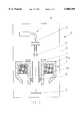
- FIG. 1shows a schematic representation of an electron beam device according to the invention.
- FIG. 2shows a partial sectional view of the apparatus according to the invention for generating an electron beam.
- FIG. 3shows a schematic overall view of the apparatus for generating an electron beam
- FIG. 4shows a schematic view of the means for generating circularly polarised light.
- FIG. 1shows an electron beam device 1 with which a focused electron beam 2 can be generated in an optical column 3.
- This column 4essentially has, in addition to a large number of magnetic and/or electric lenses and apertures (which are not shown here) for beam shaping, an apparatus 4 for generating the electron beam 2, an objective lens 5 for focusing the electron beam onto a specimen 6 and a detector 7 for detecting the secondary or backscattered electrons released on the specimen.
- the objective lens 5a deflecting system 8 is provided in order to deflect the electron beam 2, as is necessary for example during scanning of the specimen 6.
- the objective lensitself is constructed as an electromagnetic lens with a magnetic lens 5a and an electrostatic lens 5b.
- the apparatus 4is formed by a field-assisted photocathode 40.
- One end of an optical waveguide 41is shaped as a tip, provided in the region of its tip with a coating 43, and is used as the emitter.
- the radius of this tipis advantageously between 0.05 and 1.0 ⁇ m.
- a light source 42is coupled on the other end of the optical waveguide 41 in a suitable manner.
- the optical waveguide 41is for example formed by a glass fibre with a core 41a and a cladding 41b.
- a metal carbidesuch as for example CrC or TiC, is used for the coating 43.
- the electron work functions of such metal carbide layersare less than 4 eV and thus are substantially lower than the work functions of the materials such as gold or tungsten which are usually used.
- the coatingis also required to have a sufficiently high conductivity and adequate transparency. Furthermore, it must adhere firmly to the optical waveguide and have a high mechanical hardness.
- the field-generating meansare formed for example by an extraction electrode 44 which is positively charged with respect to the cathode 40.
- the work functionis locally lowered in the region of the cathode tip so far that the visible light fed in from the light source 42 generates a photoemission current.
- anode 45which, depending upon the application, is kept at a higher or lower potential than that of the extraction electrode 44. In one case the released electrons are further decelerated.
- the light source 42feeds light with a wavelength of 200 to 800 nm into the optical waveguide 41.
- So-called laser diodescan be used particularly advantageously as light sources 42 within the scope of the invention for this wavelength range.
- Laser diodesare distinguished over conventional gas and solid state lasers particularly by small dimensions, high efficiency for the light generation, ability to be directly modulated up to high frequencies and low power consumption.
- the light generated by the light source 42is fed into the optical waveguide 41 by means of an optical adapter 46 and a lens 47, for example a "GRIN lens".
- the actual cathode 40is arranged inside a vacuum chamber 48, the light can easily be fed outside this vacuum chamber into the optical waveguide 41.
- the optical waveguide 41must merely be introduced into the vacuum chamber 48 by way of a suitable sealing sleeve 49.
- the laser power which can be appliedis limited to a few mW because of the heating of the tip.
- laser diodesare particularly suitable for generating short light pulses, increased illumination intensities can be used in such short pulses.
- light pulses with high intensitycan be generated in the picosecond range.
- These light pulsesare generated with a pulsing arrangement which is not shown in greater detail.
- This pulsing arrangementis coupled to a blanking system 9 (FIG. 1) in order to achieve blanking of the electrons merely released by field emission, which causes a background current.
- FIG. 4shows means for generating circularly polarised light. They consist essentially of a polariser 50, which linearly polarises the light generated by the laser diode 42. In the subsequent arrangement 51 the incident linearly polarised light is divided into two linearly polarised components which are perpendicular to one another and displaced by ⁇ /4. Such an arrangement 51 can be formed for example by a so-called Soleil compensator. With equal amplitude circularly polarised light is produced.
- the polarised electrons which can be generated with circularly polarised lightcan be used particularly advantageously with electron beam devices in order to image domain structures on ferromagnetic surfaces.
Landscapes
- Chemical & Material Sciences (AREA)
- Analytical Chemistry (AREA)
- Electron Sources, Ion Sources (AREA)
- Common Detailed Techniques For Electron Tubes Or Discharge Tubes (AREA)
Abstract
Description
Claims (12)
Applications Claiming Priority (2)
| Application Number | Priority Date | Filing Date | Title |
|---|---|---|---|
| EP96115830AEP0834896B1 (en) | 1996-10-02 | 1996-10-02 | Apparatus for generating an electron beam |
| DE96115830.0 | 1996-10-02 |
Publications (1)
| Publication Number | Publication Date |
|---|---|
| US5808309Atrue US5808309A (en) | 1998-09-15 |
Family
ID=8223258
Family Applications (1)
| Application Number | Title | Priority Date | Filing Date |
|---|---|---|---|
| US08/932,119Expired - Fee RelatedUS5808309A (en) | 1996-10-02 | 1997-09-17 | Apparatus for generating an electron beam |
Country Status (4)
| Country | Link |
|---|---|
| US (1) | US5808309A (en) |
| EP (1) | EP0834896B1 (en) |
| JP (2) | JPH10125268A (en) |
| DE (1) | DE69621803T2 (en) |
Cited By (3)
| Publication number | Priority date | Publication date | Assignee | Title |
|---|---|---|---|---|
| EP1403898A2 (en) | 2002-09-26 | 2004-03-31 | LEO Elektronenmikroskopie GmbH | Electron beam source, electron-optical apparatus comprising an electron beam source and method of operating an electron beam source |
| US20050006582A1 (en)* | 2003-04-17 | 2005-01-13 | Leo Elektronenmikroskopie Gmbh | Electron microscopy system, electron microscopy method and focusing system for charged particles |
| US9070527B2 (en) | 2011-02-25 | 2015-06-30 | Param Corporation | Electron gun and electron beam device |
Families Citing this family (3)
| Publication number | Priority date | Publication date | Assignee | Title |
|---|---|---|---|---|
| JP5026858B2 (en)* | 2007-05-18 | 2012-09-19 | ナノフォトン株式会社 | Electron gun, electron generation method, and polarization control element |
| DE102008038427A1 (en)* | 2008-08-19 | 2010-02-25 | Ludwig Maximilians Universität | X-ray source |
| JP5709922B2 (en)* | 2013-03-29 | 2015-04-30 | 株式会社Param | Electron gun and electron beam device |
Citations (5)
| Publication number | Priority date | Publication date | Assignee | Title |
|---|---|---|---|---|
| US4868380A (en)* | 1988-03-02 | 1989-09-19 | Tektronix, Inc. | Optical waveguide photocathode |
| EP0348611A2 (en)* | 1988-07-01 | 1990-01-03 | International Business Machines Corporation | Fibre optic photocathode |
| US5041724A (en)* | 1988-11-24 | 1991-08-20 | Ict Integrated Circuit Testing Gesellschaft Fur, Halbleit Erpruftechnik Mbh | Method of operating an electron beam measuring device |
| EP0445787A1 (en)* | 1990-03-06 | 1991-09-11 | Ebara Research Co., Ltd. | Photoelectron emitting member and uses thereof |
| US5289004A (en)* | 1990-03-27 | 1994-02-22 | Olympus Optical Co., Ltd. | Scanning probe microscope having cantilever and detecting sample characteristics by means of reflected sample examination light |
Family Cites Families (1)
| Publication number | Priority date | Publication date | Assignee | Title |
|---|---|---|---|---|
| DE3200496A1 (en)* | 1981-12-31 | 1983-07-21 | Haberkern, Ottmar, 6200 Wiesbaden | Picture-tube design for generating colour television pictures |
- 1996
- 1996-10-02EPEP96115830Apatent/EP0834896B1/ennot_activeExpired - Lifetime
- 1996-10-02DEDE69621803Tpatent/DE69621803T2/ennot_activeExpired - Fee Related
- 1997
- 1997-09-17USUS08/932,119patent/US5808309A/ennot_activeExpired - Fee Related
- 1997-09-22JPJP9256556Apatent/JPH10125268A/enactivePending
- 2001
- 2001-09-26JPJP2001294784Apatent/JP2002116299A/ennot_activeWithdrawn
Patent Citations (5)
| Publication number | Priority date | Publication date | Assignee | Title |
|---|---|---|---|---|
| US4868380A (en)* | 1988-03-02 | 1989-09-19 | Tektronix, Inc. | Optical waveguide photocathode |
| EP0348611A2 (en)* | 1988-07-01 | 1990-01-03 | International Business Machines Corporation | Fibre optic photocathode |
| US5041724A (en)* | 1988-11-24 | 1991-08-20 | Ict Integrated Circuit Testing Gesellschaft Fur, Halbleit Erpruftechnik Mbh | Method of operating an electron beam measuring device |
| EP0445787A1 (en)* | 1990-03-06 | 1991-09-11 | Ebara Research Co., Ltd. | Photoelectron emitting member and uses thereof |
| US5289004A (en)* | 1990-03-27 | 1994-02-22 | Olympus Optical Co., Ltd. | Scanning probe microscope having cantilever and detecting sample characteristics by means of reflected sample examination light |
Cited By (7)
| Publication number | Priority date | Publication date | Assignee | Title |
|---|---|---|---|---|
| EP1403898A2 (en) | 2002-09-26 | 2004-03-31 | LEO Elektronenmikroskopie GmbH | Electron beam source, electron-optical apparatus comprising an electron beam source and method of operating an electron beam source |
| DE10245052A1 (en)* | 2002-09-26 | 2004-04-08 | Leo Elektronenmikroskopie Gmbh | Electron beam source and electron optical apparatus with one |
| US20040124365A1 (en)* | 2002-09-26 | 2004-07-01 | Leo Elektronenmikroskopie Gmbh | Electron beam source, electron optical apparatus using such beam source and method of operating an electron beam source |
| US6828565B2 (en) | 2002-09-26 | 2004-12-07 | Leo Elektronenmikroskopie Gmbh | Electron beam source, electron optical apparatus using such beam source and method of operating and electron beam source |
| US20050006582A1 (en)* | 2003-04-17 | 2005-01-13 | Leo Elektronenmikroskopie Gmbh | Electron microscopy system, electron microscopy method and focusing system for charged particles |
| US6949744B2 (en) | 2003-04-17 | 2005-09-27 | Carl Zeiss Nts Gmbh | Electron microscopy system, electron microscopy method and focusing system for charged particles |
| US9070527B2 (en) | 2011-02-25 | 2015-06-30 | Param Corporation | Electron gun and electron beam device |
Also Published As
| Publication number | Publication date |
|---|---|
| EP0834896B1 (en) | 2002-06-12 |
| DE69621803T2 (en) | 2003-01-16 |
| EP0834896A1 (en) | 1998-04-08 |
| JPH10125268A (en) | 1998-05-15 |
| DE69621803D1 (en) | 2002-07-18 |
| JP2002116299A (en) | 2002-04-19 |
Similar Documents
| Publication | Publication Date | Title |
|---|---|---|
| EP0873573B1 (en) | Electron sources utilizing negative electron affinity photocathodes with ultra-small emission areas | |
| US4442355A (en) | Device for detecting secondary electrons in a scanning electron microscope | |
| EP2686864B1 (en) | Electron beam apparatus | |
| US20030042434A1 (en) | Multiple electron beam lithography system with multiple beam modulated laser illumination | |
| JPH08212952A (en) | Laser irradiation type electron gun | |
| US5808309A (en) | Apparatus for generating an electron beam | |
| GB2081501A (en) | Device for detecting secondary electrons in a scanning electron microscope | |
| US6759800B1 (en) | Diamond supported photocathodes for electron sources | |
| JPH10302705A (en) | Scanning electron microscope | |
| US3946268A (en) | Field emission gun improvement | |
| EP1155419B1 (en) | "x-ray microscope having an x-ray source for soft x-rays | |
| US4918358A (en) | Apparatus using charged-particle beam | |
| US6399934B1 (en) | Optical coupling to gated photocathodes | |
| US3931519A (en) | Field emission electron gun | |
| JP4915786B2 (en) | Electron beam generator and laser beam irradiation method for cathode tip | |
| EP0348611B1 (en) | Fibre optic photocathode | |
| US3931517A (en) | Field emission electron gun | |
| US20240412938A1 (en) | Semiconducting cold photocathode device using electric field to control the electron affinity | |
| US3925664A (en) | Field emission electron gun | |
| Wołowski et al. | Investigations of ion emission from picosecond laser-produced Al plasma | |
| JPH01169858A (en) | Charged particle beam device | |
| JPS6227630A (en) | Cathodoluminescence device | |
| JP2004101185A (en) | Image adjusting apparatus and image adjusting method for X-ray microscope | |
| JPS59229519A (en) | scanning photon microscope |
Legal Events
| Date | Code | Title | Description |
|---|---|---|---|
| FEPP | Fee payment procedure | Free format text:PAYOR NUMBER ASSIGNED (ORIGINAL EVENT CODE: ASPN); ENTITY STATUS OF PATENT OWNER: LARGE ENTITY | |
| AS | Assignment | Owner name:ACT ADVANCED CIRCUIT TESTING GESELLSCHAFT FUR TEST Free format text:ASSIGNMENT OF ASSIGNORS INTEREST;ASSIGNORS:SPEHR, RAINER;SCHMITT, MICHAEL;FROSIEN, JURGEN;REEL/FRAME:008913/0128 Effective date:19971222 | |
| FEPP | Fee payment procedure | Free format text:PAT HOLDER NO LONGER CLAIMS SMALL ENTITY STATUS, ENTITY STATUS SET TO UNDISCOUNTED (ORIGINAL EVENT CODE: STOL); ENTITY STATUS OF PATENT OWNER: LARGE ENTITY | |
| FPAY | Fee payment | Year of fee payment:4 | |
| AS | Assignment | Owner name:ADVANTEST CORPORATION, JAPAN Free format text:ASSIGNMENT OF ASSIGNORS INTEREST;ASSIGNOR:ACT ADVANCED CIRCUIT TESTING GESELLSCHAFT FUR TESTSYSTEMENTWICKLUNG MGH;REEL/FRAME:013000/0794 Effective date:20020422 | |
| FEPP | Fee payment procedure | Free format text:PAYER NUMBER DE-ASSIGNED (ORIGINAL EVENT CODE: RMPN); ENTITY STATUS OF PATENT OWNER: LARGE ENTITY Free format text:PAYOR NUMBER ASSIGNED (ORIGINAL EVENT CODE: ASPN); ENTITY STATUS OF PATENT OWNER: LARGE ENTITY | |
| FEPP | Fee payment procedure | Free format text:PAYOR NUMBER ASSIGNED (ORIGINAL EVENT CODE: ASPN); ENTITY STATUS OF PATENT OWNER: LARGE ENTITY Free format text:PAYER NUMBER DE-ASSIGNED (ORIGINAL EVENT CODE: RMPN); ENTITY STATUS OF PATENT OWNER: LARGE ENTITY | |
| FPAY | Fee payment | Year of fee payment:8 | |
| FEPP | Fee payment procedure | Free format text:PAYOR NUMBER ASSIGNED (ORIGINAL EVENT CODE: ASPN); ENTITY STATUS OF PATENT OWNER: LARGE ENTITY | |
| REMI | Maintenance fee reminder mailed | ||
| LAPS | Lapse for failure to pay maintenance fees | ||
| STCH | Information on status: patent discontinuation | Free format text:PATENT EXPIRED DUE TO NONPAYMENT OF MAINTENANCE FEES UNDER 37 CFR 1.362 | |
| FP | Lapsed due to failure to pay maintenance fee | Effective date:20100915 |