US5806070A - Device and method for controlling solid-state memory system - Google Patents
Device and method for controlling solid-state memory systemDownload PDFInfo
- Publication number
- US5806070A US5806070AUS08/931,193US93119397AUS5806070AUS 5806070 AUS5806070 AUS 5806070AUS 93119397 AUS93119397 AUS 93119397AUS 5806070 AUS5806070 AUS 5806070A
- Authority
- US
- United States
- Prior art keywords
- memory
- address
- data
- controller
- array
- Prior art date
- Legal status (The legal status is an assumption and is not a legal conclusion. Google has not performed a legal analysis and makes no representation as to the accuracy of the status listed.)
- Expired - Lifetime
Links
Images


Classifications
- G—PHYSICS
- G11—INFORMATION STORAGE
- G11C—STATIC STORES
- G11C5/00—Details of stores covered by group G11C11/00
- G11C5/02—Disposition of storage elements, e.g. in the form of a matrix array
- G11C5/04—Supports for storage elements, e.g. memory modules; Mounting or fixing of storage elements on such supports
- G—PHYSICS
- G06—COMPUTING OR CALCULATING; COUNTING
- G06F—ELECTRIC DIGITAL DATA PROCESSING
- G06F12/00—Accessing, addressing or allocating within memory systems or architectures
- G06F12/02—Addressing or allocation; Relocation
- G06F12/06—Addressing a physical block of locations, e.g. base addressing, module addressing, memory dedication
- G06F12/0646—Configuration or reconfiguration
- G06F12/0669—Configuration or reconfiguration with decentralised address assignment
- G06F12/0676—Configuration or reconfiguration with decentralised address assignment the address being position dependent
- G—PHYSICS
- G06—COMPUTING OR CALCULATING; COUNTING
- G06F—ELECTRIC DIGITAL DATA PROCESSING
- G06F13/00—Interconnection of, or transfer of information or other signals between, memories, input/output devices or central processing units
- G06F13/14—Handling requests for interconnection or transfer
- G06F13/16—Handling requests for interconnection or transfer for access to memory bus
- G06F13/1668—Details of memory controller
- G—PHYSICS
- G06—COMPUTING OR CALCULATING; COUNTING
- G06F—ELECTRIC DIGITAL DATA PROCESSING
- G06F13/00—Interconnection of, or transfer of information or other signals between, memories, input/output devices or central processing units
- G06F13/38—Information transfer, e.g. on bus
- G06F13/42—Bus transfer protocol, e.g. handshake; Synchronisation
- G06F13/4204—Bus transfer protocol, e.g. handshake; Synchronisation on a parallel bus
- G06F13/4234—Bus transfer protocol, e.g. handshake; Synchronisation on a parallel bus being a memory bus
- G06F13/4243—Bus transfer protocol, e.g. handshake; Synchronisation on a parallel bus being a memory bus with synchronous protocol
- G—PHYSICS
- G06—COMPUTING OR CALCULATING; COUNTING
- G06F—ELECTRIC DIGITAL DATA PROCESSING
- G06F3/00—Input arrangements for transferring data to be processed into a form capable of being handled by the computer; Output arrangements for transferring data from processing unit to output unit, e.g. interface arrangements
- G06F3/06—Digital input from, or digital output to, record carriers, e.g. RAID, emulated record carriers or networked record carriers
- G06F3/0601—Interfaces specially adapted for storage systems
- G06F3/0602—Interfaces specially adapted for storage systems specifically adapted to achieve a particular effect
- G06F3/061—Improving I/O performance
- G06F3/0613—Improving I/O performance in relation to throughput
- G—PHYSICS
- G06—COMPUTING OR CALCULATING; COUNTING
- G06F—ELECTRIC DIGITAL DATA PROCESSING
- G06F3/00—Input arrangements for transferring data to be processed into a form capable of being handled by the computer; Output arrangements for transferring data from processing unit to output unit, e.g. interface arrangements
- G06F3/06—Digital input from, or digital output to, record carriers, e.g. RAID, emulated record carriers or networked record carriers
- G06F3/0601—Interfaces specially adapted for storage systems
- G06F3/0628—Interfaces specially adapted for storage systems making use of a particular technique
- G06F3/0655—Vertical data movement, i.e. input-output transfer; data movement between one or more hosts and one or more storage devices
- G06F3/0659—Command handling arrangements, e.g. command buffers, queues, command scheduling
- G—PHYSICS
- G06—COMPUTING OR CALCULATING; COUNTING
- G06F—ELECTRIC DIGITAL DATA PROCESSING
- G06F3/00—Input arrangements for transferring data to be processed into a form capable of being handled by the computer; Output arrangements for transferring data from processing unit to output unit, e.g. interface arrangements
- G06F3/06—Digital input from, or digital output to, record carriers, e.g. RAID, emulated record carriers or networked record carriers
- G06F3/0601—Interfaces specially adapted for storage systems
- G06F3/0668—Interfaces specially adapted for storage systems adopting a particular infrastructure
- G06F3/0671—In-line storage system
- G06F3/0673—Single storage device
- G06F3/0679—Non-volatile semiconductor memory device, e.g. flash memory, one time programmable memory [OTP]
- G—PHYSICS
- G11—INFORMATION STORAGE
- G11C—STATIC STORES
- G11C5/00—Details of stores covered by group G11C11/00
- G—PHYSICS
- G11—INFORMATION STORAGE
- G11C—STATIC STORES
- G11C5/00—Details of stores covered by group G11C11/00
- G11C5/06—Arrangements for interconnecting storage elements electrically, e.g. by wiring
- G11C5/066—Means for reducing external access-lines for a semiconductor memory clip, e.g. by multiplexing at least address and data signals
- G—PHYSICS
- G11—INFORMATION STORAGE
- G11C—STATIC STORES
- G11C8/00—Arrangements for selecting an address in a digital store
- G11C8/12—Group selection circuits, e.g. for memory block selection, chip selection, array selection
- Y—GENERAL TAGGING OF NEW TECHNOLOGICAL DEVELOPMENTS; GENERAL TAGGING OF CROSS-SECTIONAL TECHNOLOGIES SPANNING OVER SEVERAL SECTIONS OF THE IPC; TECHNICAL SUBJECTS COVERED BY FORMER USPC CROSS-REFERENCE ART COLLECTIONS [XRACs] AND DIGESTS
- Y02—TECHNOLOGIES OR APPLICATIONS FOR MITIGATION OR ADAPTATION AGAINST CLIMATE CHANGE
- Y02D—CLIMATE CHANGE MITIGATION TECHNOLOGIES IN INFORMATION AND COMMUNICATION TECHNOLOGIES [ICT], I.E. INFORMATION AND COMMUNICATION TECHNOLOGIES AIMING AT THE REDUCTION OF THEIR OWN ENERGY USE
- Y02D10/00—Energy efficient computing, e.g. low power processors, power management or thermal management
Definitions
- This inventionrelates generally to a device and method for electronic data communication and particularly that between a memory controller and an array of memory chips.
- serial linkbetween two systems in order to reduce the number of cables therebetween, as well as the size of the cables, backplanes, and circuit boards in the systems.
- physical densitycan be dramatically improved over conventional methods, in that circuit boards can be made smaller and the total physical volume required for the connecting systems can be reduced.
- serial connectionsare usually slower than their parallel counterparts.
- an array of solid-state memory devicesare in communication with and under the control of a controller module via a device bus with minimum lines.
- Command, address and data informationare serialized and multiplexed before being transferred between the controller module and the memory subsystem.
- the serialized informationis accompanied by a control signal to help sort out the multiplexed components.
- a circuit on each memory device of the subsysteminterprets the serialized bits of information as a pointer code. After the control signal is deasserted, each device routes subsequent bits of the serialized information to the appropriate command, address or data registers according to the type of information pointed to by the code.
- the present inventionuses a serial link to interconnect between the solid-state memory devices and the controller module.
- the serial linkgreatly reduces the number of interconnections and the number of external pads for each device, thereby reducing cost. Also expansion of the memory capacity of the system is simply achieved by a higher packing density of devices on standard printed circuit boards. It is not necessary to have a variety of circuit boards for each density, since the number of address and chip select signals does not change with capacity.
- An important aspect of the inventionis to employ a broadcast select scheme to select or enable a given memory device chip among an array of chips in a memory board or memory module.
- Each memory device chiphas a multi-bit set of pinouts that is connected internally to a device select circuit and externally to a multi-bit mount on the memory module's backplane.
- Each multi-bit mount on the backplaneis preconfigured or keyed to a given address (represented by a multi-bit combination of "0"'s and "1"'s) according to its location in the array.
- the terminals in the multi-bit mount corresponding to the "0" bitare set to ground potential.
- the address of the array as defined by the mount keyis passed onto the device select circuit of the chip.
- the correct array address for that chipis sent to all the chips in the array via the interconnecting serial bus. This address is compared at each chip with that acquired from each chip's mount, and the chip that matched is selected or enabled by its device select circuit. A memory chip remains selected until explicitly deselected, allowing more than one memory chip to be enabled at a time.
- the inventionprovides a simple scheme for assigning an array address to each of the chips mounted on a memory module's backplane.
- the memory chipscan be made generic. This also avoids the need for using conventional individual chip select to enable each memory chip. This results in very low pin count in multi-chip modules, especially that of socketed modules, enabling high density packing of memory chips on memory modules.
- the array of memory chipsmay be distributed over a plurality of memory modules.
- Each of the memory modulescan be enabled by a module select signal from the controller module.
- each memory modulemay be further partitioned into a plurality of memory submodules. These submodules may be mounted on a memory module's backplane and are all enabled by the same module select signal.
- the multi-bit address in the multi-bit mount for each memory deviceis partitioned into two subsets. The permutations of one subset are used to provide the different memory-device addresses on a memory submodule. The permutations of the other subset are used to provide the different memory-submodule addresses on a memory module.
- one particular key among the permutations of the multi-bit mountsis reserved as a "master key” to unconditionally have each device select circuit enable its chip.
- this "master key”is given by having all the bits of a multi-bit mount not grounded. This allows a group of chips with this "master key” mount to be selected together.
- the broadcast select schemehas a reserved code that can be communicated to the array of memory chips on the backplane in order to deselect all previously selected chips.
- a select sequence of shifting in a pattern of all onesresults in a global deselect.
- Another important aspect of the inventionis to implement a streaming read scheme to improve the read access of the memory system. While a chunk (e.g. 64 bits) of data is being read from the memory cells, serialized and shifted out of a memory chip, the address for the next chunk is being setup and sent to the memory chip to begin accessing the next chunk of data.
- the overlapping operations of reading out of one chunk of data and staging for the access of the next chunk of datagreatly improve the read access speed of the memory system.
- serial linkis unconventional for integrated circuit memory chips. These memory devices are typically random-access memories which are designed for high speed access and therefore employ parallel address and data buses. Serializing the command, address and data information for these devices is unconventional since it may require more circuitry than conventional parallel access, and may result in slower access.
- the present inventionwhen used in a block transfer regime (e.g., reading 4096 consecutive bits at a time, is relatively insensitive to access time, the speed being determined largely by the data throughput once reading has begun.
- the present inventionrecognizes that employment of a serial link in the present electrically erasable programmable read only memory (“EEPROM”) system architecture, particularly with the features of broadcast selection and streaming read, results in simplified connections therein without compromising access speed for the intended application.
- EEPROMelectrically erasable programmable read only memory
- FIG. 1Ais a general microprocessor system connected via a bus interface to a solid-state mass storage system according to a preferred embodiment of the present invention
- FIG. 1Bis a general microprocessor system connected directly via a system bus to a solid-state mass storage system according to another preferred embodiment of the present invention
- FIG. 2Aillustrates schematically the solid-state memory module arranged as an array of memory devices mounted on "keyed" mounts in a memory board backplane;
- FIG. 2Billustrates schematically another memory module arrangement in which a plurality of memory submodules are being mounted on "keyed” mounts on the backplane of the solid-state memory module, and a plurality of memory devices is being mounted on "keyed” mounts on each memory submodule;
- FIG. 3illustrates a "radial select" configuration of the memory devices in FIG. 2 in which the mounts all have the master, all-bits-ungrounded “keys", and each memory device is selected by an individual chip select (CS*) signal;
- CS*chip select
- FIG. 4is a schematic illustration of the functional blocks of a flash EEPROM memory device
- FIG. 5Ashows one embodiment of the device select circuit within the memory device illustrated in FIG. 4;
- FIG. 5Bis a timing diagram for the device select circuit of FIG. 5A;
- FIG. 6Ais one embodiment of the serial protocol logic within the memory device illustrated in FIG. 4;
- FIG. 6Bis a timing diagram for the serial protocol logic of FIG. 6A;
- FIG. 6Cshows the logic state of signals in the device select circuit shown in FIGS. 4-6.
- FIG. 7Ais a schematic illustration of the functional blocks of the controller module illustrated in FIG. 1A;
- FIG. 7Bis a schematic illustration of the functional blocks of the alternative controller module illustrated in FIG. 1B;
- FIG. 8Ais a schematic illustration of the functional blocks of the memory controller illustrated in FIG. 7A;
- FIG. 8Bis a schematic illustration of the functional blocks of the memory controller illustrated in FIG. 7B.
- FIG. 9is a timing diagram for the read streaming scheme, according to a preferred embodiment of the present invention.
- Table 1shows the logic of the device select circuit in FIGS. 4-6.
- FIG. 1AA typical computer system in which the various aspects of the present invention are incorporated is illustrated generally in FIG. 1A.
- a typical computer system 101has an architecture that includes a microprocessor 121 connected to a system bus 123, along with, main system memory 125, and at least one or more input-output devices 127, such as a keyboard, monitor, modem and the like.
- Another main computer system component that is connected to a typical computer system bus 123is a large amount of long-term, non-volatile memory 129.
- a mass storageis a disk drive with a capacity of tens of megabytes of data storage.
- data from this mass storage 129is retrieved into the volatile RAM of main system memory 125 for processing, and new or updated data can be easily written back to the mass storage.
- One aspect of the present inventionis the substitution of a specific type of semiconductor memory system for the disk drive without having to sacrifice non-volatility, ease of erasing and rewriting data into the memory, speed of access, and reliability. This is accomplished by employing an array of non-volatile, solid-state memory, integrated circuit chips. This type of memory has additional advantages of requiring less power to operate, and of being lighter in weight than a hard disk drive memory, thereby being especially suited for battery-operated portable computers.
- the integrated circuit mass storage memory 129includes one or more solid-state memory modules such as 131, 132 under the control of a controller module 133. Addresses, data, and commands are communicated between the memory modules 131, 132 and the controller module 133 by means of a device bus 135.
- the one or more memory modules such as 131, 132can be selectively enabled by individual module select signals such as MS1*, MS2*. These signals are carried in select lines such as 151, 152 from the controller module to individual memory modules.
- the controller module 135is connected to a standard computer bus standard computer bus interface 137 via an interface bus 138.
- the interface 137is connected on the other hand to the computer system via the standard computer system bus 123.
- the mass storage memoryis adapted to be powered by a standard power supply within the computer system.
- the bus interface 137is preferably an IDE (Integrated Device Electronics) controller.
- FIG. 1Billustrates an alternative embodiment in which the controller module 134 is connected directly to the system bus 123 of the computer system 101.
- the controller module 134is simplified as some of its functions are performed by the system microprocessor 121 and other system resources.
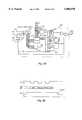
- FIG. 2Aillustrates schematically the solid-state memory module such as 131 or 132 of FIGS. 1A and 1B arranged as an array of memory devices 141 mounted on a printed circuit memory board or a backplane 143.
- Each memory device 141is an integrated circuit memory chip.
- Each memory device 141has two groups of external pads or pinouts.
- the first groupis the device-bus pinouts 145 for connection to the device bus 135 on the backplane 143.
- the device bus 135interconnects all the memory devices 141 in the solid-state memory module 131 on the one hand, and the controller module 133 or 134 on the other hand (see FIGS. 1A-1B and 2A-2B).
- the second group of external padsare device-select pinouts 147 which are to be connected to corresponding pads of a mount 149 on the backplane 143. There is one such mount for each memory device so that the memory devices 141 are laid out in an array in the backplane 143.
- the mounts in the arraywill have grounding configurations (11111), (11110), (11101), . . . , (00000), where "0" denotes a pad that is grounded.
- these keyed mountsare used to assign an array address to the memory device chip 141 mounted thereon. In this way each memory device chip can be addressed for selection or enablement.
- FIG. 2Billustrates schematically another memory module arrangement in which each memory module such as 131 may be further partitioned into a plurality of memory submodules such as 181, 182.
- Thisallows for more flexibility in memory configurations without the need to provide at the outset the full capacity of mounts for all possible memory devices 141 in the memory module's backplane 143. In this way, the backplane 143 needs only provide a reduced set of mounts and spaces for these submodules.
- Each submodule such as 181, 182has a smaller group of memory devices 141 mounted on it and they are all enabled by the same module select signal MS1* 151.
- each memory device 141is given an address on the memory submodule 181 by means of the grounding configuration of the multi-pin mount 149.
- the memory devices in a submoduleonly a subset of the bits of the multi-pin mount is required.
- only two bits of the multi-pin mount 149need be configured to provide unique addresses on each submodule.
- the rest of the bits in the multi-pin mount 149may be configured to provide unique addresses for the memory submodules such as 181, 182 on the backplane 143 of the memory module 131.
- For a 5-bit mounttwo of the bits are configured for four memory-device addresses on each memory submodule, and the other three bits are configured for up to eight memory-submodule addresses on the memory module's backplane 143.
- the memory submodules such as 181, 182are each mounted on the memory module's backplane 143 with connections to the device bus 135 and to a submodule multi-pin mount 189.
- This mount 189is a subset of a memory-device's multi-pin mount 149. For the example above, it will be a 3-pin mount.
- one particular "key” among the permutations of grounding configurations of the multi-bit mounts 149is reserved as a "master select" which unconditionally allows each chip to be selected or enabled.
- FIG. 3illustrates a radial select scheme, in which all the memory devices 141 in the solid-state memory module 131 can be enabled for selection by a master select configuration.
- this "master select"is given by having all the bits of the mount not grounded.
- each mount 149 in the arrayhas the same grounding configuration, namely (11111).
- Individual memory devices within the solidstate memory module 131are selected by dedicated chip select signals such as CS1*, CS2*, CS31* as in the conventional case. These dedicated chip select signals are respectively carried in additional lines such as 171, 172, 175 among the device bus 135.
- non-volatile, solid-state memory, integrated circuit chipsexamples include read-only-memory (ROM), electrically-programmable-read-only-memory (EPROM), electrically-erasable-programmable-read-only-memory (EEPROM), and flash EEPROM.
- ROMread-only-memory
- EPROMelectrically-programmable-read-only-memory
- EEPROMelectrically-erasable-programmable-read-only-memory
- flash EEPROMflash EEPROM
- an array of flash electrically-erasable-programmable-read-only memoriesin the form of an integrated circuit chip is employed as the memory device 141.
- a flash EEPROM deviceis a non-volatile memory array which may be partitioned into one or more sectors. These sectors are addressable for electrical erasing of all memory cells therein.
- Various details of flash EEPROM cells and systems incorporating defect managementhave been disclosed in related co-pending U.S. patent applications. They are copending U.S. patent applications, Ser. No. 508,273, filed Apr. 11, 1990, by Mehrotra et al., now U.S. Pat. No. 5,172,338, Ser. No. 337,566, filed Apr.
- FIG. 4is a schematic illustration of the functional blocks of a flash. EEPROM device.
- the flash EEPROM device 141includes an addressable flash EEPROM cell array 201, a device select circuit 203, a serial protocol logic 205, a power control circuit 207, and various WRITE, READ, ERASE circuits, compare and shift register 211, 213, 215, 217 and 219.
- serial linkbetween each of the memory devices 141 and the controller module 133 or 134.
- the serial linkcarries serialized addresses, data and commands. This has several advantages in the present application.
- the serial linkgreatly reduces the number of interconnecting lines between the controller module 133 or 134 and each of the memory devices 141. Fewer signal lines requires fewer traces on the printed circuit memory boards or backplanes 143, resulting in dramatic savings in board space and overall system density improvements. Fewer pins are required. This applies both to memory card edge connectors and to individual memory device chip pinouts. The results of fewer pins are lower costs and greater system reliability. Also fewer pinouts on a memory device results in a smaller device and consequently, lower device cost.
- the flash EEPROM memory device 141has two sets of external pins.
- the first set of external pinsis for connection to the device bus 135.
- the device bus 135includes a timing signal line, CLK 231, a control signal line P/D* 235, two serial-In's, SI0 237, SI1 239, two serial-Out's, S00 241, SO1 243, and a set of power lines V1 . . . Vn 245.
- Another control signal line, chip select CS* 171is shown outside the device bus 135, although in some embodiments, it may be regarded as part of the device bus 135.
- the use of two serial-In's and two serial-Out'srequires very few signal lines and yet still allows information to be transferred at adequate rates.
- the second group of external pinsconsists of the five device-select pinouts 147 described in connection with FIGS. 2 and 3.
- any memory device 141 among the array of memory devices mounted on the backplane 143may be enabled such that the device is selected whenever the CS* 171 (chip select) is asserted.
- each devicemay be enabled in one of two ways.
- the firstis master select by means of a special grounding configuration of the device select pins 147, as described earlier in connection with FIG. 3.
- One particular "key” among the permutations of grounding configurations of the multi-bit mounts 149 (see FIG. 3)is reserved as a "master select” which unconditionally allows each chip to be selected or enabled. This allows a group of chips with this "master select" mount to be selected together (see FIG. 3A) or allows for radial selection of individual devices (see FIG. 3B).
- the secondis "address-select" by shifting in an address that matches the one defined by the device select pins 147 from the serial lines SIO 237, SI1 239.
- the address for each location in the arrayis defined by the grounding configuration or "key" of the mount 149 thereat.
- the address defined by the mountis passed onto the memory device 141.
- a device select circuit in each memory device 141compares the array address obtained from the device bus to that obtained from the device select pinouts 147.
- an address deselect schemeis employed in which a special address or code can be shifted in to deselect devices that have previously been selected.
- the special deselect codeis (11111).
- FIG. 6Csummarizes the logic states of signals of the device select circuit 203 which appears in FIGS. 4-6.
- the device select circuithas inputs from the device select pins 147 and the device bus 135, and has an output DS 309 (see FIG. 5A) to select or deselect the device it is controlling.
- FIG. 5Ashows one embodiment of the device select circuit 203 incorporating the master select, address deselect, address deselect features.
- the circuit 203has inputs SI0 237, SI1 239, and the two control lines CS* 171, P/D* 235 from the device bus 135.
- the array address of the memory device 141 in FIG. 4is defined by a 5-bit address. This 5-bit address is set by the mount 149 and communicated to the device select circuit 203 via the deviceselect pinouts 147.
- the master select featureis implemented by the 5-input AND gate 301.
- a pin configuration of (11111)appears, the HIGH output of the AND gate 301 is latched by a master select latch 303. This in turn results in DS 309 becoming HIGH when the chip select CS* in line 171 is LOW, as shown on FIG. 5A.
- Device selection by address-matchingis implemented by a comparator 305 and an address-match latch 307.
- a 5-bit array addressis shifted into a shift register 311 from the serial-in lines SI0 237, SI1 239.
- the clocking signalis carried by the control line P/D* 235 which is gate-enabled by a HIGH signal in the master chip select line CS* 171.
- the 5-bit array addressis then passed from the shift register 311 via the bus 313 to the comparator 305.
- the comparator 305compares this address with that obtained from the device-select pinouts 147.
- the comparator output 306goes HIGH whenever the addresses match. This output is clocked into the address-match register 307 by the falling edge of CS* 171. This results in a S-R register 315 being set HIGH such that DS 309 is also HIGH and the device is selected. On the other hand, when the addresses do not match, DS 309 will be LOW and the device is not selected.
- Device deselection by address deselectwhich is implemented by a special deselect code e.g., (11111) is used to signal global deselection.
- a second 5-input AND gate 317looks for a data pattern of all one's being shifted into the shift register 311. When a match occurs and also the chip select CS* in the line 171 goes from HIGH to LOW (see FIG. 5B), the comparator 317 outputs a deselect signal which is latched by a deselect latch 319. This in turn is used to reset the S-R register 315 on all devices previously selected. By shifting in the (11111) pattern and activating the CS* signal, all devices that are presently selected will see the deselect pattern and will be deselected.
- FIG. 5Bis a timing diagram for the device select circuit of FIG. 5A.
- the CS* signalgoes high and the timing signal P/D* is used to clock the serial address from SI0 and SI1 into the shift register 301.
- the comparator 303After three P/D* clock periods, 6 bits have been loaded into the shift register 301 and only the least significant 5 bits are used by the comparator 303.
- the trailing edge of CS*is used to load the various latches 303, 307, 319.
- a stream of serialized addresses, data and commandsis then passed between the controller module 133 or 134 (see FIGS. 1A and 1B) and the enabled memory device 141 via the device bus 135. From the memory device end, a serial protocol logic is used to sort out, re-organize and re-route the various information in the serial stream to their appropriate destinations.
- FIG. 6Ais one embodiment of the serial protocol logic in the memory device 141 illustrated in FIG. 4.
- the serial protocol logic 205receives inputs from the device bus 135. They are clock signals from the CLK 231 line, control signals from CS* 171, P/D* 235 and serial-in lines SI0 237, SI1 239.
- the serial protocol logic 205essentially sorts out the serialized stream of addresses, data and commands from the serial lines SI0 237 and SI1 239. It then re-routes each type of information before converting some of them into parallel forms for output.
- a pointer shift register 331 and a pointer decode 341are used to direct the non-pointer information in the serial lines SI0 237, SI1 239 to an address shift register 333, a command shift register 335 or a data shift register 337.
- the address shift register 333when enabled, shifts the stream from the serial lines SI0, SI1 out to an 18-bit internal address bus 343.
- the command shift register 335shifts out a parallel command vector which is further decoded by a command decode 344 into a number of control signals such as WRITE, READ, ERASE, . . . , and OTHER carried by control lines 345.
- the data shift register 337shifts in a 64-bit chunk of data, and outputs it in parallel on a WRITE data bus 347.
- the pointer shift register 331is first enabled to receive the routing information. After the routing information is received, the pointer shift register 331 is disabled. The routing information received is decoded by the pointer decode 341 to selectively enable one of the three shift registers 333, 335, 337. Timing and control is provided by the P/D* line 235. One state (HIGH) of P/D* 235 is used to enable the pointer shift register 331 and disable the shift registers 333, 335 and 337. The other state (LOW) of P/D* 235 is used to disable the pointer shift register 331 and enable the shift registers 333, 335 and 337.
- One state (HIGH) of P/D* 235is used to enable the pointer shift register 331 and disable the shift registers 333, 335 and 337.
- the other state (LOW) of P/D* 235is used to disable the pointer shift register 331 and enable the shift registers 333, 335 and 337.
- serial protocol logic 205illustrated in FIG. 6A is best understood with reference to its timing diagrams.
- FIG. 6Bis the corresponding timing diagrams for the operations of the serial protocol logic.
- P/D* 235When P/D* 235 is HIGH, the shift registers 333, 335 and 337 are disabled.
- a stream of 2-bit codes from the two serial lines SI0, SI1are clocked into the pointer shift register 331 at the rising edge of each clock period. Each of these 2-bit codes is used to select and point to one of the shift registers 333, 335 and 337.
- the 2-bit code "00"is reserved for future use.
- Code "01”points to the address shift register 333.
- Code "10”points to the command shift register 335.
- Code "11”points to the data shift register 337.
- the protocolis such that when P/D* 235 goes LOW, the falling edge is used to load the last 2-bit code in the pointer shift register 331 to the pointer decode 341.
- the first falling edge shown (351)loads the code "10" (353) from the pointer shift register 331 to the pointer decode 341. This means the command shift register 335 is pointed to and is selected.
- the pointer shift register 331is again enabled to receive information from the serial lines SI0, SI1.
- the second falling edge shown (361)latches the code "11" (363) into the pointer shift register 331.
- the data shift register 337is now pointed to and is selected.
- the pointer shift register 331is disabled and the information from the serial lines SI0, SI1 are now shifted into the enabled data shift register 337 and interpreted as data.
- the shiftingends when the P/D* line 235 goes HIGH again.
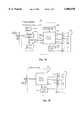
- FIG. 7Ais a schematic illustration of the functional blocks of the controller module illustrated in FIG. 1A.
- the controller module 133contains essentially a memory controller 401 which manages the information flow between the solid-state memory module 131 and the disk drive interface 411. It also sequences various control signals for the operation of the memory devices 141.
- the memory controller 401receives timing clock signals from a clock generator 403. It also controls the output of various voltages required for the operations of the memory devices 141 by means of a power supply or converter 405.
- the device bus 135links the memory controller 401 and the power supply/converter 405 to the memory device 141.
- a standard disk drive interface 411is implemented between the memory controller 401 and the computer system bus 123.
- the controller module 133 and therefore the mass storage 129behaves as if it were a disk drive system. This allows hardware and software compatibility when the present solid-state memory system is used to substitute for a disk drive system.
- the standard disk drive interface 411typically includes a buffer memory 413, a peripheral interface 415 and a controller microprocessor 417.
- the buffer memory 413is essentially a static RAM, and it temporarily holds data that is to be written or that has just been read.
- the peripheral interface 415may be implemented by a commercially available integrated-circuit chip such as the SH 265 Disk controller by Cirrus Logic Inc., Milpitas, Calif.
- the peripheral interface 415exchanges data with the memory controller 401 via a data serial line 421.
- the controller microprocessor 417may be implemented by a commercially available integrated-circuit chip such as the 68HC11 microprocessor by Motorola Inc., Phoenix, Ariz.
- a controller address and control bus 423also interconnects the peripheral interface 415, the memory controller 401 and the controller microprocessor 417.
- FIG. 7Bis a schematic illustration of the functional blocks of the alternative controller module illustrated in FIG. 1B.
- the controller module 134contains essentially a memory controller 431 and a power converter 405.
- the memory controller 431manages the information flow between the solid-state memory module 131 and the computer system 101. It also sequences various control signals for the operation of the memory devices 141. Unlike the controller module 133 of FIG. 7A, some of the controller module's functions are performed by the system microprocessor 121 and other system resources of the computer system 101 (see FIG. 1B).
- the memory controller 431is in direct communication with the system microprocessor 121 via the system bus 123. Similar to the memory controller 401, it also controls the output of various voltages required for the operations of the memory device 141 by means of a power supply or converter 405.
- the device bus 135links the memory controller 431 and the power supply 405 to the memory devices 141.
- FIG. 8Ais a schematic illustration of the functional blocks of the memory controller 401 illustrated in FIG. 7A.
- the memory controller 401is linked to the disk drive interface 411 by means of a serial data line 421 and a controller address and control bus 423.
- the serial data line 421Tracing the data path from the disk drive interface 411 side, the serial data line 421 enters through an I/O port 501 and is converted by a serial-parallel converter (SERDES) 511 to an 8-bit parallel bus. It is then switched by a MUX 515 into a FIFO 517 before being serialized and switched out by a MUX/SERDES 519 to an I/O port 521 as the 2-bit serial-in bus SI0, SI1.
- the data path from the device bus 135 sidehas the 2-bit serial-out bus SO0, S01 tracing a reverse path along the same functional blocks.
- the memory controller 401also has an I/O decode (e.g. register strobe/enable decodes) 531, address control registers 533, an error correction code (ECC) hardware 541, a sequencer 543, and a command shift register 545. Addresses and control signals are carried along the controller address and control bus 423.
- the busenters through the I/O port 501 and lines therein interconnect the various functional blocks as shown in FIG. 8A.
- the ECC hardware 541is used to check and correct errors that may arise in the data (connections not explicitly shown).
- FIGS. 1A, 2 and 7AIn order to describe the operation of the memory controller 401 in relation to the computer system 101, the controller module 133 and the memory module 131, references are also made to FIGS. 1A, 2 and 7A.
- the system microprocessor 121To initiate the reading or writing of a memory device 141, the system microprocessor 121 initializes internal registers (e.g. address control registers 533) and the sequencer 543 for operation.
- internal registerse.g. address control registers 533
- the controller microprocessor 417evaluates the command and translates that command and address to a memory device address and command sequence.
- the memory device's addressis loaded into the address control registers 533 in the memory controller 401.
- the microprocessorthen activates the desired sequence by writing a command vector to the sequencer. This command vector will cause the sequencer to jump to the address value loaded and start executing the code at that address.
- the microprocessorreceives a command over the host interface via the peripheral interface 415 of the controller module 133. It evaluates this command and translates the address to a memory device address. The microprocessor then loads this address into the address control registers 533. The microprocessor then loads the sequencer 543 with the starting address of the read sequence. The sequence starts executing code at this address. The sequencer 543 first shifts out the select address for selecting a particular memory device chip 141, followed by an address of a memory chunk (e.g. 64 bits) from the address control registers through the lines 551 via the MUX/SERDES 519 to the serial-in lines SI0, SI1.
- a memory chunke.g. 64 bits
- the sequencerthen puts out a read command and switches the MUX/SERDES 519 to receive it via the lines 553.
- the read commandis shifted out to the serial-in lines SI0, SI1.
- the sequencer 543is putting out the control signals CS* and P/D* through the command shift registers 545.
- the sequencer 543enables the FIFO 517 to accept incoming data read from the memory device 141. This data is received into registers in the I/O port 521 and converted to parallel data in the MUX/SERDES 519 before being put into the FIFo 517.
- the ECC hardware 541is activated and starts calculating on the data loaded into the FIFO.
- the sequencer 543looks at a FIFO RDY line (not explicitly shown) to see if a byte of data is ready to be sent to the peripheral interface 415 of the disk drive interface 411. When the FIFO 517 is ready, the sequencer 543 signals the peripheral interface 415 to receive the data and then transmits the data from the FIFO 517 via the SERDES 511 out to the serial line 421.
- datais written and read in 64-bit chunks.
- the sequencer 543updates the address control register 533 (chunk counter) and shifts out the address for the next chunk to be read.
- the controllerWhile reading data from memory, the controller will output the address for the next chunk to be read at the same time it is receiving the read data from the present chunk.
- the controllersupports overlapping operations to give a continuous flow of data. This sequence continues until the last data chunk is read as signaled by the address control registers 533 to the sequencer 543. While data is being received from the memory device 141, it is being gated by the sequencer 543 into the ECC hardware for error checking.
- the status of the ECC check as to whether data was received correctlyis then posted to the controller microprocessor 417. After this, the sequencer 543 checks to see if the FIFO 517 has been emptied, and if so, shuts the I/O ports 501, 521 off and gates to an idle state, waiting for a new command.
- the controller microprocessor 417 of the disk drive interface 411has a direct path for reading and writing data to and from the memory device 141 via the controller address and control bus 423 and 561 and the MUX/SERDES 519. This is done to support reading of header information in memory sectors and, formatting and diagnostics of the memory device.
- the controller microprocessor 417 of the disk drive interface 411 in the controller module 133receives a command over the bus interface 138 via the peripheral interface 415 (see also FIGS. 1a, 7a).
- the sequencer 543receive a write vector it will signal and drive an input on the peripheral interface 415 of the disk drive interface 411.
- the peripheral interface 415will then initiate the sequencer 543 to have serial data received over the serial line 421.
- the data received by the serial-parallel converter 511is put in parallel format and written into the FIFO 517 via the MUX 515.
- the addressing of a particular memory device chip and a memory chunk thereinis similar to that described for the read operation.
- the sequencer 543has gated the address loaded in the address control registers 533 to the memory device, including the device chip select address.
- the sequencerwill look at a FIFO RDY line (not explicitly shown) to see if a byte of data is ready to be sent to the memory device 141 via the device bus 135.
- the sequencer 543switches the MUX/SERDES 519 from the address control registers 533 to the FIFO 517 to receive data instead.
- the sequencergates out data in 64-bit chunks, received a byte at a time from the FIFO, and transmits the data via the SERDES/MUX 519 and I/O port 521 out to the Serial-out lines SOO, SO1 of the device bus 135.
- the sequencer 543then switches the MUX/SERDES 519 again to shift out the required command vectors via the bus 553 to the Serial-in lines SIO, SI1.
- the sequencerwill activate the power converter 405 of the controller module 133 by loading the proper values in the power control I/O port registers (not explicitly shown) via a bus 571.
- the outputs of these registersdrive the inputs to the power converter 405 providing the required voltages for the programming (or writing) of the memory device.
- These output linesalso turn on any programming reference current out of the power converter 405.
- sequencer 543handles the control interface to the memory device 141 by outputting control signals CS*, P/D* via the command shift registers 545. Also, the sequencer keeps track of the write time and at the end of it, halts programming by lowering the programming voltage from the power converter 405.
- a 64-bit chunk of datais programmed at a time. After a chunk of data is programmed, the sequencer will then issue a pulse to the address control registers 533 updating the chunk address. It then repeats the sequence for the next chunk to be programmed.
- FIG. 8Bis a schematic illustration of the functional blocks of the alternative memory controller 431 illustrated in FIG. 7B.
- a key feature of this architectureis to have the data that is read or written to be accessed by a host interface 601 used to set up the control. Unlike the embodiment shown in FIG. 8A, this memory controller 431 interfaces directly with the system bus 123 and does not have a bus interface 137 nor a disk drive interface 411 inserted therebetween (see FIG. 1B). Tight interaction with the host microprocessor 121 is required.
- the host interface 601is connected directly to the system bus 123. It includes address registers 605 and a serial-parallel converter (SERDES) 607.
- SERDESserial-parallel converter
- the memory controller 431also includes a read/write control block 611 connected in between the host interface 601 and a memory control block 621. Error correction is performed by ECC hardware 612.
- the read/write (R/W) control block 611further includes a R/W state machine 613, control/status registers 615, a timer interrupt 617, and a power control 619.
- the memory control block 621further includes a memory protocol state machine 623 and a command/data power gating control 625.
- the gating control 625is for gating commands, addresses, data, and also a programming reference current into the device bus 135 (see also FIG. 7B).
- the design of the memory controller 431is based on the two state machines 613 and 623 to handle the hardware control.
- the read/write (R/W) state machine 613handles the high level details of the operations, while the low level protocol state machine 623 is used to handle the details of the interface with the memory device.
- the host microprocessor 121To initiate a write sequence to the memory device 141, the host microprocessor 121 through the host interface 601 writes the desired starting address into the address registers 605. The microprocessor also writes the control/status registers 615 with the code for a particular group of memory devices that is to be turned on for this command.
- the serial-parallel converter 607also contains memory that allows an entire block of data to be buffered between the host and the memory device 141.
- the microprocessor 121then writes the R/W state machine 613 with a vector for a write command.
- the R/W state machine 613selects the address registers 605 as the data source and enables the protocol state machine 623 to begin.
- the protocol state machine 623serially selects the desired memory device chip and shifts in the desired memory cell address.
- the protocol state machine 623also outputs the proper command and starts the shifting of the write data to the memory device. This is done by taking the data out of the serial-parallel converter 607 in a serial manner and directing it through the memory control block 621 to be transferred to the memory device.
- the system microprocessor 121continues to load data into the serial-parallel converter 607 keeping data ready to be shifted to the memory device.
- datais being pulled out of the serial-parallel converter 607 it is also input to the ECC hardware 612 where the clock bits are being generated.
- the protocol state machine 623stops sending data and activates the high programming voltages by setting the proper control bits in the power gating of gating control 625 and power control 619. This in turn drives the power converter 405 of the controller module 134 to output the proper voltages as enabling the programming reference current via serial-in SI0 237.
- the programming voltages and programming reference currentare turned on for a specified duration by the protocol state machine 623 and the sequence is repeated for the next chunk. If data written to the memory device is the last chunk, the ECC hardware 612 is enabled and its data is written to the memory device via the device bus 135 by the normal chunk programming operations.
- status bits from the status registers 605are available to the host microprocessor 121. Examples of such status bits are data ready/empty, ECC errors etc.
- the read sequenceis much like that of write with the flow of data reversed.
- the microprocessor 121loads the starting address into the address registers 605. It then selects the desired group of memory devices by writing the code for them into the control/status registers 615.
- the microprocessorthen issues the read command to the R/W state machine 613. It then activates the protocol state machine 623 which shifts out the address of the memory device, causing the proper chip to be serially selected and the starting address to be loaded into the memory device.
- the protocol state machine 623also shifts out the read command to the selected memory device and also outputs appropriate control signals (e.g. P/D*) to the control lines in the device bus 135.
- the read serial data received from the memory deviceis then directed by the gating control 625 to the serial-parallel converter 607 logic as well as the ECC hardware 612.
- the microprocessor 121then polls a status bit in the status registers 605 to see if a word of data is compiled in the serial-parallel converter 607. When this bit goes active by the proper number of bits being loaded, the microprocessor 121 reads the data from the serial-parallel converter 607 and stores it in the host memory 125. Thus a word of read data at a time is transferred to the host computer system 101.
- the controllerwill output the next address and perform the access delay for the next chunk at the same time the present chunk is being input. This allows for overlapping of access times to get a continuous stream of read bits.
- the ECC bytesare fetched from the ECC hardware 612 and compared with the value recorded in the memory device. If an error occurs, a correction of the data will be attempted. If no error has occurred the R/W controller halts, stopping the protocol state machine 623, and waits for a new command to be entered.
- FIGS. 1A and 1BAn important feature of the present invention as described above is the ability to perform a read streaming function between the memory devices 141 and the controller module 133 or 134 (see FIGS. 1A and 1B).
- the memory device 141supports read streaming by latching 64 bits (chunk) of parallel information into a holding shift register 219 to be shifted out as a serial stream.
- FIG. 9The timing diagram for read streaming is illustrated in FIG. 9, which is to be referred to in conjunction with FIGS. 4, 8A and 8B.
- the module select signal MS*(not shown in FIG. 9)
- the current (nth) chunk (64 bits) of datais read out and is then shifted to the controller module 133 or 134.
- the datais put in deserialized form and stored to be sent over the host interface.
- the memory controller 401 or 431also updates the address for the next ((n+l)th) chunk of data to be read, and sends it to the memory device 141.
- This addressis then used to access the memory device for the next ((n+l)th) chunk of data while the current (nth) chunk of data is still being shifted out.
- the last pair of bits of the current chunkhas been shifted out, the next 64 bits of data are already available at the outputs of 64 sense amplifiers (not shown) of the read circuit 213. This information can then be transferred to the 64 bit serial out shift register 219 without the usual memory access delay.
- This read streaming sequenceis repeated until all data desired by the memory controller 401 or 431 has been fetched from the memory device 141.
- overall system performancecan be improved and the serial data stream is made to look like a continuous bit stream.
- typical memory structuresdo not have read out time overlapping with address and access times.
Landscapes
- Engineering & Computer Science (AREA)
- Theoretical Computer Science (AREA)
- Physics & Mathematics (AREA)
- General Engineering & Computer Science (AREA)
- General Physics & Mathematics (AREA)
- Human Computer Interaction (AREA)
- Microelectronics & Electronic Packaging (AREA)
- Read Only Memory (AREA)
- Dram (AREA)
Abstract
Description
This is a continuation of application Ser. No. 08/396,488, filed Mar. 2, 1995 now abandoned, which is a division of application Ser. No. 07/736,733, filed Jul. 26, 1991 U.S. Pat. No. 5,430,859.
This invention relates generally to a device and method for electronic data communication and particularly that between a memory controller and an array of memory chips.
Conventional memory system design uses a large number of parallel signals for the addressing, data transfer, and control of system operations. This is a very convenient means of configuring memory systems and results in very fast system operation. This is particularly true for integrated circuit, random access memory devices.
A disadvantage arises from this approach in that a large number of signal lines needs to be routed to each and every memory device in the memory system. This entails rather inefficient use of printed circuit board area and large cables and backplanes. Also, the system power supply must have higher capacity in order to deliver higher peak power for parallel signalling. In most cases, however, this inefficiency must be tolerated in order to achieve best possible speed of operation.
In some applications, on the other hand, it is possible to employ a serial link between two systems in order to reduce the number of cables therebetween, as well as the size of the cables, backplanes, and circuit boards in the systems. Overall, physical density can be dramatically improved over conventional methods, in that circuit boards can be made smaller and the total physical volume required for the connecting systems can be reduced. However, serial connections are usually slower than their parallel counterparts.
It is desirable to have simple connections between a memory controller and an array of memory devices, without compromising performance.
Accordingly, it is an object of the present invention to simplify connections between two systems with minimum compromise on performance.
It is another object of the present invention to simplify connections between a controller and an array of solid-state memory devices.
It is another object of the invention to improvements in selecting one or more memory devices within a memory array.
It is also an object of the invention to improvements in deselecting memory devices which have previously been selected.
It is yet another object of the present invention to allow the memory devices of the memory array to be configured so that they are all enabled for simultaneous communication.
It is yet another object of the present invention to improve the speed of the memory devices.
These and additional objects are accomplished by improvements in the architecture of a system comprising a memory controller and an array of solid-state memory devices, and the circuits and techniques therein.
According to one aspect of the invention, an array of solid-state memory devices are in communication with and under the control of a controller module via a device bus with minimum lines. This forms an integrated-circuit memory system which is contemplated to replace a mass storage system such as a disk drive memory in a computer system. Command, address and data information are serialized and multiplexed before being transferred between the controller module and the memory subsystem. The serialized information is accompanied by a control signal to help sort out the multiplexed components. When the control signal is asserted, a circuit on each memory device of the subsystem interprets the serialized bits of information as a pointer code. After the control signal is deasserted, each device routes subsequent bits of the serialized information to the appropriate command, address or data registers according to the type of information pointed to by the code.
The present invention uses a serial link to interconnect between the solid-state memory devices and the controller module. The serial link greatly reduces the number of interconnections and the number of external pads for each device, thereby reducing cost. Also expansion of the memory capacity of the system is simply achieved by a higher packing density of devices on standard printed circuit boards. It is not necessary to have a variety of circuit boards for each density, since the number of address and chip select signals does not change with capacity.
An important aspect of the invention is to employ a broadcast select scheme to select or enable a given memory device chip among an array of chips in a memory board or memory module. Each memory device chip has a multi-bit set of pinouts that is connected internally to a device select circuit and externally to a multi-bit mount on the memory module's backplane. Each multi-bit mount on the backplane is preconfigured or keyed to a given address (represented by a multi-bit combination of "0"'s and "1"'s) according to its location in the array. In one embodiment, the terminals in the multi-bit mount corresponding to the "0" bit are set to ground potential. When a memory chip is powered on, the address of the array as defined by the mount key is passed onto the device select circuit of the chip. To select a given memory chip, the correct array address for that chip is sent to all the chips in the array via the interconnecting serial bus. This address is compared at each chip with that acquired from each chip's mount, and the chip that matched is selected or enabled by its device select circuit. A memory chip remains selected until explicitly deselected, allowing more than one memory chip to be enabled at a time.
The invention provides a simple scheme for assigning an array address to each of the chips mounted on a memory module's backplane. By providing the keying at the backplane instead of at the memory chips, the memory chips can be made generic. This also avoids the need for using conventional individual chip select to enable each memory chip. This results in very low pin count in multi-chip modules, especially that of socketed modules, enabling high density packing of memory chips on memory modules.
According to another aspect of the invention, the array of memory chips may be distributed over a plurality of memory modules. Each of the memory modules can be enabled by a module select signal from the controller module.
According to another aspect of the invention, each memory module may be further partitioned into a plurality of memory submodules. These submodules may be mounted on a memory module's backplane and are all enabled by the same module select signal. The multi-bit address in the multi-bit mount for each memory device is partitioned into two subsets. The permutations of one subset are used to provide the different memory-device addresses on a memory submodule. The permutations of the other subset are used to provide the different memory-submodule addresses on a memory module. Thus, there is a preconfigured multi-bit mount for each memory submodule on the memory module's backplane.
According to another aspect of the invention, one particular key among the permutations of the multi-bit mounts is reserved as a "master key" to unconditionally have each device select circuit enable its chip. In the preferred embodiment, this "master key" is given by having all the bits of a multi-bit mount not grounded. This allows a group of chips with this "master key" mount to be selected together.
According to yet another aspect of the invention, the broadcast select scheme has a reserved code that can be communicated to the array of memory chips on the backplane in order to deselect all previously selected chips. In the preferred embodiment, a select sequence of shifting in a pattern of all ones results in a global deselect.
Another important aspect of the invention is to implement a streaming read scheme to improve the read access of the memory system. While a chunk (e.g. 64 bits) of data is being read from the memory cells, serialized and shifted out of a memory chip, the address for the next chunk is being setup and sent to the memory chip to begin accessing the next chunk of data. The overlapping operations of reading out of one chunk of data and staging for the access of the next chunk of data greatly improve the read access speed of the memory system.
As mentioned before, the use of a serial link is unconventional for integrated circuit memory chips. These memory devices are typically random-access memories which are designed for high speed access and therefore employ parallel address and data buses. Serializing the command, address and data information for these devices is unconventional since it may require more circuitry than conventional parallel access, and may result in slower access. However, the present invention, when used in a block transfer regime (e.g., reading 4096 consecutive bits at a time, is relatively insensitive to access time, the speed being determined largely by the data throughput once reading has begun. The present invention recognizes that employment of a serial link in the present electrically erasable programmable read only memory ("EEPROM") system architecture, particularly with the features of broadcast selection and streaming read, results in simplified connections therein without compromising access speed for the intended application.
Additional objects, features and advantages of the present invention will be understood from the following description of the preferred embodiments, which description should be taken in conjunction with the accompanying drawings.
FIG. 1A is a general microprocessor system connected via a bus interface to a solid-state mass storage system according to a preferred embodiment of the present invention;
FIG. 1B is a general microprocessor system connected directly via a system bus to a solid-state mass storage system according to another preferred embodiment of the present invention;
FIG. 2A illustrates schematically the solid-state memory module arranged as an array of memory devices mounted on "keyed" mounts in a memory board backplane;
FIG. 2B illustrates schematically another memory module arrangement in which a plurality of memory submodules are being mounted on "keyed" mounts on the backplane of the solid-state memory module, and a plurality of memory devices is being mounted on "keyed" mounts on each memory submodule;
FIG. 3 illustrates a "radial select" configuration of the memory devices in FIG. 2 in which the mounts all have the master, all-bits-ungrounded "keys", and each memory device is selected by an individual chip select (CS*) signal;
FIG. 4 is a schematic illustration of the functional blocks of a flash EEPROM memory device;
FIG. 5A shows one embodiment of the device select circuit within the memory device illustrated in FIG. 4;
FIG. 5B is a timing diagram for the device select circuit of FIG. 5A;
FIG. 6A is one embodiment of the serial protocol logic within the memory device illustrated in FIG. 4;
FIG. 6B is a timing diagram for the serial protocol logic of FIG. 6A;
FIG. 6C shows the logic state of signals in the device select circuit shown in FIGS. 4-6.
FIG. 7A is a schematic illustration of the functional blocks of the controller module illustrated in FIG. 1A;
FIG. 7B is a schematic illustration of the functional blocks of the alternative controller module illustrated in FIG. 1B;
FIG. 8A is a schematic illustration of the functional blocks of the memory controller illustrated in FIG. 7A;
FIG. 8B is a schematic illustration of the functional blocks of the memory controller illustrated in FIG. 7B; and
FIG. 9 is a timing diagram for the read streaming scheme, according to a preferred embodiment of the present invention.
Table 1 shows the logic of the device select circuit in FIGS. 4-6.
A typical computer system in which the various aspects of the present invention are incorporated is illustrated generally in FIG. 1A. Atypical computer system 101 has an architecture that includes amicroprocessor 121 connected to asystem bus 123, along with,main system memory 125, and at least one or more input-output devices 127, such as a keyboard, monitor, modem and the like. Another main computer system component that is connected to a typicalcomputer system bus 123 is a large amount of long-term,non-volatile memory 129. Conventionally, such a mass storage is a disk drive with a capacity of tens of megabytes of data storage. During the functioning of thecomputer system 101, data from thismass storage 129 is retrieved into the volatile RAM ofmain system memory 125 for processing, and new or updated data can be easily written back to the mass storage.
One aspect of the present invention is the substitution of a specific type of semiconductor memory system for the disk drive without having to sacrifice non-volatility, ease of erasing and rewriting data into the memory, speed of access, and reliability. This is accomplished by employing an array of non-volatile, solid-state memory, integrated circuit chips. This type of memory has additional advantages of requiring less power to operate, and of being lighter in weight than a hard disk drive memory, thereby being especially suited for battery-operated portable computers.
The integrated circuitmass storage memory 129 includes one or more solid-state memory modules such as 131, 132 under the control of acontroller module 133. Addresses, data, and commands are communicated between thememory modules controller module 133 by means of adevice bus 135. The one or more memory modules such as 131, 132 can be selectively enabled by individual module select signals such as MS1*, MS2*. These signals are carried in select lines such as 151, 152 from the controller module to individual memory modules. Thecontroller module 135 is connected to a standard computer bus standardcomputer bus interface 137 via aninterface bus 138. Theinterface 137 is connected on the other hand to the computer system via the standardcomputer system bus 123. The mass storage memory is adapted to be powered by a standard power supply within the computer system. For personal computer systems thebus interface 137 is preferably an IDE (Integrated Device Electronics) controller.
FIG. 1B illustrates an alternative embodiment in which thecontroller module 134 is connected directly to thesystem bus 123 of thecomputer system 101. In this embodiment, as will be described later, thecontroller module 134 is simplified as some of its functions are performed by thesystem microprocessor 121 and other system resources.
Solid-state Memory Module
FIG. 2A illustrates schematically the solid-state memory module such as 131 or 132 of FIGS. 1A and 1B arranged as an array ofmemory devices 141 mounted on a printed circuit memory board or abackplane 143. Eachmemory device 141 is an integrated circuit memory chip.
Eachmemory device 141 has two groups of external pads or pinouts. The first group is the device-bus pinouts 145 for connection to thedevice bus 135 on thebackplane 143. In this way, thedevice bus 135 interconnects all thememory devices 141 in the solid-state memory module 131 on the one hand, and thecontroller module
The second group of external pads are device-select pinouts 147 which are to be connected to corresponding pads of amount 149 on thebackplane 143. There is one such mount for each memory device so that thememory devices 141 are laid out in an array in thebackplane 143.
As an example, amemory device 141 may have five device-select pinouts, which are connected to five corresponding pads on themount 149. By selectively grounding certain pads, such as apad 161 on the mount, each mount may be configured or "keyed" to designate a definite address of the array. With five pins, the number of groundable pad configurations or "keys" amounts to 25=32 permutations. Thus in the preferred embodiment, the mounts in the array will have grounding configurations (11111), (11110), (11101), . . . , (00000), where "0" denotes a pad that is grounded.
As will be discussed in connection with a device select circuit illustrated in FIGS. 4 and 5A, these keyed mounts are used to assign an array address to thememory device chip 141 mounted thereon. In this way each memory device chip can be addressed for selection or enablement.
FIG. 2B illustrates schematically another memory module arrangement in which each memory module such as 131 may be further partitioned into a plurality of memory submodules such as 181, 182. This allows for more flexibility in memory configurations without the need to provide at the outset the full capacity of mounts for allpossible memory devices 141 in the memory module'sbackplane 143. In this way, thebackplane 143 needs only provide a reduced set of mounts and spaces for these submodules. Each submodule such as 181, 182 has a smaller group ofmemory devices 141 mounted on it and they are all enabled by the same module select signal MS1* 151.
Similar to the case illustrated in FIG. 2A, eachmemory device 141 is given an address on thememory submodule 181 by means of the grounding configuration of themulti-pin mount 149. However, with a reduced number the memory devices in a submodule, only a subset of the bits of the multi-pin mount is required. For example, with fourmemory devices 141 per submodule, only two bits of themulti-pin mount 149 need be configured to provide unique addresses on each submodule. The rest of the bits in themulti-pin mount 149 may be configured to provide unique addresses for the memory submodules such as 181, 182 on thebackplane 143 of thememory module 131. For a 5-bit mount, two of the bits are configured for four memory-device addresses on each memory submodule, and the other three bits are configured for up to eight memory-submodule addresses on the memory module'sbackplane 143.
The memory submodules such as 181, 182 are each mounted on the memory module'sbackplane 143 with connections to thedevice bus 135 and to a submodulemulti-pin mount 189. Thismount 189 is a subset of a memory-device'smulti-pin mount 149. For the example above, it will be a 3-pin mount.
According to another aspect of the invention, one particular "key" among the permutations of grounding configurations of the multi-bit mounts 149 is reserved as a "master select" which unconditionally allows each chip to be selected or enabled.
FIG. 3 illustrates a radial select scheme, in which all thememory devices 141 in the solid-state memory module 131 can be enabled for selection by a master select configuration. In the preferred embodiment, this "master select" is given by having all the bits of the mount not grounded. Thus, eachmount 149 in the array has the same grounding configuration, namely (11111). Individual memory devices within thesolidstate memory module 131 are selected by dedicated chip select signals such as CS1*, CS2*, CS31* as in the conventional case. These dedicated chip select signals are respectively carried in additional lines such as 171, 172, 175 among thedevice bus 135.
Flash EEPROM Memory Device
Examples of non-volatile, solid-state memory, integrated circuit chips include read-only-memory (ROM), electrically-programmable-read-only-memory (EPROM), electrically-erasable-programmable-read-only-memory (EEPROM), and flash EEPROM.
In the preferred embodiment, an array of flash electrically-erasable-programmable-read-only memories (EEPROM's) in the form of an integrated circuit chip is employed as thememory device 141. A flash EEPROM device is a non-volatile memory array which may be partitioned into one or more sectors. These sectors are addressable for electrical erasing of all memory cells therein. Various details of flash EEPROM cells and systems incorporating defect management have been disclosed in related co-pending U.S. patent applications. They are copending U.S. patent applications, Ser. No. 508,273, filed Apr. 11, 1990, by Mehrotra et al., now U.S. Pat. No. 5,172,338, Ser. No. 337,566, filed Apr. 13, 1989, by Harari et al. now abandoned, and Ser. No. 963,838, filed Oct. 20, 1992, by Harari et al, now U.S. Pat. No. 5,297,148, which is a divisional application of Ser. No. 337,566. Relevant portions of these related disclosures are hereby incorporated by reference.
FIG. 4 is a schematic illustration of the functional blocks of a flash. EEPROM device. Theflash EEPROM device 141 includes an addressable flashEEPROM cell array 201, a deviceselect circuit 203, aserial protocol logic 205, apower control circuit 207, and various WRITE, READ, ERASE circuits, compare andshift register
Serial Device Bus
One important feature of the present invention is to employ a serial link between each of thememory devices 141 and thecontroller module controller module memory devices 141. Fewer signal lines requires fewer traces on the printed circuit memory boards orbackplanes 143, resulting in dramatic savings in board space and overall system density improvements. Fewer pins are required. This applies both to memory card edge connectors and to individual memory device chip pinouts. The results of fewer pins are lower costs and greater system reliability. Also fewer pinouts on a memory device results in a smaller device and consequently, lower device cost. Finally, expanding the memory capacity of the system is simply achieved by a higher packing density of devices on standard printed circuit boards. It is not necessary to have a variety of circuit boards for each density, since the number of address and chip select signals does not change with capacity when employing a serial link. By having a common serial interface, a controller can be designed to support memory devices of differing capacities without modifications to the system. In this way, future memory devices of different capacities can be connected to the same controller without hardware changes resulting in forward and backward compatibility between memory cards and controllers.
Still referring to FIG. 4, the flashEEPROM memory device 141 has two sets of external pins. The first set of external pins is for connection to thedevice bus 135. Thedevice bus 135 includes a timing signal line,CLK 231, a control signal line P/D* 235, two serial-In's,SI0 237,SI1 239, two serial-Out's,S00 241,SO1 243, and a set of power lines V1 . . .Vn 245. Another control signal line, chip select CS* 171 is shown outside thedevice bus 135, although in some embodiments, it may be regarded as part of thedevice bus 135. The use of two serial-In's and two serial-Out's requires very few signal lines and yet still allows information to be transferred at adequate rates.
The second group of external pins consists of the five device-select pinouts 147 described in connection with FIGS. 2 and 3.
Device Select Scheme and Circuit
According to the present invention, anymemory device 141 among the array of memory devices mounted on thebackplane 143 may be enabled such that the device is selected whenever the CS* 171 (chip select) is asserted. In particular, each device may be enabled in one of two ways.
The first is master select by means of a special grounding configuration of the deviceselect pins 147, as described earlier in connection with FIG. 3. One particular "key" among the permutations of grounding configurations of the multi-bit mounts 149 (see FIG. 3) is reserved as a "master select" which unconditionally allows each chip to be selected or enabled. This allows a group of chips with this "master select" mount to be selected together (see FIG. 3A) or allows for radial selection of individual devices (see FIG. 3B).
The second is "address-select" by shifting in an address that matches the one defined by the deviceselect pins 147 from theserial lines SIO 237,SI1 239. As described in connection with FIGS. 2 and 3, the address for each location in the array is defined by the grounding configuration or "key" of themount 149 thereat. By virtue of the memory device being connected to themount 149, the address defined by the mount is passed onto thememory device 141. Whenever amemory device 141 is to be selected, its array address is made available on thedevice bus 135. A device select circuit in eachmemory device 141 compares the array address obtained from the device bus to that obtained from the deviceselect pinouts 147.
According to yet another aspect of the invention, an address deselect scheme is employed in which a special address or code can be shifted in to deselect devices that have previously been selected. In the preferred embodiment, the special deselect code is (11111).
FIG. 6C summarizes the logic states of signals of the deviceselect circuit 203 which appears in FIGS. 4-6. The device select circuit has inputs from the deviceselect pins 147 and thedevice bus 135, and has an output DS 309 (see FIG. 5A) to select or deselect the device it is controlling.
FIG. 5A shows one embodiment of the deviceselect circuit 203 incorporating the master select, address deselect, address deselect features. Thecircuit 203 hasinputs SI0 237,SI1 239, and the two control lines CS* 171, P/D* 235 from thedevice bus 135. In the present example, the array address of thememory device 141 in FIG. 4 is defined by a 5-bit address. This 5-bit address is set by themount 149 and communicated to the deviceselect circuit 203 via thedeviceselect pinouts 147.
The master select feature is implemented by the 5-input ANDgate 301. When a pin configuration of (11111) appears, the HIGH output of the ANDgate 301 is latched by a masterselect latch 303. This in turn results inDS 309 becoming HIGH when the chip select CS* inline 171 is LOW, as shown on FIG. 5A.
Device selection by address-matching is implemented by acomparator 305 and an address-match latch 307. In order to enable aparticular memory device 141, the same address for that device must be obtained from the serial-inlines device bus 135. In the present embodiment, a 5-bit array address is shifted into ashift register 311 from the serial-inlines SI0 237,SI1 239. The clocking signal is carried by the control line P/D* 235 which is gate-enabled by a HIGH signal in the master chip select line CS* 171. The 5-bit array address is then passed from theshift register 311 via thebus 313 to thecomparator 305. Thecomparator 305 compares this address with that obtained from the device-select pinouts 147. Thecomparator output 306 goes HIGH whenever the addresses match. This output is clocked into the address-match register 307 by the falling edge of CS* 171. This results in aS-R register 315 being set HIGH such thatDS 309 is also HIGH and the device is selected. On the other hand, when the addresses do not match,DS 309 will be LOW and the device is not selected.
Device deselection by address deselect which is implemented by a special deselect code e.g., (11111) is used to signal global deselection. A second 5-input ANDgate 317 looks for a data pattern of all one's being shifted into theshift register 311. When a match occurs and also the chip select CS* in theline 171 goes from HIGH to LOW (see FIG. 5B), thecomparator 317 outputs a deselect signal which is latched by adeselect latch 319. This in turn is used to reset theS-R register 315 on all devices previously selected. By shifting in the (11111) pattern and activating the CS* signal, all devices that are presently selected will see the deselect pattern and will be deselected.
FIG. 5B is a timing diagram for the device select circuit of FIG. 5A. First, the CS* signal goes high and the timing signal P/D* is used to clock the serial address from SI0 and SI1 into theshift register 301. After three P/D* clock periods, 6 bits have been loaded into theshift register 301 and only the least significant 5 bits are used by thecomparator 303. The trailing edge of CS* is used to load thevarious latches
Serial Protocol and Device
After a memory device 141 (see FIGS. 2, 3, 4) has been addressed and enabled, read or write operations may be performed on it. A stream of serialized addresses, data and commands is then passed between thecontroller module 133 or 134 (see FIGS. 1A and 1B) and theenabled memory device 141 via thedevice bus 135. From the memory device end, a serial protocol logic is used to sort out, re-organize and re-route the various information in the serial stream to their appropriate destinations.
FIG. 6A is one embodiment of the serial protocol logic in thememory device 141 illustrated in FIG. 4. Theserial protocol logic 205 receives inputs from thedevice bus 135. They are clock signals from theCLK 231 line, control signals from CS* 171, P/D* 235 and serial-inlines SI0 237,SI1 239. Theserial protocol logic 205 essentially sorts out the serialized stream of addresses, data and commands from theserial lines SI0 237 andSI1 239. It then re-routes each type of information before converting some of them into parallel forms for output.
Apointer shift register 331 and apointer decode 341 are used to direct the non-pointer information in theserial lines SI0 237,SI1 239 to anaddress shift register 333, acommand shift register 335 or adata shift register 337.
In the preferred embodiment, theaddress shift register 333, when enabled, shifts the stream from the serial lines SI0, SI1 out to an 18-bitinternal address bus 343. Similarly, thecommand shift register 335 shifts out a parallel command vector which is further decoded by acommand decode 344 into a number of control signals such as WRITE, READ, ERASE, . . . , and OTHER carried bycontrol lines 345. Similarly, thedata shift register 337 shifts in a 64-bit chunk of data, and outputs it in parallel on aWRITE data bus 347.
Thepointer shift register 331 is first enabled to receive the routing information. After the routing information is received, thepointer shift register 331 is disabled. The routing information received is decoded by thepointer decode 341 to selectively enable one of the threeshift registers line 235. One state (HIGH) of P/D* 235 is used to enable thepointer shift register 331 and disable the shift registers 333, 335 and 337. The other state (LOW) of P/D* 235 is used to disable thepointer shift register 331 and enable the shift registers 333, 335 and 337.
The operation of theserial protocol logic 205 illustrated in FIG. 6A is best understood with reference to its timing diagrams.
FIG. 6B is the corresponding timing diagrams for the operations of the serial protocol logic. When P/D* 235 is HIGH, the shift registers 333, 335 and 337 are disabled. A stream of 2-bit codes from the two serial lines SI0, SI1 are clocked into thepointer shift register 331 at the rising edge of each clock period. Each of these 2-bit codes is used to select and point to one of the shift registers 333, 335 and 337.
For example, as shown in FIG. 6A, the 2-bit code "00" is reserved for future use. Code "01" points to theaddress shift register 333. Code "10" points to thecommand shift register 335. Code "11" points to thedata shift register 337. The protocol is such that when P/D* 235 goes LOW, the falling edge is used to load the last 2-bit code in thepointer shift register 331 to thepointer decode 341. In FIG. 6B, for the P/D* signal, the first falling edge shown (351) loads the code "10" (353) from thepointer shift register 331 to thepointer decode 341. This means thecommand shift register 335 is pointed to and is selected.
After P/D*line 235 goes LOW, the pointer shift register is disabled and the information from the serial lines SI0, SI1 is shifted into the enabledcommand shift register 335 and interpreted as a command vector. The shifting ends when the P/D*line 235 goes HIGH again.
Thereafter, thepointer shift register 331 is again enabled to receive information from the serial lines SI0, SI1. In the example shown in FIG. 6B, for the P/D* signal, the second falling edge shown (361) latches the code "11" (363) into thepointer shift register 331. This means thedata shift register 337 is now pointed to and is selected. Once again, thepointer shift register 331 is disabled and the information from the serial lines SI0, SI1 are now shifted into the enableddata shift register 337 and interpreted as data. The shifting ends when the P/D*line 235 goes HIGH again.
Controller Module
Referring again to FIGS. 1A and 1B, having described the solid-state memory module 131 with respect to the serially linkeddevice bus 135, attention is now directed to thecontroller module
FIG. 7A is a schematic illustration of the functional blocks of the controller module illustrated in FIG. 1A. Thecontroller module 133 contains essentially amemory controller 401 which manages the information flow between the solid-state memory module 131 and thedisk drive interface 411. It also sequences various control signals for the operation of thememory devices 141. Thememory controller 401 receives timing clock signals from aclock generator 403. It also controls the output of various voltages required for the operations of thememory devices 141 by means of a power supply orconverter 405. Thedevice bus 135 links thememory controller 401 and the power supply/converter 405 to thememory device 141.
In the preferred embodiment, a standarddisk drive interface 411 is implemented between thememory controller 401 and thecomputer system bus 123. In this way, to thecomputer system 101, thecontroller module 133 and therefore themass storage 129 behaves as if it were a disk drive system. This allows hardware and software compatibility when the present solid-state memory system is used to substitute for a disk drive system.
The standarddisk drive interface 411 typically includes abuffer memory 413, aperipheral interface 415 and acontroller microprocessor 417. Thebuffer memory 413 is essentially a static RAM, and it temporarily holds data that is to be written or that has just been read. Theperipheral interface 415 may be implemented by a commercially available integrated-circuit chip such as the SH 265 Disk controller by Cirrus Logic Inc., Milpitas, Calif. Theperipheral interface 415 exchanges data with thememory controller 401 via a dataserial line 421. Thecontroller microprocessor 417 may be implemented by a commercially available integrated-circuit chip such as the 68HC11 microprocessor by Motorola Inc., Phoenix, Ariz. A controller address andcontrol bus 423 also interconnects theperipheral interface 415, thememory controller 401 and thecontroller microprocessor 417.
FIG. 7B is a schematic illustration of the functional blocks of the alternative controller module illustrated in FIG. 1B. Thecontroller module 134 contains essentially amemory controller 431 and apower converter 405. Thememory controller 431 manages the information flow between the solid-state memory module 131 and thecomputer system 101. It also sequences various control signals for the operation of thememory devices 141. Unlike thecontroller module 133 of FIG. 7A, some of the controller module's functions are performed by thesystem microprocessor 121 and other system resources of the computer system 101 (see FIG. 1B). Thememory controller 431 is in direct communication with thesystem microprocessor 121 via thesystem bus 123. Similar to thememory controller 401, it also controls the output of various voltages required for the operations of thememory device 141 by means of a power supply orconverter 405. Thedevice bus 135 links thememory controller 431 and thepower supply 405 to thememory devices 141.
FIG. 8A is a schematic illustration of the functional blocks of thememory controller 401 illustrated in FIG. 7A. As described above, thememory controller 401 is linked to thedisk drive interface 411 by means of aserial data line 421 and a controller address andcontrol bus 423. Tracing the data path from thedisk drive interface 411 side, theserial data line 421 enters through an I/O port 501 and is converted by a serial-parallel converter (SERDES) 511 to an 8-bit parallel bus. It is then switched by aMUX 515 into aFIFO 517 before being serialized and switched out by a MUX/SERDES 519 to an I/O port 521 as the 2-bit serial-in bus SI0, SI1. On the other hand, the data path from thedevice bus 135 side has the 2-bit serial-out bus SO0, S01 tracing a reverse path along the same functional blocks.
Thememory controller 401 also has an I/O decode (e.g. register strobe/enable decodes) 531, address control registers 533, an error correction code (ECC)hardware 541, asequencer 543, and acommand shift register 545. Addresses and control signals are carried along the controller address andcontrol bus 423. The bus enters through the I/O port 501 and lines therein interconnect the various functional blocks as shown in FIG. 8A. TheECC hardware 541 is used to check and correct errors that may arise in the data (connections not explicitly shown).
In order to describe the operation of thememory controller 401 in relation to thecomputer system 101, thecontroller module 133 and thememory module 131, references are also made to FIGS. 1A, 2 and 7A.
To initiate the reading or writing of amemory device 141, thesystem microprocessor 121 initializes internal registers (e.g. address control registers 533) and thesequencer 543 for operation. When a command and accompanying address are received from thehost computer system 101 via theperipheral interface 415, thecontroller microprocessor 417 evaluates the command and translates that command and address to a memory device address and command sequence. The memory device's address is loaded into theaddress control registers 533 in thememory controller 401. The microprocessor then activates the desired sequence by writing a command vector to the sequencer. This command vector will cause the sequencer to jump to the address value loaded and start executing the code at that address.
For a read command, the microprocessor receives a command over the host interface via theperipheral interface 415 of thecontroller module 133. It evaluates this command and translates the address to a memory device address. The microprocessor then loads this address into the address control registers 533. The microprocessor then loads thesequencer 543 with the starting address of the read sequence. The sequence starts executing code at this address. Thesequencer 543 first shifts out the select address for selecting a particularmemory device chip 141, followed by an address of a memory chunk (e.g. 64 bits) from the address control registers through thelines 551 via the MUX/SERDES 519 to the serial-in lines SI0, SI1. The sequencer then puts out a read command and switches the MUX/SERDES 519 to receive it via thelines 553. The read command is shifted out to the serial-in lines SI0, SI1. In the meantime, thesequencer 543 is putting out the control signals CS* and P/D* through the command shift registers 545.
Once the read is started thesequencer 543 enables theFIFO 517 to accept incoming data read from thememory device 141. This data is received into registers in the I/O port 521 and converted to parallel data in the MUX/SERDES 519 before being put into theFIFo 517. At the same time theFIFO 517 is enabled to load data, theECC hardware 541 is activated and starts calculating on the data loaded into the FIFO. Thesequencer 543 looks at a FIFO RDY line (not explicitly shown) to see if a byte of data is ready to be sent to theperipheral interface 415 of thedisk drive interface 411. When theFIFO 517 is ready, thesequencer 543 signals theperipheral interface 415 to receive the data and then transmits the data from theFIFO 517 via theSERDES 511 out to theserial line 421.
In the preferred embodiment, data is written and read in 64-bit chunks. After one chunk of data is read, thesequencer 543 then updates the address control register 533 (chunk counter) and shifts out the address for the next chunk to be read. While reading data from memory, the controller will output the address for the next chunk to be read at the same time it is receiving the read data from the present chunk. The controller supports overlapping operations to give a continuous flow of data. This sequence continues until the last data chunk is read as signaled by theaddress control registers 533 to thesequencer 543. While data is being received from thememory device 141, it is being gated by thesequencer 543 into the ECC hardware for error checking. The status of the ECC check as to whether data was received correctly is then posted to thecontroller microprocessor 417. After this, thesequencer 543 checks to see if theFIFO 517 has been emptied, and if so, shuts the I/O ports
Thecontroller microprocessor 417 of thedisk drive interface 411 has a direct path for reading and writing data to and from thememory device 141 via the controller address andcontrol bus SERDES 519. This is done to support reading of header information in memory sectors and, formatting and diagnostics of the memory device.
For a write command, thecontroller microprocessor 417 of thedisk drive interface 411 in thecontroller module 133 receives a command over thebus interface 138 via the peripheral interface 415 (see also FIGS. 1a, 7a). When thesequencer 543 receive a write vector it will signal and drive an input on theperipheral interface 415 of thedisk drive interface 411. Theperipheral interface 415 will then initiate thesequencer 543 to have serial data received over theserial line 421. The data received by the serial-parallel converter 511 is put in parallel format and written into theFIFO 517 via theMUX 515.
The addressing of a particular memory device chip and a memory chunk therein is similar to that described for the read operation. While theFIFO 517 is being filled thesequencer 543 has gated the address loaded in theaddress control registers 533 to the memory device, including the device chip select address. After a memory device chip is selected and the memory device address is loaded, the sequencer will look at a FIFO RDY line (not explicitly shown) to see if a byte of data is ready to be sent to thememory device 141 via thedevice bus 135. When theFIFO 517 is ready, thesequencer 543 switches the MUX/SERDES 519 from theaddress control registers 533 to theFIFO 517 to receive data instead. The sequencer gates out data in 64-bit chunks, received a byte at a time from the FIFO, and transmits the data via the SERDES/MUX 519 and I/O port 521 out to the Serial-out lines SOO, SO1 of thedevice bus 135. Thesequencer 543 then switches the MUX/SERDES 519 again to shift out the required command vectors via thebus 553 to the Serial-in lines SIO, SI1.
After the address, command and data have been loaded into thememory device 141, the sequencer will activate thepower converter 405 of thecontroller module 133 by loading the proper values in the power control I/O port registers (not explicitly shown) via abus 571. The outputs of these registers drive the inputs to thepower converter 405 providing the required voltages for the programming (or writing) of the memory device. These output lines also turn on any programming reference current out of thepower converter 405.
In addition, thesequencer 543 handles the control interface to thememory device 141 by outputting control signals CS*, P/D* via the command shift registers 545. Also, the sequencer keeps track of the write time and at the end of it, halts programming by lowering the programming voltage from thepower converter 405.
In the preferred embodiment, a 64-bit chunk of data is programmed at a time. After a chunk of data is programmed, the sequencer will then issue a pulse to theaddress control registers 533 updating the chunk address. It then repeats the sequence for the next chunk to be programmed.
While the data is being gated to thememory device 141, it is also being sent to theECC hardware 541. After the sequencer has sent the last chunk of data it turns theFIFO 517 off and enables the check bytes in theECC hardware 541 to be written to thememory device 141. Thereafter, the sequencer is done and returns to the idle state until a new command from thecontroller microprocessor 417 from the disk drive interface arrives to activate it.
A memory controller incorporating defect management and a write cache for flash EEPROM devices has been disclosed in co-pending U.S. patent application Ser. No. 337,566, filed Apr. 13, 1989, by Harari et al., now abandoned. The relevant portions of the disclosure from that application are hereby incorporated by reference.
FIG. 8B is a schematic illustration of the functional blocks of thealternative memory controller 431 illustrated in FIG. 7B. A key feature of this architecture is to have the data that is read or written to be accessed by a host interface 601 used to set up the control. Unlike the embodiment shown in FIG. 8A, thismemory controller 431 interfaces directly with thesystem bus 123 and does not have abus interface 137 nor adisk drive interface 411 inserted therebetween (see FIG. 1B). Tight interaction with thehost microprocessor 121 is required.
The host interface 601 is connected directly to thesystem bus 123. It includes address registers 605 and a serial-parallel converter (SERDES) 607.
Thememory controller 431 also includes a read/write control block 611 connected in between the host interface 601 and amemory control block 621. Error correction is performed byECC hardware 612. The read/write (R/W)control block 611 further includes a R/W state machine 613, control/status registers 615, a timer interrupt 617, and apower control 619. Thememory control block 621 further includes a memoryprotocol state machine 623 and a command/datapower gating control 625. Thegating control 625 is for gating commands, addresses, data, and also a programming reference current into the device bus 135 (see also FIG. 7B).
The design of thememory controller 431 is based on the twostate machines state machine 613 handles the high level details of the operations, while the low levelprotocol state machine 623 is used to handle the details of the interface with the memory device.
To initiate a write sequence to thememory device 141, thehost microprocessor 121 through the host interface 601 writes the desired starting address into the address registers 605. The microprocessor also writes the control/status registers 615 with the code for a particular group of memory devices that is to be turned on for this command. In one embodiment, the serial-parallel converter 607 also contains memory that allows an entire block of data to be buffered between the host and thememory device 141.
Themicroprocessor 121 then writes the R/W state machine 613 with a vector for a write command. The R/W state machine 613 selects the address registers 605 as the data source and enables theprotocol state machine 623 to begin. Then theprotocol state machine 623 serially selects the desired memory device chip and shifts in the desired memory cell address. Theprotocol state machine 623 also outputs the proper command and starts the shifting of the write data to the memory device. This is done by taking the data out of the serial-parallel converter 607 in a serial manner and directing it through thememory control block 621 to be transferred to the memory device.
As data is shifted to the memory device thesystem microprocessor 121 continues to load data into the serial-parallel converter 607 keeping data ready to be shifted to the memory device. As data is being pulled out of the serial-parallel converter 607 it is also input to theECC hardware 612 where the clock bits are being generated.
When a chunk of data (64 bits) has been shifted to the memory device, theprotocol state machine 623 stops sending data and activates the high programming voltages by setting the proper control bits in the power gating ofgating control 625 andpower control 619. This in turn drives thepower converter 405 of thecontroller module 134 to output the proper voltages as enabling the programming reference current via serial-inSI0 237.
The programming voltages and programming reference current are turned on for a specified duration by theprotocol state machine 623 and the sequence is repeated for the next chunk. If data written to the memory device is the last chunk, theECC hardware 612 is enabled and its data is written to the memory device via thedevice bus 135 by the normal chunk programming operations.
During the write sequence, status bits from the status registers 605 are available to thehost microprocessor 121. Examples of such status bits are data ready/empty, ECC errors etc.
The read sequence is much like that of write with the flow of data reversed. Themicroprocessor 121 loads the starting address into the address registers 605. It then selects the desired group of memory devices by writing the code for them into the control/status registers 615. The microprocessor then issues the read command to the R/W state machine 613. It then activates theprotocol state machine 623 which shifts out the address of the memory device, causing the proper chip to be serially selected and the starting address to be loaded into the memory device. Theprotocol state machine 623 also shifts out the read command to the selected memory device and also outputs appropriate control signals (e.g. P/D*) to the control lines in thedevice bus 135. The read serial data received from the memory device is then directed by thegating control 625 to the serial-parallel converter 607 logic as well as theECC hardware 612. Themicroprocessor 121 then polls a status bit in the status registers 605 to see if a word of data is compiled in the serial-parallel converter 607. When this bit goes active by the proper number of bits being loaded, themicroprocessor 121 reads the data from the serial-parallel converter 607 and stores it in thehost memory 125. Thus a word of read data at a time is transferred to thehost computer system 101. The controller will output the next address and perform the access delay for the next chunk at the same time the present chunk is being input. This allows for overlapping of access times to get a continuous stream of read bits. This continues until the last data bytes are loaded into the serial-parallel converter 607. In that event, the ECC bytes are fetched from theECC hardware 612 and compared with the value recorded in the memory device. If an error occurs, a correction of the data will be attempted. If no error has occurred the R/W controller halts, stopping theprotocol state machine 623, and waits for a new command to be entered.
Read Streaming
An important feature of the present invention as described above is the ability to perform a read streaming function between thememory devices 141 and thecontroller module 133 or 134 (see FIGS. 1A and 1B). Referring to FIGS. 4, 8A and 8B, thememory device 141 supports read streaming by latching 64 bits (chunk) of parallel information into a holdingshift register 219 to be shifted out as a serial stream.
The timing diagram for read streaming is illustrated in FIG. 9, which is to be referred to in conjunction with FIGS. 4, 8A and 8B. At the falling edge of the module select signal MS* (not shown in FIG. 9), the current (nth) chunk (64 bits) of data is read out and is then shifted to thecontroller module memory controller memory device 141. This address is then used to access the memory device for the next ((n+l)th) chunk of data while the current (nth) chunk of data is still being shifted out. When the last pair of bits of the current chunk has been shifted out, the next 64 bits of data are already available at the outputs of 64 sense amplifiers (not shown) of the readcircuit 213. This information can then be transferred to the 64 bit serialout shift register 219 without the usual memory access delay.
This read streaming sequence is repeated until all data desired by thememory controller memory device 141. By performing reads in this pipeline manner, overall system performance can be improved and the serial data stream is made to look like a continuous bit stream. In contrast, typical memory structures do not have read out time overlapping with address and access times.
While the embodiments of the various aspects of the present invention that have been described are the preferred implementation, those skilled in the art will understand that variations thereof may also be possible. Therefore, the invention is entitled to protection within the full scope of the appended claims.
Claims (3)
1. In a memory system having at least one flash EEPROM device in communication with a controller, a method of communicating between said flash EEPROM device and the controller, comprising the steps of:
coupling said flash EEPROM device and the controller serially;
sending from the controller to said flash EEPROM device a current address for a current chunk of data to be read;
accessing in parallel the current chunk of data from said flash EEPROM device using the current address;
converting the current chunk of data from parallel to serial format and shifting out said current chunk of data serially to the controller;
sending from the controller to said flash EEPROM device a next address for a next of data to be read and accessing the next chunk of data from said flash EEPROM device using the next address while the current chunk of data is being shifted out from the device to the controller; and
repeating all the above steps after the current chunk has been shifted out of the flash EEPROM device, until all chunks to be read have been shifted out of the flash EEPROM device.
2. A method of communicating between a flash EEPROM device and the controller in a memory system as in 1, wherein each chunk of data is at least 64 bit.
3. A method of communicating between a flash EEPROM device and the controller in a memory system as in 1, wherein said memory system is a mass storage device.
Priority Applications (7)
| Application Number | Priority Date | Filing Date | Title |
|---|---|---|---|
| US08/931,193US5806070A (en) | 1991-07-26 | 1997-09-16 | Device and method for controlling solid-state memory system |
| US09/064,528US6148363A (en) | 1991-07-26 | 1998-04-21 | Device and method for controlling solid-state memory system |
| US09/657,369US6317812B1 (en) | 1991-07-26 | 2000-09-08 | Device and method for controlling solid-state memory system |
| US09/939,290US6715044B2 (en) | 1991-07-26 | 2001-08-22 | Device and method for controlling solid-state memory system |
| US10/785,373US20040168014A1 (en) | 1991-07-26 | 2004-02-23 | Device and method for controlling solid-state memory system |
| US10/809,061US7688643B2 (en) | 1991-07-26 | 2004-03-24 | Device and method for controlling solid-state memory system |
| US12/619,581US8125834B2 (en) | 1991-07-26 | 2009-11-16 | Device and method for controlling solid-state memory system |
Applications Claiming Priority (3)
| Application Number | Priority Date | Filing Date | Title |
|---|---|---|---|
| US07/736,733US5430859A (en) | 1991-07-26 | 1991-07-26 | Solid state memory system including plural memory chips and a serialized bus |
| US39648895A | 1995-03-02 | 1995-03-02 | |
| US08/931,193US5806070A (en) | 1991-07-26 | 1997-09-16 | Device and method for controlling solid-state memory system |
Related Parent Applications (1)
| Application Number | Title | Priority Date | Filing Date |
|---|---|---|---|
| US39648895AContinuation | 1991-07-26 | 1995-03-02 |
Related Child Applications (1)
| Application Number | Title | Priority Date | Filing Date |
|---|---|---|---|
| US09/064,528ContinuationUS6148363A (en) | 1991-07-26 | 1998-04-21 | Device and method for controlling solid-state memory system |
Publications (1)
| Publication Number | Publication Date |
|---|---|
| US5806070Atrue US5806070A (en) | 1998-09-08 |
Family
ID=24961090
Family Applications (8)
| Application Number | Title | Priority Date | Filing Date |
|---|---|---|---|
| US07/736,733Expired - LifetimeUS5430859A (en) | 1991-07-26 | 1991-07-26 | Solid state memory system including plural memory chips and a serialized bus |
| US08/931,193Expired - LifetimeUS5806070A (en) | 1991-07-26 | 1997-09-16 | Device and method for controlling solid-state memory system |
| US09/064,528Expired - Fee RelatedUS6148363A (en) | 1991-07-26 | 1998-04-21 | Device and method for controlling solid-state memory system |
| US09/657,369Expired - Fee RelatedUS6317812B1 (en) | 1991-07-26 | 2000-09-08 | Device and method for controlling solid-state memory system |
| US09/939,290Expired - Fee RelatedUS6715044B2 (en) | 1991-07-26 | 2001-08-22 | Device and method for controlling solid-state memory system |
| US10/785,373AbandonedUS20040168014A1 (en) | 1991-07-26 | 2004-02-23 | Device and method for controlling solid-state memory system |
| US10/809,061Expired - Fee RelatedUS7688643B2 (en) | 1991-07-26 | 2004-03-24 | Device and method for controlling solid-state memory system |
| US12/619,581Expired - Fee RelatedUS8125834B2 (en) | 1991-07-26 | 2009-11-16 | Device and method for controlling solid-state memory system |
Family Applications Before (1)
| Application Number | Title | Priority Date | Filing Date |
|---|---|---|---|
| US07/736,733Expired - LifetimeUS5430859A (en) | 1991-07-26 | 1991-07-26 | Solid state memory system including plural memory chips and a serialized bus |
Family Applications After (6)
| Application Number | Title | Priority Date | Filing Date |
|---|---|---|---|
| US09/064,528Expired - Fee RelatedUS6148363A (en) | 1991-07-26 | 1998-04-21 | Device and method for controlling solid-state memory system |
| US09/657,369Expired - Fee RelatedUS6317812B1 (en) | 1991-07-26 | 2000-09-08 | Device and method for controlling solid-state memory system |
| US09/939,290Expired - Fee RelatedUS6715044B2 (en) | 1991-07-26 | 2001-08-22 | Device and method for controlling solid-state memory system |
| US10/785,373AbandonedUS20040168014A1 (en) | 1991-07-26 | 2004-02-23 | Device and method for controlling solid-state memory system |
| US10/809,061Expired - Fee RelatedUS7688643B2 (en) | 1991-07-26 | 2004-03-24 | Device and method for controlling solid-state memory system |
| US12/619,581Expired - Fee RelatedUS8125834B2 (en) | 1991-07-26 | 2009-11-16 | Device and method for controlling solid-state memory system |
Country Status (1)
| Country | Link |
|---|---|
| US (8) | US5430859A (en) |
Cited By (54)
| Publication number | Priority date | Publication date | Assignee | Title |
|---|---|---|---|---|
| US6002614A (en) | 1991-02-08 | 1999-12-14 | Btg International Inc. | Memory apparatus including programmable non-volatile multi-bit memory cell, and apparatus and method for demarcating memory states of the cell |
| US6078985A (en)* | 1997-04-23 | 2000-06-20 | Micron Technology, Inc. | Memory system having flexible addressing and method using tag and data bus communication |
| US6353554B1 (en) | 1995-02-27 | 2002-03-05 | Btg International Inc. | Memory apparatus including programmable non-volatile multi-bit memory cell, and apparatus and method for demarcating memory states of the cell |
| US20040139253A1 (en)* | 2003-01-13 | 2004-07-15 | Perego Richard E. | Memory system and device with serialized data transfer |
| US20050015558A1 (en)* | 2003-01-13 | 2005-01-20 | Marc Evans | Method and apparatus for generating a write mask key |
| US20070076479A1 (en)* | 2005-09-30 | 2007-04-05 | Mosaid Technologies Incorporated | Multiple independent serial link memory |
| US20070153576A1 (en)* | 2005-09-30 | 2007-07-05 | Hakjune Oh | Memory with output control |
| US20070165457A1 (en)* | 2005-09-30 | 2007-07-19 | Jin-Ki Kim | Nonvolatile memory system |
| US20070233917A1 (en)* | 2006-03-28 | 2007-10-04 | Mosaid Technologies Incorporated | Apparatus and method for establishing device identifiers for serially interconnected devices |
| US20070233903A1 (en)* | 2006-03-28 | 2007-10-04 | Hong Beom Pyeon | Daisy chain cascade configuration recognition technique |
| US20070230253A1 (en)* | 2006-03-29 | 2007-10-04 | Jin-Ki Kim | Non-volatile semiconductor memory with page erase |
| US20070234071A1 (en)* | 2006-03-28 | 2007-10-04 | Mosaid Technologies Incorporated | Asynchronous ID generation |
| US20080002469A1 (en)* | 2006-06-12 | 2008-01-03 | Sony Corporation | Non-volatile memory |
| US20080049505A1 (en)* | 2006-08-22 | 2008-02-28 | Mosaid Technologies Incorporated | Scalable memory system |
| US20080080492A1 (en)* | 2006-09-29 | 2008-04-03 | Mosaid Technologies Incorporated | Packet based ID generation for serially interconnected devices |
| US20080123423A1 (en)* | 2006-11-27 | 2008-05-29 | Mosaid Technologies Incorporated | Non-volatile memory serial core architecture |
| US20080140948A1 (en)* | 2006-12-06 | 2008-06-12 | Mosaid Technologies Incorporated | Apparatus and method for producing device identifiers for serially interconnected devices of mixed type |
| US20080140899A1 (en)* | 2006-12-06 | 2008-06-12 | Mosaid Technologies Incorporated | Address assignment and type recognition of serially interconnected memory devices of mixed type |
| US20080140916A1 (en)* | 2006-12-06 | 2008-06-12 | Mosaid Technologies Incorporated | System and method of operating memory devices of mixed type |
| US20080155185A1 (en)* | 2006-12-20 | 2008-06-26 | Jin-Ki Kim | Hybrid solid-state memory system having volatile and non-volatile memory |
| US20080155219A1 (en)* | 2006-12-20 | 2008-06-26 | Mosaid Technologies Incorporated | Id generation apparatus and method for serially interconnected devices |
| US20080155179A1 (en)* | 2006-12-06 | 2008-06-26 | Mosaid Technologies Incorporated | Apparatus and method for producing ids for interconnected devices of mixed type |
| US20080168296A1 (en)* | 2006-12-06 | 2008-07-10 | Hakjune Oh | Apparatus and method for communicating with semiconductor devices of a serial interconnection |
| US20080181214A1 (en)* | 2006-12-06 | 2008-07-31 | Mosaid Technologies Incorporated | Apparatus and method for producing device identifiers for serially interconnected devices of mixed type |
| US20080192649A1 (en)* | 2006-12-06 | 2008-08-14 | Mosaid Technologies Incorporated | Apparatus and method for producing identifiers regardless of mixed device type in a serial interconnection |
| US20080195613A1 (en)* | 2007-02-13 | 2008-08-14 | Mosaid Technologies Incorporated | Apparatus and method for identifying device types of series-connected devices of mixed type |
| US20080201548A1 (en)* | 2007-02-16 | 2008-08-21 | Mosaid Technologies Incorporated | System having one or more memory devices |
| US20080201588A1 (en)* | 2007-02-16 | 2008-08-21 | Mosaid Technologies Incorporated | Semiconductor device and method for reducing power consumption in a system having interconnected devices |
| US20080226004A1 (en)* | 2007-03-12 | 2008-09-18 | Hakjune Oh | Methods and apparatus for clock signal synchronization in a configuration of series-connected semiconductor devices |
| US20090021992A1 (en)* | 2007-07-18 | 2009-01-22 | Hakjune Oh | Memory with data control |
| US20090129184A1 (en)* | 2007-11-15 | 2009-05-21 | Mosaid Technologies Incorporated | Methods and systems for failure isolation and data recovery in a configuration of series-connected semiconductor devices |
| US20090154284A1 (en)* | 2007-12-12 | 2009-06-18 | Hakjune Oh | Semiconductor memory device suitable for interconnection in a ring topology |
| US20090154629A1 (en)* | 2007-12-14 | 2009-06-18 | Mosaid Technologies Incorporated | Clock reproducing and timing method in a system having a plurality of devices |
| US20090154285A1 (en)* | 2007-12-14 | 2009-06-18 | Mosaid Technologies Incorporated | Memory controller with flexible data alignment to clock |
| US20090164830A1 (en)* | 2007-12-21 | 2009-06-25 | Hakjune Oh | Non-volatile semiconductor memory device with power saving feature |
| US20090161465A1 (en)* | 2007-12-21 | 2009-06-25 | Lee Douglas J | Non-volatile Memory Device Having High Speed Serial Interface |
| US20090259873A1 (en)* | 2007-12-21 | 2009-10-15 | Mosaid Technologies Incorporated | Non-volatile semiconductor memory device with power saving feature |
| US20100091536A1 (en)* | 2008-10-14 | 2010-04-15 | Mosaid Technologies Incorporated | Composite memory having a bridging device for connecting discrete memory devices to a system |
| US20100091538A1 (en)* | 2008-10-14 | 2010-04-15 | Mosaid Technologies Incorporated | Bridge device architecture for connecting discrete memory devices to a system |
| US20100115214A1 (en)* | 2008-11-04 | 2010-05-06 | Mosaid Technologies Incorporated | Bridging device having a configurable virtual page size |
| US20100115172A1 (en)* | 2008-11-04 | 2010-05-06 | Mosaid Technologies Incorporated | Bridge device having a virtual page buffer |
| US20100161877A1 (en)* | 2008-12-18 | 2010-06-24 | Hong Beom Pyeon | Device and method for transferring data to a non-volatile memory device |
| US20100157715A1 (en)* | 2008-12-18 | 2010-06-24 | Hong-Beom Pyeon | Semiconductor device with main memory unit and auxiliary memory unit requiring preset operation |
| US7747833B2 (en) | 2005-09-30 | 2010-06-29 | Mosaid Technologies Incorporated | Independent link and bank selection |
| US7904639B2 (en) | 2006-08-22 | 2011-03-08 | Mosaid Technologies Incorporated | Modular command structure for memory and memory system |
| US7983099B2 (en) | 2007-12-20 | 2011-07-19 | Mosaid Technologies Incorporated | Dual function compatible non-volatile memory device |
| US20110235426A1 (en)* | 2010-03-23 | 2011-09-29 | Mosaid Technologies Incorporated | Flash memory system having a plurality of serially connected devices |
| US8825967B2 (en) | 2011-12-08 | 2014-09-02 | Conversant Intellectual Property Management Inc. | Independent write and read control in serially-connected devices |
| US8843694B2 (en) | 2007-02-22 | 2014-09-23 | Conversant Intellectual Property Management Inc. | System and method of page buffer operation for memory devices |
| US8843692B2 (en) | 2010-04-27 | 2014-09-23 | Conversant Intellectual Property Management Inc. | System of interconnected nonvolatile memories having automatic status packet |
| US8880780B2 (en) | 2007-02-22 | 2014-11-04 | Conversant Intellectual Property Management Incorporated | Apparatus and method for using a page buffer of a memory device as a temporary cache |
| US9240227B2 (en) | 2005-09-30 | 2016-01-19 | Conversant Intellectual Property Management Inc. | Daisy chain cascading devices |
| US20220413765A1 (en)* | 2021-06-28 | 2022-12-29 | Netapp Inc. | Key value store with distributed shared access by clients |
| US11948629B2 (en) | 2005-09-30 | 2024-04-02 | Mosaid Technologies Incorporated | Non-volatile memory device with concurrent bank operations |
Families Citing this family (465)
| Publication number | Priority date | Publication date | Assignee | Title |
|---|---|---|---|---|
| US7190617B1 (en)* | 1989-04-13 | 2007-03-13 | Sandisk Corporation | Flash EEprom system |
| EP0935255A2 (en) | 1989-04-13 | 1999-08-11 | SanDisk Corporation | Flash EEPROM system |
| US5663901A (en)* | 1991-04-11 | 1997-09-02 | Sandisk Corporation | Computer memory cards using flash EEPROM integrated circuit chips and memory-controller systems |
| US5430859A (en) | 1991-07-26 | 1995-07-04 | Sundisk Corporation | Solid state memory system including plural memory chips and a serialized bus |
| US6230233B1 (en)* | 1991-09-13 | 2001-05-08 | Sandisk Corporation | Wear leveling techniques for flash EEPROM systems |
| US5778418A (en)* | 1991-09-27 | 1998-07-07 | Sandisk Corporation | Mass computer storage system having both solid state and rotating disk types of memory |
| US6347051B2 (en)* | 1991-11-26 | 2002-02-12 | Hitachi, Ltd. | Storage device employing a flash memory |
| US6222762B1 (en)* | 1992-01-14 | 2001-04-24 | Sandisk Corporation | Multi-state memory |
| US6549974B2 (en)* | 1992-06-22 | 2003-04-15 | Hitachi, Ltd. | Semiconductor storage apparatus including a controller for sending first and second write commands to different nonvolatile memories in a parallel or time overlapped manner |
| JP3328321B2 (en)* | 1992-06-22 | 2002-09-24 | 株式会社日立製作所 | Semiconductor storage device |
| US5592415A (en) | 1992-07-06 | 1997-01-07 | Hitachi, Ltd. | Non-volatile semiconductor memory |
| JPH06250931A (en)* | 1993-02-26 | 1994-09-09 | Mitsubishi Electric Corp | Information processing equipment |
| JPH06312593A (en) | 1993-04-28 | 1994-11-08 | Toshiba Corp | External memory, external memory unit and manufacture of the external memory |
| US7137011B1 (en) | 1993-09-01 | 2006-11-14 | Sandisk Corporation | Removable mother/daughter peripheral card |
| US5887145A (en)* | 1993-09-01 | 1999-03-23 | Sandisk Corporation | Removable mother/daughter peripheral card |
| US5668976A (en)* | 1993-11-04 | 1997-09-16 | Cirrus Logic, Inc. | Error correction method and apparatus for disk drive emulator |
| AU1303595A (en)* | 1993-12-14 | 1995-07-03 | Apple Computer, Inc. | Method and apparatus for transferring data between a computer and a peripheral storage device |
| JP3383398B2 (en)* | 1994-03-22 | 2003-03-04 | 株式会社東芝 | Semiconductor package |
| JP2914870B2 (en)* | 1994-05-25 | 1999-07-05 | 株式会社東芝 | Semiconductor integrated circuit |
| JPH0877066A (en)* | 1994-08-31 | 1996-03-22 | Tdk Corp | Flash memory controller |
| US5508971A (en)* | 1994-10-17 | 1996-04-16 | Sandisk Corporation | Programmable power generation circuit for flash EEPROM memory systems |
| DE19540915A1 (en)* | 1994-11-10 | 1996-05-15 | Raymond Engineering | Redundant arrangement of solid state memory modules |
| JP3388921B2 (en)* | 1994-11-29 | 2003-03-24 | 株式会社東芝 | Manufacturing method of integrated circuit card |
| US5727170A (en)* | 1994-12-29 | 1998-03-10 | Siemens Energy & Automation, Inc. | User defined port and protocol scheme for a programmable logic controller |
| US5659705A (en)* | 1994-12-29 | 1997-08-19 | Siemens Energy & Automation, Inc. | Serial access memory cartridge for programmable logic controller |
| KR100473308B1 (en)* | 1995-01-31 | 2005-03-14 | 가부시끼가이샤 히다치 세이사꾸쇼 | Nonvolatile memory device |
| US6471130B2 (en)* | 1995-02-03 | 2002-10-29 | Kabushiki Kaisha Toshiba | Information storage apparatus and information processing apparatus using the same |
| USRE38997E1 (en)* | 1995-02-03 | 2006-02-28 | Kabushiki Kaisha Toshiba | Information storage and information processing system utilizing state-designating member provided on supporting card surface which produces write-permitting or write-inhibiting signal |
| JP3660382B2 (en) | 1995-02-03 | 2005-06-15 | 株式会社東芝 | Information storage device and connector portion used therefor |
| US6108237A (en) | 1997-07-17 | 2000-08-22 | Micron Technology, Inc. | Fast-sensing amplifier for flash memory |
| US5682496A (en)* | 1995-02-10 | 1997-10-28 | Micron Quantum Devices, Inc. | Filtered serial event controlled command port for memory |
| US5862367A (en)* | 1995-03-17 | 1999-01-19 | United Micro Electronics Corporation | Apparatus and method for serial-to-parallel data conversion and transmission |
| US5818350A (en)* | 1995-04-11 | 1998-10-06 | Lexar Microsystems Inc. | High performance method of and system for selecting one of a plurality of IC chip while requiring minimal select lines |
| JPH0922393A (en)* | 1995-07-06 | 1997-01-21 | Mitsubishi Electric Corp | One-chip flash memory device with communication function |
| JP3782840B2 (en)* | 1995-07-14 | 2006-06-07 | 株式会社ルネサステクノロジ | External storage device and memory access control method thereof |
| US5907856A (en)* | 1995-07-31 | 1999-05-25 | Lexar Media, Inc. | Moving sectors within a block of information in a flash memory mass storage architecture |
| US6081878A (en) | 1997-03-31 | 2000-06-27 | Lexar Media, Inc. | Increasing the memory performance of flash memory devices by writing sectors simultaneously to multiple flash memory devices |
| US6728851B1 (en) | 1995-07-31 | 2004-04-27 | Lexar Media, Inc. | Increasing the memory performance of flash memory devices by writing sectors simultaneously to multiple flash memory devices |
| US8171203B2 (en) | 1995-07-31 | 2012-05-01 | Micron Technology, Inc. | Faster write operations to nonvolatile memory using FSInfo sector manipulation |
| US6801979B1 (en) | 1995-07-31 | 2004-10-05 | Lexar Media, Inc. | Method and apparatus for memory control circuit |
| US5845313A (en) | 1995-07-31 | 1998-12-01 | Lexar | Direct logical block addressing flash memory mass storage architecture |
| US5838614A (en)* | 1995-07-31 | 1998-11-17 | Lexar Microsystems, Inc. | Identification and verification of a sector within a block of mass storage flash memory |
| US6978342B1 (en) | 1995-07-31 | 2005-12-20 | Lexar Media, Inc. | Moving sectors within a block of information in a flash memory mass storage architecture |
| US6757800B1 (en) | 1995-07-31 | 2004-06-29 | Lexar Media, Inc. | Increasing the memory performance of flash memory devices by writing sectors simultaneously to multiple flash memory devices |
| US5930815A (en)* | 1995-07-31 | 1999-07-27 | Lexar Media, Inc. | Moving sequential sectors within a block of information in a flash memory mass storage architecture |
| JPH0964240A (en) | 1995-08-25 | 1997-03-07 | Toshiba Corp | Semiconductor device and method of manufacturing semiconductor device |
| US6125435A (en)* | 1995-09-13 | 2000-09-26 | Lexar Media, Inc. | Alignment of cluster address to block addresses within a semiconductor non-volatile mass storage memory |
| US6035369A (en) | 1995-10-19 | 2000-03-07 | Rambus Inc. | Method and apparatus for providing a memory with write enable information |
| US5673224A (en)* | 1996-02-23 | 1997-09-30 | Micron Quantum Devices, Inc. | Segmented non-volatile memory array with multiple sources with improved word line control circuitry |
| JP3614173B2 (en)* | 1996-02-29 | 2005-01-26 | 株式会社ルネサステクノロジ | Semiconductor memory device with partially defective memory |
| US5860082A (en)* | 1996-03-28 | 1999-01-12 | Datalight, Inc. | Method and apparatus for allocating storage in a flash memory |
| US5835965A (en)* | 1996-04-24 | 1998-11-10 | Cirrus Logic, Inc. | Memory system with multiplexed input-output port and memory mapping capability |
| JP3673015B2 (en)* | 1996-04-26 | 2005-07-20 | 沖電気工業株式会社 | Peripheral device identification method in semiconductor device |
| US6209071B1 (en) | 1996-05-07 | 2001-03-27 | Rambus Inc. | Asynchronous request/synchronous data dynamic random access memory |
| TW332334B (en)* | 1996-05-31 | 1998-05-21 | Toshiba Co Ltd | The semiconductor substrate and its producing method and semiconductor apparatus |
| JPH09327990A (en)* | 1996-06-11 | 1997-12-22 | Toshiba Corp | Card storage |
| US5920884A (en)* | 1996-09-24 | 1999-07-06 | Hyundai Electronics America, Inc. | Nonvolatile memory interface protocol which selects a memory device, transmits an address, deselects the device, subsequently reselects the device and accesses data |
| US6292868B1 (en) | 1996-10-15 | 2001-09-18 | Micron Technology, Inc. | System and method for encoding data to reduce power and time required to write the encoded data to a flash memory |
| US6047352A (en)* | 1996-10-29 | 2000-04-04 | Micron Technology, Inc. | Memory system, method and predecoding circuit operable in different modes for selectively accessing multiple blocks of memory cells for simultaneous writing or erasure |
| US5890192A (en)* | 1996-11-05 | 1999-03-30 | Sandisk Corporation | Concurrent write of multiple chunks of data into multiple subarrays of flash EEPROM |
| US5928370A (en)* | 1997-02-05 | 1999-07-27 | Lexar Media, Inc. | Method and apparatus for verifying erasure of memory blocks within a non-volatile memory structure |
| JPH10302030A (en)* | 1997-02-28 | 1998-11-13 | Toshiba Corp | Connection device and information processing device |
| US6122195A (en)* | 1997-03-31 | 2000-09-19 | Lexar Media, Inc. | Method and apparatus for decreasing block write operation times performed on nonvolatile memory |
| US6411546B1 (en) | 1997-03-31 | 2002-06-25 | Lexar Media, Inc. | Nonvolatile memory using flexible erasing methods and method and system for using same |
| US6034897A (en)* | 1999-04-01 | 2000-03-07 | Lexar Media, Inc. | Space management for managing high capacity nonvolatile memory |
| US6175891B1 (en) | 1997-04-23 | 2001-01-16 | Micron Technology, Inc. | System and method for assigning addresses to memory devices |
| US5796672A (en)* | 1997-04-24 | 1998-08-18 | Texas Instruments Incorporated | Method and circuit for routing data to registers in an integrated circuit |
| US5966723A (en)* | 1997-05-16 | 1999-10-12 | Intel Corporation | Serial programming mode for non-volatile memory |
| DE19724053A1 (en)* | 1997-06-07 | 1998-12-10 | Biotronik Mess & Therapieg | Electronic storage device, in particular for use in implantable medical devices |
| US5930167A (en)* | 1997-07-30 | 1999-07-27 | Sandisk Corporation | Multi-state non-volatile flash memory capable of being its own two state write cache |
| US5867429A (en)* | 1997-11-19 | 1999-02-02 | Sandisk Corporation | High density non-volatile flash memory without adverse effects of electric field coupling between adjacent floating gates |
| US6076137A (en) | 1997-12-11 | 2000-06-13 | Lexar Media, Inc. | Method and apparatus for storing location identification information within non-volatile memory devices |
| KR100265362B1 (en) | 1997-12-30 | 2000-09-15 | 김영환 | Data Transmission / Reception Method of Microprocessor Using Serial Parallel Method |
| GB9801373D0 (en) | 1998-01-22 | 1998-03-18 | Memory Corp Plc | Memory system |
| US6182162B1 (en) | 1998-03-02 | 2001-01-30 | Lexar Media, Inc. | Externally coupled compact flash memory card that configures itself one of a plurality of appropriate operating protocol modes of a host computer |
| JP3714969B2 (en)* | 1998-03-02 | 2005-11-09 | レクサー・メディア・インコーポレイテッド | Flash memory card with improved operating mode detection and user-friendly interfacing system |
| US6142830A (en)* | 1998-03-06 | 2000-11-07 | Siemens Aktiengesellschaft | Signaling improvement using extended transmission lines on high speed DIMMS |
| KR100319598B1 (en)* | 1998-03-18 | 2002-04-06 | 김영환 | Flash memory array access method and device |
| TW407364B (en)* | 1998-03-26 | 2000-10-01 | Toshiba Corp | Memory apparatus, card type memory apparatus, and electronic apparatus |
| US6144576A (en)* | 1998-08-19 | 2000-11-07 | Intel Corporation | Method and apparatus for implementing a serial memory architecture |
| KR100342977B1 (en)* | 1998-09-28 | 2002-09-18 | 주식회사 하이닉스반도체 | Control circuit of address in a semiconductor memory device |
| US6901457B1 (en) | 1998-11-04 | 2005-05-31 | Sandisk Corporation | Multiple mode communications system |
| AU1729100A (en) | 1998-11-17 | 2000-06-05 | Lexar Media, Inc. | Method and apparatus for memory control circuit |
| WO2000060605A1 (en) | 1999-04-01 | 2000-10-12 | Lexar Media, Inc. | Space management for managing high capacity nonvolatile memory |
| US6141249A (en)* | 1999-04-01 | 2000-10-31 | Lexar Media, Inc. | Organization of blocks within a nonvolatile memory unit to effectively decrease sector write operation time |
| US7830666B2 (en) | 2000-01-06 | 2010-11-09 | Super Talent Electronics, Inc. | Manufacturing process for single-chip MMC/SD flash memory device with molded asymmetric circuit board |
| US7466556B2 (en)* | 1999-08-04 | 2008-12-16 | Super Talent Electronics, Inc. | Single chip USB packages with swivel cover |
| US7447037B2 (en)* | 1999-08-04 | 2008-11-04 | Super Talent Electronics, Inc. | Single chip USB packages by various assembly methods |
| US7130958B2 (en)* | 2003-12-02 | 2006-10-31 | Super Talent Electronics, Inc. | Serial interface to flash-memory chip using PCI-express-like packets and packed data for partial-page writes |
| US7872871B2 (en)* | 2000-01-06 | 2011-01-18 | Super Talent Electronics, Inc. | Molding methods to manufacture single-chip chip-on-board USB device |
| US20070292009A1 (en)* | 1999-08-04 | 2007-12-20 | Super Talent Electronics, Inc. | Press/Push USB Flash Drive With Deploying And Retracting Functionalities With Elasticity Material And Fingerprint Verification Capability |
| US7103684B2 (en)* | 2003-12-02 | 2006-09-05 | Super Talent Electronics, Inc. | Single-chip USB controller reading power-on boot code from integrated flash memory for user storage |
| US8141240B2 (en) | 1999-08-04 | 2012-03-27 | Super Talent Electronics, Inc. | Manufacturing method for micro-SD flash memory card |
| US7877542B2 (en)* | 2000-01-06 | 2011-01-25 | Super Talent Electronics, Inc. | High integration of intelligent non-volatile memory device |
| US8625270B2 (en) | 1999-08-04 | 2014-01-07 | Super Talent Technology, Corp. | USB flash drive with deploying and retracting functionalities using retractable cover/cap |
| US7535719B2 (en)* | 1999-08-04 | 2009-05-19 | Super Talent Electronics, Inc. | Single chip USB packages with contact-pins cover |
| US8102662B2 (en)* | 2007-07-05 | 2012-01-24 | Super Talent Electronics, Inc. | USB package with bistable sliding mechanism |
| US7383362B2 (en)* | 2003-12-02 | 2008-06-03 | Super Talent Electronics, Inc. | Single-chip multi-media card/secure digital (MMC/SD) controller reading power-on boot code from integrated flash memory for user storage |
| EP1077412A3 (en)* | 1999-08-16 | 2004-12-15 | Hewlett-Packard Company, A Delaware Corporation | Bus system having improved control process |
| US20050160213A1 (en)* | 2004-01-21 | 2005-07-21 | Chen Ben W. | Method and system for providing a modular server on USB flash storage |
| US7535088B2 (en)* | 2000-01-06 | 2009-05-19 | Super Talent Electronics, Inc. | Secure-digital (SD) flash card with slanted asymmetric circuit board |
| US20080286990A1 (en)* | 2003-12-02 | 2008-11-20 | Super Talent Electronics, Inc. | Direct Package Mold Process For Single Chip SD Flash Cards |
| US20080320209A1 (en)* | 2000-01-06 | 2008-12-25 | Super Talent Electronics, Inc. | High Performance and Endurance Non-volatile Memory Based Storage Systems |
| US7428605B2 (en)* | 2000-01-06 | 2008-09-23 | Super Talent Electronics Inc. | Symmetric USB device with metal-tube plastic-plug shell with USB plug centered and integrated with circuit board substrate |
| US6732203B2 (en)* | 2000-01-31 | 2004-05-04 | Intel Corporation | Selectively multiplexing memory coupling global bus data bits to narrower functional unit coupling local bus |
| US7102671B1 (en) | 2000-02-08 | 2006-09-05 | Lexar Media, Inc. | Enhanced compact flash memory card |
| US6426893B1 (en) | 2000-02-17 | 2002-07-30 | Sandisk Corporation | Flash eeprom system with simultaneous multiple data sector programming and storage of physical block characteristics in other designated blocks |
| US6707713B1 (en)* | 2000-03-01 | 2004-03-16 | Advanced Micro Devices, Inc. | Interlaced multi-level memory |
| TW440984B (en)* | 2000-03-08 | 2001-06-16 | Via Tech Inc | Chip testing system and testing method |
| US6859399B1 (en)* | 2000-05-17 | 2005-02-22 | Marvell International, Ltd. | Memory architecture and system and multiport interface protocol |
| US6282130B1 (en) | 2000-06-09 | 2001-08-28 | Sandisk Corporation | EEPROM memory chip with multiple use pinouts |
| US6721843B1 (en)* | 2000-07-07 | 2004-04-13 | Lexar Media, Inc. | Flash memory architecture implementing simultaneously programmable multiple flash memory banks that are host compatible |
| US7167944B1 (en) | 2000-07-21 | 2007-01-23 | Lexar Media, Inc. | Block management for mass storage |
| US6567307B1 (en) | 2000-07-21 | 2003-05-20 | Lexar Media, Inc. | Block management for mass storage |
| US7155559B1 (en)* | 2000-08-25 | 2006-12-26 | Lexar Media, Inc. | Flash memory architecture with separate storage of overhead and user data |
| KR20020016430A (en)* | 2000-08-25 | 2002-03-04 | 윤종용 | Multimedia modular card, modular card operating device and incorporated multimedia system |
| US7113432B2 (en)* | 2000-09-14 | 2006-09-26 | Sandisk Corporation | Compressed event counting technique and application to a flash memory system |
| US6345001B1 (en) | 2000-09-14 | 2002-02-05 | Sandisk Corporation | Compressed event counting technique and application to a flash memory system |
| US6317352B1 (en)* | 2000-09-18 | 2001-11-13 | Intel Corporation | Apparatus for implementing a buffered daisy chain connection between a memory controller and memory modules |
| US6538922B1 (en) | 2000-09-27 | 2003-03-25 | Sandisk Corporation | Writable tracking cells |
| US6658530B1 (en)* | 2000-10-12 | 2003-12-02 | Sun Microsystems, Inc. | High-performance memory module |
| US6327168B1 (en)* | 2000-10-19 | 2001-12-04 | Motorola, Inc. | Single-source or single-destination signal routing through identical electronics module |
| US6684289B1 (en) | 2000-11-22 | 2004-01-27 | Sandisk Corporation | Techniques for operating non-volatile memory systems with data sectors having different sizes than the sizes of the pages and/or blocks of the memory |
| JP4014801B2 (en)* | 2000-12-28 | 2007-11-28 | 株式会社ルネサステクノロジ | Nonvolatile memory device |
| US6829721B2 (en)* | 2001-02-05 | 2004-12-07 | M-Systems Flash Disk Pioneers Ltd. | Method for recording and storage of system information in multi-board solid-state storage systems |
| US6577535B2 (en)* | 2001-02-16 | 2003-06-10 | Sandisk Corporation | Method and system for distributed power generation in multi-chip memory systems |
| US6434044B1 (en)* | 2001-02-16 | 2002-08-13 | Sandisk Corporation | Method and system for generation and distribution of supply voltages in memory systems |
| FR2825812B1 (en)* | 2001-06-12 | 2003-12-05 | St Microelectronics Sa | PARALLEL PROGRAMMING / REPROGRAMMING METHOD OF ON-BOARD FLASH MEMORY BY CAN BUS |
| US6522580B2 (en)* | 2001-06-27 | 2003-02-18 | Sandisk Corporation | Operating techniques for reducing effects of coupling between storage elements of a non-volatile memory operated in multiple data states |
| US7170802B2 (en)* | 2003-12-31 | 2007-01-30 | Sandisk Corporation | Flexible and area efficient column redundancy for non-volatile memories |
| US6456528B1 (en) | 2001-09-17 | 2002-09-24 | Sandisk Corporation | Selective operation of a multi-state non-volatile memory system in a binary mode |
| US6985388B2 (en)* | 2001-09-17 | 2006-01-10 | Sandisk Corporation | Dynamic column block selection |
| US7554842B2 (en)* | 2001-09-17 | 2009-06-30 | Sandisk Corporation | Multi-purpose non-volatile memory card |
| US6717847B2 (en)* | 2001-09-17 | 2004-04-06 | Sandisk Corporation | Selective operation of a multi-state non-volatile memory system in a binary mode |
| GB0123421D0 (en)* | 2001-09-28 | 2001-11-21 | Memquest Ltd | Power management system |
| GB0123415D0 (en) | 2001-09-28 | 2001-11-21 | Memquest Ltd | Method of writing data to non-volatile memory |
| GB0123412D0 (en) | 2001-09-28 | 2001-11-21 | Memquest Ltd | Memory system sectors |
| GB0123419D0 (en) | 2001-09-28 | 2001-11-21 | Memquest Ltd | Data handling system |
| GB0123417D0 (en) | 2001-09-28 | 2001-11-21 | Memquest Ltd | Improved data processing |
| GB0123416D0 (en) | 2001-09-28 | 2001-11-21 | Memquest Ltd | Non-volatile memory control |
| GB0123410D0 (en) | 2001-09-28 | 2001-11-21 | Memquest Ltd | Memory system for data storage and retrieval |
| US8079045B2 (en) | 2001-10-17 | 2011-12-13 | Keen Personal Media, Inc. | Personal video recorder and method for inserting a stored advertisement into a displayed broadcast stream |
| US7127550B1 (en)* | 2001-10-31 | 2006-10-24 | Sandisk Corporation | Multi-module simultaneous program, erase test, and performance method for flash memory |
| US6967872B2 (en)* | 2001-12-18 | 2005-11-22 | Sandisk Corporation | Method and system for programming and inhibiting multi-level, non-volatile memory cells |
| US20030135470A1 (en)* | 2002-01-16 | 2003-07-17 | Beard Robert E. | Method and system for credit card purchases |
| US6957295B1 (en) | 2002-01-18 | 2005-10-18 | Lexar Media, Inc. | File management of one-time-programmable nonvolatile memory devices |
| US6542407B1 (en)* | 2002-01-18 | 2003-04-01 | Sandisk Corporation | Techniques of recovering data from memory cells affected by field coupling with adjacent memory cells |
| US6950918B1 (en) | 2002-01-18 | 2005-09-27 | Lexar Media, Inc. | File management of one-time-programmable nonvolatile memory devices |
| JP4082913B2 (en)* | 2002-02-07 | 2008-04-30 | 株式会社ルネサステクノロジ | Memory system |
| US7600165B2 (en)* | 2002-02-13 | 2009-10-06 | Taiwan Semiconductor Manufacturing Co., Ltd. | Error control coding method and system for non-volatile memory |
| US6871257B2 (en) | 2002-02-22 | 2005-03-22 | Sandisk Corporation | Pipelined parallel programming operation in a non-volatile memory system |
| US7231643B1 (en) | 2002-02-22 | 2007-06-12 | Lexar Media, Inc. | Image rescue system including direct communication between an application program and a device driver |
| US7051169B2 (en)* | 2002-02-26 | 2006-05-23 | Kyocera Wireless Corp. | Memory configuration for a wireless communications device |
| US6803805B2 (en)* | 2002-04-09 | 2004-10-12 | International Business Machines Corporation | Distributed DC voltage generator for system on chip |
| US20050251305A1 (en)* | 2002-06-03 | 2005-11-10 | Junkei Sato | Electronic control apparatus |
| US6759100B2 (en)* | 2002-06-10 | 2004-07-06 | Konica Corporation | Layer formation method, and substrate with a layer formed by the method |
| CN1316374C (en)* | 2002-06-24 | 2007-05-16 | 三星电子株式会社 | Memory module having a path for transmitting high-speed data and a path for transmitting low-speed data and memory system having the memory module |
| US6781877B2 (en)* | 2002-09-06 | 2004-08-24 | Sandisk Corporation | Techniques for reducing effects of coupling between storage elements of adjacent rows of memory cells |
| US20040064612A1 (en)* | 2002-09-26 | 2004-04-01 | Sandisk Corporation | Method and system for using a memory card protocol inside a bus protocol |
| DE10343525B4 (en)* | 2002-09-27 | 2011-06-16 | Qimonda Ag | Method for operating semiconductor components, control device for semiconductor components and arrangement for operating memory components |
| EP1556868B1 (en)* | 2002-10-28 | 2007-09-05 | SanDisk Corporation | Automated wear leveling in non-volatile storage systems |
| US7549066B2 (en)* | 2002-11-15 | 2009-06-16 | Intel Corporation | Automatic power savings stand-by control for non-volatile memory |
| US6901498B2 (en) | 2002-12-09 | 2005-05-31 | Sandisk Corporation | Zone boundary adjustment for defects in non-volatile memories |
| US6829167B2 (en)* | 2002-12-12 | 2004-12-07 | Sandisk Corporation | Error recovery for nonvolatile memory |
| US7210072B2 (en)* | 2002-12-17 | 2007-04-24 | Texas Instruments Incorporated | Apparatus and method for trace stream identification of a pipeline flattener primary code flush following initiation of an interrupt service routine |
| US7127622B2 (en)* | 2003-03-04 | 2006-10-24 | Micron Technology, Inc. | Memory subsystem voltage control and method |
| JP4554598B2 (en)* | 2003-03-27 | 2010-09-29 | サンディスク アイエル リミテッド | A data storage device that is fully accessible by all users |
| US6982892B2 (en)* | 2003-05-08 | 2006-01-03 | Micron Technology, Inc. | Apparatus and methods for a physical layout of simultaneously sub-accessible memory modules |
| US7320100B2 (en)* | 2003-05-20 | 2008-01-15 | Cray Inc. | Apparatus and method for memory with bit swapping on the fly and testing |
| US7184916B2 (en)* | 2003-05-20 | 2007-02-27 | Cray Inc. | Apparatus and method for testing memory cards |
| US20060206677A1 (en)* | 2003-07-03 | 2006-09-14 | Electronics And Telecommunications Research Institute | System and method of an efficient snapshot for shared large storage |
| EP1652061A2 (en)* | 2003-07-28 | 2006-05-03 | SanDisk Secure Content Solutions, Inc. | System, apparatus and method for controlling a storage device |
| US7426596B2 (en)* | 2003-07-30 | 2008-09-16 | Hewlett-Packard Development Company, L.P. | Integrated circuit with a scalable high-bandwidth architecture |
| KR100703357B1 (en)* | 2003-08-16 | 2007-04-03 | 삼성전자주식회사 | Apparatus and method for implementing a cache memory of a portable terminal having an auxiliary control unit |
| US7046555B2 (en) | 2003-09-17 | 2006-05-16 | Sandisk Corporation | Methods for identifying non-volatile memory elements with poor subthreshold slope or weak transconductance |
| DE10345550B3 (en)* | 2003-09-30 | 2005-02-10 | Infineon Technologies Ag | Computer memory device with several random-access memory modules divided into disjunctive module groups each having memory cells organized in disjunctive cell groups with simultaneous write-in and read-out |
| US7301807B2 (en) | 2003-10-23 | 2007-11-27 | Sandisk Corporation | Writable tracking cells |
| US8998620B2 (en)* | 2003-12-02 | 2015-04-07 | Super Talent Technology, Corp. | Molding method for COB-EUSB devices and metal housing package |
| US7440286B2 (en)* | 2005-04-21 | 2008-10-21 | Super Talent Electronics, Inc. | Extended USB dual-personality card reader |
| US7872873B2 (en) | 2003-12-02 | 2011-01-18 | Super Talent Electronics, Inc. | Extended COB-USB with dual-personality contacts |
| US8102657B2 (en)* | 2003-12-02 | 2012-01-24 | Super Talent Electronics, Inc. | Single shot molding method for COB USB/EUSB devices with contact pad ribs |
| DE602004006700D1 (en)* | 2003-12-12 | 2007-07-12 | St Microelectronics Sa | Serial memory with means for protecting an extended memory array during a write operation |
| US7275686B2 (en) | 2003-12-17 | 2007-10-02 | Lexar Media, Inc. | Electronic equipment point-of-sale activation to avoid theft |
| US7173863B2 (en)* | 2004-03-08 | 2007-02-06 | Sandisk Corporation | Flash controller cache architecture |
| US7869219B2 (en) | 2004-01-20 | 2011-01-11 | Super Talent Electronics, Inc. | Flash drive with spring-loaded retractable connector |
| US7725628B1 (en) | 2004-04-20 | 2010-05-25 | Lexar Media, Inc. | Direct secondary device interface by a host |
| US7370166B1 (en) | 2004-04-30 | 2008-05-06 | Lexar Media, Inc. | Secure portable storage device |
| US7126873B2 (en)* | 2004-06-29 | 2006-10-24 | Super Talent Electronics, Inc. | Method and system for expanding flash storage device capacity |
| US20080195817A1 (en)* | 2004-07-08 | 2008-08-14 | Super Talent Electronics, Inc. | SD Flash Memory Card Manufacturing Using Rigid-Flex PCB |
| US7258100B2 (en)* | 2004-08-03 | 2007-08-21 | Bruce Pinkston | Internal combustion engine control |
| US20060036803A1 (en)* | 2004-08-16 | 2006-02-16 | Mori Edan | Non-volatile memory device controlled by a micro-controller |
| US7594063B1 (en) | 2004-08-27 | 2009-09-22 | Lexar Media, Inc. | Storage capacity status |
| US7464306B1 (en) | 2004-08-27 | 2008-12-09 | Lexar Media, Inc. | Status of overall health of nonvolatile memory |
| KR100564631B1 (en)* | 2004-09-09 | 2006-03-29 | 삼성전자주식회사 | Memory module with error detection function of command signal |
| US20060095622A1 (en)* | 2004-10-28 | 2006-05-04 | Spansion, Llc | System and method for improved memory performance in a mobile device |
| JP2006260981A (en)* | 2005-03-17 | 2006-09-28 | Shin Kobe Electric Mach Co Ltd | Battery controller |
| US7474914B2 (en)* | 2005-04-08 | 2009-01-06 | Exelys, Llc | Portable cardiac monitor including a range limiter |
| US20060229525A1 (en)* | 2005-04-08 | 2006-10-12 | Exelys, Llc | Portable cardiac monitor including pulsed power operation |
| US7361188B2 (en)* | 2005-04-08 | 2008-04-22 | Exelys, Llc | Portable cardiac monitor |
| DE102005016684A1 (en)* | 2005-04-11 | 2006-10-12 | Deutsche Thomson-Brandt Gmbh | Memory arrangement, in particular for the non-volatile storage of uncompressed video and / or audio data |
| US20060285419A1 (en)* | 2005-06-16 | 2006-12-21 | Chi-Cheng Hung | Flexible capacity memory IC |
| JP5162846B2 (en)* | 2005-07-29 | 2013-03-13 | ソニー株式会社 | Storage device, computer system, and storage system |
| KR100675517B1 (en)* | 2005-09-09 | 2007-01-30 | 주식회사 엑셀반도체 | Serial Flash Memory Device and Precharge Method |
| US7631245B2 (en)* | 2005-09-26 | 2009-12-08 | Sandisk Il Ltd. | NAND flash memory controller exporting a NAND interface |
| US8291295B2 (en)* | 2005-09-26 | 2012-10-16 | Sandisk Il Ltd. | NAND flash memory controller exporting a NAND interface |
| US7640424B2 (en)* | 2005-10-13 | 2009-12-29 | Sandisk Corporation | Initialization of flash storage via an embedded controller |
| US20070106842A1 (en)* | 2005-11-04 | 2007-05-10 | Conley Kevin M | Enhanced first level storage caching methods using nonvolatile memory |
| US7634585B2 (en)* | 2005-11-04 | 2009-12-15 | Sandisk Corporation | In-line cache using nonvolatile memory between host and disk device |
| US7447066B2 (en)* | 2005-11-08 | 2008-11-04 | Sandisk Corporation | Memory with retargetable memory cell redundancy |
| US7368950B2 (en)* | 2005-11-16 | 2008-05-06 | Montage Technology Group Limited | High speed transceiver with low power consumption |
| US7577039B2 (en)* | 2005-11-16 | 2009-08-18 | Montage Technology Group, Ltd. | Memory interface to bridge memory buses |
| US7558124B2 (en)* | 2005-11-16 | 2009-07-07 | Montage Technology Group, Ltd | Memory interface to bridge memory buses |
| US20070131767A1 (en)* | 2005-12-07 | 2007-06-14 | Neil Morrow | System and method for media card communication |
| US8078788B2 (en) | 2005-12-08 | 2011-12-13 | Sandisk Technologies Inc. | Media card command pass through methods |
| US20070168668A1 (en)* | 2005-12-08 | 2007-07-19 | Chang Robert C | Media card with command pass through mechanism |
| US20070136501A1 (en)* | 2005-12-08 | 2007-06-14 | Chang Robert C | Media card command pass through methods |
| US20070150644A1 (en)* | 2005-12-28 | 2007-06-28 | Yosi Pinto | System for writing non-volatile memories for increased endurance |
| SG135073A1 (en)* | 2006-02-27 | 2007-09-28 | Trek 2000 Int Ltd | Method and apparatus for cascade memory |
| ATE488009T1 (en)* | 2006-03-31 | 2010-11-15 | Mosaid Technologies Inc | FLASH MEMORY SYSTEM CONTROL METHOD |
| US7701764B2 (en)* | 2006-05-17 | 2010-04-20 | Micron Technology, Inc. | Apparatus and method for reduced peak power consumption during common operation of multi-NAND flash memory devices |
| US20080046630A1 (en)* | 2006-08-21 | 2008-02-21 | Sandisk Il Ltd. | NAND flash memory controller exporting a logical sector-based interface |
| US20080046641A1 (en)* | 2006-08-21 | 2008-02-21 | Sandisk Il Ltd. | NAND flash memory controller exporting a logical sector-based interface |
| JP2008071375A (en)* | 2006-09-12 | 2008-03-27 | Toshiba Corp | Semiconductor device |
| JP4791924B2 (en)* | 2006-09-22 | 2011-10-12 | 株式会社東芝 | Semiconductor memory device |
| WO2008040028A2 (en)* | 2006-09-28 | 2008-04-03 | Virident Systems, Inc. | Systems, methods, and apparatus with programmable memory control for heterogeneous main memory |
| US7761624B2 (en)* | 2006-09-28 | 2010-07-20 | Virident Systems, Inc. | Systems and apparatus for main memory with non-volatile type memory modules, and related technologies |
| US7761623B2 (en)* | 2006-09-28 | 2010-07-20 | Virident Systems, Inc. | Main memory in a system with a memory controller configured to control access to non-volatile memory, and related technologies |
| US9984012B2 (en) | 2006-09-28 | 2018-05-29 | Virident Systems, Llc | Read writeable randomly accessible non-volatile memory modules |
| US20080082750A1 (en)* | 2006-09-28 | 2008-04-03 | Okin Kenneth A | Methods of communicating to, memory modules in a memory channel |
| US7761625B2 (en)* | 2006-09-28 | 2010-07-20 | Virident Systems, Inc. | Methods for main memory with non-volatile type memory modules, and related technologies |
| US7761626B2 (en)* | 2006-09-28 | 2010-07-20 | Virident Systems, Inc. | Methods for main memory in a system with a memory controller configured to control access to non-volatile memory, and related technologies |
| US8074022B2 (en)* | 2006-09-28 | 2011-12-06 | Virident Systems, Inc. | Programmable heterogeneous memory controllers for main memory with different memory modules |
| US8949555B1 (en) | 2007-08-30 | 2015-02-03 | Virident Systems, Inc. | Methods for sustained read and write performance with non-volatile memory |
| US8364881B2 (en)* | 2006-10-04 | 2013-01-29 | Marvell World Trade Ltd. | Flash memory controller and methods of programming and reading flash memory devices using the controller |
| JP2010506284A (en)* | 2006-10-04 | 2010-02-25 | マーベル ワールド トレード リミテッド | Flash memory control interface |
| WO2008051940A2 (en)* | 2006-10-23 | 2008-05-02 | Virident Systems, Inc. | Methods and apparatus of dual inline memory modules for flash memory |
| US7774556B2 (en) | 2006-11-04 | 2010-08-10 | Virident Systems Inc. | Asymmetric memory migration in hybrid main memory |
| US7818464B2 (en)* | 2006-12-06 | 2010-10-19 | Mosaid Technologies Incorporated | Apparatus and method for capturing serial input data |
| US7529149B2 (en)* | 2006-12-12 | 2009-05-05 | Mosaid Technologies Incorporated | Memory system and method with serial and parallel modes |
| US7937641B2 (en)* | 2006-12-21 | 2011-05-03 | Smart Modular Technologies, Inc. | Memory modules with error detection and correction |
| TW200828320A (en)* | 2006-12-28 | 2008-07-01 | Genesys Logic Inc | Method for performing static wear leveling on flash memory |
| KR100813630B1 (en)* | 2007-02-07 | 2008-03-14 | 삼성전자주식회사 | Flash memory system and its read method that can improve read performance |
| US8122202B2 (en)* | 2007-02-16 | 2012-02-21 | Peter Gillingham | Reduced pin count interface |
| US7796462B2 (en) | 2007-02-22 | 2010-09-14 | Mosaid Technologies Incorporated | Data flow control in multiple independent port |
| US20080229046A1 (en)* | 2007-03-13 | 2008-09-18 | Microsoft Corporation | Unified support for solid state storage |
| US8429677B2 (en) | 2007-04-19 | 2013-04-23 | Microsoft Corporation | Composite solid state drive identification and optimization technologies |
| US7916557B2 (en)* | 2007-04-25 | 2011-03-29 | Micron Technology, Inc. | NAND interface |
| US8254134B2 (en) | 2007-05-03 | 2012-08-28 | Super Talent Electronics, Inc. | Molded memory card with write protection switch assembly |
| US7477545B2 (en)* | 2007-06-14 | 2009-01-13 | Sandisk Corporation | Systems for programmable chip enable and chip address in semiconductor memory |
| US7715255B2 (en)* | 2007-06-14 | 2010-05-11 | Sandisk Corporation | Programmable chip enable and chip address in semiconductor memory |
| US7850468B2 (en) | 2007-06-28 | 2010-12-14 | Super Talent Electronics, Inc. | Lipstick-type USB device |
| US8102658B2 (en)* | 2007-07-05 | 2012-01-24 | Super Talent Electronics, Inc. | Micro-SD to secure digital adaptor card and manufacturing method |
| US7710754B2 (en)* | 2007-08-22 | 2010-05-04 | Qimonda North America Corp. | Method of simple chip select for memory subsystems |
| US7822910B2 (en)* | 2007-08-22 | 2010-10-26 | Qimonda North America Corp. | Method of flexible memory segment assignment using a single chip select |
| US7944702B2 (en) | 2007-08-27 | 2011-05-17 | Super Talent Electronics, Inc. | Press-push flash drive apparatus with metal tubular casing and snap-coupled plastic sleeve |
| US9921896B2 (en) | 2007-08-30 | 2018-03-20 | Virident Systems, Llc | Shutdowns and data recovery to avoid read errors weak pages in a non-volatile memory system |
| US7818493B2 (en)* | 2007-09-07 | 2010-10-19 | Sandisk Corporation | Adaptive block list management |
| US8397011B2 (en)* | 2007-10-05 | 2013-03-12 | Joseph Ashwood | Scalable mass data storage device |
| US8241047B2 (en)* | 2007-10-30 | 2012-08-14 | Super Talent Electronics, Inc. | Flash drive with spring-loaded swivel connector |
| US20090113702A1 (en) | 2007-11-01 | 2009-05-07 | Western Digital Technologies, Inc. | Disk drive comprising a double sided flex circuit wherein a first side lead provides an etching mask for a second side lead |
| US8270246B2 (en)* | 2007-11-13 | 2012-09-18 | Apple Inc. | Optimized selection of memory chips in multi-chips memory devices |
| US7913128B2 (en)* | 2007-11-23 | 2011-03-22 | Mosaid Technologies Incorporated | Data channel test apparatus and method thereof |
| US8116083B2 (en)* | 2007-12-04 | 2012-02-14 | Super Talent Electronics, Inc. | Lipstick-type USB device with tubular housing |
| US9032154B2 (en) | 2007-12-13 | 2015-05-12 | Sandisk Technologies Inc. | Integration of secure data transfer applications for generic IO devices |
| US8341330B2 (en)* | 2008-01-07 | 2012-12-25 | Macronix International Co., Ltd. | Method and system for enhanced read performance in serial peripheral interface |
| US7940572B2 (en) | 2008-01-07 | 2011-05-10 | Mosaid Technologies Incorporated | NAND flash memory having multiple cell substrates |
| US8594110B2 (en) | 2008-01-11 | 2013-11-26 | Mosaid Technologies Incorporated | Ring-of-clusters network topologies |
| CN101488116B (en)* | 2008-01-17 | 2011-04-13 | 智多星电子科技有限公司 | Universal serial bus |
| US7948786B2 (en)* | 2008-02-06 | 2011-05-24 | Micron Technology, Inc. | Rank select using a global select pin |
| WO2009102821A2 (en)* | 2008-02-12 | 2009-08-20 | Virident Systems, Inc. | Methods and apparatus for two-dimensional main memory |
| US8856464B2 (en)* | 2008-02-12 | 2014-10-07 | Virident Systems, Inc. | Systems for two-dimensional main memory including memory modules with read-writeable non-volatile memory devices |
| US8417873B1 (en) | 2008-06-24 | 2013-04-09 | Virident Systems, Inc. | Random read and read/write block accessible memory |
| US9513695B2 (en) | 2008-06-24 | 2016-12-06 | Virident Systems, Inc. | Methods of managing power in network computer systems |
| US8139390B2 (en)* | 2008-07-08 | 2012-03-20 | Mosaid Technologies Incorporated | Mixed data rates in memory devices and systems |
| US8332607B2 (en)* | 2008-07-31 | 2012-12-11 | Skymedi Corporation | Non-volatile memory storage device and operation method thereof |
| US10236032B2 (en)* | 2008-09-18 | 2019-03-19 | Novachips Canada Inc. | Mass data storage system with non-volatile memory modules |
| US9009358B1 (en) | 2008-09-23 | 2015-04-14 | Western Digital Technologies, Inc. | Configuring a data storage device with a parameter file interlocked with configuration code |
| WO2010037147A2 (en) | 2008-09-29 | 2010-04-01 | Whiptail Technologies | Method and system for a storage area network |
| US8161313B2 (en)* | 2008-09-30 | 2012-04-17 | Mosaid Technologies Incorporated | Serial-connected memory system with duty cycle correction |
| US8244937B2 (en)* | 2008-09-30 | 2012-08-14 | Micron Technology, Inc. | Solid state storage device controller with parallel operation mode |
| US8181056B2 (en)* | 2008-09-30 | 2012-05-15 | Mosaid Technologies Incorporated | Serial-connected memory system with output delay adjustment |
| US8316201B2 (en)* | 2008-12-18 | 2012-11-20 | Sandisk Il Ltd. | Methods for executing a command to write data from a source location to a destination location in a memory device |
| US9164700B2 (en)* | 2009-03-05 | 2015-10-20 | Sandisk Il Ltd | System for optimizing the transfer of stored content in response to a triggering event |
| US8027195B2 (en)* | 2009-06-05 | 2011-09-27 | SanDisk Technologies, Inc. | Folding data stored in binary format into multi-state format within non-volatile memory devices |
| US8102705B2 (en)* | 2009-06-05 | 2012-01-24 | Sandisk Technologies Inc. | Structure and method for shuffling data within non-volatile memory devices |
| JP2011003161A (en)* | 2009-06-22 | 2011-01-06 | Olympus Imaging Corp | Data transmission control device and data transmission control method |
| US7974124B2 (en)* | 2009-06-24 | 2011-07-05 | Sandisk Corporation | Pointer based column selection techniques in non-volatile memories |
| US20110002169A1 (en) | 2009-07-06 | 2011-01-06 | Yan Li | Bad Column Management with Bit Information in Non-Volatile Memory Systems |
| US8521980B2 (en)* | 2009-07-16 | 2013-08-27 | Mosaid Technologies Incorporated | Simultaneous read and write data transfer |
| US8914625B1 (en) | 2009-07-31 | 2014-12-16 | Western Digital Technologies, Inc. | Automatically configuring a web browser file when booting an operating system from a data storage device |
| US20110041039A1 (en)* | 2009-08-11 | 2011-02-17 | Eliyahou Harari | Controller and Method for Interfacing Between a Host Controller in a Host and a Flash Memory Device |
| US20110040924A1 (en)* | 2009-08-11 | 2011-02-17 | Selinger Robert D | Controller and Method for Detecting a Transmission Error Over a NAND Interface Using Error Detection Code |
| US8468294B2 (en)* | 2009-12-18 | 2013-06-18 | Sandisk Technologies Inc. | Non-volatile memory with multi-gear control using on-chip folding of data |
| US8144512B2 (en) | 2009-12-18 | 2012-03-27 | Sandisk Technologies Inc. | Data transfer flows for on-chip folding |
| US8725935B2 (en) | 2009-12-18 | 2014-05-13 | Sandisk Technologies Inc. | Balanced performance for on-chip folding of non-volatile memories |
| US8595411B2 (en) | 2009-12-30 | 2013-11-26 | Sandisk Technologies Inc. | Method and controller for performing a sequence of commands |
| US8443263B2 (en)* | 2009-12-30 | 2013-05-14 | Sandisk Technologies Inc. | Method and controller for performing a copy-back operation |
| US8687306B1 (en) | 2010-03-22 | 2014-04-01 | Western Digital Technologies, Inc. | Systems and methods for improving sequential data rate performance using sorted data zones |
| US9330715B1 (en) | 2010-03-22 | 2016-05-03 | Western Digital Technologies, Inc. | Mapping of shingled magnetic recording media |
| US8639903B2 (en)* | 2010-05-13 | 2014-01-28 | Micron Technology, Inc. | Staggered programming for resistive memories |
| US9268499B1 (en) | 2010-08-13 | 2016-02-23 | Western Digital Technologies, Inc. | Hybrid drive migrating high workload data from disk to non-volatile semiconductor memory |
| US8879188B1 (en) | 2010-08-23 | 2014-11-04 | Western Digital Technologies, Inc. | Disk drive employing fly height calibration tracks to account for magnetic entropy and thermal decay |
| US8954664B1 (en) | 2010-10-01 | 2015-02-10 | Western Digital Technologies, Inc. | Writing metadata files on a disk |
| US8949509B2 (en)* | 2010-12-06 | 2015-02-03 | OCZ Storage Solutions Inc. | Mass storage systems and methods using solid-state storage media and ancillary interfaces for direct communication between memory cards |
| US9342446B2 (en) | 2011-03-29 | 2016-05-17 | SanDisk Technologies, Inc. | Non-volatile memory system allowing reverse eviction of data updates to non-volatile binary cache |
| US9268649B1 (en) | 2011-06-23 | 2016-02-23 | Western Digital Technologies, Inc. | Disk drive with recent write streams list for data refresh determination |
| US9189392B1 (en) | 2011-06-30 | 2015-11-17 | Western Digital Technologies, Inc. | Opportunistic defragmentation during garbage collection |
| US8990493B1 (en) | 2011-06-30 | 2015-03-24 | Western Digital Technologies, Inc. | Method and apparatus for performing force unit access writes on a disk |
| US8446772B2 (en) | 2011-08-04 | 2013-05-21 | Sandisk Technologies Inc. | Memory die self-disable if programmable element is not trusted |
| US9417803B2 (en)* | 2011-09-20 | 2016-08-16 | Apple Inc. | Adaptive mapping of logical addresses to memory devices in solid state drives |
| US8909889B1 (en) | 2011-10-10 | 2014-12-09 | Western Digital Technologies, Inc. | Method and apparatus for servicing host commands by a disk drive |
| TWI581267B (en)* | 2011-11-02 | 2017-05-01 | 諾瓦晶片加拿大公司 | Flash memory module and memory subsystem |
| US9158722B1 (en) | 2011-11-02 | 2015-10-13 | Western Digital Technologies, Inc. | Data storage device to communicate with a host in a SATA or a USB mode |
| US9213493B1 (en) | 2011-12-16 | 2015-12-15 | Western Digital Technologies, Inc. | Sorted serpentine mapping for storage drives |
| US8996839B1 (en) | 2012-01-23 | 2015-03-31 | Western Digital Technologies, Inc. | Data storage device aligning partition to boundary of sector when partition offset correlates with offset of write commands |
| US9063838B1 (en) | 2012-01-23 | 2015-06-23 | Western Digital Technologies, Inc. | Data storage device shifting data chunks of alignment zone relative to sector boundaries |
| US8842473B2 (en) | 2012-03-15 | 2014-09-23 | Sandisk Technologies Inc. | Techniques for accessing column selecting shift register with skipped entries in non-volatile memories |
| US8874828B2 (en)* | 2012-05-02 | 2014-10-28 | Apple Inc. | Systems and methods for providing early hinting to nonvolatile memory charge pumps |
| US8681548B2 (en) | 2012-05-03 | 2014-03-25 | Sandisk Technologies Inc. | Column redundancy circuitry for non-volatile memory |
| US8749910B1 (en) | 2012-05-07 | 2014-06-10 | Western Digital Technologies, Inc. | Hard disk drive assembly including a NVSM to store configuration data for controlling disk drive operations |
| US8681442B2 (en) | 2012-05-11 | 2014-03-25 | Western Digital Technologies, Inc. | Disk drive comprising extended range head proximity sensor |
| US9128820B1 (en) | 2012-06-18 | 2015-09-08 | Western Digital Technologies, Inc. | File management among different zones of storage media |
| TWI497515B (en)* | 2012-07-10 | 2015-08-21 | Silicon Motion Inc | Flash memory controllers and flash memory debug methods |
| US9471484B2 (en) | 2012-09-19 | 2016-10-18 | Novachips Canada Inc. | Flash memory controller having dual mode pin-out |
| US9076506B2 (en) | 2012-09-28 | 2015-07-07 | Sandisk Technologies Inc. | Variable rate parallel to serial shift register |
| US9490035B2 (en) | 2012-09-28 | 2016-11-08 | SanDisk Technologies, Inc. | Centralized variable rate serializer and deserializer for bad column management |
| US8897080B2 (en) | 2012-09-28 | 2014-11-25 | Sandisk Technologies Inc. | Variable rate serial to parallel shift register |
| US9383923B1 (en) | 2012-10-18 | 2016-07-05 | Western Digital Technologies, Inc. | Write pointer management for a disk drive |
| US8970978B1 (en) | 2012-10-22 | 2015-03-03 | Western Digital Technologies, Inc. | Disk drive detecting head touchdown by applying DC+AC control signal to fly height actuator |
| US8959281B1 (en) | 2012-11-09 | 2015-02-17 | Western Digital Technologies, Inc. | Data management for a storage device |
| US8902529B1 (en) | 2012-11-20 | 2014-12-02 | Western Digital Technologies, Inc. | Dual frequency crystal oscillator |
| US8941941B1 (en) | 2013-02-28 | 2015-01-27 | Western Digital Technologies, Inc. | Disk drive calibrating touchdown sensor |
| US8891341B1 (en) | 2013-03-11 | 2014-11-18 | Western Digital Technologies, Inc. | Energy assisted magnetic recording disk drive using modulated laser light |
| US9417628B2 (en) | 2013-03-13 | 2016-08-16 | Western Digital Technologies, Inc. | Production failure analysis system |
| US9074941B1 (en) | 2013-03-14 | 2015-07-07 | Western Digital Technologies, Inc. | Systems and methods for measuring ambient and laser temperature in heat assisted magnetic recording |
| US9715909B2 (en) | 2013-03-14 | 2017-07-25 | Micron Technology, Inc. | Apparatuses and methods for controlling data timing in a multi-memory system |
| US9053749B1 (en) | 2013-03-15 | 2015-06-09 | Western Digital Technologies, Inc. | Disk drive comprising a per-drive and per-head fly height filter |
| US8922939B1 (en) | 2013-04-02 | 2014-12-30 | Western Digital Technologies, Inc. | Disk drive generating feed-forward fly height control based on temperature sensitive fly height sensor |
| US9064542B1 (en) | 2013-04-08 | 2015-06-23 | Western Digital Technologies, Inc. | Scheduled load of heads to reduce lubricant migration on pole tip and decrease time to ready |
| US8949521B1 (en) | 2013-04-10 | 2015-02-03 | Western Digital Technologies, Inc. | Actuator prepositioning for disk drive |
| US8947816B1 (en) | 2013-05-01 | 2015-02-03 | Western Digital Technologies, Inc. | Data storage assembly for archive cold storage |
| US8891193B1 (en) | 2013-05-09 | 2014-11-18 | Western Digital Technologies, Inc. | Disk drive calibrating threshold and gain of touchdown sensor |
| US9153287B1 (en) | 2013-05-13 | 2015-10-06 | Western Digital Technologies, Inc. | Data access for shingled magnetic recording media |
| US9183864B1 (en) | 2013-06-13 | 2015-11-10 | Western Digital Technologies, Inc. | Disk drive adjusting closed-loop fly height target based on change in open-loop fly height control signal |
| US9164694B1 (en) | 2013-06-19 | 2015-10-20 | Western Digital Technologies, Inc. | Data storage device detecting read-before-write conditions and returning configurable return data |
| US9025270B1 (en) | 2013-09-17 | 2015-05-05 | Western Digital Technologies, Inc. | Electronic system with current conservation mechanism and method of operation thereof |
| WO2015048199A1 (en)* | 2013-09-24 | 2015-04-02 | Rambus Inc. | High capacity memory system |
| US9355666B1 (en) | 2013-09-30 | 2016-05-31 | Western Digital Technologies, Inc. | Disk drive measuring stroke difference between heads by detecting a difference between ramp contact |
| US9099144B1 (en) | 2013-10-11 | 2015-08-04 | Western Digital Technologies, Inc. | Disk drive evaluating laser performance for heat assisted magnetic recording |
| US9047917B1 (en) | 2013-11-26 | 2015-06-02 | Western Digital Technologies, Inc. | Disk drive slider with sense amplifier for coupling to a preamp through a supply/bias line and a read signal line |
| US9064525B2 (en) | 2013-11-26 | 2015-06-23 | Western Digital Technologies, Inc. | Disk drive comprising laser transmission line optimized for heat assisted magnetic recording |
| US9257145B1 (en) | 2013-11-27 | 2016-02-09 | Western Digital Technologies, Inc. | Disk drive measuring down-track spacing of read sensors |
| US9013818B1 (en) | 2013-12-06 | 2015-04-21 | Western Digital Technologies, Inc. | Disk drive measuring reader/writer gap by measuring fractional clock cycle over disk radius |
| US9021410B1 (en) | 2013-12-10 | 2015-04-28 | Western Technologies, Inc. | Electronic system with multi-cycle simulation coverage mechanism and method of operation thereof |
| US8958167B1 (en) | 2013-12-23 | 2015-02-17 | Western Digital Technologies, Inc. | Detection of disk surface irregularities in data storage devices |
| US9864529B1 (en) | 2014-01-27 | 2018-01-09 | Western Digital Technologies, Inc. | Host compatibility for host managed storage media |
| US9501393B2 (en) | 2014-01-27 | 2016-11-22 | Western Digital Technologies, Inc. | Data storage system garbage collection based on at least one attribute |
| US8908311B1 (en) | 2014-01-27 | 2014-12-09 | Western Digital Technologies, Inc. | Data storage device writing a multi-sector codeword in segments over multiple disk revolutions |
| US9064504B1 (en) | 2014-01-29 | 2015-06-23 | Western Digital Technologies, Inc. | Electronic system with media recovery mechanism and method of operation thereof |
| US9230585B1 (en) | 2014-01-31 | 2016-01-05 | Western Digital Technologies, Inc. | Per wedge preheat DFH to improve data storage device performance |
| US9798631B2 (en) | 2014-02-04 | 2017-10-24 | Microsoft Technology Licensing, Llc | Block storage by decoupling ordering from durability |
| US9257146B1 (en) | 2014-02-11 | 2016-02-09 | Western Digital Technologies, Inc. | Data storage device comprising sequence detector compensating for inter-track interference |
| US8988809B1 (en) | 2014-02-18 | 2015-03-24 | Western Digital (Fremont), Llc | Disk recording device for writing a radially coherent reference band by measuring relative timing offsets of reference bursts |
| US9117489B1 (en) | 2014-02-18 | 2015-08-25 | Western Digital Technologies, Inc. | Data storage device screening heads by verifying defects after defect scan |
| US9082458B1 (en) | 2014-03-10 | 2015-07-14 | Western Digital Technologies, Inc. | Data storage device balancing and maximizing quality metric when configuring arial density of each disk surface |
| US9245556B2 (en) | 2014-03-10 | 2016-01-26 | Western Digital Technologies, Inc. | Disk drive employing multiple read elements to increase radial band for two-dimensional magnetic recording |
| US9070406B1 (en) | 2014-03-10 | 2015-06-30 | Western Digital Technologies, Inc. | Disk drive configuring one-dimensional and two-dimensional recording areas based on read element spacing |
| US9263088B2 (en) | 2014-03-21 | 2016-02-16 | Western Digital Technologies, Inc. | Data management for a data storage device using a last resort zone |
| US8947812B1 (en) | 2014-03-27 | 2015-02-03 | Western Digital Technologies, Inc. | Data storage device comprising equalizer filter and inter-track interference filter |
| US9916616B2 (en) | 2014-03-31 | 2018-03-13 | Western Digital Technologies, Inc. | Inventory management system using incremental capacity formats |
| US9632711B1 (en) | 2014-04-07 | 2017-04-25 | Western Digital Technologies, Inc. | Processing flush requests by utilizing storage system write notifications |
| US9645752B1 (en) | 2014-04-07 | 2017-05-09 | Western Digital Technologies, Inc. | Identification of data committed to non-volatile memory by use of notification commands |
| US9123370B1 (en) | 2014-04-15 | 2015-09-01 | Western Digital Technologies, Inc. | Data storage device calibrating fly height actuator based on laser power for heat assisted magnetic recording |
| US8976633B1 (en) | 2014-04-15 | 2015-03-10 | Western Digital Technologies, Inc. | Data storage device calibrating fly height actuator based on laser power for heat assisted magnetic recording |
| US8988810B1 (en) | 2014-04-16 | 2015-03-24 | Western Digital Technologies, Inc. | Track measurement for data storage device |
| US9401165B1 (en) | 2014-05-05 | 2016-07-26 | Western Digital Technologies, Inc. | Method and system to monitor magnetic head loading and unloading stability for a data storage system |
| US9245558B1 (en) | 2014-05-09 | 2016-01-26 | Western Digital Technologies, Inc. | Electronic system with data management mechanism and method of operation thereof |
| US9075714B1 (en) | 2014-05-13 | 2015-07-07 | Western Digital Technologies, Inc. | Electronic system with data management mechanism and method of operation thereof |
| US9251856B1 (en) | 2014-05-30 | 2016-02-02 | Western Digial Technologies, Inc. | Read failover method and apparatus for a data storage system |
| US9251844B1 (en) | 2014-06-02 | 2016-02-02 | Western Digital Technologies, Inc. | Waterfall method and apparatus for a data storage device read system |
| US9025267B1 (en) | 2014-06-09 | 2015-05-05 | Western Digital Technologies, Inc. | Data storage device using branch metric from adjacent track to compensate for inter-track interference |
| US9013821B1 (en) | 2014-06-10 | 2015-04-21 | Western Digital Technologies, Inc. | Data storage device employing one-dimensional and two-dimensional channels |
| US8953277B1 (en) | 2014-06-16 | 2015-02-10 | Western Digital Technologies, Inc. | Data storage device writing tracks on a disk with equal spacing |
| US9171575B1 (en) | 2014-06-23 | 2015-10-27 | Western Digital Technologies, Inc. | Data storage device detecting media defects by writing opposite polarity test pattern |
| US9117463B1 (en) | 2014-06-23 | 2015-08-25 | Western Digital Technologies, Inc. | Data storage device erasing multiple adjacent data tracks to recover from inter-track interference |
| US9424864B2 (en) | 2014-07-02 | 2016-08-23 | Western Digital Technologies, Inc. | Data management for a data storage device with zone relocation |
| US8953269B1 (en) | 2014-07-18 | 2015-02-10 | Western Digital Technologies, Inc. | Management of data objects in a data object zone |
| US9001453B1 (en) | 2014-07-18 | 2015-04-07 | Western Digital Technologies, Inc. | Data storage device calibrating fly height actuator based on read mode touchdown resistance of touchdown sensor |
| US9875055B1 (en) | 2014-08-04 | 2018-01-23 | Western Digital Technologies, Inc. | Check-pointing of metadata |
| US10572358B1 (en) | 2014-09-08 | 2020-02-25 | Western Digital Technologies, Inc. | Data management in RAID environment |
| US9153266B1 (en) | 2014-09-11 | 2015-10-06 | Western Digital Technologies, Inc. | Data storage device measuring laser protrusion fly height profile |
| US9600205B1 (en) | 2014-09-22 | 2017-03-21 | Western Digital Technologies, Inc. | Power aware power safe write buffer |
| US9117479B1 (en) | 2014-09-24 | 2015-08-25 | Western Digital Technologies, Inc. | Data storage device calibrating laser write power for heat assisted magnetic recording |
| US9747928B1 (en) | 2014-09-25 | 2017-08-29 | Western Digital Technologies, Inc. | Data storage device modifying write operation when a laser mode hop is detected |
| US9025421B1 (en) | 2014-10-08 | 2015-05-05 | Western Digital Technologies, Inc. | Data storage device adjusting laser input power to compensate for temperature variations |
| CN104317656B (en)* | 2014-10-14 | 2018-01-16 | 深圳市锐明技术股份有限公司 | A kind of method and device of block device input-output request scheduling |
| US9236086B1 (en) | 2014-10-15 | 2016-01-12 | Western Digital Technologies, Inc. | Methods for reducing operational latency of data storage systems |
| US9099103B1 (en) | 2014-10-21 | 2015-08-04 | Western Digital Technologies, Inc. | Heat assisted magnetic recording withinterlaced high-power heated and low-power heated tracks |
| US9129628B1 (en) | 2014-10-23 | 2015-09-08 | Western Digital Technologies, Inc. | Data management for data storage device with different track density regions |
| US9123382B1 (en) | 2014-10-28 | 2015-09-01 | Western Digital Technologies, Inc. | Non-volatile caching for sequence of data |
| US9934872B2 (en) | 2014-10-30 | 2018-04-03 | Sandisk Technologies Llc | Erase stress and delta erase loop count methods for various fail modes in non-volatile memory |
| US9830087B2 (en)* | 2014-11-13 | 2017-11-28 | Micron Technology, Inc. | Memory wear leveling |
| US9230605B1 (en) | 2014-12-01 | 2016-01-05 | Western Digital Technologies, Inc. | Data storage device maximizing areal density based on a target quality metric |
| US10282371B1 (en) | 2014-12-02 | 2019-05-07 | Western Digital Technologies, Inc. | Object storage device with probabilistic data structure |
| US9269393B1 (en) | 2014-12-08 | 2016-02-23 | Western Digital Technologies, Inc. | Electronic system with data refresh mechanism and method of operation thereof |
| US10282096B1 (en) | 2014-12-17 | 2019-05-07 | Western Digital Technologies, Inc. | Identification of data with predetermined data pattern |
| US9281009B1 (en) | 2014-12-18 | 2016-03-08 | Western Digital Technologies, Inc. | Data storage device employing variable size interleave written track segments |
| US9842622B1 (en) | 2014-12-23 | 2017-12-12 | Western Digital Technologies, Inc. | Data storage device having improved read failure tolerance |
| US9076474B1 (en) | 2014-12-23 | 2015-07-07 | Western Digital Technologies, Inc. | Data storage device attenuating thermal decay effect on fly height measurement |
| US9311939B1 (en) | 2014-12-23 | 2016-04-12 | Western Digital Technologies, Inc. | Write-through media caching |
| US9257143B1 (en) | 2014-12-23 | 2016-02-09 | Western Digital Technologies, Inc. | Precautionary measures for data storage device environmental conditions |
| US9257134B1 (en) | 2014-12-24 | 2016-02-09 | Western Digital Technologies, Inc. | Allowing fast data zone switches on data storage devices |
| US9853873B2 (en) | 2015-01-10 | 2017-12-26 | Cisco Technology, Inc. | Diagnosis and throughput measurement of fibre channel ports in a storage area network environment |
| US9224502B1 (en) | 2015-01-14 | 2015-12-29 | Sandisk Technologies Inc. | Techniques for detection and treating memory hole to local interconnect marginality defects |
| US9099134B1 (en) | 2015-01-27 | 2015-08-04 | Western Digital Technologies, Inc. | Data storage device employing multiple jog profiles for a butterfly written disk surface |
| US10365836B1 (en) | 2015-01-27 | 2019-07-30 | Western Digital Technologies, Inc. | Electronic system with declustered data protection by parity based on reliability and method of operation thereof |
| US10032524B2 (en) | 2015-02-09 | 2018-07-24 | Sandisk Technologies Llc | Techniques for determining local interconnect defects |
| JP6717604B2 (en)* | 2015-02-09 | 2020-07-01 | 株式会社半導体エネルギー研究所 | Semiconductor device, central processing unit and electronic equipment |
| US9672107B1 (en) | 2015-02-11 | 2017-06-06 | Western Digital Technologies, Inc. | Data protection for a data storage device |
| US9933955B1 (en) | 2015-03-05 | 2018-04-03 | Western Digital Technologies, Inc. | Power safe write buffer for data storage device |
| US9318137B1 (en) | 2015-03-13 | 2016-04-19 | Western Digital Technologies, Inc. | Data storage device executing retry operation by buffering signal samples at different radial offsets |
| US9196302B1 (en) | 2015-03-18 | 2015-11-24 | Western Digital Technologies, Inc. | Electronic system with media maintenance mechanism and method of operation thereof |
| US9183877B1 (en) | 2015-03-20 | 2015-11-10 | Western Digital Technologies, Inc. | Data storage device comprising two-dimensional data dependent noise whitening filters for two-dimensional recording |
| US9870281B1 (en) | 2015-03-20 | 2018-01-16 | Western Digital Technologies, Inc. | Power loss mitigation for data storage device |
| US9384774B1 (en) | 2015-03-23 | 2016-07-05 | Western Digital Technologies, Inc. | Data storage device calibrating a laser power for heat assisted magnetic recording based on slope of quality metric |
| US9900250B2 (en) | 2015-03-26 | 2018-02-20 | Cisco Technology, Inc. | Scalable handling of BGP route information in VXLAN with EVPN control plane |
| US9368131B1 (en) | 2015-04-03 | 2016-06-14 | Western Digital (Fremont), Llc | Data storage device employing mirrored cross-track profiles for top and bottom disk surfaces |
| US9502068B1 (en) | 2015-04-08 | 2016-11-22 | Western Digital Technologies, Inc. | Data storage device updating laser power during non-write mode for heat assisted magnetic recording |
| US9564219B2 (en) | 2015-04-08 | 2017-02-07 | Sandisk Technologies Llc | Current based detection and recording of memory hole-interconnect spacing defects |
| US9269446B1 (en) | 2015-04-08 | 2016-02-23 | Sandisk Technologies Inc. | Methods to improve programming of slow cells |
| US9361938B1 (en) | 2015-04-16 | 2016-06-07 | Western Digital Technologies, Inc. | Disk defect management for a data storage device |
| US9472219B1 (en) | 2015-05-01 | 2016-10-18 | Western Digital Technologies, Inc. | Data storage device calibrating parameter for heat assisted magnetic recording |
| US10222986B2 (en) | 2015-05-15 | 2019-03-05 | Cisco Technology, Inc. | Tenant-level sharding of disks with tenant-specific storage modules to enable policies per tenant in a distributed storage system |
| US9588898B1 (en) | 2015-06-02 | 2017-03-07 | Western Digital Technologies, Inc. | Fullness control for media-based cache operating in a steady state |
| US9466321B1 (en) | 2015-06-05 | 2016-10-11 | Western Digital Technologies, Inc. | Angular position tracking of data accesses to mitigate risk of data loss |
| US11588783B2 (en) | 2015-06-10 | 2023-02-21 | Cisco Technology, Inc. | Techniques for implementing IPV6-based distributed storage space |
| US9842617B1 (en) | 2015-06-29 | 2017-12-12 | Western Digital Technologies, Inc. | Electronic system with head management mechanism and method of operation thereof |
| US9639287B1 (en) | 2015-06-29 | 2017-05-02 | Western Digital Technologies, Inc. | Write command reporting |
| US10778765B2 (en) | 2015-07-15 | 2020-09-15 | Cisco Technology, Inc. | Bid/ask protocol in scale-out NVMe storage |
| US9368132B1 (en) | 2015-09-04 | 2016-06-14 | Western Digital Technologies, Inc. | Data storage device employing differential write data signal and differential write pattern signal |
| US9437242B1 (en) | 2015-09-14 | 2016-09-06 | Western Digital Technologies, Inc. | Data storage device employing different frequency preambles in adjacent data tracks |
| US9959052B1 (en) | 2015-09-17 | 2018-05-01 | Western Digital Technologies, Inc. | Media based cache for data storage device |
| US10063257B1 (en) | 2015-11-03 | 2018-08-28 | Western Digital Technologies, Inc. | Data storage device encoding and interleaving codewords to improve trellis sequence detection |
| US10056920B1 (en) | 2015-11-03 | 2018-08-21 | Western Digital Technologies, Inc. | Data storage device encoding and interleaving codewords to improve trellis sequence detection |
| US9761273B1 (en) | 2015-11-03 | 2017-09-12 | Western Digital Technologies, Inc. | Data storage device encoding and interleaving codewords to improve trellis sequence detection |
| US9892075B2 (en) | 2015-12-10 | 2018-02-13 | Cisco Technology, Inc. | Policy driven storage in a microserver computing environment |
| KR102473209B1 (en) | 2015-12-14 | 2022-12-02 | 삼성전자주식회사 | Storage device and operating method of storage device |
| US10140172B2 (en) | 2016-05-18 | 2018-11-27 | Cisco Technology, Inc. | Network-aware storage repairs |
| US20170351639A1 (en) | 2016-06-06 | 2017-12-07 | Cisco Technology, Inc. | Remote memory access using memory mapped addressing among multiple compute nodes |
| US10664169B2 (en) | 2016-06-24 | 2020-05-26 | Cisco Technology, Inc. | Performance of object storage system by reconfiguring storage devices based on latency that includes identifying a number of fragments that has a particular storage device as its primary storage device and another number of fragments that has said particular storage device as its replica storage device |
| US11563695B2 (en) | 2016-08-29 | 2023-01-24 | Cisco Technology, Inc. | Queue protection using a shared global memory reserve |
| TWI621994B (en)* | 2016-11-14 | 2018-04-21 | 瑞昱半導體股份有限公司 | Intermediate circuit for memory card access |
| US10545914B2 (en) | 2017-01-17 | 2020-01-28 | Cisco Technology, Inc. | Distributed object storage |
| US10243823B1 (en) | 2017-02-24 | 2019-03-26 | Cisco Technology, Inc. | Techniques for using frame deep loopback capabilities for extended link diagnostics in fibre channel storage area networks |
| US10713203B2 (en) | 2017-02-28 | 2020-07-14 | Cisco Technology, Inc. | Dynamic partition of PCIe disk arrays based on software configuration / policy distribution |
| US10254991B2 (en) | 2017-03-06 | 2019-04-09 | Cisco Technology, Inc. | Storage area network based extended I/O metrics computation for deep insight into application performance |
| US10303534B2 (en) | 2017-07-20 | 2019-05-28 | Cisco Technology, Inc. | System and method for self-healing of application centric infrastructure fabric memory |
| US10404596B2 (en) | 2017-10-03 | 2019-09-03 | Cisco Technology, Inc. | Dynamic route profile storage in a hardware trie routing table |
| US10942666B2 (en) | 2017-10-13 | 2021-03-09 | Cisco Technology, Inc. | Using network device replication in distributed storage clusters |
| WO2020217130A1 (en) | 2019-04-26 | 2020-10-29 | 株式会社半導体エネルギー研究所 | Semiconductor device and electronic instrument |
| US11200118B2 (en) | 2019-08-29 | 2021-12-14 | Micron Technology, Inc. | Semiconductor device with modified command and associated methods and systems |
| US10963336B2 (en) | 2019-08-29 | 2021-03-30 | Micron Technology, Inc. | Semiconductor device with user defined operations and associated methods and systems |
| US11042436B2 (en) | 2019-08-29 | 2021-06-22 | Micron Technology, Inc. | Semiconductor device with modified access and associated methods and systems |
| US11921649B1 (en)* | 2019-09-12 | 2024-03-05 | Kioxia Corporation | Multiple parallel mode flash channels with serial link |
| JP6999791B1 (en)* | 2020-12-28 | 2022-01-19 | 華邦電子股▲ふん▼有限公司 | Semiconductor storage device |
Citations (4)
| Publication number | Priority date | Publication date | Assignee | Title |
|---|---|---|---|---|
| US4896262A (en)* | 1984-02-24 | 1990-01-23 | Kabushiki Kaisha Meidensha | Emulation device for converting magnetic disc memory mode signal from computer into semiconductor memory access mode signal for semiconductor memory |
| US5070474A (en)* | 1988-07-26 | 1991-12-03 | Disk Emulation Systems, Inc. | Disk emulation system |
| US5172338A (en)* | 1989-04-13 | 1992-12-15 | Sundisk Corporation | Multi-state EEprom read and write circuits and techniques |
| US5200959A (en)* | 1989-10-17 | 1993-04-06 | Sundisk Corporation | Device and method for defect handling in semi-conductor memory |
Family Cites Families (73)
| Publication number | Priority date | Publication date | Assignee | Title |
|---|---|---|---|---|
| US4398248A (en)* | 1980-10-20 | 1983-08-09 | Mcdonnell Douglas Corporation | Adaptive WSI/MNOS solid state memory system |
| US4393481A (en)* | 1979-08-31 | 1983-07-12 | Xicor, Inc. | Nonvolatile static random access memory system |
| GB2103397A (en)* | 1981-07-31 | 1983-02-16 | Philips Electronic Associated | Digital data aparatus with memory selection |
| DE3148576C2 (en)* | 1981-09-08 | 1986-05-22 | A. Monforts GmbH & Co, 4050 Mönchengladbach | Device for controlling the continuous heat treatment of a textile web of material |
| US4578751A (en)* | 1982-06-25 | 1986-03-25 | At&T Technologies, Inc. | System for simultaneously programming a number of EPROMs |
| US4614194A (en)* | 1984-01-20 | 1986-09-30 | Cordis Corporation | Implantable pulse generator having a single printed circuit board for carrying integrated circuit chips thereon with chip carrier means |
| US4616655A (en)* | 1984-01-20 | 1986-10-14 | Cordis Corporation | Implantable pulse generator having a single printed circuit board and a chip carrier |
| JPS60175293A (en) | 1984-02-21 | 1985-09-09 | Toshiba Corp | Semiconductor memory |
| US4670748A (en)* | 1985-08-09 | 1987-06-02 | Harris Corporation | Programmable chip select decoder |
| US4752871A (en) | 1985-09-30 | 1988-06-21 | Motorola, Inc. | Single-chip microcomputer having a program register for controlling two EEPROM arrays |
| JP2555027B2 (en) | 1986-05-26 | 1996-11-20 | 株式会社日立製作所 | Semiconductor memory device |
| US4931999A (en)* | 1987-07-27 | 1990-06-05 | Mitsubishi Denki Kabushiki Kaisha | Access circuit for a semiconductor memory |
| US4924437A (en)* | 1987-12-09 | 1990-05-08 | Texas Instruments Incorporated | Erasable programmable memory including buried diffusion source/drain lines and erase lines |
| US5028986A (en)* | 1987-12-28 | 1991-07-02 | Hitachi, Ltd. | Semiconductor device and semiconductor module with a plurality of stacked semiconductor devices |
| JPH01229497A (en) | 1988-03-08 | 1989-09-13 | Mitsubishi Electric Corp | Non-volatile semiconductor memory device |
| US5043940A (en)* | 1988-06-08 | 1991-08-27 | Eliyahou Harari | Flash EEPROM memory systems having multistate storage cells |
| US5168335A (en)* | 1988-07-15 | 1992-12-01 | Texas Instruments Incorporated | Electrically programmable, electrically erasable memory array cell with field plate |
| JPH07109720B2 (en)* | 1988-07-29 | 1995-11-22 | 三菱電機株式会社 | Nonvolatile semiconductor memory device |
| JPH03219496A (en) | 1990-01-25 | 1991-09-26 | Hitachi Ltd | Nonvolatile semiconductor memory device |
| EP0935255A2 (en)* | 1989-04-13 | 1999-08-11 | SanDisk Corporation | Flash EEPROM system |
| US5163021A (en)* | 1989-04-13 | 1992-11-10 | Sundisk Corporation | Multi-state EEprom read and write circuits and techniques |
| NL8902820A (en)* | 1989-11-15 | 1991-06-03 | Philips Nv | INTEGRATED SEMICONDUCTOR CIRCUIT OF THE MASTER SLICE TYPE. |
| US5060195A (en)* | 1989-12-29 | 1991-10-22 | Texas Instruments Incorporated | Hot electron programmable, tunnel electron erasable contactless EEPROM |
| US5687354A (en)* | 1990-02-09 | 1997-11-11 | Harry M. Weiss | Memory system and method for protecting the contents of a ROM type memory |
| JP2569895B2 (en) | 1990-05-08 | 1997-01-08 | 三菱電機株式会社 | Nonvolatile semiconductor memory device and method for erasing and writing the same |
| JPH0447595A (en)* | 1990-06-15 | 1992-02-17 | Mitsubishi Electric Corp | Non-volatile semiconductor memory device |
| JP2772135B2 (en)* | 1990-11-08 | 1998-07-02 | 株式会社東芝 | Semiconductor storage device |
| JP3204666B2 (en)* | 1990-11-21 | 2001-09-04 | 株式会社東芝 | Nonvolatile semiconductor memory device |
| US5222040A (en)* | 1990-12-11 | 1993-06-22 | Nexcom Technology, Inc. | Single transistor eeprom memory cell |
| US5363330A (en)* | 1991-01-28 | 1994-11-08 | Mitsubishi Denki Kabushiki Kaisha | Non-volatile semiconductor memory device incorporating data latch and address counter for page mode programming |
| US5249158A (en)* | 1991-02-11 | 1993-09-28 | Intel Corporation | Flash memory blocking architecture |
| US5396468A (en)* | 1991-03-15 | 1995-03-07 | Sundisk Corporation | Streamlined write operation for EEPROM system |
| US5209959A (en)* | 1991-03-28 | 1993-05-11 | Brady Coated Products Co. | Surface printable polyvinyl chloride laminate with carrier and application tape |
| US5530955A (en) | 1991-04-01 | 1996-06-25 | Matsushita Electric Industrial Co., Ltd. | Page memory device capable of short cycle access of different pages by a plurality of data processors |
| JPH04311897A (en)* | 1991-04-11 | 1992-11-04 | Toshiba Corp | Address decoder and semiconductor memory device |
| US5663901A (en)* | 1991-04-11 | 1997-09-02 | Sandisk Corporation | Computer memory cards using flash EEPROM integrated circuit chips and memory-controller systems |
| US5212541A (en)* | 1991-04-18 | 1993-05-18 | National Semiconductor Corporation | Contactless, 5v, high speed eprom/flash eprom array utilizing cells programmed using source side injection |
| JP2835215B2 (en)* | 1991-07-25 | 1998-12-14 | 株式会社東芝 | Nonvolatile semiconductor memory device |
| US5430859A (en)* | 1991-07-26 | 1995-07-04 | Sundisk Corporation | Solid state memory system including plural memory chips and a serialized bus |
| US5128831A (en)* | 1991-10-31 | 1992-07-07 | Micron Technology, Inc. | High-density electronic package comprising stacked sub-modules which are electrically interconnected by solder-filled vias |
| JP3251968B2 (en)* | 1992-01-20 | 2002-01-28 | 富士通株式会社 | Semiconductor storage device |
| US5396459A (en)* | 1992-02-24 | 1995-03-07 | Sony Corporation | Single transistor flash electrically programmable memory cell in which a negative voltage is applied to the nonselected word line |
| JPH05274879A (en)* | 1992-03-26 | 1993-10-22 | Nec Corp | Semiconductor device |
| JP3328321B2 (en)* | 1992-06-22 | 2002-09-24 | 株式会社日立製作所 | Semiconductor storage device |
| US5592415A (en)* | 1992-07-06 | 1997-01-07 | Hitachi, Ltd. | Non-volatile semiconductor memory |
| US5455923A (en)* | 1992-07-30 | 1995-10-03 | Kaplinsky; Cecil H. | Memory system for loading peripherals on power up |
| FR2694840B1 (en)* | 1992-08-13 | 1994-09-09 | Commissariat Energie Atomique | Three-dimensional multi-chip module. |
| JP3219496B2 (en) | 1992-11-18 | 2001-10-15 | 三菱重工業株式会社 | Sheet material bending method |
| US5347428A (en)* | 1992-12-03 | 1994-09-13 | Irvine Sensors Corporation | Module comprising IC memory stack dedicated to and structurally combined with an IC microprocessor chip |
| US5422842A (en)* | 1993-07-08 | 1995-06-06 | Sundisk Corporation | Method and circuit for simultaneously programming and verifying the programming of selected EEPROM cells |
| DE69432634D1 (en)* | 1993-08-13 | 2003-06-12 | Irvine Sensors Corp | IC STACK AS REPLACEMENT FOR INDIVIDUAL IC |
| JP3778579B2 (en)* | 1993-11-16 | 2006-05-24 | 株式会社ルネサステクノロジ | Semiconductor memory device |
| US5603001A (en)* | 1994-05-09 | 1997-02-11 | Kabushiki Kaisha Toshiba | Semiconductor disk system having a plurality of flash memories |
| JPH0817198A (en) | 1994-06-28 | 1996-01-19 | Mitsubishi Denki Semiconductor Software Kk | Flash memory test method |
| US5581495A (en)* | 1994-09-23 | 1996-12-03 | United States Of America | Adaptive signal processing array with unconstrained pole-zero rejection of coherent and non-coherent interfering signals |
| US5563828A (en)* | 1994-12-27 | 1996-10-08 | Intel Corporation | Method and apparatus for searching for data in multi-bit flash EEPROM memory arrays |
| US5606532A (en) | 1995-03-17 | 1997-02-25 | Atmel Corporation | EEPROM array with flash-like core |
| JPH08328962A (en) | 1995-05-31 | 1996-12-13 | Mitsubishi Electric Corp | A system consisting of a terminal and a memory card connected to the terminal |
| JP3180003B2 (en)* | 1995-06-19 | 2001-06-25 | シャープ株式会社 | Semiconductor storage device |
| US6081878A (en) | 1997-03-31 | 2000-06-27 | Lexar Media, Inc. | Increasing the memory performance of flash memory devices by writing sectors simultaneously to multiple flash memory devices |
| US5845313A (en) | 1995-07-31 | 1998-12-01 | Lexar | Direct logical block addressing flash memory mass storage architecture |
| US5930815A (en) | 1995-07-31 | 1999-07-27 | Lexar Media, Inc. | Moving sequential sectors within a block of information in a flash memory mass storage architecture |
| US5907856A (en) | 1995-07-31 | 1999-05-25 | Lexar Media, Inc. | Moving sectors within a block of information in a flash memory mass storage architecture |
| US5644531A (en)* | 1995-11-01 | 1997-07-01 | Advanced Micro Devices, Inc. | Program algorithm for low voltage single power supply flash memories |
| US5674260A (en)* | 1996-02-23 | 1997-10-07 | Pacesetter, Inc. | Apparatus and method for mounting an activity sensor or other component within a pacemaker using a contoured hybrid lid |
| JP3774260B2 (en) | 1996-03-25 | 2006-05-10 | 株式会社ルネサステクノロジ | Memory card security system device and memory card thereof |
| US5734559A (en)* | 1996-03-29 | 1998-03-31 | Intel Corporation | Staggered bond finger design for fine pitch integrated circuit packages |
| US6225986B1 (en)* | 1997-01-06 | 2001-05-01 | Canon Kabushiki Kaisha | Coordinate input apparatus and its control method |
| US5818107A (en)* | 1997-01-17 | 1998-10-06 | International Business Machines Corporation | Chip stacking by edge metallization |
| US5987357A (en)* | 1997-07-30 | 1999-11-16 | Intermedics Inc. | Stackable microelectronic components with self-addressing scheme |
| US5930168A (en) | 1998-03-20 | 1999-07-27 | Micron Technology, Inc. | Flash memory with adjustable write operation timing |
| US6044019A (en) | 1998-10-23 | 2000-03-28 | Sandisk Corporation | Non-volatile memory with improved sensing and method therefor |
| US6459616B1 (en) | 2001-03-05 | 2002-10-01 | Microchip Technology Incorporated | Split common source on EEPROM array |
- 1991
- 1991-07-26USUS07/736,733patent/US5430859A/ennot_activeExpired - Lifetime
- 1997
- 1997-09-16USUS08/931,193patent/US5806070A/ennot_activeExpired - Lifetime
- 1998
- 1998-04-21USUS09/064,528patent/US6148363A/ennot_activeExpired - Fee Related
- 2000
- 2000-09-08USUS09/657,369patent/US6317812B1/ennot_activeExpired - Fee Related
- 2001
- 2001-08-22USUS09/939,290patent/US6715044B2/ennot_activeExpired - Fee Related
- 2004
- 2004-02-23USUS10/785,373patent/US20040168014A1/ennot_activeAbandoned
- 2004-03-24USUS10/809,061patent/US7688643B2/ennot_activeExpired - Fee Related
- 2009
- 2009-11-16USUS12/619,581patent/US8125834B2/ennot_activeExpired - Fee Related
Patent Citations (5)
| Publication number | Priority date | Publication date | Assignee | Title |
|---|---|---|---|---|
| US4896262A (en)* | 1984-02-24 | 1990-01-23 | Kabushiki Kaisha Meidensha | Emulation device for converting magnetic disc memory mode signal from computer into semiconductor memory access mode signal for semiconductor memory |
| US5070474A (en)* | 1988-07-26 | 1991-12-03 | Disk Emulation Systems, Inc. | Disk emulation system |
| US5172338A (en)* | 1989-04-13 | 1992-12-15 | Sundisk Corporation | Multi-state EEprom read and write circuits and techniques |
| US5172338B1 (en)* | 1989-04-13 | 1997-07-08 | Sandisk Corp | Multi-state eeprom read and write circuits and techniques |
| US5200959A (en)* | 1989-10-17 | 1993-04-06 | Sundisk Corporation | Device and method for defect handling in semi-conductor memory |
Cited By (177)
| Publication number | Priority date | Publication date | Assignee | Title |
|---|---|---|---|---|
| US6002614A (en) | 1991-02-08 | 1999-12-14 | Btg International Inc. | Memory apparatus including programmable non-volatile multi-bit memory cell, and apparatus and method for demarcating memory states of the cell |
| US6246613B1 (en) | 1991-02-08 | 2001-06-12 | Btg International Inc. | Memory apparatus including programmable non-volatile multi-bit memory cell, and apparatus and method for demarcating memory states of the cell |
| US7068542B2 (en) | 1995-02-27 | 2006-06-27 | Btg International Inc. | Memory apparatus including programmable non-volatile multi-bit memory cell, and apparatus and method for demarcating memory states of the cell |
| US7286414B2 (en) | 1995-02-27 | 2007-10-23 | Btg International Inc. | Memory apparatus including programmable non-volatile multi-bit memory cell, and apparatus and method for demarcating memory states of the cell |
| US6353554B1 (en) | 1995-02-27 | 2002-03-05 | Btg International Inc. | Memory apparatus including programmable non-volatile multi-bit memory cell, and apparatus and method for demarcating memory states of the cell |
| US6434050B2 (en) | 1995-02-27 | 2002-08-13 | Btg International Inc. | Memory apparatus including programmable non-volatile multi-bit memory cell, and apparatus and method for demarcating memory states of the cell |
| US7006384B2 (en) | 1995-02-27 | 2006-02-28 | Btg International Inc. | Memory apparatus including programmable non-volatile multi-bit memory cell, and apparatus and method for demarcating memory states of the cell |
| US6714455B2 (en) | 1995-02-27 | 2004-03-30 | Btg International Inc. | Memory apparatus including programmable non-volatile multi-bit memory cell, and apparatus and method for demarcating memory states of the cell |
| US8570814B2 (en) | 1995-02-27 | 2013-10-29 | Mlc Intellectual Property, Llc | Memory apparatus including programmable non-volatile multi-bit memory cell, and apparatus and method for demarcating memory states of the cell |
| US7911851B2 (en) | 1995-02-27 | 2011-03-22 | Btg International Inc. | Memory apparatus including programmable non-volatile multi-bit memory cell, and apparatus and method for demarcating memory states of the cell |
| US6253277B1 (en) | 1997-04-23 | 2001-06-26 | Micron Technology, Inc. | Memory system having flexible addressing and method using tag and data bus communication |
| US6519691B2 (en) | 1997-04-23 | 2003-02-11 | Micron Technology, Inc. | Method of controlling a memory device by way of a system bus |
| US6078985A (en)* | 1997-04-23 | 2000-06-20 | Micron Technology, Inc. | Memory system having flexible addressing and method using tag and data bus communication |
| US7313639B2 (en) | 2003-01-13 | 2007-12-25 | Rambus Inc. | Memory system and device with serialized data transfer |
| US20050232020A1 (en)* | 2003-01-13 | 2005-10-20 | Perego Richard E | Memory system including a circuit to convert between parallel and serial bits |
| GB2424105B (en)* | 2003-01-13 | 2007-03-07 | Rambus Inc | Coded write masking |
| US20070073926A1 (en)* | 2003-01-13 | 2007-03-29 | Rambus Inc. | Memory system and device with serialized data transfer |
| US8347047B2 (en) | 2003-01-13 | 2013-01-01 | Rambus Inc. | Memory system and device with serialized data transfer |
| US7216187B2 (en) | 2003-01-13 | 2007-05-08 | Rambus Inc. | Memory system including a circuit to convert between parallel and serial bits |
| US7478181B2 (en) | 2003-01-13 | 2009-01-13 | Rambus Inc. | Memory system and device with serialized data transfer |
| US20080209141A1 (en)* | 2003-01-13 | 2008-08-28 | Rambus Inc. | Memory System And Device With Serialized Data Transfer |
| GB2414582B (en)* | 2003-01-13 | 2007-08-01 | Rambus Inc | Coded write masking |
| US20040139253A1 (en)* | 2003-01-13 | 2004-07-15 | Perego Richard E. | Memory system and device with serialized data transfer |
| US7925808B2 (en) | 2003-01-13 | 2011-04-12 | Rambus Inc. | Memory system and device with serialized data transfer |
| US7171528B2 (en) | 2003-01-13 | 2007-01-30 | Rambus Inc. | Method and apparatus for generating a write mask key |
| US20050015558A1 (en)* | 2003-01-13 | 2005-01-20 | Marc Evans | Method and apparatus for generating a write mask key |
| GB2424105A (en)* | 2003-01-13 | 2006-09-13 | Rambus Inc | Memory system with serialised data transfer masking data values not to be written by replacing them with a key value |
| US7747833B2 (en) | 2005-09-30 | 2010-06-29 | Mosaid Technologies Incorporated | Independent link and bank selection |
| US8654601B2 (en) | 2005-09-30 | 2014-02-18 | Mosaid Technologies Incorporated | Memory with output control |
| US8199598B2 (en) | 2005-09-30 | 2012-06-12 | Mosaid Technologies Incorporated | Memory with output control |
| US20110002171A1 (en)* | 2005-09-30 | 2011-01-06 | Mosaid Technologies Incorporated | Memory with output control |
| US11948629B2 (en) | 2005-09-30 | 2024-04-02 | Mosaid Technologies Incorporated | Non-volatile memory device with concurrent bank operations |
| US11600323B2 (en) | 2005-09-30 | 2023-03-07 | Mosaid Technologies Incorporated | Non-volatile memory device with concurrent bank operations |
| US9240227B2 (en) | 2005-09-30 | 2016-01-19 | Conversant Intellectual Property Management Inc. | Daisy chain cascading devices |
| US9230654B2 (en) | 2005-09-30 | 2016-01-05 | Conversant Intellectual Property Management Inc. | Method and system for accessing a flash memory device |
| US8743610B2 (en) | 2005-09-30 | 2014-06-03 | Conversant Intellectual Property Management Inc. | Method and system for accessing a flash memory device |
| US8738879B2 (en) | 2005-09-30 | 2014-05-27 | Conversant Intellectual Property Managament Inc. | Independent link and bank selection |
| US7826294B2 (en) | 2005-09-30 | 2010-11-02 | Mosaid Technologies Incorporated | Memory with output control |
| US7945755B2 (en) | 2005-09-30 | 2011-05-17 | Mosaid Technologies Incorporated | Independent link and bank selection |
| US20100030951A1 (en)* | 2005-09-30 | 2010-02-04 | Mosaid Technologies Incorporated | Nonvolatile memory system |
| US7719892B2 (en) | 2005-09-30 | 2010-05-18 | Mosaid Technologies Incorproated | Flash memory device with data output control |
| US20100182838A1 (en)* | 2005-09-30 | 2010-07-22 | Mosaid Technologies Incorporated | Flash memory device with data output control |
| US7652922B2 (en) | 2005-09-30 | 2010-01-26 | Mosaid Technologies Incorporated | Multiple independent serial link memory |
| US8427897B2 (en) | 2005-09-30 | 2013-04-23 | Mosaid Technologies Incorporated | Memory with output control |
| US20070165457A1 (en)* | 2005-09-30 | 2007-07-19 | Jin-Ki Kim | Nonvolatile memory system |
| US20110179245A1 (en)* | 2005-09-30 | 2011-07-21 | Mosaid Technologies Incorporated | Independent link and bank selection |
| US8000144B2 (en) | 2005-09-30 | 2011-08-16 | Mosaid Technologies Incorporated | Method and system for accessing a flash memory device |
| US20080279003A1 (en)* | 2005-09-30 | 2008-11-13 | Mosaid Technologies Incorporated | Multiple independent serial link memory |
| US20070153576A1 (en)* | 2005-09-30 | 2007-07-05 | Hakjune Oh | Memory with output control |
| US20070076479A1 (en)* | 2005-09-30 | 2007-04-05 | Mosaid Technologies Incorporated | Multiple independent serial link memory |
| US20090073768A1 (en)* | 2005-09-30 | 2009-03-19 | Mosaid Technologies Incorporated | Memory with output control |
| US7515471B2 (en) | 2005-09-30 | 2009-04-07 | Mosaid Technologies Incorporated | Memory with output control |
| US20100199057A1 (en)* | 2005-09-30 | 2010-08-05 | Mosaid Technologies Incorporated | Independent link and bank selection |
| US8285960B2 (en) | 2005-09-30 | 2012-10-09 | Mosaid Technologies Incorporated | Independent link and bank selection |
| US8069328B2 (en) | 2006-03-28 | 2011-11-29 | Mosaid Technologies Incorporated | Daisy chain cascade configuration recognition technique |
| US8335868B2 (en) | 2006-03-28 | 2012-12-18 | Mosaid Technologies Incorporated | Apparatus and method for establishing device identifiers for serially interconnected devices |
| US8364861B2 (en) | 2006-03-28 | 2013-01-29 | Mosaid Technologies Incorporated | Asynchronous ID generation |
| US20070233917A1 (en)* | 2006-03-28 | 2007-10-04 | Mosaid Technologies Incorporated | Apparatus and method for establishing device identifiers for serially interconnected devices |
| US20070233903A1 (en)* | 2006-03-28 | 2007-10-04 | Hong Beom Pyeon | Daisy chain cascade configuration recognition technique |
| US20070234071A1 (en)* | 2006-03-28 | 2007-10-04 | Mosaid Technologies Incorporated | Asynchronous ID generation |
| US8213240B2 (en) | 2006-03-29 | 2012-07-03 | Mosaid Technologies Incorporated | Non-volatile semiconductor memory with page erase |
| US7551492B2 (en) | 2006-03-29 | 2009-06-23 | Mosaid Technologies, Inc. | Non-volatile semiconductor memory with page erase |
| US7995401B2 (en) | 2006-03-29 | 2011-08-09 | Mosaid Technologies Incorporated | Non-volatile semiconductor memory with page erase |
| US8559237B2 (en) | 2006-03-29 | 2013-10-15 | Mosaid Technologies Incorporated | Non-volatile semiconductor memory with page erase |
| US20070230253A1 (en)* | 2006-03-29 | 2007-10-04 | Jin-Ki Kim | Non-volatile semiconductor memory with page erase |
| US7872921B2 (en) | 2006-03-29 | 2011-01-18 | Mosaid Technologies Incorporated | Non-volatile semiconductor memory with page erase |
| US20110069551A1 (en)* | 2006-03-29 | 2011-03-24 | Mosaid Technologies Incorporated | Non-Volatile Semiconductor Memory with Page Erase |
| US20080002469A1 (en)* | 2006-06-12 | 2008-01-03 | Sony Corporation | Non-volatile memory |
| US8732385B2 (en)* | 2006-06-12 | 2014-05-20 | Sony Corporation | Non-volatile memory, controller controlling next access |
| US7904639B2 (en) | 2006-08-22 | 2011-03-08 | Mosaid Technologies Incorporated | Modular command structure for memory and memory system |
| US20080049505A1 (en)* | 2006-08-22 | 2008-02-28 | Mosaid Technologies Incorporated | Scalable memory system |
| US8671252B2 (en) | 2006-08-22 | 2014-03-11 | Mosaid Technologies Incorporated | Scalable memory system |
| US20110131383A1 (en)* | 2006-08-22 | 2011-06-02 | Mosaid Technologies Incorporated | Modular command structure for memory and memory system |
| US8407395B2 (en) | 2006-08-22 | 2013-03-26 | Mosaid Technologies Incorporated | Scalable memory system |
| US20080080492A1 (en)* | 2006-09-29 | 2008-04-03 | Mosaid Technologies Incorporated | Packet based ID generation for serially interconnected devices |
| US8700818B2 (en) | 2006-09-29 | 2014-04-15 | Mosaid Technologies Incorporated | Packet based ID generation for serially interconnected devices |
| US20110013455A1 (en)* | 2006-11-27 | 2011-01-20 | Mosaid Technologies Incorporated | Non-volatile memory serial core architecture |
| US20080123423A1 (en)* | 2006-11-27 | 2008-05-29 | Mosaid Technologies Incorporated | Non-volatile memory serial core architecture |
| US7817470B2 (en) | 2006-11-27 | 2010-10-19 | Mosaid Technologies Incorporated | Non-volatile memory serial core architecture |
| US8289805B2 (en) | 2006-11-27 | 2012-10-16 | Mosaid Technologies Incorporated | Non-volatile memory bank and page buffer therefor |
| US8879351B2 (en) | 2006-11-27 | 2014-11-04 | Conversant Intellectual Property Management Inc. | Non-volatile memory bank and page buffer therefor |
| US20080168296A1 (en)* | 2006-12-06 | 2008-07-10 | Hakjune Oh | Apparatus and method for communicating with semiconductor devices of a serial interconnection |
| US20080192649A1 (en)* | 2006-12-06 | 2008-08-14 | Mosaid Technologies Incorporated | Apparatus and method for producing identifiers regardless of mixed device type in a serial interconnection |
| US20080140948A1 (en)* | 2006-12-06 | 2008-06-12 | Mosaid Technologies Incorporated | Apparatus and method for producing device identifiers for serially interconnected devices of mixed type |
| US20080140899A1 (en)* | 2006-12-06 | 2008-06-12 | Mosaid Technologies Incorporated | Address assignment and type recognition of serially interconnected memory devices of mixed type |
| US20080140916A1 (en)* | 2006-12-06 | 2008-06-12 | Mosaid Technologies Incorporated | System and method of operating memory devices of mixed type |
| US20110016236A1 (en)* | 2006-12-06 | 2011-01-20 | Mosaid Technologies Incorporated | Apparatus and method for producing identifiers regardless of mixed device type in a serial interconnection |
| US7752364B2 (en) | 2006-12-06 | 2010-07-06 | Mosaid Technologies Incorporated | Apparatus and method for communicating with semiconductor devices of a serial interconnection |
| US20110032932A2 (en)* | 2006-12-06 | 2011-02-10 | Hong Beom Pyeon | Apparatus and method for producing device identifiers for serially interconnected devices of mixed type |
| US8819377B2 (en) | 2006-12-06 | 2014-08-26 | Mosaid Technologies Incorporated | System and method of operating memory devices of mixed type |
| US20080155179A1 (en)* | 2006-12-06 | 2008-06-26 | Mosaid Technologies Incorporated | Apparatus and method for producing ids for interconnected devices of mixed type |
| US8010709B2 (en) | 2006-12-06 | 2011-08-30 | Mosaid Technologies Incorporated | Apparatus and method for producing device identifiers for serially interconnected devices of mixed type |
| US8694692B2 (en) | 2006-12-06 | 2014-04-08 | Mosaid Technologies Incorporated | Apparatus and method for producing device identifiers for serially interconnected devices of mixed type |
| US20080181214A1 (en)* | 2006-12-06 | 2008-07-31 | Mosaid Technologies Incorporated | Apparatus and method for producing device identifiers for serially interconnected devices of mixed type |
| US7853727B2 (en) | 2006-12-06 | 2010-12-14 | Mosaid Technologies Incorporated | Apparatus and method for producing identifiers regardless of mixed device type in a serial interconnection |
| US7925854B2 (en) | 2006-12-06 | 2011-04-12 | Mosaid Technologies Incorporated | System and method of operating memory devices of mixed type |
| US8626958B2 (en) | 2006-12-06 | 2014-01-07 | Mosaid Technologies Incorporated | Apparatus and method for producing device identifiers for serially interconnected devices of mixed type |
| US20110087823A9 (en)* | 2006-12-06 | 2011-04-14 | Mosaid Technologies Incorporated | Apparatus and method for producing ids for interconnected devices of mixed type |
| US8549250B2 (en) | 2006-12-06 | 2013-10-01 | Mosaid Technologies Incorporated | Apparatus and method for producing IDs for interconnected devices of mixed type |
| US8433874B2 (en) | 2006-12-06 | 2013-04-30 | Mosaid Technologies Incorporated | Address assignment and type recognition of serially interconnected memory devices of mixed type |
| US8331361B2 (en) | 2006-12-06 | 2012-12-11 | Mosaid Technologies Incorporated | Apparatus and method for producing device identifiers for serially interconnected devices of mixed type |
| US20110153974A1 (en)* | 2006-12-06 | 2011-06-23 | Mosaid Technologies Incorporated | System and method of operating memory devices of mixed type |
| US20100268853A1 (en)* | 2006-12-06 | 2010-10-21 | Mosaid Technologies Incorporated | Apparatus and method for communicating with semiconductor devices of a serial interconnection |
| US8271758B2 (en) | 2006-12-06 | 2012-09-18 | Mosaid Technologies Incorporated | Apparatus and method for producing IDS for interconnected devices of mixed type |
| US8230147B2 (en) | 2006-12-06 | 2012-07-24 | Mosaid Technologies Incorporated | Apparatus and method for communicating with semiconductor devices of a serial interconnection |
| US20110185086A1 (en)* | 2006-12-06 | 2011-07-28 | Mosaid Technologies Incorporated | Apparatus and method for producing device identifiers for serially interconnected devices of mixed type |
| US8195839B2 (en) | 2006-12-06 | 2012-06-05 | Mosaid Technologies Incorporated | Apparatus and method for producing identifiers regardless of mixed device type in a serial interconnection |
| US20110153973A1 (en)* | 2006-12-20 | 2011-06-23 | Mosaid Technologies Incorporated | Hybrid solid-state memory system having volatile and non-volatile memory |
| US8670262B2 (en) | 2006-12-20 | 2014-03-11 | Mosaid Technologies Incorporated | Hybrid solid-state memory system having volatile and non-volatile memory |
| US20080155185A1 (en)* | 2006-12-20 | 2008-06-26 | Jin-Ki Kim | Hybrid solid-state memory system having volatile and non-volatile memory |
| US7554855B2 (en) | 2006-12-20 | 2009-06-30 | Mosaid Technologies Incorporated | Hybrid solid-state memory system having volatile and non-volatile memory |
| US20080155219A1 (en)* | 2006-12-20 | 2008-06-26 | Mosaid Technologies Incorporated | Id generation apparatus and method for serially interconnected devices |
| US20090279366A1 (en)* | 2006-12-20 | 2009-11-12 | Mosaid Technologies Incorporated | Hybrid solid-state memory system having volatile and non-volatile memory |
| US8984249B2 (en) | 2006-12-20 | 2015-03-17 | Novachips Canada Inc. | ID generation apparatus and method for serially interconnected devices |
| US7924635B2 (en) | 2006-12-20 | 2011-04-12 | Mosaid Technologies Incorporated | Hybrid solid-state memory system having volatile and non-volatile memory |
| US8010710B2 (en) | 2007-02-13 | 2011-08-30 | Mosaid Technologies Incorporated | Apparatus and method for identifying device type of serially interconnected devices |
| US7991925B2 (en) | 2007-02-13 | 2011-08-02 | Mosaid Technologies Incorporated | Apparatus and method for identifying device types of series-connected devices of mixed type |
| US20080215778A1 (en)* | 2007-02-13 | 2008-09-04 | Mosaid Technologies Incorporated | Apparatus and method for identifying device type of serially interconnected devices |
| US20080195613A1 (en)* | 2007-02-13 | 2008-08-14 | Mosaid Technologies Incorporated | Apparatus and method for identifying device types of series-connected devices of mixed type |
| US8230129B2 (en) | 2007-02-13 | 2012-07-24 | Mosaid Technologies Incorporated | Apparatus and method for identifying device types of series-connected devices of mixed type |
| US20080201548A1 (en)* | 2007-02-16 | 2008-08-21 | Mosaid Technologies Incorporated | System having one or more memory devices |
| US20080201588A1 (en)* | 2007-02-16 | 2008-08-21 | Mosaid Technologies Incorporated | Semiconductor device and method for reducing power consumption in a system having interconnected devices |
| US8812768B2 (en) | 2007-02-16 | 2014-08-19 | Conversant Intellectual Property Management Inc. | System having one or more memory devices |
| US8843694B2 (en) | 2007-02-22 | 2014-09-23 | Conversant Intellectual Property Management Inc. | System and method of page buffer operation for memory devices |
| US8886871B2 (en) | 2007-02-22 | 2014-11-11 | Conversant Intellectual Property Management Incorporated | Apparatus and method of page program operation for memory devices with mirror back-up of data |
| US8880780B2 (en) | 2007-02-22 | 2014-11-04 | Conversant Intellectual Property Management Incorporated | Apparatus and method for using a page buffer of a memory device as a temporary cache |
| US20110060934A1 (en)* | 2007-03-12 | 2011-03-10 | Hakjune Oh | Methods and apparatus for clock signal synchronization in a configuration of series-connected semiconductor devices |
| US20080226004A1 (en)* | 2007-03-12 | 2008-09-18 | Hakjune Oh | Methods and apparatus for clock signal synchronization in a configuration of series-connected semiconductor devices |
| US7865756B2 (en) | 2007-03-12 | 2011-01-04 | Mosaid Technologies Incorporated | Methods and apparatus for clock signal synchronization in a configuration of series-connected semiconductor devices |
| US8713344B2 (en) | 2007-03-12 | 2014-04-29 | Mosaid Technologies Incorporated | Methods and apparatus for clock signal synchronization in a configuration of series connected semiconductor devices |
| US7688652B2 (en) | 2007-07-18 | 2010-03-30 | Mosaid Technologies Incorporated | Storage of data in memory via packet strobing |
| US20090021992A1 (en)* | 2007-07-18 | 2009-01-22 | Hakjune Oh | Memory with data control |
| US20100202224A1 (en)* | 2007-07-18 | 2010-08-12 | Hakjune Oh | Memory with data control |
| US8144528B2 (en) | 2007-07-18 | 2012-03-27 | Mosaid Technologies Incorporated | Memory with data control |
| US20110060937A1 (en)* | 2007-11-15 | 2011-03-10 | Schuetz Roland | Methods and systems for failure isolation and data recovery in a configuration of series-connected semiconductor devices |
| US20090129184A1 (en)* | 2007-11-15 | 2009-05-21 | Mosaid Technologies Incorporated | Methods and systems for failure isolation and data recovery in a configuration of series-connected semiconductor devices |
| US8443233B2 (en) | 2007-11-15 | 2013-05-14 | Mosaid Technologies Incorporated | Methods and systems for failure isolation and data recovery in a configuration of series-connected semiconductor devices |
| US7836340B2 (en) | 2007-11-15 | 2010-11-16 | Mosaid Technologies Incorporated | Methods and systems for failure isolation and data recovery in a configuration of series-connected semiconductor devices |
| US8825939B2 (en) | 2007-12-12 | 2014-09-02 | Conversant Intellectual Property Management Inc. | Semiconductor memory device suitable for interconnection in a ring topology |
| US20090154284A1 (en)* | 2007-12-12 | 2009-06-18 | Hakjune Oh | Semiconductor memory device suitable for interconnection in a ring topology |
| US20090154285A1 (en)* | 2007-12-14 | 2009-06-18 | Mosaid Technologies Incorporated | Memory controller with flexible data alignment to clock |
| US8467486B2 (en) | 2007-12-14 | 2013-06-18 | Mosaid Technologies Incorporated | Memory controller with flexible data alignment to clock |
| US8837655B2 (en) | 2007-12-14 | 2014-09-16 | Conversant Intellectual Property Management Inc. | Memory controller with flexible data alignment to clock |
| US20090154629A1 (en)* | 2007-12-14 | 2009-06-18 | Mosaid Technologies Incorporated | Clock reproducing and timing method in a system having a plurality of devices |
| US8781053B2 (en) | 2007-12-14 | 2014-07-15 | Conversant Intellectual Property Management Incorporated | Clock reproducing and timing method in a system having a plurality of devices |
| US7983099B2 (en) | 2007-12-20 | 2011-07-19 | Mosaid Technologies Incorporated | Dual function compatible non-volatile memory device |
| US8270244B2 (en) | 2007-12-20 | 2012-09-18 | Mosaid Technologies Incorporated | Dual function compatible non-volatile memory device |
| US8559261B2 (en) | 2007-12-20 | 2013-10-15 | Mosaid Technologies Incorporated | Dual function compatible non-volatile memory device |
| US8837237B2 (en) | 2007-12-20 | 2014-09-16 | Conversant Intellectual Property Management Inc. | Dual function compatible non-volatile memory device |
| US20090259873A1 (en)* | 2007-12-21 | 2009-10-15 | Mosaid Technologies Incorporated | Non-volatile semiconductor memory device with power saving feature |
| US20090164830A1 (en)* | 2007-12-21 | 2009-06-25 | Hakjune Oh | Non-volatile semiconductor memory device with power saving feature |
| US20090161465A1 (en)* | 2007-12-21 | 2009-06-25 | Lee Douglas J | Non-volatile Memory Device Having High Speed Serial Interface |
| US9213389B2 (en) | 2007-12-21 | 2015-12-15 | Conversant Intellectual Property Management Inc. | Non-volatile semiconductor memory device with power-saving feature |
| US8359485B2 (en) | 2007-12-21 | 2013-01-22 | Mosaid Technologies Incorporated | Non-volatile semiconductor memory device with power saving feature |
| US8145925B2 (en) | 2007-12-21 | 2012-03-27 | Mosaid Technologies Incorporated | Non-volatile semiconductor memory device with power saving feature |
| US7660177B2 (en)* | 2007-12-21 | 2010-02-09 | Silicon Storage Technology, Inc. | Non-volatile memory device having high speed serial interface |
| US8291248B2 (en) | 2007-12-21 | 2012-10-16 | Mosaid Technologies Incorporated | Non-volatile semiconductor memory device with power saving feature |
| US8134852B2 (en) | 2008-10-14 | 2012-03-13 | Mosaid Technologies Incorporated | Bridge device architecture for connecting discrete memory devices to a system |
| US20110194365A1 (en)* | 2008-10-14 | 2011-08-11 | Mosaid Technologies Incorporated | Bridge device architecture for connecting discrete memory devices to a system |
| US8363444B2 (en) | 2008-10-14 | 2013-01-29 | Mosaid Technologies Incorporated | Bridge device architecture for connecting discrete memory devices to a system |
| US8737105B2 (en) | 2008-10-14 | 2014-05-27 | Conversant Intellectual Property Management Inc. | Bridge device architecture for connecting discrete memory devices to a system |
| US20100091536A1 (en)* | 2008-10-14 | 2010-04-15 | Mosaid Technologies Incorporated | Composite memory having a bridging device for connecting discrete memory devices to a system |
| US7957173B2 (en) | 2008-10-14 | 2011-06-07 | Mosaid Technologies Incorporated | Composite memory having a bridging device for connecting discrete memory devices to a system |
| US20100091538A1 (en)* | 2008-10-14 | 2010-04-15 | Mosaid Technologies Incorporated | Bridge device architecture for connecting discrete memory devices to a system |
| US20100115214A1 (en)* | 2008-11-04 | 2010-05-06 | Mosaid Technologies Incorporated | Bridging device having a configurable virtual page size |
| US8549209B2 (en) | 2008-11-04 | 2013-10-01 | Mosaid Technologies Incorporated | Bridging device having a configurable virtual page size |
| US20100115172A1 (en)* | 2008-11-04 | 2010-05-06 | Mosaid Technologies Incorporated | Bridge device having a virtual page buffer |
| US8194481B2 (en) | 2008-12-18 | 2012-06-05 | Mosaid Technologies Incorporated | Semiconductor device with main memory unit and auxiliary memory unit requiring preset operation |
| US8037235B2 (en) | 2008-12-18 | 2011-10-11 | Mosaid Technologies Incorporated | Device and method for transferring data to a non-volatile memory device |
| US20100161877A1 (en)* | 2008-12-18 | 2010-06-24 | Hong Beom Pyeon | Device and method for transferring data to a non-volatile memory device |
| US20100157715A1 (en)* | 2008-12-18 | 2010-06-24 | Hong-Beom Pyeon | Semiconductor device with main memory unit and auxiliary memory unit requiring preset operation |
| US20110235426A1 (en)* | 2010-03-23 | 2011-09-29 | Mosaid Technologies Incorporated | Flash memory system having a plurality of serially connected devices |
| US8582382B2 (en) | 2010-03-23 | 2013-11-12 | Mosaid Technologies Incorporated | Memory system having a plurality of serially connected devices |
| US8843692B2 (en) | 2010-04-27 | 2014-09-23 | Conversant Intellectual Property Management Inc. | System of interconnected nonvolatile memories having automatic status packet |
| US8825967B2 (en) | 2011-12-08 | 2014-09-02 | Conversant Intellectual Property Management Inc. | Independent write and read control in serially-connected devices |
| US20220413765A1 (en)* | 2021-06-28 | 2022-12-29 | Netapp Inc. | Key value store with distributed shared access by clients |
| US12353760B2 (en)* | 2021-06-28 | 2025-07-08 | Netapp, Inc. | Key value store with distributed shared access by clients |
Also Published As
| Publication number | Publication date |
|---|---|
| US20100064098A1 (en) | 2010-03-11 |
| US8125834B2 (en) | 2012-02-28 |
| US20040186948A1 (en) | 2004-09-23 |
| US7688643B2 (en) | 2010-03-30 |
| US6317812B1 (en) | 2001-11-13 |
| US6715044B2 (en) | 2004-03-30 |
| US5430859A (en) | 1995-07-04 |
| US20040168014A1 (en) | 2004-08-26 |
| US6148363A (en) | 2000-11-14 |
| US20020032843A1 (en) | 2002-03-14 |
Similar Documents
| Publication | Publication Date | Title |
|---|---|---|
| US5806070A (en) | Device and method for controlling solid-state memory system | |
| US6535422B2 (en) | Nonvolatile memory system | |
| US6272052B1 (en) | Block-erase type semiconductor storage device with independent memory groups having sequential logical addresses | |
| US9977731B2 (en) | Bridging device having a configurable virtual page size | |
| US5648929A (en) | Flash memory card | |
| EP1932157B1 (en) | Multiple independent serial link memory | |
| US7024514B2 (en) | Memory controller, flash memory system employing memory controller and method for controlling flash memory device | |
| US6247070B1 (en) | Pipelined packet-oriented memory system having a undirectional command and address bus and a bidirectional data bus | |
| US6353571B1 (en) | Memory system having flexible bus structure and method | |
| US20100030951A1 (en) | Nonvolatile memory system | |
| EP0374829B1 (en) | Dual port memory unit | |
| US20100115172A1 (en) | Bridge device having a virtual page buffer | |
| US5438536A (en) | Flash memory module | |
| JPH0887876A (en) | NAND flash memory IC card | |
| US3967251A (en) | User variable computer memory module | |
| US6282130B1 (en) | EEPROM memory chip with multiple use pinouts | |
| US11782824B2 (en) | Universal data path architecture for different data array | |
| US20240419369A1 (en) | Semiconductor device and operating method thereof | |
| WO1997027593A1 (en) | Stacked memory module substrate and system for accessing the substrate |
Legal Events
| Date | Code | Title | Description |
|---|---|---|---|
| AS | Assignment | Owner name:SANDISK CORPORATION, CALIFORNIA Free format text:CHANGE OF NAME;ASSIGNOR:SUNDISK CORPORATION;REEL/FRAME:009127/0934 Effective date:19950828 | |
| STCF | Information on status: patent grant | Free format text:PATENTED CASE | |
| FPAY | Fee payment | Year of fee payment:4 | |
| FPAY | Fee payment | Year of fee payment:8 | |
| FPAY | Fee payment | Year of fee payment:12 | |
| AS | Assignment | Owner name:SANDISK TECHNOLOGIES INC., TEXAS Free format text:ASSIGNMENT OF ASSIGNORS INTEREST;ASSIGNOR:SANDISK CORPORATION;REEL/FRAME:026295/0501 Effective date:20110404 | |
| AS | Assignment | Owner name:SANDISK TECHNOLOGIES LLC, TEXAS Free format text:CHANGE OF NAME;ASSIGNOR:SANDISK TECHNOLOGIES INC;REEL/FRAME:038807/0980 Effective date:20160516 |