US5805290A - Method of optical metrology of unresolved pattern arrays - Google Patents
Method of optical metrology of unresolved pattern arraysDownload PDFInfo
- Publication number
- US5805290A US5805290AUS08/643,138US64313896AUS5805290AUS 5805290 AUS5805290 AUS 5805290AUS 64313896 AUS64313896 AUS 64313896AUS 5805290 AUS5805290 AUS 5805290A
- Authority
- US
- United States
- Prior art keywords
- array
- elements
- edges
- width
- optical metrology
- Prior art date
- Legal status (The legal status is an assumption and is not a legal conclusion. Google has not performed a legal analysis and makes no representation as to the accuracy of the status listed.)
- Expired - Lifetime
Links
Images


Classifications
- G—PHYSICS
- G01—MEASURING; TESTING
- G01N—INVESTIGATING OR ANALYSING MATERIALS BY DETERMINING THEIR CHEMICAL OR PHYSICAL PROPERTIES
- G01N21/00—Investigating or analysing materials by the use of optical means, i.e. using sub-millimetre waves, infrared, visible or ultraviolet light
- G01N21/84—Systems specially adapted for particular applications
- G01N21/88—Investigating the presence of flaws or contamination
- G01N21/95—Investigating the presence of flaws or contamination characterised by the material or shape of the object to be examined
- G01N21/956—Inspecting patterns on the surface of objects
- G—PHYSICS
- G03—PHOTOGRAPHY; CINEMATOGRAPHY; ANALOGOUS TECHNIQUES USING WAVES OTHER THAN OPTICAL WAVES; ELECTROGRAPHY; HOLOGRAPHY
- G03F—PHOTOMECHANICAL PRODUCTION OF TEXTURED OR PATTERNED SURFACES, e.g. FOR PRINTING, FOR PROCESSING OF SEMICONDUCTOR DEVICES; MATERIALS THEREFOR; ORIGINALS THEREFOR; APPARATUS SPECIALLY ADAPTED THEREFOR
- G03F7/00—Photomechanical, e.g. photolithographic, production of textured or patterned surfaces, e.g. printing surfaces; Materials therefor, e.g. comprising photoresists; Apparatus specially adapted therefor
- G03F7/70—Microphotolithographic exposure; Apparatus therefor
- G03F7/70483—Information management; Active and passive control; Testing; Wafer monitoring, e.g. pattern monitoring
- G03F7/70605—Workpiece metrology
- G03F7/70616—Monitoring the printed patterns
- G03F7/70625—Dimensions, e.g. line width, critical dimension [CD], profile, sidewall angle or edge roughness
- G—PHYSICS
- G03—PHOTOGRAPHY; CINEMATOGRAPHY; ANALOGOUS TECHNIQUES USING WAVES OTHER THAN OPTICAL WAVES; ELECTROGRAPHY; HOLOGRAPHY
- G03F—PHOTOMECHANICAL PRODUCTION OF TEXTURED OR PATTERNED SURFACES, e.g. FOR PRINTING, FOR PROCESSING OF SEMICONDUCTOR DEVICES; MATERIALS THEREFOR; ORIGINALS THEREFOR; APPARATUS SPECIALLY ADAPTED THEREFOR
- G03F7/00—Photomechanical, e.g. photolithographic, production of textured or patterned surfaces, e.g. printing surfaces; Materials therefor, e.g. comprising photoresists; Apparatus specially adapted therefor
- G03F7/70—Microphotolithographic exposure; Apparatus therefor
- G03F7/70483—Information management; Active and passive control; Testing; Wafer monitoring, e.g. pattern monitoring
- G03F7/70605—Workpiece metrology
- G03F7/70616—Monitoring the printed patterns
- G03F7/70633—Overlay, i.e. relative alignment between patterns printed by separate exposures in different layers, or in the same layer in multiple exposures or stitching
Definitions
- the present inventionrelates generally to manufacturing processes requiring lithography and, more particularly, to monitoring of bias in lithographic and etch processes used in microelectronics manufacturing which is particularly useful for monitoring pattern features with dimensions on the order of less than 0.5 micron.
- Lithographyhas a broad range of industrial applications, including the manufacture of semiconductors, flat-panel displays, micromachines, and disk heads.
- the lithographic processallows for a mask or reticle pattern to be transferred via spatially modulated light (the aerial image) to a photoresist film on a substrate.
- Those segments of the absorbed aerial imagewhose energy exceeds a threshold energy of chemical bonds in the photo-active component (PAC) of the photoresist material, create a latent image in the photoresist.
- the latent imageis formed directly by the PAC.
- the photochemical interactionfirst generates acids which react with other photoresist components during a post-exposure bake to form the latent image.
- the latent imagemarks the volume of photoresist material that either is removed during the development process (in the case of positive photoresist) or remains after development (in the case of negative photoresist) to create a three-dimensional pattern in the photoresist film.
- the principal determinant of the photoresist imageis the surface on which the exposure energy equals the photoresist threshold energy in the photoresist film.
- Exposure and focusare the variables that control the shape of this surface. Exposure, set by the illumination time and intensity, determines the average energy of the aerial image per unit area. Local variations in exposure can be caused by variations in substrate reflectivity and topography. Focus, set by the position of the photoresist film relative to the focal plane of the imaging system, determines the decrease in modulation relative to the in-focus image. Local variations in focus can be caused by variations in substrate film thickness and topography.
- patterns developed by lithographic processesmust be continually monitored or measured to determine if the dimensions of the patterns are within acceptable range.
- the importance of such monitoringincreases considerably as the resolution limit, which is usually defined as minimum features size resolvable, of the lithographic process is approached.
- the patterns being developed in semiconductor technologyare generally in the shape of lines both straight and with bends, having a length dimension equal to and multiple times the width dimension.
- the width dimensionwhich by definition is the smaller dimension, is of the order of 0.1 micron to greater than 1 micron in the current leading semiconductor technology. Because the width dimension is the minimum dimension of the patterns, it is the width dimension that challenges the resolution limits of the lithographic process.
- biasis used to describe the change in a dimension of a feature from its nominal value. Usually the bias of interest is the change in the smallest of the dimensions of a given feature. Further, the term “bias” is invariably used in conjunction with a process such as resist imaging, etching, developing etc. and described by terms such as image bias, etch bias, print bias etc.
- SEM metrologyhas very high resolving power and is capable of resolving features of the order of 0.1 micron.
- SEM metrologyis expensive to implement, relatively slow in operation and difficult to automate.
- In-line measurement of critical dimensions below 0.5 ummust currently be made on SEM tools for the control of the lithography and etch sectors.
- Proposed alternatives, such as Atomic Force Microscopyare, if anything, more expensive and inefficient.
- optical metrologyovercomes the above drawbacks associated with SEM and AFM metrology, optical metrology systems are unable to resolve adequately for measurement of feature dimensions of less than about 1 micron.
- the present inventionprovides a process for determining critical dimension bias or overlay error in a substrate formed by a lithographic process by initially providing an array of elements on a substrate, the array comprising a plurality of spaced, substantially parallel elements having a length and a width.
- the sum of the width of an element and the spacing of adjacent elementsdefine a pitch of the elements.
- Ends or edges of the elementsare aligned along a line forming opposite array edges, with the distance between array edges comprising the array width.
- an optical metrology toolhaving a light source and an aperture for measuring the length of the array elements.
- the optical metrology toolis adjustable for one or more of i) wavelength of the light source, ii) numerical aperture value or iii) partial coherence.
- the processincludes selecting the pitch of the elements, the wavelength of the light source, the numerical aperture and the partial coherence such that the pitch of the elements is less than or about equal to the ratio of the wavelength of the light source to the numerical aperture value of the optical metrology tool in the direction of the array edges. Subsequently, the edges of the array are resolved with the optical metrology tool and the width of the array is measured to determine bias or overlay error in the substrate.
- the pitchcorresponds to a minimum feature formed on the substrate and during measurement of the width of the array individual elements are not resolved within the array.
- the length of the elements of the arraymay be greater than the width of the elements of the array and measurement is of the length of the elements, or a plurality of spaced elements comprising a row across the width of the array and measurement is of the length of the row of the elements.
- the optical metrology toolhas a non-circular pupil and the numerical aperture value NA of the optical metrology tool in the direction of minimum array pitch is selected to be less than the numerical aperture value NA of the optical metrology tool in a direction of maximum array pitch, such that the array edges are resolved and individual elements are not resolved.
- the present inventionrelates to a process for determining bias or overlay error in a substrate formed by a lithographic process.
- an array of elements on a substratecomprising a plurality of spaced, substantially parallel elements having a length and a width.
- the sum of the width of an element and the spacing of adjacent elementsdefine a pitch P of the elements.
- Ends of the elementsare aligned along a straight line forming opposite array edges, with the distance between array edges comprising the array width.
- an optical metrology toolhaving a light source and an aperture and objective for measuring the length of the array elements.
- the optical metrology toolis adjustable for one or more of i) wavelength of the light source ⁇ , ii) numerical aperture value NA of the optical metrology tool in the direction of the array edges or iii) partial coherence ⁇ .
- oneselects the pitch P of the elements, the wavelength of the light source, the numerical aperture and the partial coherence such that: ##EQU1## whereby individual elements are not resolved within the array.
- the edges of the arrayare resolved with the optical metrology tool and the width of the array is measured to determine bias or overlay error in the substrate.
- the numerical aperture value NA of the optical metrology tool in the direction of minimum array pitchmay be selected to be less than the numerical aperture value NA of the optical metrology tool in a direction of maximum array pitch.
- FIGS. 1-6illustrate top plan views of different target arrays useful in connection with the present invention.
- FIG. 7is a schematic of an optical metrology tool measuring a target array.
- FIG. 8is a top plan view of the target array shown in FIG. 7.
- FIG. 9is a graphical representation of SEM data on a single 0.3 ⁇ m contact on a substrate through focus and exposure matrix.
- FIG. 10is a graphical representation of optical array bias data in accordance with the method of the present invention through focus and exposure matrix.
- FIG. 11is a graphical representation of correlation between SEM and optical array bias data showing 90% agreement over focus and exposure matrix.
- FIG. 12is an embodiment of a line pattern shortening array useful in connection with the present invention.
- FIG. 13is a top plan view of a non-circular pupil aperture which may be adjusted to provide different numerical aperture values in the vertical and horizontal directions.
- FIG. 14shows the image contours of a simulation of an array pattern in which individual elements in the array have been resolved by the optical metrology tool.
- FIG. 15shows the image contours of a simulation of an array pattern in which individual elements in the array have not been resolved by the optical metrology tool.
- FIG. 16shows the image contours of a simulation of an array pattern in which individual elements in the array have not been resolved by the optical metrology tool while the edges of the array have been resolved.
- FIG. 17is a top plan view of implementation of a test pattern on a product wafer.
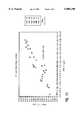
- FIG. 18is a top plan view of an embodiment of overlay target arrays useful in connection with the present invention.
- FIGS. 1-18 of the drawingsin which like numerals refer to like features of the invention.
- Measurement of unresolved pattern arrayshas been accomplished using unmodified optical metrology tools whose primary task is overlay measurement in order to improve accuracy and precision of unresolved patterns metrology.
- the present inventionapplies an optical metrology method to detect the edges of pattern arrays made up of discrete patterns of the type used in image shortening arrays, while the array elements themselves are not resolved by the metrology system.
- the array elementscan be any shape or orientation as long as they are configured so that the element edges at the ends of rows define an array edge.
- FIGS. 1-6A series of different array patterns useful in connection with the method of the present invention are shown in FIGS. 1-6.
- the elementshave a length and a width, and are aligned in rows such that ends of the elements form the edges of the arrays.
- FIG. 1illustrates a pair of array patterns useful in applications where line end shortening is used, as described in the aforementioned incorporated applications.
- the array patternshave elements 120 extending horizontally whose element spacing is equal to the element width, and whose element width is less than the element length. Each element is continuous across the array width, and the element ends form opposite edges of the arrays.
- Each arrayhas a width less than the array length.
- FIG. 2illustrates a pair of array patterns having elements 122 extending vertically whose element spacing is again equal to the element width, and whose element width is again less than the element length. Each element is also continuous across the array width, and the element ends form opposite edges of the arrays. However, each array has a width (equal to the element length) greater than the array length. The array edges are 90° to the direction of the length of elements 122.
- FIG. 3illustrates a pair of array patterns made up of discontinuous, staggered elements 124 extending in vertical rows.
- element spacingis equal to the element width, and element width is less than the element length.
- each element in a vertical row(in the direction of its length) is spaced from adjacent elements by the same spacing as that between rows.
- the rows of elementsare staggered so that the spacing between elements in a row is not aligned perpendicular to the rows, but is at an angle less than 90° thereto.
- the ends of the elements at the ends of the rowsform array edge 124a which is at an angle less than 90° to direction of the row of elements.
- FIG. 4illustrates a pair of array patterns having elements 125 whose element spacing is again equal to the element width, and whose element width is again less than the element length. However, elements 125 extend at an angle of 45° to the array edges. Each element is continuous along its length, and the element ends form opposite edges of the arrays.
- the array width D arrayis 1.414 ⁇ element length.
- FIG. 5illustrates a pair of array patterns made up of discontinuous, elements 126 extending in vertical rows.
- element spacingis equal to the element width, but in this example each element is square so that element width is equal to element length and each element in a vertical row is spaced from adjacent elements by the same spacing as that between rows.
- the elementsare aligned both vertically and horizontally so that the array edges are 90° to the direction of the vertical row of elements 122, but the elements may also be staggered in rows as shown in FIG. 3.
- the elements of an array pattern such as that shown in FIG. 5may be made up of functional features, for example, 0.3 ⁇ m diameter contacts, etched in a substrate, so that it would not be necessary to etch a separate target pattern into the substrate to check bias.
- FIG. 6illustrates a pair of array patterns made up of discontinuous, square elements 128 staggered in overlapping rows. Again, element spacing within a particular vertical row is equal to the element width, but each vertical row overlaps with an adjacent vertical row. The elements are aligned so that the element spacing between adjacent rows is less than 90° to the direction of the vertical row of elements.
- the present inventionis applicable to the control of all types of lithographic patterns, for example, lines, trenches, contacts and the like, where the array edge tracks the edge of individual elements with process variation.
- An important aspect of the present inventionis the ability to modify the resolution of the optical metrology tool by way of wavelength of the light source and/or numerical aperture of the microscope in conjunction with the configuration of the pattern array, such that the individual elements of the array are not resolved and the edges of the array are resolved.
- the present inventionrequires no lower limit on the element dimensions. To achieve optimum measurement precision with smaller element dimensions, the resolution needs to be tuned such that the pitch of the array elements falls just below the inverse of the spatial frequency cutoff of the optical metrology system.
- F cThe spatial frequency cutoff (F c ) of an optical system is determined by its wavelength and numerical aperture, and the degree of coherence of its illumination.
- F cis proportional to NA/wavelength and the minimum resolvable pitch P min is given by: ##EQU2## where: P--the sum of element width and element spacing in the target array
- the measurable array dimension D arraywill track the dimensional variation of the elements.
- the optical measurement of the arrayenables in-line control of the element dimension.
- an optical metrology toolcomprises a light source 101, a beam splitter 103, a lens 105 and an image plane 107.
- the numerical aperture of Light beam 109 emitted from light source 101has a wavelength ⁇ .
- Beam splitter 103comprises a partially transmitting mirror, such that a portion of the light intensity of beams 109 is reflected down as beam 111 through lens 105.
- Below lens 105is a target array 113 (FIG. 8) comprising a plurality of elements 115 of width w and length/separated by spaces (troughs) of width s lithographically printed against a background substrate 100.
- Elements 115can be continuous lines across the width of the array (equal to /), as shown in FIG.
- wis equal to s, although in accordance with the method of the present invention w can also be greater than or less than s.
- the pitch of the elements Pis equal to the sum of w and s.
- the values for w, s, NA, ⁇ and ⁇are such that P is less than or equal to ⁇ / NA (1+ ⁇ )!.
- D arrayas shown equals (5 ⁇ w)+(4 ⁇ s), and is considerably greater than P. While / is greater than D array as seen in FIG. 8, / may also be equal to or less than D array .
- Beams 123form image 125 on image plane 107.
- the width of the imageis D array , i.e., equal to the width of target 113.
- the pitchmay have a fixed value and the light source wavelength, numerical aperature and coherence may be selected, or the light source wavelength may have a fixed value and the pitch, numerical aperature and coherence may be selected, or the numerical aperature may have a fixed value and the light source wavelength and pitch may be selected.
- the targetis always contrasted against the background of the substrate.
- a microscope having control of these parameters(NA, ⁇ , ⁇ ) is useful for measuring unresolved patterns, since the microscope can be tuned so that the array is just barely unresolved. Changing light source wavelength may introduce pattern contrast problems and decreasing a may introduce edge ringing and other less desirable coherence issues.
- the microscope parameter controlledis the numerical aperture value, NA, as may be controlled by a variable diameter pupil or iris.
- a darkfield application of the optical metrology systemwill also be operable.
- other imaging approachesas can be envisioned with desirable asymmetric properties for measuring unresolved patterns.
- confocal microscopescan be constructed with elliptical or rectangular spot shapes (rather than the usual circular spot shape) which can be oriented appropriately to the pattern under test.
- a scatterometerwhich collects light scattered horizontally separately from light scattered vertically may be utilized for any desired array pattern to be measured. Every repeating pattern will have a Fourier spectrum which describes what angles light will scatter from the pattern. By collecting at these known scattering angles, through spatial filters, one can distinguish the areas containing the periodic pattern from those not containing the pattern with high resolution.
- a substrate having lithographically printed contact hole of 300 nm sizehas been controlled using the method of the present invention.
- An array of 300 nm diameter contacts having a 600 nm pitchwas measured through a focus-exposure matrix.
- the array dimension variationas measured on a Biorad Optical Metrology Tool and shown in FIG. 10, correlated to that of the individual contacts, as measured on an Opal SEM and shown in FIG. 9.
- the measurement capabilitywas shown to be a sensitive function of the optical resolution, since improved measurement capability was observed at lower, rather than higher, resolution. Best performance was observed using the red filter to achieve a 575-625 nm light wavelength, a numerical aperture of 0.7 and partial coherence of 0.5, such that individual contacts were unresolved.
- the sensitivity and precision of the measurement technique of the present inventionappears to be equal to or better than that of current SEMs due to the inherent averaging over many elements and the good focus repeatability of the Biorad system.
- the sensitivity to dose/focus variationis illustrated in FIG. 11, which shows a plot of the array dimension versus the SEM critical dimension over the range of conditions used in the measurements shown in FIGS. 9 and 10. The best fit slope is approximately 1, indicating comparable sensitivity.
- the repeatability of the individual optical measurementsis less than 7.5 nm (3 ⁇ ), as compared to SEM repeatability greater than 10 nm (3 ⁇ ).
- Accuracy of the present systemmay be checked by calibration to SEM cross-section and/or AFM profiles. Such calibration is anticipated to be infrequent due to the demonstrable stability of the optical metrology tool.
- the contact hole array used in Example 1places the most severe constraint on the optical resolution because the array pitch is equal along the length and width of the array. Even under this condition the precision of the optical measurement of the array width is superior to the SEM measurement of the individual contact. In instances where the pitch of the array patterns differs in different directions, the metrology optics can be further optimized for the particular pattern being used by using spatial filter techniques.
- One spatial filter methodis the use of a noncircular pupil aperture, e.g., a rectangular or elliptical shape.
- the optical resolutioncan be made low in one direction, so as not to resolve the pattern, and high in another direction, so as to make a sharp measurement.
- Blades 54, 56are movable toward and away from each other in the vertical direction and have inner pupil edges, 55, 57, respectively.
- Blades 58, 60are movable toward and away from each other in the horizontal direction and have inner pupil edges 59, 61, respectively.
- Inner edges 55, 57, 59, 61define the pupil of the microscope objective.
- the array 50consists of a number of lines or elements 52 which have a width w of 350 nm, a length / of 2 microns, and spacing s between elements of 350 nm.
- the width of the arrayequals the length /, i.e., 2 microns.
- the ends of elements 52form the array edges.
- the length of the arrayequals the number of elements, 16, times the element width, 350 nm, plus the number of spaces, 15, times the spacing, 350 nm, or 10.85 microns.
- the edge of the line-shortening patternshows distinctive ripples, due to the individual lines being resolved, which makes more difficult the task of measuring the line length.
- the individual horizontal linesare now completely unresolved.
- the image profile slopeis somewhat degraded, as can be seen by the relatively wide spacing of the contour lines.
- FIG. 16shows contours using a rectangular pupil filter similar to FIG. 13, where the horizontal NA is 0.7 and the vertical NA has been reduced to 0.37, as may be achieved by use of a non-circular pupil.
- test pattern 40any of the array patterns useful in the present invention, for example, test pattern 40, may be printed in conjunction with the desired device pattern on the product wafer 42.
- the elements of the test pattern 40should have a width and pitch smaller than or equal to (corresponding to) that of the most critical feature of the device pattern.
- test pattern 40can contain a plurality of array lines, the minimum width and space of the arrays can be varied to cover a range of dimensions below and above the intended design minimum features or the minimum capability of the lithographic process and tool. At a minimum, at least one array of lines will constitute the test pattern. As shown in FIG.
- test patterns 40can be distributed over any areas not occupied by the product patterns 44 and/or other requisite alignment and measurement patterns.
- similar test patterns of varying line width and patchcan be distributed throughout the image field and wafer.
- FIG. 18An embodiment of an overlay target made up of level specific arrays is depicted in FIG. 18.
- a first target portion on one level of a substrateis shown comprised of arrays 132 and 134 oriented with elements 133, 135, respectively in the X direction (elements lengths parallel to the X-axis) and arrays 140 and 142 oriented with elements 141, 143, respectively in the Y direction (elements lengths parallel to the Y-axis). Element spacing is equal to element width in arrays 132, 134, 140 and 142.
- Opposite arraysare equidistant from target center point 131.
- Array pairscomprise separate targets wherein the nominal distance between facing edges of the array pairs (on the mask or reticle) is a predetermined, selected value.
- array pairs 140, 142also comprise separate targets arranged in a like manner.
- a second target portion printed on another level of a substrateis comprised of arrays 152, 154, 156 and 158 having discrete, square elements 153, 155, 157 and 159, respectively, aligned in rows parallel to the X- and Y- axes. Opposite arrays are equidistant from target center point 151. Element spacing is equal to element width in arrays 152, 154, 156 and 158.
- the image of target arrays 132, 134, 140 and 142is exposed and etched on one level of a substrate and the image of target arrays 152, 154, 156 and 158 is exposed and etched on a a different level the substrate such that the center points 131, 151 of the target portions are coincident and the X and Y orientation of the respective element lengths are preserved.
- the bias and overlay errormay be calculated for the X and Y directions by measurement of distances between edges within an array, or between arrays on the same or different levels. Measurements may be made during processing to check both exposure and development of the desired device pattern and subsequent etching of the pattern into the wafer substrate.
- the target depicted in FIG. 18may also be used as a direct replacement for a conventional box-in-box target employed in the prior art.
Landscapes
- Physics & Mathematics (AREA)
- General Physics & Mathematics (AREA)
- Health & Medical Sciences (AREA)
- Life Sciences & Earth Sciences (AREA)
- Chemical & Material Sciences (AREA)
- Analytical Chemistry (AREA)
- Biochemistry (AREA)
- General Health & Medical Sciences (AREA)
- Immunology (AREA)
- Pathology (AREA)
- Exposure And Positioning Against Photoresist Photosensitive Materials (AREA)
- Length Measuring Devices By Optical Means (AREA)
- Micromachines (AREA)
Abstract
Description
Claims (20)
Priority Applications (5)
| Application Number | Priority Date | Filing Date | Title |
|---|---|---|---|
| US08/643,138US5805290A (en) | 1996-05-02 | 1996-05-02 | Method of optical metrology of unresolved pattern arrays |
| JP10362297AJP3373754B2 (en) | 1996-05-02 | 1997-04-21 | Method of determining bias or overlay error on a substrate |
| US08/919,993US6130750A (en) | 1996-05-02 | 1997-08-28 | Optical metrology tool and method of using same |
| KR1019980034917AKR100276851B1 (en) | 1996-05-02 | 1998-08-27 | Optical metrology tool and method of using same |
| US09/352,296US6317211B1 (en) | 1996-05-02 | 1999-07-12 | Optical metrology tool and method of using same |
Applications Claiming Priority (1)
| Application Number | Priority Date | Filing Date | Title |
|---|---|---|---|
| US08/643,138US5805290A (en) | 1996-05-02 | 1996-05-02 | Method of optical metrology of unresolved pattern arrays |
Related Child Applications (1)
| Application Number | Title | Priority Date | Filing Date |
|---|---|---|---|
| US08/919,993Continuation-In-PartUS6130750A (en) | 1996-05-02 | 1997-08-28 | Optical metrology tool and method of using same |
Publications (1)
| Publication Number | Publication Date |
|---|---|
| US5805290Atrue US5805290A (en) | 1998-09-08 |
Family
ID=24579513
Family Applications (3)
| Application Number | Title | Priority Date | Filing Date |
|---|---|---|---|
| US08/643,138Expired - LifetimeUS5805290A (en) | 1996-05-02 | 1996-05-02 | Method of optical metrology of unresolved pattern arrays |
| US08/919,993Expired - LifetimeUS6130750A (en) | 1996-05-02 | 1997-08-28 | Optical metrology tool and method of using same |
| US09/352,296Expired - Fee RelatedUS6317211B1 (en) | 1996-05-02 | 1999-07-12 | Optical metrology tool and method of using same |
Family Applications After (2)
| Application Number | Title | Priority Date | Filing Date |
|---|---|---|---|
| US08/919,993Expired - LifetimeUS6130750A (en) | 1996-05-02 | 1997-08-28 | Optical metrology tool and method of using same |
| US09/352,296Expired - Fee RelatedUS6317211B1 (en) | 1996-05-02 | 1999-07-12 | Optical metrology tool and method of using same |
Country Status (3)
| Country | Link |
|---|---|
| US (3) | US5805290A (en) |
| JP (1) | JP3373754B2 (en) |
| KR (1) | KR100276851B1 (en) |
Cited By (80)
| Publication number | Priority date | Publication date | Assignee | Title |
|---|---|---|---|---|
| US6064485A (en)* | 1999-06-30 | 2000-05-16 | United Microelectronics Corp. | Method of optical proximity correction |
| US6130750A (en)* | 1996-05-02 | 2000-10-10 | International Business Machines Corporation | Optical metrology tool and method of using same |
| US6191036B1 (en)* | 1999-04-12 | 2001-02-20 | Advanced Micro Devices, Inc. | Use of photoresist focus exposure matrix array as via etch monitor |
| US6429667B1 (en) | 2000-06-19 | 2002-08-06 | International Business Machines Corporation | Electrically testable process window monitor for lithographic processing |
| US6462818B1 (en) | 2000-06-22 | 2002-10-08 | Kla-Tencor Corporation | Overlay alignment mark design |
| US20020158193A1 (en)* | 2001-02-12 | 2002-10-31 | Abdurrahman Sezginer | Overlay alignment metrology using diffraction gratings |
| US6486954B1 (en) | 2000-09-01 | 2002-11-26 | Kla-Tencor Technologies Corporation | Overlay alignment measurement mark |
| US20030015674A1 (en)* | 2001-07-17 | 2003-01-23 | Oliver Broermann | Measuring configuration and method for measuring a critical dimension of at least one feature on a semiconductor wafer |
| US20030058443A1 (en)* | 1998-03-06 | 2003-03-27 | Yiping Xu | Spectroscopic scatterometer system |
| US20030073013A1 (en)* | 2001-08-21 | 2003-04-17 | Michael Hsu | Method for improved lithographic patterning utilizing multiple coherency optimized exposures and high transmission attenuated PSM |
| US6556361B1 (en)* | 1999-03-17 | 2003-04-29 | Rochester Institute Of Technology | Projection imaging system with a non-circular aperture and a method thereof |
| US20030095267A1 (en)* | 2001-11-09 | 2003-05-22 | Mieher Walter Dean | Focus masking structures, focus patterns and measurements thereof |
| US20030129509A1 (en)* | 2002-01-07 | 2003-07-10 | Mitsubishi Denki Kabushiki Kaisha | Evaluation method |
| US6633831B2 (en) | 2000-09-20 | 2003-10-14 | Kla Tencor Technologies | Methods and systems for determining a critical dimension and a thin film characteristic of a specimen |
| US6638671B2 (en) | 2001-10-15 | 2003-10-28 | International Business Machines Corporation | Combined layer-to-layer and within-layer overlay control system |
| US6650135B1 (en) | 2000-06-29 | 2003-11-18 | Motorola, Inc. | Measurement chuck having piezoelectric elements and method |
| US20030223630A1 (en)* | 2002-02-15 | 2003-12-04 | Kla-Tencor Corporation | Overlay metrology and control method |
| WO2003054475A3 (en)* | 2001-12-19 | 2003-12-11 | Kla Tencor Corp | Parametric profiling using optical spectroscopic systems |
| US6673637B2 (en) | 2000-09-20 | 2004-01-06 | Kla-Tencor Technologies | Methods and systems for determining a presence of macro defects and overlay of a specimen |
| US20040017575A1 (en)* | 2002-07-25 | 2004-01-29 | Raghu Balasubramanian | Optimized model and parameter selection for optical metrology |
| US20040017574A1 (en)* | 2002-07-25 | 2004-01-29 | Vi Vuong | Model and parameter selection for optical metrology |
| US6694284B1 (en) | 2000-09-20 | 2004-02-17 | Kla-Tencor Technologies Corp. | Methods and systems for determining at least four properties of a specimen |
| US6699627B2 (en) | 2000-12-08 | 2004-03-02 | Adlai Smith | Reference wafer and process for manufacturing same |
| US6730444B2 (en) | 2001-06-05 | 2004-05-04 | Micron Technology, Inc. | Needle comb reticle pattern for critical dimension and registration measurements using a registration tool and methods for using same |
| US6734971B2 (en)* | 2000-12-08 | 2004-05-11 | Lael Instruments | Method and apparatus for self-referenced wafer stage positional error mapping |
| US20040109165A1 (en)* | 2001-06-15 | 2004-06-10 | Bernard Fay | Automated overlay metrology system |
| US6782337B2 (en) | 2000-09-20 | 2004-08-24 | Kla-Tencor Technologies Corp. | Methods and systems for determining a critical dimension an a presence of defects on a specimen |
| US20040169861A1 (en)* | 2002-12-05 | 2004-09-02 | Kla-Tenor Technologies Corporation | Apparatus and method for detecting overlay errors using scatterometry |
| US20040184030A1 (en)* | 2002-11-12 | 2004-09-23 | Armin Liebchen | Method and apparatus for providing lens aberration compensation by illumination source optimization |
| US6803995B2 (en) | 2001-01-17 | 2004-10-12 | International Business Machines Corporation | Focus control system |
| US20040212796A1 (en)* | 2003-04-25 | 2004-10-28 | Michael Adel | Method and mark for metrology of phase errors on phase shift masks |
| US6812045B1 (en) | 2000-09-20 | 2004-11-02 | Kla-Tencor, Inc. | Methods and systems for determining a characteristic of a specimen prior to, during, or subsequent to ion implantation |
| US20040265707A1 (en)* | 2003-03-31 | 2004-12-30 | Robert Socha | Source and mask optimization |
| US6842237B2 (en) | 2001-12-28 | 2005-01-11 | International Business Machines Corporation | Phase shifted test pattern for monitoring focus and aberrations in optical projection systems |
| US6879400B2 (en) | 2000-12-11 | 2005-04-12 | International Business Machines Corporation | Single tone process window metrology target and method for lithographic processing |
| US6891627B1 (en) | 2000-09-20 | 2005-05-10 | Kla-Tencor Technologies Corp. | Methods and systems for determining a critical dimension and overlay of a specimen |
| US20050105092A1 (en)* | 2003-11-19 | 2005-05-19 | International Business Machines Corporation | Overlay target and measurement method using reference and sub-grids |
| US6919957B2 (en) | 2000-09-20 | 2005-07-19 | Kla-Tencor Technologies Corp. | Methods and systems for determining a critical dimension, a presence of defects, and a thin film characteristic of a specimen |
| US6921916B2 (en) | 2000-08-30 | 2005-07-26 | Kla -Tenocor Technologies Corporation | Overlay marks, methods of overlay mark design and methods of overlay measurements |
| US6949462B1 (en) | 2002-04-04 | 2005-09-27 | Nanometrics Incorporated | Measuring an alignment target with multiple polarization states |
| US6958819B1 (en) | 2002-04-04 | 2005-10-25 | Nanometrics Incorporated | Encoder with an alignment target |
| US6970255B1 (en) | 2003-04-23 | 2005-11-29 | Nanometrics Incorporated | Encoder measurement based on layer thickness |
| US6975398B2 (en) | 2001-10-15 | 2005-12-13 | International Business Machines Corporation | Method for determining semiconductor overlay on groundrule devices |
| US6982793B1 (en) | 2002-04-04 | 2006-01-03 | Nanometrics Incorporated | Method and apparatus for using an alignment target with designed in offset |
| US6992764B1 (en) | 2002-09-30 | 2006-01-31 | Nanometrics Incorporated | Measuring an alignment target with a single polarization state |
| US7046361B1 (en) | 2002-04-04 | 2006-05-16 | Nanometrics Incorporated | Positioning two elements using an alignment target with a designed offset |
| US7061615B1 (en) | 2001-09-20 | 2006-06-13 | Nanometrics Incorporated | Spectroscopically measured overlay target |
| US7106425B1 (en) | 2000-09-20 | 2006-09-12 | Kla-Tencor Technologies Corp. | Methods and systems for determining a presence of defects and a thin film characteristic of a specimen |
| US20060209276A1 (en)* | 2000-12-08 | 2006-09-21 | Smith Adlai H | Method and apparatus for self-referenced wafer stage positional error mapping |
| US7130029B2 (en) | 2000-09-20 | 2006-10-31 | Kla-Tencor Technologies Corp. | Methods and systems for determining an adhesion characteristic and a thickness of a specimen |
| US20060290947A1 (en)* | 2005-06-16 | 2006-12-28 | Timbre Technologies, Inc. | Optical metrology model optimization for repetitive structures |
| US20070041003A1 (en)* | 2005-08-18 | 2007-02-22 | International Business Machines Corporation | Focus blur measurement and control method |
| US20070058169A1 (en)* | 2005-09-13 | 2007-03-15 | International Business Machines Corporation | Multi-layer Alignment and Overlay Target and Measurement Method |
| US7193715B2 (en) | 2002-11-14 | 2007-03-20 | Tokyo Electron Limited | Measurement of overlay using diffraction gratings when overlay exceeds the grating period |
| US20070072091A1 (en)* | 2000-12-08 | 2007-03-29 | Smith Adlai H | Reference wafer and process for manufacturing same |
| US20070108368A1 (en)* | 2002-02-26 | 2007-05-17 | Kla-Tencor Corporation | Focus masking structures, focus patterns and measurements thereof |
| US20080026298A1 (en)* | 2006-07-31 | 2008-01-31 | International Business Machines Corporation | Method to optimize grating test pattern for lithography monitoring and control |
| US7346878B1 (en) | 2003-07-02 | 2008-03-18 | Kla-Tencor Technologies Corporation | Apparatus and methods for providing in-chip microtargets for metrology or inspection |
| US7349090B2 (en) | 2000-09-20 | 2008-03-25 | Kla-Tencor Technologies Corp. | Methods and systems for determining a property of a specimen prior to, during, or subsequent to lithography |
| US20080094639A1 (en)* | 2006-10-24 | 2008-04-24 | Kla-Tencor Technologies Corporation | Waferless recipe optimization |
| US20080174778A1 (en)* | 2007-01-23 | 2008-07-24 | Taiwan Semiconductor Manufacturing Company, Ltd. | Method and System For Optimizing Sub-Nanometer Critical Dimension Using Pitch Offset |
| US20080215275A1 (en)* | 2004-10-26 | 2008-09-04 | Nikon Corporation | Overlay Inspection System |
| US7440105B2 (en) | 2002-12-05 | 2008-10-21 | Kla-Tencor Technologies Corporation | Continuously varying offset mark and methods of determining overlay |
| US20080311344A1 (en)* | 2007-06-13 | 2008-12-18 | Asml Netherlands B.V. | Inspection method and apparatus, lithographic apparatus, lithographic processing cell and device manufacturing method |
| US7508976B1 (en) | 2003-12-29 | 2009-03-24 | Nanometric Incorporated | Local process variation correction for overlay measurement |
| US7515253B2 (en) | 2005-01-12 | 2009-04-07 | Kla-Tencor Technologies Corporation | System for measuring a sample with a layer containing a periodic diffracting structure |
| US7557921B1 (en) | 2005-01-14 | 2009-07-07 | Kla-Tencor Technologies Corporation | Apparatus and methods for optically monitoring the fidelity of patterns produced by photolitographic tools |
| US20090186286A1 (en)* | 2008-01-21 | 2009-07-23 | International Business Machines Corporation | Method To Control Semiconductor Device Overlay Using Post Etch Image Metrology |
| US7608468B1 (en) | 2003-07-02 | 2009-10-27 | Kla-Tencor Technologies, Corp. | Apparatus and methods for determining overlay and uses of same |
| US20110122496A1 (en)* | 2006-06-20 | 2011-05-26 | Asml Netherlands B.V. | Substrate Used in a Method and Apparatus for Angular-Resolved Spectroscopic Lithography Characterization |
| US8138498B2 (en) | 2000-08-30 | 2012-03-20 | Kla-Tencor Technologies Corporation | Apparatus and methods for determining overlay of structures having rotational or mirror symmetry |
| USD690200S1 (en) | 2010-11-02 | 2013-09-24 | The J.M. Smucker Company | Container |
| US9075944B2 (en) | 2008-04-17 | 2015-07-07 | Mentor Graphics Corporation | System and method of predicting problematic areas for lithography in a circuit design |
| US9097989B2 (en) | 2009-01-27 | 2015-08-04 | International Business Machines Corporation | Target and method for mask-to-wafer CD, pattern placement and overlay measurement and control |
| US9182219B1 (en)* | 2013-01-21 | 2015-11-10 | Kla-Tencor Corporation | Overlay measurement based on moire effect between structured illumination and overlay target |
| EP1314198B1 (en)* | 2000-08-30 | 2017-03-08 | KLA-Tencor Corporation | Overlay marks, methods of overlay mark design and methods of overlay measurements |
| US9927718B2 (en) | 2010-08-03 | 2018-03-27 | Kla-Tencor Corporation | Multi-layer overlay metrology target and complimentary overlay metrology measurement systems |
| US10451412B2 (en) | 2016-04-22 | 2019-10-22 | Kla-Tencor Corporation | Apparatus and methods for detecting overlay errors using scatterometry |
| US10890436B2 (en) | 2011-07-19 | 2021-01-12 | Kla Corporation | Overlay targets with orthogonal underlayer dummyfill |
| US11119414B2 (en) | 2013-12-17 | 2021-09-14 | Asml Netherlands B.V. | Yield estimation and control |
Families Citing this family (117)
| Publication number | Priority date | Publication date | Assignee | Title |
|---|---|---|---|---|
| US6578188B1 (en)* | 1997-09-17 | 2003-06-10 | Numerical Technologies, Inc. | Method and apparatus for a network-based mask defect printability analysis system |
| US7107571B2 (en)* | 1997-09-17 | 2006-09-12 | Synopsys, Inc. | Visual analysis and verification system using advanced tools |
| US7093229B2 (en)* | 1997-09-17 | 2006-08-15 | Synopsys, Inc. | System and method for providing defect printability analysis of photolithographic masks with job-based automation |
| US6757645B2 (en) | 1997-09-17 | 2004-06-29 | Numerical Technologies, Inc. | Visual inspection and verification system |
| US7617474B2 (en)* | 1997-09-17 | 2009-11-10 | Synopsys, Inc. | System and method for providing defect printability analysis of photolithographic masks with job-based automation |
| DE19902624A1 (en)* | 1998-01-29 | 1999-09-30 | Leica Microsystems | Optical arrangement for producing a spectral fanning out of a light beam |
| US6094256A (en)* | 1998-09-29 | 2000-07-25 | Nikon Precision Inc. | Method for forming a critical dimension test structure and its use |
| US20020158197A1 (en)* | 1999-01-12 | 2002-10-31 | Applied Materials, Inc | AFM-based lithography metrology tool |
| US6249590B1 (en)* | 1999-02-01 | 2001-06-19 | Eastman Kodak Company | Method for automatically locating image pattern in digital images |
| JP2000267258A (en)* | 1999-03-16 | 2000-09-29 | Nec Corp | Reticle |
| KR100546160B1 (en)* | 1999-04-16 | 2006-01-24 | 주식회사 하이닉스반도체 | Measurement method of sigma value change of optical illuminator |
| KR100702741B1 (en)* | 1999-06-29 | 2007-04-03 | 어플라이드 머티어리얼스, 인코포레이티드 | Integrated Critical Control for Semiconductor Device Manufacturing |
| US6424876B1 (en)* | 1999-07-22 | 2002-07-23 | Advanced Micro Devices, Inc. | Statistical process control system with normalized control charting |
| US6368879B1 (en)* | 1999-09-22 | 2002-04-09 | Advanced Micro Devices, Inc. | Process control with control signal derived from metrology of a repetitive critical dimension feature of a test structure on the work piece |
| US6532428B1 (en)* | 1999-10-07 | 2003-03-11 | Advanced Micro Devices, Inc. | Method and apparatus for automatic calibration of critical dimension metrology tool |
| US20030235936A1 (en)* | 1999-12-16 | 2003-12-25 | Snyder John P. | Schottky barrier CMOS device and method |
| US6949787B2 (en)* | 2001-08-10 | 2005-09-27 | Spinnaker Semiconductor, Inc. | Transistor having high dielectric constant gate insulating layer and source and drain forming Schottky contact with substrate |
| US6337217B1 (en)* | 2000-02-14 | 2002-01-08 | Advanced Micro Devices, Inc. | Method and apparatus for improved focus in optical processing |
| JP2003532306A (en)* | 2000-05-04 | 2003-10-28 | ケーエルエー・テンコール・テクノロジーズ・コーポレーション | Method and system for lithographic process control |
| US6710876B1 (en)* | 2000-08-14 | 2004-03-23 | Kla-Tencor Technologies Corporation | Metrology system using optical phase |
| KR100811964B1 (en)* | 2000-09-28 | 2008-03-10 | 동경 엘렉트론 주식회사 | Resist pattern forming apparatus and method thereof |
| US6750968B2 (en)* | 2000-10-03 | 2004-06-15 | Accent Optical Technologies, Inc. | Differential numerical aperture methods and device |
| US7009704B1 (en)* | 2000-10-26 | 2006-03-07 | Kla-Tencor Technologies Corporation | Overlay error detection |
| KR100383258B1 (en)* | 2000-11-09 | 2003-05-09 | 삼성전자주식회사 | measurement error detecting method of measurement apparatus using scanning electron microscope |
| US6346426B1 (en)* | 2000-11-17 | 2002-02-12 | Advanced Micro Devices, Inc. | Method and apparatus for characterizing semiconductor device performance variations based on independent critical dimension measurements |
| US6625497B2 (en)* | 2000-11-20 | 2003-09-23 | Applied Materials Inc. | Semiconductor processing module with integrated feedback/feed forward metrology |
| IL140179A (en)* | 2000-12-07 | 2004-09-27 | Nova Measuring Instr Ltd | Method and system for measuring in patterned structures |
| TW519746B (en)* | 2001-01-26 | 2003-02-01 | Timbre Tech Inc | System and method for characterizing macro-grating test patterns in advanced lithography and etch processes |
| US6898037B2 (en) | 2001-02-20 | 2005-05-24 | Seagate Technology Llc | Optical equipment assemblies and techniques |
| US6620563B2 (en)* | 2001-03-08 | 2003-09-16 | Motorola, Inc. | Lithography method for forming semiconductor devices on a wafer utilizing atomic force microscopy |
| US6925202B2 (en)* | 2001-03-20 | 2005-08-02 | Synopsys, Inc. | System and method of providing mask quality control |
| US6873720B2 (en)* | 2001-03-20 | 2005-03-29 | Synopsys, Inc. | System and method of providing mask defect printability analysis |
| US20030002043A1 (en) | 2001-04-10 | 2003-01-02 | Kla-Tencor Corporation | Periodic patterns and technique to control misalignment |
| US6956659B2 (en)* | 2001-05-22 | 2005-10-18 | Nikon Precision Inc. | Measurement of critical dimensions of etched features |
| US6560766B2 (en) | 2001-07-26 | 2003-05-06 | Numerical Technologies, Inc. | Method and apparatus for analyzing a layout using an instance-based representation |
| US6721928B2 (en) | 2001-07-26 | 2004-04-13 | Numerical Technologies, Inc. | Verification utilizing instance-based hierarchy management |
| US20060079059A1 (en)* | 2001-08-10 | 2006-04-13 | Snyder John P | Transistor having high dielectric constant gate insulating layer and source and drain forming schottky contact with substrate |
| US7014955B2 (en)* | 2001-08-28 | 2006-03-21 | Synopsys, Inc. | System and method for indentifying dummy features on a mask layer |
| WO2003025497A1 (en)* | 2001-09-21 | 2003-03-27 | Kmac | Apparatus for measuring thickness profile and refractive index distribution of multiple layers of thin films by means of two-dimensional reflectometry and method of measuring the same |
| KR100490325B1 (en)* | 2001-09-21 | 2005-05-17 | 케이맥(주) | Apparatus for measuring characteristics of thin film by means of two-dimensional detector and method of measuring the same |
| US6894790B2 (en)* | 2001-11-13 | 2005-05-17 | Hitachi High-Technologies Corporation | Micropattern shape measuring system and method |
| US6976240B2 (en) | 2001-11-14 | 2005-12-13 | Synopsys Inc. | Simulation using design geometry information |
| US6716559B2 (en) | 2001-12-13 | 2004-04-06 | International Business Machines Corporation | Method and system for determining overlay tolerance |
| US7050162B2 (en)* | 2002-01-16 | 2006-05-23 | Therma-Wave, Inc. | Optical metrology tool having improved contrast |
| JP4011353B2 (en)* | 2002-01-31 | 2007-11-21 | 沖電気工業株式会社 | Resist pattern for alignment measurement |
| US6870951B2 (en)* | 2002-02-13 | 2005-03-22 | Numerical Technologies, Inc. | Method and apparatus to facilitate auto-alignment of images for defect inspection and defect analysis |
| US6778275B2 (en)* | 2002-02-20 | 2004-08-17 | Micron Technology, Inc. | Aberration mark and method for estimating overlay error and optical aberrations |
| US20030160163A1 (en)* | 2002-02-25 | 2003-08-28 | Alan Wong | Optical metrology target design for simultaneous measurement of multiple periodic structures |
| US7136796B2 (en)* | 2002-02-28 | 2006-11-14 | Timbre Technologies, Inc. | Generation and use of integrated circuit profile-based simulation information |
| IL148485A (en)* | 2002-03-04 | 2008-07-08 | Nova Measuring Instr Ltd | Optical measurement of patterned structure parameters |
| JP3953355B2 (en)* | 2002-04-12 | 2007-08-08 | Necエレクトロニクス株式会社 | Image processing alignment method and semiconductor device manufacturing method |
| US6974653B2 (en)* | 2002-04-19 | 2005-12-13 | Nikon Precision Inc. | Methods for critical dimension and focus mapping using critical dimension test marks |
| US6974737B2 (en)* | 2002-05-16 | 2005-12-13 | Spinnaker Semiconductor, Inc. | Schottky barrier CMOS fabrication method |
| DE10224164B4 (en)* | 2002-05-31 | 2007-05-10 | Advanced Micro Devices, Inc., Sunnyvale | A two-dimensional structure for determining a superposition accuracy by means of scattering measurement |
| US6775015B2 (en)* | 2002-06-18 | 2004-08-10 | Timbre Technologies, Inc. | Optical metrology of single features |
| US6800403B2 (en)* | 2002-06-18 | 2004-10-05 | Koninklijke Philips Electronics N.V. | Techniques to characterize iso-dense effects for microdevice manufacture |
| US7046376B2 (en)* | 2002-07-05 | 2006-05-16 | Therma-Wave, Inc. | Overlay targets with isolated, critical-dimension features and apparatus to measure overlay |
| US6807662B2 (en)* | 2002-07-09 | 2004-10-19 | Mentor Graphics Corporation | Performance of integrated circuit components via a multiple exposure technique |
| EP1573366B1 (en) | 2002-08-24 | 2016-11-09 | Chime Ball Technology Co., Ltd. | Continuous direct-write optical lithography |
| US7043071B2 (en)* | 2002-09-13 | 2006-05-09 | Synopsys, Inc. | Soft defect printability simulation and analysis for masks |
| JP4302965B2 (en)* | 2002-11-01 | 2009-07-29 | 株式会社日立ハイテクノロジーズ | Semiconductor device manufacturing method and manufacturing system thereof |
| US7457736B2 (en)* | 2002-11-21 | 2008-11-25 | Synopsys, Inc. | Automated creation of metrology recipes |
| JP3884371B2 (en)* | 2002-11-26 | 2007-02-21 | 株式会社東芝 | Reticle, exposure monitoring method, exposure method, and semiconductor device manufacturing method |
| JP4272624B2 (en)* | 2002-12-20 | 2009-06-03 | インターナショナル・ビジネス・マシーンズ・コーポレーション | Evaluation and optimization for measuring devices |
| US6934929B2 (en)* | 2003-01-13 | 2005-08-23 | Lsi Logic Corporation | Method for improving OPC modeling |
| US6869739B1 (en) | 2003-01-28 | 2005-03-22 | International Business Machines Corporation | Integrated lithographic print and detection model for optical CD |
| JP4101076B2 (en)* | 2003-02-06 | 2008-06-11 | キヤノン株式会社 | Position detection method and apparatus |
| US7119893B2 (en)* | 2003-04-10 | 2006-10-10 | Accent Optical Technologies, Inc. | Determination of center of focus by parameter variability analysis |
| WO2005001577A1 (en)* | 2003-06-11 | 2005-01-06 | Therma-Wave, Inc. | System and method for optical mertology of semiconductor wafers |
| JP3828552B2 (en)* | 2003-06-23 | 2006-10-04 | 株式会社東芝 | Dimension measurement method, dimension measurement system, and dimension measurement program |
| DE10335565A1 (en)* | 2003-07-31 | 2005-05-19 | Infineon Technologies Ag | Method for checking periodic structures on lithographic masks |
| US7030506B2 (en)* | 2003-10-15 | 2006-04-18 | Infineon Technologies, Ag | Mask and method for using the mask in lithographic processing |
| US20050097764A1 (en)* | 2003-11-10 | 2005-05-12 | Kim Su H. | Enhanced visibility of overlay measurement marks |
| US6967709B2 (en)* | 2003-11-26 | 2005-11-22 | International Business Machines Corporation | Overlay and CD process window structure |
| ATE476687T1 (en) | 2003-12-19 | 2010-08-15 | Ibm | DIFFERENTIAL METROLOGY FOR CRITICAL DIMENSIONS AND SUPERPOSITION |
| US7499600B2 (en)* | 2004-05-25 | 2009-03-03 | Nokia Corporation | Method for characterizing a digital imaging system |
| US7369697B2 (en)* | 2004-06-17 | 2008-05-06 | Intel Corporation | Process variable of interest monitoring and control |
| US7463367B2 (en)* | 2004-07-13 | 2008-12-09 | Micron Technology, Inc. | Estimating overlay error and optical aberrations |
| US7361941B1 (en)* | 2004-12-21 | 2008-04-22 | Kla-Tencor Technologies Corporation | Calibration standards and methods |
| US7408642B1 (en) | 2006-02-17 | 2008-08-05 | Kla-Tencor Technologies Corporation | Registration target design for managing both reticle grid error and wafer overlay |
| US7925486B2 (en)* | 2006-03-14 | 2011-04-12 | Kla-Tencor Technologies Corp. | Computer-implemented methods, carrier media, and systems for creating a metrology target structure design for a reticle layout |
| JP4993934B2 (en)* | 2006-03-31 | 2012-08-08 | Hoya株式会社 | Pattern defect inspection method, photomask manufacturing method, and display device substrate manufacturing method |
| US7446888B2 (en)* | 2006-05-22 | 2008-11-04 | Tokyo Electron Limited | Matching optical metrology tools using diffraction signals |
| US7446887B2 (en)* | 2006-05-22 | 2008-11-04 | Tokyo Electron Limited | Matching optical metrology tools using hypothetical profiles |
| US7573584B2 (en)* | 2006-09-25 | 2009-08-11 | Asml Netherlands B.V. | Method and apparatus for angular-resolved spectroscopic lithography characterization |
| US7710572B2 (en)* | 2006-11-30 | 2010-05-04 | Asml Netherlands B.V. | Inspection method and apparatus, lithographic apparatus, lithographic processing cell and device manufacturing method |
| US8237914B2 (en)* | 2006-12-01 | 2012-08-07 | Asml Netherlands B.V. | Process, apparatus, and device for determining intra-field correction to correct overlay errors between overlapping patterns |
| US8248579B2 (en)* | 2006-12-01 | 2012-08-21 | Asml Netherlands B.V. | Lithographic apparatus, device manufacturing method and device for correcting overlay errors between overlapping patterns |
| US7580131B2 (en)* | 2007-04-17 | 2009-08-25 | Asml Netherlands B.V. | Angularly resolved scatterometer and inspection method |
| US8175831B2 (en) | 2007-04-23 | 2012-05-08 | Kla-Tencor Corp. | Methods and systems for creating or performing a dynamic sampling scheme for a process during which measurements are performed on wafers |
| US7873504B1 (en) | 2007-05-07 | 2011-01-18 | Kla-Tencor Technologies Corp. | Computer-implemented methods, carrier media, and systems for creating a metrology target structure design for a reticle layout |
| US7855844B2 (en) | 2007-05-17 | 2010-12-21 | Mitutoyo Corporation | Objective lens and optical measuring device |
| WO2008151083A1 (en) | 2007-05-30 | 2008-12-11 | Kla-Tencor Corporation | Feedforward/feedback litho process control of stress and overlay |
| GB2451442B (en)* | 2007-07-30 | 2013-03-06 | Lein Applied Diagnostics Ltd | Optical measurement apparatus and method therefor |
| NL1036245A1 (en)* | 2007-12-17 | 2009-06-18 | Asml Netherlands Bv | Diffraction based overlay metrology tool and method or diffraction based overlay metrology. |
| NL1036647A1 (en)* | 2008-04-16 | 2009-10-19 | Asml Netherlands Bv | A method of measuring a lithographic projection apparatus. |
| EP2131243B1 (en)* | 2008-06-02 | 2015-07-01 | ASML Netherlands B.V. | Lithographic apparatus and method for calibrating a stage position |
| KR101071468B1 (en)* | 2009-01-07 | 2011-10-10 | 포항공과대학교 산학협력단 | Apparatus and method for diagnosing beam using interference effect |
| US8214771B2 (en)* | 2009-01-08 | 2012-07-03 | Kla-Tencor Corporation | Scatterometry metrology target design optimization |
| JP2013500597A (en)* | 2009-07-30 | 2013-01-07 | エーエスエムエル ネザーランズ ビー.ブイ. | Inspection method for lithography |
| KR101138647B1 (en)* | 2009-10-08 | 2012-04-24 | 엘아이지에이디피 주식회사 | High speed substrate inspection apparatus and method using the same |
| WO2012022584A1 (en)* | 2010-08-18 | 2012-02-23 | Asml Netherlands B.V. | Substrate for use in metrology, metrology method and device manufacturing method |
| EP2458441B1 (en)* | 2010-11-30 | 2022-01-19 | ASML Netherlands BV | Measuring method, apparatus and substrate |
| CN102969300B (en)* | 2011-09-01 | 2016-01-20 | 上海华力微电子有限公司 | Alignment precision test pattern and using method thereof |
| CN102446902B (en)* | 2011-09-08 | 2015-06-17 | 上海华力微电子有限公司 | Graphic structure integrating dimensional measurement and overlay accuracy detection and method thereof |
| US9588441B2 (en) | 2012-05-18 | 2017-03-07 | Kla-Tencor Corporation | Method and device for using substrate geometry to determine optimum substrate analysis sampling |
| CN102723294B (en)* | 2012-06-20 | 2015-04-22 | 上海华力微电子有限公司 | Method for detecting registration between contact hole and polycrystalline silicon gate |
| KR101609652B1 (en) | 2012-07-10 | 2016-04-06 | 에이에스엠엘 네델란즈 비.브이. | Lithographic cluster system, method for calibrating a positioning device of a lithographic apparatus |
| US9093458B2 (en) | 2012-09-06 | 2015-07-28 | Kla-Tencor Corporation | Device correlated metrology (DCM) for OVL with embedded SEM structure overlay targets |
| JP6061619B2 (en)* | 2012-10-30 | 2017-01-18 | オリンパス株式会社 | Microscope system |
| CN103389041B (en)* | 2013-07-30 | 2016-05-18 | 中节能太阳能科技(镇江)有限公司 | A kind of method of measuring grid line width |
| KR102136671B1 (en)* | 2013-09-06 | 2020-07-22 | 삼성전자주식회사 | Method of detecting a defect of a substrate and apparatus for performing the same |
| DE102016107900B4 (en)* | 2016-04-28 | 2020-10-08 | Carl Zeiss Industrielle Messtechnik Gmbh | Method and device for determining the edge of a measurement object in optical measurement technology |
| US10429271B2 (en)* | 2016-07-01 | 2019-10-01 | Microsoft Technology Licensing, Llc | Camera testing using reverse projection |
| EP3293574A1 (en) | 2016-09-09 | 2018-03-14 | ASML Netherlands B.V. | Metrology method, apparatus and computer program |
| US11346657B2 (en)* | 2020-05-22 | 2022-05-31 | Kla Corporation | Measurement modes for overlay |
| US20210375651A1 (en)* | 2020-05-28 | 2021-12-02 | Kla Corporation | Fleet Matching Of Semiconductor Metrology Tools Without Dedicated Quality Control Wafers |
Citations (11)
| Publication number | Priority date | Publication date | Assignee | Title |
|---|---|---|---|---|
| GB214920A (en)* | 1923-11-07 | 1924-05-01 | Wallace Griffiths | Improvements in and relating to packing for cigars, cigarettes, and tobacco in cartridge form |
| JPS5760206A (en)* | 1980-09-30 | 1982-04-12 | Fujitsu Ltd | Measuring method for length |
| US4529314A (en)* | 1980-04-18 | 1985-07-16 | Harris Corporation | Method of measuring misalignment between levels on a substrate |
| US4568189A (en)* | 1983-09-26 | 1986-02-04 | The United States Of America As Represented By The Secretary Of The Navy | Apparatus and method for aligning a mask and wafer in the fabrication of integrated circuits |
| US4659936A (en)* | 1985-03-22 | 1987-04-21 | Dainippon Screen Mfg. Co., Ltd. | Line width measuring device and method |
| US4820055A (en)* | 1985-08-26 | 1989-04-11 | Siemens Aktiengesellschaft | Apparatus for adjusting a mask with at least one adjustment mark relative to a semi-conductor wafer provided with at least one lattice structure |
| US5103104A (en)* | 1989-12-21 | 1992-04-07 | French State, Minister Of Post, Telecommunications And Space | Process for measuring the dimensions of a spacer |
| US5216257A (en)* | 1990-07-09 | 1993-06-01 | Brueck Steven R J | Method and apparatus for alignment and overlay of submicron lithographic features |
| US5262258A (en)* | 1990-06-12 | 1993-11-16 | Nec Corporation | Process of manufacturing semiconductor devices |
| US5309198A (en)* | 1992-02-25 | 1994-05-03 | Nikon Corporation | Light exposure system |
| US5402224A (en)* | 1992-09-25 | 1995-03-28 | Nikon Corporation | Distortion inspecting method for projection optical system |
Family Cites Families (22)
| Publication number | Priority date | Publication date | Assignee | Title |
|---|---|---|---|---|
| NL6804512A (en)* | 1968-03-30 | 1969-10-02 | ||
| JPS5972728A (en)* | 1982-10-20 | 1984-04-24 | Canon Inc | automatic alignment device |
| US4555798A (en)* | 1983-06-20 | 1985-11-26 | Kla Instruments Corporation | Automatic system and method for inspecting hole quality |
| JPS6050751A (en) | 1983-08-31 | 1985-03-20 | Victor Co Of Japan Ltd | Measuring and checking device of circuit substrate |
| US4631416A (en)* | 1983-12-19 | 1986-12-23 | Hewlett-Packard Company | Wafer/mask alignment system using diffraction gratings |
| US4596037A (en)* | 1984-03-09 | 1986-06-17 | International Business Machines Corporation | Video measuring system for defining location orthogonally |
| US4853967A (en)* | 1984-06-29 | 1989-08-01 | International Business Machines Corporation | Method for automatic optical inspection analysis of integrated circuits |
| JPS6139021A (en)* | 1984-07-31 | 1986-02-25 | Canon Inc | Optical system using variable filter |
| DE3587582D1 (en)* | 1985-03-14 | 1993-10-21 | Beltronics Inc | Device and method for automatically inspecting objects and for identifying or recognizing known and unknown parts thereof, including errors and the like. |
| JPS62247478A (en)* | 1986-04-21 | 1987-10-28 | Hitachi Ltd | Pattern inspection instrument |
| US4783826A (en)* | 1986-08-18 | 1988-11-08 | The Gerber Scientific Company, Inc. | Pattern inspection system |
| JPH01111281A (en)* | 1987-10-23 | 1989-04-27 | Matsushita Electric Ind Co Ltd | Parts recognizing method |
| US4908656A (en)* | 1988-01-21 | 1990-03-13 | Nikon Corporation | Method of dimension measurement for a pattern formed by exposure apparatus, and method for setting exposure conditions and for inspecting exposure precision |
| US5272763A (en)* | 1990-03-02 | 1993-12-21 | Matsushita Electric Industrial Co., Ltd. | Apparatus for inspecting wiring pattern formed on a board |
| JP2712772B2 (en)* | 1990-07-05 | 1998-02-16 | 株式会社ニコン | Pattern position measuring method and apparatus |
| US5119436A (en)* | 1990-09-24 | 1992-06-02 | Kulicke And Soffa Industries, Inc | Method of centering bond positions |
| US5418613A (en)* | 1990-11-20 | 1995-05-23 | Canon Kabushiki Kaisha | Method and apparatus for detecting the position of a substrate having first and second patterns of different sizes |
| US5483345A (en)* | 1994-09-06 | 1996-01-09 | Mrs Technology, Inc. | Alignment system for use in lithography utilizing a spherical reflector having a centered etched-on projection object |
| US5629772A (en)* | 1994-12-20 | 1997-05-13 | International Business Machines Corporation | Monitoring of minimum features on a substrate |
| US5754299A (en)* | 1995-01-13 | 1998-05-19 | Nikon Corporation | Inspection apparatus and method for optical system, exposure apparatus provided with the inspection apparatus, and alignment apparatus and optical system thereof applicable to the exposure apparatus |
| US5706091A (en)* | 1995-04-28 | 1998-01-06 | Nikon Corporation | Apparatus for detecting a mark pattern on a substrate |
| US5805290A (en)* | 1996-05-02 | 1998-09-08 | International Business Machines Corporation | Method of optical metrology of unresolved pattern arrays |
- 1996
- 1996-05-02USUS08/643,138patent/US5805290A/ennot_activeExpired - Lifetime
- 1997
- 1997-04-21JPJP10362297Apatent/JP3373754B2/ennot_activeExpired - Fee Related
- 1997-08-28USUS08/919,993patent/US6130750A/ennot_activeExpired - Lifetime
- 1998
- 1998-08-27KRKR1019980034917Apatent/KR100276851B1/ennot_activeExpired - Fee Related
- 1999
- 1999-07-12USUS09/352,296patent/US6317211B1/ennot_activeExpired - Fee Related
Patent Citations (11)
| Publication number | Priority date | Publication date | Assignee | Title |
|---|---|---|---|---|
| GB214920A (en)* | 1923-11-07 | 1924-05-01 | Wallace Griffiths | Improvements in and relating to packing for cigars, cigarettes, and tobacco in cartridge form |
| US4529314A (en)* | 1980-04-18 | 1985-07-16 | Harris Corporation | Method of measuring misalignment between levels on a substrate |
| JPS5760206A (en)* | 1980-09-30 | 1982-04-12 | Fujitsu Ltd | Measuring method for length |
| US4568189A (en)* | 1983-09-26 | 1986-02-04 | The United States Of America As Represented By The Secretary Of The Navy | Apparatus and method for aligning a mask and wafer in the fabrication of integrated circuits |
| US4659936A (en)* | 1985-03-22 | 1987-04-21 | Dainippon Screen Mfg. Co., Ltd. | Line width measuring device and method |
| US4820055A (en)* | 1985-08-26 | 1989-04-11 | Siemens Aktiengesellschaft | Apparatus for adjusting a mask with at least one adjustment mark relative to a semi-conductor wafer provided with at least one lattice structure |
| US5103104A (en)* | 1989-12-21 | 1992-04-07 | French State, Minister Of Post, Telecommunications And Space | Process for measuring the dimensions of a spacer |
| US5262258A (en)* | 1990-06-12 | 1993-11-16 | Nec Corporation | Process of manufacturing semiconductor devices |
| US5216257A (en)* | 1990-07-09 | 1993-06-01 | Brueck Steven R J | Method and apparatus for alignment and overlay of submicron lithographic features |
| US5309198A (en)* | 1992-02-25 | 1994-05-03 | Nikon Corporation | Light exposure system |
| US5402224A (en)* | 1992-09-25 | 1995-03-28 | Nikon Corporation | Distortion inspecting method for projection optical system |
Cited By (209)
| Publication number | Priority date | Publication date | Assignee | Title |
|---|---|---|---|---|
| US6130750A (en)* | 1996-05-02 | 2000-10-10 | International Business Machines Corporation | Optical metrology tool and method of using same |
| US6317211B1 (en) | 1996-05-02 | 2001-11-13 | International Business Machines Corporation | Optical metrology tool and method of using same |
| US7898661B2 (en) | 1998-03-06 | 2011-03-01 | Kla-Tencor Corporation | Spectroscopic scatterometer system |
| US7173699B2 (en) | 1998-03-06 | 2007-02-06 | Kla-Tencor Technologies Corporation | Spectroscopic scatterometer system |
| US20030058443A1 (en)* | 1998-03-06 | 2003-03-27 | Yiping Xu | Spectroscopic scatterometer system |
| US7859659B2 (en) | 1998-03-06 | 2010-12-28 | Kla-Tencor Corporation | Spectroscopic scatterometer system |
| US6556361B1 (en)* | 1999-03-17 | 2003-04-29 | Rochester Institute Of Technology | Projection imaging system with a non-circular aperture and a method thereof |
| US6191036B1 (en)* | 1999-04-12 | 2001-02-20 | Advanced Micro Devices, Inc. | Use of photoresist focus exposure matrix array as via etch monitor |
| US6064485A (en)* | 1999-06-30 | 2000-05-16 | United Microelectronics Corp. | Method of optical proximity correction |
| US6087049A (en)* | 1999-06-30 | 2000-07-11 | United Microelectronics Corp. | Mixed mode photomask for optical proximity correction in a lithographic process |
| US6429667B1 (en) | 2000-06-19 | 2002-08-06 | International Business Machines Corporation | Electrically testable process window monitor for lithographic processing |
| US20050174574A1 (en)* | 2000-06-22 | 2005-08-11 | Kla-Tencor Corporation | Overlay alignment mark design |
| US6894783B2 (en) | 2000-06-22 | 2005-05-17 | Kla-Tencor Corporation | Overlay alignment mark design |
| US6462818B1 (en) | 2000-06-22 | 2002-10-08 | Kla-Tencor Corporation | Overlay alignment mark design |
| US7102749B2 (en) | 2000-06-22 | 2006-09-05 | Kla-Tencor | Overlay alignment mark design |
| US6580505B1 (en) | 2000-06-22 | 2003-06-17 | Kla-Tencor Corporation | Overlay alignment mark design |
| US6650135B1 (en) | 2000-06-29 | 2003-11-18 | Motorola, Inc. | Measurement chuck having piezoelectric elements and method |
| US7274814B2 (en) | 2000-08-30 | 2007-09-25 | Kla-Tencor Corporation | Overlay marks, methods of overlay mark design and methods of overlay measurements |
| US6985618B2 (en) | 2000-08-30 | 2006-01-10 | Kla-Tencor Technologies Corporation | Overlay marks, methods of overlay mark design and methods of overlay measurements |
| US20060204073A1 (en)* | 2000-08-30 | 2006-09-14 | Kla-Tencor Corporation | Overlay marks, methods of overlay mark design and methods of overlay measurements |
| US7181057B2 (en) | 2000-08-30 | 2007-02-20 | Kla-Tencor Technologies Corporation | Overlay marks, methods of overlay mark design and methods of overlay measurements |
| US7355291B2 (en) | 2000-08-30 | 2008-04-08 | Kla-Tencor Technologies Corporation | Overlay marks, methods of overlay mark design and methods of overlay measurements |
| US20060177120A1 (en)* | 2000-08-30 | 2006-08-10 | Kla-Tencor Corporation | Overlay marks, methods of overlay mark design and methods of overlay measurements |
| US20090291513A1 (en)* | 2000-08-30 | 2009-11-26 | Kla-Tencor Corporation | Overlay marks, methods of overlay mark design and methods of overlay measurements |
| US9702693B2 (en) | 2000-08-30 | 2017-07-11 | Kla-Tencor Corporation | Apparatus for measuring overlay errors |
| EP1314198B1 (en)* | 2000-08-30 | 2017-03-08 | KLA-Tencor Corporation | Overlay marks, methods of overlay mark design and methods of overlay measurements |
| US7068833B1 (en) | 2000-08-30 | 2006-06-27 | Kla-Tencor Corporation | Overlay marks, methods of overlay mark design and methods of overlay measurements |
| US20060039595A1 (en)* | 2000-08-30 | 2006-02-23 | Kla-Tencor Technologies Corporation | Overlay marks, methods of overlay mark design and methods of overlay measurements |
| US7177457B2 (en) | 2000-08-30 | 2007-02-13 | Kla-Tencor Corporation | Overlay marks, methods of overlay mark design and methods of overlay measurements |
| US9347879B2 (en) | 2000-08-30 | 2016-05-24 | Kla-Tencor Corporation | Apparatus and methods for detecting overlay errors using scatterometry |
| US20080023855A1 (en)* | 2000-08-30 | 2008-01-31 | Kla-Tencor Corporation | Overlay marks, methods of overlay mark design and methods of overlay measurements |
| US7879627B2 (en) | 2000-08-30 | 2011-02-01 | Kla-Tencor Technologies Corporation | Overlay marks and methods of manufacturing such marks |
| US8330281B2 (en) | 2000-08-30 | 2012-12-11 | Kla-Tencor Technologies Corporation | Overlay marks, methods of overlay mark design and methods of overlay measurements |
| US8138498B2 (en) | 2000-08-30 | 2012-03-20 | Kla-Tencor Technologies Corporation | Apparatus and methods for determining overlay of structures having rotational or mirror symmetry |
| US7317824B2 (en) | 2000-08-30 | 2008-01-08 | Kla-Tencor Technologies Corporation | Overlay marks, methods of overlay mark design and methods of overlay measurements |
| US6921916B2 (en) | 2000-08-30 | 2005-07-26 | Kla -Tenocor Technologies Corporation | Overlay marks, methods of overlay mark design and methods of overlay measurements |
| US9182680B2 (en) | 2000-08-30 | 2015-11-10 | Kla-Tencor Corporation | Apparatus and methods for determining overlay of structures having rotational or mirror symmetry |
| USRE45245E1 (en) | 2000-08-30 | 2014-11-18 | Kla-Tencor Corporation | Apparatus and methods for determining overlay of structures having rotational or mirror symmetry |
| US6486954B1 (en) | 2000-09-01 | 2002-11-26 | Kla-Tencor Technologies Corporation | Overlay alignment measurement mark |
| US6917419B2 (en) | 2000-09-20 | 2005-07-12 | Kla-Tencor Technologies Corp. | Methods and systems for determining flatness, a presence of defects, and a thin film characteristic of a specimen |
| US6950196B2 (en) | 2000-09-20 | 2005-09-27 | Kla-Tencor Technologies Corp. | Methods and systems for determining a thickness of a structure on a specimen and at least one additional property of the specimen |
| US6812045B1 (en) | 2000-09-20 | 2004-11-02 | Kla-Tencor, Inc. | Methods and systems for determining a characteristic of a specimen prior to, during, or subsequent to ion implantation |
| US7349090B2 (en) | 2000-09-20 | 2008-03-25 | Kla-Tencor Technologies Corp. | Methods and systems for determining a property of a specimen prior to, during, or subsequent to lithography |
| US6818459B2 (en) | 2000-09-20 | 2004-11-16 | Kla-Tencor Technologies Corp. | Methods and systems for determining a presence of macro defects and overlay of a specimen |
| US6829559B2 (en) | 2000-09-20 | 2004-12-07 | K.L.A.-Tencor Technologies | Methods and systems for determining a presence of macro and micro defects on a specimen |
| US6806951B2 (en) | 2000-09-20 | 2004-10-19 | Kla-Tencor Technologies Corp. | Methods and systems for determining at least one characteristic of defects on at least two sides of a specimen |
| US7196782B2 (en) | 2000-09-20 | 2007-03-27 | Kla-Tencor Technologies Corp. | Methods and systems for determining a thin film characteristic and an electrical property of a specimen |
| US7460981B2 (en) | 2000-09-20 | 2008-12-02 | Kla-Tencor Technologies Corp. | Methods and systems for determining a presence of macro and micro defects on a specimen |
| US6633831B2 (en) | 2000-09-20 | 2003-10-14 | Kla Tencor Technologies | Methods and systems for determining a critical dimension and a thin film characteristic of a specimen |
| US7139083B2 (en) | 2000-09-20 | 2006-11-21 | Kla-Tencor Technologies Corp. | Methods and systems for determining a composition and a thickness of a specimen |
| US6891610B2 (en) | 2000-09-20 | 2005-05-10 | Kla-Tencor Technologies Corp. | Methods and systems for determining an implant characteristic and a presence of defects on a specimen |
| US6891627B1 (en) | 2000-09-20 | 2005-05-10 | Kla-Tencor Technologies Corp. | Methods and systems for determining a critical dimension and overlay of a specimen |
| US7130029B2 (en) | 2000-09-20 | 2006-10-31 | Kla-Tencor Technologies Corp. | Methods and systems for determining an adhesion characteristic and a thickness of a specimen |
| US8179530B2 (en) | 2000-09-20 | 2012-05-15 | Kla-Tencor Technologies Corp. | Methods and systems for determining a critical dimension and overlay of a specimen |
| US7106425B1 (en) | 2000-09-20 | 2006-09-12 | Kla-Tencor Technologies Corp. | Methods and systems for determining a presence of defects and a thin film characteristic of a specimen |
| US6917433B2 (en) | 2000-09-20 | 2005-07-12 | Kla-Tencor Technologies Corp. | Methods and systems for determining a property of a specimen prior to, during, or subsequent to an etch process |
| US6673637B2 (en) | 2000-09-20 | 2004-01-06 | Kla-Tencor Technologies | Methods and systems for determining a presence of macro defects and overlay of a specimen |
| US6919957B2 (en) | 2000-09-20 | 2005-07-19 | Kla-Tencor Technologies Corp. | Methods and systems for determining a critical dimension, a presence of defects, and a thin film characteristic of a specimen |
| US6782337B2 (en) | 2000-09-20 | 2004-08-24 | Kla-Tencor Technologies Corp. | Methods and systems for determining a critical dimension an a presence of defects on a specimen |
| US6694284B1 (en) | 2000-09-20 | 2004-02-17 | Kla-Tencor Technologies Corp. | Methods and systems for determining at least four properties of a specimen |
| US7751046B2 (en) | 2000-09-20 | 2010-07-06 | Kla-Tencor Technologies Corp. | Methods and systems for determining a critical dimension and overlay of a specimen |
| US7006235B2 (en) | 2000-09-20 | 2006-02-28 | Kla-Tencor Technologies Corp. | Methods and systems for determining overlay and flatness of a specimen |
| US6946394B2 (en) | 2000-09-20 | 2005-09-20 | Kla-Tencor Technologies | Methods and systems for determining a characteristic of a layer formed on a specimen by a deposition process |
| US8502979B2 (en) | 2000-09-20 | 2013-08-06 | Kla-Tencor Technologies Corp. | Methods and systems for determining a critical dimension and overlay of a specimen |
| US6699627B2 (en) | 2000-12-08 | 2004-03-02 | Adlai Smith | Reference wafer and process for manufacturing same |
| US7261983B2 (en) | 2000-12-08 | 2007-08-28 | Litel Instruments | Reference wafer and process for manufacturing same |
| US7381503B2 (en) | 2000-12-08 | 2008-06-03 | Litel Instruments | Reference wafer calibration reticle |
| US6734971B2 (en)* | 2000-12-08 | 2004-05-11 | Lael Instruments | Method and apparatus for self-referenced wafer stage positional error mapping |
| US7871004B2 (en) | 2000-12-08 | 2011-01-18 | Litel Instruments | Method and apparatus for self-referenced wafer stage positional error mapping |
| US20070072091A1 (en)* | 2000-12-08 | 2007-03-29 | Smith Adlai H | Reference wafer and process for manufacturing same |
| US7871002B2 (en) | 2000-12-08 | 2011-01-18 | Litel Instruments | Method and apparatus for self-referenced wafer stage positional error mapping |
| US20070216902A1 (en)* | 2000-12-08 | 2007-09-20 | Smith Adlai H | Reference Wafer and Process for Manufacturing Same |
| US20070279607A1 (en)* | 2000-12-08 | 2007-12-06 | Adlai Smith | Method And Apparatus For Self-Referenced Wafer Stage Positional Error Mapping |
| US20040162687A1 (en)* | 2000-12-08 | 2004-08-19 | Adlai Smith | Method and apparatus for self-referenced wafer stage positional error mapping |
| US7160657B2 (en) | 2000-12-08 | 2007-01-09 | Litel Instruments | Reference wafer and process for manufacturing same |
| US20060209276A1 (en)* | 2000-12-08 | 2006-09-21 | Smith Adlai H | Method and apparatus for self-referenced wafer stage positional error mapping |
| US7271905B2 (en) | 2000-12-08 | 2007-09-18 | Litel Instruments | Method and apparatus for self-referenced wafer stage positional error mapping |
| US6879400B2 (en) | 2000-12-11 | 2005-04-12 | International Business Machines Corporation | Single tone process window metrology target and method for lithographic processing |
| US6803995B2 (en) | 2001-01-17 | 2004-10-12 | International Business Machines Corporation | Focus control system |
| US7042569B2 (en) | 2001-02-12 | 2006-05-09 | Tokyo Electron Limited | Overlay alignment metrology using diffraction gratings |
| US6819426B2 (en) | 2001-02-12 | 2004-11-16 | Therma-Wave, Inc. | Overlay alignment metrology using diffraction gratings |
| US20050018190A1 (en)* | 2001-02-12 | 2005-01-27 | Abdurrahman Sezginer | Overlay alignment metrology using diffraction gratings |
| US20020158193A1 (en)* | 2001-02-12 | 2002-10-31 | Abdurrahman Sezginer | Overlay alignment metrology using diffraction gratings |
| US6730444B2 (en) | 2001-06-05 | 2004-05-04 | Micron Technology, Inc. | Needle comb reticle pattern for critical dimension and registration measurements using a registration tool and methods for using same |
| US20060115751A1 (en)* | 2001-06-15 | 2006-06-01 | Bernard Fay | Automated overlay metrology system |
| US7368206B2 (en) | 2001-06-15 | 2008-05-06 | Nikon Corporation | Automated overlay metrology system |
| US20040109165A1 (en)* | 2001-06-15 | 2004-06-10 | Bernard Fay | Automated overlay metrology system |
| DE10134755A1 (en)* | 2001-07-17 | 2003-02-06 | Infineon Technologies Ag | Measuring arrangement for measuring a characteristic dimension of at least one structure on a semiconductor wafer |
| US6897422B2 (en) | 2001-07-17 | 2005-05-24 | Infineon Technologies Ag | Measuring configuration and method for measuring a critical dimension of at least one feature on a semiconductor wafer |
| US20030015674A1 (en)* | 2001-07-17 | 2003-01-23 | Oliver Broermann | Measuring configuration and method for measuring a critical dimension of at least one feature on a semiconductor wafer |
| DE10134755B4 (en)* | 2001-07-17 | 2004-08-05 | Infineon Technologies Ag | Method for measuring a characteristic dimension of at least one structure on semiconductor wafers |
| US7523438B2 (en) | 2001-08-21 | 2009-04-21 | Asml Masktools B.V. | Method for improved lithographic patterning utilizing optimized illumination conditions and high transmission attenuated PSM |
| US20050186491A1 (en)* | 2001-08-21 | 2005-08-25 | Asml Masktools B.V. | Method for improved lithographic patterning utilizing multiple coherency optimized exposures and high transmission attenuated PSM |
| US20030073013A1 (en)* | 2001-08-21 | 2003-04-17 | Michael Hsu | Method for improved lithographic patterning utilizing multiple coherency optimized exposures and high transmission attenuated PSM |
| US6951701B2 (en) | 2001-08-21 | 2005-10-04 | Asml Masktools B.V. | Method for improved lithographic patterning utilizing multiple coherency optimized exposures and high transmission attenuated PSM |
| US7061615B1 (en) | 2001-09-20 | 2006-06-13 | Nanometrics Incorporated | Spectroscopically measured overlay target |
| US6638671B2 (en) | 2001-10-15 | 2003-10-28 | International Business Machines Corporation | Combined layer-to-layer and within-layer overlay control system |
| US6975398B2 (en) | 2001-10-15 | 2005-12-13 | International Business Machines Corporation | Method for determining semiconductor overlay on groundrule devices |
| US7175945B2 (en) | 2001-11-09 | 2007-02-13 | Kla-Tencor Corporation | Focus masking structures, focus patterns and measurements thereof |
| WO2003042629A1 (en)* | 2001-11-09 | 2003-05-22 | Kla-Tencor Technologies Corporation | Focus masking structures, focus patterns and measurements thereof |
| US6884552B2 (en) | 2001-11-09 | 2005-04-26 | Kla-Tencor Technologies Corporation | Focus masking structures, focus patterns and measurements thereof |
| US20030095267A1 (en)* | 2001-11-09 | 2003-05-22 | Mieher Walter Dean | Focus masking structures, focus patterns and measurements thereof |
| US20050208391A1 (en)* | 2001-11-09 | 2005-09-22 | Kla-Tencor Technologies Corporation | Focus masking structures, focus patterns and measurements thereof |
| US20090135416A1 (en)* | 2001-12-19 | 2009-05-28 | Kla-Tencor Technologies Corporation | Parametric Profiling Using Optical Spectroscopic Systems |
| WO2003054475A3 (en)* | 2001-12-19 | 2003-12-11 | Kla Tencor Corp | Parametric profiling using optical spectroscopic systems |
| US7280230B2 (en) | 2001-12-19 | 2007-10-09 | Kla-Tencor Technologies Corporation | Parametric profiling using optical spectroscopic systems |
| US7826071B2 (en) | 2001-12-19 | 2010-11-02 | Kla-Tencor Corporation | Parametric profiling using optical spectroscopic systems |
| US20040070772A1 (en)* | 2001-12-19 | 2004-04-15 | Shchegrov Andrei V. | Parametric profiling using optical spectroscopic systems |
| US6842237B2 (en) | 2001-12-28 | 2005-01-11 | International Business Machines Corporation | Phase shifted test pattern for monitoring focus and aberrations in optical projection systems |
| US20030129509A1 (en)* | 2002-01-07 | 2003-07-10 | Mitsubishi Denki Kabushiki Kaisha | Evaluation method |
| US6960481B2 (en) | 2002-01-07 | 2005-11-01 | Renesas Technology Corp. | Evaluation method |
| US20030223630A1 (en)* | 2002-02-15 | 2003-12-04 | Kla-Tencor Corporation | Overlay metrology and control method |
| US7804994B2 (en) | 2002-02-15 | 2010-09-28 | Kla-Tencor Technologies Corporation | Overlay metrology and control method |
| US20070108368A1 (en)* | 2002-02-26 | 2007-05-17 | Kla-Tencor Corporation | Focus masking structures, focus patterns and measurements thereof |
| US7230705B1 (en) | 2002-04-04 | 2007-06-12 | Nanometrics Incorporated | Alignment target with designed in offset |
| US7236244B1 (en) | 2002-04-04 | 2007-06-26 | Nanometrics Incorporated | Alignment target to be measured with multiple polarization states |
| US6949462B1 (en) | 2002-04-04 | 2005-09-27 | Nanometrics Incorporated | Measuring an alignment target with multiple polarization states |
| US7046361B1 (en) | 2002-04-04 | 2006-05-16 | Nanometrics Incorporated | Positioning two elements using an alignment target with a designed offset |
| US6958819B1 (en) | 2002-04-04 | 2005-10-25 | Nanometrics Incorporated | Encoder with an alignment target |
| US6982793B1 (en) | 2002-04-04 | 2006-01-03 | Nanometrics Incorporated | Method and apparatus for using an alignment target with designed in offset |
| CN1310011C (en)* | 2002-07-25 | 2007-04-11 | 音质技术公司 | Selection of Models and Parameters in Photometry |
| US20040017574A1 (en)* | 2002-07-25 | 2004-01-29 | Vi Vuong | Model and parameter selection for optical metrology |
| US7330279B2 (en) | 2002-07-25 | 2008-02-12 | Timbre Technologies, Inc. | Model and parameter selection for optical metrology |
| US20080151269A1 (en)* | 2002-07-25 | 2008-06-26 | Timbre Technologies, Inc. | Model and parameter selection for optical metrology |
| WO2004013723A3 (en)* | 2002-07-25 | 2004-04-29 | Timbre Tech Inc | Model and parameter selection for optical metrology |
| US20040017575A1 (en)* | 2002-07-25 | 2004-01-29 | Raghu Balasubramanian | Optimized model and parameter selection for optical metrology |
| US7505153B2 (en) | 2002-07-25 | 2009-03-17 | Timbre Technologies, Inc. | Model and parameter selection for optical metrology |
| US7092110B2 (en) | 2002-07-25 | 2006-08-15 | Timbre Technologies, Inc. | Optimized model and parameter selection for optical metrology |
| US6992764B1 (en) | 2002-09-30 | 2006-01-31 | Nanometrics Incorporated | Measuring an alignment target with a single polarization state |
| US7034919B2 (en) | 2002-11-12 | 2006-04-25 | Asml Masktools B.V. | Method and apparatus for providing lens aberration compensation by illumination source optimization |
| US20040184030A1 (en)* | 2002-11-12 | 2004-09-23 | Armin Liebchen | Method and apparatus for providing lens aberration compensation by illumination source optimization |
| US7193715B2 (en) | 2002-11-14 | 2007-03-20 | Tokyo Electron Limited | Measurement of overlay using diffraction gratings when overlay exceeds the grating period |
| US20040169861A1 (en)* | 2002-12-05 | 2004-09-02 | Kla-Tenor Technologies Corporation | Apparatus and method for detecting overlay errors using scatterometry |
| US20080024766A1 (en)* | 2002-12-05 | 2008-01-31 | Kla-Tencor Technologies Corporation | Apparatus and methods for detecting overlay errors using scatterometry |
| US7564557B2 (en) | 2002-12-05 | 2009-07-21 | Kla-Tencor Technologies Corp. | Apparatus and methods for detecting overlay errors using scatterometry |
| US7933016B2 (en) | 2002-12-05 | 2011-04-26 | Kla-Tencor Technologies Corporation | Apparatus and methods for detecting overlay errors using scatterometry |
| US7317531B2 (en)* | 2002-12-05 | 2008-01-08 | Kla-Tencor Technologies Corporation | Apparatus and methods for detecting overlay errors using scatterometry |
| US7433040B2 (en) | 2002-12-05 | 2008-10-07 | Kla-Tencor Technologies Corp. | Apparatus and methods for detecting overlay errors using scatterometry |
| US7440105B2 (en) | 2002-12-05 | 2008-10-21 | Kla-Tencor Technologies Corporation | Continuously varying offset mark and methods of determining overlay |
| US7663753B2 (en) | 2002-12-05 | 2010-02-16 | Kla-Tencor Technologies Corporation | Apparatus and methods for detecting overlay errors using scatterometry |
| US7876440B2 (en)* | 2002-12-05 | 2011-01-25 | Kla-Tencor Technologies Corporation | Apparatus and methods for detecting overlay errors using scatterometry |
| US20090284744A1 (en)* | 2002-12-05 | 2009-11-19 | Kla-Tencor Technologies Corporation | Apparatus and methods for detecting overlay errors using scatterometry |
| US7379183B2 (en) | 2003-02-22 | 2008-05-27 | Kla-Tencor Technologies Corp. | Apparatus and methods for detecting overlay errors using scatterometry |
| US7385699B2 (en) | 2003-02-22 | 2008-06-10 | Kla-Tencor Technologies Corporation | Apparatus and methods for detecting overlay errors using scatterometry |
| US7289213B2 (en) | 2003-02-22 | 2007-10-30 | Kla-Tencor Technologies Corporation | Apparatus and methods for detecting overlay errors using scatterometry |
| US20110075124A1 (en)* | 2003-03-31 | 2011-03-31 | Asml Masktools B.V. | Source and Mask Optimization By Changing Intensity and Shape of the Illumination Source |
| US7864301B2 (en) | 2003-03-31 | 2011-01-04 | Asml Masktools B.V. | Source and mask optimization by changing intensity and shape of the illumination source |
| US8730452B2 (en) | 2003-03-31 | 2014-05-20 | Asml Masktools B.V. | Source and mask optimization by changing intensity and shape of the illumination source and magnitude and phase of mask diffraction orders |
| US20090053621A1 (en)* | 2003-03-31 | 2009-02-26 | Asml Masktools B.V. | Source and Mask Optimization by Changing Intensity and Shape of the Illumination Source |
| US20040265707A1 (en)* | 2003-03-31 | 2004-12-30 | Robert Socha | Source and mask optimization |
| US10657641B2 (en) | 2003-03-31 | 2020-05-19 | Asml Netherlands B.V. | Source and mask optimization by changing intensity and shape of the illumination source and magnitude and phase of mask diffraction orders |
| US6970255B1 (en) | 2003-04-23 | 2005-11-29 | Nanometrics Incorporated | Encoder measurement based on layer thickness |
| US7368208B1 (en) | 2003-04-25 | 2008-05-06 | Kla-Tencor Technologies Corp. | Measuring phase errors on phase shift masks |
| US7075639B2 (en) | 2003-04-25 | 2006-07-11 | Kla-Tencor Technologies Corporation | Method and mark for metrology of phase errors on phase shift masks |
| US20040212796A1 (en)* | 2003-04-25 | 2004-10-28 | Michael Adel | Method and mark for metrology of phase errors on phase shift masks |
| US20100005442A1 (en)* | 2003-07-02 | 2010-01-07 | Kla-Tencor Technologies Corporation | Apparatus and Methods for Determining Overlay and Uses of Same |
| US7346878B1 (en) | 2003-07-02 | 2008-03-18 | Kla-Tencor Technologies Corporation | Apparatus and methods for providing in-chip microtargets for metrology or inspection |
| US7608468B1 (en) | 2003-07-02 | 2009-10-27 | Kla-Tencor Technologies, Corp. | Apparatus and methods for determining overlay and uses of same |
| US7876438B2 (en) | 2003-07-02 | 2011-01-25 | Kla-Tencor Technologies Corporation | Apparatus and methods for determining overlay and uses of same |
| US20050231722A1 (en)* | 2003-11-19 | 2005-10-20 | Ausschnitt Christopher P | Overlay target and measurement method using reference and sub-grids |
| US7626702B2 (en) | 2003-11-19 | 2009-12-01 | International Business Machines Corporation | Overlay target and measurement method using reference and sub-grids |
| US6937337B2 (en) | 2003-11-19 | 2005-08-30 | International Business Machines Corporation | Overlay target and measurement method using reference and sub-grids |
| CN1332422C (en)* | 2003-11-19 | 2007-08-15 | 国际商业机器公司 | Target system and method of determining alignment error in electronic substrates |
| US20080144031A1 (en)* | 2003-11-19 | 2008-06-19 | International Business Machines Corporation | Overlay target and measurement method using reference and sub-grids |
| US20050105092A1 (en)* | 2003-11-19 | 2005-05-19 | International Business Machines Corporation | Overlay target and measurement method using reference and sub-grids |
| US7359054B2 (en) | 2003-11-19 | 2008-04-15 | International Business Machines Corporation | Overlay target and measurement method using reference and sub-grids |
| US7508976B1 (en) | 2003-12-29 | 2009-03-24 | Nanometric Incorporated | Local process variation correction for overlay measurement |
| US20080215275A1 (en)* | 2004-10-26 | 2008-09-04 | Nikon Corporation | Overlay Inspection System |
| US7974804B2 (en)* | 2004-10-26 | 2011-07-05 | Nikon Corporation | Registration detection system |
| US7515253B2 (en) | 2005-01-12 | 2009-04-07 | Kla-Tencor Technologies Corporation | System for measuring a sample with a layer containing a periodic diffracting structure |
| US7557921B1 (en) | 2005-01-14 | 2009-07-07 | Kla-Tencor Technologies Corporation | Apparatus and methods for optically monitoring the fidelity of patterns produced by photolitographic tools |
| US20060290947A1 (en)* | 2005-06-16 | 2006-12-28 | Timbre Technologies, Inc. | Optical metrology model optimization for repetitive structures |
| US20080195342A1 (en)* | 2005-06-16 | 2008-08-14 | Timbre Technologies, Inc. | Optical metrology model optimization for repetitive structures |
| US7355728B2 (en) | 2005-06-16 | 2008-04-08 | Timbre Technologies, Inc. | Optical metrology model optimization for repetitive structures |
| US20070041003A1 (en)* | 2005-08-18 | 2007-02-22 | International Business Machines Corporation | Focus blur measurement and control method |
| US20090011346A1 (en)* | 2005-08-18 | 2009-01-08 | International Business Machines Corporation | Focus blur measurement and control method |
| US7439001B2 (en) | 2005-08-18 | 2008-10-21 | International Business Machines Corporation | Focus blur measurement and control method |
| US20070058169A1 (en)* | 2005-09-13 | 2007-03-15 | International Business Machines Corporation | Multi-layer Alignment and Overlay Target and Measurement Method |
| US8339605B2 (en) | 2005-09-13 | 2012-12-25 | International Business Machines Corporation | Multilayer alignment and overlay target and measurement method |
| US20110069314A1 (en)* | 2005-09-13 | 2011-03-24 | International Business Machines Corporation | Multilayer alignment and overlay target and measurement method |
| US20110058170A1 (en)* | 2005-09-13 | 2011-03-10 | International Business Machines Corporation | Multi layer alignment and overlay target and measurement method |
| US20080259334A1 (en)* | 2005-09-13 | 2008-10-23 | International Business Machines Corporation | Multi layer alignment and overlay target and measurement method |
| US7876439B2 (en) | 2005-09-13 | 2011-01-25 | International Business Machines Corporation | Multi layer alignment and overlay target and measurement method |
| US7474401B2 (en) | 2005-09-13 | 2009-01-06 | International Business Machines Corporation | Multi-layer alignment and overlay target and measurement method |
| US8107079B2 (en) | 2005-09-13 | 2012-01-31 | International Business Machines Corporation | Multi layer alignment and overlay target and measurement method |
| US20110122496A1 (en)* | 2006-06-20 | 2011-05-26 | Asml Netherlands B.V. | Substrate Used in a Method and Apparatus for Angular-Resolved Spectroscopic Lithography Characterization |
| US8064056B2 (en)* | 2006-06-20 | 2011-11-22 | Asml Netherlands B.V. | Substrate used in a method and apparatus for angular-resolved spectroscopic lithography characterization |
| US7455939B2 (en) | 2006-07-31 | 2008-11-25 | International Business Machines Corporation | Method of improving grating test pattern for lithography monitoring and controlling |
| US20090011342A1 (en)* | 2006-07-31 | 2009-01-08 | International Business Machines Corporation | Method to optimize grating test pattern for lithography monitoring and control |
| US20080026298A1 (en)* | 2006-07-31 | 2008-01-31 | International Business Machines Corporation | Method to optimize grating test pattern for lithography monitoring and control |
| US7585601B2 (en) | 2006-07-31 | 2009-09-08 | International Business Machines Corporation | Method to optimize grating test pattern for lithography monitoring and control |
| US8045786B2 (en) | 2006-10-24 | 2011-10-25 | Kla-Tencor Technologies Corp. | Waferless recipe optimization |
| US20080094639A1 (en)* | 2006-10-24 | 2008-04-24 | Kla-Tencor Technologies Corporation | Waferless recipe optimization |
| US7777884B2 (en)* | 2007-01-23 | 2010-08-17 | Taiwan Semiconductor Manufacturing Company, Ltd. | Method and system for optimizing sub-nanometer critical dimension using pitch offset |
| US20080174778A1 (en)* | 2007-01-23 | 2008-07-24 | Taiwan Semiconductor Manufacturing Company, Ltd. | Method and System For Optimizing Sub-Nanometer Critical Dimension Using Pitch Offset |
| US20080311344A1 (en)* | 2007-06-13 | 2008-12-18 | Asml Netherlands B.V. | Inspection method and apparatus, lithographic apparatus, lithographic processing cell and device manufacturing method |
| US7911612B2 (en)* | 2007-06-13 | 2011-03-22 | Asml Netherlands B.V. | Inspection method and apparatus, lithographic apparatus, lithographic processing cell and device manufacturing method |
| US20090186286A1 (en)* | 2008-01-21 | 2009-07-23 | International Business Machines Corporation | Method To Control Semiconductor Device Overlay Using Post Etch Image Metrology |
| US7879515B2 (en) | 2008-01-21 | 2011-02-01 | International Business Machines Corporation | Method to control semiconductor device overlay using post etch image metrology |
| US9075944B2 (en) | 2008-04-17 | 2015-07-07 | Mentor Graphics Corporation | System and method of predicting problematic areas for lithography in a circuit design |
| US9097989B2 (en) | 2009-01-27 | 2015-08-04 | International Business Machines Corporation | Target and method for mask-to-wafer CD, pattern placement and overlay measurement and control |
| US9927718B2 (en) | 2010-08-03 | 2018-03-27 | Kla-Tencor Corporation | Multi-layer overlay metrology target and complimentary overlay metrology measurement systems |
| US10527954B2 (en) | 2010-08-03 | 2020-01-07 | Kla-Tencor Corporation | Multi-layer overlay metrology target and complimentary overlay metrology measurement systems |
| USD690200S1 (en) | 2010-11-02 | 2013-09-24 | The J.M. Smucker Company | Container |
| US10890436B2 (en) | 2011-07-19 | 2021-01-12 | Kla Corporation | Overlay targets with orthogonal underlayer dummyfill |
| US9255787B1 (en) | 2013-01-21 | 2016-02-09 | Kla-Tencor Corporation | Measurement of critical dimension and scanner aberration utilizing metrology targets |
| US9182219B1 (en)* | 2013-01-21 | 2015-11-10 | Kla-Tencor Corporation | Overlay measurement based on moire effect between structured illumination and overlay target |
| US11119414B2 (en) | 2013-12-17 | 2021-09-14 | Asml Netherlands B.V. | Yield estimation and control |
| US10451412B2 (en) | 2016-04-22 | 2019-10-22 | Kla-Tencor Corporation | Apparatus and methods for detecting overlay errors using scatterometry |
Also Published As
| Publication number | Publication date |
|---|---|
| KR100276851B1 (en) | 2001-01-15 |
| KR19990023941A (en) | 1999-03-25 |
| JP3373754B2 (en) | 2003-02-04 |
| JPH1096609A (en) | 1998-04-14 |
| US6317211B1 (en) | 2001-11-13 |
| US6130750A (en) | 2000-10-10 |
Similar Documents
| Publication | Publication Date | Title |
|---|---|---|
| US5805290A (en) | Method of optical metrology of unresolved pattern arrays | |
| US6094256A (en) | Method for forming a critical dimension test structure and its use | |
| US7175945B2 (en) | Focus masking structures, focus patterns and measurements thereof | |
| US5712707A (en) | Edge overlay measurement target for sub-0.5 micron ground rules | |
| US5757507A (en) | Method of measuring bias and edge overlay error for sub-0.5 micron ground rules | |
| US5790254A (en) | Monitoring of minimum features on a substrate | |
| US5629772A (en) | Monitoring of minimum features on a substrate | |
| KR100276852B1 (en) | Feature size control system using tone reversing patterns | |
| KR100301648B1 (en) | Metrology method using tone-reversing pattern | |
| KR100276849B1 (en) | Optically measurable serpentine edge tone reversed targets | |
| US6128089A (en) | Combined segmented and nonsegmented bar-in-bar targets | |
| US6137578A (en) | Segmented bar-in-bar target | |
| US20070108368A1 (en) | Focus masking structures, focus patterns and measurements thereof | |
| CN110998448B (en) | Metrology method and apparatus and computer program | |
| JP4704332B2 (en) | Determining the focus center by parameter variability analysis | |
| US7081948B2 (en) | System for automated focus measuring of a lithography tool | |
| WO2002021075A1 (en) | Determination of center of focus by diffraction signature analysis | |
| KR100551149B1 (en) | Method for evaluating resist sensitivity and method for manufacturing resist | |
| KR102867021B1 (en) | Metrology method and apparatus thereof | |
| KR19990071385A (en) | Focus test mask for projection exposure system, focus monitoring system and focus monitoring method using the same | |
| US7408619B2 (en) | Photolithographic method using exposure system for controlling vertical CD difference |
Legal Events
| Date | Code | Title | Description |
|---|---|---|---|
| AS | Assignment | Owner name:INTERNATIONAL BUSINESS MACHINES CORPORATION, NEW Y Free format text:ASSIGNMENT OF ASSIGNORS INTEREST;ASSIGNORS:AUSSCHNITT, CHRISTOPHER P.;BRUNNER, TIMOTHY A.;REEL/FRAME:008003/0375 Effective date:19960501 | |
| STCF | Information on status: patent grant | Free format text:PATENTED CASE | |
| CC | Certificate of correction | ||
| FPAY | Fee payment | Year of fee payment:4 | |
| FPAY | Fee payment | Year of fee payment:8 | |
| FPAY | Fee payment | Year of fee payment:12 | |
| AS | Assignment | Owner name:GLOBALFOUNDRIES U.S. 2 LLC, NEW YORK Free format text:ASSIGNMENT OF ASSIGNORS INTEREST;ASSIGNOR:INTERNATIONAL BUSINESS MACHINES CORPORATION;REEL/FRAME:036550/0001 Effective date:20150629 | |
| AS | Assignment | Owner name:GLOBALFOUNDRIES INC., CAYMAN ISLANDS Free format text:ASSIGNMENT OF ASSIGNORS INTEREST;ASSIGNORS:GLOBALFOUNDRIES U.S. 2 LLC;GLOBALFOUNDRIES U.S. INC.;REEL/FRAME:036779/0001 Effective date:20150910 | |
| AS | Assignment | Owner name:GLOBALFOUNDRIES U.S. INC., NEW YORK Free format text:RELEASE BY SECURED PARTY;ASSIGNOR:WILMINGTON TRUST, NATIONAL ASSOCIATION;REEL/FRAME:056987/0001 Effective date:20201117 |