US5805247A - Liquid crystal display apparatus in which plural common electrodes are parallel to the pixel electrodes on the same substrate and a black matrix on the opposing substrate - Google Patents
Liquid crystal display apparatus in which plural common electrodes are parallel to the pixel electrodes on the same substrate and a black matrix on the opposing substrateDownload PDFInfo
- Publication number
- US5805247A US5805247AUS08/731,162US73116296AUS5805247AUS 5805247 AUS5805247 AUS 5805247AUS 73116296 AUS73116296 AUS 73116296AUS 5805247 AUS5805247 AUS 5805247A
- Authority
- US
- United States
- Prior art keywords
- liquid crystal
- electrodes
- parallel
- image signal
- shielding layer
- Prior art date
- Legal status (The legal status is an assumption and is not a legal conclusion. Google has not performed a legal analysis and makes no representation as to the accuracy of the status listed.)
- Expired - Lifetime
Links
Images


Classifications
- G—PHYSICS
- G02—OPTICS
- G02F—OPTICAL DEVICES OR ARRANGEMENTS FOR THE CONTROL OF LIGHT BY MODIFICATION OF THE OPTICAL PROPERTIES OF THE MEDIA OF THE ELEMENTS INVOLVED THEREIN; NON-LINEAR OPTICS; FREQUENCY-CHANGING OF LIGHT; OPTICAL LOGIC ELEMENTS; OPTICAL ANALOGUE/DIGITAL CONVERTERS
- G02F1/00—Devices or arrangements for the control of the intensity, colour, phase, polarisation or direction of light arriving from an independent light source, e.g. switching, gating or modulating; Non-linear optics
- G02F1/01—Devices or arrangements for the control of the intensity, colour, phase, polarisation or direction of light arriving from an independent light source, e.g. switching, gating or modulating; Non-linear optics for the control of the intensity, phase, polarisation or colour
- G02F1/13—Devices or arrangements for the control of the intensity, colour, phase, polarisation or direction of light arriving from an independent light source, e.g. switching, gating or modulating; Non-linear optics for the control of the intensity, phase, polarisation or colour based on liquid crystals, e.g. single liquid crystal display cells
- G02F1/133—Constructional arrangements; Operation of liquid crystal cells; Circuit arrangements
- G02F1/1333—Constructional arrangements; Manufacturing methods
- G02F1/1343—Electrodes
- G02F1/134309—Electrodes characterised by their geometrical arrangement
- G02F1/134363—Electrodes characterised by their geometrical arrangement for applying an electric field parallel to the substrate, i.e. in-plane switching [IPS]
- G—PHYSICS
- G09—EDUCATION; CRYPTOGRAPHY; DISPLAY; ADVERTISING; SEALS
- G09G—ARRANGEMENTS OR CIRCUITS FOR CONTROL OF INDICATING DEVICES USING STATIC MEANS TO PRESENT VARIABLE INFORMATION
- G09G3/00—Control arrangements or circuits, of interest only in connection with visual indicators other than cathode-ray tubes
- G09G3/20—Control arrangements or circuits, of interest only in connection with visual indicators other than cathode-ray tubes for presentation of an assembly of a number of characters, e.g. a page, by composing the assembly by combination of individual elements arranged in a matrix no fixed position being assigned to or needed to be assigned to the individual characters or partial characters
- G09G3/34—Control arrangements or circuits, of interest only in connection with visual indicators other than cathode-ray tubes for presentation of an assembly of a number of characters, e.g. a page, by composing the assembly by combination of individual elements arranged in a matrix no fixed position being assigned to or needed to be assigned to the individual characters or partial characters by control of light from an independent source
- G09G3/36—Control arrangements or circuits, of interest only in connection with visual indicators other than cathode-ray tubes for presentation of an assembly of a number of characters, e.g. a page, by composing the assembly by combination of individual elements arranged in a matrix no fixed position being assigned to or needed to be assigned to the individual characters or partial characters by control of light from an independent source using liquid crystals
- G09G3/3611—Control of matrices with row and column drivers
- G09G3/3648—Control of matrices with row and column drivers using an active matrix
- G—PHYSICS
- G02—OPTICS
- G02F—OPTICAL DEVICES OR ARRANGEMENTS FOR THE CONTROL OF LIGHT BY MODIFICATION OF THE OPTICAL PROPERTIES OF THE MEDIA OF THE ELEMENTS INVOLVED THEREIN; NON-LINEAR OPTICS; FREQUENCY-CHANGING OF LIGHT; OPTICAL LOGIC ELEMENTS; OPTICAL ANALOGUE/DIGITAL CONVERTERS
- G02F1/00—Devices or arrangements for the control of the intensity, colour, phase, polarisation or direction of light arriving from an independent light source, e.g. switching, gating or modulating; Non-linear optics
- G02F1/01—Devices or arrangements for the control of the intensity, colour, phase, polarisation or direction of light arriving from an independent light source, e.g. switching, gating or modulating; Non-linear optics for the control of the intensity, phase, polarisation or colour
- G02F1/13—Devices or arrangements for the control of the intensity, colour, phase, polarisation or direction of light arriving from an independent light source, e.g. switching, gating or modulating; Non-linear optics for the control of the intensity, phase, polarisation or colour based on liquid crystals, e.g. single liquid crystal display cells
- G02F1/133—Constructional arrangements; Operation of liquid crystal cells; Circuit arrangements
- G02F1/1333—Constructional arrangements; Manufacturing methods
- G02F1/1335—Structural association of cells with optical devices, e.g. polarisers or reflectors
- G02F1/133509—Filters, e.g. light shielding masks
- G02F1/133512—Light shielding layers, e.g. black matrix
- G—PHYSICS
- G02—OPTICS
- G02F—OPTICAL DEVICES OR ARRANGEMENTS FOR THE CONTROL OF LIGHT BY MODIFICATION OF THE OPTICAL PROPERTIES OF THE MEDIA OF THE ELEMENTS INVOLVED THEREIN; NON-LINEAR OPTICS; FREQUENCY-CHANGING OF LIGHT; OPTICAL LOGIC ELEMENTS; OPTICAL ANALOGUE/DIGITAL CONVERTERS
- G02F1/00—Devices or arrangements for the control of the intensity, colour, phase, polarisation or direction of light arriving from an independent light source, e.g. switching, gating or modulating; Non-linear optics
- G02F1/01—Devices or arrangements for the control of the intensity, colour, phase, polarisation or direction of light arriving from an independent light source, e.g. switching, gating or modulating; Non-linear optics for the control of the intensity, phase, polarisation or colour
- G02F1/13—Devices or arrangements for the control of the intensity, colour, phase, polarisation or direction of light arriving from an independent light source, e.g. switching, gating or modulating; Non-linear optics for the control of the intensity, phase, polarisation or colour based on liquid crystals, e.g. single liquid crystal display cells
- G02F1/133—Constructional arrangements; Operation of liquid crystal cells; Circuit arrangements
- G02F1/136—Liquid crystal cells structurally associated with a semi-conducting layer or substrate, e.g. cells forming part of an integrated circuit
- G02F1/1362—Active matrix addressed cells
- G02F1/1368—Active matrix addressed cells in which the switching element is a three-electrode device
Definitions
- the present inventionrelates to a liquid crystal display apparatus, wherein an electric field is supplied in a direction parallel to the surface of the substrate, and more particularly to an active matrix type liquid crystal display apparatus which provides a wide viewing angle compatible with a high image quality.
- an electrode for driving a liquid crystalis formed on the surface of each of two substrates, respectively, so that the electrodes are facing each other across the liquid crystal.
- the above conventional liquid crystal display apparatususes a method which is represented by a twisted nematic display mode, wherein the liquid crystal is driven by supplying an electric field in a vertical direction with respect to the two substrates.
- transparent electrodessuch as ITO (Indium Tin Oxide) are used.
- any method to supply an adequate electric field to the liquid crystal without causing interference between the electric fields supplied in a direction parallel to the substrate in a condition where a large amount of wiring exists, and any means to concurrently improve the image quality,have not been disclosed entirely.
- the electric fieldsinterfere with each other, because a large amount of wiring is formed on only one of the substrates through which electric signals are transmitted. Accordingly, the electric field supplied to the liquid crystal is influenced by unnecessary electric fields, and so an adequate electric field can not be supplied to the liquid crystal.
- an unnecessary electric capacitanceis formed between the electrodes, which sometimes causes the voltage supplied to the liquid crystal to fluctuate.
- the above described phenomenawill cause deterioration of the image quality of the liquid crystal display apparatus.
- the potential of the image signal electrodevaries always during the frame period in the course of transmitting signals. It has been known that, if the pixel electrode (its potential is in a floating condition when the active element is in an off condition) is located close to the image signal electrode, a nonuniformity appearing like shadow stripes referred to as a smear, similar to a cross talking phenomenon, is generated in parallel with the image signal electrode depending on the varying potential of the image signal electrode. In order to suppress this phenomenon, a technique to arrange the common electrode, which is always supplied with a potential from an external source, as the closest electrode to the image signal electrode has been developed by the present inventor (U.S. patent application Ser. No. 08/374531).
- the shielding effect for the electric fieldis not necessarily sufficient, and the problem caused by generation of the smear phenomenon still exists.
- the smear phenomenoncould be suppressed by increasing the shielding effect with broadening of the width of the common electrode, the broadening of the width of the common electrode causes another problem in which the aperture ratio of the liquid crystal display apparatus is decreased.
- One of the objects of the present inventionis to solve the above problems, and to provide an active matrix type liquid crystal display apparatus of the in-plane switching mode type, which is capable of providing a wide viewing angle and a high image quality without generating the smear phenomenon.
- the gist of the present invention to achieve the above objectis as follows.
- An active matrix type liquid crystal display apparatuscomprises a plurality of electrodes, which are formed on a substrate so that an electric field in parallel to the substrate can be supplied to a liquid crystal layer, and a polarizer is provided, which changes its optical characteristics based on an alignment condition of the liquid crystal layer, wherein a shielding layer formed on the substrate in parallel to the image signal electrodes has a specific resistivity of less than 10 8 ⁇ cm.
- the shielding layer formed on the substrate in parallel to the image signal electrodesis desirably further coated with an insulator of at least 10 8 ⁇ cm.
- the specific resistivity of the shielding layer formed in parallel to the scanning electrodeis also desirably at least 10 8 ⁇ cm.
- a counterpart to an image signal electrode of the shielding layer formed in parallel to the image signal electrodesis preferably an electric conductor, and the potential of the shielding layer formed in parallel to the image signal electrodes is preferably set at the same level as the potential of the common electrode.
- the shielding layeris used as the shielding layer concurrently, so that the electric field generated from the image signal electrode is shielded so as to exert no influence on the electric field supplied to the liquid crystal layer.
- the member for absorbing the electric fieldmay be arranged at only a counterpart to the image signal electrode, and a high shielding effect is generated by arranging the shielding layer made of a high insulating material, such as a metal, so as to cover the member.
- the member for absorbing the electric fieldcan be made of an electric conductor, such as a metal.
- the shielding effect for the electric fieldcan be increased by arranging the member for absorbing the electric field at only the counterpart to the image signal electrode, providing the member so as to have the same potential as the potential of the common electrodes, and arranging the shielding layer having a high specific resistivity so that it covers the member.
- an organic polymer material mixed with conductive particlessuch as metallic particles and/or carbon particles, is used, and its specific conductivity can be controlled by adjusting the mixing amount of the conductive particles.
- FIG. 1indicates a schematic structure of an active matrix type liquid crystal display apparatus of the in-plane switching mode type, relating to the present invention.
- a featureis that the composition of the black matrix 22a, which is parallel to the image signal electrodes, differs from the composition of the black matrix 22b which is parallel to the scanning electrodes.
- FIGS. 2(a) and 2(b)are schematic vertical cross sections indicating the operation of the liquid crystal in the liquid crystal panel of the present invention
- FIGS. 2(c) and 2(d)are their schematic elevations.
- a vertical cross section of the cell when no voltage is suppliedis indicated in FIG. 2(a), and its elevation is indicated in FIG. 2(c).
- Active elementsare omitted in these figures.
- plural pixelsare formed by forming plural stripe shaped electrodes, but only a part of the pixels are shown in FIGS. 2(a) and 2(b).
- FIG. 3indicates a relationship between an angle ⁇ p formed by the polarized transmission axis 11 of the polarizer 8 to the direction of the electric field 9, and an angle ⁇ LP formed by the longitudinal axis (an optical axis) of the liquid crystal molecule (the rubbing direction 10) at the vicinity of the substrate boundary to the direction of the electric field 9.
- the polarizer and the substrateform a pair at the upper region and lower region, respectively. Therefore, if necessary, the symbols ⁇ p1 , ⁇ p2 , ⁇ LC1 , ⁇ LC2 are used.
- stripe shaped electrodes 1, 3, 4are formed inside of a pair of transparent substrates 7, 7', whereon alignment layers 5, 5', are formed, and a liquid crystal layer is interposed between them.
- a rod shaped liquid crystal molecule 6is aligned so as to form an angle to the longitudinal direction of the stripe shaped electrodes 1, 4, that is, 45 degrees ⁇
- a case when the alignment directions 10 of the liquid crystal molecules 6 at the upper boundary and the lower boundary are in parallel, that is when ⁇ LC1⁇ LC2 , is taken as an example.
- the dielectric anisotropy of the liquid crystal compositionis assumed to be positive, but, even if it is negative, no problem results.
- the liquid crystal moleculeschange their alignment direction along the direction of the electric field, as shown in FIGS. 2(b) and 2(d). Therefore, the optical transmissivity can be altered by supplying an electric field while arranging the polarizers 8, 8' at a designated angle (direction of the polarized transmission axis 11).
- the initial alignment directionis oriented to an angle
- Smeara cross talk phenomenon
- the specific resistivity of the black matrix 22awhich is in parallel to the image signal electrodes, to less than 10 8 ⁇ cm.
- the electrodesare formed fundamentally only on the substrate whereon the active elements are mounted. And, because the electric field is supplied in a direction parallel to the substrate, any conductor on the opposing substrate becomes a disturbance to the electric field.
- the above findingis based on a relationship that an insulator having a specific resistivity less than 10 8 ⁇ cm absorbs an electric field even though it is an insulator.
- the relationshipis shown in FIG. 4(a).
- the relationshipindicates a driving voltage at a spot (b), where the influence of the black matrix could be expected, when the black matrix is formed on the substrate (II) counter to the substrate (I) having comb-shaped electrodes thereon, as shown in FIG. 4(b).
- the driving voltageincreased in a range wherein the specific resistivity of the black matrix material was less than 10 8 ⁇ cm.
- an insulator having a specific resistivity less than 10 8 ⁇ cmcould absorb an electric field. Accordingly, a shielding effect with respect to the electric field, which is generated by the image signal electrodes and is unnecessary for driving the liquid crystal layer, can be obtained by using an insulator having a specific resistivity less than 10 8 ⁇ cm as the material for the black matrix.
- an improvement in preventing the generation of cross talk, appearing as a smear generated in parallel to the image signal electrodescan be achieved.
- the problem relating to the alignmentcan be solved by making only a part of the black matrix formed counter to the image signal electrodes, especially only the part aligned with the image signal electrodes, have a specific resistivity less than 10 8 ⁇ cm, and providing the rest of the part with material having a specific resistivity at least 10 8 ⁇ cm.
- the above double structurecan be replaced with a structure wherein the entire structure made of a material having a specific resistivity less than 10 8 ⁇ cm is covered with a material having a specific resistivity of at least 10 8 ⁇ cm, as shown in FIG. 7.
- a structure wherein the material having a specific resistivity less than 10 8 ⁇ cmmay be interposed between the material having a specific resistivity of at least 10 8 ⁇ cm, as shown in FIG. 8.
- a structure wherein a concave shaped material having a specific resistivity less than 10 8 ⁇ cmmay be fit in a convex shaped material having a specific resistivity at least 10 8 ⁇ cm.
- the shielding effect with respect to the electric field of the black matrix formed in parallel to the image signal electrodescan be increased further by using an electrically conductive material as the material having a specific resistivity less than 10 8 ⁇ cm.
- the absorbing effect with respect to the electric fieldcan be more properly stabilized when the conductor has a constant potential, than in a case when the conductor has a drifting potential. Accordingly, the shielding effect with respect to the electric field can be increased further by setting the potential of the conductor always at the same level as the potential of the common electrode 1.
- the specific resistivity of the above materials, wherein metallic particles or carbon are dispersed in an organic high polymer material,can be adjusted by controlling the amount of metallic particles or carbon in the material.
- FIG. 1is a schematic perspective view of an active matrix type liquid crystal display apparatus relating to the present invention
- FIGS. 2(a), 2(b), 2(c), and 2(d)are schematic illustrations indicating an operation of liquid crystals in an in-plane switching mode relating to the present invention
- FIG. 3is an illustration indicating definitions of a rubbing direction and an axial direction of a polarizer
- FIG. 4(a)is a graph indicating the influence of specific resistivity of a black matrix to an electric field supplied to liquid crystals
- FIG. 4(b)is a schematic illustration of the substrate used in an experiment for obtaining the result shown in FIG. 4(a)
- FIG. 4(c)is a cross section taken along line A-A' in FIG. 4(b);
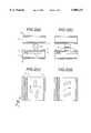
- FIG. 5is a plan view of a typical example of an electrode structure in a unit pixel of a liquid crystal display apparatus relating to the present invention
- FIG. 5(A)is a section view taken along line A-A'
- FIG. 5(B)is a section taken along line B-B' in FIG. 5;
- FIG. 6is a schematic view representing an example of a structure of a color filter substrate, FIG. 6(A) is a section view taken along line A-A' and FIG. 6(B) is a section view taken along line B-B' in FIG. 6;
- FIG. 7is a schematic view representing another example of a structure of a color filter substrate, FIG. 7(A) is a section view taken along line A-A' and FIG. 7(B) is a section view taken along line B-B' in FIG. 7, and FIG. 7(C) is an enlargement of the area C in FIG. 7;
- FIG. 8is a schematic view representing another example of a structure of a color filter substrate, FIG. 8(A) is a section view taken along line A-A' and FIG. 8(B) is a section view taken along line B-B' in FIG. 8, and FIG. 8(C) is an enlargement of the area C in FIG. 8;
- FIG. 9is a schematic circuit diagram of a liquid crystal display apparatus relating to the present invention.
- FIG. 10is a wave form diagram indicating an example of wave forms when a common electrode is made to operate as an alternating current electrode.
- FIG. 1is a schematic diagram of an active matrix type liquid crystal display apparatus relating to the present invention
- FIG. 5illustrates the structures of the thin film transistor (referred to hereinafter as a TFT) and respective electrodes in a unit pixel of the above panel display.
- a TFTthin film transistor
- the active matrix type liquid crystal display apparatuscomprises a pair of substrates 7, 7', a liquid crystal layer formed by liquid crystal molecules 6 interposed between the substrates, plural scanning electrodes 12, plural image signal electrodes 3 which cross the plural scanning electrodes 12 to form a matrix shape, pixel electrodes 4 formed closely and in parallel to the image signal electrodes 3, and plural TFT 14, which are active elements, formed at points where the scanning electrodes 12 cross the image signal electrodes and the pixel electrodes 4, all of the above electrodes and the TFT being formed on the one substrate 7 of the pair of substrates.
- An insulating layeri.e.
- a silicon nitride layeris formed on the above members, and additionally an alignment layer 5 is applied onto the insulating layer.
- the alignment layer 5, which is composed of an organic composition,is provided at a boundary between the substrate 7 and the liquid crystal layer, and rubbing treatment is performed on the surface of the alignment layer.
- Common electrodes 1are formed between the pixel electrodes 4 and adjacent image signal electrodes 3 so as to generate an electric field 9 in parallel to the substrate between the pixel electrodes 4 and the common electrodes 1 formed in the active elements, as shown in FIG. 2(b).
- color filters 23 with a black matrixwere formed on the other one of the substrates, as shown in FIG. 1, polyimide was applied onto the surface of the color filters and rubbing treatment was performed thereon.
- FIG. 5A plan view from a direction perpendicular to the substrate is shown in FIG. 5 and schematic cross sectional views taken on the lines A--A, and B-B' in the plan view of a typical example of the electrode structure are shown in FIG. 5(A) and FIG. 5(B), respectively.
- the TFT 14is composed of pixel electrodes (source electrodes) 4, image signal electrodes (drain electrodes) 3, scanning electrodes (gate electrodes) 12, and amorphous silicon 13.
- the common electrodes 1, the scanning electrodes 12, the image signal electrodes 3, and the pixel electrodes 4were formed from the same metallic layer by making a pattern.
- Capacitance elements 16were formed by a structure, wherein the insulating layer 2 was interposed between the pixel electrode 4 and the common electrode 1 in a region between the two common electrodes 1, and another insulating layer 25 was also interposed between the alignment layer 5 and the pixel electrode 4, as shown in the A-A' cross sectional view in FIG. 5(A).
- the pixel electrodes 4are arranged among three common electrodes 1, as shown in the plan view of FIG. 5.
- the pixel pitchis laterally, i.e. between the image signal electrodes 3, 100 ⁇ m, and longitudinally, i.e. between the scanning electrodes 12, 300 ⁇ m.
- the above widthsare, respectively, 10 ⁇ m, 8 ⁇ m, and 8 ⁇ m.
- the portions of the pixel electrode 4 and the common electrode 1 extending in parallel to the longitudinal direction of the image signal electrode 3, which portion were formed independently by a respective unit pixel,were formed to be somewhat narrow, such as 5 ⁇ m and 6 ⁇ m, respectively.
- the narrow width of the electrodeprovides an increased possibility of a short or breakage of the circuit by contamination with dust or the like, but the defect is restricted to only a unit pixel, so that the defect is not likely to be extended to a line defect.
- An interval of 2 ⁇ mwas provided between the image signal electrode 3 and the common electrode 1 using an insulating layer.
- FIG. 6is a plan view as seen from a direction perpendicular to the substrate and schematic cross sectional views taken on lines A-A' and B-B' in the plan view are shown in FIG. 5 and FIGS. 6(A) and 6(B), respectively.
- a material prepared by mixing carbon and organic pigmentswas used as the material for the black matrix.
- the black matrix arranged in parallel to the scanning electrode 12was formed by the steps of applying the black matrix material (a) onto the substrate, exposing a pattern, and developing the pattern.
- the black matrix arranged in parallel to the image signal electrode 3was formed by the steps of applying the black matrix material (b) onto the substrate, exposing a pattern, and developing the pattern.
- Width of the black matrixwas 16 ⁇ m, and it was formed so not to enter into the pixel region from a center line through the width of the common electrode 1.
- the arrangement of the black matrix on the electrodes substrateis indicated as a window expressed by dashed lines in FIG. 5.
- the specific resistivities of the black matrix materials (a) and (b)were adjusted by controlling the mixed amounts of carbon.
- the specific resistivity of the material (a)was 2 ⁇ 10 9 ⁇ cm, and that of the material (b) was 8 ⁇ 10 7 ⁇ cm (both values were the specific resistivities after forming the black matrix, hereinafter the same specific resistivity was used).
- an active matrix type liquid crystal display apparatus relating to the present inventionwas obtained by forming the color filter 23 at respective regions R, G, and B by the steps of coating with photosensitive resins mixed with pigments, exposing a pattern, and developing.
- the present embodimentis the same as the embodiment 1 except for the following items.
- the present embodimentis the same as the embodiment 1 except for the following items.
- FIG. 7A schematic illustration of another example of the color filter substrate composition with a black matrix is shown in FIG. 7.
- the black matrixwhich was arranged in parallel to the image signal electrode 3, was formed with the material (b).
- the width of the black matrixwas somewhat narrower than that of the image signal electrode 3, i.e. 6 ⁇ m.
- the final width of the black matrix in parallel to the image signal electrode 3was 16 ⁇ m.
- the arrangement of the black matrix in the electrode substrateis indicated as a window expressed by the dashed lines in FIG. 5.
- the specific resistivity of the material (a) for the black matrixwas 3 ⁇ 10 10 ⁇ cm, and of the material (b) for the black matrix was 3 ⁇ 10 6 ⁇ cm.
- the present embodimentis the same as the embodiment 1 except for the following items.
- FIG. 8A schematic illustration of another example of the color filter substrate composition with a black matrix is shown in FIG. 8.
- the black matrixwhich was arranged in parallel to the image signal electrode 3, was formed with the material (b).
- the width of the black matrixwas somewhat narrower than that of the image signal electrode 3, i.e. 6 ⁇ m.
- the final width of the black matrix in parallel to the image signal electrode 3was 16 ⁇ m.
- the arrangement of the black matrix in the electrode substrateis indicated as a window expressed by the dashed lines in FIG. 5.
- the specific resistivity of the material (a) for the black matrixwas 5 ⁇ 10 9 ⁇ cm, and of the material (b) for the black matrix was 5 ⁇ 10 6 ⁇ cm.
- the present embodimentis the same as the embodiment 3 except for the following items.
- the black matrixwhich was arranged in parallel to the image signal electrode 3, was formed using chromium as the material (b).
- the width of the black matrixwas somewhat narrower than the image signal electrode 3, i.e. 6 ⁇ m.
- the black matrix made of chromiumwas coated with the material (a).
- the final width of the black matrix in parallel to the image signal electrode 3was 16 ⁇ m.
- the black matrix in parallel to the scanning electrode 12was formed.
- the arrangement of the black matrix in the electrode substrateis indicated as a window expressed by the dashed lines in FIG. 5.
- the specific resistivity of the material (a) for the black matrixwas 1 ⁇ 10 10 ⁇ cm.
- the active matrix type liquid crystal display apparatus obtained in the embodiment 5was used.
- An image signal electrode driving circuit 18was connected to the respective image signal electrodes 3, and a scanning electrode driving circuit 19 was connected to the respective scanning electrodes 12, as indicated in FIG. 9.
- a common electrode driving circuit 20was connected to the common electrode 1. All of the above driving circuits were controlled by a control circuit 17.
- a signal having informationis supplied to the image signal electrode 3, and a scanning signal is supplied to the scanning electrode 12 synchronously with the information signal.
- the information signalis transmitted from the image signal electrode 3 to the pixel electrode 4 via the TFT 14, and a voltage is supplied to the liquid crystal layer between the liquid crystal layer and the common electrode 1.
- a voltage wave formis also supplied to the common electrode 1, and a higher voltage by as much as the voltage supplied to the common electrode 1 is supplied to the liquid crystal layer.
- the supplied wave forms to respective wiring electrodesare indicated in FIG. 10.
- the amplitudes of the voltage wave formswere set as follows:
- V GH28.0
- the metallic portion of the black matrix in parallel to the image signal electrode 3was connected to the common electrode 1 so as to have always the same potential as the common electrode 1.
- the active matrix type liquid crystal display apparatuswherein the voltage to the common electrode 1 was supplied by an alternating current, had a wide viewing angle, which did not cause any reversion of the gradation in a range of 60 degrees in all four directions, i.e. right, left, up, and down, and no smear, resulting from cross talk generated along the image signal electrode 3, was observed.
- an active matrix type liquid crystal display apparatus of the in-plane switching mode typehaving a wide viewing angle and no cross talk generation can be obtained by making the shielding layer (black matrix), which is formed in parallel to the image signal electrodes in the in-plane switching mode, have the specific resistivity of, at the utmost, 10 8 ⁇ cm.
- an active matrix type liquid crystal display apparatus of the in-plane switching mode type, generating no cross talkcan be obtained by coating the black matrix with an insulating layer having the specific resistivity of at least 10 8 ⁇ cm.
Landscapes
- Physics & Mathematics (AREA)
- Nonlinear Science (AREA)
- Chemical & Material Sciences (AREA)
- Crystallography & Structural Chemistry (AREA)
- General Physics & Mathematics (AREA)
- Mathematical Physics (AREA)
- Optics & Photonics (AREA)
- Geometry (AREA)
- Liquid Crystal (AREA)
- Engineering & Computer Science (AREA)
- Computer Hardware Design (AREA)
- Theoretical Computer Science (AREA)
Abstract
Description
Claims (15)
Priority Applications (2)
| Application Number | Priority Date | Filing Date | Title |
|---|---|---|---|
| US09/139,117US6100956A (en) | 1995-10-26 | 1998-08-24 | Active matrix type liquid crystal display apparatus with a shielding layer having a specific resistance of a part thereof being less than 108 Ω·CM |
| US09/620,245US6392732B1 (en) | 1995-10-26 | 2000-07-20 | Active matrix type liquid crystal display apparatus |
Applications Claiming Priority (2)
| Application Number | Priority Date | Filing Date | Title |
|---|---|---|---|
| JP27864495AJP3200552B2 (en) | 1995-10-26 | 1995-10-26 | Active matrix type liquid crystal display |
| JP7-278644 | 1995-10-26 |
Related Child Applications (1)
| Application Number | Title | Priority Date | Filing Date |
|---|---|---|---|
| US09/139,117ContinuationUS6100956A (en) | 1995-10-26 | 1998-08-24 | Active matrix type liquid crystal display apparatus with a shielding layer having a specific resistance of a part thereof being less than 108 Ω·CM |
Publications (1)
| Publication Number | Publication Date |
|---|---|
| US5805247Atrue US5805247A (en) | 1998-09-08 |
Family
ID=17600158
Family Applications (3)
| Application Number | Title | Priority Date | Filing Date |
|---|---|---|---|
| US08/731,162Expired - LifetimeUS5805247A (en) | 1995-10-26 | 1996-10-10 | Liquid crystal display apparatus in which plural common electrodes are parallel to the pixel electrodes on the same substrate and a black matrix on the opposing substrate |
| US09/139,117Expired - LifetimeUS6100956A (en) | 1995-10-26 | 1998-08-24 | Active matrix type liquid crystal display apparatus with a shielding layer having a specific resistance of a part thereof being less than 108 Ω·CM |
| US09/620,245Expired - LifetimeUS6392732B1 (en) | 1995-10-26 | 2000-07-20 | Active matrix type liquid crystal display apparatus |
Family Applications After (2)
| Application Number | Title | Priority Date | Filing Date |
|---|---|---|---|
| US09/139,117Expired - LifetimeUS6100956A (en) | 1995-10-26 | 1998-08-24 | Active matrix type liquid crystal display apparatus with a shielding layer having a specific resistance of a part thereof being less than 108 Ω·CM |
| US09/620,245Expired - LifetimeUS6392732B1 (en) | 1995-10-26 | 2000-07-20 | Active matrix type liquid crystal display apparatus |
Country Status (3)
| Country | Link |
|---|---|
| US (3) | US5805247A (en) |
| JP (1) | JP3200552B2 (en) |
| KR (1) | KR100493374B1 (en) |
Cited By (23)
| Publication number | Priority date | Publication date | Assignee | Title |
|---|---|---|---|---|
| US5929958A (en)* | 1995-03-17 | 1999-07-27 | Hitachi, Ltd. | Liquid crystal display device with wide viewing angle characteristics |
| US6166795A (en)* | 1997-07-31 | 2000-12-26 | Mitsubishi Denki Kabushiki Kaisha | Liquid crystal display apparatus including a conductive layer on an array substrate thereof |
| US6219118B1 (en)* | 1995-05-08 | 2001-04-17 | Semiconductor Energy Laboratory Co., Ltd. | LCD with shield film formed at overlapping portion of bus lines and pixel electrode |
| US6271903B1 (en)* | 1997-01-23 | 2001-08-07 | Lg. Philips Lcd Co., Ltd. | Liquid crystal display device having a light shielding matrix |
| US6351300B1 (en)* | 1998-08-24 | 2002-02-26 | Hyundai Display Technology Inc. | Reflective LCD having high transmittance and method for manufacturing the same |
| US6417900B1 (en)* | 1997-03-21 | 2002-07-09 | Lg. Philips Lcd Co., Ltd. | Liquid crystal display unit with conductive light-shielding member having substantially the same potential as common electrode |
| US6421101B1 (en) | 1996-09-04 | 2002-07-16 | Semiconductor Energy Laboratory Co., Ltd. | Display device including a transparent electrode pattern covering and extending along gate & source lines |
| US20030234903A1 (en)* | 2002-06-25 | 2003-12-25 | Lg.Philips Lcd Co., Ltd. | In-plane switching mode liquid crystal display device |
| US20040066481A1 (en)* | 2002-10-04 | 2004-04-08 | Lg.Philips Lcd Co., Ltd. | In-plane switching mode liquid crystal display device and fabrication method thereof |
| US20040070717A1 (en)* | 2002-10-11 | 2004-04-15 | Lg.Philips Lcd Co., Ltd. | In-plane switching mode liquid crystal display device and fabrication method thereof |
| US20040085278A1 (en)* | 2002-10-31 | 2004-05-06 | Lg.Philips Lcd Co., Ltd. | In-plane switching mode liquid crystal display device having improved aperture ratio |
| US20040109103A1 (en)* | 1998-06-30 | 2004-06-10 | Hitachi, Ltd. | Liquid crystal display device |
| US20040114083A1 (en)* | 2002-12-11 | 2004-06-17 | Lg.Philips Lcd Co., Ltd | In-plane switching mode liquid crystal display device |
| US20040119915A1 (en)* | 2002-12-23 | 2004-06-24 | Lg.Philips Lcd Co., Ltd. | Liquid crystal display device and method of fabricating the same |
| US20040125057A1 (en)* | 2002-12-31 | 2004-07-01 | Lg.Philips Lcd Co., Ltd. | In-plane switching mode liquid crystal display device and method of fabricating the same |
| US20050073632A1 (en)* | 2003-10-07 | 2005-04-07 | American Panel Corporation | Flat panel display having integral heater, EMI shield, and thermal sensors |
| US20080042963A1 (en)* | 2006-07-03 | 2008-02-21 | Epson Imaging Devices Corporation | Liquid crystal device, method of driving liquid crystal device, and electronic apparatus |
| US20080074377A1 (en)* | 2006-09-26 | 2008-03-27 | Epson Imaging Devices Corporation | Driving circuit, liquid crystal device, electronic apparatus, and method of driving liquid crystal device |
| US7365819B2 (en) | 2002-12-10 | 2008-04-29 | Lg.Philips Lcd Co., Ltd. | In-plane switching mode liquid crystal display device and method of fabricating the same |
| US20080239223A1 (en)* | 2007-03-28 | 2008-10-02 | Epson Imaging Devices Corporation | Liquid crystal device, method of manufacturing liquid crystal device, and electronic apparatus |
| US20090015570A1 (en)* | 2007-07-10 | 2009-01-15 | Epson Imaging Devices Corporation | Electro-optical device, driving circuit, and electronic apparatus |
| US20100271570A1 (en)* | 2003-10-07 | 2010-10-28 | American Panel Corporation, Inc. | Flat panel display having an emi shield and thermal sensors |
| US20130194224A1 (en)* | 2012-01-27 | 2013-08-01 | Research In Motion Limited | Electronic device with capacitive touch-sensitive display |
Families Citing this family (10)
| Publication number | Priority date | Publication date | Assignee | Title |
|---|---|---|---|---|
| JP2888177B2 (en)* | 1994-09-28 | 1999-05-10 | 日本電気株式会社 | Liquid crystal display |
| JPH11174491A (en) | 1997-12-08 | 1999-07-02 | Nec Corp | Active matrix type liquid crystal display |
| JP3264270B2 (en)* | 1999-07-26 | 2002-03-11 | 日本電気株式会社 | Liquid crystal display |
| JP2002023171A (en)* | 2000-07-11 | 2002-01-23 | Nec Corp | Liquid crystal display device and manufacturing method therefor |
| JP4554798B2 (en)* | 2000-10-30 | 2010-09-29 | Nec液晶テクノロジー株式会社 | Liquid crystal display device and manufacturing method thereof |
| JP4165001B2 (en) | 2000-11-02 | 2008-10-15 | 富士ゼロックス株式会社 | Image display medium, image display device, and image display method |
| KR100448046B1 (en)* | 2000-12-05 | 2004-09-10 | 비오이 하이디스 테크놀로지 주식회사 | Reflective type fringe field swiching mode lcd |
| KR100484948B1 (en) | 2002-12-18 | 2005-04-22 | 엘지.필립스 엘시디 주식회사 | In-Plane Switching mode Liquid Crystal Display Device |
| KR101018558B1 (en)* | 2008-10-21 | 2011-03-03 | 하이디스 테크놀로지 주식회사 | LCD in transverse electric field mode |
| JP5333969B2 (en)* | 2009-09-15 | 2013-11-06 | 株式会社ジャパンディスプレイ | Liquid crystal devices and electronic equipment |
Citations (2)
| Publication number | Priority date | Publication date | Assignee | Title |
|---|---|---|---|---|
| US5248576A (en)* | 1989-09-18 | 1993-09-28 | Idemitsu Kosan Co., Ltd. | Method of producing color filter using a micellar disruption method |
| US5598285A (en)* | 1992-09-18 | 1997-01-28 | Hitachi, Ltd. | Liquid crystal display device |
Family Cites Families (9)
| Publication number | Priority date | Publication date | Assignee | Title |
|---|---|---|---|---|
| JPS5691277A (en)* | 1979-12-25 | 1981-07-24 | Citizen Watch Co Ltd | Liquiddcrystal display panel |
| US4538884A (en)* | 1981-07-10 | 1985-09-03 | Canon Kabushiki Kaisha | Electro-optical device and method of operating same |
| JPH0715536B2 (en)* | 1983-01-28 | 1995-02-22 | キヤノン株式会社 | Display panel |
| FI74871B (en)* | 1986-06-26 | 1987-12-31 | Sinisalo Sport Oy | SKYDDSKLAEDE. |
| GB9211282D0 (en)* | 1992-05-28 | 1992-07-15 | Philips Electronics Uk Ltd | Liquid crystal display devices |
| GB9211283D0 (en)* | 1992-05-28 | 1992-07-15 | Philips Electronics Uk Ltd | Liquid crystal display devices |
| TW477905B (en)* | 1995-06-14 | 2002-03-01 | Hitachi Ltd | Liquid crystal display device formed of high resistance black matrix with wide view angle |
| JP3289099B2 (en)* | 1995-07-17 | 2002-06-04 | 株式会社日立製作所 | Active matrix type liquid crystal display device and manufacturing method thereof |
| TW505801B (en)* | 1995-10-12 | 2002-10-11 | Hitachi Ltd | In-plane field type liquid crystal display device comprising a structure prevented from charging with electricity |
- 1995
- 1995-10-26JPJP27864495Apatent/JP3200552B2/ennot_activeExpired - Lifetime
- 1996
- 1996-10-10USUS08/731,162patent/US5805247A/ennot_activeExpired - Lifetime
- 1996-10-26KRKR1019960048754Apatent/KR100493374B1/ennot_activeExpired - Lifetime
- 1998
- 1998-08-24USUS09/139,117patent/US6100956A/ennot_activeExpired - Lifetime
- 2000
- 2000-07-20USUS09/620,245patent/US6392732B1/ennot_activeExpired - Lifetime
Patent Citations (2)
| Publication number | Priority date | Publication date | Assignee | Title |
|---|---|---|---|---|
| US5248576A (en)* | 1989-09-18 | 1993-09-28 | Idemitsu Kosan Co., Ltd. | Method of producing color filter using a micellar disruption method |
| US5598285A (en)* | 1992-09-18 | 1997-01-28 | Hitachi, Ltd. | Liquid crystal display device |
Cited By (72)
| Publication number | Priority date | Publication date | Assignee | Title |
|---|---|---|---|---|
| US6064460A (en)* | 1995-03-17 | 2000-05-16 | Hitachi, Ltd. | LCD with parallel field having counter electrode(s) at least equal to 1/2 width of video signal line |
| US5929958A (en)* | 1995-03-17 | 1999-07-27 | Hitachi, Ltd. | Liquid crystal display device with wide viewing angle characteristics |
| US7683978B2 (en) | 1995-05-08 | 2010-03-23 | Semiconductor Energy Laboratory Co., Ltd. | Display device |
| US20050099557A1 (en)* | 1995-05-08 | 2005-05-12 | Semiconductor Laboratory Co., Ltd., A Japan Corporation | Display device |
| US6219118B1 (en)* | 1995-05-08 | 2001-04-17 | Semiconductor Energy Laboratory Co., Ltd. | LCD with shield film formed at overlapping portion of bus lines and pixel electrode |
| US7110059B2 (en) | 1995-05-08 | 2006-09-19 | Semiconductor Energy Laboratory Co., Ltd. | Display device |
| US7190420B2 (en)* | 1995-05-08 | 2007-03-13 | Semiconductor Energy Laboratory Co., Ltd. | Display device |
| US20070153169A1 (en)* | 1995-05-08 | 2007-07-05 | Semiconductor Energy Laboratory Co., Ltd. | Display device |
| US6421101B1 (en) | 1996-09-04 | 2002-07-16 | Semiconductor Energy Laboratory Co., Ltd. | Display device including a transparent electrode pattern covering and extending along gate & source lines |
| US20050151891A1 (en)* | 1996-09-04 | 2005-07-14 | Semiconductor Energy Laboratory Co., Ltd., A Japan Corporation | Display Device |
| US7023502B2 (en) | 1996-09-04 | 2006-04-04 | Semiconductor Energy Laboratory Co., Ltd. | Semiconductor device having light-shielded thin film transistor |
| US8586985B2 (en) | 1996-09-04 | 2013-11-19 | Semiconductor Energy Laboratory Co., Ltd. | Display device |
| US8536577B2 (en) | 1996-09-04 | 2013-09-17 | Semiconductor Energy Laboratory Co., Ltd. | Display device |
| US20110163315A1 (en)* | 1996-09-04 | 2011-07-07 | Semiconductor Energy Laboratory Co., Ltd. | Display device |
| US7863618B2 (en) | 1996-09-04 | 2011-01-04 | Semiconductor Energy Laboratory Co., Ltd. | Display device |
| US7046313B2 (en) | 1996-09-04 | 2006-05-16 | Semiconductor Energy Laboratory Co., Ltd. | Semiconductor device including a source line formed on interlayer insulating film having flattened surface |
| US20060192201A1 (en)* | 1996-09-04 | 2006-08-31 | Semiconductor Energy Laboratory Co., Ltd. | Display device |
| US20100044714A1 (en)* | 1996-09-04 | 2010-02-25 | Semiconductor Energy Laboratory Co., Ltd. | Display device |
| US7646022B2 (en) | 1996-09-04 | 2010-01-12 | Semiconductor Energy Laboratory Co., Ltd. | Display device |
| US20020171780A1 (en)* | 1996-09-04 | 2002-11-21 | Hongyong Zhang | Display device |
| US6271903B1 (en)* | 1997-01-23 | 2001-08-07 | Lg. Philips Lcd Co., Ltd. | Liquid crystal display device having a light shielding matrix |
| US6587170B2 (en)* | 1997-01-23 | 2003-07-01 | Lg. Philips Lcd Co., Ltd. | Liquid crystal display device having a light shielding matrix |
| US6417900B1 (en)* | 1997-03-21 | 2002-07-09 | Lg. Philips Lcd Co., Ltd. | Liquid crystal display unit with conductive light-shielding member having substantially the same potential as common electrode |
| US6166795A (en)* | 1997-07-31 | 2000-12-26 | Mitsubishi Denki Kabushiki Kaisha | Liquid crystal display apparatus including a conductive layer on an array substrate thereof |
| US7599031B2 (en) | 1998-03-06 | 2009-10-06 | Hitachi, Ltd. | Liquid crystal display device |
| US20060152661A1 (en)* | 1998-03-06 | 2006-07-13 | Hitachi, Ltd. | Liquid crystal display device |
| US20040109103A1 (en)* | 1998-06-30 | 2004-06-10 | Hitachi, Ltd. | Liquid crystal display device |
| US6351300B1 (en)* | 1998-08-24 | 2002-02-26 | Hyundai Display Technology Inc. | Reflective LCD having high transmittance and method for manufacturing the same |
| US6452658B1 (en)* | 1998-08-24 | 2002-09-17 | Hyundai Display Technology Inc. | Reflective LCD having high transmittance and method for manufacturing the same |
| US7639336B2 (en) | 2002-06-25 | 2009-12-29 | Lg Display Co., Ltd. | In-plane switching mode liquid crystal display device |
| US6876420B2 (en) | 2002-06-25 | 2005-04-05 | Lg. Philips Lcd Co., Ltd. | In-plane switching mode liquid crystal display device |
| US20070064189A1 (en)* | 2002-06-25 | 2007-03-22 | Hyung-Ki Hong | In-plane switching mode liquid crystal display device |
| US20030234903A1 (en)* | 2002-06-25 | 2003-12-25 | Lg.Philips Lcd Co., Ltd. | In-plane switching mode liquid crystal display device |
| US20050275782A1 (en)* | 2002-06-25 | 2005-12-15 | Lg.Philips Lcd Co., Ltd. | In-plane switching mode liquid crystal display device |
| US7782434B2 (en) | 2002-06-25 | 2010-08-24 | Lg Display Co., Ltd. | In-plane switching mode liquid crystal display device |
| US20040066481A1 (en)* | 2002-10-04 | 2004-04-08 | Lg.Philips Lcd Co., Ltd. | In-plane switching mode liquid crystal display device and fabrication method thereof |
| US20050093805A1 (en)* | 2002-10-04 | 2005-05-05 | Lg. Philips Lcd Co.,Ltd. | In-plane switching mode liquid crystal display device and fabrication method thereof |
| US6839115B2 (en) | 2002-10-04 | 2005-01-04 | Lg. Philips Lcd Co., Ltd. | In-plane switching mode liquid crystal display device and fabrication method thereof |
| US7206052B2 (en) | 2002-10-04 | 2007-04-17 | Lg.Philips Lcd Co., Ltd | Method of fabricating an in-plane switching mode liquid crystal display device forming a second common electrode over the first common electrode and pixel electrode adjacent to the data line |
| US20040070717A1 (en)* | 2002-10-11 | 2004-04-15 | Lg.Philips Lcd Co., Ltd. | In-plane switching mode liquid crystal display device and fabrication method thereof |
| US20050099571A1 (en)* | 2002-10-11 | 2005-05-12 | Lg.Philips Lcd Co., Ltd. | In-plane switching mode liquid-crystal display device and fabrication method thereof |
| US7180565B2 (en) | 2002-10-11 | 2007-02-20 | Lg. Philips Co., Ltd. | In-plane switching mode liquid crystal display device having a storage electrode connected to the pixel electrode and under the color filter |
| US6839116B2 (en) | 2002-10-11 | 2005-01-04 | Lg.Philips Lcd Co., Ltd. | In-plane switching mode liquid crystal display device and fabrication method thereof |
| US20040085278A1 (en)* | 2002-10-31 | 2004-05-06 | Lg.Philips Lcd Co., Ltd. | In-plane switching mode liquid crystal display device having improved aperture ratio |
| US7365819B2 (en) | 2002-12-10 | 2008-04-29 | Lg.Philips Lcd Co., Ltd. | In-plane switching mode liquid crystal display device and method of fabricating the same |
| US6900862B2 (en) | 2002-12-11 | 2005-05-31 | Lg. Philips Lcd Co., Ltd. | In-plane switching mode liquid crystal display device |
| US20040114083A1 (en)* | 2002-12-11 | 2004-06-17 | Lg.Philips Lcd Co., Ltd | In-plane switching mode liquid crystal display device |
| US20050168677A1 (en)* | 2002-12-11 | 2005-08-04 | Lg Philips Lcd Co., Ltd. | Method of fabricating in-plane switching mode liquid crystal display device |
| US7605887B2 (en) | 2002-12-11 | 2009-10-20 | Lg Display Co., Ltd. | Method of fabricating in-plane switching mode liquid crystal display device |
| US6894744B2 (en) | 2002-12-23 | 2005-05-17 | Lg. Philips Lcd Co., Ltd. | Liquid crystal display device and method of fabricating the same |
| US7456927B2 (en) | 2002-12-23 | 2008-11-25 | Lg Display Co., Ltd. | Liquid crystal display device and method of fabricating the same |
| US20050212998A1 (en)* | 2002-12-23 | 2005-09-29 | Lg.Philips Lcd Co. Ltd. | Liquid crystal display device and method of fabricating the same |
| US20040119915A1 (en)* | 2002-12-23 | 2004-06-24 | Lg.Philips Lcd Co., Ltd. | Liquid crystal display device and method of fabricating the same |
| US6894756B2 (en) | 2002-12-31 | 2005-05-17 | Lg.Philips Lcd Co., Ltd. | In-plane switching mode liquid crystal display device and method of fabricating the same |
| US7580022B2 (en) | 2002-12-31 | 2009-08-25 | Lg Display Co., Ltd. | In-plane switching mode liquid crystal display device and method of fabricating the same |
| US20050200793A1 (en)* | 2002-12-31 | 2005-09-15 | Lg.Philips Lcd Co. Ltd. | In-plane switching mode liquid crystal display device and method of fabricating the same |
| US20040125057A1 (en)* | 2002-12-31 | 2004-07-01 | Lg.Philips Lcd Co., Ltd. | In-plane switching mode liquid crystal display device and method of fabricating the same |
| US20050073632A1 (en)* | 2003-10-07 | 2005-04-07 | American Panel Corporation | Flat panel display having integral heater, EMI shield, and thermal sensors |
| US7324176B2 (en)* | 2003-10-07 | 2008-01-29 | American Panel Corporation | Flat panel display having integral heater, EMI shield, and thermal sensors |
| US20100271570A1 (en)* | 2003-10-07 | 2010-10-28 | American Panel Corporation, Inc. | Flat panel display having an emi shield and thermal sensors |
| TWI383359B (en)* | 2006-07-03 | 2013-01-21 | Japan Display West Inc | A liquid crystal device, a driving method of a liquid crystal device, and an electronic device |
| US20080042963A1 (en)* | 2006-07-03 | 2008-02-21 | Epson Imaging Devices Corporation | Liquid crystal device, method of driving liquid crystal device, and electronic apparatus |
| US9240153B2 (en)* | 2006-07-03 | 2016-01-19 | Japan Display Inc. | Liquid crystal device, method of driving liquid crystal device, and electronic apparatus |
| US9697784B2 (en) | 2006-07-03 | 2017-07-04 | Japan Display Inc. | Liquid crystal device, method of driving liquid crystal device, and electronic apparatus |
| US7907111B2 (en)* | 2006-09-26 | 2011-03-15 | Epson Imaging Devices Corporation | Driving circuit, liquid crystal device, electronic apparatus, and method of driving liquid crystal device |
| US20080074377A1 (en)* | 2006-09-26 | 2008-03-27 | Epson Imaging Devices Corporation | Driving circuit, liquid crystal device, electronic apparatus, and method of driving liquid crystal device |
| US20080239223A1 (en)* | 2007-03-28 | 2008-10-02 | Epson Imaging Devices Corporation | Liquid crystal device, method of manufacturing liquid crystal device, and electronic apparatus |
| US8619225B2 (en)* | 2007-03-28 | 2013-12-31 | Japan Display West Inc. | Liquid crystal device with pixel electrode under the common electrode and thinner than drain electrode, method of manufacturing liquid crystal device, and electronic apparatus |
| US8081178B2 (en)* | 2007-07-10 | 2011-12-20 | Sony Corporation | Electro-optical device, driving circuit, and electronic apparatus |
| US20090015570A1 (en)* | 2007-07-10 | 2009-01-15 | Epson Imaging Devices Corporation | Electro-optical device, driving circuit, and electronic apparatus |
| US20130194224A1 (en)* | 2012-01-27 | 2013-08-01 | Research In Motion Limited | Electronic device with capacitive touch-sensitive display |
| US9262020B2 (en)* | 2012-01-27 | 2016-02-16 | Blackberry Limited | Electronic device with capacitive touch-sensitive display |
Also Published As
| Publication number | Publication date |
|---|---|
| KR100493374B1 (en) | 2005-08-17 |
| KR970022466A (en) | 1997-05-28 |
| JPH09120061A (en) | 1997-05-06 |
| US6100956A (en) | 2000-08-08 |
| JP3200552B2 (en) | 2001-08-20 |
| US6392732B1 (en) | 2002-05-21 |
Similar Documents
| Publication | Publication Date | Title |
|---|---|---|
| US5805247A (en) | Liquid crystal display apparatus in which plural common electrodes are parallel to the pixel electrodes on the same substrate and a black matrix on the opposing substrate | |
| US6980273B2 (en) | Active matrix type liquid crystal system | |
| KR100747357B1 (en) | Liquid crystal display device and method of fabricating the same | |
| KR100293811B1 (en) | LCD display device of IP PS mode | |
| US7982836B2 (en) | Liquid crystal display device | |
| US6787829B2 (en) | LCD panel | |
| KR100413577B1 (en) | Active matrix liquid crystal display device | |
| KR100921137B1 (en) | Liquid crystal display | |
| KR20030025169A (en) | Liquid crystal display panel, liquid crystal display device and liquid crystal television | |
| US6549258B1 (en) | Hybrid switching mode liquid crystal display device | |
| KR100317209B1 (en) | Active matrix liquid crystal display device | |
| US6124910A (en) | Active matrix liquid crystal display device with plural black matrix pixels openings | |
| JP3542023B2 (en) | Liquid crystal display | |
| JP3123273B2 (en) | Active matrix type liquid crystal display device and manufacturing method thereof | |
| KR100430376B1 (en) | Liquid crystal display | |
| US20080002078A1 (en) | In-plane switching active matrix liquid crystal display apparatus | |
| KR100446383B1 (en) | Apparatus for fringe field switching liquid crystal display | |
| KR19980077802A (en) | LCD and its manufacturing method | |
| JP2002221732A (en) | Liquid crystal display | |
| JPH09311324A (en) | Active matrix type liquid crystal display | |
| JP3655793B2 (en) | Liquid crystal display | |
| KR20030028971A (en) | Apparatus for thin film transistor liquid crystal display | |
| US11003031B2 (en) | Display apparatus | |
| KR20020056618A (en) | Liquid Crystal Display Panel for In-Plane Switching | |
| KR19980023382A (en) | Multi Scan Liquid Crystal Display |
Legal Events
| Date | Code | Title | Description |
|---|---|---|---|
| AS | Assignment | Owner name:HITACHI, LTD., JAPAN Free format text:ASSIGNMENT OF ASSIGNORS INTEREST;ASSIGNORS:OH-E, MASAHITO;ARATANI, SUKEKAZU;MATSUYAMA, SHIGERU;AND OTHERS;REEL/FRAME:008220/0927 Effective date:19960927 | |
| STCF | Information on status: patent grant | Free format text:PATENTED CASE | |
| FEPP | Fee payment procedure | Free format text:PAYOR NUMBER ASSIGNED (ORIGINAL EVENT CODE: ASPN); ENTITY STATUS OF PATENT OWNER: LARGE ENTITY | |
| FPAY | Fee payment | Year of fee payment:4 | |
| FPAY | Fee payment | Year of fee payment:8 | |
| FPAY | Fee payment | Year of fee payment:12 | |
| AS | Assignment | Owner name:PANASONIC LIQUID CRYSTAL DISPLAY CO., LTD., JAPAN Free format text:MERGER/CHANGE OF NAME;ASSIGNOR:IPS ALPHA SUPPORT CO., LTD.;REEL/FRAME:027363/0315 Effective date:20101001 Owner name:HITACHI DISPLAYS, LTD., JAPAN Free format text:COMPANY SPLIT PLAN TRANSFERRING ONE HUNDRED (100) PERCENT SHARE OF PATENT AND PATENT APPLICATIONS;ASSIGNOR:HITACHI, LTD.;REEL/FRAME:027362/0612 Effective date:20021001 Owner name:IPS ALPHA SUPPORT CO., LTD., JAPAN Free format text:COMPANY SPLIT PLAN TRANSFERRING FIFTY (50) PERCENT SHARE OF PATENTS AND PATENT APPLICATIONS;ASSIGNOR:HITACHI DISPLAYS, LTD.;REEL/FRAME:027362/0466 Effective date:20100630 |