US5805117A - Large area tiled modular display system - Google Patents
Large area tiled modular display systemDownload PDFInfo
- Publication number
- US5805117A US5805117AUS08/241,599US24159994AUS5805117AUS 5805117 AUS5805117 AUS 5805117AUS 24159994 AUS24159994 AUS 24159994AUS 5805117 AUS5805117 AUS 5805117A
- Authority
- US
- United States
- Prior art keywords
- display
- light box
- display system
- picture elements
- light
- Prior art date
- Legal status (The legal status is an assumption and is not a legal conclusion. Google has not performed a legal analysis and makes no representation as to the accuracy of the status listed.)
- Expired - Lifetime
Links
Images


Classifications
- H—ELECTRICITY
- H04—ELECTRIC COMMUNICATION TECHNIQUE
- H04N—PICTORIAL COMMUNICATION, e.g. TELEVISION
- H04N9/00—Details of colour television systems
- H04N9/12—Picture reproducers
- G—PHYSICS
- G02—OPTICS
- G02F—OPTICAL DEVICES OR ARRANGEMENTS FOR THE CONTROL OF LIGHT BY MODIFICATION OF THE OPTICAL PROPERTIES OF THE MEDIA OF THE ELEMENTS INVOLVED THEREIN; NON-LINEAR OPTICS; FREQUENCY-CHANGING OF LIGHT; OPTICAL LOGIC ELEMENTS; OPTICAL ANALOGUE/DIGITAL CONVERTERS
- G02F1/00—Devices or arrangements for the control of the intensity, colour, phase, polarisation or direction of light arriving from an independent light source, e.g. switching, gating or modulating; Non-linear optics
- G02F1/01—Devices or arrangements for the control of the intensity, colour, phase, polarisation or direction of light arriving from an independent light source, e.g. switching, gating or modulating; Non-linear optics for the control of the intensity, phase, polarisation or colour
- G02F1/13—Devices or arrangements for the control of the intensity, colour, phase, polarisation or direction of light arriving from an independent light source, e.g. switching, gating or modulating; Non-linear optics for the control of the intensity, phase, polarisation or colour based on liquid crystals, e.g. single liquid crystal display cells
- G02F1/133—Constructional arrangements; Operation of liquid crystal cells; Circuit arrangements
- G02F1/1333—Constructional arrangements; Manufacturing methods
- G02F1/13336—Combining plural substrates to produce large-area displays, e.g. tiled displays
- G—PHYSICS
- G02—OPTICS
- G02F—OPTICAL DEVICES OR ARRANGEMENTS FOR THE CONTROL OF LIGHT BY MODIFICATION OF THE OPTICAL PROPERTIES OF THE MEDIA OF THE ELEMENTS INVOLVED THEREIN; NON-LINEAR OPTICS; FREQUENCY-CHANGING OF LIGHT; OPTICAL LOGIC ELEMENTS; OPTICAL ANALOGUE/DIGITAL CONVERTERS
- G02F1/00—Devices or arrangements for the control of the intensity, colour, phase, polarisation or direction of light arriving from an independent light source, e.g. switching, gating or modulating; Non-linear optics
- G02F1/01—Devices or arrangements for the control of the intensity, colour, phase, polarisation or direction of light arriving from an independent light source, e.g. switching, gating or modulating; Non-linear optics for the control of the intensity, phase, polarisation or colour
- G02F1/13—Devices or arrangements for the control of the intensity, colour, phase, polarisation or direction of light arriving from an independent light source, e.g. switching, gating or modulating; Non-linear optics for the control of the intensity, phase, polarisation or colour based on liquid crystals, e.g. single liquid crystal display cells
- G02F1/133—Constructional arrangements; Operation of liquid crystal cells; Circuit arrangements
- G02F1/1333—Constructional arrangements; Manufacturing methods
- G02F1/1335—Structural association of cells with optical devices, e.g. polarisers or reflectors
- G02F1/133509—Filters, e.g. light shielding masks
- G02F1/133514—Colour filters
- G—PHYSICS
- G06—COMPUTING OR CALCULATING; COUNTING
- G06F—ELECTRIC DIGITAL DATA PROCESSING
- G06F3/00—Input arrangements for transferring data to be processed into a form capable of being handled by the computer; Output arrangements for transferring data from processing unit to output unit, e.g. interface arrangements
- G06F3/14—Digital output to display device ; Cooperation and interconnection of the display device with other functional units
- G06F3/147—Digital output to display device ; Cooperation and interconnection of the display device with other functional units using display panels
- G—PHYSICS
- G09—EDUCATION; CRYPTOGRAPHY; DISPLAY; ADVERTISING; SEALS
- G09F—DISPLAYING; ADVERTISING; SIGNS; LABELS OR NAME-PLATES; SEALS
- G09F9/00—Indicating arrangements for variable information in which the information is built-up on a support by selection or combination of individual elements
- G09F9/30—Indicating arrangements for variable information in which the information is built-up on a support by selection or combination of individual elements in which the desired character or characters are formed by combining individual elements
- G09F9/35—Indicating arrangements for variable information in which the information is built-up on a support by selection or combination of individual elements in which the desired character or characters are formed by combining individual elements being liquid crystals
- H—ELECTRICITY
- H04—ELECTRIC COMMUNICATION TECHNIQUE
- H04N—PICTORIAL COMMUNICATION, e.g. TELEVISION
- H04N5/00—Details of television systems
- H04N5/66—Transforming electric information into light information
- H04N5/70—Circuit details for electroluminescent devices
- H—ELECTRICITY
- H04—ELECTRIC COMMUNICATION TECHNIQUE
- H04N—PICTORIAL COMMUNICATION, e.g. TELEVISION
- H04N5/00—Details of television systems
- H04N5/74—Projection arrangements for image reproduction, e.g. using eidophor
- H04N5/7416—Projection arrangements for image reproduction, e.g. using eidophor involving the use of a spatial light modulator, e.g. a light valve, controlled by a video signal
- H04N5/7441—Projection arrangements for image reproduction, e.g. using eidophor involving the use of a spatial light modulator, e.g. a light valve, controlled by a video signal the modulator being an array of liquid crystal cells
- H—ELECTRICITY
- H04—ELECTRIC COMMUNICATION TECHNIQUE
- H04N—PICTORIAL COMMUNICATION, e.g. TELEVISION
- H04N9/00—Details of colour television systems
- H04N9/12—Picture reproducers
- H04N9/30—Picture reproducers using solid-state colour display devices
- H—ELECTRICITY
- H10—SEMICONDUCTOR DEVICES; ELECTRIC SOLID-STATE DEVICES NOT OTHERWISE PROVIDED FOR
- H10K—ORGANIC ELECTRIC SOLID-STATE DEVICES
- H10K59/00—Integrated devices, or assemblies of multiple devices, comprising at least one organic light-emitting element covered by group H10K50/00
- H10K59/10—OLED displays
- H10K59/18—Tiled displays
- G—PHYSICS
- G09—EDUCATION; CRYPTOGRAPHY; DISPLAY; ADVERTISING; SEALS
- G09G—ARRANGEMENTS OR CIRCUITS FOR CONTROL OF INDICATING DEVICES USING STATIC MEANS TO PRESENT VARIABLE INFORMATION
- G09G2300/00—Aspects of the constitution of display devices
- G09G2300/02—Composition of display devices
- G09G2300/026—Video wall, i.e. juxtaposition of a plurality of screens to create a display screen of bigger dimensions
- G—PHYSICS
- G09—EDUCATION; CRYPTOGRAPHY; DISPLAY; ADVERTISING; SEALS
- G09G—ARRANGEMENTS OR CIRCUITS FOR CONTROL OF INDICATING DEVICES USING STATIC MEANS TO PRESENT VARIABLE INFORMATION
- G09G2360/00—Aspects of the architecture of display systems
- G09G2360/04—Display device controller operating with a plurality of display units
- Y—GENERAL TAGGING OF NEW TECHNOLOGICAL DEVELOPMENTS; GENERAL TAGGING OF CROSS-SECTIONAL TECHNOLOGIES SPANNING OVER SEVERAL SECTIONS OF THE IPC; TECHNICAL SUBJECTS COVERED BY FORMER USPC CROSS-REFERENCE ART COLLECTIONS [XRACs] AND DIGESTS
- Y10—TECHNICAL SUBJECTS COVERED BY FORMER USPC
- Y10S—TECHNICAL SUBJECTS COVERED BY FORMER USPC CROSS-REFERENCE ART COLLECTIONS [XRACs] AND DIGESTS
- Y10S248/00—Supports
- Y10S248/917—Video display screen support
- Y10S248/919—Adjustably orientable video screen support
- Y—GENERAL TAGGING OF NEW TECHNOLOGICAL DEVELOPMENTS; GENERAL TAGGING OF CROSS-SECTIONAL TECHNOLOGIES SPANNING OVER SEVERAL SECTIONS OF THE IPC; TECHNICAL SUBJECTS COVERED BY FORMER USPC CROSS-REFERENCE ART COLLECTIONS [XRACs] AND DIGESTS
- Y10—TECHNICAL SUBJECTS COVERED BY FORMER USPC
- Y10S—TECHNICAL SUBJECTS COVERED BY FORMER USPC CROSS-REFERENCE ART COLLECTIONS [XRACs] AND DIGESTS
- Y10S345/00—Computer graphics processing and selective visual display systems
- Y10S345/903—Modular display
Definitions
- This inventionrelates to large area liquid crystal display systems and more specifically to display systems consisting of tiled arrays of liquid crystal display modules.
- Flat-panel displayshave achieved increasing acceptance in the marketplace, particularly with regard to small, hand-held television sets and portable computers. These displays are quite thin compared to conventional cathode ray tubes, yet are able to display video and other information.
- Various attemptshave been made to develop large area flat-panel displays as replacements for cathode ray tube display systems, particularly in situations where a great deal of information must be processed and displayed, such as in high definition television systems.
- flat-panel displaysare for television and computer displays, flat-panel displays can be used in any number of different applications, such as for advertising, status displays, video conferencing, highway signs, office directories or avionics' displays.
- U.S. Pat. No. 4,832,457which consists of a liquid crystal material sandwiched between a two-by-two glass plate array, and a cover glass plate centered over the array.
- the area under the cover glass platedefines a display area which contains picture elements and switching elements.
- the cover glass platehas a smaller major surface area than the combined major surface area of the glass plate array which produces perimeter regions on the major surface area of the four glass plate array that are not covered by the cover glass. Electrical contact pads for connecting external drive circuits to the switching and picture elements in the display area are disposed in this perimeter region.
- a disadvantage of this type of display systemis the limitation of a maximum of a two-by-two array of display components because of the requirement that perimeter regions exists on each of the array panels for the electrical contact pads.
- the size of the display areais severely restricted and is substantially dependent on the production technology of the liquid crystal display components.
- Current production technologycannot produce liquid crystal displays of sufficient size to form a large area two-by-two array display.
- this display systemis inadequate for large screen televisions or computer displays.
- U.S. Pat. No. 4,980,774which is assigned to the assignee of the present invention, and which is hereby incorporated by reference.
- U.S. Pat. No. 4,890,774describes a modular flat-screen, direct-view display system consisting of an array of liquid crystal displays, wherein each display can be formed by a polymer dispersed liquid crystal (PDLC) material sandwiched between two glass plates.
- Drive circuits located external to a display regionare connected to picture elements in the display region by row and column conductors and wrap-around vertical edge interconnects.
- PDLCpolymer dispersed liquid crystal
- the wrap-around vertical edge interconnectsare made by known metalization and photolithographic techniques on an adhesive side of a thin, insulating tape which has a thickness of approximately 0.001 inches.
- the tapeis bonded to the drive circuits, the vertical edges of the display, and the row and column conductors.
- the displaysare then arranged in close proximity to one another such that boundary picture elements proximate corresponding edges of adjacent displays are separated by substantially the same distance as adjacent picture elements within one of the displays.
- Such a display systemcan produce a displayed image that is substantially uninterrupted at the boundaries between displays.
- the module array of this display systemmay contain a sufficiently large number of display modules to produce a large area display.
- display modules according to U.S. Pat. No. 4,980,774 having the desired performance characteristicscan be relatively difficult to produce because of the present state-of-the-art performance of PDLC.
- Global or local backlighting systemshave been used for direct view modular displays.
- a global light systemrelies on a single light source system to provide illumination for the entire display system.
- An advantage of such a backlighting systemis the balanced light provided to each one of the liquid crystal displays in a corresponding display system.
- a disadvantage of global lightingis that the mechanical components necessary to support the individual displays and route the electrical wiring prevent the global backlight source from being positioned substantially close to the back of the displays. Since light tends to radiate in all directions from a source, the amount of light generated by the global backlight source that illuminates the displays decreases as the light source is positioned further away from each of the displays.
- local backlightinguses a plurality of local light sources with each light source providing illumination for a corresponding display in the system.
- Local light sourcescan be positioned in close proximity to the displays and therefore provide more efficient illumination than global backlight systems.
- Conventional passive matrix liquid crystal display systemsincorporate electrical circuits which display an image in substantially real time as a corresponding fully multiplexed video information signal is received by the display. For instance, if the video information signal is for a VGA compatible display of a PC-type personal computer, the video signal will contain 640-by-480 pixel data in a 60 Hz non-interlaced frame of 0.0167 seconds in duration.
- Conventional passive matrix displaysmust sequentially activate 640 picture elements or 1920 picture elements in each one of the 480 rows of a monochrome or color display, respectively, for a relatively short period of time during each one of the 0.0167 second frame periods. As a consequence, conventional displays have poor optical performance compared to conventional cathode ray tube (CRT) displays.
- CTRcathode ray tube
- Passive matrix liquid crystal displayscan achieve improved optical performance by utilizing a two-page scheme for displaying pixel information in the upper and lower half of the display simultaneously, which effectively doubles the activation time for each pixel in each frame in comparison with the fully multiplexed display technique described above.
- the resulting optical performanceis still inferior to that produced by a conventional CRT display.
- a readily manufacturable tiled modular display systemincludes an array of display modules that contain corresponding thin seal liquid crystal displays to produce a displayed image that appears seamless to a viewer.
- Each one of a plurality of module alignment devicesattach a respective one of the display modules to a global base plate.
- a housingsurrounds the base plate and display modules.
- a global cover glass assemblyis disposed above the display modules which in combination with the housing enclose and protect the display modules.
- Each one of the display modulescontains a display driver circuit board, a light source configuration and the thin seal display.
- the light source configurationincludes a light box, light sources extending through the light box and a translucent light box cover to balance the luminance output.
- the light sourcesmay be fluorescent lamp which extend through an entire row or column of the display modules.
- the light box coverutilizes an advantageous shape to improve the balance of the luminance output across the front surface of the light box cover.
- An optional pattern diffusermay be utilized adjacent the light box cover to enhance the uniformity of luminance output.
- the thin seal liquid crystal display in each display modulecomprises a liquid crystal material sandwiched by two substantially identically sized substrates.
- a thin perimeter sealwhich may be on the order of 0.005 inches, seals the two substrates together and contains the liquid crystal material in a display area.
- An array of picture elementsextend across the display area with boundary picture elements disposed proximate the thin seal and display edges.
- the separation between the boundary picture elements and the display edgeis such that the distance between corresponding boundary picture elements of adjacent display panels is equal to the distance of the picture elements contained in the display modules.
- the display modulesmay be positioned sufficiently close to one another to produce the tiled display system having a seamless appearance.
- At least one thin electrical conductorconnects electrical edge contacts of a corresponding thin seal display to the respective display driver circuit board.
- the global cover glass assemblymay contain a global black mask which comprises opaque row and column stripes on a transparent sheet.
- the opaque rows and columnspermit visibility of the picture elements and hide the mechanical seams of adjacent display modules.
- the global black maskfurther provides an alignment grid for alignment of each one of the display modules.
- the global cover glass assemblyalso includes a diffusion mask to provide an improved viewing angle of the display.
- Alignment of the display modules with respect to each other and the global black maskis achieved by the alignment devices.
- Each alignment devicecan move a corresponding display module in the horizontal and vertical direction relative to the array of display modules.
- the alignment devicesfacilitate the replacement of individual display modules without disturbing the alignment of the other display modules.
- the present inventionutilizes a contrast adjustment circuit to adjust and balance the contrast, brightness and transmission of each thin seal display.
- the present inventiondoes not require the use of thin seal displays manufactured with high tolerances at great expense. Since a tiled display configuration is used, display information may be provided to the display modules in a parallel manner. Correspondingly, an interface circuit having a lower multiplex rate is utilized to produce a display system with improved optical performance.
- FIG. 1is a personal computer system utilizing a tiled modular display system according to the present invention
- FIG. 2is a television system utilizing the tiled modular display system according to the present invention
- FIG. 3is a cross-sectional view of the tiled modular display system of FIGS. 1 and 2;
- FIG. 4is an exploded parts view of a display module used in the tiled display system of FIGS. 1 and 2;
- FIG. 5is a suitable thin seal liquid crystal display for use in the display module of FIG. 4;
- FIG. 6is a substrate assembly utilized in the manufacture of the thin seal display of FIG. 5;
- FIG. 7is a cross-sectional view of the substrate assembly of FIG. 6;
- FIG. 8is a magnified view of an epoxy bead used in the substrate assembly of FIGS. 6 and 7;
- FIG. 9is a top view of a reduced substrate assembly which may be used to form the thin seal display of FIG. 5;
- FIG. 10is a cross-sectional view of the reduced substrate assembly of FIG. 9;
- FIG. 11is a cross-sectional view of the thin seal display of FIG. 5;
- FIG. 12is a cross-section view of a light source configuration used in the display module of FIG. 4;
- FIG. 13is a top view of an optional pattern diffuser that may be used in the display module of FIG. 4;
- FIG. 14is an example array of luminance output values taken across the light source configuration of FIG. 12;
- FIG. 15is an array of correction values corresponding to the luminance output array of FIG. 14 which are used to produce the patterned diffuser of FIG. 13;
- FIG. 16is a flowchart of one suitable method for producing an appropriate shading for the pattern diffuser of FIG. 13;
- FIG. 17is a top view of adjacent corner portions of four thin seal displays in the tiled modular display system of FIGS. 1 and 2;
- FIG. 18is a top view of a suitable color filter mask which may be used in the display module of FIG. 4;
- FIG. 19is an exploded parts view of a global cover glass assembly in the tiled display system of FIG. 3;
- FIG. 20Ais a top view of a portion of a global black mask over corresponding corners of four adjacent display modules in the tiled display system of FIG. 3;
- FIG. 20Bis a cross-sectional view of the configuration in FIG. 2OA;
- FIG. 21is a cross-sectional view of an alignment device utilized in attaching a display module to a base plate of the tiled display system of FIG. 3;
- FIG. 22is a bottom view of the alignment device of FIG. 21;
- FIG. 23is a schematic diagram of the computer system of FIG. 1;
- FIG. 24is a contrast and transmission ratio chart of a suitable passive matrix liquid crystal display that may be used in the display module of FIG. 4;
- FIG. 25is a detailed schematic diagram of an interface circuit utilized in the tiled display system of the computer system in FIG. 23.
- FIG. 26is a flow chart of a method utilized by subcontrollers in the interface circuit of FIG. 25 to produce an image on the tiled display system of FIGS. 1 and 2.
- a tiled modular display system 1is shown connected to a computer system, such as a PC-type personal computer 10, in FIG. 1.
- the computer system 10includes an input device, such as a keyboard 20, a processing and storage unit 30, and an optional output device, such as the cathode ray tube (CRT) 40.
- the storage and processing unit 30contains a VGA-compatible video card 50 which has a passive matrix LCD driver output 60.
- the driver output 60is connected to the tiled display system 1 by a communications line 70.
- the video card 50also has an optional CRT output 56 for providing video information to the optional output device 40.
- the processing and storage unit 30is connected to the input device 20 and contains a 16-bit ISA bus which is well known in the PC personal computer art.
- the video card 50is connected to the ISA bus as represented by the dashed-line 35.
- the video card 50is normally contained within the processing and storage unit 30 and has been shown external to the processing and storage unit 30 for clarity.
- the computer system 10is shown as a personal computer, the computer system 10 may suitably be any one of the computer types well known in the art, such as a mainframe computer, a minicomputer, a workstation, or a personal computer.
- the video card 50may utilize a standard passive matrix LCD display VGA controller to generate LCD driver signals S containing row and column display information for 640-by-480 pixel frames in a 60 Hz non-interlaced manner.
- a standard VGA controller for the video card 50is a GGD6410 and GD6340 chipset available from Cirrus Logic of Freemont, Calif. Since the video format is 60 Hz non-interlaced, sixty frames of information are displayed on the tiled display system 1 and output device 40 every second. As a consequence, information for a video frame is transmitted and displayed every 0.0167 seconds (1 second/60 frames).
- the VGA video format used by the video card 50is compatible with available applications software.
- the video card data output 60transmits the LCD driver signals S to the tiled display system 1 over the communications line 70.
- suitable line buffersmay be utilized with the communications line 70.
- Suitable commercially available line buffersinclude those that conform to EIA standard RS-422, such as the line buffer transmitter and receiver pair, Part Nos. DS-26F31 and DS-26F32, from National Semiconductor, Inc. of Santa Clara, Calif.
- a video card optional CRT output 56transmits an analog signal corresponding to the LCD driver signals S to the output device 40.
- the tiled display system 1includes a housing 80 which contains an array of display modules 100.
- the display modules 100are shown separated by dashed lines 102 in FIG. 1 for clarity. However, to the viewer, the tiled display system 1 will appear to be one large display with substantially invisible seams between the display modules 100 to indicate that it is a modular display.
- the tiled display system 1contains 48 of the display modules 100 arranged into an array of six rows 105 and eight columns 110. First and last columns 115 and 120 of display modules 100 are shown on the extreme left and right side of the tiled display system 1, respectively.
- Each one of the display modules 100may contain 80 rows and 80 columns of pixels such that the tiled display system 1 contains 480 rows and 640 columns of pixels. Therefore, the tiled display system 1 is capable of displaying a standard 640-by-480 VGA pixel image.
- the depiction of the present invention with the array of 640-by-480 pixelsis for exemplary purposes only and is not intended to be a limitation of the invention.
- a display module 100 according to the present inventionmay contain a different sized array of pixels.
- the television system 200contains the tiled display system 1, a video formatting unit 210 and a video tuner, such as an NTSC television tuner 220.
- the video tuner 220may receive video signals from an external source, such as signals received by an antenna 230.
- the video tuner 220may also receive video signals from a local television cable system (not shown), or from playback units, such as a video cassette recorder 240, or a laser disk player (not shown).
- the video tuner 220provides an analog video signal of an image to be displayed to the video formatting unit 210.
- the video formatting unit 210operates in a substantially similar manner to the interface card 50 in FIG. 1 and generates a corresponding passive matrix LCD driver information signals S which are transmitted to the tiled display system 1.
- the tiled display system 1 of FIG. 2may contain a 8-by-6 array of display modules 100 to form 640-by-480 pixels as in the tiled display system 1 of FIG. 1. Such a configuration would be suitable to display broadcasted or recorded video signals in conventional NTSC television format. A greater number of rows and columns of pixels may be used in the tiled display system 1 to display images of high definition television (HDTV) video formats. Further, the array configuration and number of display modules 100 used to form the tiled display system 1 may be different to that shown in FIG. 2, to accommodate the potentially different aspect ratio of the HDTV formats.
- HDTVhigh definition television
- FIG. 3depicts a cross-sectional view of the tiled display system 1 taken along a line 3 of FIG. 1.
- each one of the modules 100is attached to a base plate 310 by respective module alignment devices 320.
- a first plurality of fluorescent lamp sockets 340are attached to the base plate 310 adjacent the first column 115 of display modules 100 as shown in FIG. 1.
- a second plurality of fluorescent lamp sockets(not shown) are attached to the base plate 310 adjacent the last column 120 of display modules 100 of FIG. 1.
- the second plurality of fluorescent lamp socketsare substantially in alignment with the first plurality of fluorescent lamp sockets 340 adjacent the first column 115 of display modules 100.
- a plurality of fluorescent lampsare connected to respective first and second lamps sockets 340, and extend through each of the rows 105 of the display modules 100 in FIG. 1 from the first column 115 to the last column 120.
- the filed display system 1may be configured with the fluorescent lamps extending through each one of the columns 110 of the display modules 100.
- the fluorescent lamps sockets 340would be disposed in top and bottom portions 342 and 344 of the tiled display system 1 adjacent the display modules 100.
- a rear plate 350is attached to, and held a fixed distance away, from the base plate 310 by suitable spacer devices well known in the art, such as standoffs 360.
- a fluorescent light ballast 370which is electrically connected to the lamp sockets 340 for illuminating the fluorescent lamps, may be disposed on the rear plate 350.
- a power supply 380such as those well known in the art, for providing electrical energy to the display modules 100 may also be disposed on the rear plate 350.
- the rear plate 350may further provide attachment mechanisms, such as hooks, so that the tiled display system 1 may be mounted on a wall.
- the tiled display system 1By mounting the fluorescent light ballast 370 and power supply 380 on the base plate 350, the tiled display system 1 effectively electrically isolates these power components from the display modules 100 that are attached to the base plate 310.
- the housing 80is secured to the rear plate 350.
- optional cooling fans(not shown) may be positioned on at least one side of the housing 80 to force air through the modules 100 to maintain relatively cool operating temperatures.
- a global cover glass assembly 330is spring-biased against the array of display modules 100 by standoffs 332 and 334 which secure the global cover glass assembly 330 to the base plate 310. Screws 345 and 346 and springs 347 and 348 of the standoffs 342 and 344 force the global cover glass assembly 330 in contact with the display modules 100.
- the housing 80 and global cover glass assembly 330operate to enclose and protect the array of modules 100.
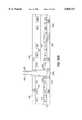
- FIG. 4depicts an exploded parts view of a suitable display module 100 for use in the tiled display system 1.
- Alternative suitable display module configurationsinclude those that utilize optically passive displays, such as liquid crystal and electrophoretic displays, and light emitting displays, such as electroluminescence and field active displays.
- the display module 100includes a display driver circuit board 410 attached to a base wall 421 of a light box 420.
- a light box cover 425is positioned adjacent an open end 429 of the light box 420.
- An optional patterned diffuser 428may be positioned adjacent the light box cover 425 as is shown in FIG. 4.
- a thin seal liquid crystal display 430is disposed adjacent the optional patterned diffuser 428.
- An optional color filter 440is disposed on top of, and may be laminated to, the thin seal display 430.
- a translucent compressible material(not shown) may be disposed between the thin seal display 430 and the patterned diffuser 428 such that when the global cover glass assembly 330 of FIG. 3 is biased against the display modules 100 by the screws 345 and 346 and springs 347 and 348, the thin seal displays 430 are slightly compressed toward the light box cover 425.
- the addition of the translucent compressible materialsfurther insures that the global cover glass assembly 330 is actually in contact with all portions of the entire display surface area of each one of the display modules 100.
- a suitable thin seal display 430has electrical edge contacts 432 which are electrically connected to a thin connector 450.
- the thin connector 450electrically connects the edge contacts 432 of the thin seal display 430 to driver circuits (not shown), such as those well known in the art, located on the driver board 410.
- the edge contacts 432 and corresponding thin connectors 450may extend across any number of the four sides of the thin seal display 430 and light box 420.
- a suitable thin connector 450is a flexible heat seal connector available from Elform of Reno, Nev., and has a thickness on the order of 0.001 inches.
- the light box 420is an open box having first and second horizontal walls 422 and 423, first and second vertical walls 426 and 427, and the base wall 421.
- the interior or exterior surfaces of the vertical horizontal and base walls 422, 423, 426, 427 and 421are painted with a suitable white reflective paint to maximize the amount of light generated out of the open end 429 of the light box 420.
- a plurality of corresponding pairs of holes 460are disposed on the first and second vertical walls 426 and 427, respectively, to permit the extension of a like plurality of light sources, such as fluorescent lamps 470, through the light box 420.
- the fluorescent lamps 470connect to, and are held in place by, the fluorescent lamp sockets 340 adjacent the first and last display module columns 115 and 120 of the tiled display system 1 as is shown in FIG. 3.
- the fluorescent lamps 470 and corresponding sockets 340may be disposed along the columns 110 of the display modules 100 in the tiled display system 1.
- the multiple lamp design per display module 100provides sufficient redundancy of light sources such that the failure of one of the fluorescent lamps 470 does not significantly effect readability of the display module 100.
- the fluorescent lamps 470should be suitably spaced and positioned from the rear of the thin seal display 430 to maximize luminance output and minimize luminance variation.
- Commercially available one-inch diameter fluorescent lamps, such as those available from General Electric Corporation or from Sylvania Corporationmay be used as the fluorescent lamps 470.
- driver circuits on the display driver board 410receive display signals from an interface circuit, such as the interface circuit described in detail below with regard to FIGS. 24-26.
- the driver circuit board 410provides the necessary driver signals on the thin connector 450 to the thin seal display 430 to produce a corresponding image.
- the light box 420 and light box cover 425utilize the light generated by the plurality of fluorescent lamps 470 to provide uniform backlighting of the display 430 to produce a direct view display.
- the color filter 440provides the necessary coloration to produce the desired color image.
- a suitable passive matrix thin seal display 430 for use in the display module 100is shown in FIG. 5.
- active matrix picture elementsmay be utilized in the displays 430 to achieve a further improvement in optical performance.
- a first transparent substrate 510such as a glass plate
- the second substrate 520is substantially the same size and shape of the first substrate 510.
- a liquid crystal materialsuch as a twisted nematic (TN) liquid crystal material, is sandwiched between the substrates 510 and 520.
- the liquid crystal materialis contained in the display 430 and protected from the environment by a thin seal 525 which secures the substrates together.
- TNtwisted nematic
- a matrix of picture elements 530are arranged in the panel 430 to form the pixels of the display module 100 and are described in greater detail below with regard to FIG. 6.
- Boundary picture elements 550are the picture elements 530 that are positioned adjacent edge surfaces 512 and 522 of the first and second substrates 510 and 520.
- the plurality of edge contacts 432are disposed on the substrate edge surfaces 512 and 522. Each one of the edge contacts 432 overlaps both of the edge surfaces 512 and 522, as well as the thin seal 525.
- the edge contacts 432are electrically connected to the picture elements 530 to enable control of the picture elements 530 to form the desired display image which is also described below with regard to FIG. 6.
- Each display module 100 in the tiled display system 1 of FIG. 1contains one thin seal display 430 in the manner shown in FIG. 4 to achieve a large area display with a seamless appearance.
- the distance between boundary picture elements 550 and the substrate edges 512 and 522 of the panel 430must be such that when two displays 430 are positioned adjacent one another, the spacing between corresponding boundary picture elements 550 of the two adjacent displays 430 is equal to the spacing between respective picture elements 530 within each of the displays 430. For example, if the respective picture elements 530 are positioned a distance of 0.014 inches from each other in a display 430 then boundary picture elements 550 of adjacent displays 430 should also be positioned 0.014 inches from each other.
- a spacing of 0.014 inchescan be achieved by positioning the boundary picture elements 550 a distance of approximately 0.005 inches from the substrate edges 512 and 522 and using a thin connector 450 of FIG. 4 attached to the edge contacts 432, having a thickness of approximately 0.001 inches.
- the display modules 100may be separated from one another such that the distance between the thin connectors 450 on the adjacent displays 430 is 0.002 inches. Therefore, the corresponding distance between adjacent boundary picture elements 550 of adjacent displays 430 is the desired 0.014 inches.
- FIG. 6depicts a substrate assembly 600 utilized in constructing the thin seal display 430 of FIG. 5.
- a cross-sectional view of the substrate assembly 600 taken along a line 7 in FIG. 6is shown in FIG. 7.
- the substrate assembly 600consists of top and bottom metalized substrates 610 and 620.
- Each one of the metalized substrates 610) and 620consists of an oversized substrate 630 which has a larger major surface area than that desired for the resulting surface area of the thin seal display 430.
- An outline dimension of the display 430is represented by a broken outline 605.
- a plurality of electrically conductive strips 640are disposed on respective first major surfaces 635 of the substrates 630.
- Both ends 641 and 642 of each of the electrically conductive strips 640may extend beyond the outline dimension 605 of the display 430. In the alternative, at least one of the ends 641 or 642 of each of the electrically conductive strips 640 should extend beyond the outline dimension 605.
- the electrically conductive strips 640may consist of metal, such as indium tin oxide (ITO), and may be formed on the substrate surface 635 by metalization and photolithographic techniques well known in the art. ITO is a preferred material as it is substantially transparent at particular resistance levels and has sufficient adhesion characteristics to glass.
- ITOindium tin oxide
- Electrically conductive pads 650are then coated over the electrically conductive strips 640 in areas 660 which cross over the outline dimension 605 in the manner as shown in FIGS. 6 and 7.
- the conductive pads 650 on the metalized substrate 610 in FIG. 6are shown in a shadow-line form as these pads are facing into the drawing.
- Sputtered chromeis a suitable material for the electrically conductive pads 650 because it is relatively easy to sputter and control, and adheres well to itself, ITO and glass.
- Alternative materials for the electrically conductive pads 650include nichrome and aluminum.
- the thickness of the electrically conductive pads 650may be on the order of 1500 angstroms when the thickness of the electrically conductive strips 640 is on the order of 300 angstroms. However, if the thickness of the electrically conductive strips 640 is greater than 1500 angstroms, the electrically conductive pads 650 may be omitted from the metalized substrates 610 and 620.
- the suitable thickness as described aboveis necessary to form the necessary electrical connection between the electrical edge contacts 432 and the picture elements 530. Each one of the picture elements 530 will be formed by an overlap region 690 of the electrically conductive strips 640 on the metalized substrates 610 and 620.
- a bead of a seal materialsuch as an epoxy 670
- a bead of a seal materialis dispensed in a defined pattern around the outline dimension 605 of the display 430 except for a small opening or gap 680 on the metalized substrate 620.
- the epoxy bead 670is laid over the substrate surface 635 and the electrically conductive pads 650.
- the gap 680is left open in the epoxy bead 670 to act as a filling port for the liquid crystal material.
- FIG. 8A magnified view of a portion of the epoxy bead 670 in a region 8 of the substrate assembly 600 of FIG. 6 is shown in FIG. 8.
- the epoxy bead 670must be precisely positioned over the outline dimension 605 of the thin seal display 430 and an interior edge 675 of the epoxy bead 670 must possess minimal edge variation in order to achieve the thin seal 625 in the display 430.
- the height of the epoxy bead 140must be maintained with minimal variation.
- the width of the epoxy bead 670need not be controlled in a precise manner, but must be determined in order to produce the thin seal 525 of FIG. 5.
- An adequate width and height of the epoxy bead 670is 0.014 inches and 21 microns, respectively.
- One suitable epoxy material for the epoxy beadis EPO-TEK B9021.
- the top and bottom metalized substrates 610 and 620are then arranged in a manner such that the electrically conductive strips 640 on the substrates 610 and 620 are oriented orthogonal with respect to one another as shown in FIGS. 6 and 7.
- the arranged metalized substrates 610 and 620are then heat cured at 150° C. for 15 minutes.
- the step of heat curing the arranged metalized substrates 610 and 620forms an epoxy seal which joins the two metalized substrates 610 and 620 together.
- the resulting structureis then filled with a liquid crystal material, such as a twisted nematic (TN) liquid crystal material, through the gap 680.
- a liquid crystal materialsuch as a twisted nematic (TN) liquid crystal material
- the gap 680is then sealed.
- One suitable method for sealing the gap 680 while maintaining the defined shape of the interior edge of the sealis to inject UV curable epoxy into the gap 680 while exposing only the gap to UV radiation by using a suitable mask and UV light source. Master Bond UV15-7 and Norland No. 61 are suitable UV curable epoxys to seal the gap 680.
- the major surfaces of substrate assembly 600 of FIGS. 6-8 containing the liquid crystal materialis reduced in a precise manner, such as by precision sawing through the top and bottom metalized substrate 610 and 620 to the outline dimension 605, to form a reduced substrate assembly 700 as shown in FIG. 9.
- the precision sawingshould cut through the epoxy seal formed from the epoxy bead 670 and the electrically conductive strips and pads 640 and 650.
- the assembled substrate 600may be reduced by precision sawing close to the outline dimension 605, such as to within 0.002 inches of the outline dimension 605, and then precision ground to the outline dimension 605.
- FIG. 10A cross-sectional view of the reduced substrate assembly 700 taken along a line 10 in FIG. 9 is shown in FIG. 10.
- the major surface area of the metalized substrates 610 and 620have been precision reduced, to form the substrates 510 and 520 of the display 430 of FIG. 5.
- the precision reduction of the epoxy seal formed from the epoxy bead 670 of FIGS. 6 and 7generates the thin seal 525.
- the thickness of the corresponding thin seal 525can be precisely controlled during the precision reduction process.
- Similar components of the substrate assembly 600 of FIGS. 6 and 7 and the reduced substrate assembly 700 of FIGS. 9 and 10are like numbered for clarity, for instance, the electrically conductive strips 640 and pads 650.
- the precision reduction processleaves edges 710 and 720 of the electrically conductive strips 640 and pads 650 exposed between the substrates edges surfaces 512 and 522. Also shown in FIG. 10, is a contained liquid crystal material 730.
- FIG. 11depicts a cross-sectional view of the thin seal display 430 of FIG. 5 taken along line 11.
- the display 430consists of the reduced substrate assembly 700 of FIGS. 9 and 10 with the deposited edge contacts 432.
- the edge contacts 432are electrically conductive contacts which are laid over the exposed edges 710 and 720 of the electrically conductive pads 650 and electrically conductive strips 640 in the manner as shown in FIG. 11.
- a suitable material for the edge contacts 432is sputtered chrome.
- One method for depositing the edge contacts 432is to place the reduced substrate assembly 700 into an edge sputter mask fixture (not shown) which has apertures of the size, shape, and in the positions where the edge contacts are to be formed. Metal is then sputtered on the fixture edge and through the fixture apertures to form the edge contacts 432.
- a suitable thin seal display 430may have a surface area dimension of 5.119 inches by 5.119 inches with an electrically conductive strip 640 configuration of 80 rows by 240 columns which form 80 by 80 color pixels.
- each of the thin seal displays 430 contained in the display modules 100it is desirable for each of the thin seal displays 430 contained in the display modules 100 to have uniform luminance output over the entire surface of the display 430 and with respect to the other displays 430. Lower luminance output at edge regions of the display modules 100 adjacent other display modules 100 would likely make the seams between the display modules 100 detectable by a viewer.
- luminance output measurements taken across the tiled display system 1should not vary by more than approximately 5% to 10% from an average value over short distances within a display module 100 or at boundaries between adjacent display modules 100.
- global light sources 470extend through the light box 420 of each display module 100 of FIG. 4, a lesser amount of luminance output will be generated out of the open end 429 of the light box 420 in edge regions adjacent horizontal walls 422 and 423 which extend parallel to the direction of the fluorescent lamps 470. Lower luminance output is generated in these regions because none of the fluorescent lamp 470 extend directly under these regions.
- FIG. 12depicts a cross-sectional view of a light source configuration 800 for use in the display module 100 of FIG. 4 which consists of the light box 420 and one suitable light box cover 425 to achieve the desired substantially uniform luminance output.
- the cross-sectional view of the light source configuration 800 in FIG. 12has been taken in a direction along the light box side sidewalls 423 and 424 of FIG. 4.
- Identical components of the light box 420 of FIGS. 4 and 12are like numbered for clarity, for example, the horizontal walls 422 and 423 and the base wall 421.
- the light box cover 425is attached to the light box 420 by support posts 810 and 820.
- the light box cover 425may be made of a suitable transparent material, such as polycarbonate or acrylic plastics.
- Horizontal edge regions 830 and 840 of the cover 425extend in a parallel direction to the fluorescent lamp 470 and receive less light from the fluorescent light lamps 470 than other regions of the light box cover 425, such as a center region 850.
- One suitable method to increase the luminance output in the horizontal edge regions 830 and 840is to include concave surfaces 860 and 862 and beveled edges 870 and 872 in those regions 830 and 840 of the light box cover 425.
- This shapecaptures a portion of light generated by the fluorescent lamps 470 and redirects the light out of the light box cover 425 in the regions 830 and 840.
- An optimal angle between the beveled edges 870 and 872, and the corresponding light box horizontal side walls 423 and 424is approximately 50° in order to provide sufficient luminance output from the regions 830 and 840.
- a diffusersuch as the patterned diffuser 428 of FIGS. 4 and 12 may be positioned adjacent the light box cover 425 on a side opposite the light box 420 to better improve the uniformity of the luminance output across the light source configuration 800.
- the patterned diffuser 428is a transparent sheet, such as a plastic or mylar sheet, with varying shading in respective regions to provide relatively dark shading in those regions where the luminance output of the light box cover 425 is greatest, and relatively light shading in those regions where the luminance output is the lowest.
- the addition of the patterned diffuser 428 to the light source configuration 800 of FIG. 12produces a light source having a substantially uniform luminance output across all regions including the horizontal edge regions 830 and 840.
- a suitable patterned diffuser 428which may be used with the light source configuration 800 of FIG. 12 is shown in FIG. 13.
- the patterned diffuser 428consists of a thin translucent plastic sheet 910 which contains a predetermined amount of shading in particular regions 920.
- the positions of the regions 920correspond to the respective positions of the picture elements 530 of the thin seal display 430 shown in FIG. 5.
- the shading in each of the patterned diffuser regions 920 in FIG. 13consists of different densities of dot patterns.
- the dot pattern density in region 930is greater than the dot pattern density in region 940.
- the region 930 of the patterned diffuser 428would block more light than the region 940.
- the dot patterns 920 of heavier densitieswould be positioned over those regions of the light box cover 425 with greater luminance output and the dot patterns 920 of finer densities would be positioned over those light box cover regions with lower luminance output to achieve a substantially uniform luminance output.
- the patterned diffuser 428 of FIG. 13utilizes three different densities of dot patterns to provide sufficient shading of light to produce the uniform light output.
- the patterned diffuser 428 of this inventionis not intended to be limited to any particular number of different amounts of shading.
- a large density dot pattern 950provides the greatest shading and is used primarily in the regions 920 in a center area 960 where the greatest luminance output of the light source configuration 800 of FIG. 12 is found.
- the regions 920 in a perimeter area 970 of the patterned diffuser 428 where the light source configuration 800 luminance output is lowesthave no dot patterns, such as, in region 972, or light density dot patterns, such as in region 974.
- a medium density dot pattern 976is used to provide a medium amount of shading in those regions 920 that are typically between the center area 960 and the perimeter area 970.
- the patterned diffuser 428is shown in FIG. 13 with dashed lines 980 separating the various regions 920 for ease of illustration only. Patterned diffusers 428 according to this invention should not have any demarcation of its regions 920. The shading of the patterned diffuser 428 should be specifically arranged for a particular light source configuration arrangement, such as the light source configuration 800 of FIG. 12, in order to achieve a maximum level of uniformity of the luminance output. A method of generating a suitable patterned diffuser 428 will now be described with reference to FIGS. 14-16.
- FIG. 14depicts an example array of luminance output values 1000 taken across the light source configuration 800 shown in FIG. 12.
- Each value 1010 in the array 1000corresponds to a relative amount of detected luminance output at a respective area of the light box cover 425.
- Each one of the respective light box cover areasprovides illumination for a corresponding picture element 530 in the thin seal display 430 of FIGS. 4 and 5.
- Each of the luminance output valuesare scaled values between "0" and "10" wherein a "10" indicates maximum luminance output from the light box cover 425 and "0" indicates no luminance output of the cover.
- region 1020 in the third row and fourth column of the array 1000corresponds to the picture element 530 located in the third row and fourth column of the display 430 of FIG. 4 and contains a luminance output value of "9".
- each value 1010 of the array 1000is bounded by a dashed box outline 1030 to assist in understanding the relationship between the array values 1010 and the respective regions of the light box cover 425 of FIG. 12 that correspond to positions of the thin seal display picture elements 530 as shown in FIG. 5.
- the array 1000is shown in FIG. 14 as having 10-by-10 values 1010 to account for a thin seal display 430 having a corresponding array of 10-by-10 picture elements 530, but it is not intended that the display 430 or the patterned diffuser 428 be limited to any particular number of picture elements or regions.
- a suitable display 430 and patterned diffuser 428 for the tiled display system 1may contain an array of 80-by-80 pixels and values 1010.
- the patterned diffuser 428should be shaded in a manner such that luminance output of the patterned diffuser 428 is equal in value to the lowest detected luminance output in the array 1000 of FIG. 14.
- a proper patterned diffuser 428 for the light source configuration 800 of FIG. 12 that is characterized by the array 1000should possess sufficient shading in the regions 920 as seen in FIG. 13 to produce a luminance output of value "7" across the entire patterned diffuser 428.
- FIG. 15depicts an array of correction values 1100 which may be used to generate an appropriate patterned diffuser 428 to operate with the light source configuration 800 of FIG. 12 to achieve a light source having a uniform luminance output of a value "7".
- Each correction value 1110 in the correction value array 1100corresponds to the amount of shading required in the corresponding patterned diffuser 428 of FIG. 13. For example, a value 1120 of "0" indicates that no shading is required in a corresponding region of the pattern diffuser while values of "1", “2” or “3” indicate varying amounts of shading from lightest to greatest, respectively.
- a correction value 1130 in the third row and fourth columnis a "2" which indicates the amount of shading for the luminance output value 1020 in the third row and fourth column of the array 1000 of FIG. 14.
- the correction values 1110 of FIG. 5are generated by subtracting from each corresponding value 1010 in the array 1000 of FIG. 14 the lowest detected luminance output value in the array 1000.
- the correction value "2"is generated by subtracting the lowest detected luminance output value of "7” from the luminance output value 1020 of "9". In this manner, the luminance value in each region of the light box cover 425 is corrected to a luminance output value of "7".
- FIG. 16One suitable routine 1200 for producing a proper patterned diffuser 428 for a particular light source configuration 800 of FIG. 12 is illustrated in FIG. 16.
- a light source configuration 800 containing a light box 420, a light box cover 425 and fluorescent lamp 470is assembled for testing.
- the luminance of each region that corresponds to a picture element 530 in the display 430 of FIG. 5is then measured in step 1220.
- the routine 1200then proceeds to step 1230, where a luminance distribution or array, such as the array 1000 of FIG. 14 is generated. Then in step 1240, the lowest luminance output value is identified from the array of measured luminance output values 1010. A correction value array 1100 of FIG. 15 is then generated in step 1250 by taking the difference between the corresponding measured luminance output values 1010 of FIG. 14 for the respective regions and the overall lowest measured luminance output value. The data is then formatted and transmitted to a laser printer in step 1260 where the correction values 1110 of FIG. 15 are transformed into a corresponding dot density shading 920 in the respective regions 925 on a transparent plastic sheet 910. The resulting shaded plastic sheet may then be used as the patterned diffuser 428 shown in FIG. 13, or a template used in the generation of the patterned diffuser 428.
- the tiled display system 1 of FIG. 1further utilizes specific spacing arrangements between the picture elements 530 of the displays 430 in order to achieve its seamless appearance.
- One suitable spacing arrangement of the picture elements 530 in a portion 1300 of the tiled display system 1 containing four adjacent corner portions of the thin seal displays 430 of FIG. 5is shown in FIG. 17.
- the picture elements 530are arranged into groups of three to form pixels 1310 which are suitable for use in a color display system.
- pixel 1320is formed by picture elements 1322, 1324 and 1326.
- Each one of the displays 430 of FIG. 17contains 80 rows by 240 columns of picture elements 530 which form 80 rows by 80 columns of pixels 1310.
- Each one of the three picture elements 530 in each one of the pixels 1310may be approximately 0.012 ⁇ 0.049 inches in size as shown by distances A and B, respectively, and may be separated from one another by 0.007 inches as shown by a distance C. Also, the separation between adjacent picture elements 530 of adjacent pixels 1310, such as picture elements 1326 and 1328 may be 0.014 inches as shown by a distance D. Likewise, the separation between corresponding boundary picture elements 550 of adjacent thin seal displays 430 should be 0.014 inches to achieve the seamless appearance. Thus, the separation between picture elements 1330 and 1332 as shown by a distance E is 0.014 inches. Such a 0.014 inches separation may be achieved where the boundary picture elements 550 are positioned substantially in contact with the thin seal 525, shown in FIG. 5, having a width of approximately 0.005 inches, using a 0.001 inches thick thin connector 450 attached to the edge contacts 432 on each display 430 and with adjacent display 430 positioned 0.002 inches apart from one another.
- FIG. 18illustrates a corner portion 1400 of a suitable color filter mask 440 which may be arranged on top of, or laminated to, a corresponding thin seal display 430 having pixels 1310 of three picture elements 530, as shown in FIG. 17, to produce the color display system.
- the color filter mask 440is a substantially transparent sheet or film, such as plastic or mylar, which contains a plurality of tinted parallel color stripes 1410.
- the number and placement of color stripes 1410will be equal to that of the columns of picture elements 530 or three times the number of pixels 1310 of the corresponding thin seal display 430.
- the corresponding color filter mask 440will possess 240 color stripes.
- the color stripes 1410 on the color filter mask 440are arranged into groups 1420, such as group 1430, consisting of a red stripe 1432, a green stripe 1434, and a blue color stripe 1436 each.
- the positioning and spacing of color stripes 1410 within each of the groups 1420is a function of the spacing of the columns of picture elements 530 that form the pixels 1310 of the thin seal display 430.
- the positions of the picture elements 530 of the pixels 1310 under the color stripes 1410are represented by dashed line boxes, such as dashed line box 1440 in FIG. 18.
- the picture elements 530 forming the pixels 1310 of the displays 430variably shutter the light produced by the light source configuration 800 of FIG.
- each pixel 1310will produce the appearance of the required colors of an image at a suitable viewing distance from the tiled display system.
- the color stripes 1410 shown in FIG. 18are wider than the width of the corresponding picture elements 530 to accommodate for the spreading of light transmitted through the picture elements.
- the color stripes 1410may be printed on the transparent sheet such that the adjacent stripes 1410 in each group 1420 overlap a small amount to form regions 1440. For example, if the picture elements are 0.012 inches wide and are separated by 0.007 inches as shown in FIG. 17, the overlap regions 1440 of a corresponding color filter mask 440 may be 0.002 to 0.003 inches wide.
- Substantially black stripes 1450separate the boundary stripes 1410 of adjacent group 1420 in order to inhibit the transmission of light in regions between the picture elements 530.
- the substantially black stripes 1450may have a width of 0.010 inches when the separation between boundary picture elements 530 of adjacent pixels 1310 is 0.014 inches as shown in FIG. 17. Such a configuration will allow for a 0.002 inch spreading of the light at the edges of the boundary picture elements 530 of adjacent pixels 1310.
- the substantially black stripes 1450may be produced by the overlaying of red, green and blue stripes.
- substantially black edge stripes 1460are disposed adjacent vertical edges 1470 of the color filter mask 440.
- Such black stripes 1460may have a width of 0.003 inches when the corresponding column of picture elements 530 have edges positioned 0.005 inches from the vertical mask edges 1470.
- the edge stripes 1460allow a 0.002 inches spreading of the light exiting the column of picture elements 530 adjacent the edges 1470.
- the width of the color stripes 1410should be at least the width of the corresponding picture elements 530.
- the color stripes 1410 in the color mask 440 of FIG. 18are oriented in the column direction, the color stripes 1410 and pixels 1310 may be arranged in the row direction as an alternative configuration of the present invention. Such an orientation may be utilized to improve the horizontal viewing angle of the corresponding tiled display system 1 shown in FIG. 1.
- the color filter mask 440need not contain color stripes 1410 but may contain individual tinted color blocks which cover corresponding picture elements 530 in the display 430. Further, the color mask 440 may be omitted from the display module 100 to produce a monochromatic gray scale display. In such an instance, each picture element 530 may be used as a corresponding pixel of the display system.
- the liquid crystal materialshould be chosen in conjunction with the configuration of the display 430 such that the display 430 normally prevents light transmission in the regions between the picture elements 530 that would otherwise partially illuminate the tinted stripes 1410 of the color filter mask 440. Such illuminations would reduce the color contrast, saturation and purity of the display module 100.
- the thin seal display 430 regions outside the electrically conductive strips 640 shown in FIG. 11may be coated with an opaque material to prevent light transmission in these regions between the picture elements 530.
- the global cover glass assembly 330 of FIG. 3is positioned in front of the array of display modules 100 and the corresponding color filter masks 440.
- An exploded parts view of a suitable global cover glass assembly 330is depicted in FIG. 19.
- the global cover glass assembly 330comprises a global front viewing screen or diffuser 1510, a glass plate 1520 and an optional global black mask 1530.
- the global front diffuser 1510 and black mask 1530may be attached to the respective major surfaces 1522 and 1524 of the glass plate 1520 by transparent adhesives, such as those known in the art.
- a global color filter(not shown) may be incorporated into the global cover glass assembly 330 in order to eliminate the need of the local color filter masks 440 in the display modules 100, shown in FIG. 4.
- Such a global color filtermay be constructed of one large sheet of a suitable material or an array of smaller color filter sheets which may be easier to manufacturer.
- the global front diffuser 1510may be a viewing screen well known in the liquid crystal display art which increases the viewing angle of the thin seal display 430 by distributing the light exiting the color filter 440 of the display 430 over a wider angle.
- the global front diffuser 1510should achieve sufficient light diffusion to provide the desired compromise between an adequate viewing angle and display contrast and brightness.
- the front diffuser 1510may optionally be positioned adjacent surface 1524 of the global cover glass assembly 330. In an alternative global cover glass assembly 330, the front diffuser 1510 may be omitted if the glass plate 1520 is suitably frosted to cause the desired light diffusion.
- the global black mask 1530consists of an array of row and column opaque stripes 1532 and 1534, respectively, on a transparent sheet 1536.
- the overlapping of the opaque stripes 1532 and 1534should be arranged to produce transparent mask openings 1538 that light may pass through.
- the size and alignment of the mask openings 1538 with respect to the pixels 1310, shown in FIG. 13,will now be described with reference to FIGS. 20A and 20B.
- FIG. 20Adepicts a portion 1550 of the global black mask 1530 positioned over the color filter mask 440 and picture elements 530 of corresponding corner pixels 1310 of four adjacent display modules 100 in the filed display system 1 of FIG. 1.
- the edges of the thin seal displays 430 of the four adjacent display modules 100are represented by edge shadow lines 1552, 1554, 1556 and 1558.
- the width and separation of the opaque stripes 1532 and 1534 in the global black mask 1530should correspond to the positioning and distance between the pixels 1310 of the respective display modules 100 in the tiled display system 1.
- FIG. 20BA cross-sectional view of the portion 1550 of the global black mask 1530 and the corresponding portions of the color filter masks 440 and thin seal displays 430 taken along a line B in FIG. 20A is shown in FIG. 20B.
- reference numbers concerning the cross-section of the thin seal displays 430are identical to those reference numbers used for the thin seal display 430 in FIG. 11 for clarity, for example, the substrates 510 and 520 and the electrically conductive stripes 640.
- the reference numbers regarding the color filter mask 440 and global black mask 1530 in FIGS. 18, 19 and 20Bare like numbered for clarity.
- the electrical edge contacts 432 in FIG. 11 to which the thin connectors 450 are attachedhave not been shown in FIG. 20B for clarity.
- the width of the color stripes 1410 of the color filter mask 440is slightly greater than the width of the electrically conductive strips 640 which define the width of the corresponding picture elements 530 to accommodate the spreading of the light exiting the picture elements 530 as is described below with reference to FIG. 18.
- the width and alignment of the global black mask openings 1538are greater than the width of the groups 1420 of colored stripes 1410 for a column of pixels 1310 to further accommodate the spreading of light exiting the color filter mask 440.
- a suitable width of the opaque stripes 1534is approximately 0.008 inches when the boundary stripes 1410 of adjacent groups 1420 are separated by 0.010 inches for columns of boundary picture elements 530 separated by a distance of approximately 0.014 inches as shown in FIG. 17.
- the color stripes 1410 of the color filter mask 440 and opaque stripes 1534 of the global black mask 330are represented as extending through their respective translucent sheets for clarity. However, the color stripes 1410 and opaque stripes 1534 should be disposed on the respective surfaces of the color filter mask 440 and global black mask 1530 that face one another to reduce the effects of parallax. Printing is a suitable method for disposing the stripes 1410 and 1530 on the respective surfaces.
- Opaque stripes 1534 having a width of 0.008 inchesare suitable to block the mechanical seams between adjacent thin seal displays 430 when the thin seal displays and corresponding display modules 100 are positioned 0.004 inches apart from one another.
- the opaque stripe 1534 having a width of 0.008 inches in FIG. 20Bwould overlap each one of the corresponding substantially black edge stripes of the color filter mask 440 by 0.002 inches if the respective thin seal displays 430 were separated by 0.004 inches.
- the spacing and width of the opaque stripes 1532 and 1534operate to block the mechanical seams between the adjacent display modules 100 of the tiled display system 1, and row and column conductors within an active matrix thin seal display.
- a viewer observing an assembled tiled display system 1 at close proximitywould see a large array of pixels 1310 separated by black stripes 1532 and 1534 of the global black mask 1530 without any detection of the actual display module 100 configuration beneath the global cover glass assembly 330.
- the pixels 1310 of the display modules 100must be substantially in alignment with the mask openings 1538 of the global black mask 1530 in the cover glass assembly 330 of FIG. 3.
- the stripes 1532 and 1534 of the global black mask 1530operate as a grid for alignment purposes. Small adjustments of the display modules 100 in the vertical and horizontal directions can be made by the alignment devices 320 that secure each of the display modules 100 to the base plate 310 as shown in FIG. 3.
- the alignment devices 320further permit the realignment of the display modules 100 whose alignment may change over time and temperature as a function of the material characteristics of the base plate 310 to which the display modules 100 are attached as is shown in FIG. 3.
- the more stable the base plate 310 materialthe less correction of the alignment due to time and temperature is required.
- a suitable stable base plate materialis mica enhanced aluminum.
- the global cover glass assembly 330is held against the display modules by a biasing force generated by the standoffs 342 and 344 shown in FIG. 3. As a consequence, the biasing force maintains direct contact and alignment between the display modules 100 and the global black mask 1530 independent of thermal expansion or contraction of the display modules 100.
- individual devicesmay be utilized to bias each one of the display modules 100 against a global cover glass assembly 330 having a fixed position.
- FIG. 21depicts a cross-sectional view of an assembly 1600 consisting of one suitable module alignment device 320 attached to a display module 100 and a corresponding portion of the base plate 310 of FIG. 3.
- a post 1610is mounted in a center region 1620 of the display module 100.
- the post 1610extends from the display module 100 through a hole 1615 in the base plate 310 and is slidably mounted to the alignment device 320 by a bushing 1630, a wisher 1635 and a screw 1640.
- the post 1610is permitted to move back and forth in a direction Z within the bushing 1630.
- the hole 1615should have a substantially larger diameter than a diameter of the post 1610 and bushing 1630 so as not to impede horizontal and vertical movement of the post 1610 by the alignment device 320.
- FIG. 21Also shown in FIG. 21 are compression devices 1650 that provide a biasing force which holds the display module 100 against the base plate 310.
- the compression devices 1650assist in maintaining alignment of the display module 100 when the tiled display system 1 is subjected to shock or vibration.
- One compression device 1650may be used for each one of the four corners of the display module 100. Since FIG. 21 is a cross-sectional view of the assembly 1600, only two of the four compression devices 1650 have been shown.
- Each compression device 1650contains a screw 1660 having a screw head 1665, and a coil spring 1670.
- the screw 1660 of each of the compression devices 1650extend through holes 1680 in the base plate 310 and are secured to the module 100.
- the diameter of the holes 1680are larger than the diameters of the screw 1660 to permit adjustment of the display module 100 in the vertical and horizontal direction by the alignment device 320.
- the springs 1670operate to push on the screw heads 1665 to pull the display module 100 toward the base plate 310.
- the compression devices 1650should provide a sufficient force to allow the display modules 100 to slide across the base plate 310 during thermal expansion or contraction of the display module 100 relative to the base plate 310.
- FIG. 22depicts a bottom view of the alignment device 320 of FIG. 21.
- the bashing 1630 holding the post 1610is fixed to an inner retainer 1710 by the screw 1640 and washer 1635 shown in FIG. 21.
- the post 1610slides within the bushing 1630.
- the inner retainer 1710is movably mounted in an outer retainer 1720 and is capable of sliding back and forth in directions X and Y within the outer retainer 1720 as shown in FIG. 22. Adjustment of the position of the inner retainer 1710 relative to the outer retainer 1720 is caused by horizontal and vertical screw adjuster assemblies 1730 and 1740, and a spring, such as a leaf spring 1745, which is mounted to the outer retainer 1720.
- Each of the screw adjuster assemblies 1730 and 1740includes a screw 1750, a corresponding screw cap 1752, a captured wedge-shaped block 1754 and a free wedge-shaped block 1756.
- Each screw 1750extends through a first hole 1760 in the outer retainer 1720, a threaded through hole 1765 of the captured block 1754, and a second hole 1770 in the outer retainer 1720.
- the screw cap 1752is locked onto the portion of the screw 1750 that extends beyond the second outer retainer hole 1770.
- rotation of the screw 1750advances or reverses the position of the captured block 1754 in the direction Y by the engagement of the threaded hole 1765 by threads of the screw 1750.
- Movement of the captured block 1754 in the Y directioncauses engagement of angle edge faces 1755 and 1757 of the wedge-shaped blocks 1754 and 1756, respectively.
- the free wedge-shaped block 1756 of the horizontal screw adjuster 1730is only permitted to move forwards or backwards in the direction X within a channel 1780 of the outer retainer 20, a force in the direction X is applied to the inner retainer 1710. This force counteracts the force generated by the spring 1745 on the inner retainer 1710 in the direction opposite to the direction X.
- the inner retainer 1710moves in the direction X.
- the post 1610 and corresponding display module 100will also move in the direction X.
- the amount of force on the free block edge 1780 generated by the rotation of the screw 1750is a function of the respective wedge angles of the blocks 1754 and 1756 and the spring 1745.
- the vertical screw adjuster assembly 1740operates in a substantially similar manner to the horizontal screw adjuster assembly 1730 and moves the inner retainer 1710 and the corresponding attached display module 100 forward or backward in the direction Y.
- the maximum displacement of the display module 100 in the directions of X or Yis limited by the widths of the channels 1780 of the outer retainer 1720 and the wedge angles of the respective blocks 1754 and 1756.
- the adjustment device 320 of FIGS. 21 and 22enables the horizontal and vertical alignment of the display module 100 with respect to adjacent display modules 100 and the global black mask 1530 within the global cover glass assembly 330 in the tiled display system 1 of FIG. 3.
- An alternative configuration of the alignment device 320may include a skew adjuster that operates in a substantially similar manner to the horizontal and vertical screw adjusters 1730 and 1740 to adjust the rotation orientation of the display module 100 about the post 1610.
- FIG. 23is a schematic representation of the computer system 10 of FIG. 1. Similar components in FIGS. 1 and 23 are like numbered for clarity, for example, the video card 50, the processing and storage unit 40 and the display modules 100.
- the video card 50is shown in the processing and storage unit 30 which has the attached input unit 20.
- the video card 50is connected to an interface circuit 1810 disposed in the tiled display system 1 and the optional output device 40.
- the interface circuit 1810receives the LCD driver signals S from the video card 50 and provides the corresponding row and column display information to the 8-by-6 array of passive matrix TN liquid crystal display modules 100.
- a data output portsuch as a standard PC computer serial output 1820.
- the data output port 1820is connected to a processing unit, such as a microprocessor 1830, located in a contrast adjustment circuit 1840 in the tiled display system 1.
- the microprocessor 1830is also connected to the interface circuit 1810 and a plurality of controllable potentiometers, such as individually addressable, digitally controlled potentiometers 1850 in the contrast adjustment circuit 1840.
- individual electrically erasable, programmable potentiometersmay be disposed in each one of the display modules 100.
- Suitable controllable potentiometers 1850are commercially available from Xicor, Inc. of Filipitas, Calif.
- the controllable potentiometers 1850are further connected to a power supply 1860, and a negative voltage input 1870 of each of the respective display modules 100 by individual power lines represented by a line 1880.
- the processing unit 1830facilitates contrast adjustment of the display modules 100 and provides stand alone operation of a self-test and calibration of the tiled display system 1.
- the stand alone self-test and calibration operationsmay utilize available fixed display patterns for optical and mechanical calibration, as well as verification of interface electronics operation of the interface electronics circuit 1810.
- the processing unit 1830communicates with suitable programmed routines in the processing and storage unit 30 to adjust the controllable potentiometers 1850 which vary the voltages applied to the negative voltage inputs 1870 of the display modules 100.
- the optical performance of the individual displays 430may be altered with respect to contrast and transmission by adjusting the applied voltage to the negative voltage inputs 1870 of the individual display modules 100.
- Contrastis the ratio of the measured luminance from an active or "on" picture element 530 of FIG. 5 as compared with the inactive or "off” picture element 530.
- Transmissionis the ratio of the measured luminance from an active picture element 530 as compared to the luminance supplied at the rear surface of the liquid crystal display 430.
- a representation of transmission and contrast curves 1910 and 1920 for a typical passive matrix TN display 430is shown in a chart 1900 in FIG. 24. Since the typical transmission and contrast characteristics may vary between displays 430, viewers will be able to see differences in the contrast and brightness of adjacent displays 430 in the tiled display system 1 absent any adjustment. Manufacturing tolerances of the thin seal displays 430 within the display modules 100 of FIG. 4 may be increased such that each display module 100 performs substantially identically to one another. However, a more cost effective technique to achieve identical performance is to adjust the transmission and contrast of each display module 100 by varying the display panel negative input voltages 1870 using the controllable potentiometers 1850 as shown in FIG. 17.
- the controllable potentiometers 1850may also be connected to, or contain, electrically alterable memory 1890 to permanently retain the last potentiometer setting when power is removed. As a result, when the tiled display system 1 is next powered on, each display module 100 will be returned to its previously adjusted voltage setting and corresponding optical performance.
- FIG. 25A detailed schematic representation of one suitable electronic interface circuit 1810 for controlling the image displayed in the tiled display system 1 is shown in FIG. 25.
- the LCD driver signals S containing the row and column display information from the communications line 70is provided to a timing control circuit 2010 and a first switch 2020.
- the switch 2020is capable of operating in a first or second position, and is further connected to a first frame memory unit 2030 and a second frame memory unit 2040. In a first position as shown in FIG. 25, the switch 2020 provides the row and column information to the first frame memory unit 2030, and in the second position as shown by a dashed line 2050, the row and column information is provided to the second frame memory unit 2040.
- the position of the first switch 2010is governed by the timing control circuit 2010 as shown by the control line 2055.
- the first and second memory units 2030 and 2040are each capable of storing a frame of display information from the received row and column information.
- the memory units 2030 and 2040are connected to first and second memory output buses 2060 and 2070, respectively.
- Each one of the memory units 2030 and 2040is capable of substantially simultaneously providing the stored row and column information for twelve respective 640 ⁇ 40 pixel sectors that comprise 640 ⁇ 480 pixels in the array of display modules 100 of the tiled display system 1.
- the first and second memory output buses 2060 and 2070are connected to a second switch 2080 in a manner as shown in FIG. 25.
- the switch 2080is capable of operating in a first or second position, and is further connected to a subcontroller information bus 2090. In a first position as shown in FIG. 25, the switch 2080 connects the second memory output bus 2070 to the subcontroller information bus 2090, and in the second position as shown by a dashed line 2085, the switch 2080 connects the first memory output bus 2060 to subcontroller information bus 2090.
- the position of the second switch 2080is also governed by the timing control circuit control line 2055.
- the subcontroller information bus 2090is connected to six subcontrollers 2111 through 2116 which are collectively referred to by reference number 2110. Each one of the subcontrollers 2110 is connected to a first and second shift register units 2120 and 2130 and to row selector inputs 2125 and 2135 for upper and lower 80-by-40 pixel sectors 2140 and 2150 for each one in the respective row of eight display modules 100 in the tiled display system 1 shown in FIG. 24.
- a dashed line 2145separates the upper and lower sectors 2140 and 2150 of the rows of display modules 100 illustration purposes only.
- Each one of the shift register units 2120 and 2130contains 640 elements and is further connected to 80 column inputs 2160 and 2170 for each one of the upper and lower pixel sectors 2140 and 2150 of the eight display modules 100 in the respective row of display modules 100.
- the shift registers 2120 and 2130may be double buffered shift registers well-known in the art which maintain a given output until a new sequence is shifted into the shift register and instructed to be applied to the outputs.
- only configurations for the shift register units 2120 and 2130, and corresponding row of display modules 100 for a first row 2180 and a sixth row 2190 of display modules 100have been shown.
- the configuration and operation of each of the second through fifth row of display modules 100 in the tiled display system 1 of FIG. 24 which have not been shownare substantially identical to those for the first and sixth rows 2180 and 2190.
- the timing control circuit 2010may consist of suitable programmed logic arrays to control the switch 2020 such that row and column information in the LCD driver signals S for each 640-by-480 image frame is sequentially alternatively directed to, and stored in, the first memory unit 2030 and the second memory unit 2040.
- a first LCD information framewould be directed to, and stored in, the first memory unit 2030
- the timing control circuit 2010would switch the first switch 2020 to its second position such that a second LCD information frame would be directed to the second memory unit 2040.
- a third received LCD information framewould then be directed to the first memory unit 2030 and so on.
- VGA compatible 640-by-480 pixel LCD driver signals Sthe LCD information frames are consecutively transmitted every 0.0167 seconds, and the timing control circuit 2010 will correspondingly switch the positions of the first switch 2055 every 0.0167 seconds.
- the second switch 2080is also operated by the timing control circuit 2010 such that the operating position of the first and second switches 2020 and 2080 are always changed substantially at the same time.
- the first and second switches 2020 and 2080are configured so that when the row and column display information is provided to the first memory unit 2030, the second memory output bus 2070 is connected to the subcontroller bus 2090.
- the first memory output bus 2060is connected to the subcontroller bus 2090.
- Such a configurationfacilitates the displaying of a just received frame of row and column display information while the next frame in the LCD driver signals S is being received.
- its memory output bus 2060 or 2070is connected to the subcontroller bus 2090 to provide the stored row and column display information to the associated subcontrollers 2110 by the second switch 2080.
- the memory units 2030 and 2040are configured in such a manner that each output of the outputs 2060 would substantially simultaneously provide row and column display information for each one of the twelve 640-by-40 pixel sectors in the 640-by-480 pixel tiled display system 1.
- Each one of the subcontrollers 2110controls a respective double sector of a 640-by-80 pixels displayed by a corresponding row of display modules 100.
- the subcontroller 2111controls the 640-by-80 pixel display formed by a first and second sector 2140 and 2150 of a row 2180 of the display modules 100.
- the first sector 2140contains pixel row numbers 1-40 and the second sector 2150 contains pixel row numbers 41-80 of the tiled display system 1.
- the operations of the subcontrollers 2111-2116may be performed by suitably programmed programmable logic arrays to minimize the number of components in, and complexity of, the interface circuit 1810.
- each one of the other subcontrollers 2112-2116is substantially identical to, and is performed at substantially the same time as, the operation of the subcontroller 2111.
- an internal counter or register in the subcontroller 2111 represented by the value nis initialized to zero in step 2210, and then incremented in step 2220. Then the subcontroller 2111 proceeds to perform the steps shown in columns 2224 and 2226 in a substantially parallel manner.
- the two columns 224 and 226 of the routine 2200perform substantially identical operations.
- the column 2224performs its operations on the first 40-by-640 pixel sector 2140 corresponding to the pixel row numbers 1-40, while the column 2226 performs its operations on the second 40-by-640 pixel sector 2150 corresponding to the pixel row numbers 41-80.
- step 2230 and 2240display information for the rows n and n+40 of the row 2180 of display modules 100 in FIG. 25 is retrieved from the associated memory unit 2030 or 2040 which is currently connected to the subcontroller information bus 2090.
- Each retrieved row display informationcharacterizes the display information for a complete 640 pixel row across the eight display modules 100 of row 2180.
- steps 2250 and 2260the two sets of row information corresponding to the 640 pixel rows are loaded into the respective upper sector shift register 2120 and lower sector shift register 2130, respectively.
- the two sets of row informationare then provided to the upper and lower sector column inputs 2160 and 2170, respectively, as provided in steps 2270 and 2280.
- the steps 2160 and 2170are required only if double buffered shift registers are utilized for the shift registers 2120 and 2130.
- the subcontroller 2111enables the upper and lower sector row selectors 2125 and 2135, respectively, in steps 2290 and 2300, to activate the corresponding rows of 640 pixels corresponding to the values n and n+40 in the display modules 100 of the first row 2180 of the tiled display system 1. For instance, at the time in the routine 2300 where the value n is 1, the first and forty-first row of 640 pixels will be activated within the row 2180 of display modules 100.
- the subcontroller 2111determines if the value n is equal to forty in step 2310. If the value n is not equaled to forty, then the routine 2200, increments the value n in step 2220 and repeats the display process of steps 2230-2300 to display the next two corresponding pixel rows in the upper and lower sectors 2140 and 2150 of the first row 2180 of display modules 100. In the alternative, if the value n is determined to be forty in step 2310, then all the display information from the associated memory unit 2030 or 2040 for the forty rows of each of the upper and lower sector 2140 and 2150 for an image frame has been retrieved and displayed in the first row 2180 of display modules 100. As a consequence, the routine 2200 reverts to step 2210 where the value n is reset to zero.
- Each of the other subcontrollers 2112 through 2116generates the portion of the display image on the respective row of the display modules 100 at substantially the same time as the subcontroller 2111 performs the routine 2200.
- the subcontrollers 2111-2116will be displaying twelve pixel rows of the image at any instant in time, wherein each one of the rows appears in the upper and lower sector 2140 or 2150 of the six rows of display modules 100 in the tiled display system 1.
- the twelve rows that are displayed at any instant in the respective upper or lower sectors of each row of display modules 100are separated from each other by forty pixel rows.
- the use of twelve forty-row sectors in FIG. 25is for exemplary purposes only and it is not intended that a tiled display system 1 according to the present invention be limited to using any particular number of sectors or pixel rows. Further, the sectors may be arranged in a column format instead of the row format of FIG. 25.
- the other memory unit 2030 or 2040will be receiving row and column display information from the LCD driver signals S for the next image frame.
- the high multiplex rate of 480:1 of pixel row information per every 0.0167 second framecan be reduced to a lower multiplex rate of 40:1 at the display modules 100 which enables the tiled display system 1 to allow gray-level encoding to be displayed and to achieve an improvement in optical performance.
- the interface circuit 1810is able to slow the timing requirements for the subcontrollers 2110 due to the tiled nature of the display system 1, low cost liquid crystal driver display circuits may be utilized in the subcontrollers 2110.
- any other type displaymay be used in the tiled display system, whether possessing a passive or active matrix display.
- the optional patterned diffusermay alternatively be positioned between the thin seal display and the color filter mask, or between the color filter mask and the global black mask.
Landscapes
- Physics & Mathematics (AREA)
- Engineering & Computer Science (AREA)
- Multimedia (AREA)
- Signal Processing (AREA)
- Nonlinear Science (AREA)
- General Physics & Mathematics (AREA)
- Crystallography & Structural Chemistry (AREA)
- Chemical & Material Sciences (AREA)
- Theoretical Computer Science (AREA)
- Optics & Photonics (AREA)
- Mathematical Physics (AREA)
- Human Computer Interaction (AREA)
- General Engineering & Computer Science (AREA)
- Devices For Indicating Variable Information By Combining Individual Elements (AREA)
- Liquid Crystal (AREA)
- Liquid Crystal Display Device Control (AREA)
- Transforming Electric Information Into Light Information (AREA)
Abstract
Description
Claims (60)
Priority Applications (10)
| Application Number | Priority Date | Filing Date | Title |
|---|---|---|---|
| US08/241,599US5805117A (en) | 1994-05-12 | 1994-05-12 | Large area tiled modular display system |
| PCT/KR1995/000055WO1995031876A1 (en) | 1994-05-12 | 1995-05-11 | Large area tiled modular display system |
| JP7529530AJP2758269B2 (en) | 1994-05-12 | 1995-05-11 | Tiled module type large screen display system |
| CN95190420ACN1052133C (en) | 1994-05-12 | 1995-05-11 | Large area tiled modular display system |
| EP99100817AEP0914011B1 (en) | 1994-05-12 | 1995-05-11 | Display module alignment device |
| EP95918207AEP0709014B1 (en) | 1994-05-12 | 1995-05-11 | Large area tiled modular display system |
| DE69514614TDE69514614T2 (en) | 1994-05-12 | 1995-05-11 | LARGE-SCALE DISPLAY SYSTEM WITH MODULAR PANELS |
| DE69525664TDE69525664T2 (en) | 1994-05-12 | 1995-05-11 | Device for aligning display modules |
| TW084110986ATW278172B (en) | 1994-05-12 | 1995-10-18 | |
| KR1019950704729AKR0164360B1 (en) | 1994-05-12 | 1995-10-27 | Large area tiled modular display system |
Applications Claiming Priority (1)
| Application Number | Priority Date | Filing Date | Title |
|---|---|---|---|
| US08/241,599US5805117A (en) | 1994-05-12 | 1994-05-12 | Large area tiled modular display system |
Publications (1)
| Publication Number | Publication Date |
|---|---|
| US5805117Atrue US5805117A (en) | 1998-09-08 |
Family
ID=22911363
Family Applications (1)
| Application Number | Title | Priority Date | Filing Date |
|---|---|---|---|
| US08/241,599Expired - LifetimeUS5805117A (en) | 1994-05-12 | 1994-05-12 | Large area tiled modular display system |
Country Status (8)
| Country | Link |
|---|---|
| US (1) | US5805117A (en) |
| EP (2) | EP0709014B1 (en) |
| JP (1) | JP2758269B2 (en) |
| KR (1) | KR0164360B1 (en) |
| CN (1) | CN1052133C (en) |
| DE (2) | DE69525664T2 (en) |
| TW (1) | TW278172B (en) |
| WO (1) | WO1995031876A1 (en) |
Cited By (158)
| Publication number | Priority date | Publication date | Assignee | Title |
|---|---|---|---|---|
| US5986622A (en)* | 1996-05-24 | 1999-11-16 | Lucent Technologies Inc. | Panel display of multiple display units for multiple signal sources |
| US6020863A (en)* | 1996-02-27 | 2000-02-01 | Cirrus Logic, Inc. | Multi-media processing system with wireless communication to a remote display and method using same |
| US6091394A (en)* | 1997-09-04 | 2000-07-18 | Lucent Technologies Inc. | Technique for holographic representation of images |
| US6129804A (en)* | 1998-05-01 | 2000-10-10 | International Business Machines Corporation | TFT panel alignment and attachment method and apparatus |
| US6151521A (en)* | 1997-11-19 | 2000-11-21 | Mitsubishi Denki Kabushiki Kaisha | Medical support system |
| US6193576B1 (en)* | 1998-05-19 | 2001-02-27 | International Business Machines Corporation | TFT panel alignment and attachment method and apparatus |
| WO2001020391A1 (en)* | 1999-09-15 | 2001-03-22 | Rainbow Displays, Inc. | Compensation for edge effects and cell gap variation in tiled flat-panel, liquid crystal displays |
| US6208319B1 (en)* | 1996-03-26 | 2001-03-27 | Fourie, Inc. | Display device |
| US6219011B1 (en)* | 1996-09-17 | 2001-04-17 | Comview Graphics, Ltd. | Electro-optical display apparatus |
| US6243059B1 (en)* | 1996-05-14 | 2001-06-05 | Rainbow Displays Inc. | Color correction methods for electronic displays |
| US6259429B1 (en)* | 1997-06-23 | 2001-07-10 | Seos Displays Limited | Multi-channel visual display apparatus |
| US6262694B1 (en)* | 1997-03-11 | 2001-07-17 | Fujitsu Limited | Image display system |
| US20010008303A1 (en)* | 1998-12-01 | 2001-07-19 | Sharp Kabushiki Kaisha | Semiconductor apparatus, a method of fabrication of the same, and a reinforcing tape used in fabrication of the same |
| US6271825B1 (en)* | 1996-04-23 | 2001-08-07 | Rainbow Displays, Inc. | Correction methods for brightness in electronic display |
| US6292157B1 (en)* | 1996-03-25 | 2001-09-18 | Rainbow Displays, Inc. | Flat-panel display assembled from pre-sorted tiles having matching color characteristics and color correction capability |
| US6297805B1 (en)* | 1997-08-29 | 2001-10-02 | Xerox Corporation | Multiple interacting computers interfaceable through a physical manipulatory grammar |
| WO2001088688A1 (en) | 2000-05-17 | 2001-11-22 | E-Magin Display Technologies Ltd. | Electronic billboard with reflective color liquid crystal displays |
| US20020003592A1 (en)* | 2000-07-10 | 2002-01-10 | Hett Charles L. | LCD tile display |
| WO2002047310A3 (en)* | 2000-11-10 | 2002-09-12 | Sarnoff Corp | Display tile structure using organic light emitting materials |
| US20020140629A1 (en)* | 2001-03-28 | 2002-10-03 | Sundahl Robert C. | Method and apparatus for tiling multiple display elements to form a single display |
| US20020156634A1 (en)* | 1999-05-04 | 2002-10-24 | Blum Ronald D. | Floor mat with voice-responsive display |
| US6476783B2 (en)* | 1998-02-17 | 2002-11-05 | Sarnoff Corporation | Contrast enhancement for an electronic display device by using a black matrix and lens array on outer surface of display |
| US6483482B1 (en)* | 1999-05-13 | 2002-11-19 | Samsung Sdi Co., Ltd. | Multi-display device |
| US6491560B1 (en) | 2000-05-25 | 2002-12-10 | Motorola, Inc. | Array tile system and method of making same |
| US20030016227A1 (en)* | 2001-07-19 | 2003-01-23 | Matthies Dennis L. | Adaptable large area display |
| US20030041427A1 (en)* | 2001-08-23 | 2003-03-06 | Koji Hattori | Multilayer ceramic electronic components and methods for manufacturing the same |
| US20030058211A1 (en)* | 2001-09-03 | 2003-03-27 | Sang-Il Kim | Liquid crystal display for wide viewing angle, and driving method thereof |
| US20030067418A1 (en)* | 2001-10-08 | 2003-04-10 | Mcclintock Dale Thomas | Integrated electronic display |
| US20030067437A1 (en)* | 2001-10-08 | 2003-04-10 | Mcclintock Dale Thomas | Digital playback device |
| US20030097478A1 (en)* | 2001-10-08 | 2003-05-22 | Imagearray, Ltd. | Method and system for synchronizing a presentation |
| US20030133037A1 (en)* | 2002-01-15 | 2003-07-17 | Hung-Lung Lee | TV wall for liquid crystal displays |
| KR100394235B1 (en)* | 2000-12-12 | 2003-08-06 | 현 석 조 | Multi-layer lighting display pannel and the activation apparatus |
| US6639638B1 (en) | 1999-08-27 | 2003-10-28 | International Business Machines Corporation | LCD cover optical structure and method |
| WO2003103470A1 (en)* | 2002-06-05 | 2003-12-18 | Intellimats, Llc | Modular protective structure for floor display |
| US20040001002A1 (en)* | 1999-05-04 | 2004-01-01 | Blum Ronald D. | Floor display system with interactive features |
| US20040021631A1 (en)* | 2002-07-30 | 2004-02-05 | Mclaughlin William J. | Apparatus for mounting and arranging a plurality of flat panel video displays |
| US20040021617A1 (en)* | 1999-05-04 | 2004-02-05 | Blum Ronald D. | Modular protective structure for floor display |
| US6690337B1 (en) | 1999-06-09 | 2004-02-10 | Panoram Technologies, Inc. | Multi-panel video display |
| US6731260B2 (en)* | 1997-10-13 | 2004-05-04 | Sanyo Electric Co., Ltd. | Display device |
| US20040085519A1 (en)* | 2000-12-22 | 2004-05-06 | Honeywell International Inc. | Distortion control for a seamless tile display system |
| US20040085478A1 (en)* | 2002-11-06 | 2004-05-06 | Vandruff Dean | Radio controlled tiled video display apparatus and method |
| US20040150582A1 (en)* | 2003-01-31 | 2004-08-05 | Universal Avionics Systems Corporation | Flat panel display having multiple display areas on one glass substrate |
| US20050020176A1 (en)* | 1999-02-17 | 2005-01-27 | Ammar Derraa | Field emission device fabrication methods, field emission base plates, and field emission display devices |
| US20050030267A1 (en)* | 2003-08-07 | 2005-02-10 | Gino Tanghe | Method and system for measuring and controlling an OLED display element for improved lifetime and light output |
| US20050062884A1 (en)* | 2003-09-22 | 2005-03-24 | Chang-Hsien Fan | System, apparatus and method for configuring identification of a display |
| US6873266B2 (en) | 1999-05-04 | 2005-03-29 | Intellimats, Llc | Electronic floor display |
| US20050078104A1 (en)* | 1998-02-17 | 2005-04-14 | Matthies Dennis Lee | Tiled electronic display structure |
| US20050105009A1 (en)* | 2003-10-07 | 2005-05-19 | American Panel Corporation, L.G. Philips Lcd | Flat panel display having an isolated EMI layer and integral heater and thermal sensors |
| US20050117054A1 (en)* | 2003-10-02 | 2005-06-02 | Funai Electric Co., Ltd. | Flat panel television |
| US6903706B1 (en)* | 2002-03-20 | 2005-06-07 | Matrox Graphics Inc. | Method and apparatus for multi-display of digital visual interfaces |
| US20050134474A1 (en)* | 1999-05-04 | 2005-06-23 | William Kokonaski | Display system for use on horizontal or non-horizontal surfaces |
| US20050140613A1 (en)* | 2002-02-06 | 2005-06-30 | Lowe Anthony C. | Tiled display with filter for uniform pixel brightness |
| US6917301B2 (en) | 1999-05-04 | 2005-07-12 | Intellimats, Llc | Floor display system with variable image orientation |
| US6940418B2 (en) | 1999-05-04 | 2005-09-06 | Intellimats, Llc | Electronic floor display cleaning system and protective cover |
| US6940496B1 (en)* | 1998-06-04 | 2005-09-06 | Silicon, Image, Inc. | Display module driving system and digital to analog converter for driving display |
| US20060049955A1 (en)* | 1999-05-04 | 2006-03-09 | Blum Ronald D | Electronic floor display with weight measurement and reflective display |
| US20060066511A1 (en)* | 2004-09-27 | 2006-03-30 | Clarence Chui | Systems and methods using interferometric optical modulators and diffusers |
| US20060066638A1 (en)* | 2000-09-19 | 2006-03-30 | Gyde Mike G | Methods and apparatus for displaying information |
| US20060097957A1 (en)* | 2002-11-29 | 2006-05-11 | Magink Display Technologies, Ltd. | Display panel and large display using such display panel |
| US20060171106A1 (en)* | 1998-11-11 | 2006-08-03 | Cho Young W | Portable computer and method for mounting a flat panel display device module |
| US7091933B2 (en) | 2001-10-08 | 2006-08-15 | Imagearray, Ltd | Electronic information display system |
| US7091927B1 (en)* | 2003-06-26 | 2006-08-15 | Rockwell Collins, Inc. | Display including tiles and a method of operating and manufacturing the same |
| US20060262279A1 (en)* | 1994-05-05 | 2006-11-23 | Iridigm Display Corporation | Interferometric modulation of radiation |
| KR100628435B1 (en)* | 1998-09-15 | 2006-12-04 | 삼성전자주식회사 | Assembly method of tiled liquid crystal display and tiled liquid crystal display |
| US7170468B2 (en) | 2001-02-21 | 2007-01-30 | International Business Machines Corporation | Collaborative tablet computer |
| US7205903B2 (en) | 1999-05-04 | 2007-04-17 | Intellimat, Inc. | Interactive and dynamic electronic floor advertising/messaging display |
| US20070097291A1 (en)* | 2005-10-31 | 2007-05-03 | Hewlett-Packard Development Company, Lp | Polymer dispersed liquid crystal |
| US20070097478A1 (en)* | 2005-10-31 | 2007-05-03 | Hewlett-Packard Development Company, L.C. | Charge responsive optical material |
| KR100666137B1 (en)* | 1998-10-20 | 2007-06-04 | 삼성전자주식회사 | Tiled liquid crystal display device and heat seal mounting method |
| US20070146354A1 (en)* | 2000-05-09 | 2007-06-28 | Sharp Kabushiki Kaisha | Data signal line drive circuit, drive circuit, image display device incorporating the same, and electronic apparatus using the same |
| US20070247404A1 (en)* | 2006-04-24 | 2007-10-25 | Yazaki Corporation | LCD unit, LCD apparatus, and method of setting drive voltage of LCD unit |
| KR100787299B1 (en)* | 2006-04-14 | 2007-12-20 | 오므론 가부시키가이샤 | Connector device and backlight assembly body use thereof |
| US20080049183A1 (en)* | 2003-10-07 | 2008-02-28 | American Panel Corporation | Flat panel display having integral metal heater optically hiddien behind an emi shield |
| US7358861B2 (en) | 1999-05-04 | 2008-04-15 | Intellimats | Electronic floor display with alerting |
| US20080181486A1 (en)* | 2007-01-26 | 2008-07-31 | Conversion Works, Inc. | Methodology for 3d scene reconstruction from 2d image sequences |
| US20080225059A1 (en)* | 2007-03-12 | 2008-09-18 | Conversion Works, Inc. | System and method for using off-screen mask space to provide enhanced viewing |
| US20080231634A1 (en)* | 2007-03-22 | 2008-09-25 | Honeywell International, Inc. | Intuitive modification of visual output from a multi-function display |
| US20080278408A1 (en)* | 1999-05-04 | 2008-11-13 | Intellimat, Inc. | Floor display systems and additional display systems, and methods and computer program products for using floor display systems and additional display system |
| US20090021532A1 (en)* | 2004-10-14 | 2009-01-22 | Gloege Chad N | Translation table |
| US20090065667A1 (en)* | 2007-08-27 | 2009-03-12 | Hewlett-Packard Development Company, L.P. | Monitor as a door |
| US7511630B2 (en) | 1999-05-04 | 2009-03-31 | Intellimat, Inc. | Dynamic electronic display system with brightness control |
| US20090096938A1 (en)* | 2007-10-10 | 2009-04-16 | Seiko Epson Corporation | Image correction apparatus, image display system, and image correction method |
| US20090153436A1 (en)* | 2007-12-14 | 2009-06-18 | Samsung Electronics Co. Ltd. | Multifunctional display apparatus |
| US7612859B2 (en) | 2005-10-31 | 2009-11-03 | Hewlett-Packard Development Company, L.P. | Ultra-violet radiation absorbing grid |
| US20090296194A1 (en)* | 2004-09-27 | 2009-12-03 | Idc, Llc | Optical films for directing light towards active areas of displays |
| US20090312884A1 (en)* | 2008-06-13 | 2009-12-17 | Li zheng min | Method for power sharing and controlling the status of a display wall |
| US20090322985A1 (en)* | 2006-09-01 | 2009-12-31 | Kiminori Mizuuchi | Multi-panel type liquid crystal display device |
| US20090322721A1 (en)* | 2003-09-19 | 2009-12-31 | E Ink Corporation | Methods for reducing edge effects in electro-optic displays |
| US7710632B2 (en) | 2004-09-27 | 2010-05-04 | Qualcomm Mems Technologies, Inc. | Display device having an array of spatial light modulators with integrated color filters |
| US20100201646A1 (en)* | 2006-03-31 | 2010-08-12 | Sony Corporation, A Japanese Corporation | E-ink touchscreen visualizer for home av system |
| US7777954B2 (en) | 2007-01-30 | 2010-08-17 | Qualcomm Mems Technologies, Inc. | Systems and methods of providing a light guiding layer |
| US7777691B1 (en)* | 2004-03-05 | 2010-08-17 | Rockwell Collins, Inc. | System and method for driving multiple tiled displays from a single digital video source |
| US7807488B2 (en) | 2004-09-27 | 2010-10-05 | Qualcomm Mems Technologies, Inc. | Display element having filter material diffused in a substrate of the display element |
| US7813026B2 (en) | 2004-09-27 | 2010-10-12 | Qualcomm Mems Technologies, Inc. | System and method of reducing color shift in a display |
| US20100265160A1 (en)* | 2009-04-16 | 2010-10-21 | Hajjar Roger A | Composite Screens Formed by Tiled Light-Emitting Screens |
| US7828616B2 (en) | 1998-10-23 | 2010-11-09 | Lg Display Co., Ltd. | Method of forming a portable computer having a flat panel display device |
| US7845841B2 (en) | 2006-08-28 | 2010-12-07 | Qualcomm Mems Technologies, Inc. | Angle sweeping holographic illuminator |
| US20100315574A1 (en)* | 2006-11-06 | 2010-12-16 | Kiminori Mizuuchi | Liquid crystal display device |
| US7855824B2 (en) | 2004-03-06 | 2010-12-21 | Qualcomm Mems Technologies, Inc. | Method and system for color optimization in a display |
| US20100328354A1 (en)* | 2009-06-26 | 2010-12-30 | Sony Computer Entertainment, Inc. | Networked Computer Graphics Rendering System with Multiple Displays |
| US7864395B2 (en) | 2006-10-27 | 2011-01-04 | Qualcomm Mems Technologies, Inc. | Light guide including optical scattering elements and a method of manufacture |
| US7893948B1 (en)* | 2004-10-14 | 2011-02-22 | Daktronics, Inc. | Flexible pixel hardware and method |
| US7898521B2 (en) | 2004-09-27 | 2011-03-01 | Qualcomm Mems Technologies, Inc. | Device and method for wavelength filtering |
| US7907319B2 (en) | 1995-11-06 | 2011-03-15 | Qualcomm Mems Technologies, Inc. | Method and device for modulating light with optical compensation |
| US7911428B2 (en) | 2004-09-27 | 2011-03-22 | Qualcomm Mems Technologies, Inc. | Method and device for manipulating color in a display |
| US7928928B2 (en) | 2004-09-27 | 2011-04-19 | Qualcomm Mems Technologies, Inc. | Apparatus and method for reducing perceived color shift |
| US7933475B2 (en) | 2006-02-17 | 2011-04-26 | Qualcomm Mems Technologies, Inc. | Method and apparatus for providing back-lighting in a display device |
| US20110102307A1 (en)* | 2004-10-14 | 2011-05-05 | Daktronics, Inc. | Sealed pixel assemblies, kits and methods |
| US8004743B2 (en) | 2006-04-21 | 2011-08-23 | Qualcomm Mems Technologies, Inc. | Method and apparatus for providing brightness control in an interferometric modulator (IMOD) display |
| US8040589B2 (en) | 2008-02-12 | 2011-10-18 | Qualcomm Mems Technologies, Inc. | Devices and methods for enhancing brightness of displays using angle conversion layers |
| US8040588B2 (en) | 2004-09-27 | 2011-10-18 | Qualcomm Mems Technologies, Inc. | System and method of illuminating interferometric modulators using backlighting |
| US8045256B2 (en) | 2004-09-27 | 2011-10-25 | Qualcomm Mems Technologies, Inc. | Method and device for compensating for color shift as a function of angle of view |
| US8045252B2 (en) | 2004-02-03 | 2011-10-25 | Qualcomm Mems Technologies, Inc. | Spatial light modulator with integrated optical compensation structure |
| US8049951B2 (en) | 2008-04-15 | 2011-11-01 | Qualcomm Mems Technologies, Inc. | Light with bi-directional propagation |
| US8061882B2 (en) | 2006-10-06 | 2011-11-22 | Qualcomm Mems Technologies, Inc. | Illumination device with built-in light coupler |
| US8068710B2 (en) | 2007-12-07 | 2011-11-29 | Qualcomm Mems Technologies, Inc. | Decoupled holographic film and diffuser |
| US20110291118A1 (en)* | 2010-06-01 | 2011-12-01 | Oh-Seob Kwon | Mother substrate for flat panel display apparatus and method of manufacturing the same |
| US8111446B2 (en) | 2004-09-27 | 2012-02-07 | Qualcomm Mems Technologies, Inc. | Optical films for controlling angular characteristics of displays |
| US20120032929A1 (en)* | 2010-08-06 | 2012-02-09 | Cho Byoung Gu | Modular display |
| US20120106098A1 (en)* | 2010-10-27 | 2012-05-03 | Ensil Tech Co., Ltd. | Flat Panel Display Apparatus and Method of Manufacturing the Same |
| US8193441B2 (en) | 2007-12-17 | 2012-06-05 | Qualcomm Mems Technologies, Inc. | Photovoltaics with interferometric ribbon masks |
| US8300304B2 (en) | 2008-02-12 | 2012-10-30 | Qualcomm Mems Technologies, Inc. | Integrated front light diffuser for reflective displays |
| US8344410B2 (en) | 2004-10-14 | 2013-01-01 | Daktronics, Inc. | Flexible pixel element and signal distribution means |
| US8362987B2 (en) | 2004-09-27 | 2013-01-29 | Qualcomm Mems Technologies, Inc. | Method and device for manipulating color in a display |
| US8368981B2 (en) | 2006-10-10 | 2013-02-05 | Qualcomm Mems Technologies, Inc. | Display device with diffractive optics |
| US20130176623A1 (en)* | 2012-01-06 | 2013-07-11 | Prysm, Inc | Portable display |
| US20130271940A1 (en)* | 2008-01-04 | 2013-10-17 | Nanolumens Acquisition, Inc. | Retractable display system and method of use |
| US8670171B2 (en) | 2010-10-18 | 2014-03-11 | Qualcomm Mems Technologies, Inc. | Display having an embedded microlens array |
| US20140168032A1 (en)* | 2012-12-14 | 2014-06-19 | Johanna Swan | Architecture for seamless integrated display system |
| US8791941B2 (en) | 2007-03-12 | 2014-07-29 | Intellectual Discovery Co., Ltd. | Systems and methods for 2-D to 3-D image conversion using mask to model, or model to mask, conversion |
| US8803762B2 (en)* | 2011-12-13 | 2014-08-12 | International Business Machines Corporation | System for automatically adjusting electronic display settings |
| US8848294B2 (en) | 2010-05-20 | 2014-09-30 | Qualcomm Mems Technologies, Inc. | Method and structure capable of changing color saturation |
| US8860712B2 (en) | 2004-09-23 | 2014-10-14 | Intellectual Discovery Co., Ltd. | System and method for processing video images |
| US8872085B2 (en) | 2006-10-06 | 2014-10-28 | Qualcomm Mems Technologies, Inc. | Display device having front illuminator with turning features |
| US8902484B2 (en) | 2010-12-15 | 2014-12-02 | Qualcomm Mems Technologies, Inc. | Holographic brightness enhancement film |
| US8928967B2 (en) | 1998-04-08 | 2015-01-06 | Qualcomm Mems Technologies, Inc. | Method and device for modulating light |
| US8971675B2 (en) | 2006-01-13 | 2015-03-03 | Qualcomm Mems Technologies, Inc. | Interconnect structure for MEMS device |
| US8979349B2 (en) | 2009-05-29 | 2015-03-17 | Qualcomm Mems Technologies, Inc. | Illumination devices and methods of fabrication thereof |
| US9013102B1 (en) | 2009-05-23 | 2015-04-21 | Imaging Systems Technology, Inc. | Radiation detector with tiled substrates |
| US9019183B2 (en) | 2006-10-06 | 2015-04-28 | Qualcomm Mems Technologies, Inc. | Optical loss structure integrated in an illumination apparatus |
| US9025235B2 (en) | 2002-12-25 | 2015-05-05 | Qualcomm Mems Technologies, Inc. | Optical interference type of color display having optical diffusion layer between substrate and electrode |
| US9110289B2 (en) | 1998-04-08 | 2015-08-18 | Qualcomm Mems Technologies, Inc. | Device for modulating light with multiple electrodes |
| US9395857B2 (en) | 2007-12-24 | 2016-07-19 | Tpk Holding Co., Ltd. | Capacitive touch panel |
| US9532431B2 (en) | 2015-02-02 | 2016-12-27 | Samsung Display Co., Ltd. | Organic light-emitting diode (OLED) display and method of manufacturing the same |
| CN107103851A (en)* | 2017-06-21 | 2017-08-29 | 郑州胜龙信息技术股份有限公司 | A kind of LED curved surfaces three-dimensional shows system |
| US9886877B2 (en)* | 2014-06-13 | 2018-02-06 | Barco N.V. | Adjustable display tile for tiled display |
| US20180130425A1 (en)* | 2016-11-09 | 2018-05-10 | Lg Electronics Inc. | Display apparatus |
| CN108898969A (en)* | 2018-08-27 | 2018-11-27 | 利亚德电视技术有限公司 | display screen |
| FR3066837A1 (en)* | 2017-05-29 | 2018-11-30 | Valeo Comfort And Driving Assistance | IMAGE GENERATING DEVICE AND HEAD DISPLAY COMPRISING SUCH A DEVICE |
| US20190244561A1 (en)* | 2016-11-17 | 2019-08-08 | Xi'an Novastar Tech Co., Ltd. | Pixel-by-pixel calibration method |
| US10459679B2 (en)* | 2008-01-04 | 2019-10-29 | Nanolumens Acquisition, Inc. | Display system and methods |
| RU2721369C1 (en)* | 2018-07-19 | 2020-05-19 | Юнилумин Груп Ко., Лтд. | Display device |
| US10789805B2 (en)* | 2015-06-10 | 2020-09-29 | Sg Gaming, Inc. | Casino machine having emotive lighting structures |
| CN112567523A (en)* | 2018-08-20 | 2021-03-26 | 三星电子株式会社 | Display device and method for manufacturing the same |
| US20220018015A1 (en)* | 2008-01-04 | 2022-01-20 | Nanolumens Acquisition, Inc. | Display Apparatus and Methods |
| US11262967B2 (en)* | 2019-11-04 | 2022-03-01 | Samsung Display Co., Ltd. | Display device and tiled display device including the same |
| US11610869B2 (en) | 2020-04-21 | 2023-03-21 | Samsung Display Co., Ltd. | Display device and tiled display device having the same |
| US20230214167A1 (en)* | 2008-01-04 | 2023-07-06 | Nanolumens Acquisition, Inc. | Display System and Methods |
Families Citing this family (27)
| Publication number | Priority date | Publication date | Assignee | Title |
|---|---|---|---|---|
| BE1011078A3 (en)* | 1997-04-01 | 1999-04-06 | Lorrymage Technologies B V B A | Smooth structure, in particular a screen that can be folded in an accordion structure and hinge intended for such a smooth structure |
| GB9724097D0 (en)* | 1997-11-15 | 1998-01-14 | Mort Christopher H J | Image control |
| KR100568014B1 (en)* | 1998-09-30 | 2006-06-28 | 삼성전자주식회사 | LCD panel of tiled LCD |
| KR100570507B1 (en)* | 1998-11-28 | 2006-09-14 | 삼성전자주식회사 | Tiled LCD |
| NO313119B1 (en)* | 2000-10-18 | 2002-08-12 | Dag Vilnes | Frame construction for planar structures |
| KR100796491B1 (en)* | 2001-12-29 | 2008-01-21 | 엘지.필립스 엘시디 주식회사 | LCD module with connector fixing part |
| KR100551029B1 (en)* | 2003-10-09 | 2006-02-13 | 삼성에스디아이 주식회사 | Chassis Base for Plasma Display and Plasma Display Using the Same |
| DE102005011411A1 (en)* | 2005-03-11 | 2006-09-14 | Siemens Ag | Luminous density distribution producing method for LCD-display, involves detecting and recording luminous density distribution of white picture, and detecting compensation picture from minimum luminous density and recorded distribution |
| CN1835662B (en)* | 2005-03-15 | 2011-11-09 | 友达光电股份有限公司 | Combination method of display and its protective panel |
| KR100720701B1 (en)* | 2005-09-09 | 2007-05-21 | 주식회사 디엠에스 | Cassette assembly for fluorescent lamp manufacturing |
| KR101323538B1 (en)* | 2005-11-14 | 2013-10-29 | 세미온 콘스테인 | Display module |
| CN101206327B (en)* | 2006-12-20 | 2011-11-30 | 欧睿控股股份有限公司 | Display in one piece and preparation method thereof |
| ITRM20090164A1 (en)* | 2009-04-10 | 2010-10-11 | Crisotech Italy S R L | MOUNTING STRUCTURE FOR VIDEO AND SIMILAR WALLS. |
| CN102095090B (en)* | 2009-12-09 | 2013-03-27 | 富士迈半导体精密工业(上海)有限公司 | Illuminating light fitting |
| DE102010055482B4 (en)* | 2010-12-22 | 2014-11-06 | Continental Automotive Gmbh | display unit |
| CN102368366A (en)* | 2011-10-11 | 2012-03-07 | 佛山市青松科技有限公司 | Outdoor display screen unit provided with protective panel |
| CN104285177B (en)* | 2012-05-16 | 2017-10-27 | 夏普株式会社 | Liquid crystal display |
| JP6428189B2 (en)* | 2014-11-18 | 2018-11-28 | レシップホールディングス株式会社 | LED indicator |
| KR102272059B1 (en) | 2015-02-09 | 2021-07-05 | 삼성전자주식회사 | Display module and display device comprising the same |
| US11682369B2 (en)* | 2017-09-20 | 2023-06-20 | Imax Theatres International Limited | Light emitting display with tiles and data processing |
| US10884278B2 (en)* | 2017-10-24 | 2021-01-05 | Palo Alto Research Center Incorporated | Liquid crystal temperature control by resistive heating |
| KR102415838B1 (en)* | 2017-11-28 | 2022-06-30 | 엘지디스플레이 주식회사 | Multi-panel display device |
| CN109410786A (en)* | 2018-12-27 | 2019-03-01 | 广州励丰文化科技股份有限公司 | The side active display of unilateral control |
| CN112951082B (en)* | 2019-12-10 | 2022-10-11 | 深圳市华胜软件技术有限公司 | Spliced screen |
| KR102806561B1 (en) | 2020-09-04 | 2025-05-13 | 삼성디스플레이 주식회사 | Display device and tiled display device including the same |
| KR20220075023A (en) | 2020-11-26 | 2022-06-07 | 삼성디스플레이 주식회사 | Display device and method for manufacturing the same, tiled display device comprising the same |
| NL2034314B1 (en)* | 2023-03-10 | 2024-09-24 | Van Berge Henegouwen Installaties B V | A computer implemented method for reducing the visual transition between visual media content displayed on a display of a display device and the environment surrounding the display device as well as such display device. |
Citations (41)
| Publication number | Priority date | Publication date | Assignee | Title |
|---|---|---|---|---|
| US3813673A (en)* | 1972-06-26 | 1974-05-28 | Trans Lux Corp | Display panel |
| US3821588A (en)* | 1973-03-08 | 1974-06-28 | Burroughs Corp | Display panel having flat side edges to permit butting together plural panels |
| US3840695A (en)* | 1972-10-10 | 1974-10-08 | Westinghouse Electric Corp | Liquid crystal image display panel with integrated addressing circuitry |
| US3861783A (en)* | 1973-06-28 | 1975-01-21 | Hughes Aircraft Co | Liquid crystal display featuring self-adjusting mosaic panel |
| US3961365A (en)* | 1974-10-24 | 1976-06-01 | Stewart-Warner Corporation | Color display device |
| US4006383A (en)* | 1975-11-28 | 1977-02-01 | Westinghouse Electric Corporation | Electroluminescent display panel with enlarged active display areas |
| US4114070A (en)* | 1977-03-22 | 1978-09-12 | Westinghouse Electric Corp. | Display panel with simplified thin film interconnect system |
| US4135959A (en)* | 1975-11-21 | 1979-01-23 | Westinghouse Electric Corp. | Method of manufacture of flat panel display device |
| US4156833A (en)* | 1977-05-24 | 1979-05-29 | Westinghouse Electric Corp. | Information display panel and method of fabrication |
| EP0035382A1 (en)* | 1980-02-29 | 1981-09-09 | Fujitsu Limited | Modular display device and display module therefor |
| US4408836A (en)* | 1980-02-28 | 1983-10-11 | Sharp Kabushiki Kaisha | Wide screen LCD panel with electrical terminal connections |
| EP0206178A1 (en)* | 1985-06-17 | 1986-12-30 | Casio Computer Company Limited | Liquid-crystal display apparatus |
| US4716403A (en)* | 1982-10-01 | 1987-12-29 | Seiko Epson Kabushiki Kaisha | Liquid crystal display device |
| WO1988000715A1 (en)* | 1986-07-22 | 1988-01-28 | Raychem Corporation | Large, high density display with segmented support |
| US4723119A (en)* | 1984-05-07 | 1988-02-02 | Futaba Denshi Kogyo Kabushiki Kaisha | Large-sized color display device |
| US4745404A (en)* | 1985-11-23 | 1988-05-17 | Edding Ag | Display device for planning purposes |
| US4771278A (en)* | 1986-07-28 | 1988-09-13 | Charles Pooley | Modular large-size forming lamp matrix system |
| DE3806421A1 (en)* | 1987-03-04 | 1988-11-24 | Citizen Watch Co Ltd | LIGHTING DEVICE FOR A LIQUID CRYSTAL DISPLAY DEVICE |
| US4800376A (en)* | 1986-01-13 | 1989-01-24 | Sony Corporation | Multiple display system |
| US4824215A (en)* | 1988-01-22 | 1989-04-25 | Xtalite Technology Limited/La Technologie Xtalite Limitee | Liquid crystal display apparatus |
| US4832457A (en)* | 1987-02-16 | 1989-05-23 | Hitachi, Ltd. | Multipanel liquid crystal display device |
| US4866530A (en)* | 1988-02-22 | 1989-09-12 | Kalua Kevin A | Multiple screen, modular video display projection system |
| US4945350A (en)* | 1985-07-09 | 1990-07-31 | Mitsubishi Denki Kabushiki Kaisha | Liquid crystal display unit |
| JPH02264291A (en)* | 1989-04-05 | 1990-10-29 | Matsushita Electric Ind Co Ltd | large liquid crystal display |
| US4980775A (en)* | 1988-07-21 | 1990-12-25 | Magnascreen Corporation | Modular flat-screen television displays and modules and circuit drives therefor |
| US4980774A (en)* | 1988-07-21 | 1990-12-25 | Magnascreen Corporation | Modular flat-screen television displays and modules and circuit drives therefor |
| US4982273A (en)* | 1988-07-21 | 1991-01-01 | Brody Thomas P | Modular flat-screen color television displays and modules and circuit drives therefor |
| US4982275A (en)* | 1988-07-21 | 1991-01-01 | Magnascreen Corporation | Modular flat-screen color television displays and modules and circuit drives therefor |
| US4982272A (en)* | 1988-07-21 | 1991-01-01 | Magnascreen Corporation | Modular flat-screen color television displays and modules and circuit drives therefor |
| JPH0377992A (en)* | 1989-08-21 | 1991-04-03 | Mitsubishi Electric Corp | large screen display device |
| WO1991008565A1 (en)* | 1989-11-24 | 1991-06-13 | Sean Hillen | Video display |
| US5067021A (en)* | 1988-07-21 | 1991-11-19 | Brody Thomas P | Modular flat-screen television displays and modules and circuit drives therefor |
| US5068740A (en)* | 1988-07-21 | 1991-11-26 | Magnascreen Corporation | Modular flat-screen television displays and modules and circuit drives therefor |
| US5079636A (en)* | 1988-07-21 | 1992-01-07 | Magnascreen Corporation | Modular flat-screen television displays and modules and circuit drives therefor |
| US5105183A (en)* | 1989-04-27 | 1992-04-14 | Digital Equipment Corporation | System for displaying video from a plurality of sources on a display |
| US5299017A (en)* | 1990-11-20 | 1994-03-29 | Pioneer Electronic Corporation | Screen fixing device of projection type television system |
| US5315695A (en)* | 1990-06-25 | 1994-05-24 | Kabushiki Kaisha Toshiba | Personal computer capable of altering display luminance through key operation |
| US5461510A (en)* | 1992-02-07 | 1995-10-24 | Vilnes; Dag | Method for assembling or disassembling of modules in a panel structure together with a panel structure in which the method is applied |
| US5508833A (en)* | 1992-07-10 | 1996-04-16 | Kabushiki Kaisha Topcon | Display apparatus sealed with a solvent-soluble fluorocarbon or fluorine-containing resin having an adhesive covalent bond-forming functional group |
| US5537127A (en)* | 1992-06-30 | 1996-07-16 | Kabushiki Kaisha Toshiba | Image monitor system console |
| US5557436A (en)* | 1994-05-12 | 1996-09-17 | Magnascreen Corporation | Thin seal liquid crystal display and method of making same |
Family Cites Families (7)
| Publication number | Priority date | Publication date | Assignee | Title |
|---|---|---|---|---|
| CH666560A5 (en)* | 1983-03-01 | 1988-07-29 | Tadeusz Bobak | DISPLAY DEVICE. |
| US4906071A (en)* | 1987-03-31 | 1990-03-06 | Matsushita Electric Industrial Co., Ltd. | Liquid crystal display device and video projector incorporating same with particular driving circuit connection scheme |
| JPH03259177A (en)* | 1990-03-08 | 1991-11-19 | Sanyo Electric Co Ltd | Surface light emitting device |
| JPH04248586A (en)* | 1991-02-05 | 1992-09-04 | Sanyo Electric Co Ltd | Manufacture of large-area liquid crystal panel |
| JPH04362615A (en)* | 1991-06-11 | 1992-12-15 | Seiko Instr Inc | Liquid crystal display device |
| JPH05193119A (en)* | 1992-01-21 | 1993-08-03 | Mitsubishi Heavy Ind Ltd | Ink scraping device |
| FR2687494B1 (en)* | 1992-02-18 | 1996-10-25 | Thomson Tubes Electroniques | MATRIX SCREEN IN PARTICULAR OF LARGE DIMENSIONS AND METHOD FOR THE PRODUCTION OF SUCH A MATRIX SCREEN. |
- 1994
- 1994-05-12USUS08/241,599patent/US5805117A/ennot_activeExpired - Lifetime
- 1995
- 1995-05-11CNCN95190420Apatent/CN1052133C/ennot_activeExpired - Lifetime
- 1995-05-11EPEP95918207Apatent/EP0709014B1/ennot_activeExpired - Lifetime
- 1995-05-11DEDE69525664Tpatent/DE69525664T2/ennot_activeExpired - Lifetime
- 1995-05-11DEDE69514614Tpatent/DE69514614T2/ennot_activeExpired - Lifetime
- 1995-05-11JPJP7529530Apatent/JP2758269B2/ennot_activeExpired - Lifetime
- 1995-05-11EPEP99100817Apatent/EP0914011B1/ennot_activeExpired - Lifetime
- 1995-05-11WOPCT/KR1995/000055patent/WO1995031876A1/ennot_activeCeased
- 1995-10-18TWTW084110986Apatent/TW278172B/zhnot_activeIP Right Cessation
- 1995-10-27KRKR1019950704729Apatent/KR0164360B1/ennot_activeExpired - Lifetime
Patent Citations (41)
| Publication number | Priority date | Publication date | Assignee | Title |
|---|---|---|---|---|
| US3813673A (en)* | 1972-06-26 | 1974-05-28 | Trans Lux Corp | Display panel |
| US3840695A (en)* | 1972-10-10 | 1974-10-08 | Westinghouse Electric Corp | Liquid crystal image display panel with integrated addressing circuitry |
| US3821588A (en)* | 1973-03-08 | 1974-06-28 | Burroughs Corp | Display panel having flat side edges to permit butting together plural panels |
| US3861783A (en)* | 1973-06-28 | 1975-01-21 | Hughes Aircraft Co | Liquid crystal display featuring self-adjusting mosaic panel |
| US3961365A (en)* | 1974-10-24 | 1976-06-01 | Stewart-Warner Corporation | Color display device |
| US4135959A (en)* | 1975-11-21 | 1979-01-23 | Westinghouse Electric Corp. | Method of manufacture of flat panel display device |
| US4006383A (en)* | 1975-11-28 | 1977-02-01 | Westinghouse Electric Corporation | Electroluminescent display panel with enlarged active display areas |
| US4114070A (en)* | 1977-03-22 | 1978-09-12 | Westinghouse Electric Corp. | Display panel with simplified thin film interconnect system |
| US4156833A (en)* | 1977-05-24 | 1979-05-29 | Westinghouse Electric Corp. | Information display panel and method of fabrication |
| US4408836A (en)* | 1980-02-28 | 1983-10-11 | Sharp Kabushiki Kaisha | Wide screen LCD panel with electrical terminal connections |
| EP0035382A1 (en)* | 1980-02-29 | 1981-09-09 | Fujitsu Limited | Modular display device and display module therefor |
| US4716403A (en)* | 1982-10-01 | 1987-12-29 | Seiko Epson Kabushiki Kaisha | Liquid crystal display device |
| US4723119A (en)* | 1984-05-07 | 1988-02-02 | Futaba Denshi Kogyo Kabushiki Kaisha | Large-sized color display device |
| EP0206178A1 (en)* | 1985-06-17 | 1986-12-30 | Casio Computer Company Limited | Liquid-crystal display apparatus |
| US4945350A (en)* | 1985-07-09 | 1990-07-31 | Mitsubishi Denki Kabushiki Kaisha | Liquid crystal display unit |
| US4745404A (en)* | 1985-11-23 | 1988-05-17 | Edding Ag | Display device for planning purposes |
| US4800376A (en)* | 1986-01-13 | 1989-01-24 | Sony Corporation | Multiple display system |
| WO1988000715A1 (en)* | 1986-07-22 | 1988-01-28 | Raychem Corporation | Large, high density display with segmented support |
| US4771278A (en)* | 1986-07-28 | 1988-09-13 | Charles Pooley | Modular large-size forming lamp matrix system |
| US4832457A (en)* | 1987-02-16 | 1989-05-23 | Hitachi, Ltd. | Multipanel liquid crystal display device |
| DE3806421A1 (en)* | 1987-03-04 | 1988-11-24 | Citizen Watch Co Ltd | LIGHTING DEVICE FOR A LIQUID CRYSTAL DISPLAY DEVICE |
| US4824215A (en)* | 1988-01-22 | 1989-04-25 | Xtalite Technology Limited/La Technologie Xtalite Limitee | Liquid crystal display apparatus |
| US4866530A (en)* | 1988-02-22 | 1989-09-12 | Kalua Kevin A | Multiple screen, modular video display projection system |
| US5067021A (en)* | 1988-07-21 | 1991-11-19 | Brody Thomas P | Modular flat-screen television displays and modules and circuit drives therefor |
| US5079636A (en)* | 1988-07-21 | 1992-01-07 | Magnascreen Corporation | Modular flat-screen television displays and modules and circuit drives therefor |
| US4980775A (en)* | 1988-07-21 | 1990-12-25 | Magnascreen Corporation | Modular flat-screen television displays and modules and circuit drives therefor |
| US4980774A (en)* | 1988-07-21 | 1990-12-25 | Magnascreen Corporation | Modular flat-screen television displays and modules and circuit drives therefor |
| US4982273A (en)* | 1988-07-21 | 1991-01-01 | Brody Thomas P | Modular flat-screen color television displays and modules and circuit drives therefor |
| US4982275A (en)* | 1988-07-21 | 1991-01-01 | Magnascreen Corporation | Modular flat-screen color television displays and modules and circuit drives therefor |
| US4982272A (en)* | 1988-07-21 | 1991-01-01 | Magnascreen Corporation | Modular flat-screen color television displays and modules and circuit drives therefor |
| US5068740A (en)* | 1988-07-21 | 1991-11-26 | Magnascreen Corporation | Modular flat-screen television displays and modules and circuit drives therefor |
| JPH02264291A (en)* | 1989-04-05 | 1990-10-29 | Matsushita Electric Ind Co Ltd | large liquid crystal display |
| US5105183A (en)* | 1989-04-27 | 1992-04-14 | Digital Equipment Corporation | System for displaying video from a plurality of sources on a display |
| JPH0377992A (en)* | 1989-08-21 | 1991-04-03 | Mitsubishi Electric Corp | large screen display device |
| WO1991008565A1 (en)* | 1989-11-24 | 1991-06-13 | Sean Hillen | Video display |
| US5315695A (en)* | 1990-06-25 | 1994-05-24 | Kabushiki Kaisha Toshiba | Personal computer capable of altering display luminance through key operation |
| US5299017A (en)* | 1990-11-20 | 1994-03-29 | Pioneer Electronic Corporation | Screen fixing device of projection type television system |
| US5461510A (en)* | 1992-02-07 | 1995-10-24 | Vilnes; Dag | Method for assembling or disassembling of modules in a panel structure together with a panel structure in which the method is applied |
| US5537127A (en)* | 1992-06-30 | 1996-07-16 | Kabushiki Kaisha Toshiba | Image monitor system console |
| US5508833A (en)* | 1992-07-10 | 1996-04-16 | Kabushiki Kaisha Topcon | Display apparatus sealed with a solvent-soluble fluorocarbon or fluorine-containing resin having an adhesive covalent bond-forming functional group |
| US5557436A (en)* | 1994-05-12 | 1996-09-17 | Magnascreen Corporation | Thin seal liquid crystal display and method of making same |
Non-Patent Citations (9)
| Title |
|---|
| "A 51-in. Diagonal Tiled LCD VGA Monitor" N. Mazurek 8T Zammit, SID 1993, pp. 614-617. |
| "A Large Screen Color display . . ." C. Myodc et al. Japan Display, 1983, pp. 420-422. |
| "A new High-Resolution Jumbotron" H. Nakagaws 8A. Onkoshi, SID 1986. pp. 246-249. |
| "Alphanumeric & Video Performance of a 6"×6" 30 lines per inch thin film, Transistor-LCD Panel" F.C. Luo, W.A. Hester & T. B. Brody, ISD, 1978 pp. 63-67. |
| A 51 in. Diagonal Tiled LCD VGA Monitor N. Mazurek 8T Zammit, SID 1993, pp. 614 617.* |
| A Large Screen Color display . . . C. Myodc et al. Japan Display, 1983, pp. 420 422.* |
| A new High Resolution Jumbotron H. Nakagaws 8A. Onkoshi, SID 1986. pp. 246 249.* |
| Alphanumeric & Video Performance of a 6 6 30 lines per inch thin film, Transistor LCD Panel F.C. Luo, W.A. Hester & T. B. Brody, ISD, 1978 pp. 63 67.* |
| Giant Screen Outdoor Video Monitor Vidiwall, 1992.* |
Cited By (251)
| Publication number | Priority date | Publication date | Assignee | Title |
|---|---|---|---|---|
| US20060262279A1 (en)* | 1994-05-05 | 2006-11-23 | Iridigm Display Corporation | Interferometric modulation of radiation |
| US8054532B2 (en) | 1994-05-05 | 2011-11-08 | Qualcomm Mems Technologies, Inc. | Method and device for providing illumination to interferometric modulators |
| US7848001B2 (en) | 1994-05-05 | 2010-12-07 | Qualcomm Mems Technologies, Inc. | Method and system for interferometric modulation in projection or peripheral devices |
| US20100309540A1 (en)* | 1994-05-05 | 2010-12-09 | Qualcomm Mems Technologies, Inc. | Method and device for providing illumination to interferometric modulators |
| US7907319B2 (en) | 1995-11-06 | 2011-03-15 | Qualcomm Mems Technologies, Inc. | Method and device for modulating light with optical compensation |
| US6020863A (en)* | 1996-02-27 | 2000-02-01 | Cirrus Logic, Inc. | Multi-media processing system with wireless communication to a remote display and method using same |
| US6292157B1 (en)* | 1996-03-25 | 2001-09-18 | Rainbow Displays, Inc. | Flat-panel display assembled from pre-sorted tiles having matching color characteristics and color correction capability |
| US6400340B1 (en)* | 1996-03-26 | 2002-06-04 | Fourie Inc. | Display device |
| US6208319B1 (en)* | 1996-03-26 | 2001-03-27 | Fourie, Inc. | Display device |
| US6271825B1 (en)* | 1996-04-23 | 2001-08-07 | Rainbow Displays, Inc. | Correction methods for brightness in electronic display |
| US6243059B1 (en)* | 1996-05-14 | 2001-06-05 | Rainbow Displays Inc. | Color correction methods for electronic displays |
| US5986622A (en)* | 1996-05-24 | 1999-11-16 | Lucent Technologies Inc. | Panel display of multiple display units for multiple signal sources |
| US6219011B1 (en)* | 1996-09-17 | 2001-04-17 | Comview Graphics, Ltd. | Electro-optical display apparatus |
| US6262694B1 (en)* | 1997-03-11 | 2001-07-17 | Fujitsu Limited | Image display system |
| US6259429B1 (en)* | 1997-06-23 | 2001-07-10 | Seos Displays Limited | Multi-channel visual display apparatus |
| US6297805B1 (en)* | 1997-08-29 | 2001-10-02 | Xerox Corporation | Multiple interacting computers interfaceable through a physical manipulatory grammar |
| US6091394A (en)* | 1997-09-04 | 2000-07-18 | Lucent Technologies Inc. | Technique for holographic representation of images |
| US6731260B2 (en)* | 1997-10-13 | 2004-05-04 | Sanyo Electric Co., Ltd. | Display device |
| US20040169628A1 (en)* | 1997-10-13 | 2004-09-02 | Sanyo Electric Co., Ltd. | Display device |
| US6151521A (en)* | 1997-11-19 | 2000-11-21 | Mitsubishi Denki Kabushiki Kaisha | Medical support system |
| US20050078104A1 (en)* | 1998-02-17 | 2005-04-14 | Matthies Dennis Lee | Tiled electronic display structure |
| US20080174515A1 (en)* | 1998-02-17 | 2008-07-24 | Dennis Lee Matthies | Tiled electronic display structure |
| US6476783B2 (en)* | 1998-02-17 | 2002-11-05 | Sarnoff Corporation | Contrast enhancement for an electronic display device by using a black matrix and lens array on outer surface of display |
| US6897855B1 (en)* | 1998-02-17 | 2005-05-24 | Sarnoff Corporation | Tiled electronic display structure |
| US7864136B2 (en) | 1998-02-17 | 2011-01-04 | Dennis Lee Matthies | Tiled electronic display structure |
| US7592970B2 (en) | 1998-02-17 | 2009-09-22 | Dennis Lee Matthies | Tiled electronic display structure |
| US8928967B2 (en) | 1998-04-08 | 2015-01-06 | Qualcomm Mems Technologies, Inc. | Method and device for modulating light |
| US9110289B2 (en) | 1998-04-08 | 2015-08-18 | Qualcomm Mems Technologies, Inc. | Device for modulating light with multiple electrodes |
| US6129804A (en)* | 1998-05-01 | 2000-10-10 | International Business Machines Corporation | TFT panel alignment and attachment method and apparatus |
| US6487461B1 (en)* | 1998-05-19 | 2002-11-26 | International Business Machines Corporation | TFT panel alignment and attachment method and apparatus |
| US6193576B1 (en)* | 1998-05-19 | 2001-02-27 | International Business Machines Corporation | TFT panel alignment and attachment method and apparatus |
| US6940496B1 (en)* | 1998-06-04 | 2005-09-06 | Silicon, Image, Inc. | Display module driving system and digital to analog converter for driving display |
| KR100628435B1 (en)* | 1998-09-15 | 2006-12-04 | 삼성전자주식회사 | Assembly method of tiled liquid crystal display and tiled liquid crystal display |
| KR100666137B1 (en)* | 1998-10-20 | 2007-06-04 | 삼성전자주식회사 | Tiled liquid crystal display device and heat seal mounting method |
| US7828616B2 (en) | 1998-10-23 | 2010-11-09 | Lg Display Co., Ltd. | Method of forming a portable computer having a flat panel display device |
| US7864138B2 (en) | 1998-10-23 | 2011-01-04 | Lg Display Co., Ltd. | Portable computer and method for mounting a flat panel display device thereon |
| US7885059B2 (en) | 1998-10-23 | 2011-02-08 | Lg Display Co., Ltd. | Portable computer and method for mounting a flat panel display device thereon |
| US7907399B2 (en) | 1998-10-23 | 2011-03-15 | Lg Display Co., Ltd. | Portable computer and method for mounting a flat panel display device thereon |
| US7170741B2 (en) | 1998-11-11 | 2007-01-30 | Lg. Philips Lcd Co., Ltd. | Portable computer and method for mounting a flat panel display device module |
| US20060171106A1 (en)* | 1998-11-11 | 2006-08-03 | Cho Young W | Portable computer and method for mounting a flat panel display device module |
| US7663871B2 (en) | 1998-11-11 | 2010-02-16 | Lg Display Co., Ltd. | Portable computer and method for mounting a flat panel display device module |
| US20010008303A1 (en)* | 1998-12-01 | 2001-07-19 | Sharp Kabushiki Kaisha | Semiconductor apparatus, a method of fabrication of the same, and a reinforcing tape used in fabrication of the same |
| US6740966B2 (en)* | 1998-12-01 | 2004-05-25 | Sharp Kabushiki Kaisha | Semi-conductor apparatus, a method of fabrication of the same, and a reinforcing tape used in fabrication of the same |
| US6498592B1 (en)* | 1999-02-16 | 2002-12-24 | Sarnoff Corp. | Display tile structure using organic light emitting materials |
| US20050020176A1 (en)* | 1999-02-17 | 2005-01-27 | Ammar Derraa | Field emission device fabrication methods, field emission base plates, and field emission display devices |
| US20050287898A1 (en)* | 1999-02-17 | 2005-12-29 | Ammar Derraa | Methods of forming a base plate for a field emission display (FED) device, methods of forming a field emission display (FED) device, base plates for field emission display (FED) devices, and field emission display (FED) devices |
| US7354329B2 (en) | 1999-02-17 | 2008-04-08 | Micron Technology, Inc. | Method of forming a monolithic base plate for a field emission display (FED) device |
| US7456755B2 (en) | 1999-05-04 | 2008-11-25 | Intellimat, Inc. | Floor mat and system having electronic display device connectable to a network |
| US20020156634A1 (en)* | 1999-05-04 | 2002-10-24 | Blum Ronald D. | Floor mat with voice-responsive display |
| US7629896B2 (en) | 1999-05-04 | 2009-12-08 | Intellimat, Inc. | Floor display system with interactive features and variable image rotation |
| US7205903B2 (en) | 1999-05-04 | 2007-04-17 | Intellimat, Inc. | Interactive and dynamic electronic floor advertising/messaging display |
| US6873266B2 (en) | 1999-05-04 | 2005-03-29 | Intellimats, Llc | Electronic floor display |
| US20040021617A1 (en)* | 1999-05-04 | 2004-02-05 | Blum Ronald D. | Modular protective structure for floor display |
| US20080278408A1 (en)* | 1999-05-04 | 2008-11-13 | Intellimat, Inc. | Floor display systems and additional display systems, and methods and computer program products for using floor display systems and additional display system |
| US6982649B2 (en) | 1999-05-04 | 2006-01-03 | Intellimats, Llc | Floor display system with interactive features |
| US7145469B2 (en) | 1999-05-04 | 2006-12-05 | Intellimats, Llc | Display system for use on horizontal or non-horizontal surfaces |
| US7511630B2 (en) | 1999-05-04 | 2009-03-31 | Intellimat, Inc. | Dynamic electronic display system with brightness control |
| US20050134474A1 (en)* | 1999-05-04 | 2005-06-23 | William Kokonaski | Display system for use on horizontal or non-horizontal surfaces |
| US7358861B2 (en) | 1999-05-04 | 2008-04-15 | Intellimats | Electronic floor display with alerting |
| US7109881B2 (en) | 1999-05-04 | 2006-09-19 | Intellimats Llc | Electronic floor display with weight measurement and reflective display |
| US6917301B2 (en) | 1999-05-04 | 2005-07-12 | Intellimats, Llc | Floor display system with variable image orientation |
| US6940418B2 (en) | 1999-05-04 | 2005-09-06 | Intellimats, Llc | Electronic floor display cleaning system and protective cover |
| US7009523B2 (en) | 1999-05-04 | 2006-03-07 | Intellimats, Llc | Modular protective structure for floor display |
| US20040001002A1 (en)* | 1999-05-04 | 2004-01-01 | Blum Ronald D. | Floor display system with interactive features |
| US20060049955A1 (en)* | 1999-05-04 | 2006-03-09 | Blum Ronald D | Electronic floor display with weight measurement and reflective display |
| US6483482B1 (en)* | 1999-05-13 | 2002-11-19 | Samsung Sdi Co., Ltd. | Multi-display device |
| US6690337B1 (en) | 1999-06-09 | 2004-02-10 | Panoram Technologies, Inc. | Multi-panel video display |
| US6639638B1 (en) | 1999-08-27 | 2003-10-28 | International Business Machines Corporation | LCD cover optical structure and method |
| KR100770418B1 (en) | 1999-09-15 | 2007-10-26 | 트랜스퍼시픽 익스체인지 | Compensation for edge effects and cell gap variation in tiled flat-panel, liquid crystal displays |
| KR100731574B1 (en)* | 1999-09-15 | 2007-06-25 | 트랜스퍼시픽 익스체인지 | Method and device for compensating edge effect and cell gap change of tile type flat panel LCD |
| WO2001020391A1 (en)* | 1999-09-15 | 2001-03-22 | Rainbow Displays, Inc. | Compensation for edge effects and cell gap variation in tiled flat-panel, liquid crystal displays |
| KR100798878B1 (en) | 1999-09-15 | 2008-01-29 | 트랜스퍼시픽 익스체인지 | Edge Effect and Cell Gap Change Compensation Method of Tile-type Flat Panel LCD |
| US20070146354A1 (en)* | 2000-05-09 | 2007-06-28 | Sharp Kabushiki Kaisha | Data signal line drive circuit, drive circuit, image display device incorporating the same, and electronic apparatus using the same |
| WO2001088688A1 (en) | 2000-05-17 | 2001-11-22 | E-Magin Display Technologies Ltd. | Electronic billboard with reflective color liquid crystal displays |
| US6491560B1 (en) | 2000-05-25 | 2002-12-10 | Motorola, Inc. | Array tile system and method of making same |
| US20020003592A1 (en)* | 2000-07-10 | 2002-01-10 | Hett Charles L. | LCD tile display |
| US7190390B2 (en)* | 2000-07-10 | 2007-03-13 | Honeywell International, Inc. | LCD tile display |
| US20060066638A1 (en)* | 2000-09-19 | 2006-03-30 | Gyde Mike G | Methods and apparatus for displaying information |
| US7538781B2 (en)* | 2000-09-19 | 2009-05-26 | Honeywell International Inc. | Methods and apparatus for displaying information |
| WO2002047310A3 (en)* | 2000-11-10 | 2002-09-12 | Sarnoff Corp | Display tile structure using organic light emitting materials |
| KR100394235B1 (en)* | 2000-12-12 | 2003-08-06 | 현 석 조 | Multi-layer lighting display pannel and the activation apparatus |
| US20040085519A1 (en)* | 2000-12-22 | 2004-05-06 | Honeywell International Inc. | Distortion control for a seamless tile display system |
| US7029124B2 (en) | 2000-12-22 | 2006-04-18 | Honeywell International Inc. | Distortion control for a seamless tile display system |
| US7145611B2 (en) | 2000-12-22 | 2006-12-05 | Honeywell International, Inc. | Seamless tiled display system |
| US7170468B2 (en) | 2001-02-21 | 2007-01-30 | International Business Machines Corporation | Collaborative tablet computer |
| US20020140629A1 (en)* | 2001-03-28 | 2002-10-03 | Sundahl Robert C. | Method and apparatus for tiling multiple display elements to form a single display |
| US7474275B2 (en) | 2001-03-28 | 2009-01-06 | Intel Corporation | Displays with multiple tiled display elements |
| US6870519B2 (en)* | 2001-03-28 | 2005-03-22 | Intel Corporation | Methods for tiling multiple display elements to form a single display |
| US20050140569A1 (en)* | 2001-03-28 | 2005-06-30 | Sundahl Robert C. | Displays with multiple tiled display elements |
| US20030016227A1 (en)* | 2001-07-19 | 2003-01-23 | Matthies Dennis L. | Adaptable large area display |
| US20030041427A1 (en)* | 2001-08-23 | 2003-03-06 | Koji Hattori | Multilayer ceramic electronic components and methods for manufacturing the same |
| US7205970B2 (en)* | 2001-09-03 | 2007-04-17 | Samsung Electronics Co., Ltd. | Liquid crystal display for wide viewing angle, and driving method thereof |
| US20030058211A1 (en)* | 2001-09-03 | 2003-03-27 | Sang-Il Kim | Liquid crystal display for wide viewing angle, and driving method thereof |
| US20030097478A1 (en)* | 2001-10-08 | 2003-05-22 | Imagearray, Ltd. | Method and system for synchronizing a presentation |
| US6956545B2 (en) | 2001-10-08 | 2005-10-18 | Imagearray, Ltd. | Digital playback device |
| US6956541B2 (en)* | 2001-10-08 | 2005-10-18 | Imagearray, Ltd. | Integrated electronic display |
| US7091933B2 (en) | 2001-10-08 | 2006-08-15 | Imagearray, Ltd | Electronic information display system |
| US20030067418A1 (en)* | 2001-10-08 | 2003-04-10 | Mcclintock Dale Thomas | Integrated electronic display |
| US20030067437A1 (en)* | 2001-10-08 | 2003-04-10 | Mcclintock Dale Thomas | Digital playback device |
| US7019786B2 (en)* | 2002-01-15 | 2006-03-28 | Hannstar Display Corp. | TV wall for liquid crystal displays |
| US20030133037A1 (en)* | 2002-01-15 | 2003-07-17 | Hung-Lung Lee | TV wall for liquid crystal displays |
| US20050140613A1 (en)* | 2002-02-06 | 2005-06-30 | Lowe Anthony C. | Tiled display with filter for uniform pixel brightness |
| US6903706B1 (en)* | 2002-03-20 | 2005-06-07 | Matrox Graphics Inc. | Method and apparatus for multi-display of digital visual interfaces |
| WO2003103470A1 (en)* | 2002-06-05 | 2003-12-18 | Intellimats, Llc | Modular protective structure for floor display |
| US20040021631A1 (en)* | 2002-07-30 | 2004-02-05 | Mclaughlin William J. | Apparatus for mounting and arranging a plurality of flat panel video displays |
| US6989800B2 (en)* | 2002-07-30 | 2006-01-24 | Rgb Display Corporation | Apparatus for mounting and arranging a plurality of flat panel video displays |
| US20040085478A1 (en)* | 2002-11-06 | 2004-05-06 | Vandruff Dean | Radio controlled tiled video display apparatus and method |
| US20060097957A1 (en)* | 2002-11-29 | 2006-05-11 | Magink Display Technologies, Ltd. | Display panel and large display using such display panel |
| US7551245B2 (en)* | 2002-11-29 | 2009-06-23 | Magink Display Technologies Ltd. | Display panel and large display using such display panel |
| US9025235B2 (en) | 2002-12-25 | 2015-05-05 | Qualcomm Mems Technologies, Inc. | Optical interference type of color display having optical diffusion layer between substrate and electrode |
| US20040150582A1 (en)* | 2003-01-31 | 2004-08-05 | Universal Avionics Systems Corporation | Flat panel display having multiple display areas on one glass substrate |
| US7295179B2 (en) | 2003-01-31 | 2007-11-13 | American Panel Corporation | Flat panel display having multiple display areas on one glass substrate |
| US7091927B1 (en)* | 2003-06-26 | 2006-08-15 | Rockwell Collins, Inc. | Display including tiles and a method of operating and manufacturing the same |
| US20050030267A1 (en)* | 2003-08-07 | 2005-02-10 | Gino Tanghe | Method and system for measuring and controlling an OLED display element for improved lifetime and light output |
| US7262753B2 (en)* | 2003-08-07 | 2007-08-28 | Barco N.V. | Method and system for measuring and controlling an OLED display element for improved lifetime and light output |
| US20090322721A1 (en)* | 2003-09-19 | 2009-12-31 | E Ink Corporation | Methods for reducing edge effects in electro-optic displays |
| US20050062884A1 (en)* | 2003-09-22 | 2005-03-24 | Chang-Hsien Fan | System, apparatus and method for configuring identification of a display |
| US7236143B2 (en)* | 2003-09-22 | 2007-06-26 | Delta Electronics, Inc. | System, apparatus and method for configuring identification of a display |
| US20050117054A1 (en)* | 2003-10-02 | 2005-06-02 | Funai Electric Co., Ltd. | Flat panel television |
| US7567301B2 (en)* | 2003-10-02 | 2009-07-28 | Funai Electric Co., Ltd. | Flat panel television |
| US20100271570A1 (en)* | 2003-10-07 | 2010-10-28 | American Panel Corporation, Inc. | Flat panel display having an emi shield and thermal sensors |
| US20080049183A1 (en)* | 2003-10-07 | 2008-02-28 | American Panel Corporation | Flat panel display having integral metal heater optically hiddien behind an emi shield |
| US20050105009A1 (en)* | 2003-10-07 | 2005-05-19 | American Panel Corporation, L.G. Philips Lcd | Flat panel display having an isolated EMI layer and integral heater and thermal sensors |
| US7495714B2 (en) | 2003-10-07 | 2009-02-24 | American Panel Corporation | Flat panel display having an isolated EMI layer and integral heater and thermal sensors |
| US7750994B2 (en) | 2003-10-07 | 2010-07-06 | American Panel Corporation, Inc. | Flat panel display having integral metal heater optically hidden behind an EMI shield |
| US8111445B2 (en)* | 2004-02-03 | 2012-02-07 | Qualcomm Mems Technologies, Inc. | Spatial light modulator with integrated optical compensation structure |
| US8045252B2 (en) | 2004-02-03 | 2011-10-25 | Qualcomm Mems Technologies, Inc. | Spatial light modulator with integrated optical compensation structure |
| US9019590B2 (en) | 2004-02-03 | 2015-04-28 | Qualcomm Mems Technologies, Inc. | Spatial light modulator with integrated optical compensation structure |
| US7777691B1 (en)* | 2004-03-05 | 2010-08-17 | Rockwell Collins, Inc. | System and method for driving multiple tiled displays from a single digital video source |
| US7855824B2 (en) | 2004-03-06 | 2010-12-21 | Qualcomm Mems Technologies, Inc. | Method and system for color optimization in a display |
| US8860712B2 (en) | 2004-09-23 | 2014-10-14 | Intellectual Discovery Co., Ltd. | System and method for processing video images |
| US8861071B2 (en) | 2004-09-27 | 2014-10-14 | Qualcomm Mems Technologies, Inc. | Method and device for compensating for color shift as a function of angle of view |
| US7928928B2 (en) | 2004-09-27 | 2011-04-19 | Qualcomm Mems Technologies, Inc. | Apparatus and method for reducing perceived color shift |
| US7986451B2 (en) | 2004-09-27 | 2011-07-26 | Qualcomm Mems Technologies, Inc. | Optical films for directing light towards active areas of displays |
| US7807488B2 (en) | 2004-09-27 | 2010-10-05 | Qualcomm Mems Technologies, Inc. | Display element having filter material diffused in a substrate of the display element |
| US7813026B2 (en) | 2004-09-27 | 2010-10-12 | Qualcomm Mems Technologies, Inc. | System and method of reducing color shift in a display |
| US7911428B2 (en) | 2004-09-27 | 2011-03-22 | Qualcomm Mems Technologies, Inc. | Method and device for manipulating color in a display |
| US7710632B2 (en) | 2004-09-27 | 2010-05-04 | Qualcomm Mems Technologies, Inc. | Display device having an array of spatial light modulators with integrated color filters |
| US7710636B2 (en) | 2004-09-27 | 2010-05-04 | Qualcomm Mems Technologies, Inc. | Systems and methods using interferometric optical modulators and diffusers |
| US8040588B2 (en) | 2004-09-27 | 2011-10-18 | Qualcomm Mems Technologies, Inc. | System and method of illuminating interferometric modulators using backlighting |
| US8045256B2 (en) | 2004-09-27 | 2011-10-25 | Qualcomm Mems Technologies, Inc. | Method and device for compensating for color shift as a function of angle of view |
| US20090296194A1 (en)* | 2004-09-27 | 2009-12-03 | Idc, Llc | Optical films for directing light towards active areas of displays |
| US8111446B2 (en) | 2004-09-27 | 2012-02-07 | Qualcomm Mems Technologies, Inc. | Optical films for controlling angular characteristics of displays |
| US8362987B2 (en) | 2004-09-27 | 2013-01-29 | Qualcomm Mems Technologies, Inc. | Method and device for manipulating color in a display |
| US7898521B2 (en) | 2004-09-27 | 2011-03-01 | Qualcomm Mems Technologies, Inc. | Device and method for wavelength filtering |
| US8416154B2 (en) | 2004-09-27 | 2013-04-09 | Qualcomm Mems Technologies, Inc. | Apparatus and method for reducing perceived color shift |
| US20060066511A1 (en)* | 2004-09-27 | 2006-03-30 | Clarence Chui | Systems and methods using interferometric optical modulators and diffusers |
| US8363038B2 (en) | 2004-10-14 | 2013-01-29 | Daktronics, Inc. | Flexible pixel hardware and method |
| US20110102307A1 (en)* | 2004-10-14 | 2011-05-05 | Daktronics, Inc. | Sealed pixel assemblies, kits and methods |
| US20090021532A1 (en)* | 2004-10-14 | 2009-01-22 | Gloege Chad N | Translation table |
| US8552929B2 (en) | 2004-10-14 | 2013-10-08 | Daktronics, Inc. | Flexible pixel hardware and method |
| US7893948B1 (en)* | 2004-10-14 | 2011-02-22 | Daktronics, Inc. | Flexible pixel hardware and method |
| US9052092B2 (en) | 2004-10-14 | 2015-06-09 | Daktronics, Inc. | Sealed pixel assemblies, kits and methods |
| US8344410B2 (en) | 2004-10-14 | 2013-01-01 | Daktronics, Inc. | Flexible pixel element and signal distribution means |
| US8552928B2 (en) | 2004-10-14 | 2013-10-08 | Daktronics, Inc. | Sealed pixel assemblies, kits and methods |
| US8001455B2 (en) | 2004-10-14 | 2011-08-16 | Daktronics, Inc. | Translation table |
| US8604509B2 (en) | 2004-10-14 | 2013-12-10 | Daktronics, Inc. | Flexible pixel element and signal distribution means |
| US20110141139A1 (en)* | 2004-10-14 | 2011-06-16 | Daktronics, Inc. | Flexible pixel hardware and method |
| US8106923B2 (en) | 2004-10-14 | 2012-01-31 | Daktronics, Inc. | Flexible pixel hardware and method |
| US7876400B2 (en) | 2005-10-31 | 2011-01-25 | Hewlett-Packard Development Company, L.P. | Optical modulation system |
| US20070097478A1 (en)* | 2005-10-31 | 2007-05-03 | Hewlett-Packard Development Company, L.C. | Charge responsive optical material |
| US7612859B2 (en) | 2005-10-31 | 2009-11-03 | Hewlett-Packard Development Company, L.P. | Ultra-violet radiation absorbing grid |
| US20070097291A1 (en)* | 2005-10-31 | 2007-05-03 | Hewlett-Packard Development Company, Lp | Polymer dispersed liquid crystal |
| US8971675B2 (en) | 2006-01-13 | 2015-03-03 | Qualcomm Mems Technologies, Inc. | Interconnect structure for MEMS device |
| US7933475B2 (en) | 2006-02-17 | 2011-04-26 | Qualcomm Mems Technologies, Inc. | Method and apparatus for providing back-lighting in a display device |
| US20100201646A1 (en)* | 2006-03-31 | 2010-08-12 | Sony Corporation, A Japanese Corporation | E-ink touchscreen visualizer for home av system |
| US8325149B2 (en)* | 2006-03-31 | 2012-12-04 | Sony Corporation | E-ink touchscreen visualizer for home AV system |
| KR100787299B1 (en)* | 2006-04-14 | 2007-12-20 | 오므론 가부시키가이샤 | Connector device and backlight assembly body use thereof |
| US8004743B2 (en) | 2006-04-21 | 2011-08-23 | Qualcomm Mems Technologies, Inc. | Method and apparatus for providing brightness control in an interferometric modulator (IMOD) display |
| US8717263B2 (en) | 2006-04-24 | 2014-05-06 | Yazaki Corporation | LCD unit, LCD apparatus, and method of setting drive voltage of LCD unit |
| US20070247404A1 (en)* | 2006-04-24 | 2007-10-25 | Yazaki Corporation | LCD unit, LCD apparatus, and method of setting drive voltage of LCD unit |
| US7845841B2 (en) | 2006-08-28 | 2010-12-07 | Qualcomm Mems Technologies, Inc. | Angle sweeping holographic illuminator |
| US20090322985A1 (en)* | 2006-09-01 | 2009-12-31 | Kiminori Mizuuchi | Multi-panel type liquid crystal display device |
| US8872085B2 (en) | 2006-10-06 | 2014-10-28 | Qualcomm Mems Technologies, Inc. | Display device having front illuminator with turning features |
| US8061882B2 (en) | 2006-10-06 | 2011-11-22 | Qualcomm Mems Technologies, Inc. | Illumination device with built-in light coupler |
| US9019183B2 (en) | 2006-10-06 | 2015-04-28 | Qualcomm Mems Technologies, Inc. | Optical loss structure integrated in an illumination apparatus |
| US8368981B2 (en) | 2006-10-10 | 2013-02-05 | Qualcomm Mems Technologies, Inc. | Display device with diffractive optics |
| US7864395B2 (en) | 2006-10-27 | 2011-01-04 | Qualcomm Mems Technologies, Inc. | Light guide including optical scattering elements and a method of manufacture |
| US20100315574A1 (en)* | 2006-11-06 | 2010-12-16 | Kiminori Mizuuchi | Liquid crystal display device |
| US8228461B2 (en) | 2006-11-06 | 2012-07-24 | Panasonic Corporation | Liquid crystal display device |
| US20080181486A1 (en)* | 2007-01-26 | 2008-07-31 | Conversion Works, Inc. | Methodology for 3d scene reconstruction from 2d image sequences |
| US8655052B2 (en) | 2007-01-26 | 2014-02-18 | Intellectual Discovery Co., Ltd. | Methodology for 3D scene reconstruction from 2D image sequences |
| US7777954B2 (en) | 2007-01-30 | 2010-08-17 | Qualcomm Mems Technologies, Inc. | Systems and methods of providing a light guiding layer |
| US9082224B2 (en) | 2007-03-12 | 2015-07-14 | Intellectual Discovery Co., Ltd. | Systems and methods 2-D to 3-D conversion using depth access segiments to define an object |
| US20110227917A1 (en)* | 2007-03-12 | 2011-09-22 | Conversion Works, Inc. | System and method for using off-screen mask space to provide enhanced viewing |
| US8791941B2 (en) | 2007-03-12 | 2014-07-29 | Intellectual Discovery Co., Ltd. | Systems and methods for 2-D to 3-D image conversion using mask to model, or model to mask, conversion |
| US8878835B2 (en) | 2007-03-12 | 2014-11-04 | Intellectual Discovery Co., Ltd. | System and method for using feature tracking techniques for the generation of masks in the conversion of two-dimensional images to three-dimensional images |
| US20080225059A1 (en)* | 2007-03-12 | 2008-09-18 | Conversion Works, Inc. | System and method for using off-screen mask space to provide enhanced viewing |
| US20080231634A1 (en)* | 2007-03-22 | 2008-09-25 | Honeywell International, Inc. | Intuitive modification of visual output from a multi-function display |
| US8313072B2 (en)* | 2007-08-27 | 2012-11-20 | Hewlett-Packard Development Company, L. P. | Monitor as a door |
| US20090065667A1 (en)* | 2007-08-27 | 2009-03-12 | Hewlett-Packard Development Company, L.P. | Monitor as a door |
| US8174626B2 (en)* | 2007-10-10 | 2012-05-08 | Seiko Epson Corporation | Apparatus and method for correcting images displayed by a plurality of image apparatus |
| US20090096938A1 (en)* | 2007-10-10 | 2009-04-16 | Seiko Epson Corporation | Image correction apparatus, image display system, and image correction method |
| US8068710B2 (en) | 2007-12-07 | 2011-11-29 | Qualcomm Mems Technologies, Inc. | Decoupled holographic film and diffuser |
| US8798425B2 (en) | 2007-12-07 | 2014-08-05 | Qualcomm Mems Technologies, Inc. | Decoupled holographic film and diffuser |
| WO2009078623A3 (en)* | 2007-12-14 | 2009-08-20 | Samsung Electronics Co Ltd | Multifunctional display apparatus |
| US20090153436A1 (en)* | 2007-12-14 | 2009-06-18 | Samsung Electronics Co. Ltd. | Multifunctional display apparatus |
| US8193441B2 (en) | 2007-12-17 | 2012-06-05 | Qualcomm Mems Technologies, Inc. | Photovoltaics with interferometric ribbon masks |
| US9395857B2 (en) | 2007-12-24 | 2016-07-19 | Tpk Holding Co., Ltd. | Capacitive touch panel |
| US20230214167A1 (en)* | 2008-01-04 | 2023-07-06 | Nanolumens Acquisition, Inc. | Display System and Methods |
| US10098246B1 (en) | 2008-01-04 | 2018-10-09 | Nanolumens Acquisition, Inc. | Display system and method of use |
| US12086498B2 (en)* | 2008-01-04 | 2024-09-10 | Nanolumens Acquisition, Inc. | Display system and methods |
| US9655267B2 (en)* | 2008-01-04 | 2017-05-16 | Nanolumens Acquisition, Inc. | Retractable display system and method of use |
| US20220018015A1 (en)* | 2008-01-04 | 2022-01-20 | Nanolumens Acquisition, Inc. | Display Apparatus and Methods |
| US9924603B2 (en) | 2008-01-04 | 2018-03-20 | Nanolumens Acquisition, Inc. | Display system and method of use |
| US10459679B2 (en)* | 2008-01-04 | 2019-10-29 | Nanolumens Acquisition, Inc. | Display system and methods |
| US20130271940A1 (en)* | 2008-01-04 | 2013-10-17 | Nanolumens Acquisition, Inc. | Retractable display system and method of use |
| US8040589B2 (en) | 2008-02-12 | 2011-10-18 | Qualcomm Mems Technologies, Inc. | Devices and methods for enhancing brightness of displays using angle conversion layers |
| US8300304B2 (en) | 2008-02-12 | 2012-10-30 | Qualcomm Mems Technologies, Inc. | Integrated front light diffuser for reflective displays |
| US8049951B2 (en) | 2008-04-15 | 2011-11-01 | Qualcomm Mems Technologies, Inc. | Light with bi-directional propagation |
| US20090312884A1 (en)* | 2008-06-13 | 2009-12-17 | Li zheng min | Method for power sharing and controlling the status of a display wall |
| US8902127B2 (en)* | 2008-06-13 | 2014-12-02 | Barcon N.V. | Method for power sharing and controlling the status of a display wall |
| CN101958111B (en)* | 2009-04-16 | 2013-12-18 | Prysm公司 | Combined screen composed of spliced luminous screens |
| US20100265160A1 (en)* | 2009-04-16 | 2010-10-21 | Hajjar Roger A | Composite Screens Formed by Tiled Light-Emitting Screens |
| US8493284B2 (en)* | 2009-04-16 | 2013-07-23 | Prysm, Inc. | Composite screens formed by tiled light-emitting screens |
| CN101958111A (en)* | 2009-04-16 | 2011-01-26 | Prysm公司 | Combined screen composed of spliced luminous screens |
| US9013102B1 (en) | 2009-05-23 | 2015-04-21 | Imaging Systems Technology, Inc. | Radiation detector with tiled substrates |
| US9121979B2 (en) | 2009-05-29 | 2015-09-01 | Qualcomm Mems Technologies, Inc. | Illumination devices and methods of fabrication thereof |
| US8979349B2 (en) | 2009-05-29 | 2015-03-17 | Qualcomm Mems Technologies, Inc. | Illumination devices and methods of fabrication thereof |
| US20100328354A1 (en)* | 2009-06-26 | 2010-12-30 | Sony Computer Entertainment, Inc. | Networked Computer Graphics Rendering System with Multiple Displays |
| US8848294B2 (en) | 2010-05-20 | 2014-09-30 | Qualcomm Mems Technologies, Inc. | Method and structure capable of changing color saturation |
| US8847484B2 (en)* | 2010-06-01 | 2014-09-30 | Samsung Display Co., Ltd. | Mother substrate for flat panel display apparatus and method of manufacturing the same |
| US20110291118A1 (en)* | 2010-06-01 | 2011-12-01 | Oh-Seob Kwon | Mother substrate for flat panel display apparatus and method of manufacturing the same |
| US20120032929A1 (en)* | 2010-08-06 | 2012-02-09 | Cho Byoung Gu | Modular display |
| US8670171B2 (en) | 2010-10-18 | 2014-03-11 | Qualcomm Mems Technologies, Inc. | Display having an embedded microlens array |
| US20120106098A1 (en)* | 2010-10-27 | 2012-05-03 | Ensil Tech Co., Ltd. | Flat Panel Display Apparatus and Method of Manufacturing the Same |
| US8902484B2 (en) | 2010-12-15 | 2014-12-02 | Qualcomm Mems Technologies, Inc. | Holographic brightness enhancement film |
| US8830140B2 (en) | 2011-12-13 | 2014-09-09 | International Business Machines Corporation | Method for automatically adjusting electronic display settings |
| US8803762B2 (en)* | 2011-12-13 | 2014-08-12 | International Business Machines Corporation | System for automatically adjusting electronic display settings |
| US20130176623A1 (en)* | 2012-01-06 | 2013-07-11 | Prysm, Inc | Portable display |
| US9469080B2 (en)* | 2012-01-06 | 2016-10-18 | Prysm, Inc. | Portable display |
| US10303416B2 (en) | 2012-01-06 | 2019-05-28 | Prysm, Inc. | Portable display |
| US9952823B2 (en) | 2012-12-14 | 2018-04-24 | Intel Corporation | Architecture for seamless integrated display system |
| US20140168032A1 (en)* | 2012-12-14 | 2014-06-19 | Johanna Swan | Architecture for seamless integrated display system |
| US9361059B2 (en)* | 2012-12-14 | 2016-06-07 | Intel Corporation | Architecture for seamless integrated display system |
| US9886877B2 (en)* | 2014-06-13 | 2018-02-06 | Barco N.V. | Adjustable display tile for tiled display |
| EP3155606B1 (en)* | 2014-06-13 | 2021-11-03 | Barco N.V. | Adjustable display tile for tiled display |
| US9532431B2 (en) | 2015-02-02 | 2016-12-27 | Samsung Display Co., Ltd. | Organic light-emitting diode (OLED) display and method of manufacturing the same |
| US10789805B2 (en)* | 2015-06-10 | 2020-09-29 | Sg Gaming, Inc. | Casino machine having emotive lighting structures |
| US10482830B2 (en)* | 2016-11-09 | 2019-11-19 | Lg Electronics Inc. | Display apparatus |
| US20180130425A1 (en)* | 2016-11-09 | 2018-05-10 | Lg Electronics Inc. | Display apparatus |
| US10726776B2 (en)* | 2016-11-17 | 2020-07-28 | Xi'an Novastar Tech Co., Ltd. | Pixel-by-pixel calibration method |
| US20190244561A1 (en)* | 2016-11-17 | 2019-08-08 | Xi'an Novastar Tech Co., Ltd. | Pixel-by-pixel calibration method |
| FR3066837A1 (en)* | 2017-05-29 | 2018-11-30 | Valeo Comfort And Driving Assistance | IMAGE GENERATING DEVICE AND HEAD DISPLAY COMPRISING SUCH A DEVICE |
| CN107103851A (en)* | 2017-06-21 | 2017-08-29 | 郑州胜龙信息技术股份有限公司 | A kind of LED curved surfaces three-dimensional shows system |
| RU2721369C1 (en)* | 2018-07-19 | 2020-05-19 | Юнилумин Груп Ко., Лтд. | Display device |
| CN112567523A (en)* | 2018-08-20 | 2021-03-26 | 三星电子株式会社 | Display device and method for manufacturing the same |
| CN108898969A (en)* | 2018-08-27 | 2018-11-27 | 利亚德电视技术有限公司 | display screen |
| CN108898969B (en)* | 2018-08-27 | 2024-01-30 | 利亚德电视技术有限公司 | Display screen |
| US11262967B2 (en)* | 2019-11-04 | 2022-03-01 | Samsung Display Co., Ltd. | Display device and tiled display device including the same |
| US11610869B2 (en) | 2020-04-21 | 2023-03-21 | Samsung Display Co., Ltd. | Display device and tiled display device having the same |
Also Published As
| Publication number | Publication date |
|---|---|
| WO1995031876A1 (en) | 1995-11-23 |
| TW278172B (en) | 1996-06-11 |
| EP0709014B1 (en) | 2000-01-19 |
| EP0914011A1 (en) | 1999-05-06 |
| CN1128601A (en) | 1996-08-07 |
| KR960702710A (en) | 1996-04-27 |
| EP0709014A1 (en) | 1996-05-01 |
| DE69525664D1 (en) | 2002-04-04 |
| DE69525664T2 (en) | 2002-08-08 |
| EP0914011B1 (en) | 2002-02-27 |
| JP2758269B2 (en) | 1998-05-28 |
| KR0164360B1 (en) | 1999-03-20 |
| CN1052133C (en) | 2000-05-03 |
| DE69514614T2 (en) | 2000-06-21 |
| JPH09500461A (en) | 1997-01-14 |
| DE69514614D1 (en) | 2000-02-24 |
Similar Documents
| Publication | Publication Date | Title |
|---|---|---|
| US5805117A (en) | Large area tiled modular display system | |
| US5032007A (en) | Apparatus and method for an electronically controlled color filter for use in information display applications | |
| US6816145B1 (en) | Large area wide aspect ratio flat panel monitor having high resolution for high information content display | |
| US6056406A (en) | Projection system having multiple screens | |
| US6791636B2 (en) | Backlight for a color LCD | |
| US6366270B1 (en) | Multiple light source color balancing system within a liquid crystal flat panel display | |
| US6243068B1 (en) | Liquid crystal flat panel display with enhanced backlight brightness and specially selected light sources | |
| US4763993A (en) | Liquid crystal display for projection systems | |
| US5404185A (en) | Liquid crystal display for projection systems | |
| US4976536A (en) | Liquid crystal display for projection systems | |
| AU765771B2 (en) | Tiled electronic display structure | |
| EP1029322B1 (en) | Method of and apparatus for controlling contrast of liquid crystal displays while receiving large dynamic range video | |
| KR100604705B1 (en) | Active matrix liquid crystal display | |
| JP4977206B2 (en) | LIGHTING DEVICE AND DISPLAY DEVICE USING THE SAME | |
| US20090079681A1 (en) | Liquid crystal display device and luminance difference compensating method thereof | |
| US4980774A (en) | Modular flat-screen television displays and modules and circuit drives therefor | |
| WO2003069593A2 (en) | Flexible video displays and their manufacture | |
| WO1994028459A1 (en) | Electrical connection of devices incorporating multiple liquid crystal cells | |
| US5278681A (en) | Combined color and monochrome display | |
| US4982275A (en) | Modular flat-screen color television displays and modules and circuit drives therefor | |
| US20050062698A1 (en) | Liquid crystal display apparatus and driving method thereof | |
| CN212781586U (en) | Dual display module and dual display device | |
| KR101756332B1 (en) | Two-way display device | |
| Blaha | Emerging large-screen display technology | |
| JPH0833546B2 (en) | Display device and projection television using the same |
Legal Events
| Date | Code | Title | Description |
|---|---|---|---|
| AS | Assignment | Owner name:MAGNASCREEN CORPORATION, PENNSYLVANIA Free format text:ASSIGNMENT OF ASSIGNORS INTEREST;ASSIGNORS:MAZUREK, NIEL;ZAMMIT, THEODORE J.;MALONEY, THOMAS C.;REEL/FRAME:007007/0100 Effective date:19940519 | |
| AS | Assignment | Owner name:SAMSUNG ELECTRONICS CO., LTD., KOREA, REPUBLIC OF Free format text:ASSIGNMENT OF ASSIGNORS INTEREST;ASSIGNOR:MAGNASCREEN CORPORATION;REEL/FRAME:007888/0963 Effective date:19941014 | |
| AS | Assignment | Owner name:AIR FORCE, UNITED STATES, VIRGINIA Free format text:CONFIRMATORY LICENSE;ASSIGNOR:MAGNASCREEN CORPORATION;REEL/FRAME:008892/0874 Effective date:19950416 | |
| STCF | Information on status: patent grant | Free format text:PATENTED CASE | |
| FEPP | Fee payment procedure | Free format text:PAYOR NUMBER ASSIGNED (ORIGINAL EVENT CODE: ASPN); ENTITY STATUS OF PATENT OWNER: LARGE ENTITY | |
| FEPP | Fee payment procedure | Free format text:PAT HOLDER NO LONGER CLAIMS SMALL ENTITY STATUS, ENTITY STATUS SET TO UNDISCOUNTED (ORIGINAL EVENT CODE: STOL); ENTITY STATUS OF PATENT OWNER: LARGE ENTITY | |
| REFU | Refund | Free format text:REFUND - PAYMENT OF MAINTENANCE FEE, 4TH YR, SMALL ENTITY (ORIGINAL EVENT CODE: R283); ENTITY STATUS OF PATENT OWNER: LARGE ENTITY | |
| FPAY | Fee payment | Year of fee payment:4 | |
| FPAY | Fee payment | Year of fee payment:8 | |
| FPAY | Fee payment | Year of fee payment:12 |