US5804054A - Preparation of copper indium gallium diselenide films for solar cells - Google Patents
Preparation of copper indium gallium diselenide films for solar cellsDownload PDFInfo
- Publication number
- US5804054A US5804054AUS08/979,358US97935897AUS5804054AUS 5804054 AUS5804054 AUS 5804054AUS 97935897 AUS97935897 AUS 97935897AUS 5804054 AUS5804054 AUS 5804054A
- Authority
- US
- United States
- Prior art keywords
- approximately
- electrodeposition
- voltage
- indium
- films
- Prior art date
- Legal status (The legal status is an assumption and is not a legal conclusion. Google has not performed a legal analysis and makes no representation as to the accuracy of the status listed.)
- Expired - Lifetime
Links
Images

Classifications
- H—ELECTRICITY
- H10—SEMICONDUCTOR DEVICES; ELECTRIC SOLID-STATE DEVICES NOT OTHERWISE PROVIDED FOR
- H10F—INORGANIC SEMICONDUCTOR DEVICES SENSITIVE TO INFRARED RADIATION, LIGHT, ELECTROMAGNETIC RADIATION OF SHORTER WAVELENGTH OR CORPUSCULAR RADIATION
- H10F71/00—Manufacture or treatment of devices covered by this subclass
- H—ELECTRICITY
- H10—SEMICONDUCTOR DEVICES; ELECTRIC SOLID-STATE DEVICES NOT OTHERWISE PROVIDED FOR
- H10F—INORGANIC SEMICONDUCTOR DEVICES SENSITIVE TO INFRARED RADIATION, LIGHT, ELECTROMAGNETIC RADIATION OF SHORTER WAVELENGTH OR CORPUSCULAR RADIATION
- H10F10/00—Individual photovoltaic cells, e.g. solar cells
- H10F10/10—Individual photovoltaic cells, e.g. solar cells having potential barriers
- H10F10/16—Photovoltaic cells having only PN heterojunction potential barriers
- H10F10/167—Photovoltaic cells having only PN heterojunction potential barriers comprising Group I-III-VI materials, e.g. CdS/CuInSe2 [CIS] heterojunction photovoltaic cells
- C—CHEMISTRY; METALLURGY
- C23—COATING METALLIC MATERIAL; COATING MATERIAL WITH METALLIC MATERIAL; CHEMICAL SURFACE TREATMENT; DIFFUSION TREATMENT OF METALLIC MATERIAL; COATING BY VACUUM EVAPORATION, BY SPUTTERING, BY ION IMPLANTATION OR BY CHEMICAL VAPOUR DEPOSITION, IN GENERAL; INHIBITING CORROSION OF METALLIC MATERIAL OR INCRUSTATION IN GENERAL
- C23C—COATING METALLIC MATERIAL; COATING MATERIAL WITH METALLIC MATERIAL; SURFACE TREATMENT OF METALLIC MATERIAL BY DIFFUSION INTO THE SURFACE, BY CHEMICAL CONVERSION OR SUBSTITUTION; COATING BY VACUUM EVAPORATION, BY SPUTTERING, BY ION IMPLANTATION OR BY CHEMICAL VAPOUR DEPOSITION, IN GENERAL
- C23C28/00—Coating for obtaining at least two superposed coatings either by methods not provided for in a single one of groups C23C2/00 - C23C26/00 or by combinations of methods provided for in subclasses C23C and C25C or C25D
- C23C28/02—Coating for obtaining at least two superposed coatings either by methods not provided for in a single one of groups C23C2/00 - C23C26/00 or by combinations of methods provided for in subclasses C23C and C25C or C25D only coatings only including layers of metallic material
- C23C28/023—Coating for obtaining at least two superposed coatings either by methods not provided for in a single one of groups C23C2/00 - C23C26/00 or by combinations of methods provided for in subclasses C23C and C25C or C25D only coatings only including layers of metallic material only coatings of metal elements only
- C—CHEMISTRY; METALLURGY
- C25—ELECTROLYTIC OR ELECTROPHORETIC PROCESSES; APPARATUS THEREFOR
- C25D—PROCESSES FOR THE ELECTROLYTIC OR ELECTROPHORETIC PRODUCTION OF COATINGS; ELECTROFORMING; APPARATUS THEREFOR
- C25D5/00—Electroplating characterised by the process; Pretreatment or after-treatment of workpieces
- C25D5/18—Electroplating using modulated, pulsed or reversing current
- G—PHYSICS
- G03—PHOTOGRAPHY; CINEMATOGRAPHY; ANALOGOUS TECHNIQUES USING WAVES OTHER THAN OPTICAL WAVES; ELECTROGRAPHY; HOLOGRAPHY
- G03C—PHOTOSENSITIVE MATERIALS FOR PHOTOGRAPHIC PURPOSES; PHOTOGRAPHIC PROCESSES, e.g. CINE, X-RAY, COLOUR, STEREO-PHOTOGRAPHIC PROCESSES; AUXILIARY PROCESSES IN PHOTOGRAPHY
- G03C1/00—Photosensitive materials
- G03C1/005—Silver halide emulsions; Preparation thereof; Physical treatment thereof; Incorporation of additives therein
- G03C1/06—Silver halide emulsions; Preparation thereof; Physical treatment thereof; Incorporation of additives therein with non-macromolecular additives
- G03C1/08—Sensitivity-increasing substances
- G03C1/10—Organic substances
- G03C1/12—Methine and polymethine dyes
- G03C1/22—Methine and polymethine dyes with an even number of CH groups
- H—ELECTRICITY
- H01—ELECTRIC ELEMENTS
- H01L—SEMICONDUCTOR DEVICES NOT COVERED BY CLASS H10
- H01L21/00—Processes or apparatus adapted for the manufacture or treatment of semiconductor or solid state devices or of parts thereof
- H01L21/02—Manufacture or treatment of semiconductor devices or of parts thereof
- H01L21/02104—Forming layers
- H01L21/02365—Forming inorganic semiconducting materials on a substrate
- H01L21/02367—Substrates
- H01L21/0237—Materials
- H01L21/02422—Non-crystalline insulating materials, e.g. glass, polymers
- H—ELECTRICITY
- H01—ELECTRIC ELEMENTS
- H01L—SEMICONDUCTOR DEVICES NOT COVERED BY CLASS H10
- H01L21/00—Processes or apparatus adapted for the manufacture or treatment of semiconductor or solid state devices or of parts thereof
- H01L21/02—Manufacture or treatment of semiconductor devices or of parts thereof
- H01L21/02104—Forming layers
- H01L21/02365—Forming inorganic semiconducting materials on a substrate
- H01L21/02518—Deposited layers
- H01L21/02521—Materials
- H01L21/02568—Chalcogenide semiconducting materials not being oxides, e.g. ternary compounds
- H—ELECTRICITY
- H01—ELECTRIC ELEMENTS
- H01L—SEMICONDUCTOR DEVICES NOT COVERED BY CLASS H10
- H01L21/00—Processes or apparatus adapted for the manufacture or treatment of semiconductor or solid state devices or of parts thereof
- H01L21/02—Manufacture or treatment of semiconductor devices or of parts thereof
- H01L21/02104—Forming layers
- H01L21/02365—Forming inorganic semiconducting materials on a substrate
- H01L21/02612—Formation types
- H01L21/02614—Transformation of metal, e.g. oxidation, nitridation
- H—ELECTRICITY
- H01—ELECTRIC ELEMENTS
- H01L—SEMICONDUCTOR DEVICES NOT COVERED BY CLASS H10
- H01L21/00—Processes or apparatus adapted for the manufacture or treatment of semiconductor or solid state devices or of parts thereof
- H01L21/02—Manufacture or treatment of semiconductor devices or of parts thereof
- H01L21/02104—Forming layers
- H01L21/02365—Forming inorganic semiconducting materials on a substrate
- H01L21/02612—Formation types
- H01L21/02617—Deposition types
- H01L21/02623—Liquid deposition
- H01L21/02628—Liquid deposition using solutions
- H—ELECTRICITY
- H10—SEMICONDUCTOR DEVICES; ELECTRIC SOLID-STATE DEVICES NOT OTHERWISE PROVIDED FOR
- H10F—INORGANIC SEMICONDUCTOR DEVICES SENSITIVE TO INFRARED RADIATION, LIGHT, ELECTROMAGNETIC RADIATION OF SHORTER WAVELENGTH OR CORPUSCULAR RADIATION
- H10F77/00—Constructional details of devices covered by this subclass
- H10F77/10—Semiconductor bodies
- H10F77/12—Active materials
- H10F77/126—Active materials comprising only Group I-III-VI chalcopyrite materials, e.g. CuInSe2, CuGaSe2 or CuInGaSe2 [CIGS]
- C—CHEMISTRY; METALLURGY
- C25—ELECTROLYTIC OR ELECTROPHORETIC PROCESSES; APPARATUS THEREFOR
- C25D—PROCESSES FOR THE ELECTROLYTIC OR ELECTROPHORETIC PRODUCTION OF COATINGS; ELECTROFORMING; APPARATUS THEREFOR
- C25D3/00—Electroplating: Baths therefor
- C25D3/02—Electroplating: Baths therefor from solutions
- C25D3/56—Electroplating: Baths therefor from solutions of alloys
- Y—GENERAL TAGGING OF NEW TECHNOLOGICAL DEVELOPMENTS; GENERAL TAGGING OF CROSS-SECTIONAL TECHNOLOGIES SPANNING OVER SEVERAL SECTIONS OF THE IPC; TECHNICAL SUBJECTS COVERED BY FORMER USPC CROSS-REFERENCE ART COLLECTIONS [XRACs] AND DIGESTS
- Y02—TECHNOLOGIES OR APPLICATIONS FOR MITIGATION OR ADAPTATION AGAINST CLIMATE CHANGE
- Y02E—REDUCTION OF GREENHOUSE GAS [GHG] EMISSIONS, RELATED TO ENERGY GENERATION, TRANSMISSION OR DISTRIBUTION
- Y02E10/00—Energy generation through renewable energy sources
- Y02E10/50—Photovoltaic [PV] energy
- Y02E10/541—CuInSe2 material PV cells
- Y—GENERAL TAGGING OF NEW TECHNOLOGICAL DEVELOPMENTS; GENERAL TAGGING OF CROSS-SECTIONAL TECHNOLOGIES SPANNING OVER SEVERAL SECTIONS OF THE IPC; TECHNICAL SUBJECTS COVERED BY FORMER USPC CROSS-REFERENCE ART COLLECTIONS [XRACs] AND DIGESTS
- Y10—TECHNICAL SUBJECTS COVERED BY FORMER USPC
- Y10S—TECHNICAL SUBJECTS COVERED BY FORMER USPC CROSS-REFERENCE ART COLLECTIONS [XRACs] AND DIGESTS
- Y10S205/00—Electrolysis: processes, compositions used therein, and methods of preparing the compositions
- Y10S205/915—Electrolytic deposition of semiconductor
- Y—GENERAL TAGGING OF NEW TECHNOLOGICAL DEVELOPMENTS; GENERAL TAGGING OF CROSS-SECTIONAL TECHNOLOGIES SPANNING OVER SEVERAL SECTIONS OF THE IPC; TECHNICAL SUBJECTS COVERED BY FORMER USPC CROSS-REFERENCE ART COLLECTIONS [XRACs] AND DIGESTS
- Y10—TECHNICAL SUBJECTS COVERED BY FORMER USPC
- Y10S—TECHNICAL SUBJECTS COVERED BY FORMER USPC CROSS-REFERENCE ART COLLECTIONS [XRACs] AND DIGESTS
- Y10S438/00—Semiconductor device manufacturing: process
- Y10S438/93—Ternary or quaternary semiconductor comprised of elements from three different groups, e.g. I-III-V
Definitions
- the field of the present inventionrelates to the preparation of thin film semiconductor devices. More particularly, the present invention relates to electrodeposition of copper-indium-gallium-selenide films for solar cells.
- CIGS devicesare of particular interest for photovoltaic device or solar cell absorber applications.
- the p-type CIGS layeris combined with an n-type CdS layer to form a p-n heterojunction CdS/CIGS device.
- the direct energy gap of CIGSresults in a large optical absorption coefficient, which in turn permits the use of thin layers on the order of 1-2 ⁇ m.
- An additional advantage of CIGS devicesis their long-term stability.
- Eberspacher et al.disclose depositing copper and indium films by magnetron sputtering, and depositing a selenium film by thermal evaporation, followed by heating in the presence of various gases.
- Other methods for producing CIS filmshave included Molecular Beam Epitaxy, electrodeposition either in single or multiple steps, and vapor deposition of single crystal and polycrystalline films.
- This unique two-step film deposition processallows precursor films to be deposited by inexpensive electrodeposition, and then adjusted using the more expensive but more precise technique of physical vapor deposition to bring the final film into the desired stoichiometric range.
- Solar cellsmay then be completed as for example by chemical bath deposition (CBD) of CdS followed by sputtering of ZnO, and addition of bi-layer metal contacts as well as optional anti-reflective coating.
- CBDchemical bath deposition
- ZnOsputtering
- bi-layer metal contactsas well as optional anti-reflective coating.
- a solar cell made according to the present processhas exhibited a device efficiency of 9.44%.
- FIG. 1is a cross sectional view of a CIGS photovoltaic device prepared according to the present invention.
- FIG. 2is a cross sectional view of the conducting zinc oxide layer 28 shown in FIG. 1.
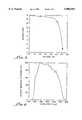
- FIG. 3is the current vs. voltage performance plot of a CdS/CuInSe 2 solar cell prepared according to Example 3 of the present invention.
- FIG. 4is a plot of relative quantum efficiency verses wavelength for the CdS/CuInSe 2 solar cell of Example 3.
- the present inventionincludes an essentially two-step process for fabricating high quality, low cost thin film CIGS semiconductor devices that exhibit photovoltaic characteristics and are especially adaptable for solar cell applications.
- This first stepmay include a unique process and electrodeposition bath for electrodepositing gallium concurrently with other elements, as well as the unique use of an alternating current in conjunction with a direct current.
- the second stepis physical vapor deposition of either Cu+Se or In+Se, either alone or in combination with Ga.
- this second stepthe composition of the overall film is carefully controlled so that the resulting thin film is very close to stoichiometric Cu(In,Ga)Se 2 .
- Both of these stepsmay be performed on substrates having large surface areas. Accordingly, the process of the present invention allows large area, high efficiency solar cells to be economically produced.
- CdS/CIGS photovoltaic device 10includes a substrate 12 which may be, for example, soda-lime silica glass or amorphous 7059 glass.
- Substrate 12further includes a back contact layer 14 of molybdenum, about 1-2 ⁇ m thick.
- the molybdenummay be deposited using DC sputtering from a rotating cylindrical magnetron target (CMAG).
- CMAGrotating cylindrical magnetron target
- an additional adhesion layer 16 of coppermay also be deposited as by electrodeposition.
- the substrateshould be degreased as for example with propanol and dried in flowing nitrogen gas.
- a precursor film 18is then deposited by electrodeposition.
- the precursor filmcontains one or more of the elements copper, indium, gallium, and selenium.
- Electrodepositionis generally a less expensive method of depositing these materials than vapor deposition. However, it is not possible to control the ratios of metals deposited during electrodeposition as precisely as desired. Consequently, prior CIGS layers deposited entirely by electrodeposition produced low conversion efficiencies.
- the electrodeposition stepis integrated with the vapor deposition step that follows. This allows precursor material to be deposited in bulk using an economical electrodeposition step, followed by a vapor deposition step to carefully control the final elemental ratios. This results in economical production yet high efficiencies of the resulting cell.
- the precursor film 18should be deposited to about 1-3 ⁇ m thick, with thickness being controlled by coulometric measurements.
- the plating solutionis adjusted to have a pH of approximately 1.0 to 4.0, and more preferably to about 1.4 to 2.4.
- the plating solutionshould preferably be at about 10° C. to 80° C., and more preferably at about 24° C.
- Adding a supporting electrolyte to the plating bathcan additionally increase the conductivity of the plating solution, allowing for a further increase in the electrodeposition rate.
- Saltssuch as NaCl, LiCl, or Na 2 SO 4 have been found to be suitable supporting electrolytes for use with certain embodiments of the present invention.
- the water in the plating solutionmay be either partially or completely replaced by one or more organic solvents such as dimethyl sulfoxide (DMSO).
- DMSOdimethyl sulfoxide
- Increasing the organic solvent content of the electrodeposition solutionallows the cathodic potential to be increased without unacceptable increases in metal oxide and hydroxide formation rates.
- the increased cathodic potentialincreases the deposition rate of the precursor films.
- An additional advantageis that increasing the cathodic potential increases the deposition rate of gallium relative to the deposition rates of other deposited metals.
- the cathodic potentialallows the cathodic potential to be selected from a wider range so as to achieve a more desired stoichiometry of the as-deposited precursor film 18.
- the preferred cathodic potentialis approximately 3-10 VDC and 0.2-5.0 VAC at approximately 1-100 KHz. Value of approximately 5 VDC and 0.45 VAC at approximately 18.1 KHz were found to yield good results.
- a second electroplating solutionmay be employed to adjust the stoichiometry of the electrodeposited film prior to the vapor deposition phase.
- a first electrodeposition stepmay produce a CIGS precursor film with less gallium than optimally desired.
- gallium contentcan be increased during the vapor deposition phase, it may be less expensive to deposit a certain amount of gallium using a second electrodeposition solution to make a coarse stoichiometric adjustment prior to proceeding to fine stoichiometric adjustment at the vapor deposition step.
- Another potential motivation for using a second electrodeposition solutionis to achieve a composition gradient in the deposited film, as suggested by U.S. Pat. No. 4,335,266 issued to Michelsen et al.
- composition-graded CIGS thin films for solar cell and other applicationswhich is hereby incorporated by reference for its teachings of composition-graded CIGS thin films for solar cell and other applications.
- Yet another way of achieving composition grading during electrodepositionis to vary process parameters such as cathodic potential, ionic concentrations, pH, or temperature, as electrodeposition proceeds.
- electrodeposited precursor films fabricated according to the present inventioninclude In--Se, Cu--Se, and Cu--In--Se precursor films.
- Gashould be added to raise the energy gap.
- the Gamay be added by a separate electrodeposition step, though is preferably added at the vapor deposition step by vaporizing elemental gallium.
- An exampleis also given of a novel solution and process that allows Ga to be electrodeposited along with other precursor metals, to produce a Cu--In--Ga--Se precursor film electrodeposited in a single step.
- the solutionincludes ions of each of the elements of copper, indium, gallium, and selenium. These ions may be supplied in the form of dissolved metal salts.
- the substrate (precursor film) temperatureshould be 300° C. to 600° C. during PVD, and preferably about 550° C.
- the filmsshould then be annealed. Annealing improves the homogeneity and quality of the films.
- a high quality CIGS filmis one that does not exhibit an excessive amount of copper nodules, voids, or vacancies in the film which would reduce conversion efficiencies.
- Annealing the films at 250° C. to 500° C. in a vacuum, followed by slow cooling at a rate of approximately 3° C./min to avoid thermal shockwas found to yield good results.
- seleniumhas a much higher vapor pressure than either copper, indium, or gallium, selenium may be lost from the film during the high temperature steps of vapor deposition and annealing. To compensate, the atmosphere during these steps may contain a moderate overpressure of selenium.
- the filmis selenized at a rate of 5-100 ⁇ /s during cool-down from PVD temperature to annealing temperature.
- CdS layer 22is preferably deposited by chemical bath deposition (CBD) to a thickness of approximately 200-1000 ⁇ .
- CBD bathmay be prepared from 0.08 gm CdSO 4 , 2.5 gm thiourea, and 27.5 gm NH 4 OH dissolved in 200 ml water.
- the deposition temperatureshould be approximately 40°-80° C.
- a layer 28 of conducting wide bandgap n-type semiconductor materialsis deposited next.
- layer 28comprises two zinc oxide layers 24 and 26 as shown in FIG. 2.
- First zinc oxide layer 24is deposited with RF sputtering at approximately 0.62 watts/cm 2 in an argon plasma at 10 millitorrs pressure.
- Second zinc oxide layer 26,comprising approximately 1-5% Al 2 O 3 -doped zinc oxide, is also prepared using RF sputtering at approximately 1.45 watts/cm 2 in an argon plasma at 10 millitorrs pressure.
- the resistivity of the first layerwas 50-200 ohm/cm 2
- resistivity of the second layerwas 15-20 ohm/cm 2 .
- the transmissivity of the overall ZnO layerwas 80-85%.
- Bi-layer metal contacts 30may then be prepared with an e-beam system or other techniques.
- a first metal contact layerwas 500-1000 ⁇ thick Ni and the second metal contact layer was 1-3 ⁇ m thick Al.
- Metal contacts 30will generally be laid out in fine grid lines across the collecting surface of the device and connected to a suitable current collecting electrode (not shown).
- the efficiency of the resulting devicecan be further increased by adding an antireflection coating 32, such as a 600-1000 ⁇ layer of MgF 2 by electron beam.
- a device prepared according to Example 3 belowexhibited a conversion efficiency of 9.44%.
- a precursor film of In 1-2 Se 1-3was electrodeposited on glass substrates coated with a Mo or Mo/Cu layer approximately 500 ⁇ thick.
- the precursor filmwas deposited using an electroplating solution containing 2.25 gm InCl 3 and 0.41 gm H 2 SeO 3 dissolved in 200 ml of water. The pH of the solution was adjusted between 1.4 and 2.4 using dilute HCl (10% by volume).
- the filmswere deposited by applying a 2-5 V direct current voltage in combination with an alternating current voltage of 0.45 V at 18.1 KHz frequency. The films were 1-3 ⁇ m thick and adhered to the substrate.
- a precursor film of Cu 1-2 Se 1-3was electrodeposited on a substrate using an electroplating solution containing 6.21 gm Cu(NO 3 ) 2 ⁇ 6H 2 O and 1.16 gm H 2 SeO 3 dissolved in 300 ml water. The pH was adjusted between 1.4 and 2.4 using dilute HCl (10% by volume). The films were deposited by applying a 2-5 V direct current voltage in combination with an alternating current voltage of 0.45 V at 18.1 KHz frequency. As deposited layers were 1-3 ⁇ m thick and adhered to the substrate.
- a precursor film of Cu 1-2 In 1-2 Se 1-3was electrodeposited on a substrate using an electroplating solution containing 4.47 gm CuCl 2 , 5.67 gm InCl 3 and 3.39 gm H 2 SeSO 3 dissolved in 1050 ml water. The pH was adjusted between 1.4 and 2.4 using dilute HCl (10% by volume). The films were deposited by applying a 2-5 V direct current voltage in combination with an alternating current voltage of 0.45 V at 18.1 KHz frequency. As deposited layers were 1-3 ⁇ m thick and adhered to the substrate. The electrodeposited film was slightly indium poor. Indium was then added by vapor deposition to adjust the final content to approximately CuInSe 2 . CdS and ZnO were then added to complete the solar cell. The resulting solar cell was exposed to ASTM E892-87 Global (1000 Wm -2 ) standard irradiance spectrum at 25° C. Performance parameters for the finished solar cell, having an area of 0.4285 cm 2 , were measured as:
- FIG. 3is an I-V plot for the device.
- FIG. 4is a plot of the relative quantum efficiency of the device.
- the devicecontained only Cu--In--Se, without any gallium.
- the deviceexhibited an efficiency of 8.76% without antireflective coating, and 9.44% after an antireflective coating was added. It is believed that by adding gallium the efficiency of the resulting cell could be improved to around fourteen percent (14%).
- a precursor film of Cu 1-2 In 1-2 Ga 0 .01-1 Se 1-3was electrodeposited using a solution containing 1.12 gm Cu(NO 3 ) 2 ⁇ 6H 2 O, 12.0 gm InCl 3 , 4.60 gm Ga(NO 3 ) 3 ⁇ xH 2 O and 1.80 gm H 2 SeO 3 dissolved in 450 ml of water.
- a precursor film of Cu 1-2 In 1-2 Ga 0 .01-1 Se 1-3was electrodeposited using a solution containing 1.496 gm Cu(No 3 ) ⁇ 5H 2 O, 14.929 gm InCl 3 , 1.523 gm H 2 SeO 3 , and 7.192 gm Ga(NO 3 ) 3 dissolved in 450 ml of DMSO.
- the filmswere deposited at 25° C. and also at 50° C. at an applied voltage of 5 VDC.
- a precursor film of Cu 1-2 In 1-2 Ga 0 .01-1 Se 1-3was electrodeposited using a solution containing 1.496 gm Cu(No 3 ) ⁇ 5H 2 O, 14.929 gm InCl 3 , 1.523 gm H 2 SeO 3 , and 7.192 gm Ga(NO 3 ) 3 dissolved in a mixture of 400 ml DMSO and 50 ml water.
- the filmswere deposited at 25° C. and also at 50° C. at an applied voltage of 5 VDC.
- a precursor film of Cu 1-2 In 1-2 Ga 0 .01-1 Se 1-3was electrodeposited using a solution containing 1.496 gm Cu(No 3 ) ⁇ 5H 2 O, 14.929 gm InCl 3 , 1.523 gm H 2 SeO 3 , 7.192 gm Ga(NO 3 ) 3 , and 10 gm Na 2 SO 4 , and 20 gm LiCl dissolved in a mixture of 400 ml DMSO and 50 ml water.
- the filmswere deposited at 25° C. and also at 50° C. at an applied voltage of 5 VDC.
- the present invention as described abovemay be incorporated in a variety of applications, as for example the conversion of solar energy to electric energy for baseline power generation.
- Other applicationsinclude appliances such as solar-powered calculators, battery charges such as those used with freeway emergency call boxes, photoelectric eyes, night security light activators, light meters for photographic and other purposes, and the like.
Landscapes
- Engineering & Computer Science (AREA)
- Chemical & Material Sciences (AREA)
- Physics & Mathematics (AREA)
- General Physics & Mathematics (AREA)
- Materials Engineering (AREA)
- Microelectronics & Electronic Packaging (AREA)
- Condensed Matter Physics & Semiconductors (AREA)
- Manufacturing & Machinery (AREA)
- Computer Hardware Design (AREA)
- Power Engineering (AREA)
- Chemical Kinetics & Catalysis (AREA)
- Metallurgy (AREA)
- Organic Chemistry (AREA)
- Electrochemistry (AREA)
- Spectroscopy & Molecular Physics (AREA)
- Mechanical Engineering (AREA)
- Photovoltaic Devices (AREA)
- Physical Vapour Deposition (AREA)
- Electroplating And Plating Baths Therefor (AREA)
- Electroplating Methods And Accessories (AREA)
- Conductive Materials (AREA)
Abstract
Description
This application is a divisional of U.S. application Ser. No. 08/571,150, filed Dec. 12, 1995, now U.S. Pat. No. 5,730,852 which is a continuation-in-part of provisional application Ser. No. 60/004,269, filed Sep. 25, 1995.
1. Field of the Invention
The field of the present invention relates to the preparation of thin film semiconductor devices. More particularly, the present invention relates to electrodeposition of copper-indium-gallium-selenide films for solar cells.
2. Description of the Related Art
Chalcopyrite ternary thin films of copper-indium-diselenide (CuInSe2) and copper-indium-gallium-diselenide (CuIn1-x Gax Se2), both of which are generically referred to as Cu(In,Ga)Se2, CIGS, or simply CIS, have become the subject of considerable interest and study for semiconductor devices in recent years. Sulphur can also be, and sometimes is, substituted for selenium, so the compound is sometimes also referred to even more generically as Cu(In,Ga)(Se,S)2 so as to encompass all of these possible combinations. These devices are also referred to as I-III-VI2 devices according to their constituent elemental groups.
These devices are of particular interest for photovoltaic device or solar cell absorber applications. For photovoltaic applications, the p-type CIGS layer is combined with an n-type CdS layer to form a p-n heterojunction CdS/CIGS device. The direct energy gap of CIGS results in a large optical absorption coefficient, which in turn permits the use of thin layers on the order of 1-2 μm. An additional advantage of CIGS devices is their long-term stability.
Various methods have been reported for fabricating CIGS thin films. Some of the earliest techniques involved heating copper and indium on a substrate in the presence of a selenium-containing gas, including H2 Se. The heating of copper and indium films in the presence of a selenium-containing gas is known as selenization. One drawback to selenizing with H2 Se is that H2 Se gas is highly toxic, thus presenting serious hazards to humans in large scale production environments.
In U.S. Pat. No. 5,045,409, Eberspacher et al. disclose depositing copper and indium films by magnetron sputtering, and depositing a selenium film by thermal evaporation, followed by heating in the presence of various gases. Other methods for producing CIS films have included Molecular Beam Epitaxy, electrodeposition either in single or multiple steps, and vapor deposition of single crystal and polycrystalline films.
Although vapor deposition techniques have been used to yield solar cells with efficiencies as high as seventeen percent (17%), vapor deposition is costly. Accordingly, solar cells made by vapor deposition have generally been limited to devices for laboratory experimentation, and are not suitable for large scale production. On the other hand, thin film solar cells made by electrodeposition techniques are generally much less expensive. However, solar cells produced by electrodeposition generally suffer from low efficiencies. For example, in Solar Cells with Improved Efficiency Based on Electrodeposited Copper Indium Diselenide Thin Films, ADVANCED MATERIALS, Vol. 6 No. 5 (1994), Guillemoles et al. report solar cells prepared by electrodeposition with efficiencies on the order of 5.6%.
Accordingly, it is a general object of this invention to provide an improved process for fabricating high quality thin film Cu(In,Ga)Se2 solar cells.
It is also an object of this invention to provide low cost, high quality thin film solar cells having high conversion efficiencies.
It is a further object of this invention to provide a process for producing Cu--In, Cu--Se, Cu--In--Se, and Cu--In--Ga--Se thin films that have applications in solar and non-solar cells.
It is a still further object of this invention to provide a process for electrodepositing a gallium-containing thin-film solar cell precursor.
To achieve the foregoing and other objects and advantages in accordance with the purpose of the present invention, as embodied and broadly described herein, the process of this invention includes electrodepositing a layer of Cux Iny Gaz Sen (x=0-2, y=0-2, z=0-2, n=0-3), preferably using direct current in combination with alternating current, followed by vapor depositing additional copper and selenium or indium and selenium to adjust the final composition very close to stoichiometric Cu(In,Ga)Se2. This unique two-step film deposition process allows precursor films to be deposited by inexpensive electrodeposition, and then adjusted using the more expensive but more precise technique of physical vapor deposition to bring the final film into the desired stoichiometric range. Solar cells may then be completed as for example by chemical bath deposition (CBD) of CdS followed by sputtering of ZnO, and addition of bi-layer metal contacts as well as optional anti-reflective coating. A solar cell made according to the present process has exhibited a device efficiency of 9.44%.
Additional objects, advantages, and novel features of the present invention will be set forth in part in the description that follows, and in part will become apparent to those skilled in the art upon examination of the following description and drawings.
FIG. 1 is a cross sectional view of a CIGS photovoltaic device prepared according to the present invention.
FIG. 2 is a cross sectional view of the conductingzinc oxide layer 28 shown in FIG. 1.
FIG. 3 is the current vs. voltage performance plot of a CdS/CuInSe2 solar cell prepared according to Example 3 of the present invention.
FIG. 4 is a plot of relative quantum efficiency verses wavelength for the CdS/CuInSe2 solar cell of Example 3.
The present invention includes an essentially two-step process for fabricating high quality, low cost thin film CIGS semiconductor devices that exhibit photovoltaic characteristics and are especially adaptable for solar cell applications. In the first step, a precursor film of Cux Iny Gaz Sen (x=0-2, y=0-2, z=0-2, n=0-3) is electrodeposited on a substrate such as glass coated with molybdenum. This first step may include a unique process and electrodeposition bath for electrodepositing gallium concurrently with other elements, as well as the unique use of an alternating current in conjunction with a direct current.
The second step is physical vapor deposition of either Cu+Se or In+Se, either alone or in combination with Ga. In this second step the composition of the overall film is carefully controlled so that the resulting thin film is very close to stoichiometric Cu(In,Ga)Se2. Both of these steps may be performed on substrates having large surface areas. Accordingly, the process of the present invention allows large area, high efficiency solar cells to be economically produced.
Referring now to FIG. 1, CdS/CIGSphotovoltaic device 10 includes asubstrate 12 which may be, for example, soda-lime silica glass or amorphous 7059 glass.Substrate 12 further includes aback contact layer 14 of molybdenum, about 1-2 μm thick. The molybdenum may be deposited using DC sputtering from a rotating cylindrical magnetron target (CMAG). To improve adhesion between theMo layer 14 and the precursor film to be deposited, anadditional adhesion layer 16 of copper may also be deposited as by electrodeposition. AfterMo layer 14 and optionalcopper adhesion layer 16 have been deposited, the substrate should be degreased as for example with propanol and dried in flowing nitrogen gas.
Aprecursor film 18 is then deposited by electrodeposition. The precursor film contains one or more of the elements copper, indium, gallium, and selenium. Electrodeposition is generally a less expensive method of depositing these materials than vapor deposition. However, it is not possible to control the ratios of metals deposited during electrodeposition as precisely as desired. Consequently, prior CIGS layers deposited entirely by electrodeposition produced low conversion efficiencies. In the present invention, the electrodeposition step is integrated with the vapor deposition step that follows. This allows precursor material to be deposited in bulk using an economical electrodeposition step, followed by a vapor deposition step to carefully control the final elemental ratios. This results in economical production yet high efficiencies of the resulting cell. The composition ofprecursor film 18 is generally denoted as Cux Iny Gaz Sen (x=0-2, y=0-2, z=0-2, n=0-3). Theprecursor film 18 should be deposited to about 1-3 μm thick, with thickness being controlled by coulometric measurements.
It has been found that electrodepositing the films using an AC voltage in addition to a DC voltage produces improved results. An AC voltage improves the morphology of the film. It is also believed that the AC voltage improves nucleation (growth) of the thin film by allowing additional nucleation centers to be created. For an entirely aqueous plating solution, the applicable DC voltage range is approximately 1-5 VDC, with a preferred voltage of approximately 2 VDC. Improved results may be obtained by superimposing an AC voltage of 0.2-5.0 VAC at 1-100 Khz, with preferred values of approximately 0.3-1.0 VAC at 10-30 KHz. A value of approximately 0.45 VAC at approximately 18.1 KHz was found to yield good results. The plating solution is adjusted to have a pH of approximately 1.0 to 4.0, and more preferably to about 1.4 to 2.4. The plating solution should preferably be at about 10° C. to 80° C., and more preferably at about 24° C. Adding a supporting electrolyte to the plating bath can additionally increase the conductivity of the plating solution, allowing for a further increase in the electrodeposition rate. Salts such as NaCl, LiCl, or Na2 SO4 have been found to be suitable supporting electrolytes for use with certain embodiments of the present invention.
In completely aqueous solutions, electrolysis of water molecules begins to occur to an undesirable extent at approximately 2-3 volts. The resulting O2- and OH- ions combine with deposition metal ions or deposited metal to form unwanted metal oxides and hydroxides on theprecursor film 18. To overcome this disadvantage, the water in the plating solution may be either partially or completely replaced by one or more organic solvents such as dimethyl sulfoxide (DMSO). Increasing the organic solvent content of the electrodeposition solution allows the cathodic potential to be increased without unacceptable increases in metal oxide and hydroxide formation rates. The increased cathodic potential increases the deposition rate of the precursor films. An additional advantage is that increasing the cathodic potential increases the deposition rate of gallium relative to the deposition rates of other deposited metals. Therefore, using a solution containing one or more organic solvents allows the cathodic potential to be selected from a wider range so as to achieve a more desired stoichiometry of the as-depositedprecursor film 18. When an organic solvent is used, the preferred cathodic potential is approximately 3-10 VDC and 0.2-5.0 VAC at approximately 1-100 KHz. Value of approximately 5 VDC and 0.45 VAC at approximately 18.1 KHz were found to yield good results.
If desired, a second electroplating solution may be employed to adjust the stoichiometry of the electrodeposited film prior to the vapor deposition phase. For example, a first electrodeposition step may produce a CIGS precursor film with less gallium than optimally desired. Although the gallium content can be increased during the vapor deposition phase, it may be less expensive to deposit a certain amount of gallium using a second electrodeposition solution to make a coarse stoichiometric adjustment prior to proceeding to fine stoichiometric adjustment at the vapor deposition step. Another potential motivation for using a second electrodeposition solution is to achieve a composition gradient in the deposited film, as suggested by U.S. Pat. No. 4,335,266 issued to Michelsen et al. which is hereby incorporated by reference for its teachings of composition-graded CIGS thin films for solar cell and other applications. Yet another way of achieving composition grading during electrodeposition is to vary process parameters such as cathodic potential, ionic concentrations, pH, or temperature, as electrodeposition proceeds.
Several examples of electrodeposited precursor films fabricated according to the present invention are given. These examples include In--Se, Cu--Se, and Cu--In--Se precursor films. For these precursor films, Ga should be added to raise the energy gap. The Ga may be added by a separate electrodeposition step, though is preferably added at the vapor deposition step by vaporizing elemental gallium. An example is also given of a novel solution and process that allows Ga to be electrodeposited along with other precursor metals, to produce a Cu--In--Ga--Se precursor film electrodeposited in a single step. The solution includes ions of each of the elements of copper, indium, gallium, and selenium. These ions may be supplied in the form of dissolved metal salts.
After theprecursor film 18 has been electrodeposited it should be cleaned. A suitable method is to rinseprecursor film 18 with deionized water and dry it in flowing nitrogen gas. Afterprecursor film 18 has been cleaned, anadditional layer 20 of In+Se or Cu+Se, either alone or in combination with gallium, is deposited by physical vapor deposition to adjust the final film composition to the ratios of approximately Cu=1-1.2:(In,Ga)=1-1.2:Se=2-2.5, and most preferably to approximately 1:1:2. By controlling the ratio of In/Ga the energy gap between the CdS and the CIGS layers can be adjusted to the optimal or nearly optimal value. An energy gap of approximately 1.45 eV is considered optimal for terrestrial solar energy conversion, and is achieved by an In/Ga ratio of approximately 3:1. The substrate (precursor film) temperature should be 300° C. to 600° C. during PVD, and preferably about 550° C.
After PVD, the films should then be annealed. Annealing improves the homogeneity and quality of the films. A high quality CIGS film is one that does not exhibit an excessive amount of copper nodules, voids, or vacancies in the film which would reduce conversion efficiencies. Annealing the films at 250° C. to 500° C. in a vacuum, followed by slow cooling at a rate of approximately 3° C./min to avoid thermal shock was found to yield good results. Because selenium has a much higher vapor pressure than either copper, indium, or gallium, selenium may be lost from the film during the high temperature steps of vapor deposition and annealing. To compensate, the atmosphere during these steps may contain a moderate overpressure of selenium. In the preferred embodiment, the film is selenized at a rate of 5-100 Å/s during cool-down from PVD temperature to annealing temperature.
Once the CIGS layers 18 and 20 collectively are deposited and annealed, athin layer 22 of n-type semiconductor comprising cadmium sulfide is deposited next.CdS layer 22 is preferably deposited by chemical bath deposition (CBD) to a thickness of approximately 200-1000 Å. The CBD bath may be prepared from 0.08 gm CdSO4, 2.5 gm thiourea, and 27.5 gm NH4 OH dissolved in 200 ml water. The deposition temperature should be approximately 40°-80° C.
Alayer 28 of conducting wide bandgap n-type semiconductor materials is deposited next. In the preferred embodiment,layer 28 comprises two zinc oxide layers 24 and 26 as shown in FIG. 2. Firstzinc oxide layer 24 is deposited with RF sputtering at approximately 0.62 watts/cm2 in an argon plasma at 10 millitorrs pressure. Secondzinc oxide layer 26, comprising approximately 1-5% Al2 O3 -doped zinc oxide, is also prepared using RF sputtering at approximately 1.45 watts/cm2 in an argon plasma at 10 millitorrs pressure. In an exemplary embodiment the resistivity of the first layer was 50-200 ohm/cm2, and resistivity of the second layer was 15-20 ohm/cm2. The transmissivity of the overall ZnO layer was 80-85%.
A precursor film of In1-2 Se1-3 was electrodeposited on glass substrates coated with a Mo or Mo/Cu layer approximately 500 Å thick. The precursor film was deposited using an electroplating solution containing 2.25 gm InCl3 and 0.41 gm H2 SeO3 dissolved in 200 ml of water. The pH of the solution was adjusted between 1.4 and 2.4 using dilute HCl (10% by volume). The films were deposited by applying a 2-5 V direct current voltage in combination with an alternating current voltage of 0.45 V at 18.1 KHz frequency. The films were 1-3 μm thick and adhered to the substrate.
A precursor film of Cu1-2 Se1-3 was electrodeposited on a substrate using an electroplating solution containing 6.21 gm Cu(NO3)2 ·6H2 O and 1.16 gm H2 SeO3 dissolved in 300 ml water. The pH was adjusted between 1.4 and 2.4 using dilute HCl (10% by volume). The films were deposited by applying a 2-5 V direct current voltage in combination with an alternating current voltage of 0.45 V at 18.1 KHz frequency. As deposited layers were 1-3 μm thick and adhered to the substrate.
A precursor film of Cu1-2 In1-2 Se1-3 was electrodeposited on a substrate using an electroplating solution containing 4.47 gm CuCl2, 5.67 gm InCl3 and 3.39 gm H2 SeSO3 dissolved in 1050 ml water. The pH was adjusted between 1.4 and 2.4 using dilute HCl (10% by volume). The films were deposited by applying a 2-5 V direct current voltage in combination with an alternating current voltage of 0.45 V at 18.1 KHz frequency. As deposited layers were 1-3 μm thick and adhered to the substrate. The electrodeposited film was slightly indium poor. Indium was then added by vapor deposition to adjust the final content to approximately CuInSe2. CdS and ZnO were then added to complete the solar cell. The resulting solar cell was exposed to ASTM E892-87 Global (1000 Wm-2) standard irradiance spectrum at 25° C. Performance parameters for the finished solar cell, having an area of 0.4285 cm2, were measured as:
______________________________________ V.sub.oc = 0.4138 V V.sub.Pmax = 0.3121 V I.sub.sc = 15.40 mA I.sub.Pmax = 12.96 mA J.sub.sc = 35.94 mA cm.sup.-2 P.sub.max = 4.045 mW Fill Factor = 63.47% Efficiency = 9.44% ______________________________________
FIG. 3 is an I-V plot for the device. FIG. 4 is a plot of the relative quantum efficiency of the device. The device contained only Cu--In--Se, without any gallium. The device exhibited an efficiency of 8.76% without antireflective coating, and 9.44% after an antireflective coating was added. It is believed that by adding gallium the efficiency of the resulting cell could be improved to around fourteen percent (14%).
A precursor film of Cu1-2 In1-2 Ga0.01-1 Se1-3 was electrodeposited using a solution containing 1.12 gm Cu(NO3)2 ·6H2 O, 12.0 gm InCl3, 4.60 gm Ga(NO3)3 ·xH2 O and 1.80 gm H2 SeO3 dissolved in 450 ml of water. This is equivalent to approximately 2.49 gm/l Cu(NO3)2 ·6H2 O, 26.7 gm/l InCl3, 10.2 gm/l Ga(NO3)3 ·xH2 O and 4.0 gm/l H2 SeO3, and approximately 0.0084, 0.12, 0.28, and 0.31 molar of copper, indium, gallium, and selenium ions, respectively. The pH was adjusted between 1.4 and 2.4 using dilute HCl (10% by volume). The films were deposited by applying a 2-5 V direct current voltage in combination with an alternating current voltage of 0.45 V at 18.1 KHz frequency. As deposited layers were 1-3 μm thick and adhered to the substrate.
A precursor film of Cu1-2 In1-2 Ga0.01-1 Se1-3 was electrodeposited using a solution containing 1.496 gm Cu(No3)·5H2 O, 14.929 gm InCl3, 1.523 gm H2 SeO3, and 7.192 gm Ga(NO3)3 dissolved in 450 ml of DMSO. The films were deposited at 25° C. and also at 50° C. at an applied voltage of 5 VDC.
A precursor film of Cu1-2 In1-2 Ga0.01-1 Se1-3 was electrodeposited using a solution containing 1.496 gm Cu(No3)·5H2 O, 14.929 gm InCl3, 1.523 gm H2 SeO3, and 7.192 gm Ga(NO3)3 dissolved in a mixture of 400 ml DMSO and 50 ml water. The films were deposited at 25° C. and also at 50° C. at an applied voltage of 5 VDC.
A precursor film of Cu1-2 In1-2 Ga0.01-1 Se1-3 was electrodeposited using a solution containing 1.496 gm Cu(No3)·5H2 O, 14.929 gm InCl3, 1.523 gm H2 SeO3, 7.192 gm Ga(NO3)3, and 10 gm Na2 SO4, and 20 gm LiCl dissolved in a mixture of 400 ml DMSO and 50 ml water. The films were deposited at 25° C. and also at 50° C. at an applied voltage of 5 VDC.
The present invention as described above may be incorporated in a variety of applications, as for example the conversion of solar energy to electric energy for baseline power generation. Other applications include appliances such as solar-powered calculators, battery charges such as those used with freeway emergency call boxes, photoelectric eyes, night security light activators, light meters for photographic and other purposes, and the like.
Although the present invention has thus been described in detail with regard to the preferred embodiments and drawings and examples thereof, it should be apparent to those skilled in the art that various adaptations and modifications of the present invention may be accomplished without departing from the spirit and the scope of the invention. Accordingly, it is to be understood that the detailed description and the accompanying drawings as set forth hereinabove are not intended to limit the breadth of the present invention, which should be inferred only from the following claims and their appropriately construed legal equivalents.
Claims (8)
1. A process for electrodepositing a solar cell precursor thin film, the process comprising the steps of:
electrodepositing a thin film containing copper, indium, gallium, and selenium onto a substrate, the electrodeposition proceeding in an electrodeposition solution comprising copper, indium, gallium, and selenium ions.
2. The process of claim 1, wherein said electrodeposition solution comprises copper, indium, gallium, and selenium ions at concentrations of approximately 0.0084, 0.12, 0.28, and 0.31 molar, respectively.
3. The process of claim 2, wherein said electrodeposition solution comprises approximately 2.49 gm/l Cu(NO3)2 ·6H2 O, 26.7 gm/l InCl3, 10.2 gm/l Ga(NO3)3, and 4.0 gm/l (H2 SeO3).
4. The process of claim 1, wherein the electrodeposition solution has a pH of approximately 1.0-4.0.
5. The process of claim 1 wherein the electrodeposition proceeds at a DC voltage of 1-10 V.
6. The process of claim 5 wherein the electrodeposition proceeds at a superimposed AC voltage of approximately 0.2-5.0 V at a frequency of approximately 1-100 KHz.
7. The process of claim 6 wherein said superimposed AC voltage is approximately 0.45 VAC at a frequency of approximately 18.1 KHz.
8. The process of claim 1 wherein the electrodeposition solution further comprises at least one organic solvent, and the electrodeposition proceeds at a DC voltage of approximately 3-10 volts.
Priority Applications (1)
| Application Number | Priority Date | Filing Date | Title |
|---|---|---|---|
| US08/979,358US5804054A (en) | 1995-12-12 | 1997-11-26 | Preparation of copper indium gallium diselenide films for solar cells |
Applications Claiming Priority (2)
| Application Number | Priority Date | Filing Date | Title |
|---|---|---|---|
| US08/571,150US5730852A (en) | 1995-09-25 | 1995-12-12 | Preparation of cuxinygazsen (X=0-2, Y=0-2, Z=0-2, N=0-3) precursor films by electrodeposition for fabricating high efficiency solar cells |
| US08/979,358US5804054A (en) | 1995-12-12 | 1997-11-26 | Preparation of copper indium gallium diselenide films for solar cells |
Related Parent Applications (1)
| Application Number | Title | Priority Date | Filing Date |
|---|---|---|---|
| US08/571,150DivisionUS5730852A (en) | 1995-09-25 | 1995-12-12 | Preparation of cuxinygazsen (X=0-2, Y=0-2, Z=0-2, N=0-3) precursor films by electrodeposition for fabricating high efficiency solar cells |
Publications (1)
| Publication Number | Publication Date |
|---|---|
| US5804054Atrue US5804054A (en) | 1998-09-08 |
Family
ID=24282508
Family Applications (3)
| Application Number | Title | Priority Date | Filing Date |
|---|---|---|---|
| US08/571,150Expired - LifetimeUS5730852A (en) | 1995-09-25 | 1995-12-12 | Preparation of cuxinygazsen (X=0-2, Y=0-2, Z=0-2, N=0-3) precursor films by electrodeposition for fabricating high efficiency solar cells |
| US08/870,081Expired - LifetimeUS5871630A (en) | 1995-12-12 | 1997-06-05 | Preparation of copper-indium-gallium-diselenide precursor films by electrodeposition for fabricating high efficiency solar cells |
| US08/979,358Expired - LifetimeUS5804054A (en) | 1995-12-12 | 1997-11-26 | Preparation of copper indium gallium diselenide films for solar cells |
Family Applications Before (2)
| Application Number | Title | Priority Date | Filing Date |
|---|---|---|---|
| US08/571,150Expired - LifetimeUS5730852A (en) | 1995-09-25 | 1995-12-12 | Preparation of cuxinygazsen (X=0-2, Y=0-2, Z=0-2, N=0-3) precursor films by electrodeposition for fabricating high efficiency solar cells |
| US08/870,081Expired - LifetimeUS5871630A (en) | 1995-12-12 | 1997-06-05 | Preparation of copper-indium-gallium-diselenide precursor films by electrodeposition for fabricating high efficiency solar cells |
Country Status (13)
| Country | Link |
|---|---|
| US (3) | US5730852A (en) |
| EP (1) | EP0956600B1 (en) |
| JP (1) | JP3753739B2 (en) |
| KR (1) | KR19990071500A (en) |
| CN (1) | CN1155111C (en) |
| AU (1) | AU705545B2 (en) |
| BR (1) | BR9612022A (en) |
| CA (1) | CA2239786C (en) |
| DE (1) | DE69621467T2 (en) |
| IL (1) | IL124750A0 (en) |
| NO (2) | NO320118B1 (en) |
| SA (1) | SA98190373B1 (en) |
| WO (1) | WO1997022152A1 (en) |
Cited By (40)
| Publication number | Priority date | Publication date | Assignee | Title |
|---|---|---|---|---|
| US6258620B1 (en)* | 1997-10-15 | 2001-07-10 | University Of South Florida | Method of manufacturing CIGS photovoltaic devices |
| US6409907B1 (en)* | 1999-02-11 | 2002-06-25 | Lucent Technologies Inc. | Electrochemical process for fabricating article exhibiting substantial three-dimensional order and resultant article |
| US20040206390A1 (en)* | 2000-04-10 | 2004-10-21 | Bhattacharya Raghu Nath | Preparation of CIGS-based solar cells using a buffered electrodeposition bath |
| US20050072461A1 (en)* | 2003-05-27 | 2005-04-07 | Frank Kuchinski | Pinhole porosity free insulating films on flexible metallic substrates for thin film applications |
| US20050202589A1 (en)* | 2004-03-15 | 2005-09-15 | Basol Bulent M. | Technique and apparatus for depositing thin layers of semiconductors for solar cell fabrication |
| US20060121701A1 (en)* | 2004-03-15 | 2006-06-08 | Solopower, Inc. | Technique and apparatus for depositing layers of semiconductors for solar cell and module fabrication |
| US20070093006A1 (en)* | 2005-10-24 | 2007-04-26 | Basol Bulent M | Technique For Preparing Precursor Films And Compound Layers For Thin Film Solar Cell Fabrication And Apparatus Corresponding Thereto |
| US20070116892A1 (en)* | 2005-11-18 | 2007-05-24 | Daystar Technologies, Inc. | Methods and apparatus for treating a work piece with a vaporous element |
| US20070145507A1 (en)* | 2005-11-02 | 2007-06-28 | Basol Bulent M | Contact Layers For Thin Film Solar Cells Employing Group IBIIIAVIA Compound Absorbers |
| US20070166964A1 (en)* | 2005-03-15 | 2007-07-19 | Basol Bulent M | Precursor Containing Copper Indium And Gallium For Selenide (Sulfide) Compound Formation |
| US20070169809A1 (en)* | 2004-02-19 | 2007-07-26 | Nanosolar, Inc. | High-throughput printing of semiconductor precursor layer by use of low-melting chalcogenides |
| US20070227633A1 (en)* | 2006-04-04 | 2007-10-04 | Basol Bulent M | Composition control for roll-to-roll processed photovoltaic films |
| WO2007120776A2 (en) | 2006-04-14 | 2007-10-25 | Silica Tech, Llc | Plasma deposition apparatus and method for making solar cells |
| US20070272558A1 (en)* | 2006-01-06 | 2007-11-29 | Serdar Aksu | Efficient Gallium Thin Film Electroplating Methods and Chemistries |
| US20080023059A1 (en)* | 2006-07-25 | 2008-01-31 | Basol Bulent M | Tandem solar cell structures and methods of manufacturing same |
| US20080072962A1 (en)* | 2006-08-24 | 2008-03-27 | Shogo Ishizuka | Method and apparatus for producing semiconductor films, photoelectric conversion devices and method for producing the devices |
| US20080169025A1 (en)* | 2006-12-08 | 2008-07-17 | Basol Bulent M | Doping techniques for group ibiiiavia compound layers |
| US20080175993A1 (en)* | 2006-10-13 | 2008-07-24 | Jalal Ashjaee | Reel-to-reel reaction of a precursor film to form solar cell absorber |
| US20090130796A1 (en)* | 2005-05-25 | 2009-05-21 | Electricite De France | Sulfurization and Selenization of Electrodeposited Cigs Films by Thermal Annealing |
| US20090183675A1 (en)* | 2006-10-13 | 2009-07-23 | Mustafa Pinarbasi | Reactor to form solar cell absorbers |
| US20090235987A1 (en)* | 2008-03-24 | 2009-09-24 | Epv Solar, Inc. | Chemical Treatments to Enhance Photovoltaic Performance of CIGS |
| US20090283415A1 (en)* | 2006-09-27 | 2009-11-19 | Serdar Aksu | Electroplating methods and chemistries for deposition of copper-indium-gallium containing thin films |
| US20100140101A1 (en)* | 2008-05-19 | 2010-06-10 | Solopower, Inc. | Electroplating methods and chemistries for deposition of copper-indium-gallium containing thin films |
| US20100139557A1 (en)* | 2006-10-13 | 2010-06-10 | Solopower, Inc. | Reactor to form solar cell absorbers in roll-to-roll fashion |
| US7736913B2 (en) | 2006-04-04 | 2010-06-15 | Solopower, Inc. | Composition control for photovoltaic thin film manufacturing |
| US20100226629A1 (en)* | 2008-07-21 | 2010-09-09 | Solopower, Inc. | Roll-to-roll processing and tools for thin film solar cell manufacturing |
| US20100248416A1 (en)* | 2009-03-25 | 2010-09-30 | Scott Wayne Priddy | Deposition of high vapor pressure materials |
| WO2011029197A1 (en)* | 2009-09-08 | 2011-03-17 | The University Of Western Ontario | Electrochemical method of producing copper indium gallium diselenide (cigs) solar cells |
| US20110220204A1 (en)* | 2010-03-11 | 2011-09-15 | Industrial Technology Research Institute | Method of Forming Light Absorption Layer and Solar Cell Structure Using the Same |
| WO2011110763A1 (en)* | 2010-03-11 | 2011-09-15 | Electricite De France | Method for preparing an absorber thin film for photovoltaic cells |
| US20110226323A1 (en)* | 2009-09-14 | 2011-09-22 | E.I. Du Pont De Nemours And Company | Use of thermally stable, flexible inorganic substrate for photovoltaics |
| TWI387116B (en)* | 2009-08-11 | 2013-02-21 | ||
| US8466001B1 (en)* | 2011-12-20 | 2013-06-18 | Intermolecular, Inc. | Low-cost solution approach to deposit selenium and sulfur for Cu(In,Ga)(Se,S)2 formation |
| US20140072727A1 (en)* | 2011-07-21 | 2014-03-13 | Toyota Motor Corporation | Vapour deposition process for the preparation of a chemical compound |
| CN105793462A (en)* | 2014-01-08 | 2016-07-20 | 爱利卡技术有限公司 | Vapor deposition method for preparing crystalline lithium-containing compounds |
| US9533886B2 (en) | 2011-07-21 | 2017-01-03 | Ilika Technologies Ltd. | Vapour deposition process for the preparation of a phosphate compound |
| US10490805B2 (en) | 2014-01-08 | 2019-11-26 | Ilika Technologies Limited | Vapour deposition method for fabricating lithium-containing thin film layered structures |
| US10865480B2 (en) | 2014-01-08 | 2020-12-15 | Ilika Technologies Limited | Vapour deposition method for preparing amorphous lithium-containing compounds |
| US11316193B2 (en) | 2016-06-15 | 2022-04-26 | Ilika Technologies Limited | Lithium borosilicate glass as electrolyte and electrode protective layer |
| US11851742B2 (en) | 2018-08-29 | 2023-12-26 | Ilika Technologies Limited | Vapor deposition method for preparing an amorphous lithium borosilicate |
Families Citing this family (117)
| Publication number | Priority date | Publication date | Assignee | Title |
|---|---|---|---|---|
| SE508676C2 (en)* | 1994-10-21 | 1998-10-26 | Nordic Solar Energy Ab | Process for making thin film solar cells |
| US5918111A (en)* | 1995-03-15 | 1999-06-29 | Matsushita Electric Industrial Co., Ltd. | Method and apparatus for manufacturing chalcopyrite semiconductor thin films |
| US5730852A (en)* | 1995-09-25 | 1998-03-24 | Davis, Joseph & Negley | Preparation of cuxinygazsen (X=0-2, Y=0-2, Z=0-2, N=0-3) precursor films by electrodeposition for fabricating high efficiency solar cells |
| EP0977911A4 (en)* | 1997-04-21 | 2002-05-22 | Davis Joseph & Negley | Preparation of copper-indium-gallium-diselenide precursor films by electrodeposition for fabricating high efficiency solar cells |
| CN1087872C (en)* | 1998-01-16 | 2002-07-17 | 中国地质大学(北京) | Colloidal sol-gel-selenylation processes for preparing CuInSe2 semiconductor film |
| US6127202A (en)* | 1998-07-02 | 2000-10-03 | International Solar Electronic Technology, Inc. | Oxide-based method of making compound semiconductor films and making related electronic devices |
| JP2000091601A (en)* | 1998-09-07 | 2000-03-31 | Honda Motor Co Ltd | Solar battery |
| JP2000091603A (en)* | 1998-09-07 | 2000-03-31 | Honda Motor Co Ltd | Solar cell |
| US6323417B1 (en) | 1998-09-29 | 2001-11-27 | Lockheed Martin Corporation | Method of making I-III-VI semiconductor materials for use in photovoltaic cells |
| JP3089407B2 (en)* | 1998-10-09 | 2000-09-18 | 工業技術院長 | Method for producing solar cell thin film |
| WO2001037324A1 (en) | 1999-11-16 | 2001-05-25 | Midwest Research Institute | A NOVEL PROCESSING APPROACH TOWARDS THE FORMATION OF THIN-FILM Cu(In,Ga)Se¿2? |
| US6551483B1 (en)* | 2000-02-29 | 2003-04-22 | Novellus Systems, Inc. | Method for potential controlled electroplating of fine patterns on semiconductor wafers |
| US7211175B1 (en) | 2000-02-29 | 2007-05-01 | Novellus Systems, Inc. | Method and apparatus for potential controlled electroplating of fine patterns on semiconductor wafers |
| DE20021644U1 (en)* | 2000-12-20 | 2002-05-02 | ALANOD Aluminium-Veredlung GmbH & Co.KG, 58256 Ennepetal | Solar collector element |
| FR2820241B1 (en)* | 2001-01-31 | 2003-09-19 | Saint Gobain | TRANSPARENT SUBSTRATE PROVIDED WITH AN ELECTRODE |
| US20040131792A1 (en)* | 2001-03-22 | 2004-07-08 | Bhattacharya Raghu N. | Electroless deposition of cu-in-ga-se film |
| US6537846B2 (en) | 2001-03-30 | 2003-03-25 | Hewlett-Packard Development Company, L.P. | Substrate bonding using a selenidation reaction |
| US7053294B2 (en)* | 2001-07-13 | 2006-05-30 | Midwest Research Institute | Thin-film solar cell fabricated on a flexible metallic substrate |
| WO2003026028A2 (en)* | 2001-09-20 | 2003-03-27 | Heliovolt Corporation | Apparatus for the synthesis of layers, coatings or films |
| US6559372B2 (en)* | 2001-09-20 | 2003-05-06 | Heliovolt Corporation | Photovoltaic devices and compositions for use therein |
| US6500733B1 (en) | 2001-09-20 | 2002-12-31 | Heliovolt Corporation | Synthesis of layers, coatings or films using precursor layer exerted pressure containment |
| US6881647B2 (en) | 2001-09-20 | 2005-04-19 | Heliovolt Corporation | Synthesis of layers, coatings or films using templates |
| US6736986B2 (en) | 2001-09-20 | 2004-05-18 | Heliovolt Corporation | Chemical synthesis of layers, coatings or films using surfactants |
| US6787012B2 (en) | 2001-09-20 | 2004-09-07 | Helio Volt Corp | Apparatus for the synthesis of layers, coatings or films |
| US7371467B2 (en)* | 2002-01-08 | 2008-05-13 | Applied Materials, Inc. | Process chamber component having electroplated yttrium containing coating |
| AU2003243467A1 (en)* | 2002-06-11 | 2003-12-22 | The State Of Oregon Acting By And Through The State Board Of Higher Education On Behalf Of Oregon St | Polycrystalline thin-film solar cells |
| EP1556902A4 (en)* | 2002-09-30 | 2009-07-29 | Miasole | APPARATUS AND METHOD FOR MANUFACTURING CON CURRENT FOR LARGE SCALE PRODUCTION OF THIN FILM SOLAR CELLS |
| KR100495924B1 (en)* | 2003-07-26 | 2005-06-16 | (주)인솔라텍 | Method of manufacturing absorber layers for solar cell |
| ATE348408T1 (en)* | 2003-12-22 | 2007-01-15 | Scheuten Glasgroep Bv | METHOD FOR TREATING POWDER GRAIN |
| US7604843B1 (en) | 2005-03-16 | 2009-10-20 | Nanosolar, Inc. | Metallic dispersion |
| US7663057B2 (en)* | 2004-02-19 | 2010-02-16 | Nanosolar, Inc. | Solution-based fabrication of photovoltaic cell |
| US7700464B2 (en)* | 2004-02-19 | 2010-04-20 | Nanosolar, Inc. | High-throughput printing of semiconductor precursor layer from nanoflake particles |
| US20060060237A1 (en)* | 2004-09-18 | 2006-03-23 | Nanosolar, Inc. | Formation of solar cells on foil substrates |
| US7605328B2 (en)* | 2004-02-19 | 2009-10-20 | Nanosolar, Inc. | Photovoltaic thin-film cell produced from metallic blend using high-temperature printing |
| US8309163B2 (en)* | 2004-02-19 | 2012-11-13 | Nanosolar, Inc. | High-throughput printing of semiconductor precursor layer by use of chalcogen-containing vapor and inter-metallic material |
| US20070163642A1 (en)* | 2004-02-19 | 2007-07-19 | Nanosolar, Inc. | High-throughput printing of semiconductor precursor layer from inter-metallic microflake articles |
| US8846141B1 (en) | 2004-02-19 | 2014-09-30 | Aeris Capital Sustainable Ip Ltd. | High-throughput printing of semiconductor precursor layer from microflake particles |
| US8329501B1 (en) | 2004-02-19 | 2012-12-11 | Nanosolar, Inc. | High-throughput printing of semiconductor precursor layer from inter-metallic microflake particles |
| US20070163641A1 (en)* | 2004-02-19 | 2007-07-19 | Nanosolar, Inc. | High-throughput printing of semiconductor precursor layer from inter-metallic nanoflake particles |
| US8372734B2 (en)* | 2004-02-19 | 2013-02-12 | Nanosolar, Inc | High-throughput printing of semiconductor precursor layer from chalcogenide nanoflake particles |
| US8623448B2 (en)* | 2004-02-19 | 2014-01-07 | Nanosolar, Inc. | High-throughput printing of semiconductor precursor layer from chalcogenide microflake particles |
| US20070163639A1 (en)* | 2004-02-19 | 2007-07-19 | Nanosolar, Inc. | High-throughput printing of semiconductor precursor layer from microflake particles |
| US7306823B2 (en)* | 2004-09-18 | 2007-12-11 | Nanosolar, Inc. | Coated nanoparticles and quantum dots for solution-based fabrication of photovoltaic cells |
| WO2005105944A1 (en)* | 2004-04-02 | 2005-11-10 | Midwest Research Institute | ZnS/Zn(O, OH)S-BASED BUFFER LAYER DEPOSITION FOR SOLAR CELLS |
| CH697007A5 (en) | 2004-05-03 | 2008-03-14 | Solaronix Sa | Method for producing a chalcopyrite compound thin layer. |
| US7732229B2 (en)* | 2004-09-18 | 2010-06-08 | Nanosolar, Inc. | Formation of solar cells with conductive barrier layers and foil substrates |
| US8541048B1 (en) | 2004-09-18 | 2013-09-24 | Nanosolar, Inc. | Formation of photovoltaic absorber layers on foil substrates |
| US7838868B2 (en)* | 2005-01-20 | 2010-11-23 | Nanosolar, Inc. | Optoelectronic architecture having compound conducting substrate |
| US20090032108A1 (en)* | 2007-03-30 | 2009-02-05 | Craig Leidholm | Formation of photovoltaic absorber layers on foil substrates |
| US8927315B1 (en) | 2005-01-20 | 2015-01-06 | Aeris Capital Sustainable Ip Ltd. | High-throughput assembly of series interconnected solar cells |
| WO2007002376A2 (en)* | 2005-06-24 | 2007-01-04 | Konarka Technologies, Inc. | Method of preparing electrode |
| EP1902476B1 (en)* | 2005-07-12 | 2014-07-09 | Merck Patent GmbH | Method of transferring photovoltaic cells |
| WO2007011742A2 (en)* | 2005-07-14 | 2007-01-25 | Konarka Technologies, Inc. | Cigs photovoltaic cells |
| KR100850000B1 (en)* | 2005-09-06 | 2008-08-01 | 주식회사 엘지화학 | Manufacturing Method of Solar Cell Absorption Layer |
| US20070151862A1 (en)* | 2005-10-03 | 2007-07-05 | Dobson Kevin D | Post deposition treatments of electrodeposited cuinse2-based thin films |
| WO2007041650A1 (en)* | 2005-10-03 | 2007-04-12 | Davis, Joseph And Negley | Single bath electrodeposited cu(in,ga)se2 thin films useful as photovoltaic devices |
| US20070079866A1 (en)* | 2005-10-07 | 2007-04-12 | Applied Materials, Inc. | System and method for making an improved thin film solar cell interconnect |
| WO2007070880A1 (en)* | 2005-12-15 | 2007-06-21 | University Of Delaware | Post-deposition treatments of electrodeposited cu(in-ga)se2-based thin films |
| EP1964180B1 (en)* | 2005-12-21 | 2010-08-04 | Saint-Gobain Glass France S.A. | Process of making a thin-film photovoltaic device |
| US8084685B2 (en)* | 2006-01-12 | 2011-12-27 | Heliovolt Corporation | Apparatus for making controlled segregated phase domain structures |
| US20070160763A1 (en)* | 2006-01-12 | 2007-07-12 | Stanbery Billy J | Methods of making controlled segregated phase domain structures |
| US7767904B2 (en) | 2006-01-12 | 2010-08-03 | Heliovolt Corporation | Compositions including controlled segregated phase domain structures |
| CN100465351C (en)* | 2006-03-02 | 2009-03-04 | 桂林工学院 | A kind of electrochemical deposition preparation process of solar cell thin film material |
| US20070215197A1 (en)* | 2006-03-18 | 2007-09-20 | Benyamin Buller | Elongated photovoltaic cells in casings |
| ES2547566T3 (en)* | 2006-05-24 | 2015-10-07 | Atotech Deutschland Gmbh | Metal coating compound and method for the deposition of copper, zinc and tin suitable for the production of a thin-film solar cell |
| US8334450B2 (en)* | 2006-09-04 | 2012-12-18 | Micallef Joseph A | Seebeck solar cell |
| US8066865B2 (en)* | 2008-05-19 | 2011-11-29 | Solopower, Inc. | Electroplating methods and chemistries for deposition of group IIIA-group via thin films |
| US20090050208A1 (en)* | 2006-10-19 | 2009-02-26 | Basol Bulent M | Method and structures for controlling the group iiia material profile through a group ibiiiavia compound layer |
| DE102007003554A1 (en)* | 2007-01-24 | 2008-07-31 | Bayer Materialscience Ag | Method for improving the performance of nickel electrodes used in sodium chloride electrolysis comprises adding a platinum compound soluble in water or in alkali during the electrolysis |
| US8034317B2 (en) | 2007-06-18 | 2011-10-11 | Heliovolt Corporation | Assemblies of anisotropic nanoparticles |
| RU2347298C1 (en)* | 2007-06-28 | 2009-02-20 | Государственное научно-производственное объединение "Научно-практический центр Национальной академии наук Беларуси по материаловедению"(ГО"НПЦ НАН Беларуси по материаловедению") | METHOD FOR PRODUCTION OF THIN FILMS Cu(In, Ga)(S, Se)2 |
| US20090013292A1 (en)* | 2007-07-03 | 2009-01-08 | Mentor Graphics Corporation | Context dependent timing analysis and prediction |
| US8927392B2 (en) | 2007-11-02 | 2015-01-06 | Siva Power, Inc. | Methods for forming crystalline thin-film photovoltaic structures |
| JP4620105B2 (en)* | 2007-11-30 | 2011-01-26 | 昭和シェル石油株式会社 | Method for manufacturing light absorption layer of CIS thin film solar cell |
| US20100140098A1 (en)* | 2008-05-15 | 2010-06-10 | Solopower, Inc. | Selenium containing electrodeposition solution and methods |
| US20120003786A1 (en)* | 2007-12-07 | 2012-01-05 | Serdar Aksu | Electroplating methods and chemistries for cigs precursor stacks with conductive selenide bottom layer |
| US8409418B2 (en)* | 2009-02-06 | 2013-04-02 | Solopower, Inc. | Enhanced plating chemistries and methods for preparation of group IBIIIAVIA thin film solar cell absorbers |
| CN101903567A (en)* | 2007-12-21 | 2010-12-01 | 关西涂料株式会社 | Manufacturing method for surface-treated metallic substrate and surface-treated metallic substrate obtained by said manufacturing method, and metallic substrate treatment method and metallic substrate treated by said method |
| CN101471394A (en)* | 2007-12-29 | 2009-07-01 | 中国科学院上海硅酸盐研究所 | Method for preparing optical absorption layer of copper indium gallium sulphur selenium film solar battery |
| US20090272422A1 (en)* | 2008-04-27 | 2009-11-05 | Delin Li | Solar Cell Design and Methods of Manufacture |
| US20090283411A1 (en)* | 2008-05-15 | 2009-11-19 | Serdar Aksu | Selenium electroplating chemistries and methods |
| US20100059385A1 (en)* | 2008-09-06 | 2010-03-11 | Delin Li | Methods for fabricating thin film solar cells |
| KR101069109B1 (en)* | 2008-10-28 | 2011-09-30 | 재단법인대구경북과학기술원 | Thin film solar cell and method for manufacturing same |
| CN101740660B (en)* | 2008-11-17 | 2011-08-17 | 北京华仁合创太阳能科技有限责任公司 | Copper indium gallium selenium (CIGS) solar cell, film of absorbing layer thereof, method and equipment for preparing film |
| CN101771099B (en)* | 2008-12-30 | 2011-08-17 | 中国电子科技集团公司第十八研究所 | Preparation method of copper-indium-gallium-selenium semiconductor film |
| CN101475315B (en)* | 2009-02-03 | 2011-08-17 | 泉州创辉光伏太阳能有限公司 | Preparation of yellow copper CIG selenide or sulfide semiconductor thin film material |
| EP2393955A4 (en)* | 2009-02-04 | 2015-04-22 | Heliovolt Corp | METHOD FOR MANUFACTURING TRANSPARENT CONDUCTIVE OXIDE FILM CONTAINING INDIUM, METALLIC TARGETS USED IN THE METHOD, AND PHOTOVOLTAIC DEVICES USING THE SAME |
| US20100213073A1 (en)* | 2009-02-23 | 2010-08-26 | International Business Machines Corporation | Bath for electroplating a i-iii-vi compound, use thereof and structures containing same |
| DE102009013904A1 (en)* | 2009-03-19 | 2010-09-23 | Clariant International Limited | Solar cells with an encapsulation layer based on polysilazane |
| US8247243B2 (en)* | 2009-05-22 | 2012-08-21 | Nanosolar, Inc. | Solar cell interconnection |
| TW201042065A (en)* | 2009-05-22 | 2010-12-01 | Ind Tech Res Inst | Methods for fabricating copper indium gallium diselenide (CIGS) compound thin films |
| CN102458832A (en) | 2009-05-26 | 2012-05-16 | 珀杜研究基金会 | Thin Films for Photovoltaic Cells |
| KR20100130008A (en)* | 2009-06-02 | 2010-12-10 | 삼성전자주식회사 | Solar cell structure |
| CA2708193A1 (en)* | 2009-06-05 | 2010-12-05 | Heliovolt Corporation | Process for synthesizing a thin film or composition layer via non-contact pressure containment |
| US8721930B2 (en)* | 2009-08-04 | 2014-05-13 | Precursor Energetics, Inc. | Polymeric precursors for AIGS silver-containing photovoltaics |
| JP2013501128A (en) | 2009-08-04 | 2013-01-10 | プリカーサー エナジェティクス, インコーポレイテッド | Polymer precursors for CIS and CIGS photovoltaic devices |
| SG178228A1 (en)* | 2009-08-04 | 2012-03-29 | Precursor Energetics Inc | Polymeric precursors for caigas aluminum-containing photovoltaics |
| AU2010279659A1 (en)* | 2009-08-04 | 2012-03-01 | Precursor Energetics, Inc. | Methods for photovoltaic absorbers with controlled stoichiometry |
| US8256621B2 (en)* | 2009-09-11 | 2012-09-04 | Pro-Pak Industries, Inc. | Load tray and method for unitizing a palletized load |
| WO2011084171A1 (en)* | 2009-12-17 | 2011-07-14 | Precursor Energetics, Inc. | Molecular precursors for optoelectronics |
| WO2011075564A1 (en)* | 2009-12-18 | 2011-06-23 | Solopower, Inc. | Electroplating methods and chemistries for depoisition of copper-indium-gallium containing thin films |
| CN201635286U (en)* | 2009-12-24 | 2010-11-17 | 四会市维力有限公司 | Enamel solar building wall panels |
| US8021641B2 (en)* | 2010-02-04 | 2011-09-20 | Alliance For Sustainable Energy, Llc | Methods of making copper selenium precursor compositions with a targeted copper selenide content and precursor compositions and thin films resulting therefrom |
| KR101114685B1 (en) | 2010-02-08 | 2012-04-17 | 영남대학교 산학협력단 | Preparation method of copper indium disulfide thin film for solar cell using continuous flow reaction process |
| WO2011146115A1 (en) | 2010-05-21 | 2011-11-24 | Heliovolt Corporation | Liquid precursor for deposition of copper selenide and method of preparing the same |
| US8304272B2 (en) | 2010-07-02 | 2012-11-06 | International Business Machines Corporation | Germanium photodetector |
| WO2012023973A2 (en) | 2010-08-16 | 2012-02-23 | Heliovolt Corporation | Liquid precursor for deposition of indium selenide and method of preparing the same |
| US20120055612A1 (en) | 2010-09-02 | 2012-03-08 | International Business Machines Corporation | Electrodeposition methods of gallium and gallium alloy films and related photovoltaic structures |
| US8545689B2 (en) | 2010-09-02 | 2013-10-01 | International Business Machines Corporation | Gallium electrodeposition processes and chemistries |
| KR20140007332A (en) | 2010-09-15 | 2014-01-17 | 프리커서 에너제틱스, 인코퍼레이티드. | Inks with alkali metals for thin film solar cell processes |
| US8563354B1 (en) | 2010-10-05 | 2013-10-22 | University Of South Florida | Advanced 2-step, solid source deposition approach to the manufacture of CIGS solar modules |
| JP2012079997A (en)* | 2010-10-05 | 2012-04-19 | Kobe Steel Ltd | PRODUCTION METHOD OF LIGHT ABSORPTION LAYER FOR COMPOUND SEMICONDUCTOR THIN FILM SOLAR CELL, AND In-Cu ALLOY SPUTTERING TARGET |
| WO2012173676A1 (en)* | 2011-06-17 | 2012-12-20 | Precursor Energetics, Inc. | Solution-based processes for solar cells |
| CN102268702A (en)* | 2011-07-07 | 2011-12-07 | 中南大学 | Photoelectrochemical deposition method for preparing copper-indium-gallium-selenium (CIGS) film |
| US9018032B2 (en)* | 2012-04-13 | 2015-04-28 | Tsmc Solar Ltd. | CIGS solar cell structure and method for fabricating the same |
| US9105797B2 (en) | 2012-05-31 | 2015-08-11 | Alliance For Sustainable Energy, Llc | Liquid precursor inks for deposition of In—Se, Ga—Se and In—Ga—Se |
| US20180254363A1 (en)* | 2015-08-31 | 2018-09-06 | The Board Of Regents Of The University Of Oklahoma | Semiconductor devices having matrix-embedded nano-structured materials |
Citations (16)
| Publication number | Priority date | Publication date | Assignee | Title |
|---|---|---|---|---|
| US3530053A (en)* | 1968-01-11 | 1970-09-22 | Bell Telephone Labor Inc | Method of preparing a cadmium sulfide thin film from an aqueous solution |
| US3978510A (en)* | 1974-07-29 | 1976-08-31 | Bell Telephone Laboratories, Incorporated | Heterojunction photovoltaic devices employing i-iii-vi compounds |
| US4256544A (en)* | 1980-04-04 | 1981-03-17 | Bell Telephone Laboratories, Incorporated | Method of making metal-chalcogenide photosensitive devices |
| US4335266A (en)* | 1980-12-31 | 1982-06-15 | The Boeing Company | Methods for forming thin-film heterojunction solar cells from I-III-VI.sub.2 |
| US4376016A (en)* | 1981-11-16 | 1983-03-08 | Tdc Technology Development Corporation | Baths for electrodeposition of metal chalconide films |
| US4392451A (en)* | 1980-12-31 | 1983-07-12 | The Boeing Company | Apparatus for forming thin-film heterojunction solar cells employing materials selected from the class of I-III-VI2 chalcopyrite compounds |
| US4581108A (en)* | 1984-01-06 | 1986-04-08 | Atlantic Richfield Company | Process of forming a compound semiconductive material |
| US4611091A (en)* | 1984-12-06 | 1986-09-09 | Atlantic Richfield Company | CuInSe2 thin film solar cell with thin CdS and transparent window layer |
| US4798660A (en)* | 1985-07-16 | 1989-01-17 | Atlantic Richfield Company | Method for forming Cu In Se2 films |
| US4915745A (en)* | 1988-09-22 | 1990-04-10 | Atlantic Richfield Company | Thin film solar cell and method of making |
| US5045409A (en)* | 1987-11-27 | 1991-09-03 | Atlantic Richfield Company | Process for making thin film solar cell |
| US5112410A (en)* | 1989-06-27 | 1992-05-12 | The Boeing Company | Cadmium zinc sulfide by solution growth |
| US5356839A (en)* | 1993-04-12 | 1994-10-18 | Midwest Research Institute | Enhanced quality thin film Cu(In,Ga)Se2 for semiconductor device applications by vapor-phase recrystallization |
| US5436204A (en)* | 1993-04-12 | 1995-07-25 | Midwest Research Institute | Recrystallization method to selenization of thin-film Cu(In,Ga)Se2 for semiconductor device applications |
| US5441897A (en)* | 1993-04-12 | 1995-08-15 | Midwest Research Institute | Method of fabricating high-efficiency Cu(In,Ga)(SeS)2 thin films for solar cells |
| US5730852A (en)* | 1995-09-25 | 1998-03-24 | Davis, Joseph & Negley | Preparation of cuxinygazsen (X=0-2, Y=0-2, Z=0-2, N=0-3) precursor films by electrodeposition for fabricating high efficiency solar cells |
Family Cites Families (1)
| Publication number | Priority date | Publication date | Assignee | Title |
|---|---|---|---|---|
| US5221660A (en)* | 1987-12-25 | 1993-06-22 | Sumitomo Electric Industries, Ltd. | Semiconductor substrate having a superconducting thin film |
- 1995
- 1995-12-12USUS08/571,150patent/US5730852A/ennot_activeExpired - Lifetime
- 1996
- 1996-12-11BRBR9612022Apatent/BR9612022A/ennot_activeIP Right Cessation
- 1996-12-11KRKR1019980703772Apatent/KR19990071500A/ennot_activeWithdrawn
- 1996-12-11ILIL12475096Apatent/IL124750A0/enunknown
- 1996-12-11CNCNB961990082Apatent/CN1155111C/ennot_activeExpired - Fee Related
- 1996-12-11CACA002239786Apatent/CA2239786C/ennot_activeExpired - Fee Related
- 1996-12-11AUAU12849/97Apatent/AU705545B2/ennot_activeCeased
- 1996-12-11EPEP96943667Apatent/EP0956600B1/ennot_activeExpired - Lifetime
- 1996-12-11JPJP51921397Apatent/JP3753739B2/ennot_activeExpired - Fee Related
- 1996-12-11WOPCT/US1996/019614patent/WO1997022152A1/enactiveIP Right Grant
- 1996-12-11DEDE69621467Tpatent/DE69621467T2/ennot_activeExpired - Fee Related
- 1997
- 1997-06-05USUS08/870,081patent/US5871630A/ennot_activeExpired - Lifetime
- 1997-11-26USUS08/979,358patent/US5804054A/ennot_activeExpired - Lifetime
- 1998
- 1998-06-11NONO19982699Apatent/NO320118B1/enunknown
- 1998-08-02SASA98190373Apatent/SA98190373B1/enunknown
- 2005
- 2005-05-04NONO20052210Apatent/NO20052210D0/ennot_activeApplication Discontinuation
Patent Citations (17)
| Publication number | Priority date | Publication date | Assignee | Title |
|---|---|---|---|---|
| US3530053A (en)* | 1968-01-11 | 1970-09-22 | Bell Telephone Labor Inc | Method of preparing a cadmium sulfide thin film from an aqueous solution |
| US3978510A (en)* | 1974-07-29 | 1976-08-31 | Bell Telephone Laboratories, Incorporated | Heterojunction photovoltaic devices employing i-iii-vi compounds |
| US4256544A (en)* | 1980-04-04 | 1981-03-17 | Bell Telephone Laboratories, Incorporated | Method of making metal-chalcogenide photosensitive devices |
| US4335266A (en)* | 1980-12-31 | 1982-06-15 | The Boeing Company | Methods for forming thin-film heterojunction solar cells from I-III-VI.sub.2 |
| US4392451A (en)* | 1980-12-31 | 1983-07-12 | The Boeing Company | Apparatus for forming thin-film heterojunction solar cells employing materials selected from the class of I-III-VI2 chalcopyrite compounds |
| US4376016A (en)* | 1981-11-16 | 1983-03-08 | Tdc Technology Development Corporation | Baths for electrodeposition of metal chalconide films |
| US4581108A (en)* | 1984-01-06 | 1986-04-08 | Atlantic Richfield Company | Process of forming a compound semiconductive material |
| US4611091A (en)* | 1984-12-06 | 1986-09-09 | Atlantic Richfield Company | CuInSe2 thin film solar cell with thin CdS and transparent window layer |
| US4798660A (en)* | 1985-07-16 | 1989-01-17 | Atlantic Richfield Company | Method for forming Cu In Se2 films |
| US5045409A (en)* | 1987-11-27 | 1991-09-03 | Atlantic Richfield Company | Process for making thin film solar cell |
| US4915745A (en)* | 1988-09-22 | 1990-04-10 | Atlantic Richfield Company | Thin film solar cell and method of making |
| US4915745B1 (en)* | 1988-09-22 | 1992-04-07 | A Pollock Gary | |
| US5112410A (en)* | 1989-06-27 | 1992-05-12 | The Boeing Company | Cadmium zinc sulfide by solution growth |
| US5356839A (en)* | 1993-04-12 | 1994-10-18 | Midwest Research Institute | Enhanced quality thin film Cu(In,Ga)Se2 for semiconductor device applications by vapor-phase recrystallization |
| US5436204A (en)* | 1993-04-12 | 1995-07-25 | Midwest Research Institute | Recrystallization method to selenization of thin-film Cu(In,Ga)Se2 for semiconductor device applications |
| US5441897A (en)* | 1993-04-12 | 1995-08-15 | Midwest Research Institute | Method of fabricating high-efficiency Cu(In,Ga)(SeS)2 thin films for solar cells |
| US5730852A (en)* | 1995-09-25 | 1998-03-24 | Davis, Joseph & Negley | Preparation of cuxinygazsen (X=0-2, Y=0-2, Z=0-2, N=0-3) precursor films by electrodeposition for fabricating high efficiency solar cells |
Non-Patent Citations (22)
| Title |
|---|
| "A 17.1%--Efficient Cu(In,Ga)Se2 --Based Thin-Film Solar Cell"--J.R. Tuttle et al. --Progress in Photovoltaics--Jul.-Aug. 1995. |
| A 17.1% Efficient Cu(In,Ga)Se 2 Based Thin Film Solar Cell J.R. Tuttle et al. Progress in Photovoltaics Jul. Aug. 1995.* |
| Advanced Material 1994 vol. 6, No. 5 pp. 376 379 Recrystallization of Electrodeposited Copper Indium Diselenide Thin Films in an Atmosphere of Elemental Selenium Guillmoles et al. No Month Available.* |
| Advanced Material 1994 vol. 6, No. 5--pp. 376-379--"Recrystallization of Electrodeposited Copper Indium Diselenide Thin Films in an Atmosphere of Elemental Selenium"--Guillmoles et al. No Month Available. |
| Advanced Materials , 1994 vol. 6 No. 5, 379 81 Solar Cells with Improved Efficiency Based on Electrodeposited Copper Indium Diselenide Thin Films Guillmoles, et al. No Month Available.* |
| Advanced Materials, 1994 vol. 6 No. 5, 379-81--"Solar Cells with Improved Efficiency Based on Electrodeposited Copper Indium Diselenide Thin Films"--Guillmoles, et al. No Month Available. |
| C.D. Lokhande, J. Electrochem. Soc. , vol. 134, No. 7, Jul. 1987, pp. 1727 1729.* |
| C.D. Lokhande, J. Electrochem. Soc., vol. 134, No. 7, Jul. 1987, pp. 1727-1729. |
| J. Electrochem Soc .: Electrochemical Science and Technology Oct. 1983, 2040 42 Solution Growth and Electrodeposited CuInSe 2 Thin Films, R.N. Bhattacharya.* |
| J. Electrochem Soc.: Electrochemical Science and Technology--Oct. 1983, 2040-42--"Solution Growth and Electrodeposited CuInSe2 Thin Films," R.N. Bhattacharya. |
| Jpn. J. Appl. Phys . vol. 32 (1993) pp. 1562 1567 Part 1, No. 4, Apr. 1993 Preparation and Characterization of Electrodeposited CuInSe 2 Thin Films Sudo et al. No Month Available.* |
| Jpn. J. Appl. Phys. vol. 32 (1993) pp. 1562-1567 Part 1, No. 4, Apr. 1993--"Preparation and Characterization of Electrodeposited CuInSe2 Thin Films"--Sudo et al. No Month Available. |
| Solar Cells , 16(1986) 237 243 Electrodeposition of CuInX (X Se, Te) Thin Films N. Bhattacharya et al. No Month Available.* |
| Solar Cells , 21(1987) 65 72 Low Cost Methods For The Production of Semiconductor Films for CuInSe 2 /CdS Solar Cells Kapur Et al. No Month Available.* |
| Solar Cells , 24(1988) 91 102, Device Quality Thin Films of CuInSe 2 By a One Step Electrodeposition Process F.J. Pern et al. No Month Available.* |
| Solar Cells, 16(1986) 237-243--"Electrodeposition of CuInX (X=Se, Te) Thin Films"--N. Bhattacharya et al. No Month Available. |
| Solar Cells, 21(1987) 65-72--"Low Cost Methods For The Production of Semiconductor Films for CuInSe2 /CdS Solar Cells"--Kapur Et al. No Month Available. |
| Solar Cells, 24(1988) 91-102, "Device Quality Thin Films of CuInSe2 By a One-Step Electrodeposition Process"--F.J. Pern et al. No Month Available. |
| Solar Energy Materials , 16(1987) 447 485 Electrochemical Synthesis of Photoactive In 2 Se 3 Thin Films J. Herrero et al. No Month Available.* |
| Solar Energy Materials , 25(1991) 31 45 Optical Properties of Electrochemically Deposited CuInSe 2 Thin Films C. Guill e n et al. No Month Available.* |
| Solar Energy Materials, 16(1987) 447-485--"Electrochemical Synthesis of Photoactive In2 Se3 Thin Films"--J. Herrero et al. No Month Available. |
| Solar Energy Materials, 25(1991) 31-45--"Optical Properties of Electrochemically Deposited CuInSe2 Thin Films"--C. Guillen et al. No Month Available. |
Cited By (67)
| Publication number | Priority date | Publication date | Assignee | Title |
|---|---|---|---|---|
| US6258620B1 (en)* | 1997-10-15 | 2001-07-10 | University Of South Florida | Method of manufacturing CIGS photovoltaic devices |
| US6409907B1 (en)* | 1999-02-11 | 2002-06-25 | Lucent Technologies Inc. | Electrochemical process for fabricating article exhibiting substantial three-dimensional order and resultant article |
| US7297868B2 (en)* | 2000-04-10 | 2007-11-20 | Davis, Joseph & Negley | Preparation of CIGS-based solar cells using a buffered electrodeposition bath |
| US20040206390A1 (en)* | 2000-04-10 | 2004-10-21 | Bhattacharya Raghu Nath | Preparation of CIGS-based solar cells using a buffered electrodeposition bath |
| US20050072461A1 (en)* | 2003-05-27 | 2005-04-07 | Frank Kuchinski | Pinhole porosity free insulating films on flexible metallic substrates for thin film applications |
| US20070169809A1 (en)* | 2004-02-19 | 2007-07-26 | Nanosolar, Inc. | High-throughput printing of semiconductor precursor layer by use of low-melting chalcogenides |
| US20050202589A1 (en)* | 2004-03-15 | 2005-09-15 | Basol Bulent M. | Technique and apparatus for depositing thin layers of semiconductors for solar cell fabrication |
| US20060121701A1 (en)* | 2004-03-15 | 2006-06-08 | Solopower, Inc. | Technique and apparatus for depositing layers of semiconductors for solar cell and module fabrication |
| US7736940B2 (en) | 2004-03-15 | 2010-06-15 | Solopower, Inc. | Technique and apparatus for depositing layers of semiconductors for solar cell and module fabrication |
| US20080190761A1 (en)* | 2004-03-15 | 2008-08-14 | Basol Bulent M | Technique and apparatus for depositing thin layers of semiconductors for solar cell fabrication |
| US8192594B2 (en) | 2004-03-15 | 2012-06-05 | Solopower, Inc. | Technique and apparatus for depositing thin layers of semiconductors for solar cell fabrication |
| US7374963B2 (en) | 2004-03-15 | 2008-05-20 | Solopower, Inc. | Technique and apparatus for depositing thin layers of semiconductors for solar cell fabrication |
| US7582506B2 (en) | 2005-03-15 | 2009-09-01 | Solopower, Inc. | Precursor containing copper indium and gallium for selenide (sulfide) compound formation |
| US20090314649A1 (en)* | 2005-03-15 | 2009-12-24 | Solopower, Inc. | Precursor containing copper indium and gallium for selenide (sulfide) compound formation |
| US20070166964A1 (en)* | 2005-03-15 | 2007-07-19 | Basol Bulent M | Precursor Containing Copper Indium And Gallium For Selenide (Sulfide) Compound Formation |
| US20090130796A1 (en)* | 2005-05-25 | 2009-05-21 | Electricite De France | Sulfurization and Selenization of Electrodeposited Cigs Films by Thermal Annealing |
| US8741685B2 (en)* | 2005-05-25 | 2014-06-03 | Electricite De France | Sulfurization and selenization of electrodeposited CIGS films by thermal annealing |
| US20070093006A1 (en)* | 2005-10-24 | 2007-04-26 | Basol Bulent M | Technique For Preparing Precursor Films And Compound Layers For Thin Film Solar Cell Fabrication And Apparatus Corresponding Thereto |
| US20100229940A1 (en)* | 2005-10-24 | 2010-09-16 | Basol Bulent M | Technique for preparing precursor films and compound layers for thin film solar cell fabrication and apparatus corresponding thereto |
| US7713773B2 (en) | 2005-11-02 | 2010-05-11 | Solopower, Inc. | Contact layers for thin film solar cells employing group IBIIIAVIA compound absorbers |
| US20070145507A1 (en)* | 2005-11-02 | 2007-06-28 | Basol Bulent M | Contact Layers For Thin Film Solar Cells Employing Group IBIIIAVIA Compound Absorbers |
| US20070116892A1 (en)* | 2005-11-18 | 2007-05-24 | Daystar Technologies, Inc. | Methods and apparatus for treating a work piece with a vaporous element |
| US20070116893A1 (en)* | 2005-11-18 | 2007-05-24 | Daystar Technologies, Inc. | Low-hydrogen photovoltaic cell |
| US7442413B2 (en) | 2005-11-18 | 2008-10-28 | Daystar Technologies, Inc. | Methods and apparatus for treating a work piece with a vaporous element |
| US7507321B2 (en) | 2006-01-06 | 2009-03-24 | Solopower, Inc. | Efficient gallium thin film electroplating methods and chemistries |
| US20070272558A1 (en)* | 2006-01-06 | 2007-11-29 | Serdar Aksu | Efficient Gallium Thin Film Electroplating Methods and Chemistries |
| US20070227633A1 (en)* | 2006-04-04 | 2007-10-04 | Basol Bulent M | Composition control for roll-to-roll processed photovoltaic films |
| US7736913B2 (en) | 2006-04-04 | 2010-06-15 | Solopower, Inc. | Composition control for photovoltaic thin film manufacturing |
| EP2383368A2 (en) | 2006-04-14 | 2011-11-02 | Silica Tech, LLC | Plasma deposition apparatus and method for making solar cells |
| WO2007120776A2 (en) | 2006-04-14 | 2007-10-25 | Silica Tech, Llc | Plasma deposition apparatus and method for making solar cells |
| US20080023059A1 (en)* | 2006-07-25 | 2008-01-31 | Basol Bulent M | Tandem solar cell structures and methods of manufacturing same |
| US8012546B2 (en)* | 2006-08-24 | 2011-09-06 | National Institute Of Advanced Industrial Science And Technology | Method and apparatus for producing semiconductor films and related devices |
| US20080072962A1 (en)* | 2006-08-24 | 2008-03-27 | Shogo Ishizuka | Method and apparatus for producing semiconductor films, photoelectric conversion devices and method for producing the devices |
| US20090173634A1 (en)* | 2006-09-27 | 2009-07-09 | Solopower, Inc. | Efficient gallium thin film electroplating methods and chemistries |
| US20090283415A1 (en)* | 2006-09-27 | 2009-11-19 | Serdar Aksu | Electroplating methods and chemistries for deposition of copper-indium-gallium containing thin films |
| US7892413B2 (en) | 2006-09-27 | 2011-02-22 | Solopower, Inc. | Electroplating methods and chemistries for deposition of copper-indium-gallium containing thin films |
| US20100139557A1 (en)* | 2006-10-13 | 2010-06-10 | Solopower, Inc. | Reactor to form solar cell absorbers in roll-to-roll fashion |
| US20090183675A1 (en)* | 2006-10-13 | 2009-07-23 | Mustafa Pinarbasi | Reactor to form solar cell absorbers |
| US20080175993A1 (en)* | 2006-10-13 | 2008-07-24 | Jalal Ashjaee | Reel-to-reel reaction of a precursor film to form solar cell absorber |
| US20080169025A1 (en)* | 2006-12-08 | 2008-07-17 | Basol Bulent M | Doping techniques for group ibiiiavia compound layers |
| US20090235987A1 (en)* | 2008-03-24 | 2009-09-24 | Epv Solar, Inc. | Chemical Treatments to Enhance Photovoltaic Performance of CIGS |
| US20100140101A1 (en)* | 2008-05-19 | 2010-06-10 | Solopower, Inc. | Electroplating methods and chemistries for deposition of copper-indium-gallium containing thin films |
| US8425753B2 (en) | 2008-05-19 | 2013-04-23 | Solopower, Inc. | Electroplating methods and chemistries for deposition of copper-indium-gallium containing thin films |
| US20100226629A1 (en)* | 2008-07-21 | 2010-09-09 | Solopower, Inc. | Roll-to-roll processing and tools for thin film solar cell manufacturing |
| US20100248416A1 (en)* | 2009-03-25 | 2010-09-30 | Scott Wayne Priddy | Deposition of high vapor pressure materials |
| US9062369B2 (en) | 2009-03-25 | 2015-06-23 | Veeco Instruments, Inc. | Deposition of high vapor pressure materials |
| TWI387116B (en)* | 2009-08-11 | 2013-02-21 | ||
| US9263610B2 (en) | 2009-09-08 | 2016-02-16 | Chengdu Ark Eternity Photovoltaic Technology Company Limited | Electrochemical method of producing copper indium gallium diselenide (CIGS) solar cells |
| WO2011029197A1 (en)* | 2009-09-08 | 2011-03-17 | The University Of Western Ontario | Electrochemical method of producing copper indium gallium diselenide (cigs) solar cells |
| US20110226323A1 (en)* | 2009-09-14 | 2011-09-22 | E.I. Du Pont De Nemours And Company | Use of thermally stable, flexible inorganic substrate for photovoltaics |
| US20130005074A1 (en)* | 2010-03-11 | 2013-01-03 | Centre National De La Recherche Scientifique - Cnrs - | Method for preparing an absorber thin film for photovoltaic cells |
| US8920624B2 (en)* | 2010-03-11 | 2014-12-30 | Electricite De France | Method for preparing an absorber thin film for photovoltaic cells |
| FR2957365A1 (en)* | 2010-03-11 | 2011-09-16 | Electricite De France | PROCESS FOR PREPARING A THIN ABSORBER LAYER FOR PHOTOVOLTAIC CELLS |
| WO2011110763A1 (en)* | 2010-03-11 | 2011-09-15 | Electricite De France | Method for preparing an absorber thin film for photovoltaic cells |
| US20110220204A1 (en)* | 2010-03-11 | 2011-09-15 | Industrial Technology Research Institute | Method of Forming Light Absorption Layer and Solar Cell Structure Using the Same |
| US9067790B2 (en)* | 2011-07-21 | 2015-06-30 | Ilika Technologies Ltd. | Vapour deposition process for the preparation of a chemical compound |
| CN104093876A (en)* | 2011-07-21 | 2014-10-08 | 爱利卡技术有限公司 | Vapor deposition method for preparing compounds |
| US20140072727A1 (en)* | 2011-07-21 | 2014-03-13 | Toyota Motor Corporation | Vapour deposition process for the preparation of a chemical compound |
| CN104093876B (en)* | 2011-07-21 | 2016-08-17 | 爱利卡技术有限公司 | For preparing the CVD method of compound |
| US9533886B2 (en) | 2011-07-21 | 2017-01-03 | Ilika Technologies Ltd. | Vapour deposition process for the preparation of a phosphate compound |
| US20130157406A1 (en)* | 2011-12-20 | 2013-06-20 | Intermolecular, Inc. | Low- cost solution approach to deposit selenium and sulfur for cu(in,ga)(se,s)2 formation |
| US8466001B1 (en)* | 2011-12-20 | 2013-06-18 | Intermolecular, Inc. | Low-cost solution approach to deposit selenium and sulfur for Cu(In,Ga)(Se,S)2 formation |
| CN105793462A (en)* | 2014-01-08 | 2016-07-20 | 爱利卡技术有限公司 | Vapor deposition method for preparing crystalline lithium-containing compounds |
| US10490805B2 (en) | 2014-01-08 | 2019-11-26 | Ilika Technologies Limited | Vapour deposition method for fabricating lithium-containing thin film layered structures |
| US10865480B2 (en) | 2014-01-08 | 2020-12-15 | Ilika Technologies Limited | Vapour deposition method for preparing amorphous lithium-containing compounds |
| US11316193B2 (en) | 2016-06-15 | 2022-04-26 | Ilika Technologies Limited | Lithium borosilicate glass as electrolyte and electrode protective layer |
| US11851742B2 (en) | 2018-08-29 | 2023-12-26 | Ilika Technologies Limited | Vapor deposition method for preparing an amorphous lithium borosilicate |
Also Published As
| Publication number | Publication date |
|---|---|
| CA2239786A1 (en) | 1997-06-19 |
| IL124750A0 (en) | 1999-01-26 |
| SA98190373B1 (en) | 2006-09-25 |
| NO320118B1 (en) | 2005-10-31 |
| EP0956600A1 (en) | 1999-11-17 |
| NO982699L (en) | 1998-08-11 |
| DE69621467D1 (en) | 2002-07-04 |
| WO1997022152A1 (en) | 1997-06-19 |
| MX9804620A (en) | 1998-10-31 |
| EP0956600B1 (en) | 2002-05-29 |
| US5871630A (en) | 1999-02-16 |
| AU1284997A (en) | 1997-07-03 |
| CA2239786C (en) | 2006-03-14 |
| EP0956600A4 (en) | 1999-11-17 |
| DE69621467T2 (en) | 2002-11-07 |
| NO982699D0 (en) | 1998-06-11 |
| JP2000501232A (en) | 2000-02-02 |
| JP3753739B2 (en) | 2006-03-08 |
| AU705545B2 (en) | 1999-05-27 |
| US5730852A (en) | 1998-03-24 |
| CN1155111C (en) | 2004-06-23 |
| CN1204419A (en) | 1999-01-06 |
| KR19990071500A (en) | 1999-09-27 |
| NO20052210L (en) | 1998-08-11 |
| HK1023849A1 (en) | 2000-09-22 |
| NO20052210D0 (en) | 2005-05-04 |
| BR9612022A (en) | 1999-06-15 |
Similar Documents
| Publication | Publication Date | Title |
|---|---|---|
| US5804054A (en) | Preparation of copper indium gallium diselenide films for solar cells | |
| Vinayakumar et al. | CuSbS2 thin films by rapid thermal processing of Sb2S3-Cu stack layers for photovoltaic application | |
| US7297868B2 (en) | Preparation of CIGS-based solar cells using a buffered electrodeposition bath | |
| US7560641B2 (en) | Thin film solar cell configuration and fabrication method | |
| US5028274A (en) | Group I-III-VI2 semiconductor films for solar cell application | |
| US20050257825A1 (en) | Zno/cu(inga)se2 solar cells prepared by vapor phase zn doping | |
| Sebastian et al. | CIS and CIGS based photovoltaic structures developed from electrodeposited precursors | |
| US20110081743A1 (en) | Buffer layer and manufacturing method thereof, reaction solution, photoelectric conversion device, and solar cell | |
| CN1367536A (en) | Copper-indium-galliun-selenium film solar cell and its preparation method | |
| KR20150051181A (en) | PREPARATION METHOD OF CZTSSe-BASED THIN FILM SOLAR CELL AND CZTSSe-BASED THIN FILM SOLAR CELL PREPARED BY THE METHOD | |
| US10319871B2 (en) | Photovoltaic device based on Ag2ZnSn(S,Se)4 absorber | |
| Aabel et al. | Preparation and characterization of CZTS thin films by vacuum-assisted spray pyrolysis and fabrication of Cd-free heterojunction solar cells | |
| CA2284826C (en) | Preparation of copper-indium-gallium-diselenide precursor films by electrodeposition for fabricating high efficiency solar cells | |
| EP2702615B1 (en) | Method of preparing a solar cell | |
| WO2011075561A1 (en) | Plating chemistries of group ib /iiia / via thin film solar absorbers | |
| KR102057234B1 (en) | Preparation of CIGS thin film solar cell and CIGS thin film solar cell using the same | |
| HK1023849B (en) | Preparation of cux iny gaz sen (x=0-2, y=0-2, z=0-2, n=0-3) precursor films by electrodeposition for fabricating high efficiency solar cells | |
| Tuttle et al. | Investigations into alternative substrate, absorber and buffer layer processing for Cu (In, Ga) Se/sub 2/-based solar cells | |
| MXPA98004620A (en) | Preparation of precursory films of cuxinygazsen (x = 0-2, y = 0-2, z = o-2, n = 0-3) through electrodeposition to manufacture solar cells of efficiency to | |
| MXPA99009621A (en) | Preparation of copper-indium-gallium-diselenide precursor films by electrodeposition for fabricating high efficiency solar cells | |
| Dale et al. | Applications of Electrochemistry in the Fabrication and Characterization of Thin‐Film Solar Cells | |
| Trefny et al. | Polycrystalline thin-film cadmium telluride solar cells fabricated by electrodeposition | |
| Bhattacharya et al. | LAYER PRocEssING FoR cu (In, Ga) se,-BAsED soLAR cELLs | |
| WO2002077322A1 (en) | Electroless deposition of cu-in-ga-se film |
Legal Events
| Date | Code | Title | Description |
|---|---|---|---|
| FEPP | Fee payment procedure | Free format text:PAYOR NUMBER ASSIGNED (ORIGINAL EVENT CODE: ASPN); ENTITY STATUS OF PATENT OWNER: SMALL ENTITY | |
| FPAY | Fee payment | Year of fee payment:4 | |
| AS | Assignment | Owner name:U.S. DEPARTMENT OF ENERGY, DISTRICT OF COLUMBIA Free format text:CONFIRMATORY LICENSE;ASSIGNOR:DAVIS, JOSEPH & NEGLEY;REEL/FRAME:015922/0173 Effective date:19980306 | |
| FPAY | Fee payment | Year of fee payment:8 | |
| FEPP | Fee payment procedure | Free format text:PETITION RELATED TO MAINTENANCE FEES FILED (ORIGINAL EVENT CODE: PMFP); ENTITY STATUS OF PATENT OWNER: SMALL ENTITY Free format text:PETITION RELATED TO MAINTENANCE FEES GRANTED (ORIGINAL EVENT CODE: PMFG); ENTITY STATUS OF PATENT OWNER: SMALL ENTITY | |
| REMI | Maintenance fee reminder mailed | ||
| REIN | Reinstatement after maintenance fee payment confirmed | ||
| PRDP | Patent reinstated due to the acceptance of a late maintenance fee | Effective date:20101013 | |
| FPAY | Fee payment | Year of fee payment:12 | |
| STCF | Information on status: patent grant | Free format text:PATENTED CASE | |
| SULP | Surcharge for late payment | ||
| FP | Lapsed due to failure to pay maintenance fee | Effective date:20100908 |