US5802560A - Multibus cached memory system - Google Patents
Multibus cached memory systemDownload PDFInfo
- Publication number
- US5802560A US5802560AUS08/521,597US52159795AUS5802560AUS 5802560 AUS5802560 AUS 5802560AUS 52159795 AUS52159795 AUS 52159795AUS 5802560 AUS5802560 AUS 5802560A
- Authority
- US
- United States
- Prior art keywords
- cache
- memory
- bus
- main memory
- control
- Prior art date
- Legal status (The legal status is an assumption and is not a legal conclusion. Google has not performed a legal analysis and makes no representation as to the accuracy of the status listed.)
- Expired - Fee Related
Links
Images


Classifications
- G—PHYSICS
- G06—COMPUTING OR CALCULATING; COUNTING
- G06F—ELECTRIC DIGITAL DATA PROCESSING
- G06F13/00—Interconnection of, or transfer of information or other signals between, memories, input/output devices or central processing units
- G06F13/14—Handling requests for interconnection or transfer
- G06F13/16—Handling requests for interconnection or transfer for access to memory bus
- G06F13/18—Handling requests for interconnection or transfer for access to memory bus based on priority control
- G—PHYSICS
- G06—COMPUTING OR CALCULATING; COUNTING
- G06F—ELECTRIC DIGITAL DATA PROCESSING
- G06F12/00—Accessing, addressing or allocating within memory systems or architectures
- G06F12/02—Addressing or allocation; Relocation
- G06F12/08—Addressing or allocation; Relocation in hierarchically structured memory systems, e.g. virtual memory systems
- G06F12/0802—Addressing of a memory level in which the access to the desired data or data block requires associative addressing means, e.g. caches
- G06F12/0844—Multiple simultaneous or quasi-simultaneous cache accessing
- G06F12/0846—Cache with multiple tag or data arrays being simultaneously accessible
- G06F12/0848—Partitioned cache, e.g. separate instruction and operand caches
- G—PHYSICS
- G06—COMPUTING OR CALCULATING; COUNTING
- G06F—ELECTRIC DIGITAL DATA PROCESSING
- G06F12/00—Accessing, addressing or allocating within memory systems or architectures
- G06F12/02—Addressing or allocation; Relocation
- G06F12/08—Addressing or allocation; Relocation in hierarchically structured memory systems, e.g. virtual memory systems
- G06F12/0802—Addressing of a memory level in which the access to the desired data or data block requires associative addressing means, e.g. caches
- G06F12/0893—Caches characterised by their organisation or structure
- G—PHYSICS
- G06—COMPUTING OR CALCULATING; COUNTING
- G06F—ELECTRIC DIGITAL DATA PROCESSING
- G06F13/00—Interconnection of, or transfer of information or other signals between, memories, input/output devices or central processing units
- G06F13/38—Information transfer, e.g. on bus
- G06F13/40—Bus structure
- G06F13/4004—Coupling between buses
- G06F13/4009—Coupling between buses with data restructuring
- G06F13/4018—Coupling between buses with data restructuring with data-width conversion
Definitions
- the present inventionrelates to the field of computer systems, more particularly the present invention relates to a method and apparatus for a multibused cached memory system for use in computer systems.
- This performance improvementwas achieved by making a high speed, locally accessed copy of memory available to the CPU so that even during memory accesses the CPU would not always need to operate at the slower speeds of the system bus.
- This method of copying memoryis referred to as caching a memory system and is a technique made possible by virtue of the fact that much of the CPU access as determined by the computer source code itself is in small, highly repetitive address spaces which once copied up from memory can be utilized through many bus cycles before needing to be refreshed with the next address block.
- This method of memory copyingis advantageous on the read cycles of a computer which studies have shown, in contrast to the write cycles, constitute 90% of the external accesses of a CPU.
- EDRAMEnhanced DRAM
- PCI®Peripheral Component Interconnect
- the method and apparatus of the current inventionrelates to a multibus cache memory system for use in computer systems.
- the systememploys distributed cache, cache arbitration and control. All caches are tightly coupled to main memory. In a tightly coupled memory array, different devices all have access and place competing demands on a unified main memory.
- the current inventionprovides cache memory distributed by bus, by memory block, and by row within each cache within each memory block.
- a memory chipcontaining multiple SRAM caches directly linked to a single DRAM memory block.
- Each chipfurther contains a partially distributed arbitration and control circuit for implementing cache policy and arbitrating memory refresh cycles.
- Each cache on the chipis directly linked to either a local or a PCI bus. Because each cache is dedicated to a specific bus and/or device, the copy contained in cache is more likely to be relevant to the next read cycle of the device which is being serviced by that cache than would be the case if there were only one cache serving multiple devices. Thus system performance is improved.
- the cache systememploys a modified write-through configuration. Cache coherency is dealt with at a chip level rather than a bus level.
- Snoopingis, therefore, not required; rather a simple comparator circuit is disclosed for maintaining memory block-level cache coherency.
- Each chipis connected to a system level control and arbitration unit which determines, in the event of concurrent demands from separate buses, which bus shall have priority access to a memory block.
- a process for controlling and arbitrating cache policyaccounts for: handling competing demands of different buses with different clocks, determining whether an access request is for memory or I/O, implementing read/write hit and miss policy, maintaining distributed cache coherency for write hits, and managing DRAM refresh.
- a computerincluding a Pentium® CPU operating on a local bus and a peripheral device operating on a PCI bus. Each bus is tightly coupled to the distributed cache memory system.
- the arbitration and control circuit and policy for this preferred embodimentis set forth.
- FIG. 1is a block diagram of a computer incorporating the present invention.
- FIG. 2is a block diagram of a memory block unit incorporating distributed cache and cache arbitration and control circuits.
- FIG. 3Ais a process flow diagram of the system level arbitration.
- FIG. 3Bis a process flow diagram of the memory block-level arbitration for loading memory requests and making memory block-level main memory accesses.
- FIG. 3Cis a process flow diagram of the memory block-level arbitration for processing read hits.
- FIG. 3Dis a process flow diagram of the memory block-level arbitration for processing read misses and writes.
- a multibus, multiclock, multidevice, distributed cache memory system for use in computersis hereby disclosed.
- the systemutilizes distributed cache in conjunction with distributed cache arbitration and control.
- Cache memoryis a small amount of very fast memory that is used to store a copy of frequently accessed code and data from main memory.
- the microprocessor(s), the PCI bus master(s), and the DMA device(s)can operate out of this very fast cache memory and thereby reduce the number of wait states that must be interposed during memory access.
- the current inventioncalls for all buses, servicing CPU, DMA, or PCI devices, to share memory in a tightly coupled arrangement.
- the advantage of a tightly coupled arrangementis that each device has equal access to main memory.
- Cache thrashingwould normally negate many of the benefits of a tightly coupled arrangement.
- thrashingis meant the repeated insertion and removal of data from a cache. This is particularly likely to occur where more than one device, each with a different address requirement, is sharing the same cache. Therefore, it is advantageous that cache be distributed with respect to the main memory.
- the current inventionit is advantageous to distribute cache along what may be considered three axes.
- the first axiswill be called the bus axis
- the second axiswill be called the memory block axis
- the third axiswill be called the cache row axis. It is advantageous that there be at least one cache devoted to each bus.
- a busmay serve more than one device and each bus may run at a different clock speed. The dimension of the first axis is, therefore, the number of buses.
- main memoryboth for hardware and throughput reasons, be divided into memory address blocks and that each of these memory address blocks subdivide the cache devoted to each bus so that each memory block has at least one cache per bus.
- the dimension of the second axisis, therefore, the number of discrete memory blocks. If, for example, there are two buses and main memory is divided into two blocks, then each block would contain two caches, each devoted to a different bus, for a total of four caches.
- each cache in a memory blockthere be multiple address rows.
- the cache herein describedmay well be performing in an L2 relationship to any one of the devices on the bus which it is servicing.
- the cache so characterized as L2be significantly larger than the onboard cache of the device that it may be servicing so as to enhance, by increasing the read hit rate, the performance of the device it is servicing.
- the dimension of the third axisis, therefore, the number of address rows in each cache associated with a specific memory block and with a specific bus connected to that memory block.
- cache controlis meant the characterization of a cache request as either a read or a write and the subsequent implementation of appropriate policy in response to a hit or a miss.
- cache arbitrationis meant the resolution of the competing demands on cache as between multiple devices operating at multiple clock speeds in a memory environment which may, independent of the access demands, also require intermittent memory refreshing as is the case with DRAM.
- Distribution of cache control and arbitration to the memory block-level, as opposed to the system level,allows for higher memory throughput. This latter feature is the result of the parallelism resulting from multiple control and arbitration decisions made simultaneously at a local level as opposed to serially at a global system controller level.
- the cache policies implemented hereinare, with respect to reads, best characterized as a distributed, partially set-associative cache. By this is meant that each main memory location is mapped to the cache of a specific memory block.
- the write policyis best described as a distributed write-through. By this is meant that a write request from any device is immediately satisfied by direct access to the appropriate main memory block. Coherency is maintained through a set of simple comparator operations between those cache associated with a specific memory block. Cache coherency is the term given to the problem of assuring that the contents of cache memory and those of main memory for all caches in a memory block are either identical or under tight enough control that stale and current data are not confused with each other.
- the term "stale data”is used to describe data locations which no longer reflect the current value of the memory location they once represented. Therefore a write to cache will only update those caches which contain the same address as that being updated in main memory.
- a simple memory block-level comparator circuitcan be used to maintain cache coherancy, because cache policy calls for write-through to main memory and because architecturally cache is directly connected to each main memory block, rather than being separated from main memory by a bus. As a result, no bus level snooping is required to maintain cache coherency.
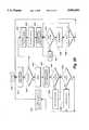
- FIG. 1is a system level block diagram of the popular Intel Pentium® CPU 20, operating on local bus 22 access to a distributed memory 24 comprising SRAM cache and DRAM main memory.
- the local buscomprises data line 26, address line 28 and control line 30.
- a PCI controller 32 and device 34are also shown linked to distributed cache and main memory 24 by a PCI bus 36.
- the PCI busoperates at a slower clock speed than the local bus 22.
- the PCI buscomprises a multiplexed address and data line 38 and a control line 40.
- Block Acomprises an arbitration and control unit 46, a main memory 48, a cache 50 devoted to the local bus 22 and a cache 52 devoted to the PCI bus 36.
- Block Bis similarly configured, comprising an arbitration and control unit 54, a main memory 56, a cache 58 devoted to the local bus and a cache 60 devoted to the PCI bus.
- Cache 50includes rows 62, 64; cache 52 includes rows 66, 68; cache 58 includes rows 70, 72; and cache 60 includes rows 74, 76. Therefore, the unit value for the bus axis is 2, the unit value for the memory block is 2, and the unit value for the cache row is 2.
- a partially distributed cache arbitration and control policyis implemented in this preferred embodiment.
- the more distributed the cache arbitration and controlthe faster the system throughput.
- a partially distributed arrangementhas been shown in order to conserve memory block real estate. Partial arbitration and control occurs at a system level in system control and arbitration unit 78 which is used to arbitrate priority between concurrent requests; to determine whether a request for an address mapped to either memory or input/output is in fact for memory; and to control which memory block is being addressed. Additionally, unit 78 can promote pipelining behavior in the memory blocks.
- the system control and arbitration unit 78is connected by address and command line 80 and control line 82 to memory block 42, and by address and command line 84 and control line 86 to memory block 44. This replication of address and control lines between the system control and arbitration unit 78 and the memory blocks allows for increased throughput by providing for concurrent memory access to different blocks by each bus.
- control and arbitration units 46 and 54associated respectively with Block A 42 and Block B 44.
- control cache read/write policyand arbitrate between memory access and memory refresh as required by the volatile DRAM of main memory units 48, 56.
- Unit 42consists generally of an arbitration and control section 46. Within arbitration and control section 46 of memory block A 42 there are five basic hardware modules.
- Module 100contains hardware for the uploading of address and command from the system arbitration and control unit 78 to the local bus 104, 106 and PCI bus 108, 110 address and command buffers. Module 100 also contains hardware for downloading of these buffers to main memory 48 when such access is required.
- Module 150contains the hardware for processing local bus read hits and misses, and module 200 contains the circuitry for handling PCI bus read-hits and misses.
- Hardware module 250contains the circuitry for handling a write hit or miss as requested by either the PCI or local bus.
- Hardware module 300contains the comparator circuitry necessary to classify reads or writes as a hit or a miss.
- Hardware module 350contains the main block memory, the distributed cache directories and data 52, 50 for the PCI bus 36 and the local bus 22, and the refresh circuitry connected with maintaining a volatile DRAM main memory.
- the last hardware module, module 400contains the input/output control and data latching required for memory block 42.
- this moduleconsists of demultiplexer 102, local bus address 104 and command 106 buffers, PCI bus address 108 and command 110 buffers, multiplexer 118 and multiplexer drivers 112 and 114.
- Demultiplexer 102is driven by control signals received from the system arbitration and control unit 78 over signal lines 82. Address and command is provided over signal lines 80. In response to a control signal on lines 82, an address and command available on lines 80 is directed by demultiplexer 102 to the appropriate buffers, either local 104, 106 or PCI 108, 110.
- address and command line 80will convey multiplexed address information in the form of serially transmitted upper (row) and lower (column) address bytes.
- Upper byteswill be loaded by demultiplexer 102 into the upper bytes of the appropriate buffers either 104 or 108 and lower bytes will be loaded by demultiplexer 102 into the lower bytes of the appropriate buffers either 104 or 108.
- loading of buffers 104 or 108will involve writing only to the lower bytes of the buffer leaving the upper bytes unchanged. This latter mode of addressing reduces the transmission time for JEDEC® standard address information involving consecutive address read/write requests directed to different columns (lower bytes) within the same row (upper byte) of memory.
- a burst write in this contextis a series of consecutive writes to the columns within the same row of memory.
- Multiplexer 118is involved in the downloading of the contents of local bus buffer 104, 106 or PCI bus buffers 108, 110 to main memory.
- the determination of which of these buffers to be downloaded to main memory, when these buffers are to be downloaded to main memory and if these buffers are to be downloaded to main memoryis made by skip and inhibit multiplexer control circuits 112 and 114.
- Skip circuit 112is responsible for determining which is the next buffer to be processed and for determining whether that buffer requires a memory download. If, for example, skip circuit 112 determines that the buffer eligible for downloading can be handled instead through cache as a read hit, then the downloading of that buffer will be skipped.
- inhibit circuitry 114determines when the appropriate time for that downloading is. If, for example, main memory is currently under a refresh or processing a prior download, then inhibit circuit 114 will prevent multiplexer signal 116 from enabling the multiplexer in choosing which buffer to download until such time as the inhibiting factors have been removed.
- Signals emanating from hardware module 100include signal 120 which contains the command available in command buffer 106. This command, either a read or write, would have been initially obtained by the system arbitration and control unit off the W/R line on the local bus.
- Signal 122contains the command, read/write, in the PCI bus command buffer 110. This signal was originally derived from the PCI bus C/BE# multiplexed control line as described in the ensuing discussion of PCI bus protocols.
- Signal line 124contains the address downloaded from system arbitration and control unit 78 and initially derived from the local bus A 31:3! address line.
- Signal line 126contains the address downloaded from the system arbitration and control unit from the PCI bus and initially available on the multiplexed AD lines of that bus.
- Signal lines 128 and 130contain respectively the address and command, read/write, downloaded to main memory by multiplexer 118 from either the local bus buffers 104, 106 or PCI bus buffers 108, 110.
- the next hardware module 150contains the circuitry connected with processing read hits and misses originating from the local bus.
- Transmission gate 152imposes a precondition on the processing of a local bus buffer 106 read.
- NAND gate driver 154accepting signal inputs 306 and 128 requires in order to enable the transmission gate 152 that there not be a write command being processed at the memory level which requires updating of stale data found in local bus cache 50. This condition would be present, for example, when local bus cache comparator line 306 was active and when memory level command line 130 was active indicating that a write was in process and local bus cache 50 contained stale data.
- transmission gate 152When the disabling conditions are not found, transmission gate 152 would be enabled.
- the enabled output of transmission gate 152is one input of AND gate 156.
- the other inputis from local bus comparator 302 via signal line 308.
- AND gate 156senses a read command from the local bus buffer and a hit on line 306, it is active. Under these conditions, a read hit would be in order and all data is read from local bus cache 50.
- the enabled output of AND gate 156would be presented to an input of OR gate 158 thereby driving burst interval countdown circuit 160, an output of which is burst enable signal 162.
- a burst readis defined to be the serial transfer of data packets (columns) from a row of cache.
- Circuit 166detects the presence of a local bus buffer read miss. If, for example, a read is present on enabled transmission gate 152 output and the AND gate 156 has not detected a read hit, then a read miss is being processed.
- Skip circuitry 112will identify local bus buffers 104, 106 as requiring a memory download. When the contents of local bus buffers 104, 106 have been copied to main memory, inhibit circuit 164 will sense that condition. This condition in conjunction with a read miss on lines 120 and 308 activates delay off circuit 166. When delay off circuit 166 is enabled, signals 172 and 170 are active. Signal 172 will enable transmission gate 360.
- Signal 170will activate main memory 48. Under these conditions the requested address and data will be uploaded from main memory 48 to cache 50. At an appropriate interval after activation of circuit 166, delay on circuit 168 will enable its output thereby transmitting an active signal to an input of OR gate 158 which will drive burst interval countdown circuitry thereby emitting a burst enable signal 162. After initial loading of cache 50 from main memory 48, all data is read in burst mode from cache 50.
- the next hardware module 200is almost identical to that of hardware module 150 except for those differences required by the difference in bus protocols on the PCI as opposed to the local bus.
- Transmission gate 202specifically imposes the precondition on PCI buffer read analysis that there not be a current memory write access which requires updating of the contents of PCI cache 52. If this limiting condition is indicated, then lines 130 and 308 serving respectively as the memory level command status and PCI cache comparator inputs to AND gate 204 will be active. Under these conditions NAND gate will be inactive thereby disabling transmission gate 202.
- Circuit 218detects the presence of a PCI bus buffer read miss. If, for example, a read is present on enabled transmission gate 202 output and the AND gate 206 has not detected a read hit, then a read miss is being processed.
- Skip circuitry 112will identify PCI bus buffers 108, 110 as requiring a memory download. When contents of the PCI bus buffers have been copied to main memory, inhibit circuit 216 will sense that condition. That condition in conjunction with a read miss on lines 122 and 308 activates delay off circuit 220. When delay off circuit 218 is enabled, signal 224 and 222 are active. Signal 224 will enable transmission gate 362.
- Signal 222will activate main memory 48. Under these conditions the requested address and data will be uploaded from main memory 48 to cache 52. At an appropriate interval after activation of circuit 218, delay on circuit 220 will enable its output thereby transmitting an active signal to an input of OR gate 208 which will enable an input of AND gate 210. As long as the FRAME# input to AND gate 210 is also active, a burst enable signal 214 will be present at the output of AND gate 214.
- the next hardware module 250is connected with processing memory access writes.
- a write signalis detected on line 130 by delay off circuitry 252
- an active signal 258is sent to the inputs of OR gate 352 thereby enabling access to main memory 48.
- an active signal 172will be sent to transmission gate 360 enabling the copying of new data from main memory 48 to replace the stale data in cache 50.
- an active signal 224will be passed to transmission gate 362 thereby enabling the copying of data written to main memory to cache 52 to refresh stale data in the PCI cache.
- hardware module 250handles the processing of write hits and misses.
- the next hardware module 300is generally concerned with handling local bus cache comparisons and PCI bus cache comparisons by means of comparators 302 and 304, respectively.
- Local bus cache comparator 302has two inputs: input 372 from an address portion of cache 50 and input 318 from either transmission gate 310 or transmission gate 314.
- PCI cache comparator 304has two inputs: specifically, signal 382 from an address portion of cache 52 and signal 320 from either transmission gate 312 or transmission gate 316.
- Transmission gates 310, 312operate in unison; transmission gates 314, 316 operate in unison and in opposition to transmission gates 310, 312. When one pair is enabled, such as 310, 312, the other is disabled. Transmission gate 310 inputs are coupled to local bus address buffers 104; signal lines 124 and transmission gate 312 inputs are coupled to the PCI address buffers 108 signal lines 126. Transmission gates 314 and 316 inputs are coupled to address lines 128.
- Transmission gates 310 and 312are driven active, in other words, enabled when control line 130 indicates a read. Alternately, when control line 130 indicates a write, transmission gates 310 and 312 are disabled and transmission gates 314 and 316 are enabled. This transmission gate circuitry is required in order to maintain cache coherency. During a write access to main memory 48, caches 50, 52 in memory block 42 are unified, and during a read access, caches 50, 52 are distributed. This ensures cache coherency amongst all caches in a given memory block during a write while still allowing for each cache to perform in a distributed manner when a read is being processed.
- the next hardware module 350contains main memory 48, local bus and PCI bus caches 50 and 52, respectively, and refresh circuitry 354.
- Local bus cache 50, data output 370is driven by burst column and latch circuitry 368.
- Circuit 368is programmed in the case of a Pentium® local bus for burst generation in the Intel® interleaved burst mode format.
- a burst enable signal 162is detected at the inputs of AND gate 364, and is coupled with CPU clock signal 366, the output of AND gate 364 enables the circuitry in burst column and latch circuit 368.
- the output of burst column and latch circuit 368causes specific data packets contained in cache 50 to be output.
- Cache 52the PCI cache for this particular memory block, provides linear burst mode data on signal lines 380.
- the operation of cache 52is determined by burst column and latch circuitry 384.
- This circuitryis preprogrammed to a linear burst mode appropriate for the PCI bus protocol.
- the burst column and latch circuitry 384is activated when AND gate 374 detects the presence of PCI clock signal 376, a burst enable PCI signal 214, and the absence of a wait state introduced by the PCI bus master in the form, for example, of an IRDY# signal. When these conditions are detected, burst column and latch circuitry 384 is enabled by the output of AND gate 374.
- the output of burst column and latch circuit 384causes specific data packets contained in cache 52 to be output in an PCI linear burst mode format on data lines 380.
- burst column and latch circuit 368 and 384would contain a start column address buffer and latch which is independently programmable over input lines 80 and 82. Under these circumstances the address portion of 50, 52 would contain the most significant bits of an address corresponding to a row in DRAM main memory 48.
- An access to main memory 48is enabled when any one of the inputs of OR gate 352 are active.
- access to main memoryis enabled when signal line 170 is active thereby indicating the processing of a local bus read miss, when signal line 222 is active indicating the processing of a PCI bus read miss, or when signal line 258 is active indicating the processing of a memory access write.
- signal line 170is active thereby indicating the processing of a local bus read miss
- signal line 222is active indicating the processing of a PCI bus read miss
- signal line 258is active indicating the processing of a memory access write.
- transmission gates 360 nor 362will be enabled when a write is being processed by main memory as indicated by a write on line 130.
- neither transmission gates 360 nor 362will be enabled in the event of a write hit.
- either one or both of transmission gates 360 or 362will be enabled depending on which caches contain stale data that needs to be updated in order to maintain coherency between caches 50, 52 and main memory 48. Both caches need to be updated only if both contain data for the same memory address as that being written to.
- Multiplexer 356provides access to main memory either for the refresh address provided by refresh circuitry 354 or for the memory access address available on lines 128.
- Multiplexer control signal 358is in traditional EDRAM parlance the /F signal. When signal line 358 is active, refresh address generation circuitry 354 is enabled and row by row refreshing of main memory 48 is accomplished. Alternately, when multiplexer control line 358 is not active, in other words, refresh is not in progress, then the address made available to main memory is that address present on memory access signal lines 128.
- Circuit 402is the input/output control and data latching connected with the local bus
- circuit 404is the input/output control and data latching connected with the PCI bus.
- Control lines 30provide the appropriate signals for local bus data management to circuit 402. For example, during a read cycle signal BRDY# would be available on a control line 30 to indicate the presence of data available to be read on bus 26. When no local bus memory access was directed to memory block 42, the circuit 402 would tristate its outputs to local bus 26.
- circuitry of unit 404is a little more complicated due to the wait states that can be introduced on the PCI bus and the multiplexed protocol for handling both address and data. Therefore, circuitry in 404 must, through control lines 40, handle transmission and receipt handshakes with signals, TRDY#, IRDY#, and demultiplexing an AD line with signals DEVSEL and FRAME#.
- circuitry of 402, 404 and in system arbitration and control unit 78 that is connected with bus protocol and data managementis set forth in the references.
- the basic hardware, however, for handling distributed cache and distributed arbitration and controlhave been set forth in FIGS. 1-2 and, although many hardware realizations of this distributive cache policy can be implemented, the central characteristics of distributed cache control from a hardware perspective have been set forth. What remains is to describe from a process point of view the method of the current invention.
- FIGS. 3A-DThese process flow diagrams reflect the basic considerations applicable to interfacing multiple buses with a tightly coupled and distributively cached memory.
- Each busis characterized as communicating with memory in terms of: clock, announcement, command, address, wait, data, and completion. Both buses in this preferred embodiment operate in burst mode.
- Maximum burst duration for the PCI busis assumed to have been initialized at the PCI bridge and burst mode interleaved/linear is assumed to have been set at the burst mode generator in each memory block.
- FIG. 3AThe processing within system level arbitration and control unit 78 is shown in FIG. 3A.
- start block 500two parallel paths process announcements, commands, and addresses occurring on the local bus and the PCI bus.
- next clock 502 determinationleads to decision step 504 in which the local Pentium® bus is probed for traffic. If ADS# and a valid address are present, then there is an announcement on the local bus 22 and control is passed to decision block 506. Alternately, if there is no announcement on the CPU bus, then control returns to process block 502 for a determination of the status of the local bus coinciding with the next clock cycle. When an announcement is detected in decision block 504, then control is passed to decision block 506 to determine if the bus traffic concerns a memory request or an I/O request as indicated by line M/IO#. If the announcement and request is not for memory, then control returns to process block 502.
- process block 508the address on line A 31:3! and the command, read/write, on line CPUW/R# are stored in a system level local bus address and command buffer in system arbitration and control unit 78.
- process 510the address and the command are sent over either line 80 or line 84 as shown in FIG. 1, depending on the memory block to which they are directed.
- the address and commandare stored in memory block-level local bus buffers in the appropriate memory block 42 or 44 as determined by control signals 82 or 86.
- process 512the address that was stored in the system level local bus address buffer in step 508 is cleared. Then control returns to process 502 for a determination of the next clock.
- the PCI bus processingbegins at the next clock 514 determination. This leads to the determination in step 116 of bus traffic on the PCI bus 36. If FRAME# is asserted and a valid address AD are present, then there is an announcement and control is passed to decision block 518. Alternately, if there is no announcement on the PCI bus, then control returns to process block 514 for a determination of the status of the bus coinciding with the next clock cycle. When an announcement is detected by decision block 516, then control is passed to decision block 518 to determine if the PCI bus traffic concerns a memory request or an I/O request. If the announcement and request is not for memory, then control returns to process block 514. If, alternately, there is a request for a valid memory address, then in process block 520 the address on line AD and the command, read or write, on line C/BE# is stored in an address and command buffer respectively.
- arbitrationmay be needed if a concurrent request directed to the same memory block is being processed on the CPU path 502, 504, 506, 508. If concurrent requests are for addresses contained in separate memory blocks, then they can be processed in parallel by control lines 82, 86 servicing, respectively, memory blocks 42 and 44 as shown in FIG. 1. If, alternately, concurrent PCI and local bus requests are directed to addresses mapped to one memory block, then priority will need to be established. In the preferred embodiment, priority control is passed from process 520 to process 522 for a comparison of the addresses stored in process steps 508 and 520. Then in decision process 524, a determination is made as to whether the address announced by the local bus 22 and the PCI bus 36 are mapped to the same memory block.
- a wait stateis introduced in the processing of the PCI traffic, thereby giving priority to local bus traffic. It is desirable to give priority to the local bus because it is the faster bus and because its memory accesses are of a defined and shorter duration than those of the PCI bus.
- the wait state controlpasses to process 528. If, alternately, the result of decision 524 is that the addresses being concurrently processed are not mapped to the same memory block, then in process 528 the address and the command stored in step 520 are sent over either line 80 or line 84 as shown in FIG. 1, depending on the memory block to which they are directed. The address and command are stored in memory block-level PCI buffers in the appropriate memory block 42 or 44.
- process 530the address that was stored in the system level PCI address buffer in step 520 is cleared. Then control returns to process 514 for a determination of the next clock.
- arbitration of priority between concurrent requests, of mapping a request to memory or I/O, and of mapping a memory request to a specific memory blockis being handled at a system level. It would be equally possible to handle these tasks at a memory block-level. This would increase system throughput and would require that most of the circuitry connected with implementing the processes of FIG. 3A be duplicated in each memory block. Either approach may be suitable.
- FIG. 3Bis a process flow diagram of memory block-level processing of memory requests and main memory accesses occurring, possibly concurrently, in each memory block.
- the block-level local and PCI buffershave been loaded in steps 510 and 528, respectively. It remains to process those buffers.
- controlis passed to process block 552.
- process 552the determination of the next block-level buffer to be processed, and perhaps passed to block-level main memory, is commenced.
- Controlis passed to decision 554 in which the next buffers, in this case either block-level local bus or PCI bus, are analyzed. If null, then the current buffers have not been downloaded with an address or command and control returns to process 552 for polling of the next buffers.
- decision 558a determination is made as to whether the portion of main memory associated with this memory block is currently under an inhibit status which could, for example, be due either to a refresh of this block's main DRAM memory as indicated by the signal /F 358 and /RE 170, 258, 222 being active, or by a main memory access of this block as indicated by signal /RE being active. /RE will be active when either a block-level read miss or write is being handled. If either of these inhibits are taking place, then control passes to process 560 for the introduction of a wait state after which control returns to decision 558.
- process 562in which the block-level buffers, in this case either local or PCI, are presented to block-level main memory for processing. Subsequently, control passes to process 552.
- FIG. 3Ba cycle of memory block-level buffer analysis and block-level main memory downloading has been detailed.
- FIG. 3Cthe processing of a read hit at a memory block-level for the local bus buffers is detailed.
- the processes shownapply generally to each of the memory block-level bus buffers. In other words, the process shown in FIG. 3C occurs with respect to both the local and PCI bus memory block-level buffers.
- controlpasses to process block 582 in which the loading of a new set of address and control requests into the local bus buffers is detected.
- Controlis then passed to decision block 586 in which it is determined whether at the block main memory level a write condition is present, and further, at the local bus buffer level whether a hit condition has been detected, in which event control passes to process block 588 for the introduction of a wait state. This allows time for the current memory access to refresh stale cache data in the local bus cache within this memory block.
- controlreturns to decision block 584 and proceeds in that 584, 586 loop until such time as the current memory access no longer involves a write condition coupled with a local bus cache write hit.
- decision block 588a determination is made as to whether a read is requested by the memory block-level local bus buffers, and further whether the address to which the read is directed is currently contained in memory block-level local bus cache. In the event that a read hit is not detected, then no read cycle independent of main memory access can take place and control returns to process block 582.
- the burst modeis activated for the memory block-level local bus cache. If the signal protocol on the local bus calls for a burst notification, that command is sent at this point. If this process loop were directed to the PCI bus, rather than the local bus, this burst notification would be evidenced by the TRDY# line being activated.
- process block 592to which control has passed, a burst countdown is activated, which in this case is necessary, because Pentium® local bus burst cycles are of a predetermined length.
- This processcould be eliminated in the event of a PCI bus, in which case burst length is not fixed.
- decision block 594in which case a determination is made as to whether a wait state is required. There are no wait states on the local bus, but if this process were for the PCI bus, for example, a determination would be made as to whether IRDY# were asserted.
- controlwould pass to process block 596 for the introduction of a wait state and return to decision block 594 for determination of when a wait state was no longer present.
- decision block 594Once the determination in decision block 594 is in the negative, in other words, that no wait state exists, then control passes to process block 596 in which the next data packet is transmitted from the memory block-level local bus cache.
- decision block 600subsequently passes to decision block 600 for determination as to whether or not the burst interval has ended. In the case of a Pentium® bus, this would involve determining whether the burst countdown had reached a null state in which case the burst interval just engaged in was the last interval.
- controlis passed to process block 622 in which the passage 662 of the next buffers from the control and arbitration unit of a given memory block to the main memory of that block is indicated.
- decision 624for determination of whether that specific memory access is a read miss access. The determination of a read miss is made by comparing only the cache directory dedicated to the bus from which the read request was received and the requested address. The other caches of the memory block devoted to other buses are not involved in this determination.
- controlis passed to process 626 in which the appropriate cache servicing the specific bus from which the read request was received is enabled, and a copy of the data to be read is uploaded to the block-level cache for that bus from the main memory of that block.
- Controlis subsequently passed to process block 628 in which, after the upload to the appropriate cache has taken place, main memory access is terminated.
- process block 630in which burst mode is activated; a burst notification, as mentioned previously and if required by the bus protocol is sent; and a burst countdown in the case of a Pentium® bus read request is activated.
- controlis passed to decision 632 for determination as to whether a wait state has been introduced into the cache access. If, for example, the read access is from the PCI bus, then the assertion of IRDY# would indicate a wait state was required until the master was ready to receive the data available within the memory block-level PCI cache. If decision 632 is in the affirmative, then control is passed to process block 634 for the introduction of a wait state and subsequent return to decision block 632. Once the removal of a wait state or absence of a wait state is detected, control is passed to process block 636 for transmission of the next data burst.
- controlis passed to decision block 638 in which it is determined whether the burst interval is over. In the case of the local bus, this would be indicated by the null state of the burst countdown; in the case of the PCI bus this would be indicated by the deactivation of FRAME#. In the event the determination is in the negative, for example, that the burst cycle is not completed, then control returns to decision block 632. Alternately, if it is determined that the burst interval has terminated, then control is passed to process block 622 for retrieval of the next buffers requiring access to block-level main memory.
- the block-level main memory access taking placeis a write cycle 640.
- Controlthen is passed to process 642 in which all cache comparators in a specific memory block are linked and perform as a unified rather than distributed cache.
- the comparison being made by these comparatorsis between all cache directories in the memory block, in this case a local bus and PCI bus cache, and the address present in main memory. This is required to assure that all stale data irrespective of the cache in which it is found is updated during this write hit.
- controlis passed to decision block 644 for determination of whether a local bus write cache hit is detected.
- controlis passed to process block 646, in which case the transmission gate to the local bus cache is enabled and a copy of the new data just written to main memory is also copied from main memory to the appropriate row in the local bus cache.
- Controlis then returned to decision block 648.
- decision block 648Alternately, if there is not a local bus cache write hit as determined in decision block 644, then control is also passed to decision block 648. This is required because on a memory write both the local and PCI caches may contain identical addresses requiring updating of stale data.
- decision block 648determination is made as to whether a hit has been experienced in the memory block-level PCI cache. In the event that it has, control is passed to process block 650 for subsequent uploading of a copy of the data just written to main memory to the PCI cache. Control is then passed to process block 652. Alternately, if a determination 648 is made that there is no PCI cache write hit, then control is passed also to process block 652 for terminating main memory access and for uncoupling the comparators of the memory block and returning them to their normal separated state. In this state each comparator compares a memory block-level cache directory with the address present in the memory block-level address buffer associated with that bus.
- the current distributive cache and cache arbitration and controlexhibits the following advantages.
- any memory requests on the local and PCI bus, including dual write hitscan be processed concurrently in the current system, provided that the hits occur in different memory blocks.
- Any memory requests in an L2 cacheare handled serially.
- Second, of those memory requests on the local and PCI buses which are directed to a single memory blockthe following can be performed concurrently in the current system: dual read hits, a read miss and a read hit, a-read hit and a write miss, and a read hit and a write hit; provided in the latter case the hit is not in the cache involved in the read hit.
- an L2 cacheall memory requests are handled serially.
- a bus transactionconsists of an address phase followed by one or more data phases. PCI supports both read and write bursts.
- the address phaseis the clock cycle in which FRAME# is asserted.
- AD 31:0!contain a physical address (32 bits). For I/O, this is a byte address; for configuration and memory, it is a DWORD address.
- AD 07:0!contain the least significant byte (lsb) and AD 31:24! contain the most significant byte (msb).
- Write datais stable and valid when IRDY# is asserted and read data is stable and valid when TRDY# is asserted. Data is transferred during those clocks where both IRDY# and TRDY# are asserted.
- C/BE 3:0!# Bus Command and Byte Enablesare multiplexed on the same PCI pins.
- C/BE 3:0!#define the bus command (refer to Section 3.1. for bus command definitions).
- C/BE 3:0!#are used as Byte Enables.
- the Byte Enablesare valid for the entire data phase and determine which byte lanes carry meaningful data.
- C/BE O!#applies to byte 0 (lsb) and C/BE 3!# applies to byte 3 (msb).
- FRAME# Cycle Frameis driven by the current master to indicate the beginning and duration of an access. FRAME# is asserted to indicate a bus transaction is beginning. While FRAME# is asserted, data transfers continue. When FRAME# is deasserted, the transaction is in the final data phase.
- IRDY# Initiator Readyindicates the initiating agent's (bus master's) ability to complete the current data phase of the transaction. IRDY# is used in conjunction with TRDY#. A data phase is completed on any clock both IRDY# and TRDY# are sampled asserted. During a write, IRDY# indicates that valid data is present on AD 31:0!. During a read, it indicates the master is prepared to accept data. Wait cycles are inserted until both IRDY# and TRDY# are asserted together.
- TRDY# Target Readyindicates the target agent's (selected device's) ability to complete the current data phase of the transaction.
- TRDY#is used in conjunction with IRDY#. A data phase is completed on any clock both TRDY# and IRDY# are sampled asserted.
- TRDY#indicates that valid data is present on AD 31::00!.
- TRDY#indicates the target is prepared to accept data. Wait cycles are inserted until both IRDY# and TRDY# are asserted together.
- STOP# Stopindicates the current target is requesting the master to stop the current transaction.
- DEVSEL# Device Select when actively drivenindicates the driving device has decoded its address as the target of the current access. As an input, it indicates whether any device on the bus has been selected.
- BRDY# Burst Readyallows the CPU to insert wait states as necessary to meet the memory subsystems timing requirements.
- ADS# Address Strobeindicates the availability of a valid address on the local bus.
- NA Next Addressallows for pipelining address and data commands by signaling the processor that, although the data portion of the previous command is still being processed, the address portion is complete and a new address for the next operation can be made available on the bus.
Landscapes
- Engineering & Computer Science (AREA)
- Theoretical Computer Science (AREA)
- General Engineering & Computer Science (AREA)
- Physics & Mathematics (AREA)
- General Physics & Mathematics (AREA)
- Computer Hardware Design (AREA)
- Memory System Of A Hierarchy Structure (AREA)
Abstract
Description
Claims (34)
Priority Applications (3)
| Application Number | Priority Date | Filing Date | Title |
|---|---|---|---|
| US08/521,597US5802560A (en) | 1995-08-30 | 1995-08-30 | Multibus cached memory system |
| EP96304565AEP0762287A1 (en) | 1995-08-30 | 1996-06-19 | Multibus cached memory system |
| JP8230420AJPH09138764A (en) | 1995-08-30 | 1996-08-30 | Multibus cache-type memory system |
Applications Claiming Priority (1)
| Application Number | Priority Date | Filing Date | Title |
|---|---|---|---|
| US08/521,597US5802560A (en) | 1995-08-30 | 1995-08-30 | Multibus cached memory system |
Publications (1)
| Publication Number | Publication Date |
|---|---|
| US5802560Atrue US5802560A (en) | 1998-09-01 |
Family
ID=24077353
Family Applications (1)
| Application Number | Title | Priority Date | Filing Date |
|---|---|---|---|
| US08/521,597Expired - Fee RelatedUS5802560A (en) | 1995-08-30 | 1995-08-30 | Multibus cached memory system |
Country Status (3)
| Country | Link |
|---|---|
| US (1) | US5802560A (en) |
| EP (1) | EP0762287A1 (en) |
| JP (1) | JPH09138764A (en) |
Cited By (53)
| Publication number | Priority date | Publication date | Assignee | Title |
|---|---|---|---|---|
| US20020059491A1 (en)* | 1997-07-25 | 2002-05-16 | Atsushi Date | Bus management based on bus status |
| US6493776B1 (en) | 1999-08-12 | 2002-12-10 | Mips Technologies, Inc. | Scalable on-chip system bus |
| US20030041215A1 (en)* | 2001-08-27 | 2003-02-27 | George Robert T. | Method and apparatus for the utilization of distributed caches |
| US20030048677A1 (en)* | 2001-09-11 | 2003-03-13 | Seiko Epson Corporation | Semiconductor device having a dual bus, dual bus system, shared memory dual bus system, and electronic instrument using the same |
| US6604159B1 (en) | 1999-08-12 | 2003-08-05 | Mips Technologies, Inc. | Data release to reduce latency in on-chip system bus |
| US20030204684A1 (en)* | 2002-04-25 | 2003-10-30 | Schulz Jurgen M. | Distributed caching mechanism for pending memory operations within a memory controller |
| US6681283B1 (en)* | 1999-08-12 | 2004-01-20 | Mips Technologies, Inc. | Coherent data apparatus for an on-chip split transaction system bus |
| US20050044259A1 (en)* | 2001-06-04 | 2005-02-24 | Wilson James C. | Resolving crossing requests in multi-node configurations |
| US6977656B1 (en) | 2003-07-28 | 2005-12-20 | Neomagic Corp. | Two-layer display-refresh and video-overlay arbitration of both DRAM and SRAM memories |
| CN100472494C (en)* | 2007-02-05 | 2009-03-25 | 北京中星微电子有限公司 | System and method for implementing memory mediation of supporting multi-bus multi-type memory device |
| US20110198804A1 (en)* | 2002-02-08 | 2011-08-18 | Lynn Hessing | Image capturing card shuffler |
| US9220971B2 (en) | 2006-05-31 | 2015-12-29 | Bally Gaming, Inc. | Automatic system and methods for accurate card handling |
| US9220972B2 (en) | 2001-09-28 | 2015-12-29 | Bally Gaming, Inc. | Multiple mode card shuffler and card reading device |
| US9233298B2 (en) | 2009-04-07 | 2016-01-12 | Bally Gaming, Inc. | Playing card shuffler |
| US9259640B2 (en) | 2007-06-06 | 2016-02-16 | Bally Gaming, Inc. | Apparatus, system, method, and computer-readable medium for casino card handling with multiple hand recall feature |
| US9266012B2 (en) | 1998-04-15 | 2016-02-23 | Bally Gaming, Inc. | Methods of randomizing cards |
| US9266011B2 (en) | 1997-03-13 | 2016-02-23 | Bally Gaming, Inc. | Card-handling devices and methods of using such devices |
| US9320964B2 (en) | 2006-11-10 | 2016-04-26 | Bally Gaming, Inc. | System for billing usage of a card handling device |
| US9345952B2 (en) | 2006-03-24 | 2016-05-24 | Shuffle Master Gmbh & Co Kg | Card handling apparatus |
| US9345951B2 (en) | 2001-09-28 | 2016-05-24 | Bally Gaming, Inc. | Methods and apparatuses for an automatic card handling device and communication networks including same |
| US9370710B2 (en) | 1998-04-15 | 2016-06-21 | Bally Gaming, Inc. | Methods for shuffling cards and rack assemblies for use in automatic card shufflers |
| US9378766B2 (en) | 2012-09-28 | 2016-06-28 | Bally Gaming, Inc. | Card recognition system, card handling device, and method for tuning a card handling device |
| US9387390B2 (en) | 2005-06-13 | 2016-07-12 | Bally Gaming, Inc. | Card shuffling apparatus and card handling device |
| USD764599S1 (en) | 2014-08-01 | 2016-08-23 | Bally Gaming, Inc. | Card shuffler device |
| US9452346B2 (en) | 2001-09-28 | 2016-09-27 | Bally Gaming, Inc. | Method and apparatus for using upstream communication in a card shuffler |
| US9474957B2 (en) | 2014-05-15 | 2016-10-25 | Bally Gaming, Inc. | Playing card handling devices, systems, and methods for verifying sets of cards |
| US9504905B2 (en) | 2014-09-19 | 2016-11-29 | Bally Gaming, Inc. | Card shuffling device and calibration method |
| US9511274B2 (en) | 2012-09-28 | 2016-12-06 | Bally Gaming Inc. | Methods for automatically generating a card deck library and master images for a deck of cards, and a related card processing apparatus |
| US9539494B2 (en) | 2009-04-07 | 2017-01-10 | Bally Gaming, Inc. | Card shuffling apparatuses and related methods |
| US9566501B2 (en) | 2014-08-01 | 2017-02-14 | Bally Gaming, Inc. | Hand-forming card shuffling apparatuses including multi-card storage compartments, and related methods |
| US9616324B2 (en) | 2004-09-14 | 2017-04-11 | Bally Gaming, Inc. | Shuffling devices including one or more sensors for detecting operational parameters and related methods |
| US9623317B2 (en) | 2006-07-05 | 2017-04-18 | Bally Gaming, Inc. | Method of readying a card shuffler |
| US9713761B2 (en) | 2011-07-29 | 2017-07-25 | Bally Gaming, Inc. | Method for shuffling and dealing cards |
| US9731190B2 (en) | 2011-07-29 | 2017-08-15 | Bally Gaming, Inc. | Method and apparatus for shuffling and handling cards |
| US9764221B2 (en) | 2006-05-31 | 2017-09-19 | Bally Gaming, Inc. | Card-feeding device for a card-handling device including a pivotable arm |
| US9802114B2 (en) | 2010-10-14 | 2017-10-31 | Shuffle Master Gmbh & Co Kg | Card handling systems, devices for use in card handling systems and related methods |
| US9849368B2 (en) | 2012-07-27 | 2017-12-26 | Bally Gaming, Inc. | Batch card shuffling apparatuses including multi card storage compartments |
| US9993719B2 (en) | 2015-12-04 | 2018-06-12 | Shuffle Master Gmbh & Co Kg | Card handling devices and related assemblies and components |
| US10022617B2 (en) | 2001-09-28 | 2018-07-17 | Bally Gaming, Inc. | Shuffler and method of shuffling cards |
| US10279245B2 (en) | 2014-04-11 | 2019-05-07 | Bally Gaming, Inc. | Method and apparatus for handling cards |
| US10339765B2 (en) | 2016-09-26 | 2019-07-02 | Shuffle Master Gmbh & Co Kg | Devices, systems, and related methods for real-time monitoring and display of related data for casino gaming devices |
| US10394719B2 (en) | 2017-01-25 | 2019-08-27 | Samsung Electronics Co., Ltd. | Refresh aware replacement policy for volatile memory cache |
| US10456659B2 (en) | 2000-04-12 | 2019-10-29 | Shuffle Master Gmbh & Co Kg | Card handling devices and systems |
| US10532272B2 (en) | 2001-09-28 | 2020-01-14 | Bally Gaming, Inc. | Flush mounted card shuffler that elevates cards |
| US20200050557A1 (en)* | 2018-08-10 | 2020-02-13 | Beijing Baidu Netcom Science And Technology Co., Ltd. | Apparatus for Data Processing, Artificial Intelligence Chip and Electronic Device |
| US10785014B2 (en)* | 2017-02-07 | 2020-09-22 | Omron Corporation | Computation device, control device and control method |
| US10933300B2 (en) | 2016-09-26 | 2021-03-02 | Shuffle Master Gmbh & Co Kg | Card handling devices and related assemblies and components |
| US11173383B2 (en) | 2019-10-07 | 2021-11-16 | Sg Gaming, Inc. | Card-handling devices and related methods, assemblies, and components |
| US11338194B2 (en) | 2018-09-28 | 2022-05-24 | Sg Gaming, Inc. | Automatic card shufflers and related methods of automatic jam recovery |
| US11376489B2 (en) | 2018-09-14 | 2022-07-05 | Sg Gaming, Inc. | Card-handling devices and related methods, assemblies, and components |
| US11898837B2 (en) | 2019-09-10 | 2024-02-13 | Shuffle Master Gmbh & Co Kg | Card-handling devices with defect detection and related methods |
| US11896891B2 (en) | 2018-09-14 | 2024-02-13 | Sg Gaming, Inc. | Card-handling devices and related methods, assemblies, and components |
| US12290745B2 (en) | 2018-09-14 | 2025-05-06 | Sg Gaming, Inc. | Card-handling devices and related methods, assemblies, and components |
Families Citing this family (2)
| Publication number | Priority date | Publication date | Assignee | Title |
|---|---|---|---|---|
| KR100381615B1 (en)* | 2001-01-04 | 2003-04-26 | (주)실리콘세븐 | SRAM Compatible Memory For Complete Hiding of The Refresh Operation Using a DRAM Cache Memory |
| FR2921507B1 (en)* | 2007-09-26 | 2011-04-15 | Arteris | ELECTRONIC MEMORY DEVICE |
Citations (11)
| Publication number | Priority date | Publication date | Assignee | Title |
|---|---|---|---|---|
| EP0489583A2 (en)* | 1990-12-05 | 1992-06-10 | NCR International, Inc. | Multiple processor cache control system |
| US5249282A (en)* | 1990-11-21 | 1993-09-28 | Benchmarq Microelectronics, Inc. | Integrated cache memory system with primary and secondary cache memories |
| US5257367A (en)* | 1987-06-02 | 1993-10-26 | Cab-Tek, Inc. | Data storage system with asynchronous host operating system communication link |
| US5293603A (en)* | 1991-06-04 | 1994-03-08 | Intel Corporation | Cache subsystem for microprocessor based computer system with synchronous and asynchronous data path |
| EP0588369A1 (en)* | 1992-09-18 | 1994-03-23 | Hitachi, Ltd. | A processor with cache memory used in receiving data from other processors |
| US5355467A (en)* | 1991-06-04 | 1994-10-11 | Intel Corporation | Second level cache controller unit and system |
| US5361391A (en)* | 1992-06-22 | 1994-11-01 | Sun Microsystems, Inc. | Intelligent cache memory and prefetch method based on CPU data fetching characteristics |
| EP0627688A1 (en)* | 1993-05-28 | 1994-12-07 | International Business Machines Corporation | Provision of accurate and complete communication between different bus architectures |
| US5408636A (en)* | 1991-06-24 | 1995-04-18 | Compaq Computer Corp. | System for flushing first and second caches upon detection of a write operation to write protected areas |
| WO1996011430A2 (en)* | 1994-10-03 | 1996-04-18 | International Business Machines Corporation | Coherency and synchronization mechanism for i/o channel controllers in a data processing system |
| US5517626A (en)* | 1990-05-07 | 1996-05-14 | S3, Incorporated | Open high speed bus for microcomputer system |
- 1995
- 1995-08-30USUS08/521,597patent/US5802560A/ennot_activeExpired - Fee Related
- 1996
- 1996-06-19EPEP96304565Apatent/EP0762287A1/ennot_activeWithdrawn
- 1996-08-30JPJP8230420Apatent/JPH09138764A/enactivePending
Patent Citations (11)
| Publication number | Priority date | Publication date | Assignee | Title |
|---|---|---|---|---|
| US5257367A (en)* | 1987-06-02 | 1993-10-26 | Cab-Tek, Inc. | Data storage system with asynchronous host operating system communication link |
| US5517626A (en)* | 1990-05-07 | 1996-05-14 | S3, Incorporated | Open high speed bus for microcomputer system |
| US5249282A (en)* | 1990-11-21 | 1993-09-28 | Benchmarq Microelectronics, Inc. | Integrated cache memory system with primary and secondary cache memories |
| EP0489583A2 (en)* | 1990-12-05 | 1992-06-10 | NCR International, Inc. | Multiple processor cache control system |
| US5293603A (en)* | 1991-06-04 | 1994-03-08 | Intel Corporation | Cache subsystem for microprocessor based computer system with synchronous and asynchronous data path |
| US5355467A (en)* | 1991-06-04 | 1994-10-11 | Intel Corporation | Second level cache controller unit and system |
| US5408636A (en)* | 1991-06-24 | 1995-04-18 | Compaq Computer Corp. | System for flushing first and second caches upon detection of a write operation to write protected areas |
| US5361391A (en)* | 1992-06-22 | 1994-11-01 | Sun Microsystems, Inc. | Intelligent cache memory and prefetch method based on CPU data fetching characteristics |
| EP0588369A1 (en)* | 1992-09-18 | 1994-03-23 | Hitachi, Ltd. | A processor with cache memory used in receiving data from other processors |
| EP0627688A1 (en)* | 1993-05-28 | 1994-12-07 | International Business Machines Corporation | Provision of accurate and complete communication between different bus architectures |
| WO1996011430A2 (en)* | 1994-10-03 | 1996-04-18 | International Business Machines Corporation | Coherency and synchronization mechanism for i/o channel controllers in a data processing system |
Non-Patent Citations (7)
| Title |
|---|
| "High Speed Bus Arbiter for Bus-Oriented Multiprocessor Systems," IBM Technical Disclosure Bulletin, vol. 28, No. 2, Jul. 1985, pp. 567-579. |
| "PCT Local Bus Specification Revision 2.0," PCI Special Interest Group, Hillsboro, OR (1993), pp. 9-18, 28-40. |
| High Speed Bus Arbiter for Bus Oriented Multiprocessor Systems, IBM Technical Disclosure Bulletin, vol. 28, No. 2, Jul. 1985, pp. 567 579.* |
| Kendall, Guy W., "Hands on Under the Hood--Inside the PCT Local Bus," BYTE, Feb. 1994, pp. 177-180. |
| Kendall, Guy W., Hands on Under the Hood Inside the PCT Local Bus, BYTE, Feb. 1994, pp. 177 180.* |
| PCT Local Bus Specification Revision 2.0, PCI Special Interest Group, Hillsboro, OR (1993), pp. 9 18, 28 40.* |
| Ramtron Specialty Memory Products Catalog, Oct. 1994, Colorado Springs, Colorado.* |
Cited By (115)
| Publication number | Priority date | Publication date | Assignee | Title |
|---|---|---|---|---|
| US9266011B2 (en) | 1997-03-13 | 2016-02-23 | Bally Gaming, Inc. | Card-handling devices and methods of using such devices |
| US6499076B2 (en)* | 1997-07-25 | 2002-12-24 | Canon Kabushiki Kaisha | Memory management for use with burst mode |
| US20020059491A1 (en)* | 1997-07-25 | 2002-05-16 | Atsushi Date | Bus management based on bus status |
| US7062664B2 (en) | 1997-07-25 | 2006-06-13 | Canon Kabushiki Kaisha | Bus management based on bus status |
| US9266012B2 (en) | 1998-04-15 | 2016-02-23 | Bally Gaming, Inc. | Methods of randomizing cards |
| US9561426B2 (en) | 1998-04-15 | 2017-02-07 | Bally Gaming, Inc. | Card-handling devices |
| US9370710B2 (en) | 1998-04-15 | 2016-06-21 | Bally Gaming, Inc. | Methods for shuffling cards and rack assemblies for use in automatic card shufflers |
| US9861881B2 (en) | 1998-04-15 | 2018-01-09 | Bally Gaming, Inc. | Card handling apparatuses and methods for handling cards |
| US6493776B1 (en) | 1999-08-12 | 2002-12-10 | Mips Technologies, Inc. | Scalable on-chip system bus |
| US6604159B1 (en) | 1999-08-12 | 2003-08-05 | Mips Technologies, Inc. | Data release to reduce latency in on-chip system bus |
| US6681283B1 (en)* | 1999-08-12 | 2004-01-20 | Mips Technologies, Inc. | Coherent data apparatus for an on-chip split transaction system bus |
| US10456659B2 (en) | 2000-04-12 | 2019-10-29 | Shuffle Master Gmbh & Co Kg | Card handling devices and systems |
| US7406582B2 (en)* | 2001-06-04 | 2008-07-29 | Fujitsu Limited | Resolving crossing requests in multi-node configurations |
| US20050044259A1 (en)* | 2001-06-04 | 2005-02-24 | Wilson James C. | Resolving crossing requests in multi-node configurations |
| US20030041215A1 (en)* | 2001-08-27 | 2003-02-27 | George Robert T. | Method and apparatus for the utilization of distributed caches |
| US20030048677A1 (en)* | 2001-09-11 | 2003-03-13 | Seiko Epson Corporation | Semiconductor device having a dual bus, dual bus system, shared memory dual bus system, and electronic instrument using the same |
| US9220972B2 (en) | 2001-09-28 | 2015-12-29 | Bally Gaming, Inc. | Multiple mode card shuffler and card reading device |
| US10022617B2 (en) | 2001-09-28 | 2018-07-17 | Bally Gaming, Inc. | Shuffler and method of shuffling cards |
| US10004976B2 (en) | 2001-09-28 | 2018-06-26 | Bally Gaming, Inc. | Card handling devices and related methods |
| US10532272B2 (en) | 2001-09-28 | 2020-01-14 | Bally Gaming, Inc. | Flush mounted card shuffler that elevates cards |
| US10549177B2 (en) | 2001-09-28 | 2020-02-04 | Bally Gaming, Inc. | Card handling devices comprising angled support surfaces |
| US9452346B2 (en) | 2001-09-28 | 2016-09-27 | Bally Gaming, Inc. | Method and apparatus for using upstream communication in a card shuffler |
| US10086260B2 (en) | 2001-09-28 | 2018-10-02 | Bally Gaming, Inc. | Method and apparatus for using upstream communication in a card shuffler |
| US10343054B2 (en) | 2001-09-28 | 2019-07-09 | Bally Gaming, Inc. | Systems including automatic card handling apparatuses and related methods |
| US10569159B2 (en) | 2001-09-28 | 2020-02-25 | Bally Gaming, Inc. | Card shufflers and gaming tables having shufflers |
| US10226687B2 (en) | 2001-09-28 | 2019-03-12 | Bally Gaming, Inc. | Method and apparatus for using upstream communication in a card shuffler |
| US9345951B2 (en) | 2001-09-28 | 2016-05-24 | Bally Gaming, Inc. | Methods and apparatuses for an automatic card handling device and communication networks including same |
| US9333415B2 (en) | 2002-02-08 | 2016-05-10 | Bally Gaming, Inc. | Methods for handling playing cards with a card handling device |
| US10092821B2 (en) | 2002-02-08 | 2018-10-09 | Bally Technology, Inc. | Card-handling device and method of operation |
| US20110198804A1 (en)* | 2002-02-08 | 2011-08-18 | Lynn Hessing | Image capturing card shuffler |
| US8720891B2 (en)* | 2002-02-08 | 2014-05-13 | Shfl Entertainment, Inc. | Image capturing card shuffler |
| US9700785B2 (en) | 2002-02-08 | 2017-07-11 | Bally Gaming, Inc. | Card-handling device and method of operation |
| US6959361B2 (en)* | 2002-04-25 | 2005-10-25 | Sun Microsystems, Inc. | Distributed caching mechanism for pending memory operations within a memory controller |
| US20030204684A1 (en)* | 2002-04-25 | 2003-10-30 | Schulz Jurgen M. | Distributed caching mechanism for pending memory operations within a memory controller |
| US6977656B1 (en) | 2003-07-28 | 2005-12-20 | Neomagic Corp. | Two-layer display-refresh and video-overlay arbitration of both DRAM and SRAM memories |
| USRE43565E1 (en) | 2003-07-28 | 2012-08-07 | Intellectual Ventures I Llc | Two-layer display-refresh and video-overlay arbitration of both DRAM and SRAM memories |
| US9616324B2 (en) | 2004-09-14 | 2017-04-11 | Bally Gaming, Inc. | Shuffling devices including one or more sensors for detecting operational parameters and related methods |
| US9387390B2 (en) | 2005-06-13 | 2016-07-12 | Bally Gaming, Inc. | Card shuffling apparatus and card handling device |
| US9908034B2 (en) | 2005-06-13 | 2018-03-06 | Bally Gaming, Inc. | Card shuffling apparatus and card handling device |
| US10576363B2 (en) | 2005-06-13 | 2020-03-03 | Bally Gaming, Inc. | Card shuffling apparatus and card handling device |
| US9345952B2 (en) | 2006-03-24 | 2016-05-24 | Shuffle Master Gmbh & Co Kg | Card handling apparatus |
| US10220297B2 (en) | 2006-03-24 | 2019-03-05 | Shuffle Master Gmbh & Co Kg | Card handling apparatus and associated methods |
| US9789385B2 (en) | 2006-03-24 | 2017-10-17 | Shuffle Master Gmbh & Co Kg | Card handling apparatus |
| US10926164B2 (en) | 2006-05-31 | 2021-02-23 | Sg Gaming, Inc. | Playing card handling devices and related methods |
| US9901810B2 (en) | 2006-05-31 | 2018-02-27 | Bally Gaming, Inc. | Playing card shuffling devices and related methods |
| US9220971B2 (en) | 2006-05-31 | 2015-12-29 | Bally Gaming, Inc. | Automatic system and methods for accurate card handling |
| US10525329B2 (en) | 2006-05-31 | 2020-01-07 | Bally Gaming, Inc. | Methods of feeding cards |
| US9764221B2 (en) | 2006-05-31 | 2017-09-19 | Bally Gaming, Inc. | Card-feeding device for a card-handling device including a pivotable arm |
| US10226686B2 (en) | 2006-07-05 | 2019-03-12 | Bally Gaming, Inc. | Automatic card shuffler with pivotal card weight and divider gate |
| US10639542B2 (en) | 2006-07-05 | 2020-05-05 | Sg Gaming, Inc. | Ergonomic card-shuffling devices |
| US9623317B2 (en) | 2006-07-05 | 2017-04-18 | Bally Gaming, Inc. | Method of readying a card shuffler |
| US10286291B2 (en) | 2006-11-10 | 2019-05-14 | Bally Gaming, Inc. | Remotely serviceable card-handling devices and related systems and methods |
| US9320964B2 (en) | 2006-11-10 | 2016-04-26 | Bally Gaming, Inc. | System for billing usage of a card handling device |
| CN100472494C (en)* | 2007-02-05 | 2009-03-25 | 北京中星微电子有限公司 | System and method for implementing memory mediation of supporting multi-bus multi-type memory device |
| US9922502B2 (en) | 2007-06-06 | 2018-03-20 | Balley Gaming, Inc. | Apparatus, system, method, and computer-readable medium for casino card handling with multiple hand recall feature |
| US10504337B2 (en) | 2007-06-06 | 2019-12-10 | Bally Gaming, Inc. | Casino card handling system with game play feed |
| US9633523B2 (en) | 2007-06-06 | 2017-04-25 | Bally Gaming, Inc. | Apparatus, system, method, and computer-readable medium for casino card handling with multiple hand recall feature |
| US10410475B2 (en) | 2007-06-06 | 2019-09-10 | Bally Gaming, Inc. | Apparatus, system, method, and computer-readable medium for casino card handling with multiple hand recall feature |
| US9259640B2 (en) | 2007-06-06 | 2016-02-16 | Bally Gaming, Inc. | Apparatus, system, method, and computer-readable medium for casino card handling with multiple hand recall feature |
| US10166461B2 (en) | 2009-04-07 | 2019-01-01 | Bally Gaming, Inc. | Card shuffling apparatuses and related methods |
| US9539494B2 (en) | 2009-04-07 | 2017-01-10 | Bally Gaming, Inc. | Card shuffling apparatuses and related methods |
| US9233298B2 (en) | 2009-04-07 | 2016-01-12 | Bally Gaming, Inc. | Playing card shuffler |
| US10137359B2 (en) | 2009-04-07 | 2018-11-27 | Bally Gaming, Inc. | Playing card shufflers and related methods |
| US9744436B2 (en) | 2009-04-07 | 2017-08-29 | Bally Gaming, Inc. | Playing card shuffler |
| US10583349B2 (en) | 2010-10-14 | 2020-03-10 | Shuffle Master Gmbh & Co Kg | Card handling systems, devices for use in card handling systems and related methods |
| US10814212B2 (en) | 2010-10-14 | 2020-10-27 | Shuffle Master Gmbh & Co Kg | Shoe devices and card handling systems |
| US9802114B2 (en) | 2010-10-14 | 2017-10-31 | Shuffle Master Gmbh & Co Kg | Card handling systems, devices for use in card handling systems and related methods |
| US10722779B2 (en) | 2010-10-14 | 2020-07-28 | Shuffle Master Gmbh & Co Kg | Methods of operating card handling devices of card handling systems |
| US12090388B2 (en) | 2010-11-10 | 2024-09-17 | LNW Gaming | Playing card handling devices |
| US9713761B2 (en) | 2011-07-29 | 2017-07-25 | Bally Gaming, Inc. | Method for shuffling and dealing cards |
| US9731190B2 (en) | 2011-07-29 | 2017-08-15 | Bally Gaming, Inc. | Method and apparatus for shuffling and handling cards |
| US10933301B2 (en) | 2011-07-29 | 2021-03-02 | Sg Gaming, Inc. | Method for shuffling and dealing cards |
| US10668362B2 (en) | 2011-07-29 | 2020-06-02 | Sg Gaming, Inc. | Method for shuffling and dealing cards |
| US9861880B2 (en) | 2012-07-27 | 2018-01-09 | Bally Gaming, Inc. | Card-handling methods with simultaneous removal |
| US10668361B2 (en) | 2012-07-27 | 2020-06-02 | Sg Gaming, Inc. | Batch card shuffling apparatuses including multi-card storage compartments, and related methods |
| US10124241B2 (en) | 2012-07-27 | 2018-11-13 | Bally Gaming, Inc. | Batch card shuffling apparatuses including multi card storage compartments, and related methods |
| US10668364B2 (en) | 2012-07-27 | 2020-06-02 | Sg Gaming, Inc. | Automatic card shufflers and related methods |
| US9849368B2 (en) | 2012-07-27 | 2017-12-26 | Bally Gaming, Inc. | Batch card shuffling apparatuses including multi card storage compartments |
| US10403324B2 (en) | 2012-09-28 | 2019-09-03 | Bally Gaming, Inc. | Card recognition system, card handling device, and method for tuning a card handling device |
| US10398966B2 (en) | 2012-09-28 | 2019-09-03 | Bally Gaming, Inc. | Methods for automatically generating a card deck library and master images for a deck of cards, and a related card processing apparatus |
| US9378766B2 (en) | 2012-09-28 | 2016-06-28 | Bally Gaming, Inc. | Card recognition system, card handling device, and method for tuning a card handling device |
| US9511274B2 (en) | 2012-09-28 | 2016-12-06 | Bally Gaming Inc. | Methods for automatically generating a card deck library and master images for a deck of cards, and a related card processing apparatus |
| US9679603B2 (en) | 2012-09-28 | 2017-06-13 | Bally Gaming, Inc. | Card recognition system, card handling device, and method for tuning a card handling device |
| US10279245B2 (en) | 2014-04-11 | 2019-05-07 | Bally Gaming, Inc. | Method and apparatus for handling cards |
| US10092819B2 (en) | 2014-05-15 | 2018-10-09 | Bally Gaming, Inc. | Playing card handling devices, systems, and methods for verifying sets of cards |
| US9474957B2 (en) | 2014-05-15 | 2016-10-25 | Bally Gaming, Inc. | Playing card handling devices, systems, and methods for verifying sets of cards |
| USD764599S1 (en) | 2014-08-01 | 2016-08-23 | Bally Gaming, Inc. | Card shuffler device |
| US9566501B2 (en) | 2014-08-01 | 2017-02-14 | Bally Gaming, Inc. | Hand-forming card shuffling apparatuses including multi-card storage compartments, and related methods |
| US10238954B2 (en) | 2014-08-01 | 2019-03-26 | Bally Gaming, Inc. | Hand-forming card shuffling apparatuses including multi-card storage compartments, and related methods |
| US10864431B2 (en) | 2014-08-01 | 2020-12-15 | Sg Gaming, Inc. | Methods of making and using hand-forming card shufflers |
| US10486055B2 (en) | 2014-09-19 | 2019-11-26 | Bally Gaming, Inc. | Card handling devices and methods of randomizing playing cards |
| US11358051B2 (en) | 2014-09-19 | 2022-06-14 | Sg Gaming, Inc. | Card handling devices and associated methods |
| US12029969B2 (en) | 2014-09-19 | 2024-07-09 | Lnw Gaming, Inc. | Card handling devices and associated methods |
| US10857448B2 (en) | 2014-09-19 | 2020-12-08 | Sg Gaming, Inc. | Card handling devices and associated methods |
| US9504905B2 (en) | 2014-09-19 | 2016-11-29 | Bally Gaming, Inc. | Card shuffling device and calibration method |
| US10668363B2 (en) | 2015-12-04 | 2020-06-02 | Shuffle Master Gmbh & Co Kg | Card handling devices and related assemblies and components |
| US9993719B2 (en) | 2015-12-04 | 2018-06-12 | Shuffle Master Gmbh & Co Kg | Card handling devices and related assemblies and components |
| US10632363B2 (en) | 2015-12-04 | 2020-04-28 | Shuffle Master Gmbh & Co Kg | Card handling devices and related assemblies and components |
| US10933300B2 (en) | 2016-09-26 | 2021-03-02 | Shuffle Master Gmbh & Co Kg | Card handling devices and related assemblies and components |
| US11462079B2 (en) | 2016-09-26 | 2022-10-04 | Shuffle Master Gmbh & Co Kg | Devices, systems, and related methods for real-time monitoring and display of related data for casino gaming devices |
| US10885748B2 (en) | 2016-09-26 | 2021-01-05 | Shuffle Master Gmbh & Co Kg | Devices, systems, and related methods for real time monitoring and display of related data for casino gaming devices |
| US10339765B2 (en) | 2016-09-26 | 2019-07-02 | Shuffle Master Gmbh & Co Kg | Devices, systems, and related methods for real-time monitoring and display of related data for casino gaming devices |
| US11577151B2 (en) | 2016-09-26 | 2023-02-14 | Shuffle Master Gmbh & Co Kg | Methods for operating card handling devices and detecting card feed errors |
| US10394719B2 (en) | 2017-01-25 | 2019-08-27 | Samsung Electronics Co., Ltd. | Refresh aware replacement policy for volatile memory cache |
| US10785014B2 (en)* | 2017-02-07 | 2020-09-22 | Omron Corporation | Computation device, control device and control method |
| US11023391B2 (en)* | 2018-08-10 | 2021-06-01 | Beijing Baidu Netcom Science And Technology Co., Ltd. | Apparatus for data processing, artificial intelligence chip and electronic device |
| US20200050557A1 (en)* | 2018-08-10 | 2020-02-13 | Beijing Baidu Netcom Science And Technology Co., Ltd. | Apparatus for Data Processing, Artificial Intelligence Chip and Electronic Device |
| US11376489B2 (en) | 2018-09-14 | 2022-07-05 | Sg Gaming, Inc. | Card-handling devices and related methods, assemblies, and components |
| US11896891B2 (en) | 2018-09-14 | 2024-02-13 | Sg Gaming, Inc. | Card-handling devices and related methods, assemblies, and components |
| US12290745B2 (en) | 2018-09-14 | 2025-05-06 | Sg Gaming, Inc. | Card-handling devices and related methods, assemblies, and components |
| US11338194B2 (en) | 2018-09-28 | 2022-05-24 | Sg Gaming, Inc. | Automatic card shufflers and related methods of automatic jam recovery |
| US12097423B2 (en) | 2018-09-28 | 2024-09-24 | Lnw Gaming, Inc. | Automatic card shufflers and related methods of automatic jam recovery |
| US11898837B2 (en) | 2019-09-10 | 2024-02-13 | Shuffle Master Gmbh & Co Kg | Card-handling devices with defect detection and related methods |
| US11173383B2 (en) | 2019-10-07 | 2021-11-16 | Sg Gaming, Inc. | Card-handling devices and related methods, assemblies, and components |
| US12138528B2 (en) | 2019-10-07 | 2024-11-12 | Sg Gaming, Inc. | Card-handling devices and related methods, assemblies, and components |
Also Published As
| Publication number | Publication date |
|---|---|
| EP0762287A1 (en) | 1997-03-12 |
| JPH09138764A (en) | 1997-05-27 |
Similar Documents
| Publication | Publication Date | Title |
|---|---|---|
| US5802560A (en) | Multibus cached memory system | |
| EP0834816B1 (en) | Microprocessor architecture capable of supporting multiple heterogenous processors | |
| EP0533430B1 (en) | Multiple processor computer system | |
| US6026464A (en) | Memory control system and method utilizing distributed memory controllers for multibank memory | |
| US5265211A (en) | Arbitration control logic for computer system having dual bus architecture | |
| EP0777184B1 (en) | Cache coherency method and system | |
| US6076139A (en) | Multimedia computer architecture with multi-channel concurrent memory access | |
| US6275885B1 (en) | System and method for maintaining ownership of a processor bus while sending a programmed number of snoop cycles to the processor cache | |
| US5659696A (en) | Method and apparatus for determining address location and taking one of two actions depending on the type of read/write data transfer required | |
| US6006307A (en) | Computer system employing a mirrored memory system for providing prefetch bandwidth | |
| US6636927B1 (en) | Bridge device for transferring data using master-specific prefetch sizes | |
| US5269005A (en) | Method and apparatus for transferring data within a computer system | |
| US5918069A (en) | System for simultaneously writing back cached data via first bus and transferring cached data to second bus when read request is cached and dirty | |
| US6925532B2 (en) | Broadcast system in disk array controller | |
| US5485592A (en) | Write back cache controller method and apparatus for use in a system having a CPU with internal cache memory | |
| AU612814B2 (en) | Data processing system | |
| US6334159B1 (en) | Method and apparatus for scheduling requests within a data processing system | |
| US5553270A (en) | Apparatus for providing improved memory access in page mode access systems with pipelined cache access and main memory address replay | |
| US6098113A (en) | Apparatus and method for address translation and allocation for a plurality of input/output (I/O) buses to a system bus | |
| US6209052B1 (en) | System and method for suppressing processor cycles to memory until after a peripheral device write cycle is acknowledged by the memory arbiter | |
| US20060143403A1 (en) | Early coherency indication for return data in shared memory architecture | |
| US7406571B2 (en) | Memory system and method for controlling the same, and method for maintaining data coherency | |
| US7552247B2 (en) | Increased computer peripheral throughput by using data available withholding | |
| US6216190B1 (en) | System and method for optimally deferring or retrying a cycle upon a processor bus that is destined for a peripheral bus | |
| US5809534A (en) | Performing a write cycle to memory in a multi-processor system |
Legal Events
| Date | Code | Title | Description |
|---|---|---|---|
| AS | Assignment | Owner name:RAMTRON INTERNATIONAL CORPORATION, COLORADO Free format text:ASSIGNMENT OF ASSIGNORS INTEREST;ASSIGNORS:JOSEPH, JAMES DEAN;HEISLER, DOYLE JAMES;HEISLER, DION NICKOLAS;REEL/FRAME:007632/0014 Effective date:19950829 | |
| AS | Assignment | Owner name:RAMTRON INTERNATIONAL CORPORATION, COLORADO Free format text:FIRST AMENDMENT TO PATENT SEC. AGMNT.;ASSIGNOR:NATONAL ELECTRICAL BENEFIT FUND;REEL/FRAME:009756/0085 Effective date:19990115 Owner name:RAMTRON INTERNATIONAL CORPORATION, COLORADO Free format text:FIRST AMENDMENT TO PATENT SEC. AGMNT;ASSIGNOR:NATONAL ELECTRICAL BENEFIT FUND;REEL/FRAME:009756/0085 Effective date:19990115 | |
| FEPP | Fee payment procedure | Free format text:PAYOR NUMBER ASSIGNED (ORIGINAL EVENT CODE: ASPN); ENTITY STATUS OF PATENT OWNER: LARGE ENTITY | |
| REMI | Maintenance fee reminder mailed | ||
| AS | Assignment | Owner name:INFINEON TECHNOLOGIES AG, GERMANY Free format text:SECURITY INTEREST;ASSIGNOR:RAMTRON INTERNATIONAL CORPORATION;REEL/FRAME:012653/0747 Effective date:20020328 | |
| LAPS | Lapse for failure to pay maintenance fees | ||
| STCH | Information on status: patent discontinuation | Free format text:PATENT EXPIRED DUE TO NONPAYMENT OF MAINTENANCE FEES UNDER 37 CFR 1.362 | |
| FP | Lapsed due to failure to pay maintenance fee | Effective date:20020901 |