US5802091A - Tantalum-aluminum oxide coatings for semiconductor devices - Google Patents
Tantalum-aluminum oxide coatings for semiconductor devicesDownload PDFInfo
- Publication number
- US5802091A US5802091AUS08/758,630US75863096AUS5802091AUS 5802091 AUS5802091 AUS 5802091AUS 75863096 AUS75863096 AUS 75863096AUS 5802091 AUS5802091 AUS 5802091A
- Authority
- US
- United States
- Prior art keywords
- coating
- laser
- region
- refractive index
- eff
- Prior art date
- Legal status (The legal status is an assumption and is not a legal conclusion. Google has not performed a legal analysis and makes no representation as to the accuracy of the status listed.)
- Expired - Lifetime
Links
- 238000000576coating methodMethods0.000titleclaimsabstractdescription85
- 239000004065semiconductorSubstances0.000titleclaimsabstractdescription21
- VQLOCUKZAJRPAO-UHFFFAOYSA-Naluminum oxygen(2-) tantalum(5+)Chemical compound[O--].[O--].[O--].[O--].[Al+3].[Ta+5]VQLOCUKZAJRPAO-UHFFFAOYSA-N0.000titledescription8
- 239000011248coating agentSubstances0.000claimsabstractdescription53
- 230000003287optical effectEffects0.000claimsabstractdescription8
- XAGFODPZIPBFFR-UHFFFAOYSA-NaluminiumChemical compound[Al]XAGFODPZIPBFFR-UHFFFAOYSA-N0.000claimsabstractdescription5
- 229910052782aluminiumInorganic materials0.000claimsabstractdescription5
- 229910052715tantalumInorganic materials0.000claimsabstractdescription5
- GUVRBAGPIYLISA-UHFFFAOYSA-Ntantalum atomChemical compound[Ta]GUVRBAGPIYLISA-UHFFFAOYSA-N0.000claimsabstractdescription5
- 239000000463materialSubstances0.000claimsdescription28
- 229910018404Al2 O3Inorganic materials0.000claimsdescription10
- 229910004446Ta2 O5Inorganic materials0.000claimsdescription9
- 239000010410layerSubstances0.000claimsdescription9
- 239000002356single layerSubstances0.000claimsdescription9
- 230000004888barrier functionEffects0.000claimsdescription8
- 230000005855radiationEffects0.000claimsdescription6
- 150000001875compoundsChemical class0.000claimsdescription5
- 238000011109contaminationMethods0.000claimsdescription5
- 239000004593EpoxySubstances0.000claimsdescription3
- 239000008393encapsulating agentSubstances0.000claims2
- 238000002161passivationMethods0.000abstractdescription8
- 238000000151depositionMethods0.000description11
- 150000002500ionsChemical class0.000description11
- 238000002310reflectometryMethods0.000description11
- 238000000034methodMethods0.000description10
- 230000008021depositionEffects0.000description6
- 238000010884ion-beam techniqueMethods0.000description6
- 238000004519manufacturing processMethods0.000description6
- 239000000758substrateSubstances0.000description6
- 239000000203mixtureSubstances0.000description5
- 238000012986modificationMethods0.000description4
- 230000008859changeEffects0.000description3
- 238000013461designMethods0.000description3
- 238000005538encapsulationMethods0.000description3
- 239000011521glassSubstances0.000description3
- BPUBBGLMJRNUCC-UHFFFAOYSA-Noxygen(2-);tantalum(5+)Chemical compound[O-2].[O-2].[O-2].[O-2].[O-2].[Ta+5].[Ta+5]BPUBBGLMJRNUCC-UHFFFAOYSA-N0.000description3
- 229920000642polymerPolymers0.000description3
- 230000008569processEffects0.000description3
- 229910001936tantalum oxideInorganic materials0.000description3
- XLYOFNOQVPJJNP-UHFFFAOYSA-NwaterChemical compoundOXLYOFNOQVPJJNP-UHFFFAOYSA-N0.000description3
- UFHFLCQGNIYNRP-UHFFFAOYSA-NHydrogenChemical compound[H][H]UFHFLCQGNIYNRP-UHFFFAOYSA-N0.000description2
- 230000015556catabolic processEffects0.000description2
- 238000006731degradation reactionMethods0.000description2
- 230000000694effectsEffects0.000description2
- 229910052739hydrogenInorganic materials0.000description2
- 239000001257hydrogenSubstances0.000description2
- TWNQGVIAIRXVLR-UHFFFAOYSA-Noxo(oxoalumanyloxy)alumaneChemical compoundO=[Al]O[Al]=OTWNQGVIAIRXVLR-UHFFFAOYSA-N0.000description2
- 229910001218Gallium arsenideInorganic materials0.000description1
- RVSGESPTHDDNTH-UHFFFAOYSA-Nalumane;tantalumChemical compound[AlH3].[Ta]RVSGESPTHDDNTH-UHFFFAOYSA-N0.000description1
- 238000013459approachMethods0.000description1
- 238000005253claddingMethods0.000description1
- 239000000356contaminantSubstances0.000description1
- 238000001514detection methodMethods0.000description1
- 239000003989dielectric materialSubstances0.000description1
- 230000009977dual effectEffects0.000description1
- 238000001678elastic recoil detection analysisMethods0.000description1
- 125000003700epoxy groupChemical group0.000description1
- 230000008020evaporationEffects0.000description1
- 238000001704evaporationMethods0.000description1
- 238000005429filling processMethods0.000description1
- 239000008187granular materialSubstances0.000description1
- 238000010438heat treatmentMethods0.000description1
- 238000001659ion-beam spectroscopyMethods0.000description1
- 230000008018meltingEffects0.000description1
- 238000002844meltingMethods0.000description1
- 239000007769metal materialSubstances0.000description1
- 239000013307optical fiberSubstances0.000description1
- 230000003647oxidationEffects0.000description1
- 238000007254oxidation reactionMethods0.000description1
- 230000035515penetrationEffects0.000description1
- 229920000647polyepoxidePolymers0.000description1
- 238000001552radio frequency sputter depositionMethods0.000description1
- 238000009416shutteringMethods0.000description1
- 238000005245sinteringMethods0.000description1
- 239000000126substanceSubstances0.000description1
- 238000012360testing methodMethods0.000description1
Images

Classifications
- H—ELECTRICITY
- H01—ELECTRIC ELEMENTS
- H01S—DEVICES USING THE PROCESS OF LIGHT AMPLIFICATION BY STIMULATED EMISSION OF RADIATION [LASER] TO AMPLIFY OR GENERATE LIGHT; DEVICES USING STIMULATED EMISSION OF ELECTROMAGNETIC RADIATION IN WAVE RANGES OTHER THAN OPTICAL
- H01S5/00—Semiconductor lasers
- H01S5/02—Structural details or components not essential to laser action
- H01S5/028—Coatings ; Treatment of the laser facets, e.g. etching, passivation layers or reflecting layers
- H01S5/0282—Passivation layers or treatments
- H—ELECTRICITY
- H01—ELECTRIC ELEMENTS
- H01S—DEVICES USING THE PROCESS OF LIGHT AMPLIFICATION BY STIMULATED EMISSION OF RADIATION [LASER] TO AMPLIFY OR GENERATE LIGHT; DEVICES USING STIMULATED EMISSION OF ELECTROMAGNETIC RADIATION IN WAVE RANGES OTHER THAN OPTICAL
- H01S5/00—Semiconductor lasers
- H01S5/02—Structural details or components not essential to laser action
- H01S5/022—Mountings; Housings
- H01S5/02218—Material of the housings; Filling of the housings
- H01S5/02234—Resin-filled housings; the housings being made of resin
- H—ELECTRICITY
- H01—ELECTRIC ELEMENTS
- H01S—DEVICES USING THE PROCESS OF LIGHT AMPLIFICATION BY STIMULATED EMISSION OF RADIATION [LASER] TO AMPLIFY OR GENERATE LIGHT; DEVICES USING STIMULATED EMISSION OF ELECTROMAGNETIC RADIATION IN WAVE RANGES OTHER THAN OPTICAL
- H01S5/00—Semiconductor lasers
- H01S5/02—Structural details or components not essential to laser action
- H01S5/028—Coatings ; Treatment of the laser facets, e.g. etching, passivation layers or reflecting layers
- H01S5/0287—Facet reflectivity
Definitions
- This inventionrelates to coatings for semiconductor devices, and, more particularly, to antireflection and/or passivation coatings for semiconductor active devices.
- Dielectric coatings, layers, regions, and the likeserve many purposes in semiconductor devices. For example, they may perform an insulating function to restrict the contact area of electrodes or to electrically isolate one layer of an integrated circuit (IC) from another. Alternatively, they may perform reflection-modifying functions to facilitate the use of photolithograhpy in the fabrication of IC's or to enhance the performance of semiconductor active optical devices such as LEDs, lasers, and photodetectors.
- ICintegrated circuit
- low reflection coatingshave been used on the output facet of Fabry-Perot lasers to increase their quantum efficiency
- anti-reflection coatingshave been used on the output facet of a distributed feedback (DFB) laser to suppress Fabry-Perot modes and induce single longitudinal mode emission.
- dielectric coatingshave also been used to passivate semiconductor active devices, especially ICs and active optical devices; e.g., to act as a barrier to contamination, to prevent oxidation of the protected surface, or to prevent evaporation of elements therefrom.
- a single coatingmay serve multiple functions such as both passivation and reflection-modification.
- the dual function coatinghas become particularly important of late in the design of non-hermetic semiconductor lasers; that is, lasers that are not housed in a hermetic package. Under such circumstances it is important that the coating not only provide the reflection-modification function from a performance standpoint but also a passivation function from a reliability standpoint. Without a hermetic package the laser is more likely to be subject to degradation from contaminants in its operating environment. Of particular concern is the impact of moisture (or water vapor) on the laser's reliability.
- a coating materialto perform the above functions depends, in part, on the ability to deposit, or otherwise form, the coating with low reflectivity (typically as close to zero as possible) at the operating wavelength of the optical device (e.g., at the emission wavelength of a laser or LED; at the detection or received wavelength of a photodetector).
- the coating with low reflectivitytypically as close to zero as possible
- the optical devicee.g., at the emission wavelength of a laser or LED; at the detection or received wavelength of a photodetector.
- an anti-reflection (AR) coating designed for the output facet of an InP-InGaAsP DFB laser which has an effective refractive index (n eff ) of, say, 3.6 (indicative of a relatively high proportion of the higher index quaternary material)may not be suitable for use on an InP-InGaAsP MQW laser in which the output facet has an n eff of, say, 3.1 (indicative of a higher proportion of the lower index binary material).
- a coating designed for use on a passive optical devicee.g., a glass lens
- an active semiconductor deviceincludes a coating which comprises an oxide of tantalum and aluminum.
- the active deviceillustratively comprises an IC, or an optical device such as a laser, LED or photodiode.
- the tantalum-aluminum oxide coatingserves as a barrier disposed between an active region of the IC and a source of contamination such as moisture.
- the tantalum-aluminum oxide coatingis formed as a single layer on the laser facet and is designed to function both as a reflection-modification and a passivation coating.
- the coatingis sufficiently dense and stable to enable the laser to operate reliably in a non-hermetic environment.
- the tantalum-aluminum oxide coatingis fabricated by an ion-assisted, e-beam deposition technique in which the device samples and the ion and evaporant beams are rotated relative to one another so that the evaporant is incident on the samples at all times during deposition, but the ions are incident on the samples only part of the time.
- the crucible of the e-beam apparatusis filled using a repeated two-step procedure; that is, the crucible is partially filled with source material, and then the source material is premelted. These two steps are repeated until the crucible is essentially full. This fabrication technique produces dense oxides which are highly impervious to moisture and highly reproducible.
- FIG. 1is a schematic view of a semiconductor device in accordance with one aspect of our invention.
- FIG. 2is a schematic, cross-sectional side view of an encapsulated, non-hermetic semiconductor laser in accordance with another embodiment of our invention
- FIG. 3is a graph of the reflectivity versus thickness of a single-layer AR coating illustrating symmetry about the quarter wave thickness t qw ;
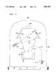
- FIG. 4is a schematic of e-beam deposition apparatus used to form a dielectric (e.g., tantalum-aluminum oxide) coating on the surface of the device of FIG. 1 in accordance with yet another embodiment of our invention.
- a dielectrice.g., tantalum-aluminum oxide
- an active semiconductor device 10(or a portion thereof) which, by way of example, may be an IC, a laser, an LED or a photodetector.
- Device 10may have one or more dielectric coatings 12, 14, formed on one or more surfaces, or facets 16, 18.
- the coatings 12, 14may serve to alter the reflectivity of the surfaces, to passivate them, or both.
- device 10comprises a compound semiconductor material such as a Group III--V or Group II-VI compound material.
- device 10may comprise an elemental semiconductor, such as Si, or a complex, multilayered structure including semiconductor, dielectric and metallic materials (as in the case of a Si IC).
- device 10hereinafter as an InP-InGaAsP multi-quantum well (MQW) distributed feedback (DFB) laser in which case one of the coatings is a high reflectivity (HR) coating 12 and the other is a low reflectivity or anti-reflection (AR) coating 14.
- MQWmulti-quantum well
- HRhigh reflectivity
- ARanti-reflection
- FIG. 2A schematic illustration of such a laser is shown in FIG. 2 where elements corresponding to those of FIG. 1 have been given like reference numbers.
- the laseris mounted on a support member 24 and embedded in an encapsulation material 28 (e.g., a polymer such as an epoxy).
- encapsulation material 28e.g., a polymer such as an epoxy.
- This type of encapsulationis used in non-hermetic packages preferred for low cost applications.
- the basic laser structureis well known in the art; it comprises an MQW active region 20 disposed between a pair of wider bandgap InP cladding regions 22 and 24.
- region 20, as well as the DFB gratingshave been omitted for simplicity. Both are well known to those skilled in the art.
- An HR coating 12is formed on one laser facet, and an AR coating 14 is formed on the other.
- the AR coating 14is a single layer comprising an oxide of tantalum and aluminum.
- the chemical formula for the oxidemay be written as (Al 2 O 3 ) x (Ta 2 O 5 ) 1-x , where x is the mole fraction of Al 2 O 3 in the layer.
- xis the mole fraction of Al 2 O 3 in the layer.
- x ⁇ 0representing essentially no aluminum oxide
- n ox ⁇ 2.1over the same wavelength range.
- n ox⁇ n eff
- n effis the effective refractive index of the surface on which the coating is formed.
- the surfaceis a laser facet formed by the edges of multiple layers of InP and InGaAsP.
- n effis essentially an average of the refractive indices of the layers penetrated by the transverse mode of the laser radiation.
- FIG. 4is a schematic of illustrative apparatus 100 used in such a fabrication process.
- the apparatuscomprises a vacuum chamber 102 in which are disposed: a sample holder 104 which is rotable about an axis 106, a crucible 108 for carrying a source material 110, an ion gun 112, and an e-beam gun 114.
- Holder 104has oblique panels 103, 105 on which samples 101, 107 are mounted. Two panels with four samples each are shown for purposes of illustration only. The samples are illustratively individual semiconductor chips or elongated bars of chips which haven't been separated from one another (in the latter case FIG. 4 would depict such bars end-on).
- the source material 110is heated by an e-beam 115 from gun 114 to a sufficiently high temperature to evaporate the source material.
- the evaporated materialforms a beam 111 which is incident on the samples 101, 107 at all times.
- the ion gun 112generates an ion beam 113 which, in the position shown, is incident on samples 107 but not on samples 101.
- the ion beamis incident on samples 101 but not on 107.
- the samples"see" the ion beam for only a fraction of the cycle time (defined by the rotation speed of the holder).
- the ion beamis effectively pulsed.
- Other techniques for pulsing the ion-beamare also contemplated within the scope of this aspect of our invention; e.g., shuttering the ion gun 112 at a suitable rate (with or without rotation of sample holder 104).
- the reproducibility (e.g., of the refractive index) of the coatingsis improved by filling the crucible 108 with source material 110 in stages; i.e., by repeating a two-step sequence of partially filling the crucible and then premelting the source material.
- the tantalum-aluminum oxide source materialis prepared in granular form by a well known process of ball melting a mixture of tantalum oxide and aluminum oxide in requisite proportion and then sintering the mixture.
- a first quantity (e.g., by weight) of source materialis placed in the crucible.
- the first quantitywhich is insufficient to fill the crucible, is then melted (e.g., by heating it to around 2200° C., illustratively by means of the e-beam 115).
- a second quantity of source materialis added to the first quantity.
- the first and second quantitiesmay be equal to one another, or may be different. Both quantities are likewise heated and melted using the e-beam. This sequence is repeated until the crucible is full or nearly full. The number of repetitions depends on the size of the crucible and the size of quantities and can easily be determined by those skilled in the art.
- One object of this approachis to reduce the shadowing effect caused by the top edges of the crucible; i.e., if the crucible is simply filled in a single step with granular material without using the sequential filling process described above, the top surface tends to sink causing the evaporant beam to be partially blocked by the edges of the crucible. This shadowing effect causes nonuniformity in the thickness of the coatings deposited on the samples.
- e-beam voltagesof about 7 kV, but 5-10 kV is suitable.
- an ion gun voltageof 500 V with 300-700 V being suitable and an ion beam current of 35 mA with 35-100 mA being suitable.
- the ion specieswere Ar ions, although O 2 , Xe, Ne or other ions may also be suitable.
- the pressure in the vacuum chamber 102was typically 1 ⁇ 10 -5 torr to 1 ⁇ 10 -4 torr, although pressures outside this range may also be used. Under these conditions, the deposition rate of 2-10 ⁇ /s is readily achievable, with 2-8 ⁇ /s being typical, and coatings of essentially any desired thickness can be obtained. For example, we have deposited layers of 1000-3000 ⁇ thickness at different deposition rates ranging from 2 to 4 ⁇ /s.
- These layersmay serve as single layer AR coatings (reflectivity ⁇ 1.0%), as low reflectivity (LR) coatings (reflectivity in the range of about 1-10%), or as passivation coatings. In the latter case, if it is desirable not to change the reflectivity of the underlying surface on which the coating is deposited, then the coating thickness should be 2t qw . As noted earlier, for stability in the presence of moisture, it is preferable that 0 ⁇ x ⁇ 0.80.
- the following exampleillustrates how the inventive concepts described above have been applied to depositing tantalum-aluminum oxide AR coatings on the output facets of InP-InGaAsP MQW DFB lasers.
- the laser operating wavelengthwas about 1.3 ⁇ m, and the effective refractive index of the output facet was about 3.24.
- a single layer AR coating of (Al 2 O 3 ) 0 .8 (Ta 2 O 5 ) 0 .2was deposited on the output facet of each laser.
- the refractive index of the coatingswas n ox ⁇ 1.80, and their thickness was about 1800 ⁇ (equal to the quarter wave thickness at ⁇ 1.3 ⁇ m). Note, for a laser operating at, say, 1.55 ⁇ m (n eff ⁇ 3.17), than n ox ⁇ 1.78. Moreover, if the lasers had been encapsulated in a polymer, the corresponding n ox would be higher.
- the coatingswere first tested by immersing them in hot water (96°-99° C.) for 1000 hours. No change in coating thickness or refractive index was observed. Then similar coatings on laser facets (of 1.3 ⁇ m lasers as described above) were stress tested under conditions of 85° C./85% relative humidity and 35 mA of drive current for in excess of 1000 hours. No degradation of laser operation was observed.
- these examplesdemonstrate that we have been able to fabricate reproducible, stable single-layer AR coatings on InP-InGaAsP laser facets, and that the coatings sufficiently passivate the facets to enable the lasers to be operated in a non-hermetic environment.
Landscapes
- Physics & Mathematics (AREA)
- Condensed Matter Physics & Semiconductors (AREA)
- General Physics & Mathematics (AREA)
- Electromagnetism (AREA)
- Optics & Photonics (AREA)
- Semiconductor Lasers (AREA)
- Led Devices (AREA)
- Surface Treatment Of Optical Elements (AREA)
Abstract
Description
Claims (13)
Priority Applications (4)
| Application Number | Priority Date | Filing Date | Title |
|---|---|---|---|
| US08/758,630US5802091A (en) | 1996-11-27 | 1996-11-27 | Tantalum-aluminum oxide coatings for semiconductor devices |
| DE69709042TDE69709042T2 (en) | 1996-11-27 | 1997-11-25 | Semiconductor components coated with tantalum aluminum oxide |
| JP32353797AJP3538302B2 (en) | 1996-11-27 | 1997-11-25 | Optical devices and integrated circuits |
| EP97309473AEP0845839B1 (en) | 1996-11-27 | 1997-11-25 | Semiconductor devices with tantalum-aluminium oxide coating |
Applications Claiming Priority (1)
| Application Number | Priority Date | Filing Date | Title |
|---|---|---|---|
| US08/758,630US5802091A (en) | 1996-11-27 | 1996-11-27 | Tantalum-aluminum oxide coatings for semiconductor devices |
Publications (1)
| Publication Number | Publication Date |
|---|---|
| US5802091Atrue US5802091A (en) | 1998-09-01 |
Family
ID=25052483
Family Applications (1)
| Application Number | Title | Priority Date | Filing Date |
|---|---|---|---|
| US08/758,630Expired - LifetimeUS5802091A (en) | 1996-11-27 | 1996-11-27 | Tantalum-aluminum oxide coatings for semiconductor devices |
Country Status (4)
| Country | Link |
|---|---|
| US (1) | US5802091A (en) |
| EP (1) | EP0845839B1 (en) |
| JP (1) | JP3538302B2 (en) |
| DE (1) | DE69709042T2 (en) |
Cited By (25)
| Publication number | Priority date | Publication date | Assignee | Title |
|---|---|---|---|---|
| US6320265B1 (en) | 1999-04-12 | 2001-11-20 | Lucent Technologies Inc. | Semiconductor device with high-temperature ohmic contact and method of forming the same |
| US6489659B2 (en) | 2000-04-20 | 2002-12-03 | Agere Systems Inc. | Non-hermetic APD |
| US20030021311A1 (en)* | 2001-07-25 | 2003-01-30 | The Furukawa Electric Co., Ltd. | Semiconductor laser module, optical measuring method and optical measuring apparatus |
| US20030059195A1 (en)* | 2001-08-29 | 2003-03-27 | Brennan James F. | Optical devices using shaped optical fibers and methods for making optical devices with shaped optical fibers |
| US20030118918A1 (en)* | 2001-12-21 | 2003-06-26 | Masayuki Ohta | Photomask, production method of semiconductor laser element, and semiconductor laser element |
| US6734036B2 (en)* | 2000-01-18 | 2004-05-11 | Agere Systems Inc. | Semiconductor device and method of fabrication |
| US20040136426A1 (en)* | 2003-01-13 | 2004-07-15 | Widjaja Wilson H. | Moisture passivated planar index-guided VCSEL |
| US20050013993A1 (en)* | 2003-07-16 | 2005-01-20 | Honeywell International Inc. | Environmental & thermal barrier coating |
| US20060249847A1 (en)* | 2005-05-03 | 2006-11-09 | Rosemount Aerospace Inc. | Substrate with bonding metallization |
| KR100653320B1 (en)* | 2003-04-23 | 2006-12-04 | 미쓰비시덴키 가부시키가이샤 | Semiconductor laser device |
| US20070013014A1 (en)* | 2005-05-03 | 2007-01-18 | Shuwen Guo | High temperature resistant solid state pressure sensor |
| US20080121923A1 (en)* | 2006-09-26 | 2008-05-29 | Osram Opto Semiconductors Gmbh | Method for producing an optoelectronic component, and an optoelectronic component |
| US20090108382A1 (en)* | 2005-05-03 | 2009-04-30 | Odd Harald Steen Eriksen | Transducer for use in harsh environments |
| US7628309B1 (en) | 2005-05-03 | 2009-12-08 | Rosemount Aerospace Inc. | Transient liquid phase eutectic bonding |
| CN101621106B (en)* | 2009-07-30 | 2012-05-16 | 中国计量学院 | LED with antireflection film and preparation method thereof |
| DE102014102360A1 (en)* | 2014-02-24 | 2015-08-27 | Osram Opto Semiconductors Gmbh | laser diode chip |
| US10224359B2 (en) | 2012-03-22 | 2019-03-05 | Sionyx, Llc | Pixel isolation elements, devices and associated methods |
| US10229951B2 (en) | 2010-04-21 | 2019-03-12 | Sionyx, Llc | Photosensitive imaging devices and associated methods |
| US10244188B2 (en) | 2011-07-13 | 2019-03-26 | Sionyx, Llc | Biometric imaging devices and associated methods |
| US10269861B2 (en) | 2011-06-09 | 2019-04-23 | Sionyx, Llc | Process module for increasing the response of backside illuminated photosensitive imagers and associated methods |
| US10347682B2 (en) | 2013-06-29 | 2019-07-09 | Sionyx, Llc | Shallow trench textured regions and associated methods |
| US10361083B2 (en) | 2004-09-24 | 2019-07-23 | President And Fellows Of Harvard College | Femtosecond laser-induced formation of submicrometer spikes on a semiconductor substrate |
| US10374109B2 (en) | 2001-05-25 | 2019-08-06 | President And Fellows Of Harvard College | Silicon-based visible and near-infrared optoelectric devices |
| US10505054B2 (en) | 2010-06-18 | 2019-12-10 | Sionyx, Llc | High speed photosensitive devices and associated methods |
| US11239058B2 (en) | 2018-07-11 | 2022-02-01 | Applied Materials, Inc. | Protective layers for processing chamber components |
Families Citing this family (6)
| Publication number | Priority date | Publication date | Assignee | Title |
|---|---|---|---|---|
| EP1198040A1 (en)* | 2000-09-29 | 2002-04-17 | Agere Systems Optoelectronics Guardian Corporation | Optical devices including high reflectivity coatings |
| DE10048475C2 (en) | 2000-09-29 | 2003-04-17 | Lumics Gmbh | Passivation of the resonator end faces of semiconductor lasers based on III-V semiconductor material |
| DE102006054069A1 (en)* | 2006-09-26 | 2008-03-27 | Osram Opto Semiconductors Gmbh | Method for production of opto-electronic component, involves initializing semiconductor layer sequence with active area, where active area is suitable to send electromagnetic radiation in operation |
| DE102007059538B4 (en)* | 2007-12-11 | 2009-08-20 | Lumics Gmbh | Passivation of a resonator end face of a semiconductor laser with a semiconductor superlattice |
| US8355421B2 (en) | 2009-09-16 | 2013-01-15 | Furukawa Electric Co., Ltd | Vertical-cavity surface emitting laser |
| CN108479326B (en)* | 2018-03-12 | 2020-10-16 | 东北师范大学 | Mutually vertical electron beam reflection resonance avalanche desulfurization system |
Citations (3)
| Publication number | Priority date | Publication date | Assignee | Title |
|---|---|---|---|---|
| US4372987A (en)* | 1980-03-12 | 1983-02-08 | D. Swarovski & Co. | Method of producing a multilayer anti-reflection coating |
| US4749255A (en)* | 1985-12-09 | 1988-06-07 | American Telephone And Telegraph Company, At&T Bell Laboratories | Coating for optical devices |
| US5144635A (en)* | 1990-06-19 | 1992-09-01 | Kabushiki Kaisha Toshiba | Semiconductor laser device having reflectance control film formed on end facet of oscillator |
Family Cites Families (4)
| Publication number | Priority date | Publication date | Assignee | Title |
|---|---|---|---|---|
| JPS5832778B2 (en)* | 1979-10-22 | 1983-07-15 | 株式会社東芝 | semiconductor equipment |
| JPH0793474B2 (en)* | 1988-03-01 | 1995-10-09 | 松下電器産業株式会社 | Semiconductor laser device |
| JP3483581B2 (en)* | 1991-08-26 | 2004-01-06 | 株式会社半導体エネルギー研究所 | Semiconductor device |
| US5440575A (en)* | 1994-04-06 | 1995-08-08 | At&T Corp. | Article comprising a semiconductor laser with stble facet coating |
- 1996
- 1996-11-27USUS08/758,630patent/US5802091A/ennot_activeExpired - Lifetime
- 1997
- 1997-11-25DEDE69709042Tpatent/DE69709042T2/ennot_activeExpired - Lifetime
- 1997-11-25EPEP97309473Apatent/EP0845839B1/ennot_activeExpired - Lifetime
- 1997-11-25JPJP32353797Apatent/JP3538302B2/ennot_activeExpired - Fee Related
Patent Citations (3)
| Publication number | Priority date | Publication date | Assignee | Title |
|---|---|---|---|---|
| US4372987A (en)* | 1980-03-12 | 1983-02-08 | D. Swarovski & Co. | Method of producing a multilayer anti-reflection coating |
| US4749255A (en)* | 1985-12-09 | 1988-06-07 | American Telephone And Telegraph Company, At&T Bell Laboratories | Coating for optical devices |
| US5144635A (en)* | 1990-06-19 | 1992-09-01 | Kabushiki Kaisha Toshiba | Semiconductor laser device having reflectance control film formed on end facet of oscillator |
Non-Patent Citations (2)
| Title |
|---|
| Medium Index Mixed Oxide Layers for Use in AR Coatings, SPIE, vol. 662, Thin Film Technologies (1986) Peter Ganner, pp. 69 76 (No Month).* |
| Medium-Index Mixed Oxide Layers for Use in AR-Coatings, SPIE, vol. 662, Thin Film Technologies (1986) Peter Ganner, pp. 69-76 (No Month). |
Cited By (43)
| Publication number | Priority date | Publication date | Assignee | Title |
|---|---|---|---|---|
| US6320265B1 (en) | 1999-04-12 | 2001-11-20 | Lucent Technologies Inc. | Semiconductor device with high-temperature ohmic contact and method of forming the same |
| US6734036B2 (en)* | 2000-01-18 | 2004-05-11 | Agere Systems Inc. | Semiconductor device and method of fabrication |
| US6489659B2 (en) | 2000-04-20 | 2002-12-03 | Agere Systems Inc. | Non-hermetic APD |
| US10374109B2 (en) | 2001-05-25 | 2019-08-06 | President And Fellows Of Harvard College | Silicon-based visible and near-infrared optoelectric devices |
| US6901095B2 (en)* | 2001-07-25 | 2005-05-31 | The Furukawa Electric Co., Ltd. | Semiconductor laser module, optical measuring method and optical measuring apparatus |
| US20030021311A1 (en)* | 2001-07-25 | 2003-01-30 | The Furukawa Electric Co., Ltd. | Semiconductor laser module, optical measuring method and optical measuring apparatus |
| US20030059195A1 (en)* | 2001-08-29 | 2003-03-27 | Brennan James F. | Optical devices using shaped optical fibers and methods for making optical devices with shaped optical fibers |
| US7016387B2 (en)* | 2001-12-21 | 2006-03-21 | Sharp Kabushiki Kaisha | Semiconductor laser element produced by aligning a photomask to pattern an electrode portion superposed on inner portions of upper surfaces of window regions at opposite end faces |
| US20030118918A1 (en)* | 2001-12-21 | 2003-06-26 | Masayuki Ohta | Photomask, production method of semiconductor laser element, and semiconductor laser element |
| US6819697B2 (en)* | 2003-01-13 | 2004-11-16 | Agilent Technologies, Inc. | Moisture passivated planar index-guided VCSEL |
| US20040136426A1 (en)* | 2003-01-13 | 2004-07-15 | Widjaja Wilson H. | Moisture passivated planar index-guided VCSEL |
| KR100653320B1 (en)* | 2003-04-23 | 2006-12-04 | 미쓰비시덴키 가부시키가이샤 | Semiconductor laser device |
| US20050013993A1 (en)* | 2003-07-16 | 2005-01-20 | Honeywell International Inc. | Environmental & thermal barrier coating |
| US10741399B2 (en) | 2004-09-24 | 2020-08-11 | President And Fellows Of Harvard College | Femtosecond laser-induced formation of submicrometer spikes on a semiconductor substrate |
| US10361083B2 (en) | 2004-09-24 | 2019-07-23 | President And Fellows Of Harvard College | Femtosecond laser-induced formation of submicrometer spikes on a semiconductor substrate |
| US7642115B2 (en) | 2005-05-03 | 2010-01-05 | Rosemount Aerospace Inc. | Method for making a transducer |
| US20090108382A1 (en)* | 2005-05-03 | 2009-04-30 | Odd Harald Steen Eriksen | Transducer for use in harsh environments |
| US7538401B2 (en) | 2005-05-03 | 2009-05-26 | Rosemount Aerospace Inc. | Transducer for use in harsh environments |
| US20090203163A1 (en)* | 2005-05-03 | 2009-08-13 | Odd Harald Steen Eriksen | Method for making a transducer |
| US7628309B1 (en) | 2005-05-03 | 2009-12-08 | Rosemount Aerospace Inc. | Transient liquid phase eutectic bonding |
| US7400042B2 (en) | 2005-05-03 | 2008-07-15 | Rosemount Aerospace Inc. | Substrate with adhesive bonding metallization with diffusion barrier |
| US20100047491A1 (en)* | 2005-05-03 | 2010-02-25 | Rosemount Aerospace Inc. | Transient liquid phase eutectic bonding |
| US20100065934A1 (en)* | 2005-05-03 | 2010-03-18 | Odd Harald Steen Eriksen | Transducer |
| US7952154B2 (en) | 2005-05-03 | 2011-05-31 | Rosemount Aerospace Inc. | High temperature resistant solid state pressure sensor |
| US8013405B2 (en) | 2005-05-03 | 2011-09-06 | Rosemount Aerospsace Inc. | Transducer with fluidly isolated connection |
| US20060249847A1 (en)* | 2005-05-03 | 2006-11-09 | Rosemount Aerospace Inc. | Substrate with bonding metallization |
| US8460961B2 (en) | 2005-05-03 | 2013-06-11 | Rosemount Aerospace Inc. | Method for forming a transducer |
| US20070013014A1 (en)* | 2005-05-03 | 2007-01-18 | Shuwen Guo | High temperature resistant solid state pressure sensor |
| US9431580B2 (en)* | 2006-09-26 | 2016-08-30 | Osram Opto Semiconductors Gmbh | Method for producing an optoelectronic component, and an optoelectronic component |
| US20080121923A1 (en)* | 2006-09-26 | 2008-05-29 | Osram Opto Semiconductors Gmbh | Method for producing an optoelectronic component, and an optoelectronic component |
| CN101621106B (en)* | 2009-07-30 | 2012-05-16 | 中国计量学院 | LED with antireflection film and preparation method thereof |
| US10229951B2 (en) | 2010-04-21 | 2019-03-12 | Sionyx, Llc | Photosensitive imaging devices and associated methods |
| US10505054B2 (en) | 2010-06-18 | 2019-12-10 | Sionyx, Llc | High speed photosensitive devices and associated methods |
| US10269861B2 (en) | 2011-06-09 | 2019-04-23 | Sionyx, Llc | Process module for increasing the response of backside illuminated photosensitive imagers and associated methods |
| US10244188B2 (en) | 2011-07-13 | 2019-03-26 | Sionyx, Llc | Biometric imaging devices and associated methods |
| US10224359B2 (en) | 2012-03-22 | 2019-03-05 | Sionyx, Llc | Pixel isolation elements, devices and associated methods |
| US10347682B2 (en) | 2013-06-29 | 2019-07-09 | Sionyx, Llc | Shallow trench textured regions and associated methods |
| US11069737B2 (en) | 2013-06-29 | 2021-07-20 | Sionyx, Llc | Shallow trench textured regions and associated methods |
| CN106063058B (en)* | 2014-02-24 | 2019-03-05 | 欧司朗光电半导体有限公司 | The laser diode chip of laser end face with coating |
| DE102014102360A1 (en)* | 2014-02-24 | 2015-08-27 | Osram Opto Semiconductors Gmbh | laser diode chip |
| CN106063058A (en)* | 2014-02-24 | 2016-10-26 | 欧司朗光电半导体有限公司 | Laser diode chip having coated laser facet |
| US11695251B2 (en) | 2014-02-24 | 2023-07-04 | Osram Oled Gmbh | Laser diode chip having coated laser facet |
| US11239058B2 (en) | 2018-07-11 | 2022-02-01 | Applied Materials, Inc. | Protective layers for processing chamber components |
Also Published As
| Publication number | Publication date |
|---|---|
| JPH10173295A (en) | 1998-06-26 |
| JP3538302B2 (en) | 2004-06-14 |
| DE69709042D1 (en) | 2002-01-24 |
| EP0845839A1 (en) | 1998-06-03 |
| DE69709042T2 (en) | 2002-08-01 |
| EP0845839B1 (en) | 2001-12-12 |
Similar Documents
| Publication | Publication Date | Title |
|---|---|---|
| US5802091A (en) | Tantalum-aluminum oxide coatings for semiconductor devices | |
| EP0674017B1 (en) | Gallium oxide coatings for opto-electronic devices | |
| US4317086A (en) | Passivation and reflector structure for electroluminescent devices | |
| US5851849A (en) | Process for passivating semiconductor laser structures with severe steps in surface topography | |
| CN103107481B (en) | Lasing light emitter | |
| US7600881B2 (en) | Semiconductor light emitting apparatus and its manufacturing method | |
| US4749255A (en) | Coating for optical devices | |
| US20030020076A1 (en) | Optical semiconductor module, its manufacture, reflection film, its manufacture, and laser and optical devices using reflection film | |
| US20200124770A1 (en) | Anti-reflection film and deep ultraviolet light-emitting device | |
| US20080290356A1 (en) | Reflective Layered System Comprising a Plurality of Layers that are to be Applied to a III/V Compound Semiconductor Material | |
| US8368098B2 (en) | Light emitting device and manufacturing method thereof | |
| US5440575A (en) | Article comprising a semiconductor laser with stble facet coating | |
| Oshikiri et al. | Reflectivity dependence of threshold current in GaInAsP/InP surface emitting laser | |
| EP0845819A1 (en) | Yttrium aluminum oxide coatings for active semiconductor optical devices | |
| CA1115401A (en) | Glass coating for semiconductor optical devices | |
| EP1198040A1 (en) | Optical devices including high reflectivity coatings | |
| Chand et al. | High-reliability 1.3-/spl mu/m InP-based uncooled lasers in nonhermetic packages | |
| JP3470476B2 (en) | Semiconductor light emitting device | |
| JPH11145520A (en) | Semiconductor light-emitting element and its manufacturing method | |
| HK1003439B (en) | Gallium oxide coatings for opto-electronic devices | |
| KR101172555B1 (en) | Reflective layered system comprising a plurality of layers that are to be applied to a iii-v compound semiconductor material | |
| Guina et al. | ANTTI SAARELA ADVANCED ION BEAM SPUTTERING COATINGS FOR HIGH-POWER SEMICONDUCTOR DIODE LASERS | |
| Kim et al. | Lasing characteristics of optical thyristor for optical logic function | |
| Chand et al. | High-reliability nonhermetic 1.3-um InP-based uncooled lasers | |
| Nakamura | Highly reliable operation of InGaAlAs mesa-waveguide photodiodes in humid ambient |
Legal Events
| Date | Code | Title | Description |
|---|---|---|---|
| AS | Assignment | Owner name:LUCENT TECHNOLOGIES, INC., NEW JERSEY Free format text:ASSIGNMENT OF ASSIGNORS INTEREST;ASSIGNORS:CHAKRABARTI, UTPAL KUMAR;GRODKIEWICZ, WILLIAM HENRY;WU, PING;REEL/FRAME:008327/0797;SIGNING DATES FROM 19961025 TO 19961029 | |
| STCF | Information on status: patent grant | Free format text:PATENTED CASE | |
| FEPP | Fee payment procedure | Free format text:PAYOR NUMBER ASSIGNED (ORIGINAL EVENT CODE: ASPN); ENTITY STATUS OF PATENT OWNER: LARGE ENTITY | |
| FPAY | Fee payment | Year of fee payment:4 | |
| AS | Assignment | Owner name:AGERE SYSTEMS INC., PENNSYLVANIA Free format text:ASSIGNMENT OF ASSIGNORS INTEREST;ASSIGNOR:LUCENT TECHNOLOGIES INC.;REEL/FRAME:017555/0484 Effective date:20010130 | |
| FPAY | Fee payment | Year of fee payment:8 | |
| FPAY | Fee payment | Year of fee payment:12 | |
| AS | Assignment | Owner name:DEUTSCHE BANK AG NEW YORK BRANCH, AS COLLATERAL AG Free format text:PATENT SECURITY AGREEMENT;ASSIGNORS:LSI CORPORATION;AGERE SYSTEMS LLC;REEL/FRAME:032856/0031 Effective date:20140506 | |
| AS | Assignment | Owner name:AVAGO TECHNOLOGIES GENERAL IP (SINGAPORE) PTE. LTD Free format text:ASSIGNMENT OF ASSIGNORS INTEREST;ASSIGNOR:AGERE SYSTEMS LLC;REEL/FRAME:035365/0634 Effective date:20140804 | |
| AS | Assignment | Owner name:AGERE SYSTEMS LLC, PENNSYLVANIA Free format text:TERMINATION AND RELEASE OF SECURITY INTEREST IN PATENT RIGHTS (RELEASES RF 032856-0031);ASSIGNOR:DEUTSCHE BANK AG NEW YORK BRANCH, AS COLLATERAL AGENT;REEL/FRAME:037684/0039 Effective date:20160201 Owner name:LSI CORPORATION, CALIFORNIA Free format text:TERMINATION AND RELEASE OF SECURITY INTEREST IN PATENT RIGHTS (RELEASES RF 032856-0031);ASSIGNOR:DEUTSCHE BANK AG NEW YORK BRANCH, AS COLLATERAL AGENT;REEL/FRAME:037684/0039 Effective date:20160201 | |
| AS | Assignment | Owner name:BANK OF AMERICA, N.A., AS COLLATERAL AGENT, NORTH CAROLINA Free format text:PATENT SECURITY AGREEMENT;ASSIGNOR:AVAGO TECHNOLOGIES GENERAL IP (SINGAPORE) PTE. LTD.;REEL/FRAME:037808/0001 Effective date:20160201 Owner name:BANK OF AMERICA, N.A., AS COLLATERAL AGENT, NORTH Free format text:PATENT SECURITY AGREEMENT;ASSIGNOR:AVAGO TECHNOLOGIES GENERAL IP (SINGAPORE) PTE. LTD.;REEL/FRAME:037808/0001 Effective date:20160201 | |
| AS | Assignment | Owner name:AVAGO TECHNOLOGIES GENERAL IP (SINGAPORE) PTE. LTD., SINGAPORE Free format text:TERMINATION AND RELEASE OF SECURITY INTEREST IN PATENTS;ASSIGNOR:BANK OF AMERICA, N.A., AS COLLATERAL AGENT;REEL/FRAME:041710/0001 Effective date:20170119 Owner name:AVAGO TECHNOLOGIES GENERAL IP (SINGAPORE) PTE. LTD Free format text:TERMINATION AND RELEASE OF SECURITY INTEREST IN PATENTS;ASSIGNOR:BANK OF AMERICA, N.A., AS COLLATERAL AGENT;REEL/FRAME:041710/0001 Effective date:20170119 |