US5801602A - Isolation and signal filter transformer - Google Patents
Isolation and signal filter transformerDownload PDFInfo
- Publication number
- US5801602A US5801602AUS08/641,375US64137596AUS5801602AUS 5801602 AUS5801602 AUS 5801602AUS 64137596 AUS64137596 AUS 64137596AUS 5801602 AUS5801602 AUS 5801602A
- Authority
- US
- United States
- Prior art keywords
- transformer
- trace
- metal trace
- substrate
- primary winding
- Prior art date
- Legal status (The legal status is an assumption and is not a legal conclusion. Google has not performed a legal analysis and makes no representation as to the accuracy of the status listed.)
- Expired - Lifetime
Links
Images


Classifications
- H—ELECTRICITY
- H01—ELECTRIC ELEMENTS
- H01F—MAGNETS; INDUCTANCES; TRANSFORMERS; SELECTION OF MATERIALS FOR THEIR MAGNETIC PROPERTIES
- H01F17/00—Fixed inductances of the signal type
- H01F17/0006—Printed inductances
- H—ELECTRICITY
- H01—ELECTRIC ELEMENTS
- H01F—MAGNETS; INDUCTANCES; TRANSFORMERS; SELECTION OF MATERIALS FOR THEIR MAGNETIC PROPERTIES
- H01F19/00—Fixed transformers or mutual inductances of the signal type
- H01F19/04—Transformers or mutual inductances suitable for handling frequencies considerably beyond the audio range
- H01F19/08—Transformers having magnetic bias, e.g. for handling pulses
- H01F2019/085—Transformer for galvanic isolation
- H—ELECTRICITY
- H03—ELECTRONIC CIRCUITRY
- H03H—IMPEDANCE NETWORKS, e.g. RESONANT CIRCUITS; RESONATORS
- H03H1/00—Constructional details of impedance networks whose electrical mode of operation is not specified or applicable to more than one type of network
- H03H2001/0021—Constructional details
- H03H2001/0078—Constructional details comprising spiral inductor on a substrate
- H—ELECTRICITY
- H03—ELECTRONIC CIRCUITRY
- H03H—IMPEDANCE NETWORKS, e.g. RESONANT CIRCUITS; RESONATORS
- H03H7/00—Multiple-port networks comprising only passive electrical elements as network components
- H03H7/42—Networks for transforming balanced signals into unbalanced signals and vice versa, e.g. baluns
- H03H7/425—Balance-balance networks
- H03H7/427—Common-mode filters
Definitions
- This inventionrelates to the field of communications circuits.
- the inventionrelates to a use of an isolation and filter circuit.
- Isolation circuits and filter circuitsare often used in devices connected to transmission lines.
- the transmission linescarry a signal to the devices or away from the devices.
- a combination isolation and filter circuitis used to transfer and filter a signal from the network cable to the adapter card, or from the adapter card to the network cable.
- the isolation part of the circuitisolates the rest of the adapter card circuitry from the network cable.
- the filter partremoves high frequency components of the signal.
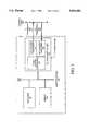
- FIG. 1illustrates two combination isolation and filter circuits 100 as used in a 10 MHz ethernet adapter card.
- the transmit circuit 101transmits signals from the adapter card to the network cable, while the receive circuit 102 receives signals from the network cable and transmits them to the adapter card.
- Part number FL 1012 and FL 1066available from Valor, Inc., implements the isolation and filter circuits 100.
- the transmit circuit 101includes a filter 110, a transformer 120 and a common mode choke circuit 130.
- the filter 110connects to the transmit side of the adapter card electronics and to the transformer 120.
- the transformer 120connects to the common mode choke circuit 130.
- the common mode choke 130connects to the network cable.
- the filter 110includes a number of inductors and capacitor.
- the inductors and capacitorsact as a seven pole filter for signals being transmitted to the network.
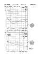
- the frequency response of the transmit circuit 101is shown in FIG. 2.
- the 100 MHz frequency response graph 210shows that the transmit circuit 101 acts as a low pass filter, with a response that quickly rolls off near 16 MHz.
- the 1 GHz frequency response graph 200shows that the transmit circuit 101 does not transmit more than -20 dB for any other frequency between 25 MHz and 1 GHz. For 10 Mbit ethernet communications, such a frequency response is desirable because high frequency noise components of the transmitted signal are removed before the signal is transmitted to the network cable. The frequency response thus allows the adapter card to meet electromagnetic interference requirements.
- the transformer 120electrically isolates the adapter card from the network cable.
- the transformer 120has a relatively good frequency response. That is, both high frequencies (e.g., 800 MHz) and low frequencies (20 kHz) are passed through the transformer 120 with little attenuation.
- the common mode choke 130is part of the filter 110 and helps to remove high frequency components from the signal being sent to the network cable.
- the receive circuit 102includes circuits similar to those in the transmit circuit 101. However, the receive filter 112 has fewer inductors and capacitors than the filter 110, resulting in a low pass filter with fewer poles. Having fewer poles means that the receive filter 112 does not have as steep a roll off as the filter 110. Because the receive characteristics are not as stringent as the transmit characteristics, a filter having fewer poles is acceptable. Importantly, reducing the number of inductors and capacitors also reduces the cost of the filter 110.
- isolation and filter circuit 100adds a significant cost to the price of the adapter cards. Thus, it is desirable to have an isolation and filter circuit 100 with a lower cost but still maintain a similar frequency response.
- isolation and filter circuits 100For different communications standards, a different part is needed to implement the different isolation and filter circuits 100. For example, one part will have the desired frequency response for 10 Mbit ethernet, while another part will have the desired frequency response for 16 MHz token ring. Maintaining an inventory of all these different parts is expensive because the individual cost of each of the parts is relatively expensive. Therefore, it is desirable to have a more versatile isolation and filter circuit 100.
- One embodiment of the inventionincludes a transformer that is at least partially formed on a substrate.
- the transformeris for electrical isolation and signal filtering.
- the transformerincludes the following elements.
- a portion of the substratehas two holes through the substrate.
- a ferrite coreis formed in a loop through the two holes.
- a primary windingis made of a first metal trace.
- the first metal traceis formed in a spiral around one hole.
- the first metal tracehas at least two primary terminals acting as an input to the transformer.
- the transformeralso includes a secondary winding.
- the secondary windingis made of a second metal trace.
- the second metal traceis formed in a spiral around the other hole.
- the second metal tracehas at least two secondary terminals acting as an output from the transformer.
- one embodiment of the inventiongreatly reduces the cost of manufacturing filtering and isolation circuits in network adapter cards, and other communications systems, by integrating the filtering and isolation functions into one structure.
- reactive elementssuch as an external capacitor, are added to further change the frequency response of the transformer.
- the isolation and signal filter transformeris tuned to have a desired frequency response by taking advantage of the parasitic capacitances and inductances of the traces of both the primary and the secondary winding.
- the parasitic capacitances and inductancesare controlled by the layout of these traces.
- FIG. 1illustrates a prior art filter circuit
- FIG. 2a and FIG. 2billustrate the frequency response of the prior art filter of FIG. 1.
- FIG. 3illustrates one embodiment of the invention as used in a network adapter card.
- FIG. 4illustrates a layout of a transformer.
- FIG. 5a and FIG. 5billustrates a linear model of the layout of FIG. 4.
- FIG. 6illustrates an example frequency response of one embodiment of the invention.
- FIG. 7a and FIG. 7billustrate an example frequency response of one embodiment of the invention including an external capacitor.
- FIG. 8a and FIG. 8billustrate an example frequency response of one embodiment of the invention including two external capacitors.
- FIG. 9illustrates a bifilar transformer
- FIG. 10illustrates a multi-layered substrate having an integrated transformer.
- FIG. 3illustrates a network adapter card using one embodiment of the invention.
- FIG. 3includes a computer system 300, with a network adapter card 310, and a network cable 370.
- the network adapter card 310includes two integrated transformers that cost much less than previous combined filter and isolation circuits.
- the two integrated transformershave their windings formed directly on, and/or in, the network adapter card's substrate.
- a ferrite, or other metal, coreis then positioned through the windings, and therefore through the substrate.
- the parasitic characteristics, such as capacitance, inductance, and resistance, of these windings and the coreare used to create a filter.
- the computer system 300includes a processor 380, a memory 390, a bus 399, and the network adapter card 310.
- the processor 380, the memory 390 and the network adapter card 310are all connected to, and communicate over, the bus 399.
- the computer system 300includes one of an IBM PC-compatible computer, a MacintoshTM computer, a Sun SparcstationTM computer, or some other computer having a processor and a memory.
- the network cable 370includes at least one pair, and in the example of FIG. 3, two pairs, of transmission lines.
- the TX (transmit) transmission lines 371communicate signals from the network adapter card 310 to the rest of the network.
- the RX (receive) transmission lines 372communicate signals from the rest of the network to the network adapter card 310.
- the network cable 370includes a 10base-T cable.
- the network cable 370includes one of: an AUI cable, twisted pair FDDI cable, 100base-T cable, and AppleTalkTM cable, or some other type of transmission line medium (e.g., a telephone line).
- the network adapter card 310includes a substrate 360, the TX integrated transformer 321, the RX (receive) integrated transformer 322, and the other adapter electronics 330.
- the TX integrated transformer 321, the RX integrated transformer 322 and the other adapter electronics 330are mounted on, in and/or through the substrate 360. Both of the TX integrated transformer 321 and the RX integrated transformer 322 connect to the other adapter electronics 330.
- the TX integrated transformer 321also connects to the TX transmission lines 371.
- the RX integrated transformer 322connects to the RX transmission lines 372.
- the substrate 360includes a double-sided printed circuit board made of 0.062 ⁇ 0.005 inch thick glass epoxy, natural color, laminated NEMA GRADE FR-4 available from Solectron, Inc. of Milpitas, Calif.
- the substrate 360has a dielectric constant of 4.5 ⁇ 0.4 at 1 MHz, the dielectric strength perpendicular to an adjacent layer has a minimum of 750 VDC per 0.001 inch thickness of the substrate. Traces are formed on, or in the substrate, with 1/2 ounce copper.
- other materialsare used, such as, a printed circuit board having more than two layers of copper, a substrate including a ground plane layer, a 0.075 ⁇ 0.003 thick glass epoxy, or polyamide fiberglass GRADE FR-5.
- Other embodimentsalso have variations in the dielectric constant and the dielectric strength.
- the other adapter electronics 330include the electronics for preparing, sending and/or receiving data over the network cable 370 or the bus 399, and interfacing with the bus 399.
- the other adapter electronics 330includes the circuits for implementing the 10base-T standard, except for those parts of the standard implemented by the integrated transformers.
- the other adapter electronics 330implement other communications standards.
- the computer system 300does not include the network adapter card 310.
- the components on the network adapter card 310are included directly on the motherboard to which the processor 380 and the memory 390 are mounted.
- the integrated transformersare manufactured by forming the windings directly on the substrate and inserting a core through the windings. This process results in a less than ideal transformer. Significant parasitic capacitance, inductance, and resistance are all a result of manufacturing the integrated transformers in this way. However, one embodiment of the invention uses these parasitic characteristics advantageously to create a filter. The filter passes only those parts of a signal that are desired. Thus, the integrated transformers completely, or at least partially, replace the prior art combined isolation and filter circuit 100. This significantly reduces the cost of the network adapter card 310.
- FIG. 4shows a layout of an integrated transformer 400.
- variations of the integrated transformer 400are used as the TX integrated transformer 321 and the RX integrated transformer 322.
- the integrated transformer 400includes two sets of windings, two holes and a ferrite core 450.
- the two sets of windingsinclude the primary winding 410 and the secondary winding 420.
- the primary winding 410is used as a secondary winding
- the secondary winding 420is used as a primary winding.
- the primary winding 410is made of a top trace 412 and a bottom trace 414 that are connected through the substrate 360 by the via 411.
- the secondary winding 420is made of a top trace 422 and a bottom trace 424 that are connected through the substrate 360 by the via 421.
- FIG. 4presents two top views of a portion of the substrate 360 to show the two traces.
- the first top viewshows the top traces formed as spirals, around the holes, on the top surface of the substrate 360.
- the bottom tracesare formed as spirals, around the holes, on the bottom surface of the substrate 360.
- the bottom tracesare formed directly under the top traces.
- the bottom tracesare shown with dashed lines in a second top view. (The second top view shows the bottom traces as one would see the bottom traces if the substrate 360 were transparent and the top traces were removed.)
- the bottom tracesare not directly under the traces. This changes the parasitic characteristics of the integrated transformer (e.g., as described below, Cp1 570 and Ll1 520 for the primary winding 410, and Cp2 575 and Ll2 525 for the secondary winding 420).
- the tracesare made of the same material as is used in the rest of the network adapter card 310.
- the top trace 412, the top trace 422, the bottom trace 414, and the bottom trace 424are made of copper and are formed on the surface of the substrate 360.
- the tracesare made during the manufacturing of the network adapter card 310 and at the same time that traces are made for the other adapter electronics 330.
- the top and bottom tracesare 0.007 ⁇ 0.001 inch wide, having a minimum spacing of 0.008 inches.
- Each holeis made at approximately the center of a winding.
- hole 415is made in the center of the primary winding 410
- hole 425is made in the center of the secondary winding 420.
- each holeis approximately square.
- the holesare approximately round because round holes are less costly to manufacture.
- a ferrite core 450is placed in the holes to form a closed loop.
- the ferrite core 450is made of two pieces of ferrite. The top is a U-shaped ferrite core piece 452. The bottom is an I-shaped ferrite core piece 454. The ends of the U-shaped piece 452 are placed through the holes. The I-shaped piece 454 is then attached to the ends of the U-shaped piece 452 that are protruding through the bottom of the substrate 360. In one embodiment, the I-shaped piece 454 is attached to the U-shaped piece using a clamp. The clamped U-shaped piece 452 and the I-shaped piece 454 form a closed ferrite loop through the primary winding 410 and the secondary winding 420. The closed loop allows the magnetic flux generated from the primary winding 410 to flow through the ferrite core 450. As the magnetic flux passes through the secondary winding 420, a current is induced in the secondary winding 420. Thus, a transformer is formed.
- the ferrite core 450is made of two U-shaped core pieces from Fair-Rite Products Corporation of Wallkill, N.Y., part number 90--002002, made of material 77 (manganese-zinc material).
- the distance between the inner edges of the two holesis slightly less (e.g., 0.005 inches) than 0.09 inches and the distance between the outer edges of the two holes is slightly greater (e.g., 0.005 inches) than 0.34 inches.
- the tracesare 0.007 inches wide.
- the spacing between two adjacent portions of trace materialis 0.008 inches.
- the distance from the edge of a hole to the nearest edge of a traceis approximately 0.01 inches.
- Other embodiments of the inventionuse different sizes and distances depending upon the desired frequency response of the integrated transformer.
- FIG. 4 and the above descriptionshow how an integrated transformer can be built from a few traces, a substrate 360 and a ferrite core 450.
- This integrated transformeris much less expensive than previous isolation and filter circuits, such as the isolation and filter circuit 100.
- the reduced costsare a result of having fewer, lower cost, and more reliable components. For example:
- the additional capacitors and inductors of the circuit 100are not needed to provide the desired signal filtering.
- the transformer 120costs significantly more to build than the integrated transformer because the transformer 120 uses relatively expensive wire windings.
- the integrated transformeris more reliable than the circuit 100 because the integrated transformer requires few, or no, external capacitors and inductors.
- the integrated transformeris built using more reliable technology (e.g., the traces may have better tolerances than the tolerances of the transformer's 120 windings).
- the integrated transformerhas more consistent performance.
- FIG. 5a and FIG. 5billustrate an integrated transformer linear model 500.
- the integrated transformer linear model 500shows how parasitic characteristics are used to change the filtering characteristics of an integrated transformer.
- Table 1shows the devices of the integrated transformer linear model 500.
- Rg1 541connects across the input terminals of the integrated transformer.
- Rs1 510connects in serial to a first input terminal.
- Ll1 520connects to the other terminal of Rs1 510.
- Ll2 525connects to the other terminal of Ll1 520.
- Rs2 515connects to the other terminal of Ll2 525.
- Rg3 542, Lm2 552, Cp2 575, Zl 501 and the primary winding of the ideal transformer 503connect in parallel between the other terminal of Rs2 515 and the second input terminal.
- Lm1 550, Cp1 570 and Rloss 509connect in parallel from the second input terminal and the connection between Ll1 520 and Ll2 525.
- Cc 505 and Rg2 507connect in parallel to the connection between Rs1 510 and Ll1 520 and the connection between Ll2 525 and Rs2 515.
- the secondary winding of the ideal transformer 503connects to the output terminals.
- the leakage inductanceis kept to a minimum. That is, prior art transformers are manufactured to reduce the leakage inductance. The reason for this is that the leakage inductor acts to prevent the transformer from transferring all of the input signal to the output.
- this feature of the leakage inductance, in conjunction with the primary winding's inter-trace capacitance,are advantageously used to filter the received signal.
- the leakage inductance, Ll1 520, and the inter-trace capacitance, Cp1 570are a series resonant circuit that act as a low pass filter.
- the leakage inductance, Ll1 520is varied by varying the distance between the internal edges of the core and the number of turns (greater distance means a greater leakage inductance).
- the inter-trace capacitance, Cp1 570is varied by varying the widths of the primary winding's traces and the distances between these traces.
- the magnetizing inductance, Lm1 550, and the inter-trace capacitance, Cp1 570form a parallel resonant circuit that acts as a band pass filter.
- Lm1 550 and Cp1 570the resonance frequency for this filter can be changed.
- Lm1 550can be varied by changing the materials used to make the ferrite core 450, the shape of the core (e.g., circular, rectangular), the layout of the trace, and the number of turns of the trace.
- Cp1 570is changed in the following ways.
- the substrate 360includes additional layers, such as a ground plane, that can be used to alter Cp1 570.
- Cp1 570is changed by extending trace material from the top trace 412 and/or the bottom trace 414. An example of an extended trace is shown in FIG. 5b as extended trace 588.
- similar extensionsare made on both the primary winding 410 and the secondary winding 420 to vary Cc 505 and Rg2 507.
- the resonant frequency of both of these resonant circuitsis altered so that the integrated transformer passes desirable frequencies and attenuates the other frequencies.
- Table 2shows how some of the manufacturing variables can be changed to alter the values of the integrated transformer.
- the following manufacturing characteristicsare modified: trace width, trace spacing, trace length, winding shape (only in the same approximate planes as the surfaces of the substrate 360), core shape, and core material.
- the characteristics of the trace material and the substrate 360 materialare not altered in this embodiment so that the integrated transformer is made using the same trace material and substrate 360 material as is used by, for example, the other adapter electronics 330. That is, in this embodiment, there is a common set of design rules, for making a printed circuit board, that are used by the integrated transformers and the other adapter electronics 330. These design rule specify which parameters may not be changed (e.g., the substrate 360 material, trace thickness) and which parameters may be changed (e.g., trace width).
- reactive elementssuch as external capacitors and inductors
- reactive elementsare added to the integrated transformer to help achieve a particular frequency response.
- an external capacitor, C 535is included.
- C 535is connected across the input terminals to the integrated transformer.
- C 535is mounted through the via 417 and a new via 517.
- a surface mounted capacitoris used.
- C 535effectively increases Cp1 570.
- C 535is helpful where Cp1 570 cannot be increased to a desired level without undesirably altering other parameters of the model 500.
- C 535is determined so that the band pass filter of Cp1 570, C 535 and Lm1 550 has a frequency response that resonates at 10 MHz.
- C 535 valuesare chosen for other frequencies (e.g., 200 kHz, 4 MHz, 16 MHz, 20 MHz, 100 MHz).
- C 535is determined so that the integrated transformer, as laid out in FIG. 4, has a resonant frequency of 10 MHz.
- C 535is determined as follows.
- Lthe inductance, of the integrated transformer, as measured across the input terminals of the primary winding 410, is determined.
- Lis proportional to Ll1 520 and Lm1 550.
- Lis measured, for a given integrated transformer, from a Smith chart plot, at the 10 MHz point, generated by a 1 GHz Hewlett-Packard Network Analyzer. In the example of FIG. 4, L is approximately 643 nH.
- Cis then determined as follows:
- C 535is approximately 395 pF.
- this integrated transformerwill have a resonant frequency at 10 MHz. (This is shown in FIG. 7a and 7b and described below.)
- FIG. 6illustrates the frequency response of an integrated transformer using the layout of FIG. 4.
- the 1 GHz integrated transformer frequency response graph 600at approximately 10 MHz, the signal has been reduced by 1.2 dB. The signal response then begins to roll off, reaching almost -30 dB by approximately 300 MHz.
- the graph 600illustrates that the parasitic characteristics of the integrated transformer can be used to make the integrated transformer into a filter. By altering the parasitic characteristics greater roll off can be achieved and at the desired frequency.
- Cc 505changes frequency response.
- Cc 505is reduced to help attenuate undesirable high frequency signals.
- Cc 505is reduced by placing a trace connect to ground between the primary winding 410 and the secondary winding 420. In this embodiment, the additional trace to ground also helps increase Cp1 570 and Cp2 575.
- Cc 505is reduced by increasing the distance between the closest trace edge of the primary winding 410 to the closest trace edge of the secondary winding 420.
- One method of increasing Cc 505is to position the primary winding 410 and the secondary winding 420 next to each other to create a bifilar integrated transformer.
- Cc 505acts as a parallel resonant circuit with Ll1 520+Ll2 525, thereby reducing the energy transfer from the input terminals to the output terminals at a certain frequency.
- FIG. 7a and 7billustrate the frequency response of an integrated transformer using the layout of FIG. 4 and including an external capacitor C 535 of approximately 380 pF.
- the signalhas been reduced by only 1.3 dB.
- the signalnow begins to roll off much more quickly than the integrated transformer without the capacitor, reaching -20 dB by 40 MHz.
- the high frequency responseat approximately 800 MHz, is also reduced.
- FIG. 7billustrates that only a small amount of the signal is lost in the 100 kHz to 10 MHz frequency range.
- 10 Mbit ethernet communicationslow signal loss in this frequency range is desirable.
- additional changes in the parasitic characteristics of the integrated transformercause the band stop filter characteristics of Ll1 and Cp1 to have greater effect. This reduces some of the low frequency components of the signal. For some communications protocols, the loss of these frequency components are relatively insignificant.
- FIG. 8a and FIG. 8billustrate the frequency response of the same embodiment of the integrated transformer as in FIG. 7a and 7b, but with the addition of a second external capacitor C2 545.
- C2 545is connected across the output terminals of the integrated transformer to be tuned to the desired frequency response.
- the capacitance of C2 545is determined in a similar manner as C 535.
- C2 545has a capacitance of approximately 380 pF.
- FIG. 8ashows that all of the high frequency signals are attenuated below 20 dB.
- FIG. 8bshows that the important frequency response between five MHz and ten MHz is relatively linear. Additionally, the amount of signal loss has improved to only approximately 0.6 dB at approximately 10 MHz. In particular, compared with the prior art frequency response in graph 220, the frequency response of the embodiment of FIG. 8a and FIG. 8b has less signal loss between five MHz and 10 MHz.
- FIG. 9illustrates a bifilar transformer as can be used in one embodiment of the invention.
- the transformer 910includes a substrate 920, a core 930, a metal trace 940, and a metal trace 950.
- the metal trace 940 and the metal trace 950are formed in a spiral around the core 930. This shape increases the coupling capacitance between the two metal traces.
- FIG. 10illustrates one embodiment of the invention having a transformer 1010 for electrically isolating and filtering a network communications signal.
- the transformer 1010comprises a substrate 1020, a closed loop of ferrite core 1030, a metal trace 1040, and a metal trace 1050.
- the substratehas a hole 1022 and a hole 1024 through the substrate.
- the closed loop of ferrite core 1030is disposed through the hole 1022 and the hole 1024.
- the metal trace 1040is positioned in a spiral around the hole 1022.
- the metal trace 1040is coupled to receive network communications signals.
- the metal trace 1050is positioned in a spiral around the hole 1024 and is coupled to filter and transmit network communications signals.
- the substratehas three layers.
- the metal trace 1040couples the part of the trace on the top layer to the part of the trace on the middle layer.
- the part of the trace on the middle layeris coupled to the part of the trace on the bottom layer.
- the metal trace 1040is positioned to at least increase the coupling capacitance to cause the transformer to attenuate signals above 300 MHz by more than three dB while not attenuating signals at, or near 100 MHz, by more than three dB.
- the abovedescribes many different integrated transformers tuned to provide specific desired frequency responses.
- the integrated transformersgreatly reduce the cost of manufacturing filtering and isolation circuits in network adapter cards, and other communications systems, by integrating the filtering and isolation functions into one structure.
- the integrated transformeris made from traces on a substrate and a ferrite core.
- the same techniques used for forming the traces to connect the rest of the components on the substrateare used to create the traces for the windings of the integrated transformer, thereby reducing the cost of the integrated transformer.
- the parasitic characteristics of the windings and the ferrite coreare modified to advantageously change the frequency response of the integrated transformer.
- external reactive elementssuch as an external capacitor, are added to further change the frequency response of the integrated transformer.
Landscapes
- Engineering & Computer Science (AREA)
- Power Engineering (AREA)
- Multimedia (AREA)
- Microelectronics & Electronic Packaging (AREA)
- Coils Or Transformers For Communication (AREA)
- Filters And Equalizers (AREA)
- Cable Transmission Systems, Equalization Of Radio And Reduction Of Echo (AREA)
Abstract
Description
TABLE 1 ______________________________________ Label Description ______________________________________Rs1 510 Series resistance of the entire primary winding 410 (top trace 412 resistance plusbottom trace 414 resistance). Ll1 520 Leakage inductance of the primary winding 410.Lm1 550 Magnetizing inductance of the primary winding 410.Cp1 570 Inter-trace capacitance of the primary winding 410 (as shown in FIG. 5b and also between thetop trace 412 and the bottom trace 414).Rs2 515 Series resistance of the entire secondary winding 420 (top trace 422 resistance plusbottom trace 424 resistance).Ll2 525 Leakage inductance of the secondary winding 420.Cp2 575 Inter-trace capacitance of the secondary winding 420 (as shown in FIG. 5b and also as between thetop trace 422 and the bottom trace 424).Zl 501 Impedance of the load connected to the output of the secondary winding 420. Ideal An ideal transformer with a transformer ratio ofTransformer 503 1:1. (Although other ratios are used in other embodiments where the output voltage needs to be stepped up or stepped down.)Cc 505 Capacitive coupling between the primary winding 410 and the secondary winding 420.Rg1 541 Resistance between the primary winding 410 input terminals. The resistance is due to the conductivity of the dielectric material used as thesubstrate 360.Rg2 507 Resistance of dielectric material between the primary winding 410 and the secondary winding 420.Rg3 542 Resistance between the secondary winding 420 output terminals. The resistance is due to the conductivity of the dielectric material used as thesubstrate 360.Rloss 509 Resistance of theferrite core 450. This is due to a heating of the core when transferring a signal from the primary winding 410 to the secondary winding 420. ______________________________________
TABLE 2 ______________________________________ Label Dependencies ______________________________________Rs1 510 Directly proportional to the length of the primary winding 410. Each additional length of the trace material adds to the resistance of the primary winding. Inversely proportional to the width and depth of the primary winding 410. Also depends on the resistance of the trace material used. Ll1 520 Depends upon the distance between the internal edges of the core, the physical layout of the trace, and the number of turns.Lm1 550 Directly proportional to the number of turns in the primary winding 410. Depends upon the properties of theferrite core 450, such as its shape and composition (i.e. composition of metal). Also depends upon the frequency of input signal, the layout of the trace, and the number of turns.Lm2 552 Directly proportional to the number of turns in the secondary winding 420. Depends upon the properties of theferrite core 450, such as its shape and composition (i.e. composition of metal). Also depends upon the frequency of input signal, the layout of the trace, and the number of turns.Cp1 570 Inversely proportional to the distance between the traces of the primary winding 410. This includes the distance between two adjacent lengths of thetop trace 412 and the distance between thetop trace 412 and thebottom trace 414. In one embodiment, the top trace is displaced from thebottom trace 414 to alterCp1 570. Also depends upon the trace material used and the dielectric characteristics of thesubstrate 360 material.Rs2 515 Similar toRs1 510 except for the secondary winding 420.Ll2 525 Similar to Ll1 520 except for the secondary winding 420.Cp2 575 Similar to Cp1 570 except for the secondary winding 420.Cc 505 Inversely proportional to the distance between the edges of the primary winding 410 and the secondary winding 420. Depends on the trace material used and the dielectric characteristics of thesubstrate 360 material. Depends also on the relative trace positioning of the primary winding 410 and the secondary winding 420. The windings are shown adjacent to each other in FIG. 4, however, in one embodiment, a bifilar transformer is formed by forming the traces of the two windings next to each other.Rg1 541 Directly proportional to the distance between the edges of the primary winding 410 traces. Also depends upon the resistance of the dielectric material used as part of thesubstrate 360.Rg2 507 Directly proportional to the distance between the edges of the primary winding 410 and secondary winding 420. Also depends upon the resistance of the dielectric material.Rg3 542 Directly proportional to the distance between the edges of the secondary winding 420 traces. Also depends upon the resistance of the dielectric material used as part of thesubstrate 360.Rloss 509 Depends upon the core material being used as well as the input signal excitation (e.g., frequency and voltage). ______________________________________
Claims (17)
Priority Applications (4)
| Application Number | Priority Date | Filing Date | Title |
|---|---|---|---|
| US08/641,375US5801602A (en) | 1996-04-30 | 1996-04-30 | Isolation and signal filter transformer |
| PCT/US1997/004749WO1997041639A1 (en) | 1996-04-30 | 1997-03-25 | Isolation and signal filter transformer |
| TW086104608ATW318247B (en) | 1996-04-30 | 1997-04-10 | Isolation and signal filter transformer |
| US09/075,373US6049258A (en) | 1996-04-30 | 1998-05-11 | Isolation and signal filter transformer |
Applications Claiming Priority (1)
| Application Number | Priority Date | Filing Date | Title |
|---|---|---|---|
| US08/641,375US5801602A (en) | 1996-04-30 | 1996-04-30 | Isolation and signal filter transformer |
Related Child Applications (1)
| Application Number | Title | Priority Date | Filing Date |
|---|---|---|---|
| US09/075,373Continuation-In-PartUS6049258A (en) | 1996-04-30 | 1998-05-11 | Isolation and signal filter transformer |
Publications (1)
| Publication Number | Publication Date |
|---|---|
| US5801602Atrue US5801602A (en) | 1998-09-01 |
Family
ID=24572090
Family Applications (2)
| Application Number | Title | Priority Date | Filing Date |
|---|---|---|---|
| US08/641,375Expired - LifetimeUS5801602A (en) | 1996-04-30 | 1996-04-30 | Isolation and signal filter transformer |
| US09/075,373Expired - LifetimeUS6049258A (en) | 1996-04-30 | 1998-05-11 | Isolation and signal filter transformer |
Family Applications After (1)
| Application Number | Title | Priority Date | Filing Date |
|---|---|---|---|
| US09/075,373Expired - LifetimeUS6049258A (en) | 1996-04-30 | 1998-05-11 | Isolation and signal filter transformer |
Country Status (3)
| Country | Link |
|---|---|
| US (2) | US5801602A (en) |
| TW (1) | TW318247B (en) |
| WO (1) | WO1997041639A1 (en) |
Cited By (61)
| Publication number | Priority date | Publication date | Assignee | Title |
|---|---|---|---|---|
| US6049258A (en)* | 1996-04-30 | 2000-04-11 | 3Com Corporation | Isolation and signal filter transformer |
| US6147576A (en)* | 1998-04-10 | 2000-11-14 | Ameramp Llc | Filter designs utilizing parasitic and field effects |
| US6147928A (en)* | 1998-03-10 | 2000-11-14 | Tdk Corporation | Anti-noise component for flat cable |
| US6177851B1 (en)* | 1998-05-06 | 2001-01-23 | Alps Electric Co., Ltd. | High-frequency electronic device |
| US6255714B1 (en)* | 1999-06-22 | 2001-07-03 | Agere Systems Guardian Corporation | Integrated circuit having a micromagnetic device including a ferromagnetic core and method of manufacture therefor |
| US6366180B1 (en)* | 1998-11-20 | 2002-04-02 | Deutsche Thomson-Brandt Gmbh | Mains filter |
| US20020112070A1 (en)* | 2000-12-08 | 2002-08-15 | The Boeing Company | Network controller for digitally controlling remote devices via a common bus |
| US20030154316A1 (en)* | 2002-02-14 | 2003-08-14 | The Boeing Company | System and associated suppression assembly for limiting electromagnetic emissions in network devices communicating via a network bus |
| US20030163748A1 (en)* | 2002-02-14 | 2003-08-28 | The Boeing Company | System having a spread-spectrum clock for further suppression of electromagnetic emissions in network devices communicating via a network bus |
| US20040019725A1 (en)* | 2002-07-24 | 2004-01-29 | The Boeing Company | Systems and methods for establishing peer-to-peer communications between network devices communicating via a common bus |
| US6696744B2 (en) | 1997-06-10 | 2004-02-24 | Agere Systems, Inc. | Integrated circuit having a micromagnetic device and method of manufacture therefor |
| KR100431877B1 (en)* | 1999-12-07 | 2004-05-20 | 가부시키가이샤 무라타 세이사쿠쇼 | Filter, duplexer, and communication device |
| US20040111536A1 (en)* | 2000-12-08 | 2004-06-10 | The Boeing Company | Network device interface for digitally interfacing data channels to a controller via a network |
| US20040133721A1 (en)* | 2002-04-26 | 2004-07-08 | Ellerbrock Philip J. | Systems and methods for assigning an address to a network device added to an existing network |
| US20040153707A1 (en)* | 2002-04-26 | 2004-08-05 | Ellerbrock Philip J | Systems and methods for maintaining network stability |
| US20040153870A1 (en)* | 2001-04-26 | 2004-08-05 | Konz Daniel W. | System and method for maintaining proper termination and error free communication in a network bus |
| US20040158616A1 (en)* | 2001-04-26 | 2004-08-12 | Ellerbrock Philip J. | System and method for preloading a bus controller with command schedule |
| US20040177206A1 (en)* | 2001-04-26 | 2004-09-09 | Ellerbrock Philip J. | System, methods, and bus controllers for creating and event trigger on a network bus |
| US20040199691A1 (en)* | 2003-04-07 | 2004-10-07 | The Boeing Company | Systems, network devices and methods for highly configurable peer-to-peer communications between network devices communicating via a common bus |
| US20050272378A1 (en)* | 2004-06-03 | 2005-12-08 | Timothy Dupuis | Spread spectrum isolator |
| US20050271148A1 (en)* | 2004-06-03 | 2005-12-08 | Timothy Dupuis | RF isolator with differential input/output |
| US20050269657A1 (en)* | 2004-06-03 | 2005-12-08 | Timothy Dupuis | On chip transformer isolator |
| US20050271149A1 (en)* | 2004-06-03 | 2005-12-08 | Timothy Dupuis | RF isolator for isolating voltage sensing and gate drivers |
| US20050271147A1 (en)* | 2004-06-03 | 2005-12-08 | Timothy Dupuis | Transformer isolator for digital power supply |
| WO2006075217A1 (en)* | 2005-01-12 | 2006-07-20 | Koninklijke Philips Electronics N.V. | Inductor |
| US20060250155A1 (en)* | 2003-04-30 | 2006-11-09 | Baoxing Chen | Signal isolators using micro-transformers |
| US20070139151A1 (en)* | 2005-12-19 | 2007-06-21 | Nussbaum Michael B | Amplifier output filter having planar inductor |
| US20080025450A1 (en)* | 2004-06-03 | 2008-01-31 | Silicon Laboratories Inc. | Multiplexed rf isolator circuit |
| US20080031286A1 (en)* | 2004-06-03 | 2008-02-07 | Silicon Laboratories Inc. | Multiplexed rf isolator |
| US20080030080A1 (en)* | 1997-10-23 | 2008-02-07 | Baoxing Chen | Chip-scale coils and isolators based thereon |
| US7332993B1 (en) | 2007-04-10 | 2008-02-19 | Bose Corporation | Planar transformer having fractional windings |
| US20080136442A1 (en)* | 2006-07-06 | 2008-06-12 | Baoxing Chen | Signal isolator using micro-transformers |
| US20080317106A1 (en)* | 2004-06-03 | 2008-12-25 | Silicon Laboratories Inc. | Mcu with integrated voltage isolator and integrated galvanically isolated asynchronous serial data link |
| US20090017773A1 (en)* | 2004-06-03 | 2009-01-15 | Silicon Laboratories Inc. | Capacitive isolator |
| US20090189727A1 (en)* | 2008-01-29 | 2009-07-30 | Inventec Corporation | Inductor device |
| US7737871B2 (en) | 2004-06-03 | 2010-06-15 | Silicon Laboratories Inc. | MCU with integrated voltage isolator to provide a galvanic isolation between input and output |
| US7902627B2 (en) | 2004-06-03 | 2011-03-08 | Silicon Laboratories Inc. | Capacitive isolation circuitry with improved common mode detector |
| US20110088251A1 (en)* | 2007-11-05 | 2011-04-21 | Minteer Timothy M | Systems and methods for forming an isolated transformer |
| US8198951B2 (en) | 2004-06-03 | 2012-06-12 | Silicon Laboratories Inc. | Capacitive isolation circuitry |
| US8441325B2 (en) | 2004-06-03 | 2013-05-14 | Silicon Laboratories Inc. | Isolator with complementary configurable memory |
| US8451032B2 (en) | 2010-12-22 | 2013-05-28 | Silicon Laboratories Inc. | Capacitive isolator with schmitt trigger |
| CN104052368A (en)* | 2013-03-15 | 2014-09-17 | 雷勃美国公司 | Methods and systems for programming an electric motor |
| US20150109073A1 (en)* | 2012-07-06 | 2015-04-23 | Sagem Defense Securite | Device for linking an electrical member to a communication line |
| US9035737B2 (en)* | 2010-09-30 | 2015-05-19 | Rockwell Automation Technologies, Inc. | High speed transformer |
| US9293997B2 (en) | 2013-03-14 | 2016-03-22 | Analog Devices Global | Isolated error amplifier for isolated power supplies |
| US20160135287A1 (en)* | 2014-11-07 | 2016-05-12 | Welch Allyn, Inc. | Medical Device |
| US9508485B1 (en)* | 2012-10-04 | 2016-11-29 | Vlt, Inc. | Isolator with integral transformer |
| WO2016201487A1 (en)* | 2015-06-18 | 2016-12-22 | Shaun Joseph Cunningham | Galvanic isolator for coaxial distribution networks |
| US9660848B2 (en) | 2014-09-15 | 2017-05-23 | Analog Devices Global | Methods and structures to generate on/off keyed carrier signals for signal isolators |
| US20180108621A1 (en)* | 2016-10-18 | 2018-04-19 | Semiconductor Components Industries, Llc | Resonance-coupled signaling between ic modules |
| US9998301B2 (en) | 2014-11-03 | 2018-06-12 | Analog Devices, Inc. | Signal isolator system with protection for common mode transients |
| US20180226182A1 (en)* | 2017-02-03 | 2018-08-09 | Virginia Tech Intellectual Properties, Inc. | Matrix Transformer and Winding Structure |
| US20190027303A1 (en)* | 2017-07-19 | 2019-01-24 | Futurewei Technologies, Inc. | Inductor structure and method for forming the same |
| US10270630B2 (en) | 2014-09-15 | 2019-04-23 | Analog Devices, Inc. | Demodulation of on-off-key modulated signals in signal isolator systems |
| US10290608B2 (en) | 2016-09-13 | 2019-05-14 | Allegro Microsystems, Llc | Signal isolator having bidirectional diagnostic signal exchange |
| US10419251B2 (en) | 2002-09-18 | 2019-09-17 | Infineon Technologies | Digital signal transfer using integrated transformers with electrical isolation |
| US10536309B2 (en) | 2014-09-15 | 2020-01-14 | Analog Devices, Inc. | Demodulation of on-off-key modulated signals in signal isolator systems |
| US11115244B2 (en) | 2019-09-17 | 2021-09-07 | Allegro Microsystems, Llc | Signal isolator with three state data transmission |
| US11315717B2 (en)* | 2017-01-11 | 2022-04-26 | Kaschke Components Gmbh | Inductive component |
| US20230065952A1 (en)* | 2017-06-20 | 2023-03-02 | Aegea Medical Inc. | Induction Coil Assembly for Uterine Ablation and Method |
| USRE50365E1 (en) | 2015-01-14 | 2025-04-08 | Vicor Corporation | Power adapter packaging |
Families Citing this family (19)
| Publication number | Priority date | Publication date | Assignee | Title |
|---|---|---|---|---|
| US6710673B1 (en)* | 1998-06-26 | 2004-03-23 | Thomas Jokerst | Return path noise reducer |
| US6885275B1 (en)* | 1998-11-12 | 2005-04-26 | Broadcom Corporation | Multi-track integrated spiral inductor |
| US6591091B1 (en)* | 1998-11-12 | 2003-07-08 | Broadcom Corporation | System and method for coarse/fine PLL adjustment |
| KR100339563B1 (en)* | 1999-10-08 | 2002-06-03 | 구자홍 | Electronic parts attachment structure and its mathod |
| US20020079985A1 (en)* | 2000-11-22 | 2002-06-27 | Conexant Systems, Inc. | Integrated transformer for multiple transceivers |
| DE10157836B4 (en)* | 2001-11-26 | 2004-02-19 | Infineon Technologies Ag | Signal distribution to a plurality of circuit units |
| US7176774B2 (en)* | 2004-05-04 | 2007-02-13 | Raytheon Company | Differential mode inductor with a center tap |
| EP1699107B1 (en)* | 2005-03-05 | 2017-05-31 | TRUMPF Hüttinger GmbH + Co. KG | 3 dB coupler |
| US7813501B2 (en)* | 2005-10-05 | 2010-10-12 | Mitel Networks Corporation | Midspan power delivery system for reduced emissions |
| WO2007069403A1 (en)* | 2005-12-16 | 2007-06-21 | Murata Manufacturing Co., Ltd. | Composite transformer and insulated switching power supply |
| US7696836B2 (en)* | 2007-10-30 | 2010-04-13 | Aruba Networks, Inc. | Ethernet coupling |
| FR2930368B1 (en)* | 2008-04-22 | 2011-10-07 | Thales Sa | POWER TRANSFORMER FOR RADIO FREQUENCY SIGNALS. |
| US8354894B2 (en)* | 2009-04-30 | 2013-01-15 | Harris Corporation | RF signal combiner/splitter and related methods |
| CN102376448A (en)* | 2011-12-12 | 2012-03-14 | 上海平野磁气有限公司 | Winding method for molded magnetic field coil and coil |
| DE102012003364A1 (en)* | 2012-02-22 | 2013-08-22 | Phoenix Contact Gmbh & Co. Kg | Planar transformer |
| US10157702B2 (en)* | 2014-12-07 | 2018-12-18 | Alpha And Omega Semiconductor (Cayman) Ltd. | Pulse transformer |
| US10158357B1 (en) | 2016-04-05 | 2018-12-18 | Vlt, Inc. | Method and apparatus for delivering power to semiconductors |
| DE102017222664A1 (en)* | 2017-12-13 | 2019-06-13 | Robert Bosch Gmbh | Common-mode push-pull throttle for an electrically operable motor vehicle |
| US20220301760A1 (en)* | 2021-03-19 | 2022-09-22 | Ururaki Inc. | Transformer |
Citations (20)
| Publication number | Priority date | Publication date | Assignee | Title |
|---|---|---|---|---|
| US4063201A (en)* | 1973-06-16 | 1977-12-13 | Sony Corporation | Printed circuit with inductively coupled printed coil elements and a printed element forming a mutual inductance therewith |
| US4103267A (en)* | 1977-06-13 | 1978-07-25 | Burr-Brown Research Corporation | Hybrid transformer device |
| US4193048A (en)* | 1978-06-22 | 1980-03-11 | Rockwell International Corporation | Balun transformer |
| US4342976A (en)* | 1980-02-01 | 1982-08-03 | Hasler Ag | Pulse transformer |
| US4376274A (en)* | 1980-10-01 | 1983-03-08 | Communications Patents Limited | Printed circuit transformers |
| US4494109A (en)* | 1978-09-27 | 1985-01-15 | Bernin Victor M | Noncontacting keyboard employing a transformer element |
| US4689593A (en)* | 1984-09-01 | 1987-08-25 | The Marconi Company Limited | Transformer with balanced transmission lines |
| JPS63176009A (en)* | 1987-01-16 | 1988-07-20 | Stanley Electric Co Ltd | Filter device for preventing interference waves |
| US4847986A (en)* | 1986-07-02 | 1989-07-18 | Burr Brown Corporation | Method of making square toroid transformer for hybrid integrated circuit |
| US4975671A (en)* | 1988-08-31 | 1990-12-04 | Apple Computer, Inc. | Transformer for use with surface mounting technology |
| US4977491A (en)* | 1986-10-15 | 1990-12-11 | Electronique Serge Dassault | High frequency transformer with a printed circuit winding in particular for a very high voltage power supply |
| US5003622A (en)* | 1989-09-26 | 1991-03-26 | Astec International Limited | Printed circuit transformer |
| US5126714A (en)* | 1990-12-20 | 1992-06-30 | The United States Of America As Represented By The Secretary Of The Navy | Integrated circuit transformer |
| US5173671A (en)* | 1990-12-18 | 1992-12-22 | Raytheon Company | Monolithic lumped element networks |
| US5353001A (en)* | 1991-01-24 | 1994-10-04 | Burr-Brown Corporation | Hybrid integrated circuit planar transformer |
| US5410535A (en)* | 1992-07-02 | 1995-04-25 | Digital Equipment Corporation | Automatic selection of an interface for ethernet stations |
| US5430895A (en)* | 1991-10-23 | 1995-07-04 | Nokia Mobile Phones, Ltd. | Transformer circuit having microstrips disposed on a multilayer printed circuit board |
| US5469334A (en)* | 1991-09-09 | 1995-11-21 | Power Integrations, Inc. | Plastic quad-packaged switched-mode integrated circuit with integrated transformer windings and mouldings for transformer core pieces |
| US5477204A (en)* | 1994-07-05 | 1995-12-19 | Motorola, Inc. | Radio frequency transformer |
| US5497137A (en)* | 1993-12-17 | 1996-03-05 | Murata Manufacturing Co., Ltd. | Chip type transformer |
Family Cites Families (1)
| Publication number | Priority date | Publication date | Assignee | Title |
|---|---|---|---|---|
| US5801602A (en)* | 1996-04-30 | 1998-09-01 | 3Com Corporation | Isolation and signal filter transformer |
- 1996
- 1996-04-30USUS08/641,375patent/US5801602A/ennot_activeExpired - Lifetime
- 1997
- 1997-03-25WOPCT/US1997/004749patent/WO1997041639A1/enactiveApplication Filing
- 1997-04-10TWTW086104608Apatent/TW318247B/enactive
- 1998
- 1998-05-11USUS09/075,373patent/US6049258A/ennot_activeExpired - Lifetime
Patent Citations (20)
| Publication number | Priority date | Publication date | Assignee | Title |
|---|---|---|---|---|
| US4063201A (en)* | 1973-06-16 | 1977-12-13 | Sony Corporation | Printed circuit with inductively coupled printed coil elements and a printed element forming a mutual inductance therewith |
| US4103267A (en)* | 1977-06-13 | 1978-07-25 | Burr-Brown Research Corporation | Hybrid transformer device |
| US4193048A (en)* | 1978-06-22 | 1980-03-11 | Rockwell International Corporation | Balun transformer |
| US4494109A (en)* | 1978-09-27 | 1985-01-15 | Bernin Victor M | Noncontacting keyboard employing a transformer element |
| US4342976A (en)* | 1980-02-01 | 1982-08-03 | Hasler Ag | Pulse transformer |
| US4376274A (en)* | 1980-10-01 | 1983-03-08 | Communications Patents Limited | Printed circuit transformers |
| US4689593A (en)* | 1984-09-01 | 1987-08-25 | The Marconi Company Limited | Transformer with balanced transmission lines |
| US4847986A (en)* | 1986-07-02 | 1989-07-18 | Burr Brown Corporation | Method of making square toroid transformer for hybrid integrated circuit |
| US4977491A (en)* | 1986-10-15 | 1990-12-11 | Electronique Serge Dassault | High frequency transformer with a printed circuit winding in particular for a very high voltage power supply |
| JPS63176009A (en)* | 1987-01-16 | 1988-07-20 | Stanley Electric Co Ltd | Filter device for preventing interference waves |
| US4975671A (en)* | 1988-08-31 | 1990-12-04 | Apple Computer, Inc. | Transformer for use with surface mounting technology |
| US5003622A (en)* | 1989-09-26 | 1991-03-26 | Astec International Limited | Printed circuit transformer |
| US5173671A (en)* | 1990-12-18 | 1992-12-22 | Raytheon Company | Monolithic lumped element networks |
| US5126714A (en)* | 1990-12-20 | 1992-06-30 | The United States Of America As Represented By The Secretary Of The Navy | Integrated circuit transformer |
| US5353001A (en)* | 1991-01-24 | 1994-10-04 | Burr-Brown Corporation | Hybrid integrated circuit planar transformer |
| US5469334A (en)* | 1991-09-09 | 1995-11-21 | Power Integrations, Inc. | Plastic quad-packaged switched-mode integrated circuit with integrated transformer windings and mouldings for transformer core pieces |
| US5430895A (en)* | 1991-10-23 | 1995-07-04 | Nokia Mobile Phones, Ltd. | Transformer circuit having microstrips disposed on a multilayer printed circuit board |
| US5410535A (en)* | 1992-07-02 | 1995-04-25 | Digital Equipment Corporation | Automatic selection of an interface for ethernet stations |
| US5497137A (en)* | 1993-12-17 | 1996-03-05 | Murata Manufacturing Co., Ltd. | Chip type transformer |
| US5477204A (en)* | 1994-07-05 | 1995-12-19 | Motorola, Inc. | Radio frequency transformer |
Cited By (110)
| Publication number | Priority date | Publication date | Assignee | Title |
|---|---|---|---|---|
| US6049258A (en)* | 1996-04-30 | 2000-04-11 | 3Com Corporation | Isolation and signal filter transformer |
| US6696744B2 (en) | 1997-06-10 | 2004-02-24 | Agere Systems, Inc. | Integrated circuit having a micromagnetic device and method of manufacture therefor |
| US20080030080A1 (en)* | 1997-10-23 | 2008-02-07 | Baoxing Chen | Chip-scale coils and isolators based thereon |
| US7545059B2 (en) | 1997-10-23 | 2009-06-09 | Analog Devices, Inc. | Chip-scale coils and isolators based thereon |
| US6147928A (en)* | 1998-03-10 | 2000-11-14 | Tdk Corporation | Anti-noise component for flat cable |
| US6147576A (en)* | 1998-04-10 | 2000-11-14 | Ameramp Llc | Filter designs utilizing parasitic and field effects |
| US6177851B1 (en)* | 1998-05-06 | 2001-01-23 | Alps Electric Co., Ltd. | High-frequency electronic device |
| US6366180B1 (en)* | 1998-11-20 | 2002-04-02 | Deutsche Thomson-Brandt Gmbh | Mains filter |
| US6649422B2 (en) | 1999-06-22 | 2003-11-18 | Agere Systems Inc. | Integrated circuit having a micromagnetic device and method of manufacture therefor |
| US6255714B1 (en)* | 1999-06-22 | 2001-07-03 | Agere Systems Guardian Corporation | Integrated circuit having a micromagnetic device including a ferromagnetic core and method of manufacture therefor |
| KR100431877B1 (en)* | 1999-12-07 | 2004-05-20 | 가부시키가이샤 무라타 세이사쿠쇼 | Filter, duplexer, and communication device |
| US20060236351A1 (en)* | 2000-12-08 | 2006-10-19 | The Boeing Company | Network controller for digitally controlling remote devices via a common bus |
| US7277970B2 (en) | 2000-12-08 | 2007-10-02 | The Boeing Company | Network device interface for digitally interfacing data channels to a controller via a network |
| US20020112070A1 (en)* | 2000-12-08 | 2002-08-15 | The Boeing Company | Network controller for digitally controlling remote devices via a common bus |
| US20040111536A1 (en)* | 2000-12-08 | 2004-06-10 | The Boeing Company | Network device interface for digitally interfacing data channels to a controller via a network |
| US20070088885A1 (en)* | 2001-04-26 | 2007-04-19 | The Boeing Company | Systems and methods for assigning an address to a network device added to an existing network |
| US7617330B2 (en) | 2001-04-26 | 2009-11-10 | The Boeing Company | System and method for preloading a bus controller with command schedule |
| US20040153870A1 (en)* | 2001-04-26 | 2004-08-05 | Konz Daniel W. | System and method for maintaining proper termination and error free communication in a network bus |
| US20040158616A1 (en)* | 2001-04-26 | 2004-08-12 | Ellerbrock Philip J. | System and method for preloading a bus controller with command schedule |
| US20040177206A1 (en)* | 2001-04-26 | 2004-09-09 | Ellerbrock Philip J. | System, methods, and bus controllers for creating and event trigger on a network bus |
| US7437494B2 (en) | 2001-04-26 | 2008-10-14 | The Boeing Company | Systems and methods for assigning an address to a network device added to an existing network |
| US7581031B2 (en) | 2001-04-26 | 2009-08-25 | The Boeing Company | System and method for maintaining proper termination and error-free communication in a network bus |
| US7346719B2 (en) | 2001-04-26 | 2008-03-18 | The Boeing Company | Systems, methods, and bus controllers for creating an event trigger on a network bus |
| WO2003069795A1 (en)* | 2002-02-14 | 2003-08-21 | The Boeing Company | System and associated suppression assembly for limiting electromagnetic emissions in network devices communicating via a network bus |
| US7010621B2 (en) | 2002-02-14 | 2006-03-07 | The Boeing Company | System having a spread-spectrum clock for further suppression of electromagnetic emissions in network devices communicating via a network bus |
| US7065583B2 (en)* | 2002-02-14 | 2006-06-20 | The Boeing Company | System and associated suppression assembly for limiting electromagnetic emissions in network devices communicating via a network bus |
| US20030163748A1 (en)* | 2002-02-14 | 2003-08-28 | The Boeing Company | System having a spread-spectrum clock for further suppression of electromagnetic emissions in network devices communicating via a network bus |
| US20030154316A1 (en)* | 2002-02-14 | 2003-08-14 | The Boeing Company | System and associated suppression assembly for limiting electromagnetic emissions in network devices communicating via a network bus |
| US7478174B2 (en) | 2002-04-26 | 2009-01-13 | The Boeing Company | Systems and methods for maintaining network stability |
| US20040153707A1 (en)* | 2002-04-26 | 2004-08-05 | Ellerbrock Philip J | Systems and methods for maintaining network stability |
| US7111100B2 (en) | 2002-04-26 | 2006-09-19 | The Boeing Company | Systems and methods for assigning an address to a network device added to an existing network |
| US20040133721A1 (en)* | 2002-04-26 | 2004-07-08 | Ellerbrock Philip J. | Systems and methods for assigning an address to a network device added to an existing network |
| US7082485B2 (en) | 2002-07-24 | 2006-07-25 | The Boeing Company | Systems and methods for establishing peer-to-peer communications between network devices communicating via a common bus |
| US20040019725A1 (en)* | 2002-07-24 | 2004-01-29 | The Boeing Company | Systems and methods for establishing peer-to-peer communications between network devices communicating via a common bus |
| US10419251B2 (en) | 2002-09-18 | 2019-09-17 | Infineon Technologies | Digital signal transfer using integrated transformers with electrical isolation |
| US7174402B2 (en) | 2003-04-07 | 2007-02-06 | The Boeing Company | Systems, network devices and methods for highly configurable peer-to-peer communications between network devices communicating via a common bus |
| US20040199691A1 (en)* | 2003-04-07 | 2004-10-07 | The Boeing Company | Systems, network devices and methods for highly configurable peer-to-peer communications between network devices communicating via a common bus |
| US7683654B2 (en) | 2003-04-30 | 2010-03-23 | Analog Devices, Inc. | Signal isolators using micro-transformers |
| US20080169834A1 (en)* | 2003-04-30 | 2008-07-17 | Baoxing Chen | Signal isolators using micro-transformers |
| US20060250155A1 (en)* | 2003-04-30 | 2006-11-09 | Baoxing Chen | Signal isolators using micro-transformers |
| US7692444B2 (en) | 2003-04-30 | 2010-04-06 | Analog Devices, Inc. | Signal isolators using micro-transformers |
| US20100134139A1 (en)* | 2003-04-30 | 2010-06-03 | Analog Devices, Inc. | Signal isolators using micro-transformers |
| US7920010B2 (en) | 2003-04-30 | 2011-04-05 | Analog Devices, Inc. | Signal isolators using micro-transformers |
| US20110175642A1 (en)* | 2003-04-30 | 2011-07-21 | Analog Devices, Inc. | Signal isolators using micro-transformers |
| US8736343B2 (en) | 2003-04-30 | 2014-05-27 | Analog Devices, Inc. | Signal isolators using micro-transformers |
| US7460604B2 (en) | 2004-06-03 | 2008-12-02 | Silicon Laboratories Inc. | RF isolator for isolating voltage sensing and gate drivers |
| US8198951B2 (en) | 2004-06-03 | 2012-06-12 | Silicon Laboratories Inc. | Capacitive isolation circuitry |
| US20080119142A1 (en)* | 2004-06-03 | 2008-05-22 | Silicon Laboratories Inc. | Spread spectrum isolator |
| US7421028B2 (en) | 2004-06-03 | 2008-09-02 | Silicon Laboratories Inc. | Transformer isolator for digital power supply |
| US20050272378A1 (en)* | 2004-06-03 | 2005-12-08 | Timothy Dupuis | Spread spectrum isolator |
| US7376212B2 (en) | 2004-06-03 | 2008-05-20 | Silicon Laboratories Inc. | RF isolator with differential input/output |
| US20080260050A1 (en)* | 2004-06-03 | 2008-10-23 | Silicon Laboratories Inc. | On chip transformer isolator |
| US7447492B2 (en) | 2004-06-03 | 2008-11-04 | Silicon Laboratories Inc. | On chip transformer isolator |
| US20050271148A1 (en)* | 2004-06-03 | 2005-12-08 | Timothy Dupuis | RF isolator with differential input/output |
| US20080317106A1 (en)* | 2004-06-03 | 2008-12-25 | Silicon Laboratories Inc. | Mcu with integrated voltage isolator and integrated galvanically isolated asynchronous serial data link |
| US20080031286A1 (en)* | 2004-06-03 | 2008-02-07 | Silicon Laboratories Inc. | Multiplexed rf isolator |
| US20090017773A1 (en)* | 2004-06-03 | 2009-01-15 | Silicon Laboratories Inc. | Capacitive isolator |
| US20080025450A1 (en)* | 2004-06-03 | 2008-01-31 | Silicon Laboratories Inc. | Multiplexed rf isolator circuit |
| US8441325B2 (en) | 2004-06-03 | 2013-05-14 | Silicon Laboratories Inc. | Isolator with complementary configurable memory |
| US7577223B2 (en) | 2004-06-03 | 2009-08-18 | Silicon Laboratories Inc. | Multiplexed RF isolator circuit |
| US20080013635A1 (en)* | 2004-06-03 | 2008-01-17 | Silicon Laboratories Inc. | Transformer coils for providing voltage isolation |
| US7302247B2 (en) | 2004-06-03 | 2007-11-27 | Silicon Laboratories Inc. | Spread spectrum isolator |
| US7650130B2 (en) | 2004-06-03 | 2010-01-19 | Silicon Laboratories Inc. | Spread spectrum isolator |
| US8169108B2 (en) | 2004-06-03 | 2012-05-01 | Silicon Laboratories Inc. | Capacitive isolator |
| US8064872B2 (en) | 2004-06-03 | 2011-11-22 | Silicon Laboratories Inc. | On chip transformer isolator |
| US20050269657A1 (en)* | 2004-06-03 | 2005-12-08 | Timothy Dupuis | On chip transformer isolator |
| US20050271147A1 (en)* | 2004-06-03 | 2005-12-08 | Timothy Dupuis | Transformer isolator for digital power supply |
| US7737871B2 (en) | 2004-06-03 | 2010-06-15 | Silicon Laboratories Inc. | MCU with integrated voltage isolator to provide a galvanic isolation between input and output |
| US7738568B2 (en) | 2004-06-03 | 2010-06-15 | Silicon Laboratories Inc. | Multiplexed RF isolator |
| US7821428B2 (en) | 2004-06-03 | 2010-10-26 | Silicon Laboratories Inc. | MCU with integrated voltage isolator and integrated galvanically isolated asynchronous serial data link |
| US7856219B2 (en) | 2004-06-03 | 2010-12-21 | Silicon Laboratories Inc. | Transformer coils for providing voltage isolation |
| US7902627B2 (en) | 2004-06-03 | 2011-03-08 | Silicon Laboratories Inc. | Capacitive isolation circuitry with improved common mode detector |
| US20050271149A1 (en)* | 2004-06-03 | 2005-12-08 | Timothy Dupuis | RF isolator for isolating voltage sensing and gate drivers |
| WO2006075217A1 (en)* | 2005-01-12 | 2006-07-20 | Koninklijke Philips Electronics N.V. | Inductor |
| US20070139151A1 (en)* | 2005-12-19 | 2007-06-21 | Nussbaum Michael B | Amplifier output filter having planar inductor |
| US7432793B2 (en)* | 2005-12-19 | 2008-10-07 | Bose Corporation | Amplifier output filter having planar inductor |
| US7719305B2 (en) | 2006-07-06 | 2010-05-18 | Analog Devices, Inc. | Signal isolator using micro-transformers |
| US20080136442A1 (en)* | 2006-07-06 | 2008-06-12 | Baoxing Chen | Signal isolator using micro-transformers |
| US7332993B1 (en) | 2007-04-10 | 2008-02-19 | Bose Corporation | Planar transformer having fractional windings |
| US7979977B2 (en)* | 2007-11-05 | 2011-07-19 | Schweitzer Engineering Laboratories, Inc. | Systems and methods for forming an isolated transformer |
| US20110088251A1 (en)* | 2007-11-05 | 2011-04-21 | Minteer Timothy M | Systems and methods for forming an isolated transformer |
| US20090189727A1 (en)* | 2008-01-29 | 2009-07-30 | Inventec Corporation | Inductor device |
| US9035737B2 (en)* | 2010-09-30 | 2015-05-19 | Rockwell Automation Technologies, Inc. | High speed transformer |
| US8451032B2 (en) | 2010-12-22 | 2013-05-28 | Silicon Laboratories Inc. | Capacitive isolator with schmitt trigger |
| US20150109073A1 (en)* | 2012-07-06 | 2015-04-23 | Sagem Defense Securite | Device for linking an electrical member to a communication line |
| US9246466B2 (en)* | 2012-07-06 | 2016-01-26 | Sagem Defense Securite | Device for linking an electrical member to a communication line |
| US9508485B1 (en)* | 2012-10-04 | 2016-11-29 | Vlt, Inc. | Isolator with integral transformer |
| US9293997B2 (en) | 2013-03-14 | 2016-03-22 | Analog Devices Global | Isolated error amplifier for isolated power supplies |
| CN104052368A (en)* | 2013-03-15 | 2014-09-17 | 雷勃美国公司 | Methods and systems for programming an electric motor |
| US10536309B2 (en) | 2014-09-15 | 2020-01-14 | Analog Devices, Inc. | Demodulation of on-off-key modulated signals in signal isolator systems |
| US9660848B2 (en) | 2014-09-15 | 2017-05-23 | Analog Devices Global | Methods and structures to generate on/off keyed carrier signals for signal isolators |
| US10270630B2 (en) | 2014-09-15 | 2019-04-23 | Analog Devices, Inc. | Demodulation of on-off-key modulated signals in signal isolator systems |
| US9998301B2 (en) | 2014-11-03 | 2018-06-12 | Analog Devices, Inc. | Signal isolator system with protection for common mode transients |
| US9872626B2 (en)* | 2014-11-07 | 2018-01-23 | Welch Allyn, Inc. | Printed circuit board assembly with ferrite for medical device |
| US20160135287A1 (en)* | 2014-11-07 | 2016-05-12 | Welch Allyn, Inc. | Medical Device |
| US10405758B2 (en) | 2014-11-07 | 2019-09-10 | Welch Allyn, Inc. | Carrier assembly for blood pressure module |
| US9901265B2 (en) | 2014-11-07 | 2018-02-27 | Welch Allyn, Inc. | Medical device |
| US10085654B2 (en) | 2014-11-07 | 2018-10-02 | Welch Allyn, Inc. | Medical device |
| USRE50365E1 (en) | 2015-01-14 | 2025-04-08 | Vicor Corporation | Power adapter packaging |
| WO2016201487A1 (en)* | 2015-06-18 | 2016-12-22 | Shaun Joseph Cunningham | Galvanic isolator for coaxial distribution networks |
| US10290608B2 (en) | 2016-09-13 | 2019-05-14 | Allegro Microsystems, Llc | Signal isolator having bidirectional diagnostic signal exchange |
| US10651147B2 (en) | 2016-09-13 | 2020-05-12 | Allegro Microsystems, Llc | Signal isolator having bidirectional communication between die |
| US20180108621A1 (en)* | 2016-10-18 | 2018-04-19 | Semiconductor Components Industries, Llc | Resonance-coupled signaling between ic modules |
| US10008457B2 (en)* | 2016-10-18 | 2018-06-26 | Semiconductor Components Industries, Llc | Resonance-coupled signaling between IC modules |
| US11315717B2 (en)* | 2017-01-11 | 2022-04-26 | Kaschke Components Gmbh | Inductive component |
| US20180226182A1 (en)* | 2017-02-03 | 2018-08-09 | Virginia Tech Intellectual Properties, Inc. | Matrix Transformer and Winding Structure |
| US10910140B2 (en)* | 2017-02-03 | 2021-02-02 | Virginia Tech Intellectual Properties, Inc. | Matrix transformer and winding structure |
| US20230065952A1 (en)* | 2017-06-20 | 2023-03-02 | Aegea Medical Inc. | Induction Coil Assembly for Uterine Ablation and Method |
| US20190027303A1 (en)* | 2017-07-19 | 2019-01-24 | Futurewei Technologies, Inc. | Inductor structure and method for forming the same |
| US11115244B2 (en) | 2019-09-17 | 2021-09-07 | Allegro Microsystems, Llc | Signal isolator with three state data transmission |
Also Published As
| Publication number | Publication date |
|---|---|
| TW318247B (en) | 1997-10-21 |
| WO1997041639A1 (en) | 1997-11-06 |
| US6049258A (en) | 2000-04-11 |
Similar Documents
| Publication | Publication Date | Title |
|---|---|---|
| US5801602A (en) | Isolation and signal filter transformer | |
| US6924724B2 (en) | Method and apparatus for transformer bandwidth enhancement | |
| US5337028A (en) | Multilayered distributed filter | |
| US9312062B2 (en) | Common mode choke coil | |
| EP1536558B1 (en) | Balun | |
| US7821374B2 (en) | Wideband planar transformer | |
| US6819199B2 (en) | Balun transformer with means for reducing a physical dimension thereof | |
| US6426683B1 (en) | Integrated filter with improved I/O matching and method of fabrication | |
| US20110109417A1 (en) | Power transformer for radiofrequency signals | |
| US7239214B2 (en) | Two-port non-reciprocal circuit device and communication apparatus | |
| CA2131766A1 (en) | Catv signal splitter | |
| US6850127B2 (en) | Laminated electronic component | |
| EP1517441A2 (en) | Ultra-high-frequency notch filter | |
| US5132650A (en) | Lc noise filter | |
| Vanukuru | Millimeter-wave bandpass filter using high-Q conical inductors and MOM capacitors | |
| EP1500211B1 (en) | Adapter for communicating over power line | |
| CN109690706B (en) | Isolation transformer | |
| US6335663B1 (en) | Multiplexer/branching filter | |
| US6429762B1 (en) | Data communication isolation transformer with improved common-mode attenuation | |
| JPH10135864A (en) | Interface module | |
| JP4345680B2 (en) | Two-port nonreciprocal circuit device and communication device | |
| JP6904497B2 (en) | Coil device, phase shift circuit and communication device | |
| JP2000114048A (en) | Common mode filter | |
| JPH1197962A (en) | High-frequency component | |
| JP2002217670A (en) | Balun transformer |
Legal Events
| Date | Code | Title | Description |
|---|---|---|---|
| AS | Assignment | Owner name:3COM CORPORATION, CALIFORNIA Free format text:ASSIGNMENT OF ASSIGNORS INTEREST;ASSIGNORS:FAWAL, MARWAN AHMAD;PAN, ANTHONY LIEM;DAVIS, ERIC ROGER;AND OTHERS;REEL/FRAME:008095/0892 Effective date:19960628 | |
| STCF | Information on status: patent grant | Free format text:PATENTED CASE | |
| AS | Assignment | Owner name:3COM CORPORATION, CALIFORNIA Free format text:MERGER;ASSIGNOR:3COM CORPORATION, A CORP. OF CALIFORNIA;REEL/FRAME:011195/0525 Effective date:19970611 | |
| FPAY | Fee payment | Year of fee payment:4 | |
| REMI | Maintenance fee reminder mailed | ||
| FPAY | Fee payment | Year of fee payment:8 | |
| FEPP | Fee payment procedure | Free format text:PAYOR NUMBER ASSIGNED (ORIGINAL EVENT CODE: ASPN); ENTITY STATUS OF PATENT OWNER: LARGE ENTITY Free format text:PAYER NUMBER DE-ASSIGNED (ORIGINAL EVENT CODE: RMPN); ENTITY STATUS OF PATENT OWNER: LARGE ENTITY | |
| FPAY | Fee payment | Year of fee payment:12 | |
| AS | Assignment | Owner name:HEWLETT-PACKARD COMPANY, CALIFORNIA Free format text:MERGER;ASSIGNOR:3COM CORPORATION;REEL/FRAME:024630/0820 Effective date:20100428 | |
| AS | Assignment | Owner name:HEWLETT-PACKARD COMPANY, CALIFORNIA Free format text:CORRECTIVE ASSIGNMENT TO CORRECT THE SEE ATTACHED;ASSIGNOR:3COM CORPORATION;REEL/FRAME:025039/0844 Effective date:20100428 | |
| AS | Assignment | Owner name:HEWLETT-PACKARD DEVELOPMENT COMPANY, L.P., TEXAS Free format text:ASSIGNMENT OF ASSIGNORS INTEREST;ASSIGNOR:HEWLETT-PACKARD COMPANY;REEL/FRAME:027329/0044 Effective date:20030131 | |
| AS | Assignment | Owner name:HEWLETT-PACKARD DEVELOPMENT COMPANY, L.P., TEXAS Free format text:CORRECTIVE ASSIGNMENT PREVIUOSLY RECORDED ON REEL 027329 FRAME 0001 AND 0044;ASSIGNOR:HEWLETT-PACKARD COMPANY;REEL/FRAME:028911/0846 Effective date:20111010 | |
| AS | Assignment | Owner name:HEWLETT PACKARD ENTERPRISE DEVELOPMENT LP, TEXAS Free format text:ASSIGNMENT OF ASSIGNORS INTEREST;ASSIGNOR:HEWLETT-PACKARD DEVELOPMENT COMPANY, L.P.;REEL/FRAME:037079/0001 Effective date:20151027 |